1
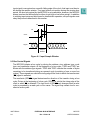
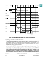
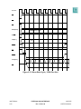
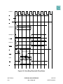
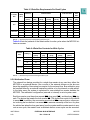
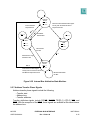
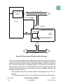
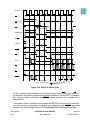
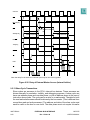
input signal is recognized on a specific falling edge of the clock, that input must be stable during the sample window. If an input makes a transition during the window time
period, the level recognized by the MPC555 is not predictable; however, the MPC555
always resolves the latched level to either a logic high or low before using it. In addition
to meeting input setup and hold times for deterministic operation, all input signals must
obey the protocols described in this section.
tho
tsu
Clock
Signal
Sample
Window
Figure 9-1 Input Sample Window
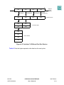
9.3 Bus Control Signals
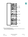
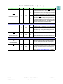
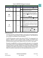
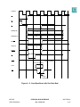
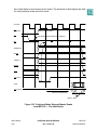
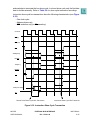
The MPC555 initiates a bus cycle by driving the address, size, address type, cycle
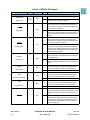
type, and read/write outputs. At the beginning of a bus cycle, TSIZ0 and TSIZ1 are
driven with the address type signals. TSIZ0 and TSIZ1 indicate the number of bytes
remaining to be transferred during an operand cycle (consisting of one or more bus
cycles). These signals are valid at the rising edge of the clock in which the transfer start
(TS) signal is asserted.
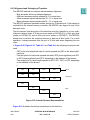
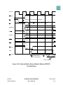
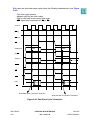
The read/write (RD/WR) signal determines the direction of the transfer during a bus
cycle. Driven at the beginning of a bus cycle, RD/WR is valid at the rising edge of the
clock in which TS is asserted. The logic level of RD/WR only changes when a write
cycle is preceded by a read cycle or vice versa. The signal may remain low for consecutive write cycles.
MOTOROLA
9-2
EXTERNAL BUS INTERFACE
Rev. 15 Nov 98
MPC555
USER’S MANUAL