1
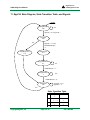
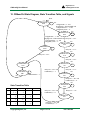
C3 Memory Module Configuration Project
User Manual
Revision: 3/20/05
TM
www .d ig ilen tinc .c om
246 East Main | Pullman, WA 99163
(509) 334 6306 Voice and Fax
1 Usage
The Digilent C3 memory module configuration project provides erasing, reading, and writing functions for the 1
MB Flash chip on the module.
2 Related Digilent Reference Projects
•
•
•
The C1MemCfg project is a similar project able to configure the Digilent C1 memory module (512 KB
RAM + 512 KB Flash) or the C0 memory module (128 KB RAM + 512 KB Flash).
The C2MemCfg project is a similar project able to configure the Digilent C2 memory module (2 x 512 KB
RAM chips, seen as a contiguous 1 MB RAM).
The C1MemCfgX2 project is an example of modifying the C1MemCfg project to support two C1 memory
modules connected to the same system board and configured through the same connection and
communication module. It can be used as model for custom projects able to support up to five Cx memory
modules (identical or different). The maximum number of memory modules is one less than the number of
available system board connectors.
When reference is made to any of these projects, the generic name CxMemCfg is used.
3 PC Required Software
•
•
Digilent TransPort and/or
MemUtil
4 The Reference Digilent Board Configuration
The ready-to-compile project is built for Spartan 3 system board with a Digilent USB 2.0 module attached to
connector A1 and a Digilent C3 memory module attached to connector A2.
5 Available Digilent Board Configurations
Compiled Bit_files and Board_Specific_Source_Files are available for:
5.1
Digilab 2FT Motherboard (Spartan XC2S300E or XC2S400E FPGA) with:
•
•
•
5.2
Digilent USB 2.0 module on A1 connector
Digilent C3 memory module on A2 connector
Digilab Digital I/O 4 on C1, C2 connectors (optional: used by Main.bit, not used by C3MemCfg.bit – see
section 6)
Digilab 2SB Motherboard with:
•
•
•
5.3
Digilent USB 2.0 module on A1 connector
Digilent C3 memory module on A2 connector
Digilab Digital I/O 4 on C1, C2 connector (optional: used by Main.bit, not used by C3MemCfg.bit – see
section 6)
Digilent Pegasus Motherboard (Spartan XC2S50 or XC2S200 FPGA) with:
•
•
Digilent USB 2.0 Module on A1 motherboard connector
Digilent C3 memory module on A2 connector
Copyright Digilent, Inc.
Page 1 of 14
Doc: 562-004
Digilent, IncTM
C3MemCfg User Manual
5.4
www.digilentinc.com
Digilent Spartan 3 Motherboard (Spartan XC3S200 or XC3S400 FPGA) with:
•
•
Digilent USB 2.0 module on A1 motherboard connector
Digilent C3 memory module on A2 connector
6 Available Project and Compiling Variants
•
•
with 7-segment display showing the lower 16 memory address bus bits (Main.bit)
without display (C3MemCfg.bit)
Choosing Main.sch as the highest level file in the project hierarchy, the project enables the display feature. The
Digilab Digital I/O 4 board should be part of the configuration or the motherboard should have the 4-digit, 7segment display on it. The compiled file is Main.bit.
Choosing C3MemCfg.sch as the highest level file in the project hierarchy disables the display feature, releasing the
associated resources (pins, internal logic). This can be done even if the whole project includes the Main.sch file, and
C3MemCtrl is displayed as a lower level hierarchical file: just highlight C3MemCtrl in the “Sources in Project” and
generate the programming file C3Memcfg.bit.
7 Digilent Library Components Used
•
•
•
C3MemCtrl
EppCtrl
Disp7sCtrl
8 Project Description
The project implements an EPP interface (EppCtrl), able to communicate with the EPP port emulated by the
Digilent USB 2.0 Module. The EPP interface controls the EPP data registers implemented in the memory module
controller (C3MemCtrl). The memory module controller generates the signal sequence needed to erase, read, or
write the Flash chip. For detailed descriptions of each component, see the Digilent Component Library.
9 Using Digilent MemUtil Software to Configure the Memory Module
Using MemUtil to configure the memory module is very simple and intuitive. You should keep in mind the features
provided by the C3 memory module (1 MB Flash). The software functions are:
•
Properties . The user sets:
o Connection Properties. In the pull-down menu, the desired connection is selected. Multiple
communication modules (Ethernet, USB, Serial) can be connected at the same time to the host PC. A
MemUtil instance uses a single such connection.
o Configure. The selected connection can be configured. For more details see the Adept User Manual.
o Memory configuration. Selects the Digilent memory module type. The C3MemCfg project works with
a single C3 memory module.
o Starting Register Address. MemUtil supports multiple memory modules attached to different
motherboard connectors. For more details, see the C1memCfgX2 project. For the C3MemCfg project,
select 0x00.
•
Load RAM. This tab is inactive, since the C3 memory module does not contain RAM memory.
•
Load Flash. The user specifies:
o the source file
o the File Start Location
o the Flash start address
o the length of transferred data block
o the Verify option
Copyright Digilent, Inc.
Page 2 of 14
Doc: 562-004
Digilent, IncTM
C3MemCfg User Manual
o
www.digilentinc.com
the Auto erase option. The software erases only the Flash block which are affected by the Load
operation.
•
Store RAM. This tab is inactive, since C3 memory module does not contain RAM memory.
•
Store Flash. The user specifies:
o the Flash start address
o the length of transferred data block
o the destination file
o the file write option (Append, Replace, Overwrite)
o the File Start Location (only for Overwrite)
•
Ease Flash. The user specifies:
o the blocks selected for erase operation
o type of operation (Erase All or Erase Selected)
Multiple instances of MemUtil can run at the same time, on the same PC, sharing the same connection,
communication module, system board, and memory module. Other Digilent applications (such as Digilent TransPort
and Digilent ExPort) can also share the same connection. The MemUtil instances sharing the same connection can
share the same memory module or be assigned to different memory modules. On the other hand, the C3MemCfg
project only supports a single C3 memory module.
Memory modules are identified by the starting register address. The C3MemCfg project assigns the starting register
address 0x00 to the memory module.
Successive operations can be launched through any active MemUtil instance. The user should allow a command to
be fully executed before launching another one for the same communication module.
To control multiple memory modules connected to the same system board (and through the same connection and
communication module), the CxMemCfg project needs to be modified. An example is the C1MemCfgX2 project.
For more information, see the C1 Memory Module Configuration X2 Project User Manual.
Multiple MemUtil instances can be used to control different board sets. For example, multiple different USB
channels can be connected each to its own set (USB Module + System Board + Memory Module). Each system
board needs to be configured with a CxMemCfg project. In this case, MemUtil instances are set to use different
connections.
10 Using Digilent TranSport Software to Configure the Memory
Module
The Transport software allows the user to access the memory module at lower level commands. The routines are the
same as the ones used by MemUtil, to implement the high level commands described above. TranSport is useful for
debugging purposes and for checking the command sequences before implementing them in a user generated
software application. The software functions are:
•
Properties . The user sets:
o Connection Properties. In the pull-down menu, the desired connection is selected. Multiple
communication modules (Ethernet, USB, Serial), can be connected at the same time to the host PC. A
MemUtil instance uses a single such connection.
o Configure. The selected connection can be configured. For more information, see the Adept User
Manual.
•
Load File. Sends a file (fragment) to a specified EPP Data Register. The user specifies:
o the source file
Copyright Digilent, Inc.
Page 3 of 14
Doc: 562-004
Digilent, IncTM
C3MemCfg User Manual
o
o
o
o
www.digilentinc.com
the File Start Location
the Destination Register
the Load Entire File option
the length of transferred data block (only if the Load Entire File option is not checked)
•
Store File. Reads a specified EPP Data Register and saves data to a file (fragment). The user specifies:
o the destination file
o the File Output Mode (Append, Replace, Overwrite)
o the File Start Location (only for Overwrite)
o the Source Register
o the length of transferred data block
•
Register I/O. Reads or writes a byte from/to a specified EPP Data Register. The user specifies:
o the Epp Register Address
o the data (for write operations)
o the read Display Format
There are 8 lines, each able to define a register address and data. Their transfer can be performed line by line
(pressing the Read or Write button of the desired line) or as full sequence, pressing the Read All or Write All
buttons.
Multiple instances of TransPort can run at the same time, on the same PC, sharing the same connection,
communication module, system board, and memory module. Other Digilent applications (such as MemUtil and
ExPort) can also share the same connection. The TransPort instances sharing the same connection can share the
same memory module or be assigned to different memory modules. On the other hand, the C2MemCfg project only
supports a single C3 memory module.
Memory modules are identified by the Register Address range. The C3MemCfg project assigns the Register Address
range 0x00 ...0x07 to the memory module.
Successive operations can be launched through any active TransPort instance. The user should however allow a
command to be fully executed before launching another one for the same communication module.
To control multiple memory modules connected to the same system board (and through the same connection and
communication module), the CxMemCfg project needs to be modified. An example is the C1MemCfgX2 project.
For more details see the C1Memory Configuration X2 Project User Manual.
Multiple TransPort instances can be used to control different board sets. For example, multiple different USB
channels can be connected each to its own set (USB Module + System Board + Memory Module). Each system
board needs to be configured with a CxMemCfg project. In this case, TransPort instances are set to use different
connections.
As described above, TransPort software can be used to control any EPP interface implemented in the FPGA circuit.
The following section shows how to access the specific C3 memory module features.
10.1 Reading a Flash Location with Low-Level EPP Commands
Before attempting to read the Flash memory, make sure the Flash is in the Array Read mode. The Flash chip can be
set in Array Read mode by either of the following actions:
•
•
•
Power up reset
Activate the Reset pin (RP) (active LOW)
Issue the READ ARRAY command.
Once in READ ARRAY mode, the Flash chip holds that mode until a different command is sent.
Copyright Digilent, Inc.
Page 4 of 14
Doc: 562-004
Digilent, IncTM
C3MemCfg User Manual
www.digilentinc.com
If the Flash chip is already in READ ARRAY mode, skip the steps 1 to 2.
1. Load Read Array command to the Memory Data Bus Register MemDB(7 downto 0)):
1.1. Write the Read Array command (FFh) to EPP Register regMemWrData(7 downto 0) at EPP address
MemDataWr = 4
2. Generate the write sequence on the memory control bus:
2.1. Activate FlashCS and MemWr signals - write “10101” to the regMemCtl(4 downto 0), at EPP address
MemCtrlReg = 0)
2.2. Deactivate MemWr signal - write “10111” to the regMemCtl(4 downto 0), at EPP address MemCtrlReg =
0)
2.3. Deactivate FlashCS signal - write “11111” to the regMemCtl(4 downto 0), at EPP address MemCtrlReg =
0)
3. Load the Memory Address Bus Register (MemAdr(19 downto 0)):
3.1. Write the lowest address byte to EPP Register MemAdr(7 downto 0) at EPP address MemAdrL = 1
3.2. Write the middle address byte to EPP Register MemAdr(15 downto 8) at EPP address MemAdrM = 2
3.3. Write the highest address byte to EPP Register MemAdr(19 downto 16) at EPP address MemAdrH = 3
(for bytes keeping the previous value, the steps above can be skipped)
4. Generate the read sequence on the memory control bus:
4.1. Activate FlashCS and MemOE signals - write “10110” to the regMemCtl(4 downto 0), at EPP address
MemCtrlReg = 0)
5. Read the Memory Data Bus Register MemDB(7 downto 0)):
5.1. Read the EPP Register regMemRdData(7 downto 0) at EPP address MemDataRd = 5
6. Finish the read sequence on the memory control bus:
6.1. Deactivate FlashCS and MemOE signals - write “11111” to the regMemCtl(4 downto 0), at EPP address
MemCtrlReg = 0)
10.2 Writing a Flash Location with Low-Level EPP Commands
The user directly controls the memory busses (Data, Address and Control), using the Register I/O function:
1. Load the Memory Address Bus Register (MemAdr(19 downto 0)):
1.1. Write the lowest address byte to EPP Register MemAdr(7 downto 0) at EPP address MemAdrL = 1
1.2. Write the middle address byte to EPP Register MemAdr(15 downto 8) at EPP address MemAdrM = 2
1.3. Write the highest address byte to EPP Register MemAdr(19 downto 16) at EPP address MemAdrH = 3
(for bytes keeping the previous value, the steps above can be skipped)
2. Load Write Command to the Memory Data Bus Register MemDB(7 downto 0)):
2.1. Write the Write Command (40h) to EPP Register regMemWrData(7 downto 0) at EPP address
MemDataWr = 4
3. Generate the write sequence on the memory control bus:
3.1. Activate FlashCS and MemWr signals - write “10101” to the regMemCtl(4 downto 0), at EPP address
MemCtrlReg = 0)
3.2. Deactivate MemWr signal - write “10111” to the regMemCtl(4 downto 0), at EPP address MemCtrlReg =
0)
3.3. Deactivate FlashCS signal - write “11111” to the regMemCtl(4 downto 0), at EPP address MemCtrlReg =
0)
4. Load data to the Memory Data Bus Register MemDB(7 downto 0)):
4.1. Write the data byte to EPP Register regMemWrData(7 downto 0) at EPP address MemDataWr = 4
5. Generate the write sequence on the memory control bus:
5.1. Activate FlashCS and MemWr signals - write “10101” to the regMemCtl(4 downto 0), at EPP address
MemCtrlReg = 0)
5.2. Deactivate MemWr signal - write “10111” to the regMemCtl(4 downto 0), at EPP address MemCtrlReg =
0)
5.3. Deactivate FlashCS signal - write “11111” to the regMemCtl(4 downto 0), at EPP address MemCtrlReg =
0)
Copyright Digilent, Inc.
Page 5 of 14
Doc: 562-004
Digilent, IncTM
C3MemCfg User Manual
www.digilentinc.com
When manually writing a data byte using TransPort software, the steps 6 to 13 are not necessary (in fact, it’s not
possible to perform them fast enough.) They check a status bit of the Flash chip, which pulses low, while the internal
Flash logic performs the write operation. Typical pulse length is 2µs. The steps are posted here as a reference to be
implemented in a software or HDL component, which automatically performs the write sequence.
6.
7.
8.
9.
10.
11.
12.
13.
Generate the read sequence on the memory control bus:
6.1. Activate FlashCS and MemOE signals - write “10110” to the regMemCtl(4 downto 0), at EPP address
MemCtrlReg = 0)
Read the Flash Status Register (SR) on the Memory Data Bus Register MemDB(7 downto 0)):
7.1. Read the EPP Register regMemRdData(7 downto 0) at EPP address MemDataRd = 5
Finish the read sequence on the memory control bus:
8.1. Deactivate FlashCS and MemOE signals - write “11111” to the regMemCtl(4 downto 0), at EPP address
MemCtrlReg = 0)
Check the SR7 bit (MSB of SR). Loop back to 6, if SR7 = 1.
Generate the read sequence on the memory control bus:
10.1. Activate FlashCS and MemOE signals - write “10110” to the regMemCtl(4 downto 0), at EPP address
MemCtrlReg = 0)
Read the Flash Status Register (SR) on the Memory Data Bus Register MemDB(7 downto 0)):
11.1. Read the EPP Register regMemRdData(7 downto 0) at EPP address MemDataRd = 5
Finish the read sequence on the memory control bus:
12.1. Deactivate FlashCS and MemOE signals - write “11111” to the regMemCtl(4 downto 0), at EPP address
MemCtrlReg = 0)
Check the SR7 bit (MSB of SR). Loop back to 10 , if SR7 = 0.
10.3 Erasing a Flash Block with Low-Level EPP Commands
The user directly controls the memory busses (Data, Address and Control), using the Register I/O function:
1. Load the Memory Address Bus Register (MemAdr(19 downto 0)) – any address in the block to be erased:
1.1. Write the lowest address byte to EPP Register MemAdr(7 downto 0) at EPP address MemAdrL = 1
1.2. Write the middle address byte to EPP Register MemAdr(15 downto 8) at EPP address MemAdrM = 2
1.3. Write the highest address byte to EPP Register MemAdr(19 downto 16) at EPP address MemAdrH = 3
(for bytes keeping the previous value, the steps above can be skipped)
2. Load Erase Command to the Memory Data Bus Register MemDB(7 downto 0)):
2.1. Write the Erase Command (20h) to EPP Register regMemWrData(7 downto 0) at EPP address
MemDataWr = 4
3. Generate the write sequence on the memory control bus:
3.1. Activate FlashCS and MemWr signals - write “10101” to the regMemCtl(4 downto 0), at EPP address
MemCtrlReg = 0)
3.2. Deactivate MemWr signal - write “10111” to the regMemCtl(4 downto 0), at EPP address MemCtrlReg =
0)
3.3. Deactivate FlashCS signal - write “11111” to the regMemCtl(4 downto 0), at EPP address MemCtrlReg =
0)
4. Load Confirm Erase Command to the Memory Data Bus Register MemDB(7 downto 0)):
4.1. Write the Confirm Erase Command (D0h) to EPP Register regMemWrData(7 downto 0) at EPP address
MemDataWr = 4
5. Generate the write sequence on the memory control bus:
5.1. Activate FlashCS and MemWr signals - write “10101” to the regMemCtl(4 downto 0), at EPP address
MemCtrlReg = 0)
5.2. Deactivate MemWr signal - write “10111” to the regMemCtl(4 downto 0), at EPP address MemCtrlReg =
0)
5.3. Deactivate FlashCS signal - write “11111” to the regMemCtl(4 downto 0), at EPP address MemCtrlReg =
0)
When manually writing a data byte using TransPort software, the steps 6 to 13 are not necessary (in fact, it’s not
possible to perform them fast enough.) They check a status bit of the Flash chip, which pulses low, while the internal
Copyright Digilent, Inc.
Page 6 of 14
Doc: 562-004
Digilent, IncTM
C3MemCfg User Manual
www.digilentinc.com
Flash logic performs the write operation. Typical pulse length is 200-500ms. The steps are posted here as a reference
to be implemented in a software or HDL component, which performs automatically the erase sequence.
6.
7.
8.
9.
10.
11.
12.
13.
Generate the read sequence on the memory control bus:
6.1. Activate FlashCS and MemOE signals - write “10110” to the regMemCtl(4 downto 0), at EPP address
MemCtrlReg = 0)
Read the Flash Status Register (SR) on the Memory Data Bus Register MemDB(7 downto 0)):
7.1. Read the EPP Register regMemRdData(7 downto 0) at EPP address MemDataRd = 5
Finish the read sequence on the memory control bus:
8.1. Deactivate FlashCS and MemOE signals - write “11111” to the regMemCtl(4 downto 0), at EPP address
MemCtrlReg = 0)
Check the SR7 bit (MSB of SR). Loop back to 6, if SR7 = 1.
Generate the read sequence on the memory control bus:
10.1. Activate FlashCS and MemOE signals - write “10110” to the regMemCtl(4 downto 0), at EPP address
MemCtrlReg = 0)
Read the Flash Status Register (SR) on the Memory Data Bus Register MemDB(7 downto 0)):
11.1. Read the EPP Register regMemRdData(7 downto 0) at EPP address MemDataRd = 5
Finish the read sequence on the memory control bus:
12.1. Deactivate FlashCS and MemOE signals - write “11111” to the regMemCtl(4 downto 0), at EPP address
MemCtrlReg = 0)
Check the SR7 bit (MSB of SR). Loop back to 10 , if SR7 = 0.
10.4 Reading a Flash Location Using the Automatic Flash Read Register
Before attempting to read the Flash memory, make sure the Flash is in the Array Read mode. The Flash chip can be
set in Array Read mode by either of the following actions:
•
•
•
Power up reset
Activate the Reset pin (RP) (active LOW)
Issue the READ ARRAY command.
Once in READ ARRAY mode, the Flash chip holds that mode until a different command is sent.
If the Flash chip is not already in READ ARRAY mode, perform first the steps 1 to 2 shown in section 10.1.
1.
2.
Load the Memory Address Bus Register (MemAdr(19 downto 0)):
1.1. Write the lowest address byte to EPP Register MemAdr(7 downto 0) at EPP address MemAdrL = 1
1.2. Write the middle address byte to EPP Register MemAdr(15 downto 8) at EPP address MemAdrM = 2
1.3. Write the highest address byte to EPP Register MemAdr(19 downto 16) at EPP address MemAdrH = 3
(for bytes keeping the previous value, the steps above can be skipped)
Read the regMemRdData(7 downto 0) register at address RamAutoRW = 7. C3MemCtrl automatically
generates the read sequence and increments the MemAdr register. Repeat step 2 to read successive Flash
locations.
10.5 Writing a Flash Location Using the Automatic Flash Write Register
1.
2.
Load the Memory Address Bus Register (MemAdr(19 downto 0)):
1.1. Write the lowest address byte to EPP Register MemAdr(7 downto 0) at EPP address MemAdrL = 1
1.2. Write the middle address byte to EPP Register MemAdr(15 downto 8) at EPP address MemAdrM = 2
1.3. Write the highest address byte to EPP Register MemAdr(19 downto 16) at EPP address MemAdrH = 3
(for bytes keeping the previous value, the steps above can be skipped)
Write data byte to the regMemRdData(7 downto 0) register at address FlashAutoRW = 7. C3MemCtrl
automatically generates the write sequence and increments the MemAdr register. Repeat step 2 to write
successive Flash locations. The Flash chip enters the READ STATUS mode.
Copyright Digilent, Inc.
Page 7 of 14
Doc: 562-004
Digilent, IncTM
C3MemCfg User Manual
www.digilentinc.com
10.6 Storing the Flash Content to a File Using the Store File Function
Before attempting to read the Flash memory, make sure the Flash is in the Array Read mode. The Flash chip can be
set in Array Read mode by either of the following actions:
•
•
•
Power up reset
Activate the Reset pin (RP) (active LOW)
Issue the READ ARRAY command.
Once in READ ARRAY mode, the Flash chip holds that mode until a different command is sent.
If the Flash chip is not already in READ ARRAY mode, perform first the steps 1 to 2 shown in section 10.1.
1.
2.
Load the Memory Address Bus Register (MemAdr(19 downto 0)):
1.1. Write the lowest address byte to EPP Register MemAdr(7 downto 0) at EPP address MemAdrL = 1
1.2. Write the middle address byte to EPP Register MemAdr(15 downto 8) at EPP address MemAdrM = 2
1.3. Write the highest address byte to EPP Register MemAdr(19 downto 16) at EPP address MemAdrH = 3
(for bytes keeping the previous value, the steps above can be skipped)
Select the Store File tab of the TransPort software. Fill in the required fields. Select Source Register 7
(FlashAutoRW). Press the Store button.
10.7 Loading a File to the Flash Using the Load File Function
1.
2.
Load the Memory Address Bus Register (MemAdr(19 downto 0)):
1.1. Write the lowest address byte to EPP Register MemAdr(7 downto 0) at EPP address MemAdrL = 1
1.2. Write the middle address byte to EPP Register MemAdr(15 downto 8) at EPP address MemAdrM = 2
1.3. Write the highest address byte to EPP Register MemAdr(19 downto 16) at EPP address MemAdrH = 3
(for bytes keeping the previous value, the steps above can be skipped)
Select the Load File tab of the TransPort software. Fill in the required fields. Select Source Register 7
(FlashAutoRW). Press the Load button. The Flash chip enters the READ STATUS mode.
Copyright Digilent, Inc.
Page 8 of 14
Doc: 562-004
Digilent, IncTM
C3MemCfg User Manual
www.digilentinc.com
11 EppCtrl State Diagram, State Transition Table, and Signals
EppRst
stEppReady
000
else
eppDstb = '0' or eppAstb =
stEppStb
010
else
EppDstb = ‘0’ and
HandShakeReqIn =
‘1’
stEppSetProc
011
stEppRegTransf
110
stEppLaunchProc
111
else
ctlMsmDoneIn = '1'
stEppWaitPro
c
else
ctlMsmDoneIn = '0'
stEppDone
100
EppAstb = '0' or
EppDstb = ‘0’
else
State Transition Table
00
01
11
10
Copyright Digilent, Inc.
Page 9 of 14
0
Ready
↓
Stb
↓ →
RegTransf
↓
Done
1
SetProc
↓
LaunchProc
↓
WaitProc
Doc: 562-004
Digilent, IncTM
C3MemCfg User Manual
www.digilentinc.com
11.1 EppCtrl Port Signals
-- EPP-like bus signals
clk
: in std_logic;
-- system clock (50MHz)
EppAstb
: in std_logic;
-- Address strobe
EppDstb
: in std_logic;
-- Data strobe
EppWr
: in std_logic;
-- Port write signal
EppRst
: in std_logic;
-- Port reset signal
EppDB
: inout std_logic_vector(7 downto 0); -- port data bus
EppWait : out std_logic;
-- Port wait signal
-- User signals
busEppOut
: out std_logic_vector(7 downto 0);-- Data Output bus
busEppIn
: in std_logic_vector(7 downto 0); -- Data Input bus
ctlEppDwrOut : out std_logic; -- Data Write pulse
ctlEppRdCycleOut: inout std_logic;-- Indicates a READ Epp cycle
regEppAdrOut : inout std_logic_vector(7 downto 0) := "00000000"; -- Epp Address Register content
HandShakeReqIn : in std_logic;
-- User Handshake Request
ctlEppStartOut : out std_logic; -- Automatic process Start
ctlEppDoneIn
: in std_logic
-- Automatic process Done
11.2 EppCtrl Internal Signals
busEppInternal: std_logic_vector(7 downto 0);
ctlEppAwr
: std_logic;
11.3 EppCtrl Signal Assignments
-- Synchronized EPP outputs:
process(clk)
begin
if clk'event and clk='1' then
if stEppCur = stEppReady then
ctlEppRdCycleOut <= '0';
elsif stEppCur = stEppStb then
ctlEppRdCycleOut <= EppWr;
state
end if;
end if;
end process;
-- not equivalent to EppWr due to default
busEppOut <= EppDB;
EppDB <=
busEppInternal when (ctlEppRdCycleOut = '1') else "ZZZZZZZZ";
busEppInternal <= regEppAdrOut when EppAstb = '0' else busEppIn;
-- Epp State machine related signals
EppWait <= '1' when stEppCur = stEppDone else '0';
ctlEppAwr <= '1' when stEppCur = stEppRegTransf and EppAstb = '0' and EppWr = '0' else '0';
ctlEppDwrOut <= '1' when (stEppCur = stEppRegTransf or stEppCur = stEppSetProc)
and EppDstb = '0' and EppWr = '0' else '0';
ctlEppStartOut <= '1' when stEppCur = stEpplaunchProc else '0';
Copyright Digilent, Inc.
Page 10 of 14
Doc: 562-004
Digilent, IncTM
C3MemCfg User Manual
www.digilentinc.com
12 C3MemCtrl State Diagram, State Transition Table, and Signals
Reset
stMsmReady
0000
else
CtlEppStartIn = ‘1’ and
RegEppAdr = FlashAutoRW and
ComponentSelect = ‘1’ and
CtlEppRdCycleIn = ‘0’
else
stMsmFwr01
0001
CtlEppStartIn = ‘1’ and
RegEppAdr = FlashAutoRW and DelayCnt = “101”
ComponentSelect = ‘1’ and
else
CtlEppRdCycleIn = ‘1’
stMsmFwr02
0101
stMsmFrd01
0100
DelayCnt = “111”
else
else
stMsmFwr03
DelayCnt = “101”
0111
DelayCnt = “101”
stMsmAdInc
1100
stMsmDone
1000
else
stMsmFwr04
1111
DelayCnt = “101” and
busMemIn(7) = ‘1’
CtlMsmStartIn = ‘’1’
01
11
10
00
Ready
↓ →
Frd01
↓
AdrInc
↓
Done
↓
01
Fwr01
11
10
↓
Fwr02
DelayCnt = “101” and
busMemIn(7) = ‘0’
Fwr03
→
Fwr07
↓
←
DelayCnt = “111”
else
stMsmFwr07
1101
Fwr04
Fwr06
DelayCnt = “111”
else
stMsmFwr05
1011
DelayCnt = “101” and
busMemIn(7) = ‘0’
else
stMsmFwr06
1001
State Transition Table
00
else
↓
Fwr05
↑
Copyright Digilent, Inc.
←
DelayCnt = “101” and
busMemIn(7) = ‘1’
Page 11 of 14
Doc: 562-004
Digilent, IncTM
C3MemCfg User Manual
www.digilentinc.com
12.1 C3MemCtrl Port Signals
ck
: in std_logic;
-- system clock (50MHz)
-- EPP interface signals
HandShakeReqOut:
out std_logic;
-- User Handshake Request
ctlMsmStartIn:
in std_logic;
-- Automatic process Start
ctlMsmDoneOut:
out std_logic;
-- Automatic process Done
ctlMsmDwrIn:
in std_logic;
-- Data Write pulse
ctlEppRdCycleIn:
in std_logic;
-- Indicates a READ Epp cycle
EppRdDataOut:
out std_logic_vector(7 downto 0); -- Data Input bus
EppWrDataIn:
in std_logic_vector(7 downto 0); -- Data Output bus
regEppAdrIn:
in std_logic_vector(7 downto 0) ; -- Epp Address Register content (bits 7:3 ignored)
ComponentSelect : in std_logic;
-- active HIGH, selects the current MemCtrl instance
-- Memory bus signals
MemDB
: inout std_logic_vector(7 downto 0); -- Memory data bus
MemAdr
: out std_logic_vector(19 downto 0); -- Memory Address bus
FlashCS
: out std_logic; -- Flash CS
MemWR
: out std_logic; -- memory write
MemOE
: out std_logic -- memory read (Output Enable), also controls the MemDB direction
12.2 C3MemCtrl Internal Signals
signal
DelayCnt
: std_logic_vector(2 downto 0);
-- Signals dealing with memory chips
signal regMemCtl:
std_logic_vector(4 downto 0) := "11111";-- Memory Control register
signal regMemAdr:
std_logic_vector(19 downto 0);
-- Memory Address register
signal carryoutL:
std_logic := '0';
-- Carry out for memory address low byte
signal carryoutM:
std_logic := '0';
-- Carry out for memory address middle byte
signal regMemWrData: std_logic_vector(7 downto 0);
-- Memory Write Data register
signal regMemRdData: std_logic_vector(7 downto 0);
-- Memory Read Data register
signal busMemIn:
std_logic_vector(7 downto 0);
signal busMemOut:
std_logic_vector(7 downto 0);
-- Signals in the memory control register
signal ctlMcrOe
: std_logic;
signal ctlMcrWr
: std_logic;
signal ctlMcrFlashCs : std_logic;
signal ctlMcrDir
: std_logic;
-- Output enable (read strobe)
-- Write enable (write strobe)
-- Flash chip select
-- composed out of previous ones
-- Signals used by Memory control state machine
signal ctlMsmOe
: std_logic;
signal ctlMsmWr
: std_logic;
signal ctlMsmFlashCs : std_logic;
signal ctlMsmDir
: std_logic;
signal ctlMsmAdrInc : std_logic;
signal ctlMsmWrCmd : std_logic;
Copyright Digilent, Inc.
Page 12 of 14
Doc: 562-004
Digilent, IncTM
C3MemCfg User Manual
www.digilentinc.com
12.3 C3MemCtrl Signal Assignments
-- Memory signals
-Memory control register
ctlMcrOe
<= regMemCtl(0);
ctlMcrWr
<= regMemCtl(1);
ctlMcrFlashCs <= regMemCtl(3);
-- Output enable (read strobe)
-- Write enable (write strobe)
-- Flash chip select
-- Memory control bus driven either by automatic state machine or by memory control register
FlashCS
<= ctlMsmFlashCs and ctlMcrFlashCs;
-- PC generated Flash CS;
MemWR
<= ctlMsmWr and ctlMcrWr;
-- PC generated MemWr;
MemOE
<= ctlMsmOe and ctlMcrOe;
-- PC generated MemOe;
busMemIn
<= MemDB;
busMemOut
<= "01000000" when ctlMsmWrCmd = '1' else regMemWrData;
MemAdr
<= regMemAdr;
ctlMcrDir
<= ctlMcrOe and ((not ctlMcrFlashCs) or (not ctlMcrRAMCs));
MemDB
<= busMemOut when (ctlMsmDir = '1' or ctlMcrDir = '1') else "ZZZZZZZZ";
-- Handshake signal
HandShakeReqOut <=
'1'
when (regEppAdrIn(2 downto 0) = FlashAutoRW)
and ComponentSelect = '1' else
'0';
-- Delay Counter
process (clk)
begin
if clk'event and clk = '1' then
if stMsmCur = stMsmReady then DelayCnt <= "000";
else DelayCnt <= DelayCnt + 1;
end if;
end if;
end process;
-- Memory Control Register
process (clk, ctlMsmDwrIn)
begin
if clk = '1' and clk'Event then
if ctlMsmDwrIn = '1' and regEppAdrIn(2 downto 0) = MemCtrlReg and ComponentSelect = '1' then
regMemCtl <= EppWrDataIn(4 downto 0);
end if;
end if;
end process;
-- Memory Address Register/Counter
MsmAdrL:
process (clk, ctlMsmDwrIn, ctlMsmAdrInc)
begin
if clk = '1' and clk'Event then
if ctlMsmAdrInc = '1' then
regMemAdr(7 downto 0) <= regMemAdr(7 downto 0) + 1; --"00000001";
elsif ctlMsmDwrIn = '1' and regEppAdrIn(2 downto 0) = MemAdrL and ComponentSelect = '1' then
regMemAdr(7 downto 0) <= EppWrDataIn;
end if;
end if;
Copyright Digilent, Inc.
Page 13 of 14
Doc: 562-004
Digilent, IncTM
C3MemCfg User Manual
www.digilentinc.com
end process;
carryoutL <= '1' when regMemAdr(7 downto 0) = "11111111" else '0';
MsmAdrM:
process (clk, ctlMsmDwrIn, ctlMsmAdrInc)
begin
if clk = '1' and clk'Event then
if ctlMsmAdrInc = '1' and carryoutL = '1' then
regMemAdr(15 downto 8) <= regMemAdr(15 downto 8) + 1; --"00000001";
elsif ctlMsmDwrIn = '1' and regEppAdrIn(2 downto 0) = MemAdrM and ComponentSelect = '1' then
regMemAdr(15 downto 8) <= EppWrDataIn;
end if;
end if;
end process;
carryoutM <= '1' when regMemAdr(15 downto 8) = "11111111" else '0';
MsmAdrH:
process (clk, ctlMsmDwrIn, ctlMsmAdrInc)
begin
if clk = '1' and clk'Event then
if ctlMsmAdrInc = '1' and carryoutL = '1' and carryoutM = '1' then
regMemAdr(19 downto 16) <= regMemAdr(19 downto 16) + 1; --"001";
elsif ctlMsmDwrIn = '1' and regEppAdrIn(2 downto 0) = MemAdrH and ComponentSelect = '1' then
regMemAdr(19 downto 16) <= EppWrDataIn(2 downto 0);
end if;
end if;
end process;
-- Memory write data holding register
process (clk, ctlMsmDwrIn)
begin
if clk = '1' and clk'Event then
if ctlMsmDwrIn = '1' and
(regEppAdrIn(2 downto 0) = FlashAutoRW or
regEppAdrIn(2 downto 0) = MemDataWr) and ComponentSelect = '1' then
regMemWrData <= EppWrDataIn;
end if;
end if;
end process;
-- Memory read register: - holds data after an automatic read
process (clk)
begin
if clk = '1' and clk'Event then
if
stMsmCur = stMsmFrd01 then
regMemRdData <= busMemIn;
end if;
end if;
end process;
Copyright Digilent, Inc.
Page 14 of 14
Doc: 562-004