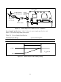
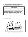
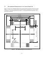
1
To our customers,
Old Company Name in Catalogs and Other Documents
On April 1st, 2010, NEC Electronics Corporation merged with Renesas Technology
Corporation, and Renesas Electronics Corporation took over all the business of both
companies. Therefore, although the old company name remains in this document, it is a valid
Renesas Electronics document. We appreciate your understanding.
Renesas Electronics website: http://www.renesas.com
April 1st, 2010
Renesas Electronics Corporation
Issued by: Renesas Electronics Corporation (http://www.renesas.com)
Send any inquiries to http://www.renesas.com/inquiry.
Notice
1.
2.
3.
4.
5.
6.
7.
All information included in this document is current as of the date this document is issued. Such information, however, is
subject to change without any prior notice. Before purchasing or using any Renesas Electronics products listed herein, please
confirm the latest product information with a Renesas Electronics sales office. Also, please pay regular and careful attention to
additional and different information to be disclosed by Renesas Electronics such as that disclosed through our website.
Renesas Electronics does not assume any liability for infringement of patents, copyrights, or other intellectual property rights
of third parties by or arising from the use of Renesas Electronics products or technical information described in this document.
No license, express, implied or otherwise, is granted hereby under any patents, copyrights or other intellectual property rights
of Renesas Electronics or others.
You should not alter, modify, copy, or otherwise misappropriate any Renesas Electronics product, whether in whole or in part.
Descriptions of circuits, software and other related information in this document are provided only to illustrate the operation of
semiconductor products and application examples. You are fully responsible for the incorporation of these circuits, software,
and information in the design of your equipment. Renesas Electronics assumes no responsibility for any losses incurred by
you or third parties arising from the use of these circuits, software, or information.
When exporting the products or technology described in this document, you should comply with the applicable export control
laws and regulations and follow the procedures required by such laws and regulations. You should not use Renesas
Electronics products or the technology described in this document for any purpose relating to military applications or use by
the military, including but not limited to the development of weapons of mass destruction. Renesas Electronics products and
technology may not be used for or incorporated into any products or systems whose manufacture, use, or sale is prohibited
under any applicable domestic or foreign laws or regulations.
Renesas Electronics has used reasonable care in preparing the information included in this document, but Renesas Electronics
does not warrant that such information is error free. Renesas Electronics assumes no liability whatsoever for any damages
incurred by you resulting from errors in or omissions from the information included herein.
Renesas Electronics products are classified according to the following three quality grades: “Standard”, “High Quality”, and
“Specific”. The recommended applications for each Renesas Electronics product depends on the product’s quality grade, as
indicated below. You must check the quality grade of each Renesas Electronics product before using it in a particular
application. You may not use any Renesas Electronics product for any application categorized as “Specific” without the prior
written consent of Renesas Electronics. Further, you may not use any Renesas Electronics product for any application for
which it is not intended without the prior written consent of Renesas Electronics. Renesas Electronics shall not be in any way
liable for any damages or losses incurred by you or third parties arising from the use of any Renesas Electronics product for an
application categorized as “Specific” or for which the product is not intended where you have failed to obtain the prior written
consent of Renesas Electronics. The quality grade of each Renesas Electronics product is “Standard” unless otherwise
expressly specified in a Renesas Electronics data sheets or data books, etc.
“Standard”:
8.
9.
10.
11.
12.
Computers; office equipment; communications equipment; test and measurement equipment; audio and visual
equipment; home electronic appliances; machine tools; personal electronic equipment; and industrial robots.
“High Quality”: Transportation equipment (automobiles, trains, ships, etc.); traffic control systems; anti-disaster systems; anticrime systems; safety equipment; and medical equipment not specifically designed for life support.
“Specific”:
Aircraft; aerospace equipment; submersible repeaters; nuclear reactor control systems; medical equipment or
systems for life support (e.g. artificial life support devices or systems), surgical implantations, or healthcare
intervention (e.g. excision, etc.), and any other applications or purposes that pose a direct threat to human life.
You should use the Renesas Electronics products described in this document within the range specified by Renesas Electronics,
especially with respect to the maximum rating, operating supply voltage range, movement power voltage range, heat radiation
characteristics, installation and other product characteristics. Renesas Electronics shall have no liability for malfunctions or
damages arising out of the use of Renesas Electronics products beyond such specified ranges.
Although Renesas Electronics endeavors to improve the quality and reliability of its products, semiconductor products have
specific characteristics such as the occurrence of failure at a certain rate and malfunctions under certain use conditions. Further,
Renesas Electronics products are not subject to radiation resistance design. Please be sure to implement safety measures to
guard them against the possibility of physical injury, and injury or damage caused by fire in the event of the failure of a
Renesas Electronics product, such as safety design for hardware and software including but not limited to redundancy, fire
control and malfunction prevention, appropriate treatment for aging degradation or any other appropriate measures. Because
the evaluation of microcomputer software alone is very difficult, please evaluate the safety of the final products or system
manufactured by you.
Please contact a Renesas Electronics sales office for details as to environmental matters such as the environmental
compatibility of each Renesas Electronics product. Please use Renesas Electronics products in compliance with all applicable
laws and regulations that regulate the inclusion or use of controlled substances, including without limitation, the EU RoHS
Directive. Renesas Electronics assumes no liability for damages or losses occurring as a result of your noncompliance with
applicable laws and regulations.
This document may not be reproduced or duplicated, in any form, in whole or in part, without prior written consent of Renesas
Electronics.
Please contact a Renesas Electronics sales office if you have any questions regarding the information contained in this
document or Renesas Electronics products, or if you have any other inquiries.
(Note 1) “Renesas Electronics” as used in this document means Renesas Electronics Corporation and also includes its majorityowned subsidiaries.
(Note 2) “Renesas Electronics product(s)” means any product developed or manufactured by or for Renesas Electronics.
To all our customers
Regarding the change of names mentioned in the document, such as Hitachi
Electric and Hitachi XX, to Renesas Technology Corp.
The semiconductor operations of Mitsubishi Electric and Hitachi were transferred to Renesas
Technology Corporation on April 1st 2003. These operations include microcomputer, logic, analog
and discrete devices, and memory chips other than DRAMs (flash memory, SRAMs etc.)
Accordingly, although Hitachi, Hitachi, Ltd., Hitachi Semiconductors, and other Hitachi brand
names are mentioned in the document, these names have in fact all been changed to Renesas
Technology Corp. Thank you for your understanding. Except for our corporate trademark, logo and
corporate statement, no changes whatsoever have been made to the contents of the document, and
these changes do not constitute any alteration to the contents of the document itself.
Renesas Technology Home Page: http://www.renesas.com
Renesas Technology Corp.
Customer Support Dept.
April 1, 2003
Cautions
Keep safety first in your circuit designs!
1.
Renesas Technology Corporation puts the maximum effort into making semiconductor products better and more reliable, but
there is always the possibility that trouble may occur with them. Trouble with semiconductors may lead to personal injury, fire
or property damage.
Remember to give due consideration to safety when making your circuit designs, with appropriate measures such as (i)
placement of substitutive, auxiliary circuits, (ii) use of nonflammable material or (iii) prevention against any malfunction or
mishap.
Notes regarding these materials
1.
These materials are intended as a reference to assist our customers in the selection of the Renesas Technology Corporation
product best suited to the customer's application; they do not convey any license under any intellectual property rights, or any
other rights, belonging to Renesas Technology Corporation or a third party.
2.
Renesas Technology Corporation assumes no responsibility for any damage, or infringement of any third-party's rights,
originating in the use of any product data, diagrams, charts, programs, algorithms, or circuit application examples contained in
these materials.
3.
All information contained in these materials, including product data, diagrams, charts, programs and algorithms represents
information on products at the time of publication of these materials, and are subject to change by Renesas Technology
Corporation without notice due to product improvements or other reasons. It is therefore recommended that customers contact
Renesas Technology Corporation or an authorized Renesas Technology Corporation product distributor for the latest product
information before purchasing a product listed herein.
The information described here may contain technical inaccuracies or typographical errors.
Renesas Technology Corporation assumes no responsibility for any damage, liability, or other loss rising from these
inaccuracies or errors.
Please also pay attention to information published by Renesas Technology Corporation by various means, including the
Renesas Technology Corporation Semiconductor home page (http://www.renesas.com).
4.
When using any or all of the information contained in these materials, including product data, diagrams, charts, programs, and
algorithms, please be sure to evaluate all information as a total system before making a final decision on the applicability of
the information and products. Renesas Technology Corporation assumes no responsibility for any damage, liability or other
loss resulting from the information contained herein.
5.
Renesas Technology Corporation semiconductors are not designed or manufactured for use in a device or system that is used
under circumstances in which human life is potentially at stake. Please contact Renesas Technology Corporation or an
authorized Renesas Technology Corporation product distributor when considering the use of a product contained herein for
any specific purposes, such as apparatus or systems for transportation, vehicular, medical, aerospace, nuclear, or undersea
repeater use.
6.
The prior written approval of Renesas Technology Corporation is necessary to reprint or reproduce in whole or in part these
materials.
7.
If these products or technologies are subject to the Japanese export control restrictions, they must be exported under a license
from the Japanese government and cannot be imported into a country other than the approved destination.
Any diversion or reexport contrary to the export control laws and regulations of Japan and/or the country of destination is
prohibited.
8.
Please contact Renesas Technology Corporation for further details on these materials or the products contained therein.
User’s Manual
SH7729 E10A
Emulation Memory Board
(HS7729EJH01H, HS7709AEJH01H)
User’s Manual
Rev.1.0 2002.09
Cautions
1. Hitachi neither warrants nor grants licenses of any rights of Hitachi’s or any third party’s
patent, copyright, trademark, or other intellectual property rights for information contained in
this document. Hitachi bears no responsibility for problems that may arise with third party’s
rights, including intellectual property rights, in connection with use of the information
contained in this document.
2. Products and product specifications may be subject to change without notice. Confirm that you
have received the latest product standards or specifications before final design, purchase or
use.
3. Hitachi makes every attempt to ensure that its products are of high quality and reliability.
However, contact Hitachi’s sales office before using the product in an application that
demands especially high quality and reliability or where its failure or malfunction may directly
threaten human life or cause risk of bodily injury, such as aerospace, aeronautics, nuclear
power, combustion control, transportation, traffic, safety equipment or medical equipment for
life support.
4. Design your application so that the product is used within the ranges guaranteed by Hitachi
particularly for maximum rating, operating supply voltage range, heat radiation characteristics,
installation conditions and other characteristics. Hitachi bears no responsibility for failure or
damage when used beyond the guaranteed ranges. Even within the guaranteed ranges,
consider normally foreseeable failure rates or failure modes in semiconductor devices and
employ systemic measures such as fail-safes, so that the equipment incorporating Hitachi
product does not cause bodily injury, fire or other consequential damage due to operation of
the Hitachi product.
5. This product is not designed to be radiation resistant.
6. No one is permitted to reproduce or duplicate, in any form, the whole or part of this document
without written approval from Hitachi.
7. Contact Hitachi’s sales office for any questions regarding this document or Hitachi
semiconductor products.
IMPORTANT INFORMATION
READ FIRST
• READ this user's manual before using this emulation memory board.
• KEEP the user's manual handy for future reference.
Do not attempt to use the emulation memory board until you fully understand its
mechanism.
Emulation Memory Board:
Throughout this document, the term "emulation memory board" shall be defined as the
following products produced only by Hitachi, Ltd. excluding all subsidiary products.
•
•
Emulation memory board
Power cables supplied together with this emulation memory board
The user system or a host computer is not included in this definition.
Purpose of the Emulation Memory Board:
This emulation memory board is an optional board for supporting the development of the
systems using the SH7729 or the SH7709A. This memory board must only be used for the above
purpose.
Improvement Policy:
Hitachi, Ltd. (including its subsidiaries, hereafter collectively referred to as Hitachi) pursues a
policy of continuing improvement in design, functions, performance, and safety of the emulation
memory board. Hitachi reserves the right to change, wholly or partially, the specifications, design,
user's manual, and other documentation at any time without notice.
Target User of the Emulation Memory Board:
This emulation memory board should only be used by those who have carefully read and
thoroughly understood the information and restrictions contained in the user's manual. Do not
attempt to use the emulation memory board until you fully understand its mechanism.
It is highly recommended that first-time users be instructed by users that are well versed in the
operation of the emulation memory board.
i
LIMITED WARRANTY
Hitachi warrants its emulation memory boards to be manufactured
in accordance with published specifications and free from defects in
material and/or workmanship. Hitachi, at its option, will repair or
replace any emulation memory boards returned intact to the factory,
transportation charges prepaid, which Hitachi, upon inspection,
determine to be defective in material and/or workmanship. The
foregoing shall constitute the sole remedy for any breach of Hitachi's
warranty. See the Hitachi warranty booklet for details on the warranty
period. This warranty extends only to you, the original Purchaser. It is
not transferable to anyone who subsequently purchases the emulation
memory board from you. Hitachi is not liable for any claim made by
a third party or made by you for a third party.
DISCLAIMER
HITACHI MAKES NO WARRANTIES, EITHER EXPRESS OR
IMPLIED, ORAL OR WRITTEN, EXCEPT AS PROVIDED
HEREIN, INCLUDING WITHOUT LIMITATION THEREOF,
WARRANTIES AS TO MARKETABILITY, MERCHANTABILITY,
FITNESS FOR ANY PARTICULAR PURPOSE OR USE, OR
AGAINST INFRINGEMENT OF ANY PATENT. IN NO EVENT
SHALL HITACHI BE LIABLE FOR ANY DIRECT, INCIDENTAL
OR CONSEQUENTIAL DAMAGES OF ANY NATURE, OR
LOSSES OR EXPENSES RESULTING FROM ANY DEFECTIVE
EMULATION MEMORY BOARD, THE USE OF ANY
EMULATION MEMORY BOARD, OR ITS DOCUMENTATION,
EVEN IF ADVISED OF THE POSSIBILITY OF SUCH DAMAGES.
EXCEPT AS EXPRESSLY STATED OTHERWISE IN THIS
WARRANTY, THIS EMULATION MEMORY BOARD IS SOLD
"AS IS ", AND YOU MUST ASSUME ALL RISK FOR THE USE
AND RESULTS OBTAINED FROM THE EMULATION MEMORY
BOARD.
ii
State Law:
Some states do not allow the exclusion or limitation of implied warranties or liability for
incidental or consequential damages, so the above limitation or exclusion may not apply to you.
This warranty gives you specific legal rights, and you may have other rights which may vary from
state to state.
The Warranty is Void in the Following Cases:
Hitachi shall have no liability or legal responsibility for any problems caused by misuse, abuse,
misapplication, neglect, improper handling, installation, repair or modifications of the emulation
memory board without Hitachi's prior written consent or any problems caused by the user system.
All Rights Reserved:
This user's manual and emulation memory board are copyrighted and all rights are reserved by
Hitachi. No part of this user's manual, all or part, may be reproduced or duplicated in any form, in
hard-copy or machine-readable form, by any means available without Hitachi's prior written
consent.
Other Important Things to Keep in Mind:
1. Circuitry and other examples described herein are meant merely to indicate the characteristics
and performance of Hitachi's semiconductor products. Hitachi assumes no responsibility for
any intellectual property claims or other problems that may result from applications based on
the examples described herein.
2. No license is granted by implication or otherwise under any patents or other rights of any third
party or Hitachi.
Figures:
Some figures in this user's manual may show items different from your actual system.
Limited Anticipation of Danger:
Hitachi cannot anticipate every possible circumstance that might involve a potential hazard.
The warnings in this user's manual and on the emulation memory board are therefore not all
inclusive. Therefore, you must use the emulation memory board safely at your own risk.
iii
SAFETY PAGE
READ FIRST
• READ this user's manual before using this emulation memory board.
• KEEP the user's manual handy for future reference.
Do not attempt to use the emulation memory board until you fully understand its
mechanism.
DEFINITION OF SIGNAL WORDS
This is the safety alert symbol. It is used to alert you to potential personal
injury hazards. Obey all safety messages that follow this symbol to avoid
possible injury or death.
DANGER
WARNING
CAUTION
CAUTION
DANGER indicates an imminently hazardous situation which, if not
avoided, will result in death or serious injury.
WARNING indicates a potentially hazardous situation which, if not
avoided, could result in death or serious injury.
CAUTION indicates a potentially hazardous situation which, if not
avoided, may result in minor or moderate injury.
CAUTION used without the safety alert symbol indicates a
potentially hazardous situation which, if not avoided, may result
in property damage.
NOTE emphasizes essential information.
iv
WARNING
Observe the precautions listed below. Failure to do so
will result in a FIRE HAZARD and will damage the user
system, the emulation memory board, and the emulator
product or will result in PERSONAL INJURY. The USER
PROGRAM will be LOST.
1. Do not repair or remodel the emulation memory board
by yourself for electric shock prevention and quality
assurance.
2. Always switch OFF the emulator product, the emulation
memory board, and the user system before connecting
or disconnecting any CABLES or JUMPERS.
3.
Always switch OFF the emulation memory board and
the user system before connecting or disconnecting
the IC socket or the user system interface connector.
4. When connecting the user system interface connector
to the IC socket on the user system, ensure that
pin 1 on both sides are correctly aligned.
5. Supply power according to the power specifications and
do not supply an incorrect power voltage. Use only the
provided power cables.
v
Warnings on Emulation Memory Board Usage
Be sure to read and understand the warnings below before using this emulation memory board.
Note that these are the main warnings, not a complete list.
WARNING
Always switch OFF the emulator product, the emulation
memory board, and the user system before connecting or
disconnecting any CABLES, JUMPERS, or PARTS.
Failure to do so will result in a FIRE HAZARD and will
damage the emulator product, the emulation memory board,
or the user system, or will result in PERSONAL INJURY.
The USER PROGRAM will be LOST.
CAUTION
Position the emulator product, the emulation memory
board, and the user system so that no cable is bent or
twisted. A bent or twisted cable will impose stress on the
user system interface leading to connection or contact
failure. Make sure that the emulation memory board is
placed in a secure position so that it does not move during
use nor impose stress on the user system interface.
vi
Preface
Thank you for purchasing the SH7729 E10A emulation memory board. The emulation memory
board supports the development of systems using Hitachi microcomputer SH7729 or SH7709A.
Read this user's manual before using the emulation memory board, and keep the manual handy for
future reference.
CAUTION
READ this user's manual before using the emulation
memory board. Incorrect operation or connection will
damage the emulation memory board and the user system.
The USER PROGRAM will be LOST.
Two types of emulation memory boards are prepared: the emulation memory board for the
SH7729 and that for the SH7709A. The product type numbers of them are listed below:
MCU
Product Type Number
SH7729
HS7729EJH01H
SH7709A
HS7709AEJH01H
Related Manuals:
•
SH7729 Hardware Manual
•
SH7709A Hardware Manual
•
SH7729 E10A Emulator User's Manual
Related Hardware: SH7729 E10A Emulators
•
HS7729KCM01H
•
HS7729KCM02H
•
HS7729KCI01H
•
HS7729KCI02H
vii
viii
Contents
Section 1 Overview..............................................................................................1
1.1
1.2
Features ............................................................................................................................. 1
Components ...................................................................................................................... 2
Section 2 Notes on Use ........................................................................................3
Section 3 Emulation Memory Board Functions...................................................5
Section 4 Emulation Memory Board Operation ..................................................7
4.1
4.2
Switch Setting ................................................................................................................... 8
4.1.1 Jumper Switch Setting ......................................................................................... 8
4.1.2 DIP Switch (SW2) Setting ................................................................................... 10
4.1.3 RESET Switch (SW1).......................................................................................... 12
Monitor LEDs ................................................................................................................... 13
Section 5 Connection Procedures ........................................................................15
5.1
5.2
5.3
5.4
Connecting Emulation Memory Board to Emulator and User System ............................. 15
Operating Emulation Memory Board Alone (Not Connected to User System) ................ 21
Disconnecting Emulation Memory Board from User System........................................... 23
Recommended Dimensions for User System Mount Pad ................................................. 24
Section 6 Limitations ...........................................................................................25
6.1
6.2
Unusable Signals............................................................................................................... 25
Limitations on User System .............................................................................................. 25
Section 7 User System Interface ..........................................................................27
7.1
7.2
Pin Assignment and Handling of User System Interface Signals ..................................... 27
Signal Line Handling on the Emulation Memory Board and User System ...................... 31
Section 8 Emulation Memory Board Block Diagram..........................................33
ix
x
Section 1 Overview
The SH7729 E10A emulation memory board (hereinafter referred to as the emulation memory
board) has an SH7729 or SH7709A (hereafter referred to as the MCU), interface connectors (HUDI port connectors) for the E10A emulator (hereinafter called the emulator), a user system
interface connector, and SRAM devices. User programs can be emulated by connecting this
emulation memory board to the emulator.
1.1
Features
1. The emulation memory board has emulator connectors and a user system interface connector
(YQPACK208SD). When the user system has an IC socket (NQPACK208SD) but has no HUDI connector, the user system can be connected to the emulator through the emulation
memory board and the user program can be emulated.
2. The emulation memory board has SRAM devices that can be used as a substitute for the flash
memory or EPROM devices. User programs can be emulated by connecting the emulation
memory board to the emulator and supplying power to the emulation board, even when no
user system is connected to the emulator.
3. The emulation memory board has jumper switches for various settings. These jumper switches
can select
(1) the source of the power supplied to the emulation memory board,
(2) the source of the clock supplied to the MCU on the emulation memory board, and
(3) the destination of the CS0 signal output from the MCU.
4. The emulation memory board has a DIP switch, which can set the MCU's MD terminal status.
1
1.2
Components
Figure 1.1 and table 1.1 show the components of the emulation memory board. Please make sure
you have all of these components when unpacking.
Emulation memory board
(HS7729EJH01H or HS7709AEJH01H)
Pin 1 mark
Power cable
Emulator connectors
User system interface
connector
Spacers
Figure 1.1 Emulation Memory Board Appearance
Table 1.1 Emulation Memory Board Components (HS7729EJH01H or HS7709AEJH01H)
Item
Quantity
Emulation memory board
1
Notes
Power cables (2 cables for 5 V
and 2 cables for GND)
1 set
For an external power supply
Screws (M2 x 10 mm)
4
For fastening user system interface connector
NQPACK208SD
1
Connector for interfacing with the user system
Guide pins for NQPACK208SD
3
For determining the connector location
Screwdriver
1
For tightening screws
Spacers (13 mm)
4
Fixed to the emulation memory board
SH7729 E10A Emulation Memory
Board User's Manual
1
This manual
2
Section 2 Notes on Use
CAUTION
READ the following warnings before using the emulation
memory board. Incorrect operation will damage the
emulation memory board, the user system, and the emulator
product. The USER PROGRAM will be LOST.
1. Cover the emulation memory board with a casing before using it. If using the emulation
memory board without a casing, do not touch any component and prevent any short circuit.
2. Never place heavy objects on the emulation memory board.
3. Protect the emulation memory board from excessive impacts and stresses.
4. Do not supply power outside the specified voltage range.
5. When moving the emulation memory board, take care not to vibrate or damage it.
6. Supply power to the connected equipment only after connecting all cables. Cables must not be
connected or removed while the power is on.
7. The emulation memory board may operate incorrectly due to static electricity. In this case,
connect the GND patterns (the spacer-fixed sections at the four corners) on the emulation
memory board to those of the user system through cables to discharge static electricity.
8. The emulation memory board can operate only when connected to the emulator; the emulation
memory board cannot be used alone or only by connecting to the user system.
3
4
Section 3 Emulation Memory Board Functions
The functions of the emulation memory board are listed in table 3.1.
Table 3.1 Emulation Memory Board Functions
Function
Specifications
Substitution emulation
memory
• Capacity: 4 Mbytes (8 blocks of 256 kwords x 16 bits)
• 16.5 MHz = B (bus clock): No wait cycle inserted
66 MHz = B (bus clock): Two wait cycles inserted by WCR2
• Can be allocated to the CS0 area
(Substitution memory area: H’00000000 to H’003FFFFF)
• Data bus width can be selected from 16 or 32 bits
(8-bit width is not supported)
Jumper settings
• JP1 and JP2: Selects the power source
• JP3: Selects the clock source
• JP4: Selects the CS0 signal output destination
DIP switch settings
• SW2-1 to SW2-3: Selects the clock operating mode
• SW2-4 and SW2-5: Selects the memory bus width
• SW2-6: Selects the endian
• SW2-7: Specifies the chip mode
• SW2-8: Specifies the MD0 to MD5 signal input source
RESET switch settings
SW1: Issues a RESET signal
LEDs
• LED1: RESET and POWER
• LED2: WAIT and RUN
• LED3: BREQ and NMI
• LED4: STATUS1 and STATUS0
Power supply
• The emulation memory board can operate alone by supplying +5 V
through power connector J1 (IL-4P-S3FP2: manufactured by Japan
Aviation Electronics Industry, Ltd.)
The power connector pins work as follows:
Pin 1: GND (black)
Pin 2: 5 V (red )
Pin 3: 5 V (red)
Pin 4: GND (black)
• When the emulation memory board is connected to the user system,
supply +3.3 V and +1.9 V from the VccQ and Vcc pins on the
YQPACK208SD connector, respectively.
5
Notes: 1. For the substitution emulation memory, a 16-bit bus and a 32-bit bus are
supported. Do not set the bus width to 8 bits when using the substitution
emulation memory.
2. When allocating substitution emulation memory to area 0, set BCR1 of the bus
state controller so that area 0 becomes the normal memory space (SRAM).
3. When allocating substitution emulation memory to an area, set WCR2 of the bus
state controller to provide an appropriate cycle access state.
CAUTION
Restriction on Buffer Control Using the RD Signal:
RD signal output cannot be disabled from the emulator.
Consequently, when the buffer control on the user
system uses only the RD signal, data read from this
emulation memory board and data output from the buffer
may conflict. For this reason, when using the emulation
memory board, be sure to control the data bus buffer of
the user system with both the CS and RD (used in
direction control) signals.
6
Section 4 Emulation Memory Board Operation
The emulation memory board has a RESET switch (SW1) for issuing a reset signal, a DIP switch
(SW2) and jumper switches (JP1 to JP4) for various settings, and LEDs for signal monitoring.
Figure 4.1 shows the switches and LEDs.
HS7729EJH01H/1
1
3
JP3
J1
3
JP1
1
SW2
3
1
JP2
SW1
JP4
3
1
LED1, LED2, LED3, and LED4
Figure 4.1 Switches and LEDs
7
4.1
Switch Setting
4.1.1
Jumper Switch Setting
The emulation memory board has four jumper switches JP1 to JP4 for the following various
settings.
JP1 and JP2 Function: The JP1 and JP2 select whether the power for the emulation memory
board is supplied from an external source or through the user system interface. JP1 is for 3.3-V
power setting and JP2 is for 1.9-V power setting.
CAUTION
Specify the same settings for JP1 and JP2, that is,
set both JP1 and JP2 to the external power, or set both to
the user system power. Failure to do so, that is, setting JP1
to the external power and JP2 to the user system power, or
setting vice versa, will damage the emulator product, the
emulation memory board, and the user system. The USER
PROGRAM will be LOST.
To supply power from an external source:
JP1 1
3
JP2 1
3
To supply power through the user system interface:
JP1 1
3
JP2
3
1
JP3 Function: The JP3 selects whether the clock for the MCU is supplied from the emulation
memory board or from the user system.
To supply the clock from the emulation memory board:
JP3
1
3
8
To supply the clock from the user system:
JP3
1
3
Note: On the emulation memory board, the clock can be input only through the EXTAL
pin. Therefore, be sure to supply the clock to the EXTAL pin when using the user
system clock. If the clock is supplied to the XTAL, EXTAL2, or XTAL2 pin, the
emulation memory board cannot operate.
JP4 Function: The JP4 selects the CS0 signal output destination to specify whether the
substitution memory on the emulation memory board or the memory of the user system is used.
CAUTION
1. Restriction on Buffer Control Using the RD Signal:
RD signal output cannot be disabled from the emulator.
Consequently, when the buffer control on the user
system uses only the RD signal, data read from this
emulation memory board and data output from the buffer
may conflict. For this reason, when using the emulation
memory board, be sure to control the data bus buffer of
the user system with both the CS and RD (used in
direction control) signals.
2. The substitution emulation memory is allocated to the
4 Mbytes from the start address of area 0. If the memory
of the user system is allocated to area 0, that is, the
same area as the substitution emulation memory, only
the memory selected by the JP4 setting is used. When
the substitution emulation memory is selected by JP4,
the CS0 signal is not output to the user system.
To use the substitution memory on the emulation memory board:
JP4
1
3
To use the memory of the user system:
JP4
1
3
9
4.1.2
DIP Switch (SW2) Setting
The emulation memory board has one DIP switch for the following settings.
•
Selecting the clock operating mode: Three switches
•
Selecting the memory bus width: Two switches
•
Selecting the endian: One switch
•
Selecting the chip mode: One switch
•
Selecting the SELECT (MD0 to MD5 input source) : One switch
O
N
Note: For details on the mode control terminals (MD0 to MD5) and chip mode select
terminal (ASEMD0), refer to the SH7729 or SH7709A Hardware Manual.
1
2
3
4
5
6
7
8
ON
OFF
Figure 4.2 DIP Switch (SW2) Appearance and Settings at Shipment
Clock Operating Mode Setting: Select the clock operating mode as shown in table 4.1.
Table 4.1
Clock Operating Mode Setting (Switches 1 to 3 in SW2)
Switches in SW2 (Corresponding Mode Pins)
1 (MD0)
2 (MD1)
3 (MD2)
Clock Mode
ON
OFF
ON
ON
0
ON
ON
1
Initial setting at shipment
ON
OFF
ON
2
Not supported*
1
OFF
OFF
ON
3
ON
ON
OFF
4
Not supported*
1
OFF
OFF
OFF
7*
3
Remarks
Not supported when the user
2
system is not connected*
Notes: 1. The emulation memory board does not support clock modes 2 and 4.
2. Clock mode 7 is valid only when the user system is connected to the emulation
memory board and the clock is input to the CKIO pin.
3. When using clock mode 7, select the clock supplied from the user system by
setting jumper JP3.
10
Memory Bus Width Setting: Select the memory bus width for area 0 as shown in table 4.2.
Table 4.2
Memory Bus Width Setting (Switches 4 and 5 in SW2)
Switches in SW2
(Corresponding Mode Pins)
4 (MD3)
5 (MD4)
Memory Bus Width
Remarks
ON
ON
Reserved
Do not use this setting
OFF
ON
8 bits
Do not use this setting
ON
OFF
16 bits
OFF
OFF
32 bits
Initial setting at shipment
Note: The substitution emulation memory does not support the 8-bit bus width.
Endian Setting: Select the endian as shown in table 4.3.
Table 4.3
Endian Setting (Switch 6 in SW2)
Switch in SW2
(Corresponding Mode Pin)
6 (MD5)
Endian
ON
Big endian
OFF
Little endian
Remarks
Initial setting at shipment
Chip Mode Setting: Set the chip mode select pin status as shown in table 4.4.
Table 4.4
Chip Mode Setting (Switch 7 in SW2)
Switch in SW2
(Corresponding Pin)
7 (ASEMD0)
Chip Mode
Remarks
ON
ASE mode
Use this setting when the
emulator is connected to the
emulation memory board:
Initial setting at shipment
OFF
Main chip mode
Use this setting when the
emulator is not connected
Note: The emulation memory board must be connected to the emulator. Use the initial
setting at shipment and do not change it.
11
SELECT (MD0 to MD5 Input Source) Setting: Select the source of the signals input to the MD
control pins (MD0 to MD5) as shown in table 4.5.
Table 4.5
SELECT Setting (Switch 8 in SW2)
Switch in SW2
(Corresponding Pin)
8 (SELECT)
MD0 to MD5 Input Source
ON
User system
OFF
DIP switch settings
Remarks
Initial setting at shipment
Note: When using the emulation memory board without connecting the user system, set
the switch OFF.
4.1.3
RESET Switch (SW1)
The emulation memory board has RESET switch for issuing a reset signal.
The /RESETP signal to the MCU is obtained by ORing the reset signal from the RESET switch,
that from the power-on reset circuit on the emulation memory board, and the /RESETP signal
from the user system. The manual reset, on the other hand, is done using only the /RESETM
signal from the user system. Figure 4.3 shows the logic diagram for the reset circuit.
MCU
User system interface
/RESETM
/RESETM
/RESETP
/RESETP
RESET switch
SW1
Power-on
reset circuit
Figure 4.3 Reset Circuit Logic Diagram
12
4.2
Monitor LEDs
The emulation memory board has LEDs for monitoring the operating state. Table 4.6 shows the
LEDs and the states to be monitored.
For details on STATUS1 and STATUS0 signals, refer to the SH7729 or SH7709A Hardware
Manual.
Table 4.6
LEDs and States to Be Monitored
LED
Indication on the
Board
LED Status
LED1
RESET
Lit when /RESETP is asserted
POWER
Lit when power is supplied
WAIT
Lit when /WAIT is asserted
RUN
Turned off in USER RUN state
BREQ
Lit when /BREQ is asserted
NMI
Lit when /NMI is asserted
STATUS1
Lit when STATUS1 is 0 (low)
See the note below
STATUS0
Lit when STATUS0 is 0 (low)
See the note below
LED2
LED3
LED4
Remarks
Signal: ASEBRKAK
LED1 LED2 LED3 LED4
Figure 4.4 LED Location and Indication on the Board
13
8
7
6
5
4
3
2
1
RESET
POWER
WAIT
RUN
BREQ
NMI
STATUS1
STATUS0
Note: The STATUS1 and STATUS0 are multiplexed with PTJ6 and PTJ7, respectively; when the
terminals are used for PTJ6 and PTJ7 signals, the LED4 status is undetermined.
14
Section 5 Connection Procedures
5.1
Connecting Emulation Memory Board to Emulator and User System
Be sure to switch off the emulator and user system before connecting the emulation memory
board, emulator, and user system. Do not supply power to the power connector on the emulation
memory board when using the user system.
WARNING
Observe the precautions listed below. Failure to do so
will result in a FIRE HAZARD and will damage the user
system, the emulation memory board, and the emulator
product or will result in PERSONAL INJURY. The USER
PROGRAM will be LOST.
1.
Always switch OFF the emulator product, the emulation
memory board, and the user system before connecting
the EMULATOR PRODUCT, EMULATION MEMORY
BOARD, or USER SYSTEM.
2.
DO NOT supply power to the emulation memory board
power connector (J1) when the emulation memory board
is connected to the user system. When connected to
the user system, the emulation memory board receives
power from the VccQ and Vcc pins of the IC socket
(NQPACK208SD) and operates by the user system power.
Connecting Emulation Memory Board to Emulator: Connect the emulator to the 14-pin
connector (CN1) or 36-pin connector (CN2) on the emulation memory board, depending on the
emulator type as follows:
HS7729KCM01H or HS7729KCI01H: 14-pin connector (CN1)
HS7729KCM02H or HS7729KCI02H: 36-pin connector (CN2)
For details on the connection procedure, refer to the SH7729 E10A Emulator User’s Manual.
15
HS7729EJH01H/1
CN1
8
7
6
5
4
3
2
1
J1
CN2
Figure 5.1 Connectors for Emulator
16
Connecting Emulation Memory Board to User System: Follow the instructions below.
WARNING
Observe the precautions listed below. Failure to do so
will result in a FIRE HAZARD and will damage the user
system, the emulation memory board, and the emulator
product or will result in PERSONAL INJURY. The USER
PROGRAM will be LOST.
1.
Always switch OFF the emulator product, the emulation
memory board, and the user system before connecting
the EMULATOR PRODUCT, EMULATION MEMORY
BOARD, or USER SYSTEM.
2.
Use the recommended IC socket on the user system.
Otherwise, excessive force will be applied to
the emulation memory board and the user system when
the emulation memory board is connected to or
disconnected from the user system.
CAUTION
1.
Use NQPACK208SD (manufactured by Tokyo Eletech
Corporation) as the LQFP208 IC socket on the user
system.
2.
To mount the MCU directly on the NQPACK208SD
socket, a socket cover must be used. Separately
purchase HQPACK208SD (manufactured by Tokyo
Eletech Corporation).
17
1. Confirm that the pins of the YQPACK connector on the emulation memory board are not bent.
2.
Align pin 1 of the YQPACK connector on the emulation memory board with pin 1 of the
NQPACK socket on the user system, and insert the connector into the socket.
CAUTION
The structures of the YQPACK connector and NQPACK
socket prevent the connector from being fully inserted in the
wrong direction. If the connector cannot be inserted fully,
pin 1 on the connector and that on the socket may not be
aligned correctly. Check the pin 1 locations on the
connector and socket and re-insert the YQPACK connector.
3. After inserting the YQPACK connector on the emulation memory board into the NQPACK
socket of the user system, fix the emulation memory board in place with the supplied screws,
as shown in figure 5.2.
CAUTION
1. Use the supplied screwdriver.
2. The tightening torque must be 0.054 N•m or less. Stop
tightening when the force required to turn the screw
becomes significantly greater than that needed when
first tightening.
3. If a screw is tightened too much, the screw head may
break or an IC socket contact error may be caused
by a crack in the IC socket solder.
4. If the emulator does not operate correctly, cracks might
have occurred in the solder. Check conduction with
a tester and re-solder the IC socket if necessary.
18
Screws
Emulation memory board
Pin 1 mark
YQPACK208SD
Pin 1 mark
NQPACK208SD
User system
Figure 5.2 Connecting Emulation Memory Board to User System
19
Power Supply Specifications: When the user system is connected, the emulation memory board
operates by the user system power. Supply the user system power according to the specifications
and rising timing shown in table 5.1 and figure 5.3.
CAUTION
Check that the JP1 and JP2 jumper switches are set to
the power supply through the user system interface, and
supply 3.3-V and 1.9-V power to the VccQ and Vcc pins,
respectively. Do not supply power to the power connector
(J1) on the emulation memory board.
Table 5.1
Power Supply Specifications
Allowable Power Range
Current Consumption
+ 3.3 VDC ± 5%
600 mA (max.)
+ 1.9 VDC ± 5%
350 mA (max.)
Ta
+ 3.3 V
Ta £ 50 ms
0V
Tb
+ 1.9 V
0V
Tb £ 12 ms
Figure 5.3 Characteristics of DC Rising Timing
20
Operating Emulation Memory Board Alone (Not Connected to User System)
Be sure to switch off the emulator and emulation memory board before connecting them together
and before connecting the power cables to the emulation memory board.
WARNING
Always switch OFF the emulator product and the
emulation memory board before connecting
the EMULATOR PRODUCT, EMULATION MEMORY BOARD,
or POWER CABLES. Failure to do so will result in a FIRE
HAZARD and will damage the emulator product and the
emulation memory board or will result in PERSONAL
INJURY. The USER PROGRAM will be LOST.
Connecting to the Emulator: Connect the emulation memory board to the emulator by using the
same procedure as in section 5.1, Connecting Emulation Memory Board to Emulator and User
System.
Connecting the Power Cables: After making sure the alignment is correct, connect the provided
power cables to the power connector (J1) on the emulation memory board to supply power, as
shown in figure 5.4. (The power cable and connector structures will prevent the power cables
from being connected in the wrong direction.)
Note that the red cables are for 5-V power and the black ones are for GND; connect them to the
DC power source correctly.
WARNING
Be sure to connect the power cables to the DC power
source correctly, that is, the red cables to the 5-V power and
the black ones to GND. Failure to do so will result in a FIRE
HAZARD and will damage the emulator product and the
emulation memory board or will result in PERSONAL
INJURY. The USER PROGRAM will be LOST.
21
Pin 1 mark
1: GND (black)
4: GND (black)
Power
connector
(J1)
1
2: 5 V (red)
3: 5 V (red)
4
Power cable
Figure 5.4 Connecting Power Cables to Power Connector
Power Supply Specifications: Table 5.2 shows the power supply specifications, and
figure 5.5 shows the rising timing of the power.
Table 5.2
Power Supply Specifications
Allowable Power Range
Current Consumption
+ 5.0 VDC ± 5%
950 mA (max.)
Tc
+ 5.0 V
Tc
0V
Figure 5.5 Characteristics of DC Rising Timing
22
60 ms
5.2
Disconnecting Emulation Memory Board from User System
Be sure to switch off the emulator and user system before disconnection.
WARNING
Always switch OFF the emulator product, the emulation
memory board, and the user system before disconnecting
the EMULATOR PRODUCT, EMULATION MEMORY BOARD,
or USER SYSTEM. Failure to do so will result in a FIRE
HAZARD and will damage the emulator product, the
emulation memory board, and the user system or will result
in PERSONAL INJURY. The USER PROGRAM will be LOST.
Disconnecting Emulation Memory Board from User System: Follow the instructions below.
1. Remove the screws that connect the YQPACK connector and the NQPACK socket.
2. After removing all screws, remove the emulation memory board from the user system, taking
care not to bend any of the pins.
Screws
Emulation memory board
Pin 1 mark
YQPACK208SD
NQPACK208SD
User system
Figure 5.6 Disconnecting Emulation Memory Board
23
5.3
Recommended Dimensions for User System Mount Pad
Figure 5.7 shows the recommended dimensions for the mount pad (footprint) for the user system
with an IC socket for an LQFP208 package (NQPACK208SD: manufactured by Tokyo Eletech
Corporation). Note that the dimensions in figure 5.7 are somewhat different from those of the
actual chip's mount pad.
31.0 min
27.0 max
0.5
0.05
2.0
0.1
0.25
0.05
12.0
0.1
0.1
0.5
51 = 25.5
12.0
0.1
0.1
0.5
0.05
0.5
51 = 25.5
3- 1.0
(For determining
the socket location)
Unit: mm
Figure 5.7 Recommended Dimensions for Mount Pad
24
Section 6 Limitations
6.1
Unusable Signals
The emulation memory board uses the H-UDI functions. Therefore, the following signals, which
are multiplexed with H-UDI signals, cannot be used.
When the 36-pin Interface (CN2) is Used: PTE[0], PTE[7], PTF[4:7]/PINT[12:15], PTG[0:3],
PTG[5:6], and PTH[6]
When the 14-pin Interface (CN1) is Used: PTE[0], PTF[4:7]/PINT[12:15], and PTG[5:6]
Note: When the 14-pin interface (CN1) is used as the interface with the emulator, the
PTE[7], PTG[0:3], and PTH[6] signals can be used, but to avoid adverse effects from
the user system, leave these signals unconnected or pull up these signals on the user
system.
6.2
Limitations on User System
To use the emulation memory board together with the user system, do not mount any components
in the mount-prohibited areas (figure 6.1) of the user system. If any component is mounted on any
of these areas, remove the corresponding spacer from the emulation memory board. In this case,
take special care not to give any stress to the user system interface section (NQPACK).
The height of the mounted components must be 9.0 mm or shorter in the height-limited area
(figure 6.1) of the user system. If any component in this area is higher than 9.0 mm, the emulation
memory board cannot be connected to the user system.
25
85.09
33.02
Pin 1
NQPACK
center
8.00
44.36
Mount-prohibited area
NQPACK
location
Height-limited area:
8.0 mm or shorter
Unit: mm
Tolerance: ± 0.20 mm
120.65
8.00
Figure 6.1 Mount-Prohibited and Height-Limited Areas of User System
26
Section 7 User System Interface
7.1
Pin Assignment and Handling of User System Interface Signals
The emulation memory board has a connector (YQPACK) for user system interface. Table 7.1
shows the pin assignment of the user system interface connector and signal handling on the
emulation memory board.
Table 7.1
Pin Assignment and Handling of User System Interface
No.
Signal Name
Handling
Notes
No.
Signal Name
1
MD1
Pull-up
47 kΩ
31
D17/PTA1
2
MD2
Pull-up
47 kΩ
32
D16/PTA0
3
VCC(RTC oscillator)
1.9 V
33
VSS
4
XTAL2
NC
34
D15
5
EXTAL2
NC
35
VCCQ
6
VSS(RTC oscillator)
GND
36
D14
7
NMI
Pull-up
47 kΩ
37
D13
8
IRL0/IRQ0#/PTH0
Pull-up
47 kΩ
38
D12
9
IRL1/IRQ1#/PTH1
Pull-up
47 kΩ
39
D11
10
IRL2/IRQ2#/PTH2
Pull-up
47 kΩ
40
D10
11
IRL3/IRQ3#/PTH3
Pull-up
47 kΩ
41
D9
12
IRQ4#/PTH4
Pull-up
47 kΩ
42
D8
13
D31/PTB7
43
D7
14
D30/PTB6
44
D6
15
D29/PTB5
45
VSS
16
D28/PTB4
46
D5
17
D27/PTB3
47
VCCQ
18
D26/PTB2
48
D4
19
VSS
20
D25/PTB1
21
VCCQ
51
D1
22
D24/PTB0
52
D0
23
D23/PTA7
53
A0
24
D22/PTA6
54
A1
25
D21/PTA5
55
A2
26
D20/PTA4
56
A3
27
VSS
57
VSS
28
D19/PTA3
58
A4
29
VCC
59
VCCQ
30
D18/PTA2
60
A5
GND
3.3 V
GND
1.9 V
27
49
D3
50
D2
Handling
GND
3.3 V
GND
3.3 V
GND
3.3 V
Notes
Table 7.1
No.
Pin Assignment and Handling of User System Interface (cont)
Signal Name
Handling
Notes
No.
Signal Name
Handling
Notes
10 kΩ
61
A6
96
CS0#
Pull-up
62
A7
97
VCCQ
3.3 V
63
A8
98
CS2#/PTK0
Pull-up
47 kΩ
64
A9
99
CS3#/PTK1
Pull-up
47 kΩ
65
A10
100
CS4#/PTK2
Pull-up
47 kΩ
66
A11
101
CS5#/CE1A#/PTK3
Pull-up
47 kΩ
67
A12
102
CS6#/C1B#
68
A13
69
VSS
70
A14
71
VCCQ
72
73
103
CE2A#/PTE4
Pull-up
47 kΩ
104
CE2B#/PTE5
Pull-up
47 kΩ
105
CKE/PTK5
Pull-up
47 kΩ
106
RAS3L#/PTJ0
Pull-up
47 kΩ
A15
107
RAS2LA#/PTJ1
Pull-up
47 kΩ
A16
108
CASLL#/CAS#
/PTJ2
Pull-up
47 kΩ
74
A17
109
VSS
GND
75
A18
110
CASLH#/PTJ3
Pull-up
76
A19
111
VCCQ
3.3 V
77
A20
112
CASHL#/PTJ4
Pull-up
47 kΩ
78
A21
113
CASHH#/PTJ5
Pull-up
47 kΩ
79
VSS
114
DACK0#/PTD5
Pull-up
47 kΩ
80
A22
115
DACK1#/PTD7
Pull-up
47 kΩ
81
VCC
116
CAS2L/PTE6
Pull-up
47 kΩ
82
A23
117
CAS2H/PTR3
Pull-up
47 kΩ
83
VSS
118
RAS3U#/PTE2
Pull-up
47 kΩ
84
A24
119
RAS2U#/PTE1
Pull-up
47 kΩ
85
VCCQ
120
TDO/PTE0
NC
Must not
be used
86
A25
121
BACK#
87
BS#/PTK4
122
BREQ#
Pull-up
47 kΩ
88
RD#
123
WAIT#
Pull-up
47 kΩ
89
WE0#/DQMLL
124
RESETM#
Pull-up
47 kΩ
90
WE1#/DQMLU/WE#
125
PTH5/ASTRG#
Pull-up
47 kΩ
91
WE2#/DQMUL
/ICIORD#/PTK6
126
IOIS16/PTG7
Pull-up
47 kΩ
92
WE3#/DQMUU
/ICIOWR#/PTK7
127
ASEMDO/PTG6
NC
Must not
be used
93
RDWR#
128
ASEBRKAK/PTG5
NC
Must not
be used
94
AUDSYNC/PTE7
Pull-up
95
VSS
GND
GND
3.3 V
GND
1.9 V
GND
3.3 V
Pull-up
47 kΩ
47 kΩ
28
47 kΩ
129
PTG4
Pull-up
47 kΩ
130
AUDATA3/PTG3
Pull-up
47 kΩ
Table 7.1
Pin Assignment and Handling of User System Interface (cont)
No.
Signal Name
Handling
Notes
No.
Signal Name
Handling
Notes
131
AUDATA2/PTG2
Pull-up
47 kΩ
159
TCLK/PH7
Pull-up
47 kΩ
132
VSS
GND
160
IRQOUT#
133
AUDATA1/PTG1
Pull-up
161
VSS
134
VCC
1.9 V
162
CKIO
Pull-up
135
AUDATA0/PTG0
Pull-up
47 kΩ
163
VCCQ
3.3 V
136
TRST/PTF7/PINT15
NC
Must not
be used
164
TXD0/SCPT0
137
TMS/PTF6/PINT14
NC
Must not
be used
165
SCK0/SCPT1
138
TDI/PTF5/PINT13
NC
Must not
be used
166
TXD1/SCPT2
139
TCK/PTF4/PINT12
NC
Must not
be used
167
SCK1/SCPT3
140
IRLS3/PTF3#
/PINT11
Pull-up
47 kΩ
168
TXD2/SCPT4
141
IRLS2/PTF2#
/PINT10
Pull-up
47 kΩ
169
142
IRLS1/PTF1#
/PINT9
Pull-up
47 kΩ
143
IRLS0/PTF0#
/PINT8
Pull-up
47 kΩ
47 kΩ
47 kΩ
GND
Pull-up
47 kΩ
Pull-up
47 kΩ
SCK2/SCPT5
Pull-up
47 kΩ
170
RTS2/SCPT6
Pull-up
47 kΩ
171
RXD0/SCPT0
Pull-up
47 kΩ
47 kΩ
144
MD0
Pull-up
145
VCC(PLL)
NC
146
CAP1
NC
174
RXD2/SCPT4
Pull-up
147
VSS(PLL)
NC
175
VCC
1.9 V
148
VSS(PLL)
NC
176
CTS2/IRQ5#/SCPT7
Pull-up
149
CAP2
NC
177
MCS7#/PTC7#
/PINT7#
150
VCC(PLL)
NC
178
MCS6#/PTC6#
/PINT6#
151
AUDCK/PH6
Pull-up
179
MCS5#/PTC5#
/PINT5#
152
VSS
GND
180
MCS4#/PTC4#
/PINT4#
153
VSS
GND
181
VSS
GND
154
VCCQ
3.3 V
182
WAKEUP#/PTD3
Pull-up
155
XTAL
N.C
183
VCCQ
3.3 V
156
EXTAL
Pull-up
47 kΩ
184
RESETOUT#
/PTD2#
Pull-up
157
STATUS0/PTJ6
Pull-up
47 kΩ
185
MCS3#/PTC3#
/PINT3#
158
STATUS1/PTJ7
Pull-up
47 kΩ
186
MCS2#/PINT2#
/PTC2#
47 kΩ
29
47 kΩ
172
RXD1/SCPT2
Pull-up
173
VSS
GND
47 kΩ
47 kΩ
47 kΩ
47 kΩ
Table 7.1
Pin Assignment and Handling of User System Interface (cont)
No.
Signal Name
187
Handling
Notes
No.
Signal Name
Handling
Notes
MCS1#/PINT1#
/PTC1#
198
AVSS
GND
188
MCS0#/PINT0#
/PTC0#
199
AN0/PTL0
Dumping
47 Ω
189
DRAK0/PTD1
Pull-up
47 kΩ
200
AN1/PTL1
Dumping
47 Ω
190
DRAK1/PTD0
Pull-up
47 kΩ
201
AN2/PTL2
Dumping
47 Ω
191
DREQ0#/PTD4
Pull-up
47 kΩ
202
AN3/PTL3
Dumping
47 Ω
192
DREQ1#/PTD6
Pull-up
47 kΩ
203
AN4/PTL4
Dumping
47 Ω
193
RESETP#
Pull-up
47 kΩ
204
AN5/PTL5
Dumping
47 Ω
194
CA#
Pull-up
47 kΩ
205
AVCC
3.3 V
195
MD3
Pull-up
47 kΩ
206
AN6/DA0/PTL6
Dumping
47 Ω
196
MD4
Pull-up
47 kΩ
207
AN7/DA1/PTL7
Dumping
47 Ω
197
MD5
Pull-up
47 kΩ
208
AVSS
GND
Handling:
Pull-up: The pin is pulled up to 3.3 V through a 47-kΩ resistor on the board.
Dumping: The MCU pin is connected to the user system interface connector through a 47-Ω
resistor.
3.3 V: 3.3 V is supplied from the user system (only when JP1 pins 2 and 3 are closed).
1.9 V: 1.9 V is supplied from the user system (only when JP2 pins 2 and 3 are closed).
GND: The pin is connected to GND on the board.
NC: The MCU pin is not connected to the user system interface connector.
Blank: The MCU pin is directly connected to the user system interface connector.
30
7.2
Signal Line Handling on the Emulation Memory Board and User
System
The emulation memory board is connected to the user system through the user system interface
connector (YQPACK) and the IC socket (NQPACK). Figure 7.1 shows the signal line handling on
the emulation memory board and the user system.
Signal line handling
on the user system
Signal line handling
on the emulation memory board
MCU
(SH7729 or SH7709A)
VccQ (3.3 V)
47 kW,
10 kW
User interface connector
and socket
Connected to the signals
on the user system
Pulled-up signals
Signals connected
to dumping resistors
47 W
Connected to the signals
on the user system
Blank (no treatment)
YQPACK NQPACK
NC
Connected to the signals
on the user system
Not connected
Not
connected
3.3 V (VccQ)
Connected to 3.3-V power
on the user system
1.9 V (Vcc)
Connected to 1.9-V power
on the user system
GND
Connected to GND
on the user system
Connected to GND
Figure 7.1 Signal Line Handling on the Emulation Memory Board and User System
31
32
Section 8 Emulation Memory Board Block Diagram
The emulation memory board has an MCU (SH7729 or SH7709A), a user system interface
connector, emulator connectors, and memory. Figure 8.1 shows the block diagram of the
emulation memory board.
LVT244
A25-A0
D31-D16
A22-A2
UD15-UD0
LVT245
Substitution
memory
(256 kB x 16
x 8 pieces)
LVT245
D15-D0
LD15-LD0
LVT245
MD3-MD4
MCU
(SH7729
or SH7709A)
CS0
Bus switch
CS0
VccQ (3.3 V)
JP switch
10 kW
EXTAL
CS0
UD15-UD0
LD15-LD0
A25-A0
JP switch
User system
interface
connector
OSC (16.5 MHz)
EXTAL
Others
TCK
TRST
TDI
TMS TDO
RESETP
AUDATA3AUDATA0
AUDSYNC
AUDCK
ResetORing
logic
Power-on reset
circuit
RESETP
Reset switch
Power supply to
emulation memory board
(3.3 V and 1.9 V)
H-UDI and AUD ports
RESETP
Emulator interface
connectors
(14 and 36 pins)
AUDATA3AUDATA0
AUDSYNC
AUDCK
VccQ (3.3 V)
Vcc (1.9 V)
JP switch
External power
(5 V)
Regulator
(5 V to 3.3 V)
Others
Regulator
(5 V to 1.9 V)
Figure 8.1 Emulation Memory Board Block Diagram
33
34