1
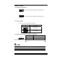
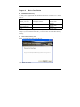
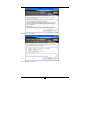
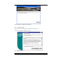
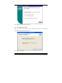
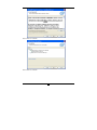
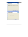
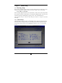
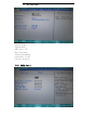
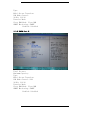
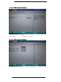
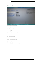
525
Network Application Platform
User’s Manual
Rev:1.0
Date:2012.03
CONTENTS
CHAPTER 1
PACKAGE CONTENTS ....................... 3 CHAPTER 2 INTRODUCTION............................ 4 CHAPTER 3 LAYOUT ................................. 5 CHAPTER 4 REAR PANEL SKETCH MAP .................. 5 CHAPTER 5 INSTALLATION........................... 6 The Interface Definition........................................................................ 6 5.1.1 Function Port Panel ............................................................ 6 5.1.2 USB Extension Interface ..................................................... 6 5.1.3 COM2-COM4 Extension Interface ................................... 6 5.1.4 LVDS Flat Panel Connector:LVDS CON ............................ 7 Jumper Settings ..................................................................................... 8 5.2.1 Jumper Presentation ............................................................ 8 5.2.2 Clear CMOS ........................................................................ 8 5.2.3 LVDS Power Selection Jumper:LCD-PWR ......................... 8 5.2.4 Inverter Power Jumper:INVERTER-PWR .......................... 8 Memory installation .............................................................................. 9 5.3.1 The system board supports One DDRIII SO-DIMM ........... 9 5.3.2 IDE Devices Installation ..................................................... 9 Other Device Installation .................................................................... 10 CHAPTER 6 DRIVER INSTALLATION ................... 12 6.1 Installation Directory ................................................................... 12 6.2 Intel Chipset Software Setup ....................................................... 12 6.3 VGA Driver Setup ........................................................................ 14 6.4 NETWORK Driver Setup ............................................................ 16 CHAPTER 7 BIOS SETUP............................. 19 1
7.1 Entering Setup .............................................................................. 19 7.2 Control keys .................................................................................. 19 7.3 The Menu Bar ............................................................................... 20 7.4 Main menu .................................................................................... 21 7.5 Advanced ....................................................................................... 22 7.6 PCIPnP .......................................................................................... 25 7.7 Boot ................................................................................................ 26 7.8 Security .......................................................................................... 26 7.9 Chipset ........................................................................................... 26 7.10 EXIT ......................................................................................... 28 CHAPTER 8 WATCHDOG PROGRAMMING INSTRUCTIONS ...... 29 Port explain .......................................................................................... 29 Example................................................................................................ 29 CHAPTER 10 ENVIRONMENT ........................... 30 2
Chapter 1
Package Contents
Your mainboard package contains the following items:
1
One D525 mainboard
2
SATA data cable
3
Drives installed CD
4
One user’s manual
3
Chapter 2
Introduction
Key Features:
-Chipset:
Intel ATOM D525 + ICH8M
-CPU:
An onboard low-power INTEL Atom® processors, main frequency
D525 as
1.80GHZ, 1MB L2 cache, supports Hyper-Threading technology, which is run at the
two thread task.
-Memory:
Supports DDR3 800 Single Channel Mode
Provides 200pin SO-DIMM DDR3 slots
-I/O :
- Provides two channel connecting two SATA drives
With speed up to 300MB/S
Four serial port
One LPT port
One VGA port
Four USB ports
-Onboard network Card
Onboard two RTL8111DL network Card
-Expansion slot:
One 32-bit PCI slots 2.3 specification compliant
One Mini PCIE port
-Power supply:
ATX standard power mode.
4
Chapter 3
Chapter 4
Layout
Rear panel sketch map
5
Chapter 5
Installation
The Interface Definition
5.1.1
Function Port Panel
FPIO1
USB Extension Interface
USB2
5.1.2
5.1.3
COM2-COM4 Extension Interface
2
10
1
9
Pin #
1
2
3
4
5
6
7
8
9
10
Signal Name
DCD, Data carrier detect
DSR, Data set ready
RXD, Receive data
RTS, Request to send
TXD, Transmit data
CTS, Clear to send
DTR, Data terminal ready
RI, Ring indicator
GND, ground
COM VCC
6
5.3.1
1
3
5
GND
TX485+/422+
RX422+
5.1.4
1
3
5
7
9
11
13
15
17
19
COM4_1
2
4
6
GND
TX485-/422RX422-
LVDS Flat Panel Connector:LVDS CON
+3.3VDC
GND
RXIN0GND
RXIN1+
RXIN2GND
RXCLK+
RXIN3GND
2
4
6
8
10
12
14
16
18
20
+3.3VDC
GND
RXIN0+
RXIN1GND
RXIN2+
RXCLKGND
RXIN3+
+5VDC
LVDS
19
20
7
Jumper Settings
5.2.1 Jumper Presentation
Pins 1 and 2 are shorted with a jumper cap.
1 2
3
Pins 2 and 3 are shorted with a jumper cap.
1 2
3
5.2.2 Clear CMOS
J1 is used to clear the CMOS Data in the RTC.
J1
Description
Normal
Clear CMOS
5.2.3 LVDS Power Selection Jumper:LCD-PWR
JP2
Pin #
MODE
1 &2short
2 &3short
+3.3V
+5V
5.2.4 COM4 RS232/422/485 Jumper:JP3
JP3
JP3
1-2
2-3
RS232 / RS422 / RS485 跳选
RS232
RS422 / RS485
8
Memory installation
5.3.1 The system board supports One DDRIII SO-DIMM
1.
Single Channel (SC)
Data will be accessed in chunks of 64 bits (8B) from the memory
channels.
2.
A DIM module simply snaps into a DIMM socket on the system
board. Pin 1 of the DIM module must correspond with Pin 1 of the
socket.
1).
Pull the “tabs” which are at the ends of the socket to the side.
2).
Position the DIMM above the socket with the “notch” in the
module aligned with the “key” on the socket.
3).
Seat the module ver tickly into the socket. Make sure it is
completely seated. The tabs will hold the DIMM in place.
5.3.2 IDE Devices Installation
IDE devices include hard disk drives, high-density diskette drives, and CD-ROM
or DVD-ROM drives, among others.
The mainboard support one or two IDE devices. If you connect two
9
devices to a single cable, you must configure one of the drives as
Master and one of the drives as Slave. The documentation of the IDE
device will tell you how to configure the device as a Master or Slave
device. The Master device connects to the end of the cable.
Other Device Installation
5.4.1 Serial ATA Installation
(7-Pin SATA1/SATA3)
The motherboard bundles the new Serial ATA technology through the SATA
interfaces onboard. The SATA specification allows for thinner, more flexible
cables with lower pin count, reduced voltage requirement. These connectors
support Serial ATA HDDs and allow up to 300MB/s data transfer rate using thin
4-conductor SATA cables. faster than the standard parallel ATA with
133MB/s(Ultra ATA/133)
Note1: The Serial ATA cable is smaller and more flexible allowing easier routing
inside the chassis. The lower pin count of the Serial ATA cable eliminates the
problem caused by the wide, flat ribbon cables of the Parallel ATA interface.
Hot plug support for Serial ATA drive and connections are not available in this
motherboard.
5.4.2 Clear CMOS (Clear RTC RAM)
This jumper allows you to clear the Real Time Clock (RTC) RAM in CMOS. You
can clear the CMOS memory of date, time, and system setup parameters by
erasing the CMOS RTC RAM data. The RAM data in CMOS, that include system
setup information such as system passwords, is powered by the onboard button
cell battery.
1、 Turn OFF the computer and unplug the power cord.
2、 Move the jumper cap from pin 1-2(default) to pin 2-3.Keep the cap on pin 2-3 for
about 5-10 seconds, and then move the cap back to pins1-2.
3、 Plug the power cord and turn ON the computer.
4、 Hold down the<F1> key during the boot process and enter BIOS setup to re-enter
data.
10
Note1: Except when clearing RTC RAM, never remove the cap on CLRTC1
jumper default position. Removing the cap will cause system boot failure!
Note2: You do not need to clear the RTC when the system hangs due to over
clocking. For system failure due to over clocking, use the C.P.R. (CPU Parameter
Recall) feature. Shut down and reboot the system so BIOS can automatically reset
parameter settings to default values.
11
Chapter 6
Driver Installation
6.1 Installation Directory
The utility CD is supplied with that mainboard the connects contained in it is showed
as below:
Directory
Driver
Inf\INF_9.2.0.1021
Intel chipset software
VGA\D410_D510
Intel onboard VGA driver
Network\Intel\intel
82574
onboard NETWORK driver
OS
Windows
2000/XP/Vista
Windows
2000/XP/Vista
Windows
2000/XP/Vista
Before installing audio driver, you must identify the mode of HD Audio codec. Fox
example: If you use Related serial codec, you need to enter into the Related directory
installing.
6.2 Intel Chipset Software Setup
Insert the driver CD, running driver software CD, choose the directory: \ CD-ROM:\
Inf\INF_9.2.0.1021\ INF_allOS_9.2.0.1021_PV
Click“NEXT”to continue
12
Select“YES” to continue
Select“NEXT” to continue
13
Select“FINISH” to complete the installation.
6.3
VGA Driver Setup
Insert the driver CD, running driver software CD, choose the
directory:\CD-ROM:\ VGA\D410_D510\
Select“Yes”to continue
14
Select“Next”to continue
Continue
15
Select“Finish”to complete the installation
6.4
NETWORK Driver Setup
Insert the driver DVD, running driver software DVD, choose the directory:
\DVD-ROM:\ Network\Intel\intel 82574\
Select“Next”to continue
16
Select“Next”to continue
Select“Next”to continue
17
Select“Install”to continue
Select “Finish”to continue
18
Chapter 7 BIOS Setup
7.1 Entering Setup
Power on the computer and the system will start POST (Power On Self Test) process.
when the message below appears on the screen, press <DEL> key to enter Setup.
Press <DEL> to run Setup
If the message disappears before you respond and you still wish to enter setup,restart
the system by turning it OFF and On or pressing the RESET button. You may also
restart the system by simultaneously pressing <Ctrl>,<Alt>,and<Delete>keys.
2.Use the arrow keys to select the item and press <Enter> to accept or enter the
sub-menu
7.2 Control keys
The BIOS setup program provides a General Help screen. You can call up this screen
from any menu by simply pressing <F1>.The Help screen lists the appropriate keys to
use and the possible selections for the highlighted item.Press <Esc> to exit the Help
screen.
19
7.3 The Menu Bar
System Time:
System Date:
SATA Port 1/2
Boot Features:
Installed memory:
Available to OS:
Used by devices:
7.3.1 SATA Port 1
20
Type:
Multi-Sector Transfers:
LBA Mode Control:
32 Bit I/O:32
Transfer Mode:
Ultra DMA Mode: Ultra DMA
SMART Monitoring: SMART
Enabled、Disabled
7.3.2 SATA Port 2
Total Sectors:
Maximum Capacity:
Type:
Multi-Sector Transfers:
LBA Mode Control: LBA
32 Bit I/O:32
Transfer Mode:
Ultra DMA Mode: Ultra DMA
SMART Monitoring: SMART
Enabled、Disabled
21
7.1.2.3 Boot Features
Summary screen:
Boot-time Diagnostic Screen:
Quick Boot Mode:
Extended Memory Testing:
Fast Boot Fine Tune:
Enabled、Disabled
7.2.3 Intel
Port 80h Cycles:
80h
Legacy USB Support:
22
7.2.3.1 CPU Control Sub-Menu
Hyperthreading:
Processor Power Management:
Enabled、Disabled
7.2.3.2 Video (Intel IGD) Control Sub-Menu
Default Primary Video Adapter:
IGD-Device 2: IGD2
IGD-Device 2, Function 1:
1
DUMT 4.0 Mode: DUMT 4.0
IGD-LCD Control Sub-Menu: IGD-LCD
23
7.2.3.3 ICH Control Sub-Menu
Port 80h Cycles:
PXE OPROM:
80h
Enabled、Disabled
7.2.3.4 LPC Control Sub-Menu
Onboard Serial Port:
24
7.2.4 Security
Supervisor Password Is:
Set:
Clear:
User Password Is:
Set:
Clear:
Set Supervisor Password:
Set User Password:
Fixed disk boot sector:
Virus check reminder:
Password on boot:
Disabled
Enabled
25
7.2.5 Power
CPU TEMP Warning: CPU
CPUFAN Fall Warning: CPU
After Power Failure:
Disable ACPI _SX
ACPI _SX
Watchdog ctrl:
Resume On Time:
Resume Time
Enabled、Disabled(
7.2.6 Boot
26
7.2.7 Exit
Exit Saving Changes:
Exit Discarding Changes:
Load Setup Defaults
Discard Changes:
Save Changes:
Exit Saving Changes
F10
27