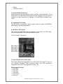
1
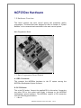
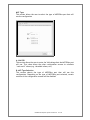
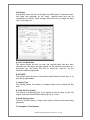
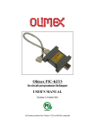
Artic Consultants Limited
MCP250xx Development System
User Manual
Version:
Release:
1.0
General Release
MCP250xx Development System User Manual 1 of 25
Project:
Date:
Time:
Location:
MCP250xx Development System
N/A
N/A
Contents
Contents ________________________________________________________ 2
Revision History__________________________________________________ 2
MCP250xx Dev-Sys Overview ______________________________________ 3
Overview ____________________________________________________ 3
Installation __________________________________________________ 3
MCP250xx Hardware______________________________________________ 4
1.0 Hardware Overview _______________________________________ 4
1.1 Main Programmer Board Details ____________________________ 4
MCP250xx Software ______________________________________________ 7
1.0 Software Overview________________________________________ 7
2.0 Software Detail ___________________________________________ 7
Programmer Operation __________________________________________ 10
Overview ___________________________________________________ 10
Reading Target MCP250xx Configuration _______________________ 10
Configuration Operation _________________________________________ 12
Overview ___________________________________________________ 12
Revision History
Issue
1
Date
14/03/07
Author
S. Allwood
Comment
First Issue
MCP250xx Development System User Manual 2 of 25
MCP250xx Dev-Sys Overview
Overview
The MPC250xx Development System allows a user to quickly and accurately
configure and Program the Microchip MCP250xx CAN expanders.
Configuration & Programming is carried out in a simple GUI interface, where
each aspect of the MCP250xx configuration is detailed.
The MCP250xx Development System will also read and write Microchips own
*.dvs file format, which ensures full forward and backward capability with
existing MCP250xx configuration files.
Installation
MCP250xx Development System will not operate without the USB driver
software first being installed. Please install the software before continuing
to use the MCP250xx Development System
Responsibilities of Operation of MCP250xx
Hardware & Software
Connecting MCP250xx hardware to an
existing CAN bus may cause errors and inoperation.
Serious Injuries and Damage to systems,
other people, equipment and the user may
result if the MCP250xx hardware is not
operated in a responsible manor.
MCP250xx Development System User Manual 3 of 25
MCP250xx Hardware
1.0 Hardware Overview
This board contains the main control system and production quality
programmer. This board has been designed to allow a number of “System
Modules” to be connected and controlled via the main control system.
Main Programmer Board
1.1 Main Programmer Board Details
A: USB2.0 Connector:
This connects the MCP250xx hardware to the PC system running the
MCP250xx Development System Software.
B: DC PSU Socket
This is the PSU socket. Connect the supplied PSU to this socket. Connecting
any other PSU to this socket could result in damage to the MCP250xx
development system hardware. The MCP250xx requires a PSU connection
with the following specifications.
o +18v dc
MCP250xx Development System User Manual 4 of 25
o 250mA
o Centre Pin Positive
C: System Module connectors
These connectors (6) are reserved to allow suitable “System Modules” to be
connected to the MCP250xx Development System hardware. No not connect
anything to these connectors or damage to the MCP250xx hardware may
result.
D: Programmer Zip Socket
This ZIF socket is provided to allow a quick connect/release of MCP250xx
parts during a programming session.
E: MCP250xx ICSP Header
This simple pin header allows the programmer to be used in an ICSP mode,
where a conventional ICSP connector cannot be used.
ICSP Pin Header Connections
F: RJ45 ICSP MCP250xx ICSP Socket.
This socket allows the programmer to be used in an ICSP mode. The use of
the “industry standard” RJ45 connector makes this ICSP connection
compatible with other ICSP programmers (ICD2, etc)
RJ45 Socket Pin Detail
o Pin1: Vpp
o Pin2: Vdd
o Pin3: Gnd
o Pin4: Data
o Pin5: Clock
o Pin6: N/C
MCP250xx Development System User Manual 5 of 25
G: Status Led’s
These Led’s allow the status of the Programmer to be understood. The Led’s
detail the following functionality;
PWR (Green): Indicates that the Main board is powered and is operating
correctly. This LED will flash slowly (1Hz) in a problem with the
programming voltage calibration has occurred.
RD (Green): Indicates when the programmer is “reading” information from
the target MCP250xx part.
WR (Yellow): Indicates when the programmer is “writing” information to
the target MCP250xx part. 2. Main Control Window
VAR (Yellow): Indicates when the programmer is verifying the programmed
information is correctly programmer. The verify process uses a Vdd of 5.5v,
5.0v and 2.7v to ensure the information is correctly programmed into the
MCP250xx.
PASS (Green): Indicates if the target MCP250xx part has been correctly
programmed and verified correctly. This indicator will remain lit until a
fresh program cycle is started.
FAIL (Red): Indicates that the target MCP250xx part failed to program and
verify correctly. This indicator will remain lit until a fresh program cycle is
started.
MCP250xx Development System User Manual 6 of 25
MCP250xx Software
1.0 Software Overview
The MCP250xx Application software provides a GUI environment to develop
MCP250xx configurations.
The software will read and write previously developed configuration files of
Microchips own *.dvs format. This gives the Artic MCP250xx Development
System full forward and backward compatibility.
The supplied software is designed to run on the following platforms. All
supported platforms operate in a similar manor.
o Microsoft Windows® XP
o Mac OS X
o Linux OS
2.0 Software Detail
2.1 Application Start
This image will be shown for five seconds while the application is starting.
Once the application has fully initialised the splash screen is removed and
the Main Programmer Screen is displayed.
MCP250xx Development System User Manual 7 of 25
2.2 Main Programmer Screen
2.3 Main Programmer Feature Description
A: File Menu.
This menu allows the user the following options.
New: Creates a new default MCP250xx configuration. The MCP25020,
MCP25025, MCP25050 & MCP25055 default parameters are supported.
o Open: Allows a user to reload a previously saved MCP250xx configuration
file. Two file formats are supported
o Save: Allows a user to save the current MCP250xx configuration settings.
Two file formats are supported
o Save As: Allows a user to save the current MCP250xx configuration
settings. The user needs to supply a valid file name. Two file formats are
supported
o Default File Types: This option allows the user to set the default file
type. The Artic MCP250xx Development System supports two file types.
Type 1: Artic Development System (*.ads).
Type 2: Microchip Development System (*.dvs). This
option is disabled if the Artic Development System
hardware has not been detected.
o Exit: Causes the application to close.
B: Configure
MCP250xx Development System User Manual 8 of 25
Communications Port: This setting allows the user to select the
communications port that will use to communicate with the
MCP250xx Development System Hardware.
C: View
Config Registers: Shows the values of the configuration registers (in
Hex and Binary formats)
I/O Visual: Shows the I/O settings of the MCP250xx
D: Options
Vdd & Vpp Calibration: Allows the user to calibrate the Vdd & Vpp values of
the programmer hardware. The actual values are shown in the “About
Screen…”
E: Help
Artic Consultants on the web: This item opens a web browser and
navigates to the Artic Consultants Ltd web site
About MCP250xx Development System: This shows hardware &
software version numbers, Programmer Calibration status and ICE
Status.
F: Read Config
This button will cause a read from the target MCP250xx EPROM memory.
G: Write Config
This button will cause a write to the target MCP250xx EPROM memory.
H: Status
This area of the screen shows details of the current Development System
operation
I: Configuration
This button opens the GUI MCP250xx configuration screen
J: ICE
This button opens the GUI In-Circuit-Emulator screen.
MCP250xx Development System User Manual 9 of 25
Programmer Operation
Overview
The programmer provides a way to read and write MCP250xx configuration
files to the OTP memory of a target MCP250xx part.
Production Quality Programmer
The programmer is a Production Quality programmer. Where the MCP250xx
part is written using an accurate 5v applied to Vdd.
The target MCP250xx part is validated at the limits of valid Vdd operation
(2.7v dc and 5.5v dc). This ensures that the configuration data is correctly
programmed and the MCP250xx part can be used with all valid Vdd voltage
settings.
Reading Target MCP250xx Configuration
This feature allows a pre-programmed MCP250xx configuration to be read
from the device.
Once the configuration has been read, an option to save the configuration to
file will be available. Also the Write Config option will be available.
Writing Target MCP250xx Configuration
MCP250xx parts are OTP (one-time-programmable). So before writing data
to the target MCP250xx, always ensure that the configuration you will be
writing is correct – errors cannot be corrected after the write process has
taken place.
This message will always be shown if a Write to target memory has been
requested
MCP250xx Development System User Manual 10 of 25
Clicking the CANCEL button will cancel the write request and return back to
the programmer main screen
Clicking the WRITE button will start the write process to the target
MCP250xx EPROM memory…
After the write process, the target MCP250xx EPROM memory is validated…
MCP250xx Development System User Manual 11 of 25
Configuration Operation
Overview
MCP250xx configuration is view easy to accomplish via the GUI Configuration
screen. Each main area of MCP250xx configuration is split and grouped
together into related areas
There are 10 main sections in the MCP250xx configuration page
o
o
o
o
o
o
o
o
o
o
MCP Type
OSC Type
CAN Engine
CAN ID
Scheduled TX
Options
GPIO Settings
ADC Settings
PWM Settings
User ID
MCP250xx Development System User Manual 12 of 25
MCP Type
This section allows the user to select the type of MCP250xx part that will
use the configuration
A: Vdd PSU
This section allows the user to enter the Vdd voltage that the MCP250xx part
will use. This value allows the other configuration screens to calculate
“real-world” values (e.g. threshold values, etc)
B: MCP Type Selection
This section selects the type of MCP250xx part that will use this
configuration. Depending on the type of MCP250xx part selected, certain
sections of the configuration screens will be disabled
MCP250xx Development System User Manual 13 of 25
OSC Type
This section allows the user to select the type of oscillator that will be used
with the MCP250xx part and allows the user to detail the speed of the
oscillator. This speed value will be other configuration sections to show
“real-world” values and times that have been selected.
A: Oscillator Configuration
This section selects the type of crystal/resonator circuit that will be used
with the MCP250xx part.
B: [Fosc] Oscillator Frequency
This section allows the user to enter the oscillator speed (in Mhz)
MCP250xx Development System User Manual 14 of 25
CAN Engine
This section allows the user to configure the CAN Engine. It features a AutoCalc Baud rate generator so the “basic” required baud rate can be
calculated very quickly. Other settings allow the user to change the baud
rate, Tq settings, etc
A: Auto-Calc Baud Rate
This section allows the user to enter the required baud rate and autocalculate the CAN engine settings needed. All the solutions are shown in a
drop-down list, and allows the user to select the “best-fit” for the
hardware/CAN bus application
B: BTLMODE
This section allows the user to have Phase Seg2 linked to Phase Seg1 or to
be freely programmable
C: Sample Type
This setting selects the number of samples taken when reading the bus
level.
D: Wake Up Filter Enable
This selects an additional filter to be applied to the Rx input of the CAN
engine, and stops the MCP250xx waking up due to “noise”.
E: Baud Rate Prescaler
This sets the BRP setting. A large value results in slower baud rates being
generated
F: Propagation Time Segment
MCP250xx Development System User Manual 15 of 25
This sets the Tq used for the Propagation time. This setting should reflect
the actual time taken by the signal to travel the length of the CAN bus
media. (E.g. a short and lightly loaded CAN bus should use a small PropSeg
value. While a long CAN bus should use a large PropSeg value)
G: Phase Buffer 1 Segment
This, together with Phase Buffer 2 Segment, sets the sample point used by
the CAN engine.
H: Phase Buffer 2 Segment
This, together with Phase Buffer 1 Segment, sets the sample point used by
the CAN engine.
I: SJW TQ
This section sets the size of the “re-sync” window.
J: Results
This shows the current selected/calculated baud rate and the error %
against the required baud rate.
MCP250xx Development System User Manual 16 of 25
CAN ID
This section allows the TX and Rx buffers to be defined, and how the
MCP250xx part responds to CAN messages. Using actual ID’s rather than
setting SID & EID bytes means that the user can quickly set the ID’s used by
the MCP250xx without the need to resort to binary to hex conversions, etc.
A: TXID0
This sets the ID used for TX Buffer 0. This buffer is used to send “Bus-On”
and scheduled transmissions. The user can select Standard or Extended
Frame type and enter the ID used in HEX format.
B: TXID1
This sets the ID used for TX Buffer 1. This buffer is used to send “Command
Ack”, “Receive Overflow” and “Error Condition” transmissions. The user can
select Standard or Extended Frame type and enter the ID used in HEX
format.
C: TXID2
This sets the ID used for “Digital I/P edge detection” and “Analog input edge
detection” transmissions. . The user can select Standard or Extended Frame
type and enter the ID used in HEX format.
D: RX Mask
This setting allows the user to limit the scope of the MCP when receiving
CAN frames. Usually this value should be set to all 1s to ensure the MCP only
responds to the required RX0 and RX1 ID values
E: RXID0
MCP250xx Development System User Manual 17 of 25
This setting allows the user to set the base CAN ID that the MCP250xx will
respond to, when data is requested from the MCP250xx. It also allows the
user to select the type of messaging used for the IRM messages.
F: RXID1
This setting allows the user to set the base CAN ID that the MCP250xx will
respond to, when data is written to the MCP250xx.
MCP250xx Development System User Manual 18 of 25
Scheduled TX
This section allows the user to set the type and speed of the scheduled TX
from the MCP250xx part.
A: Enable Scheduled Transmissions
This enables or disables the scheduled transmission from the MCP250xx part
B: Transmit A/D and GPIO Data
This setting allows the A/D and GPIO data be to added or removed from the
scheduled transmission.
C: Base Frequency
This setting selects the scheduled transmission “pre-scaler” timer value.
D: Scheduled Transmission Multiplier
This setting selects the scheduled transmission “post-scaler” timer value.
E: Scheduled Transmission Time
This shows the calculated scheduled transmission period
MCP250xx Development System User Manual 19 of 25
Options
This section allows the user to configure the various options contained
within the MCP250xx part. These options mainly deal with setting up the
required interaction of the MCP250xx and the CAN bus.
A: PUNRM
This option sets the CAN engine operation mode that will immediately run
following a successful self-configuration.
B: ERREN
This option sets how the MCP handles a “recovery from error” event
C: TXONEN
This option enables the “TX on Error Count > Threshold” CAN frame
D: SLPEN
This option sets how the MCP250xx part can enter sleep-mode
E: PUSLP
This option sets the operational mode of the CAN engine after a Wake-up
event has occurred
F: CMREQ
This option must always be enabled during a self-configuration event.
MCP250xx Development System User Manual 20 of 25
GPIO Settings
This section sets up the I/O configuration that will be used by the MCP250xx
part after a successful self-configuration
A: GPIO
This section allows the user to select the I/O pin that requires configuration
B: GPIO Pin Function
This section allows the user to select the type of I/O that will be used on
this pin. Not all I/O pins has the same functionality
C: Generate CAN Frame On Change
This section allows the user to configure which I/O pins will crate a CAN
frame on input status change or ADC threshold detected
D: Default Output Value
This section allows the user to set the default I/O state when the GPIO pin is
configured as Digital Output
E: Enable Weak Pull-Ups
This setting allows the Weak-Pullups mode to be enabled for PGIO pins
configured as digital input.
MCP250xx Development System User Manual 21 of 25
ADC Settings
This section allows the user to configure the ADC section of the MCP250XX
parts (NB. Only the MCP25050 & MCP25055 parts contain an ADC module)
A: ADC Module Main Control
This section allows the user to configure the default mode for the ADC
B: +Vref Selection
This section allows the user to input the +Vref voltage value that will be
used
C: -Vref Section
This section allows the user to input the -Vref voltage value that will be
used
D: ADC Acquisition Time
This setting allows the user to select how long the ADC module spends
reading a value before ADC conversion takes place
E: Auto Conversion Rate
This section allows the user to selects the speed of the ADC conversion
F: Auto Conversion Time
This setting allows the user to select the time the ADC module waits before
carrying out an auto conversion
G: ANA3 Threshold
This section details how the direction and level of signal to cause a
threshold detection CAN frame to be sent
MCP250xx Development System User Manual 22 of 25
H: ANA2 Threshold
This section details how the direction and level of signal to cause a
threshold detection CAN frame to be sent
I: ANA1 Threshold
This section details how the direction and level of signal to cause a
threshold detection CAN frame to be sent
J: ANA0 Threshold
This section details how the direction and level of signal to cause a
threshold detection CAN frame to be sent
MCP250xx Development System User Manual 23 of 25
PWM Settings
This section allows the user to set up the PWM outputs of the MCP250xx
part.
A: PWM1 Timer Pre-Scaler
This setting configures the default pre-scaler value
B: Period
This setting is used to program the default PWM frequency required
C: Duty Cycle
This setting is used to program the default Duty Cycle used by the PWM
generator
D: PWM1 Timer Pre-Scaler
This setting configures the default pre-scaler value
E: Period
This setting is used to program the default PWM frequency required
F: Duty Cycle
This setting is used to program the default Duty Cycle used by the PWM
generator
G: Enable PWM Default Values
This enables the PWM output to revert to the programmed default PWM
settings if the event of an error condition, etc
MCP250xx Development System User Manual 24 of 25
User ID
This section allows the user to set the user ID bytes of the MCP250xx. These
bytes do not alter the operation of the MCP; only allow the user to include
“Serial Number” and “hardware Number”, etc information. These bytes can
be read via CAN
A: Use ASCII Format
This setting allows the user to enter ASCII data into the user ID bytes of the
MCP250xx
B: User HEX Format
This setting allows the user to enter HEX value data into the user ID bytes of
the MCP250xx
C: Configuration Comment
This setting allows the user to provide a comment about this MCP250xx
configuration. (E.g. / V1.2 Config. Date: 12/5/06 Project: Dash W/L Driver)
MCP250xx Development System User Manual 25 of 25