1
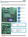
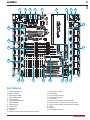
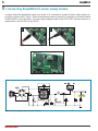
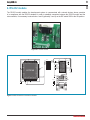
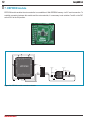
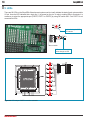
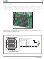
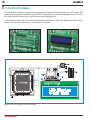
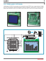
All MikroElektronika´s development systems represent irreplaceable
tools for programming and developing microcontroller-based devices.
Carefully chosen components and the use of machines of the last
generation for mounting and testing thereof are the best guarantee of
high reliability of our devices. Due to simple design, a large number of
add-on modules and ready to use examples, all our users, regardless
of their experience, have the possibility to develop their project in a fast
and efficient way.
User manual
Development system
If you have any questions, comments or business proposals, do not hesitate to contact us at [email protected]
If you are experiencing some problems with any of our products or just need additional information, please place your ticket at
www.mikroe.com/en/support
If you want to learn more about our products, please visit our website at www.mikroe.com
EasyARM v6
™
DISCLAIMER
All the products owned by MikroElektronika are protected by copyright law and international copyright treaty.
Therefore, this manual is to be treated as any other copyright material. No part of this manual, including
product and software described herein, may be reproduced, stored in a retrieval system, translated or
transmitted in any form or by any means, without the prior written permission of MikroElektronika. The
manual PDF edition can be printed for private or local use, but not for distribution. Any modification of this
manual is prohibited.
TO OUR VALUED CUSTOMERS
I want to express my thanks to you for being interested in our products and for having confidence in
Mikroelektronika.
The primary aim of our company is to design and produce high quality electronic products and to constantly
improve the performance thereof in order to better suit your needs.
Nebojsa Matic
General Manager
MikroElektronika provides this manual ‘as is’ without warranty of any kind, either expressed or implied,
including, but not limited to, the implied warranties or conditions of merchantability or fitness for a particular
purpose.
MikroElektronika shall assume no responsibility or liability for any errors, omissions and inaccuracies that may
appear in this manual. In no event shall MikroElektronika, its directors, officers, employees or distributors be
liable for any indirect, specific, incidental or consequential damages (including damages for loss of business
profits and business information, business interruption or any other pecuniary loss) arising out of the use
of this manual or product, even if MikroElektronika has been advised of the possibility of such damages.
MikroElektronika reserves the right to change information contained in this manual at any time without prior
notice, if necessary.
HIGH RISK ACTIVITIES
The products of MikroElektronika are not fault – tolerant nor designed, manufactured or intended for use or
resale as on – line control equipment in hazardous environments requiring fail – safe performance, such as
in the operation of nuclear facilities, aircraft navigation or communication systems, air traffic control, direct
life support machines or weapons systems in which the failure of Software could lead directly to death,
personal injury or severe physical or environmental damage (‘High Risk Activities’). MikroElektronika and its
suppliers specifically disclaim any expressed or implied warranty of fitness for High Risk Activities.
TRADEMARKS
The Mikroelektronika name and logo, the Mikroelektronika logo, mikroC, mikroC PRO, mikroBasic, mikroBasic PRO, mikroPascal, mikroPascal PRO, AVRflash, PICflash, dsPICprog, 18FJprog, PSOCprog, AVRprog, 8051prog, ARMflash, EasyPIC5, EasyPIC6, BigPIC5, BigPIC6, dsPIC PRO4, Easy8051B, EasyARM,
EasyAVR5, EasyAVR6, BigAVR2, EasydsPIC4A, EasyPSoC4, EasyVR Stamp LV18FJ, LV24-33A, LV32MX,
PIC32MX4 MultiMedia Board, PICPLC16, PICPLC8 PICPLC4, SmartGSM/GPRS, UNI-DS are trademarks
of Mikroelektronika. All other trademarks mentioned herein are property of their respective companies.
All other product and corporate names appearing in this manual may or may not be registered trademarks
or copyrights of their respective companies, and are only used for identification or explanation and to the
owners’ benefit, with no intent to infringe.
The NXP name, logo and products names are trademarks of NXP Inc. in the U.S.A and other countries.
©MikroelektronikaTM, 2011 All Rights Reserved.
3
page
EasyARM v6
TABLE OF CONTENTS
General information .......................................................................................................................... 4
Key features ..................................................................................................................................... 5
1. Connecting EasyARM v6 to power supply module ...................................................................... 6
2. Connecting EasyARM v6 to a PC ................................................................................................ 7
3. USB UART1 and USB UART2 modules ...................................................................................... 8
4. RS-232 module ............................................................................................................................. 9
5. Piezo buzzer ................................................................................................................................10
6. CAN module .................................................................................................................................11
7. EEPROM module .........................................................................................................................12
8. USB communication ....................................................................................................................13
9. LEDs ............................................................................................................................................14
10. Push buttons ..............................................................................................................................15
11. 2x16 LCD display .......................................................................................................................16
12. 128x64 graphic display ..............................................................................................................17
13. Touch panel ................................................................................................................................19
14. I/O ports .....................................................................................................................................20
MikroElektronika
page
4
EasyARM v6
General information
The EasyARM v6 development system provides a development environment for programming and experimenting with
ARM microcontrollers from NXP®. Numerous modules, such as 128x64 graphic LCD display, 2x16 alphanumeric LCD
display, piezo buzzer, CAN, etc. are provided on the board and allow you to easily simulate the operation of your target
device.
Full-featured development
system for ARM
microcontroller based devices
UART communication via
USB connector
CAN communication module
Integrated EEPROM module
Graphic LCD display with
backlight
Package includes:
Development system:
CD:
Cables:
Documentation:
EasyARM v6
product CD with relevant software
USB cable
manual and electrical schematic for EasyARM v6
System specification:
Power supply:
Power consumption:
Dimensions:
Weight:
MikroElektronika
over AC/DC connector (7-23V AC or 9-32V DC)
or a USB cable (5V DC)
50mA when all on-board modules are off
26,5 x 22cm (10,4 x 8,6inch)
~420g (0.92lbs)
5
1
2
3
4
5
6
7
8
page
EasyARM v6
9
10
23
22
11
21
20
19 18
17
16
15
14 13 12
Key features
1. Power supply module
2. AC/DC connector
3. USB UART1 module
4. USB UART2 module
5. RS-232 module
6. mikroARM board socket
7. Serial EEPROM
8. USB connector
9. CAN module
10. Piezo buzzer
11. I/O ports
12. Jumpers used to select pull-up/pull-down resistors
13. Touch panel controller
14. DIP switches
15. GLCD display connector
16. Touch panel connector
17. Push buttons
18. Jumper used to shorten protective resistor
19. Jumpers used to select push buttons’ logic state
20. Jumpers used to select pull-up/pull-down resistors
21. LEDs
22. I/O ports
23. LCD display connector
MikroElektronika
page
6
EasyARM v6
1. Connecting EasyARM v6 to power supply module
In order to enable the development system to be turned on, it is necessary to provide the power supply voltage over
an AC/DC connector CN37, Figure 1. When the development system is powered, it is necessary to set switch marked
POWER SUPPLY to the ON position. The power supply voltage provided via the CN37 AC/DC connector may be in a
range between 7 and 23V AC or 9 and 32V DC.
2
1
Figure 1-1: Powering the development system
Figure 1-2: Power supply module
Figure 1-3: Power supply module connection schematic
MikroElektronika
7
page
EasyARM v6
2. Connecting EasyARM v6 to a PC
The EasyARM v6 development system comes with the mikroBoard for ARM provided with a USB connector. This
connector enables the development system to be connected to a PC. It is also possible to provide the system with
the 5V power supply voltage from the PC via this connector. The mikroBoard for ARM may be used as a stand-alone
device. When connecting the mikroBoard for ARM card to the development system, it is necessary to remove jumper
marked STANDALONE. For more information on the mikroBoard for ARM, refer to the relevant manual.
1
2
Figure 2-1: Connecting the development system to a PC
Figure 2-2: mikroBoard for ARM
In addition to the mikroBoard for ARM, the development system can also be connected to a PC via USB UART 1 or
USB UART2 module supplied on the development system or via a USB connector used for USB communication. It’s
also possible to connect development system via RS-232 port.
MikroElektronika
EasyARM v6
3. USB UART1 i USB UART2 modules
USB UART modules enables the EasyARM v6 development system to be connected to a PC via a USB connector. In
addition to PC, the development system can also be easily connected to other devices that use USB communication.
USB UART modules are connected to the microcontroller supplied on the development system via P0.1(RX) and
P0.0(TX) pins for USB UART1 or P0.9(RX) and P0.8(TX) for USB UART2.
In order to establish connection between the USB UART1 module and the
microcontroller, it is necessary to set switches 5 and 6 on the DIP switch SW2 to
the ON position. To connect the USB UART2 module and the microcontroller, it is
necessary to set swiches 7 and 8 on the DIP switch SW2 to the ON position.
Figure 3-1: USB UART modules
SW2
P0.31
P1.16
LPC2148
VBAT
P1.27
P0.21
P0.22
RTXC1
P1.19
RTXC2
GND
VCCA
P1.18
P0.25
D+
DP1.17
P0.28
P0.29
P0.30
VREF
XTAL1
XTAL2
P1.28
GNDA
P0.23
RESET
P1.29
P0.20
P0.19
P0.18
P1.30
VCC3
GND
U3
P0.1
P0.0
P0.9
P0.8
VCC-5V
VCC-3.3
DTR#
OSCI
C4
C5
RTS#
TEST
100nF
100nF
VCCIO
AGND
TXD
VCC-3.3
P1.20
P0.17
P0.16
P0.15
P1.21
VCC3
GND
P0.14
P1.22
P0.13
P0.12
P0.11
P1.23
P0.10
P0.9
P0.8
RX-FTDI1
TX-FTDI1
RX-FTDI2
TX-FTDI2
RXD
VCC3
OSCO
NC
RI#
CBUS1
GND
CBUS1
NC
DSR#
VCC
RESET#
VCC-5V
VCC-5V
E5
GND
DCD#
CTS#
GND
P0.0
P1.31
P0.1
P0.2
VCC3
P1.26
GND
P0.3
P0.4
P1.25
P0.5
P0.6
P0.7
P1.24
page
8
10uF
R18
4K7
GND
CBUS4
3V3OUT
CBUS2
USBDM
CBUS3
USBDP
FT232RL
VCC
DD+
GND
USB B
R19
10K
C3
CN34
DVCC
D+ GND
100nF
Bottom view
U4
VCC-5V
VCC-3.3
DTR#
OSCI
C7
C8
RTS#
TEST
100nF
100nF
VCCIO
AGND
TXD
VCC-3.3
RXD
OSCO
NC
RI#
CBUS1
GND
CBUS1
NC
DSR#
VCC
RESET#
CTS#
10uF
R20
4K7
GND
CBUS4
3V3OUT
CBUS2
USBDM
CBUS3
USBDP
FT232RL
E6
GND
DCD#
VCC-5V
VCC-5V
VCC
DD+
GND
C6
USB B
DVCC
D+ GND
100nF
R21
10K
CN35
Bottom view
Figure 3-2: USB UART module connection schematic
MikroElektronika
9
page
EasyARM v6
4. RS-232 module
The RS-232 module enables the development system to communicate with external devices whose operation
is in compliance with the RS-232 standard. In order to establish connection between the RS-232 module and the
microcontroller, it is necessary to set switches 1 and 2 (optionally 3 and 4) on the DIP switch SW2 to the ON position.
RX232
TX232
Figure 4-1: RS-232 module
VCC-3.3
U4
LPC2148
VBAT
P1.27
P1.16
P0.31
P0.22
RTXC1
P1.19
RTXC2
GND
VCCA
P1.18
P0.25
D+
DP1.17
P0.28
P0.29
P0.30
P1.20
P0.17
P0.16
P0.15
P1.21
VCC3
GND
P0.14
P1.22
P0.13
P0.12
P0.11
P1.23
P0.10
P0.9
P0.8
RX232
TX232
C10
100nF
C1+
VCC
V+
GND
C1C12
100nF
C13
100nF
VCC3
R1 IN
C2-
R1 OUT
V-
R2 IN
C11
100nF
T1 OUT
C2+
T1 IN
T2 OUT
T2 IN
R2 OUT
R26
100K
MAX3232
GND
P0.0
P1.31
P0.1
P0.2
VCC3
P1.26
GND
P0.3
P0.4
P1.25
P0.5
P0.6
P0.7
P1.24
P0.21
VREF
XTAL1
XTAL2
P1.28
GNDA
P0.23
RESET
P1.29
P0.20
P0.19
P0.18
P1.30
VCC3
GND
SW1
P0.1
P0.0
P0.9
P0.8
VCC-3.3
1
5
6
9
CN39
VCC-3.3
E4
RS-232
SUB-D 9p
10uF
9
5
6
1
Bottom view
Figure 4-2: RS-232 module connection schematic
MikroElektronika
page
10
EasyARM v6
5. Piezo buzzer
Due to a built-in piezo buzzer, the EasyARM v6 development system is capable of emitting audio signals. In order
to enable the piezo buzzer to operate properly it is necessary to generate a voltage signal of specific frequency.
Remember, when writing the code for voltage signal generation, that the piezo buzzer’s resonant frequency is 3.8kHz.
Other frequencies in the range between 20Hz and 20kHz can also be used, but the best performance is provided with
frequencies ranging between 2kHz and 4kHz. To establish connection between the piezo buzzer and the microcontroller,
it is necessary to set switch 6 on the DIP switch SW1 to the ON position.
Figure 5-1: Piezo buzzer
Figure 5-2: Piezo buzzer connection schematic
MikroElektronika
11
page
EasyARM v6
6.0. CAN module
CAN (Controller Area Network) is a communication standard primarily intended for use in automotive industry. It
enables the microcontroller to communicate to a device installed in cars without using a host PC. In addition, this
communication is widely used in industrial automation. The EasyARM v6 development system features CAN module
used for communication with CAN devices. To establish connection between this module and the microcontroller, it is
necessary to set switches 1 and 2 (optionally 3 and 4) on the DIP switch SW3 to the ON position.
Figure 6-1: CAN module
Figure 6-2: CAN module connector
VCC-5V
R5
10
U2
MCU
P0.25
TD1
P0.23
P0.24
SW3
TXD
GND
VCC
RXD
RX-CAN
TX-CAN
RX-CAN
TX-CAN
Rs
CANH
CANL
Vref
CANH
CN40
CANL
MCP2551
VCC-5V
C2
100nF
Figure 6-3: CAN module connection schematic
MikroElektronika
EasyARM v6
7. EEPROM module
EEPROM module enables the microcontroller to use additional 1Kbit EEPROM memory via I2C serial connection. To
establish connection between this module and the microcontroller, it is necessary to set switches 7 and 8 on the DIP
switch SW1 to the ON position.
P1.27
VBAT
VREF
XTAL1
XTAL2
P1.28
GNDA
P0.23
RESET
P1.29
P0.20
P0.19
P0.18
P1.30
VCC3
GND
Figure 7-1: EEPROM module
P0.21
P0.22
RTXC1
P1.19
RTXC2
GND
VCCA
P1.18
P0.25
D+
DP1.17
P0.28
P0.29
P0.30
P0.31
P1.16
LPC2148
P1.20
P0.17
P0.16
P0.15
P1.21
VCC3
GND
P0.14
P1.22
P0.13
P0.12
P0.11
P1.23
P0.10
P0.9
P0.8
GND
P0.0
P1.31
P0.1
P0.2
VCC3
P1.26
GND
P0.3
P0.4
P1.25
P0.5
P0.6
P0.7
P1.24
page
12
VCC3
SW1
VCC-3.3
VCC-3.3
U6
P0.2
P0.3
EEPROM-SCL
EEPROM-SDA
C9
100nF
A0
A1
A2
GND
24AA01
Figure 7-2: EEPROM module connection schematic
MikroElektronika
VCC
WP
SCL
SDA
R24
1K
R25
1K
EEPROM-SCL
EEPROM-SDA
13
page
EasyARM v6
8. USB communication
The EasyARM v6 development system can communicate with external devices via the USB connector used for USB
communication. The USB connector is directly connected to the microcontroller pins used for USB communication.
Figure 8-1: USB connector of B type
VCC
DD+
GND
CN36
VCC
USB-VBUS
USB-DN
USB-DP
D-
P3.17
P3.19
P3.21
P3.23
P3.25
P3.27
P3.29
P3.31
USB B
USB-VBUS
USB-DP
D+ GND
P3.16
P3.18
P3.20
P3.22
P3.24
P3.26
P3.28
P3.30
Bottom view
USB-DN
CN32
Figure 8-2: USB connector connection schematic
MikroElektronika
page
14
EasyARM v6
9. LEDs
There are 80 LEDs on the EasyARM v6 development system used to visually indicate the state of each microcontroller
I/O pin. An active LED indicates that a logic one (1) is present on the pin. In order to enable LEDs to illuminate, it is
necessary to select the appropriate port (PORT0, PORT1 or PORT2) by using DIP switch SW1. Port PORT3 is not
connected to LEDs.
Notch indicating the SMD
LED cathode
Microcontroller
Figure 9-1: LEDs
Figure 9-2: LED and port PORT0 connection schematic
MikroElektronika
SMD resistor used to limit
current through an LED
15
page
EasyARM v6
10. Push buttons
The logic level of all microcontroller input pins may be changed by using push buttons. Jumper J17 is used to determine
the logic level to be supplied on the appropriate microcontroller pin by pressing a push button. The function of the protective resistor is to limit the maximum current, thus preventing the development system and peripheral modules from being
damaged in case a short circuit occurs. If needed, advanced users may shorten this resistor by using jumper J16.
Figure 10-1: Push buttons
By pressing any push button when jumper J17 is in the VCC-3.3 position, a logic one (3.3V) will be applied to the appropriate microcontroller pin, as shown in Figure 2.
Figure 10-2: Push buttons and port PORT0 connection schematic
MikroElektronika
page
16
EasyARM v6
11.0. 2x16 LCD display
The EasyARM v6 development system features an on-board connector for the alphanumeric 2x16 LCD display. This
connector is linked to the microcontroller via port PORT0. Potentiometer P1 is used to adjust display contrast. The LCDBCK switch on the DIP switch SW1 is used to turn the display backlight on/off.
Communication between this LCD and the microcontroller is performed in a 4-bit mode. Alphanumeric digits are displayed in two lines each containing up to 16 characters of 7x5 pixels.
Figure 11-1: Connector for alphanumeric LCD display
Figure 11-3: 2x16 LCD display connection schematic
MikroElektronika
Figure 11-2: Alphanumeric 2x16 LCD display
17
page
EasyARM v6
12.0. 128x64 graphic LCD display
128x64 graphic LCD (GLCD) is connected to the microcontroller via port PORT0. It has a screen resolution of 128x64
pixels, which allows diagrams, tables and other graphic contents to be displayed. Potentiometer P2 is used for the GLCD
display contrast adjustment. Switch 5 (GLCD-BCK) on the DIP switch SW1 is used to turn the display backlight on/off.
Figure 12-1: GLCD display
Figure 12-2: GLCD connector
Figure 12-3: GLCD display connection schematic
MikroElektronika
EasyARM v6
13.0. Touch panel
A touch panel is a thin, self-adhesive, transparent, touch-sensitive panel. It is placed over a GLCD display. Its main function
is to register pressure at some specific display point and to forward its coordinates in the form of analog voltage to the
microcontroller. Switches 5, 6, 7 and 8 on the DIP switch SW3 are used to connect the microcontroller and touch panel.
A
B
C
D
Figure 13-1: Placing touch panel over a GLCD
Figure 1 shows how to place a touch panel over a GLCD display. Make sure that the flat cable is to the left of the GLCD,
as shown in Figure 1D.
VCC
Q3
BC846
R8
1K
RIGHT
R11
10K
VCC
CN38
BOTTOM
LEFT
DRIVEA
DRIVEB
Q4
BC856
R10
10K
TOP
GLCD
RIGHT
TOP
LEFT
BOTTOM
C14
100nF
LEFT
Q2
BC846
R16
100K
VCC
C15
100nF
Q6
BC846
R17
100K
P0.21
P0.22
RTXC1
P1.19
RTXC2
GND
VCCA
P1.18
P0.25
D+
DP1.17
P0.28
P0.29
P0.30
P1.16
R9
10K
BOTTOM
P0.29
P0.30
P0.12
P0.13
VBAT
P1.27
VCC
R12
1K
R13
10K
P0.31
Q5
BC856
VREF
XTAL1
XTAL2
P1.28
GNDA
P0.23
RESET
P1.29
P0.20
P0.19
P0.18
P1.30
VCC3
GND
SW3
20
P1.20
P0.17
P0.16
P0.15
P1.21
VCC3
GND
P0.14
P1.22
P0.13
P0.12
P0.11
P1.23
P0.10
P0.9
P0.8
LPC2148
VCC3
GND
P0.0
P1.31
P0.1
P0.2
VCC3
P1.26
GND
P0.3
P0.4
P1.25
P0.5
P0.6
P0.7
P1.24
1
CS1
CS2
GND
VCC
Vo
RS
R/W
E
D0
D1
D2
D3
D4
D5
D6
D7
RST
Vee
LED+
LED-
page
18
R14
1K
R15
10K
TOUCHPANEL
CONTROLLER
Figure 13-2: Touch panel connection schematic
A
B
C
D
Figure 13-3: Connecting touch panel
Figure 3 shows in detail how to connect a touch panel to the microcontroller. Bring the end of the flat cable close to
the CN38 connector (Figure A). Plug the cable into the connector (Figure B) and press it easily so as to fully fit the
connector (Figure C). Now, a GLCD can be plugged into the appropriate connector (Figure D).
NOTE: LEDs and pull-up/pull-down resistors on port PORT0 should be off when the touch panel is in use.
MikroElektronika
19
page
EasyARM v6
14.0. Input/output ports
Along the left and right sides of the development system, there are fifteen 10-pin connectors linked to the microcontroller
I/O ports. Due to jumpers J1-J15, pull-up or pull-down resistors can be connected to I/O ports.
Figure 14-3: J9 in pulldown position
Figure 14-1: I/O ports
Figure 14-2: I/O ports
Figure 14-4: J9 in pull-up
position
Figure 14-5: Port PORT0 connection schematic
MikroElektronika
EasyARM v6
Pull-up/pull-down resistors enable you to feed all microcontroller’s input pins the logic level on when they are in idle
state. This level depends on the position of the pull-up/pull-down jumper. The P0.0 pin with the relevant jumper J2 and
P0.0 push button with jumper J17 are used here for the purpose of explaining the performance of pull-up/pull-down
resistors. The principle of their operation is the same for all other microcontroller pins.
P0.21
P0.31
P1.16
LPC2148
P0.17
P0.16
P0.15
P1.21
VCC3
GND
P0.14
P1.22
P0.13
P0.12
P0.11
P1.23
P0.10
P0.9
P0.8
RN2
8x10K
J2
VCC3
VCC-3.3
J17
P0.14
J16
R27
220
GND
P0.0
P1.31
P0.1
P0.2
VCC3
P1.26
GND
P0.3
P0.4
P1.25
P0.5
P0.6
P0.7
P1.24
P0.22
RTXC1
P1.19
RTXC2
GND
VCCA
P1.18
P0.25
D+
DP1.17
P0.28
P0.29
P0.30
P1.20
P0.14
P1.27
VBAT
VREF
XTAL1
XTAL2
P1.28
GNDA
P0.23
RESET
P1.29
P0.20
P0.19
P0.18
P1.30
VCC3
GND
VCC-3.3
up
pull
down
3.3V
In order to enable the PORT0 port pins to
be connected to pull-down resistors, it is
necessary to place jumper J1 in the Down
position first. This enables any PORT0 port
pin to be supplied with a logic zero (0V)
in idle state over jumper J2 and 8x10k
resistor network.
As a result, every time you press the P0.0
push button, the P0.0 pin will be fed with
a logic one (VCC-3.3 voltage), provided
that jumper J17 is placed in the VCC-3.3
position.
0V
Figure 14-6: Jumper J2 in pull-down and jumper J17 in pull-up position
P0.21
P0.22
RTXC1
P1.19
RTXC2
GND
VCCA
P1.18
P0.25
D+
DP1.17
P0.28
P0.29
P0.30
P0.31
P1.16
LPC2148
P1.20
P0.17
P0.16
P0.15
P1.21
VCC3
GND
P0.14
P1.22
P0.13
P0.12
P0.11
P1.23
P0.10
P0.9
P0.8
RN2
8x10K
J2
VCC-3.3
P0.14
P1.27
VBAT
VREF
XTAL1
XTAL2
P1.28
GNDA
P0.23
RESET
P1.29
P0.20
P0.19
P0.18
P1.30
VCC3
GND
VCC-3.3
up
pull
down
VCC3
J17
P0.14
J16
R27
220
GND
P0.0
P1.31
P0.1
P0.2
VCC3
P1.26
GND
P0.3
P0.4
P1.25
P0.5
P0.6
P0.7
P1.24
page
20
In order to enable port PORT0 pins to be
connected to pull-up resistors and the port
input pins to be supplied with a logic zero
(0), it is necessary to place jumper J2 in
the Up position and jumper J17 in the GND
position. This enables any port PORT0
input pin, when it is in idle state, to be
driven high (3.3V) over the 10k resistor.
As a result, every time you press the P0.0
push button, the P0.0 pin will be fed with a
logic zero (0V)
3.3V
0V
Figure 14-7: Jumper J2 in pull-up and jumper J17 in pull-down position
In case that jumpers J2 and J17 are in the
same positions, pressure on any button will
not cause input pins to change their logic
state.
Figure 14-8: Jumpers J2 and J17 in the same positions
MikroElektronika
21
page
EasyARM v6
mikroBoard for ARM 64-pin
MikroElektronika
22
page
EasyARM v6
mikroBoard for ARM 144-pin
MikroElektronika
DISCLAIMER
All the products owned by MikroElektronika are protected by copyright law and international copyright treaty.
Therefore, this manual is to be treated as any other copyright material. No part of this manual, including
product and software described herein, may be reproduced, stored in a retrieval system, translated or
transmitted in any form or by any means, without the prior written permission of MikroElektronika. The
manual PDF edition can be printed for private or local use, but not for distribution. Any modification of this
manual is prohibited.
TO OUR VALUED CUSTOMERS
I want to express my thanks to you for being interested in our products and for having confidence in
Mikroelektronika.
The primary aim of our company is to design and produce high quality electronic products and to constantly
improve the performance thereof in order to better suit your needs.
Nebojsa Matic
General Manager
MikroElektronika provides this manual ‘as is’ without warranty of any kind, either expressed or implied,
including, but not limited to, the implied warranties or conditions of merchantability or fitness for a particular
purpose.
MikroElektronika shall assume no responsibility or liability for any errors, omissions and inaccuracies that may
appear in this manual. In no event shall MikroElektronika, its directors, officers, employees or distributors be
liable for any indirect, specific, incidental or consequential damages (including damages for loss of business
profits and business information, business interruption or any other pecuniary loss) arising out of the use
of this manual or product, even if MikroElektronika has been advised of the possibility of such damages.
MikroElektronika reserves the right to change information contained in this manual at any time without prior
notice, if necessary.
HIGH RISK ACTIVITIES
The products of MikroElektronika are not fault – tolerant nor designed, manufactured or intended for use or
resale as on – line control equipment in hazardous environments requiring fail – safe performance, such as
in the operation of nuclear facilities, aircraft navigation or communication systems, air traffic control, direct
life support machines or weapons systems in which the failure of Software could lead directly to death,
personal injury or severe physical or environmental damage (‘High Risk Activities’). MikroElektronika and its
suppliers specifically disclaim any expressed or implied warranty of fitness for High Risk Activities.
TRADEMARKS
The Mikroelektronika name and logo, the Mikroelektronika logo, mikroC, mikroC PRO, mikroBasic, mikroBasic PRO, mikroPascal, mikroPascal PRO, AVRflash, PICflash, dsPICprog, 18FJprog, PSOCprog, AVRprog, 8051prog, ARMflash, EasyPIC5, EasyPIC6, BigPIC5, BigPIC6, dsPIC PRO4, Easy8051B, EasyARM,
EasyAVR5, EasyAVR6, BigAVR2, EasydsPIC4A, EasyPSoC4, EasyVR Stamp LV18FJ, LV24-33A, LV32MX,
PIC32MX4 MultiMedia Board, PICPLC16, PICPLC8 PICPLC4, SmartGSM/GPRS, UNI-DS are trademarks
of Mikroelektronika. All other trademarks mentioned herein are property of their respective companies.
All other product and corporate names appearing in this manual may or may not be registered trademarks
or copyrights of their respective companies, and are only used for identification or explanation and to the
owners’ benefit, with no intent to infringe.
The NXP name, logo and products names are trademarks of NXP Inc. in the U.S.A and other countries.
©MikroelektronikaTM, 2011 All Rights Reserved.
All MikroElektronika´s development systems represent irreplaceable
tools for programming and developing microcontroller-based devices.
Carefully chosen components and the use of machines of the last
generation for mounting and testing thereof are the best guarantee of
high reliability of our devices. Due to simple design, a large number of
add-on modules and ready to use examples, all our users, regardless
of their experience, have the possibility to develop their project in a fast
and efficient way.
User manual
Development system
If you have any questions, comments or business proposals, do not hesitate to contact us at [email protected]
If you are experiencing some problems with any of our products or just need additional information, please place your ticket at
www.mikroe.com/en/support
If you want to learn more about our products, please visit our website at www.mikroe.com
mikroBoard for ARM 64-pin
™