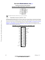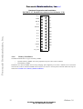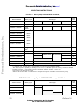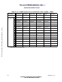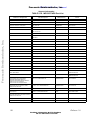
1
Freescale Semiconductor, Inc. User’s Manual Freescale Semiconductor, Inc... MPC852TADSRM/D Version 1.0 June 1, 2003 MPC852TADS User’s Manual © Motorola, Inc., 2003 For More Information On This Product, Go to: www.freescale.com Freescale Semiconductor, Inc. Important Notice to Users Freescale Semiconductor, Inc... While every effort has been made to ensure the accuracy of all information in this document, Motorola assumes no liability to any party for any loss or damage caused by errors or omissions or by statements of any kind in this document, its updates, supplements, or special editions, whether such errors are omissions or statements resulting from negligence, accident, or any other cause. Motorola further assumes no liability arising out of the application or use of any information, product, or system described herein: nor any liability for incidental or consequential damages arising from the use of this document. Motorola disclaims all warranties regarding the information contained herein, whether expressed, implied, or statutory, including implied warranties of merchantability or fitness for a particular purpose. Motorola makes no representation that the interconnection of products in the manner described herein will not infringe on existing or future patent rights, nor do the descriptions contained herein imply the granting or license to make, use or sell equipment constructed in accordance with this description. Trademarks This document includes these trademarks: Motorola and the Motorola logo are registered trademarks of Motorola, Inc. Windows is a registered trademark of Microsoft Corporation in the U.S. and other countries. Intel is a registered trademark of Intel Corporation. Motorola, Inc., is an Equal Opportunity / Affirmative Action Employer. For an electronic copy of this book, visit Motorola’s web site at http://e-www.motorola.com/ © Motorola, Inc., 2002; All Rights Reserved MPC852TADS - Version 1.0 User’s Manual MOTOROLA For More Information On This Product, Go to: www.freescale.com Freescale Semiconductor, Inc. 1 - Hardware Preparation 1•1 Jumpers and Dip-Switches Ensure the following jumpers are in place: TABLE 1-1. Default Jumpers and dip switches settings Freescale Semiconductor, Inc... Reference Name 1•2 Description Default J1 Clock Oscillator source: 1-2: 10MHz on board clock oscillator. 2-3: External clock oscillator. 1-2: 10MHz on board clock oscillator. SW1 Power Switch ON/OFF Power Switch OFF SW4 Modin Selector: Modin[1..2] = ‘OFF,ON’ Modin[1..2] : ‘OFF,ON’ = ‘1,0’ SW5 S/W Options[4..1]: ‘ON,ON,ON,ON’ S/W Option[4..1]: ‘ON,ON,ON,ON’=’0000’ Connections Connect the following connectors : • P16 - Power Supply 5.0V DC. • P13 - Power Supply 12.0V DC for PCMCIA channel or for Flash Programming. • P12 - BDM Connector via External Command Converter to Host Computer Parallel Port. • P17A (Down) - RS232-1 Connector to Host Computer COM1 Port. 1•3 Run • MOTOROLA Turn on the 5V power supply and verify LD8, LD14, LD15, LD17, LD18 Leds on board lit up. MPC852TADS - Quick Start User’s Manual For More Information On This Product, Go to: www.freescale.com -A Freescale Semiconductor, Inc... Freescale Semiconductor, Inc. MOTOROLA MPC852TADS - Quick Start User’s Manual For More Information On This Product, Go to: www.freescale.com -B FreescaleMPC852TADS Semiconductor, - User’sInc. Manual Freescale Semiconductor, Inc... Table Of Contents General Information MPC852TADS Introduction and Goals List of Abbreviations Related Documentation SPECIFICATIONS MPC852TADS Features Hardware Preparation and Installation INTRODUCTION UNPACKING INSTRUCTIONS HARDWARE PREPARATION MPC Replacement of U1 Clock Source Selection - J1 Modin Selection - SW4 Software Option - SW5 INSTALLATION INSTRUCTIONS Host Controlled Operation Standalone Operation 10/100-Base-T Ethernet Ports Connection - P9, P10 BDM Debug Port Connector - P12 +12V Power Supply Connection - P13 +5V Power Supply Connection - P16 Terminal to MPC852TADS RS-232 Connection - P17 Parallel Host Connector in EPP I/F - P20 Memory Installation OPERATING INSTRUCTIONS INTRODUCTION CONTROLS AND INDICATORS ABORT Switch, SW2 SOFT RESET Switch, SW3 HARD RESET Switches, SW2 & SW3 Modin Selection, SW4 Software Options Switch, SW5 Power-On RESET Switch, SW6 GND Bridges Ethernet 10Base-T. ETH TX/RX, LD1 Ethernet Full Duplex Indicator, LD2 Ethernet LINK Indicator, LD3 Fast Ethernet 100Mbps Indicator, LD4 Fast Ethernet 10/100Base-T. TX/RX, LD5 Fast Ethernet Full Duplex Indicator, LD6 Fast Ethernet LINK Indicator, LD7 Ethernet 10Base-T. ETH ON, LD8 RS232 Port 2 ON, LD9 I For More Information On This Product, Go to: www.freescale.com 1 1 1 1 1 3 5 5 5 5 8 8 8 9 10 10 11 12 12 12 13 13 14 15 17 17 17 17 17 17 17 17 17 18 18 18 18 18 18 18 18 19 19 Release 1.0 Freescale Semiconductor, Inc... FreescaleMPC852TADS Semiconductor, - User’sInc. Manual Fast Ethernet 10/100Base-T. ON, LD10 RS232 Port 1 ON, LD12 PCMCIA ON, LD13 FLASH ON, LD14 DRAM ON, LD15 SGLAMP ON, LD16 SDRAM ON, LD17 5V Indicator, LD18 RUN Indicator, LD19 EPP Indicator, LD20 SPP Indicator, LD21 MEMORY MAP MPC Register Programming Memory Controller Registers Programming Functional Description Reset & Reset - Configuration Regular Power - On Reset Manual Soft Reset Manual Hard Reset Host Hard Reset through on board command converter MPC Internal Sources Reset Configuration Power On Reset Configuration Hard Reset Configuration Soft Reset Configuration Local Interrupter Clock Generator Buffering Chip - Select Generator DRAM DRAM 16-Bit Operation DRAM Performance Figures Refresh Control Variable Bus-Width Control Flash Memory SIMM Synchronous DRAM SDRAM Programming SDRAM Initializing Procedure SDRAM Refresh Communication Ports RS232 Ports RS232 Port Signal Descriptions Ethernet Port FETHC - Fast Ethernet Controller on Port - D DM9161E Control PCMCIA Port II For More Information On This Product, Go to: www.freescale.com 19 19 19 19 19 19 20 20 20 20 20 20 22 23 34 34 34 34 34 34 35 35 35 35 36 36 36 36 37 37 38 38 39 40 42 43 46 47 47 48 48 48 48 48 49 49 Release 1.0 Freescale Semiconductor, Inc... FreescaleMPC852TADS Semiconductor, - User’sInc. Manual PCMCIA Power Control Board Control & Status Register: BCSR BCSR0: Hard Reset Configuration Register BCSR1: Board Control Register 1 BCSR2: Board Control / Status Register 2 BCSR3: Board Control / Status Register 3 BCSR4 - Board Control / Status Register 4 On board EPP/SPP Command Converter EPP Register Definitions BDM Debug Port Standard MPC852T Debug Port Connector Pin Description VFLS(0:1) HRESET* SRESET* DSDI: Debug Port Serial Data In DSCK: Debug Port Serial Clock DSDO: Debug Port Serial Data Out Power 5V Bus 3.3V Bus 12V Bus Support Information Interconnect Signals P1, P2: Expansion Connectors P3, P4, P6, P7, P8, P11 and P15 MICTOR: Logic Analyzer connectors P5: PCMCIA Port Connector P9, P10: 100/10BaseT Ethernet Port Connector P12: External Debug Port Controller Input Interconnect P13: 12V Power-In Connector P14: BNC Connector P16: 2.1 mm Power Jack 5V Connector P17: RS232 Dual Port Connector P18, P19: Altera programming ISP Connectors P20: Parallel Host Port Connector MPC852TADS Parts Listing Schematics III For More Information On This Product, Go to: www.freescale.com 51 51 52 53 55 57 58 59 61 62 62 62 62 62 62 63 63 63 65 65 65 66 66 66 74 80 82 83 84 85 85 85 85 86 87 91 Release 1.0 Freescale Semiconductor, Inc... FreescaleMPC852TADS Semiconductor, - User’sInc. Manual IV For More Information On This Product, Go to: www.freescale.com Release 1.0 FreescaleMPC852TADS Semiconductor, - User’sInc. Manual Freescale Semiconductor, Inc... List Of Tables MPC852TADS Specifications Power ON Reset DPLL Configuration Memory Map in MP852TADS New Mode Memory Map in MPC852TADS Compatible Mode SIU REGISTER PROGRAMMING Memory Controller Initialization For 66Mhz with DRAM-EDO Memory Controller Initialization For 66Mhz with No DRAM-EDO UPMA Initializations for 60nsec DRAMs @ 66MHz Memory Controller Initializations For 20Mhz UPMA Initializations for 60nsec EDO DRAMs @ 20MHz UPMB Initialization for KS643232C-TC60 upto 32MHz UPMB Initialization for KS643232C-TC60, 32+MHz - 50MHz MPC852TADS Chip-Select Assignment Regular DRAM Performance Figures EDO DRAM Performance Figures DRAM ADDRESS CONNECTIONS Flash Memory Performance Figures SDRAM ADD and MPC852T Pin Correlations SDRAM - MPC Connections Estimated SDRAM Performance Figures SDRAM Mode Register Programming BCSR0 Description BCSR1 Description PCCVCC(0:1) Encoding PCCVPP(0:1) Encoding BCSR2 Description Flash Presence Detect (4:1) Encoding DRAM Presence Detect (2:1) Encoding DRAM Presence Detect (4:3) Encoding BCSR3 Description FLASH Presence Detect (7:5) Encoding BCSR4 Description Parallel Host Port Connector’s Signal Description with EPP I/F Parallel Host Port Connector’s Signal Description with Serial Command Converter I/F EPP Register Interface Off-board Application Maximum Current Consumption P1: ADD, Data and PCMCIA Expansion Connector Interconnect Signals P2: I/O Port Expansion Interconnect Signals P3: Logic Analyzer Interconnect Signals P4: Logic Analyzer Interconnect Signals P6: Logic Analyzer Interconnect Signals P7: Logic Analyzer Interconnect Signals P8: Logic Analyzer Interconnect Signals V For More Information On This Product, Go to: www.freescale.com Release 1.0 1 9 21 21 23 24 26 28 29 31 32 33 37 39 39 41 43 44 45 45 47 52 54 55 55 56 56 56 57 58 58 58 60 60 61 64 67 71 74 75 76 76 77 FreescaleMPC852TADS Semiconductor, - User’sInc. Manual 78 79 80 83 84 84 85 86 87 Freescale Semiconductor, Inc... P11: Logic Analyzer Interconnect Signals P15: Logic Analyzer Interconnect Signals P5: PCMCIA Connector Interconnect Signals P9, P10: 100/10Base-T Ethernet Port Interconnect Signals P12: External Debug Port Controller Input Interconnect Signals P13: 12V Power-In Interconnect Signals P17B: RS232 Interconnect Signals P18, P19 - JTAG connector for Altera programing. MPC852TADS Part List VI For More Information On This Product, Go to: www.freescale.com Release 1.0 FreescaleMPC852TADS Semiconductor, - User’sInc. Manual Freescale Semiconductor, Inc... List Of Figures MPC852TADS Block Diagram MPC852TADS Top-Side Part Location Diagram MPC852TADS Bottom-Side Part Location Diagram MPC TOP-VIEW Clock Source Selection - J1 Modin Selection - SW4 S/W Option - SW5 Host-Controlled Operation Scheme with External Command Converter Host-Controlled Operation on board Command Converter schem Standalone operation schem BDM Debug Connector - P12 +12V Power Connector - P13 P16: +5V Power Connector RS-232 Serial Port Connectors: P17A & P17B Parallel host connector with EPP I/F - P20 Parallel host connector in serial mode - P20 Memory SIMM Installation Refresh Scheme DRAM Address Line Switching Scheme Flash Memory SIMM Architecture SDRAM Connection Scheme PCMCIA Port Configuration Standard BDM Debug Port Connector MPC852TADS Power Scheme Bus Config Diagram Table of Contents MPC852T SDRAM Buffers Flash & DRAM PCMCIA I/F Devices Power Power Fast Ethernet & Ethernet RESET & INDICATORS BCSR RS232 & CLOCK LOGIC ANALYZER EXPANSION CONNECTROS HOST I/F BDM BUS SWITCH VII For More Information On This Product, Go to: www.freescale.com 4 6 7 8 8 9 10 11 11 12 12 13 13 14 14 15 16 40 41 42 46 50 62 64 92 93 94 95 96 97 98 99 100 101 102 103 104 105 106 107 108 Release 1.0 Freescale Semiconductor, Inc... FreescaleMPC852TADS Semiconductor, - User’sInc. Manual VIII For More Information On This Product, Go to: www.freescale.com Release 1.0 FreescaleMPC852TADS Semiconductor, - User’sInc. Manual General Information 1 - General Information 1•1 MPC852TADS Introduction and Goals This operation guide for the MPC852TADS board contains operational, functional and general information. The MPC852T is a Power PC architecture based derivative of Motorola MPC860 Quad Integrated Communication Controller (PowerQuiccTM). As such the MPC852TADS board is a derivative of the MPC866ADS. It is designed to serve as a platform for both software and hardware development using the MPC852T processor. Freescale Semiconductor, Inc... On-board resources and the associated debugger enable developers to perform a variety of tasks: download and run code; set breakpoints; display memory and registers; and, connect proprietary h/w via the expansion connectors. All these features may be incorporated into a selected system using the MPC852T processor. The MPC852TADS board may be used as a demonstration tool. For example, the application software may be burnedA into its flash memory and run in exhibitions. 1•2 List of Abbreviations • • • • • • • 1•3 ADS - MPC852TADS, the document subject BCSR - Board Control & Status Register BGA - Ball Grid Array GPCM - General Purpose Chip-Select Machine GPL - General Purpose Line (associated with UPM) SIMM - Single In-line Memory Module UPM - User Programmable Machine Related Documentation • • • 1•4 MPC866 Family User Manual Davicom 10/100Mbps Fast Ethernet DM9161E Transceiver IEEE Std. 1284-1994 Standard SPECIFICATIONS The MPC852TADS specifications are given in TABLE 1-1. TABLE 1-1. MPC852TADS Specifications CHARACTERISTICS SPECIFICATIONS Power requirements (no other boards attached) +5V DC @ 1.4 A (typical), 3 A (maximum) +12V DC@1A. Microprocessor MPC852T running @ 66 MHz bus speed A. Either on-board or off-board. 1 For More Information On This Product, Go to: www.freescale.com Release 1.0 FreescaleMPC852TADS Semiconductor, - User’sInc. Manual General Information TABLE 1-1. MPC852TADS Specifications CHARACTERISTICS SPECIFICATIONS Addressing Freescale Semiconductor, Inc... Total Address Range: Flash Memory Dynamic RAM optional not populated. Synchronous DRAM 4 GB 2 MB, 32-bit wide expandable to 8 MB 4 MB, 32-bit wide EDO SIMM, optional support for up to 32 MB, EDO or FPM SIMM 8 MB, SDRAM Operating temperature 0OC - 30OC Storage temperature -25OC to 85OC Relative humidity 5% to 90% (non-condensing) Dimensions: Length Width Thickness 9.173" (233 mm) 5.9" (150 mm) 0.063" (1.6 mm) 2 For More Information On This Product, Go to: www.freescale.com Release 1.0 FreescaleMPC852TADS Semiconductor, - User’sInc. Manual General Information Freescale Semiconductor, Inc... 1•5 MPC852TADS Features o The MPC852TADS is compatible with the old MPC86xADS board. o The MPC852T, when mounted on a BGA socket, runs at 66 MHz bus frequency. o 8 MB, unbuffered, synchronous DRAM. o 4 MB EDO 60nsec delay DRAM SIMM. Support for 4 - 32 MB FPM or EDO DRAM SIMM with Automatic DRAM SIMM identification. 16-bit data - bus width support. The optional EDO DRAM will not be populated on-board. o 2 MB Flash SIMM. Support for up to 8 MB. 5V or 12V Programmable with Automatic Flash SIMM identification. Can be changed up to 8MB. o Optional Hard-Reset Configuration Burned in FlashA. o Dual RS232 port. o Fast Ethernet connection to Port-D using Davicom DM9161E. o 10-Base-T Port On-board using Davicom DM9161E. o Memory Disable Option for every local memory map slave. o Board Control & Status Register - 5 BCSR controlling board operation. o External Tool Identification Capability via BCSR. o Programmable Hard-Reset Configuration via BCSR. o 5V only PCMCIA Socket with full buffering, power control and port disable options. Complies with PCMCIA 2.1+ Standard. o Module Enable Indications in order to control external peripherals, expansion connectors include all the CPM ports & bus signals. o On-board Debug Port Controller & EPP/SPP Interface. o Push button for Soft- / Hard-B Reset. o ABORT button. o SingleC 5V supply. o Reverse / Over Voltage Protection for Power Inputs. o 3.3V VDDH and 1.8V VDDL are supplied for MPC852T. A. Flash burning available only if also supported on the MPC852T. B. To activate hard-reset, press BOTH the soft-reset & ABORT buttons. C. Use 5V single supply unless a 12V supply is required for a PCMCIA card or a 12V programmable Flash SIMM. 3 For More Information On This Product, Go to: www.freescale.com Release 1.0 FreescaleMPC852TADS Semiconductor, - User’sInc. Manual General Information I/O PORTS SDRAM 8 MBytes ADD/DATA Logic Analyzer Connectors FIGURE 1-1 MPC852TADS Block Diagram Reset, Clocks & Interrupts Debug Port 10 Pin Connector 10BaseT Ethernet SMC Control DRAM EDO Upto 64 Mbyte SCC4 ETHERNET 10BaseT PORT 1 Not Populated MPC852T RS232 PORT1 FLASH Upto 8MByte Buffered ADD/DATA Freescale Semiconductor, Inc... Debug Port Controllers EPP/SPP RS232 PORT2 BCSR SCC3 PCMCIA Control & Buffering Expansion Connectors PCMCIA PORT Expansion Connectors BCSR Control Fast Ethernet PORT RJ45 4 IO Ports Fast Ethernet MII Port D For More Information On This Product, Go to: www.freescale.com Release 1.0 FreescaleMPC852TADS Semiconductor, - User’sInc. Manual Hardware Preparation and Installation 2 - Hardware Preparation and Installation 2•1 INTRODUCTION This chapter describes unpacking instructions, hardware preparation and installation instructions for the MPC852TADS. 2•2 UNPACKING INSTRUCTIONS Freescale Semiconductor, Inc... NOTE If the shipping carton arrives damaged request that the carrier agent be present at the time of equipment unpacking and inspection. Remove equipment from the shipping carton. Consult the packing list and verify that all listed items are present. Save the packing material in the instance that either storage or reshipment of the equipment should become necessary. CAUTION AVOID TOUCHING AREAS OF INTEGRATED CIRCUITRY AS STATIC DISCHARGE CAN DAMAGE CIRCUITS. 2•3 HARDWARE PREPARATION Prior to installation it may be necessary to change the DIP switch settings or jumpers in order to achieve both the desired configuration and ensure proper operation of the MPC852TADS board. FIGURE 2-1 "MPC852TADS TopSide Part Location Diagram" illustrates the location of the switches, LEDs, DIP switches, jumpers and connectors. The factory tested boards are delivered with default DIP switch settings. The default settings are described in the paragraphs below. Parameters relating to the below listed features may be changed: 5 • MPC Clock Source • Host Controlled Operation • PCMCIA Enable • MPC I/O port connected to Expansion Connector For More Information On This Product, Go to: www.freescale.com Release 1.0 FreescaleMPC852TADS Semiconductor, - User’sInc. Manual Hardware Preparation and Installation Freescale Semiconductor, Inc... FIGURE 2-1 MPC852TADS Top-Side Part Location Diagram 6 For More Information On This Product, Go to: www.freescale.com Release 1.0 FreescaleMPC852TADS Semiconductor, - User’sInc. Manual Hardware Preparation and Installation Freescale Semiconductor, Inc... FIGURE 2-2 MPC852TADS Bottom-Side Part Location Diagram 7 For More Information On This Product, Go to: www.freescale.com Release 1.0 FreescaleMPC852TADS Semiconductor, - User’sInc. Manual Hardware Preparation and Installation 2•3•1 MPC Replacement of U1 Turn off the power prior to replacing the MPC. Note the location of the original MPC A1 pin when replacing a U1 with another MPC. Set the new MPC in the same direction as the previous one. FIGURE 2-3 MPC TOP-VIEW A1 Freescale Semiconductor, Inc... MPC 2•3•2 Clock Source Selection - J1 The clock source for the MPC is selected by J1. When a jumper is placed between position 1-2, On board Clock is selected either 10MHz Clock generator or 10MHz Crystal resonator depending on SW4 position. When a jumper is placed between position 2-3, External Clock is selected. FIGURE 2-4 Clock Source Selection - J1 J1 1 On Board Clock 2•3•3 J1 1 External Clock Modin Selection - SW4 The on board clock source for the MPC is selected by SW4. The on-board 10MHz crystal resonator connected between EXTAL and XTAL MPC pins, becomes the clock source when SW4[1-2] = [’ON’,’ON’] or [’ON’,’OFF’] and the ADS is powered-up. However, when SW4[1-2] = [’OFF’,’ON’] or [’OFF’,’OFF’] but the ADS is poweredup, then the on-board 10MHz clock generator connected to EXTCLK MPC pin, becomes the clock source. Clkout is calculated by CLK_IN, 10MHz, multiplied by the PLL multiplication factor. See TABLE 2-1. "Power ON Reset DPLL Configuration" on page 9. NOTE Crystal resonator circuit is not assembled on board. 8 For More Information On This Product, Go to: www.freescale.com Release 1.0 FreescaleMPC852TADS Semiconductor, - User’sInc. Manual Hardware Preparation and Installation FIGURE 2-5 Modin Selection - SW4 2 1 2 1 ’1’ ’0’ 2 1 2 ’1’ ’1’ ’0’ ’0’ ON 1 ON ’0’ ON ON Freescale Semiconductor, Inc... 10MHz Clock generator 10MHz Clock generator 10MHz Crystal Oscillator 10MHz Crystal Oscillator TABLE 2-1. Power ON Reset DPLL Configuration Default at Power On Reset MODCK[1-2] DPLL and Interface Input System Frequency MFI[12-15] PDF[27-30] 00 8 0000 OSCM Freqa 40MHz for 10MHz input Crystal 01 15 0000 OSCM Freq 75MHz for 10MHz input Crystal 10 8 0011 EXTCLK Freq 1:1 Modeb 11 15 0000 EXTCLK Freq 75MHz for 10MHz input Clock Oscillator a. OSCM Freq means the Frequency between EXTAL and XTAL MPC pins. b. If Clock in is 10MHz Clock Oscillator, the System Frequency is 10MHz. 2•3•4 Software Option - SW5 SW5 is a 4-Dip Switch. This switch is connected over SWOPT[0-3] lines which are available at BCSR2. S/W Options may be manually selected, according to SW5 state. SW5 is factory set to all’ON’. 9 For More Information On This Product, Go to: www.freescale.com Release 1.0 FreescaleMPC852TADS Semiconductor, - User’sInc. Manual Hardware Preparation and Installation SW3 SW2 SW1 SW0 FIGURE 2-6 S/W Option - SW5 4 3 2 1 ’1’ SW5 Freescale Semiconductor, Inc... ON 2•4 ’0’ INSTALLATION INSTRUCTIONS Boards are shipped without DRAM EDO. Since all the SW is based on the DRAM it is necessary that the user change BR2, BR3, BR4 and OR4. In BR2, BR3 the valid bit should be 0 (bit 31), BR4 = 0x000000C1 and OR4 should be 0xFC800A00. This configuration will map the SDRAM to ADD 0 & 0x3000000 for 8MB. Once configured, the MPC852TADS may be installed as per the required working environment: • Host Controlled Operation • Standalone 2•4•1 Host Controlled Operation For host-controlled operation, a host computer controls the board via the BDM Debug Port, which is a subset of the JTAG port. This configuration serves for extensive debugging using an on-host debugger. Host computer connects with the board as follows: - or through External Command Converter provided by a third party Macraigor System. - or through On-Board Serial Command ConverterA No needs an external part. - or through On-Board Enhanced Parallel Port (EPP) ConverterA No needs an external part. A. For FUTURE USE 10 For More Information On This Product, Go to: www.freescale.com Release 1.0 FreescaleMPC852TADS Semiconductor, - User’sInc. Manual Hardware Preparation and Installation FIGURE 2-7 Host-Controlled Operation Scheme with External Command Converter PC MPC852TADS Freescale Semiconductor, Inc... AC/DC Power Supply P16 DC Input P12 BDM Debug con Command Converter Parallel Port FIGURE 2-8 Host-Controlled Operation on board Command Converter schem PC MPC852TADS P20 AC/DC Power Supply 2•4•2 P16 DC Input D-type 25 pin Parallel Port Standalone Operation In this mode the ADS is not controlled by the host via the debug port. Rather, connection to the host may be made via another port, e.g., RS232 port, Ethernet port, etc. Operations in this mode require that an application be programmed into the board’s Flash memory. No memory is required with host-controlled operations. 11 For More Information On This Product, Go to: www.freescale.com Release 1.0 FreescaleMPC852TADS Semiconductor, - User’sInc. Manual Hardware Preparation and Installation FIGURE 2-9 Standalone operation schem PC MPC852TADS AC/DC Power Supply P17-down P16 COM Port1 RS-232-1 DC Input P9 Freescale Semiconductor, Inc... Ethernet 2•4•3 10/100-Base-T Ethernet Ports Connection - P9, P10 The 10/100-Base-T port connectors - P9 and P10, are an 8-pin, 90o, receptacle RJ45 connectors. The connection between the 10/100-Base-T ports to the network is done by a standard cable. The pinout of P9 and P10 is described in TABLE 5-11. "P9, P10: 100/10Base-T Ethernet Port Interconnect Signals" on page 83. 2•4•4 BDM Debug Port Connector - P12 Users may also control the board via the Bdm debug port connector. Currently, the majority of control SW use this connector via a command converter box connected to the PC parallel port. FIGURE 2-10 BDM Debug Connector - P12 VFLS0 GND GND HRESET V3.3 2•4•5 1 2 3 4 5 6 7 8 9 10 SRESET DSCK VFLS1 DSDI DSDO +12V Power Supply Connection - P13 The MPC852TADS requires a +12 Vdc @ 1 A max power supply for either the PCMCIA channel Flash programming capability or the 12V programmable Flash SIMM. As long as there is no need to program either a 12V programmable PCMCIA flash card or a 12V programmable Flash SIMM then the MPC852TADS works properly without a +12V power supply. Connect the +12V power supply to connector P13 as shown below: 12 For More Information On This Product, Go to: www.freescale.com Release 1.0 FreescaleMPC852TADS Semiconductor, - User’sInc. Manual Hardware Preparation and Installation FIGURE 2-11 +12V Power Connector - P13 +12V 1 GND 2 P13 is a 2-terminal block power connector with power plug. The plug is designed to accept 14 to 22 AWG wires though the use of between 14 to 18 AWG wires is recommended. Freescale Semiconductor, Inc... 2•4•6 +5V Power Supply Connection - P16 The MPC852TADS requires a +5 VDC @ 3A max power supply for operation. Connect the +5V power supply to connector P16 as shown below: FIGURE 2-12 P16: +5V Power Connector P16 “+” Terminal “-” Terminal P16 is a power jack connector. NOTE Hardware applications may be connected to the MPC852TADS via expansion connectors P1 & P2. Power consumption should be considered when a power supply is connected to the MPC852TADS. Thus when adding HW to the expansion connectors note that the new addition will not consume more power than 1A. 2•4•7 Terminal to MPC852TADS RS-232 Connection - P17 RS232 equipment and serial RS232 terminals may be connected to P17A and P17B RS-232 connectors. The RS-232, shown in FIGURE 2-13 "RS-232 Serial Port Connectors: P17A & P17B", is a female, 9-pin, stacked D-type connector. The connectors are arranged in a manner that allows for a 1:1 connection via a flat cable to the serial port of an a personal computer. 13 For More Information On This Product, Go to: www.freescale.com Release 1.0 FreescaleMPC852TADS Semiconductor, - User’sInc. Manual Hardware Preparation and Installation FIGURE 2-13 RS-232 Serial Port Connectors: P17A & P17B CD TX 1 2 RX DTR 3 4 GND 5 6 DSR 7 RTS 8 CTS 9 N.C. Note: On the MPC852TADS, the RTS line (pin #7) is not connected. Freescale Semiconductor, Inc... 2•4•8 Parallel Host Connector in EPP I/F - P20 The MPC852TADS’ P20-EPP interface connector is a male, 25-pin, D-type connector. The connection between the MPC852TADS and the host computer is by 25-line flat cable. This connector enables connection to host computer when using On board serial command converter or EPP converter. When connection to host is made via P20, the capability of working with an external BDM Debug connector is disabled. FIGURE 2-14 "Parallel host connector with EPP I/F - P20" below shows the pin configuration of the connector when choosing EPP Mode transfer. FIGURE 2-15 "Parallel host connector in serial mode - P20" below shows the pin configuration of the same connector when choosing Serial Mode transfer. FIGURE 2-14 Parallel host connector with EPP I/F - P20 WRITE- 1 DB0 2 DB1 DB2 DB3 DB4 DB5 DB6 DB7 IRQWAITN.C. SELECT 14 14 15 3 16 4 DSTROBEERROR RESET- 17 ASTROBE- 18 GND 5 6 19 7 20 8 21 9 22 10 23 11 24 12 25 13 GND GND GND GND GND GND IN- For More Information On This Product, Go to: www.freescale.com Release 1.0 FreescaleMPC852TADS Semiconductor, - User’sInc. Manual Hardware Preparation and Installation FIGURE 2-15 Parallel host connector in serial mode - P20 N.A. 1 DSDI 2 DSCK N.A. RESET N.A. Freescale Semiconductor, Inc... N.A. N.A. N.A. N.A. DSDO N.C. 5V_OUT 2•4•9 14 15 3 16 4 N.A. N.A. N.A. 17 N.A. 18 GND 5 6 19 7 20 8 21 9 22 10 23 11 24 12 25 13 GND GND GND GND GND GND IN- Memory Installation The MPC852TADS has two types of memory SIMM: • Dynamic Memory SIMM: will not be populated, only the socket will be soldered. • Flash Memory SIMM. Installation of a memory SIMM: remove from packaging; place diagonally in its socket - difficult to err as the Flash socket has 80 contacts, while the DRAM socket only has 72; twist to a vertical position until the metal lock clips are locked. See FIGURE 2-16 "Memory SIMM Installation". 15 For More Information On This Product, Go to: www.freescale.com Release 1.0 FreescaleMPC852TADS Semiconductor, - User’sInc. Manual Hardware Preparation and Installation CAUTION Near the #1 pin the memory SIMMs have an alignment nibble. It is essential to correctly align the memory before twisting as damage may result to both the memory SIMM and its socket. FIGURE 2-16 Memory SIMM Installation (1) Freescale Semiconductor, Inc... (2) Memory SIMM Metal Lock Clip SIMM Socket 16 For More Information On This Product, Go to: www.freescale.com Release 1.0 FreescaleMPC852TADS Semiconductor, - User’sInc. Manual OPERATING INSTRUCTIONS 3 - OPERATING INSTRUCTIONS 3•1 INTRODUCTION Information necessary for using the MPC852TADS in both host-controlled and standalone configurations is detailed in this chapter. The information includes controls and indicators, memory map details and board software initialization. 3•2 CONTROLS AND INDICATORS The MPC852TADS features the switches and indicators noted in the following sub-sections. Freescale Semiconductor, Inc... 3•2•1 ABORT Switch, SW2 The SW2 ABORT switch is used for aborting program execution. This is done by issuing a level 0 interrupt to the MPC. There is no resident debugger with the MPC852TADS. As such, if the ADS is in standalone mode, it is the users responsibility to provide a means of handling the interrupt. The Abort switch signal is debouncing and cannot be disabled by software. 3•2•2 SOFT RESET Switch, SW3 The SW3 SOFT RESET switch performs Soft Reset on the MPC internal modules while maintaining MPC configuration (clock & chip-select) Dram and SDram contents. The switch signal is debouncing and cannot be disabled by software. Upon completion of the Soft Reset sequence, the Soft Reset configuration is sampled prior to becoming valid. 3•2•3 HARD RESET Switches, SW2 & SW3 When both the SW2 and SW3 switches are depressed simultaneously then HARD RESET is generated on the MPC. When the MPC undergoes Hard Reset it must be re initialized as its configuration is lost - including data stored in the DRAM or SDRAM. Upon completion of the Hard Reset sequence, the Hard Reset configuration stored in BCSR0 becomes valid. 3•2•4 Modin Selection, SW4 The on board clock source for the MPC is selected by SW4. The on-board 10MHz crystal resonatorA connected between EXTAL and XTAL MPC pins, becomes the clock source when SW4[1-2] = [’ON’,’ON’] or [’ON’,’OFF’] and the ADS is powered-up. However, when SW4[1-2] = [’OFF’,’ON’] or [’OFF’,’OFF’] but the ADS is poweredup, then the on-board 10MHz clock generator connected to EXTCLK MPC pin, becomes the clock source. Clkout is calculated by CLK_IN, 10MHz, multiplied by the PLL multiplication factor. See TABLE 2-1. "Power ON Reset DPLL Configuration" on page 9. 3•2•5 Software Options Switch, SW5 The SW5 SOFTWARE OPTIONS switch is a 4-switch DIP switch. The SW5 is connected over SWOPT(0:3) lines available at BCSR. Software options may be manually selected according to the state of the SW5. 3•2•6 Power-On RESET Switch, SW6 The Power-On RESET switch SW6 performs Power-On reset to the MPC852T, as if the power was re-applied to the A. Crystal resonator is not assembled on board. 17 For More Information On This Product, Go to: www.freescale.com Release 1.0 FreescaleMPC852TADS Semiconductor, - User’sInc. Manual OPERATING INSTRUCTIONS ADS. When the MPC is reset that way, all configuration and all data residing in volatile memories are lost. After PORST signal is negated, the MPC re-acquires the power-on reset and hard-reset configuration data from the hardreset configuration source. (Flash / BCSR). 3•2•7 GND Bridges The 4 GND bridges on the MPC852TADS are intended to assist in general measurements and logic-analyzer connections. WARNING Freescale Semiconductor, Inc... Use only INSULATED GND clips when connecting to a GND bridge. Failure to do so may result in permanent damage to the MPC852TADS. 3•2•8 Ethernet 10Base-T. ETH TX/RX, LD1 The green ETH TX/RX LED indicates that the Ethernet port, Davicom DM9161E on SCC4, is transmitting or receiving data via the 10 Base-T port. 3•2•9 Ethernet Full Duplex Indicator, LD2 The red ETH FDX LED indicates that the Ethernet port, Davicom DM9161E on SCC4, is in Full Duplex operation mode. 3•2•10 Ethernet LINK Indicator, LD3 The yellow ETH Twisted Pair LINK LED indicates, that there is a good link integrity on the 10-Base-T port. LD3 is off when the link integrity fails. 3•2•11 Fast Ethernet 100Mbps Indicator, LD4 The green FAST ETH 100Mpbs LED indicates that the Fast Ethernet port, Davicom DM9161E on Port D is in 100 Mbps operation mode. 3•2•12 Fast Ethernet 10/100Base-T. TX/RX, LD5 The green FAST ETH TX/RX LED indicates that the Fast Ethernet port, Davicom DM9161E on Port D, is transmitting or receiving data via the 10/100 Base-T port. 3•2•13 Fast Ethernet Full Duplex Indicator, LD6 The red FAST ETH FDX LED indicates that the Fast Ethernet port, Davicom DM9161E on Port D, is in Full Duplex operation mode. 3•2•14 Fast Ethernet LINK Indicator, LD7 The yellow FAST ETH Twisted Pair LINK LED indicates, that there is a good link integrity on the 10/100-Base-T port. LD7 is off when the link integrity fails. 18 For More Information On This Product, Go to: www.freescale.com Release 1.0 FreescaleMPC852TADS Semiconductor, - User’sInc. Manual OPERATING INSTRUCTIONS 3•2•15 Ethernet 10Base-T. ETH ON, LD8 The yellow ETH ON LED indicates that the Ethernet port transceiver, Davicom DM9161E, is active. 3•2•16 RS232 Port 2 ON, LD9 The yellow RS232 Port 1 ON LED signifies that the RS232 transceiver, connected to SCC3, is active and that communication via that medium is allowed. The RS232 transceiver is in shutdown mode when unlit - an indication that the associated MPC pins may be used off-board via the expansion connectors. Freescale Semiconductor, Inc... 3•2•17 Fast Ethernet 10/100Base-T. ON, LD10 The yellow FAST ETH ON LED indicates that the Fast Ethernet port transceiver, Davicom DM9161E, is active. The Davicom outputs pins are in tri-states when unlit - an indication that the associated Port D pins may be used off-board via the expansion connectors. 3•2•18 RS232 Port 1 ON, LD12 The yellow RS232 Port 1 ON LED signifies that the RS232 transceiver, connected to SMC1, is active and that communication via that medium is allowed. The RS232 transceiver is in shutdown mode when unlit - an indication that the associated MPC pins may be used off-board via the expansion connectors. 3•2•19 PCMCIA ON, LD13 The yellow PCMCIA ON LED indicates the following: 1) Address & strobe buffers are driven towards the PCMCIA card. 2) Data buffers are driven to / from the PCMCIA card whenever CE1A~ or CE2A~ signals are asserted. 3) Card status lines are driven towards the MPC from the PCMCIA card. When unlit it indicates that the above noted buffers are tri-stated and that the pins associated with the PCMCIA channel A may be used off-board via the expansion connectors. 3•2•20 FLASH ON, LD14 The yellow FLASH ON LED indicates that the FLASH SIMM has been enabled in the BCSR1 register. For example, accessing the CS0~ address space will hit the Flash memory. When unlit the Flash has been disabled. 3•2•21 DRAM ON, LD15 The yellow DRAM ON LED indicates that the DRAM SIMM has been enabled in BCSR1 and that accessing CS2~ (or CS3~) will hit on the DRAM. When unlit the DRAM has been disabled in BCSR1. 3•2•22 SGLAMP ON, LD16 The green SGLAMP LED indicates that this signal is active (low). When inactive there is no LED light. The LED is used for software signalling. Controlling the led is done via BCSR4[3]. 19 For More Information On This Product, Go to: www.freescale.com Release 1.0 FreescaleMPC852TADS Semiconductor, - User’sInc. Manual OPERATING INSTRUCTIONS 3•2•23 SDRAM ON, LD17 The yellow SDRAM ON LED indicates that the SDRAM has been enabled in BCSR1 and that accessing CS4~ will hit on the SDRAM. When unlit the SDRAM has been disabled in BCSR1. 3•2•24 5V Indicator, LD18 The green 5V LED indicates the presence of a +5V supply at P16. 3•2•25 RUN Indicator, LD19 Freescale Semiconductor, Inc... The green RUN LED indicates that the MPC isn’t in debug mode. 3•2•26 EPP Indicator, LD20A The yellow Enhanced Parallel Port connection LED indicates that the board is connected directly to the Pc’s parallel port using EPP transfer mode and the BDM Debug connector (P12) is irrelevant. 3•2•27 SPP Indicator, LD21A The yellow SPP connection LED indicates that the board is connected directly to the Pc’s parallel port using SPP transfer mode and the BDM Debug connector (P12) is irrelevant. 3•3 MEMORY MAP All access to MPC852TADS memory slaves is controlled by the MPC’s memory controller. As a consequence, the user may reprogram the memory map. The debug station performs Hard Reset. Then the debugger checks for the existence, size, delay and type of EDO DRAM and FLASH memory SIMMs that are mounted on board. Accordingly the debugger initializes chip-selects. The SDRAM, DRAM and FLASH memory respond to all types of memory access. For example: user / supervisory; program / data; and DMA. Following is a memory map description for 2 options: Compatible Mode and MPC852TADS New Mode. The Compatible Mode uses an EDO DRAM and 8MB SDRAM. Further, all the programmable registers remain the same - the memory map is the same as that of the MPC8xxFADS board with the exception of OR4 Mask Register bits. The latter are changed according to SDRAM size to 0xFF80. In the MPC852TADS New Mode the EDO DRAM is not used and consequently the SDRAM is mapped differently. See TABLE 3-1. "Memory Map in MP852TADS New Mode," and TABLE 3-2. "Memory Map in MPC852TADS Compatible Mode". The following programmable changes are necessary in order to work on the board in the MPC852TADS New Mode: • Programming BR2, BR3 Base Address bits for EDO DRAM aren’t valid. The L-bit should be cleared. • Programming OR4 Mask Register bits for SDRAM should be changed according to SDRAM size. This where the 2 MS bits are not masked. 8MB SDRAM, OR4 Mask bits = 0xFC80. In this case users may view address 0 and also add 30000000 - they are the same word in the memory. Users must also change the BIH to 0. A. For FUTURE Use 20 For More Information On This Product, Go to: www.freescale.com Release 1.0 FreescaleMPC852TADS Semiconductor, - User’sInc. Manual OPERATING INSTRUCTIONS . TABLE 3-1. Memory Map in MP852TADS New Mode, Freescale Semiconductor, Inc... ADDESS RANGE Memory Type 00000000 - 007FFFFFa SDRAM 02000000 - 020FFFFF Empty Space 02000300 - 020003FF Control Register 02100000 - 02107FFF BCSR(0:4)b 02100000 - 02107FE3 BCSR0 2100004 - 02107FE7 BCSR1 2100008 - 02107FEB BCSR2 210000C - 02107FEF BCSR3 2100010 - 02107FF3 BCSR4 02108000 - 021FFFFF Empty Space 02200000 - 02207FFF MPC Internal MAPd 02208000 - 027FFFFF Empty Space 02800000 - 029FFFFF Flash SIMM Port Size Device Type 8MByte 32 32c 32 MCM29F020 02A00000 - 02BFFFFF MCM29F040 SM732A1000A MCM29F080 SM732A2000 32 32 02C00000 - 02FFFFFF 32 03000000 - 037FFFFF SDRAMa 03400000 - FFFFFFFF Empty Space (for 8MB) 32 a. 0 - 0x007F_FFFF, 0x0300_0000 - 0x037F_FFFF are both mapped to SDRAM (8MB). b. The device appears repeatedly in multiples of its size, e.g., BCSR0 appears at memory locations 2100000, 2100020, 2100040..., while BCSR1 appears at 2100004, 2100024, 2100044... and so on. c. Only upper 16-bit (D0-D15) are used. d. Refer to the relevant MPC User Manual for a complete description of the MPC internal memory map. . TABLE 3-2. Memory Map in MPC852TADS Compatible Mode ADDESS RANGE Memory Type 00000000 - 003FFFFF DRAM SIMM Port Size Device Type MB321Bxa08 MB322Bxa08 MC324Cxa00 MB328Cxa00 32 00400000 - 007FFFFF 32 00800000 - 00FFFFFF 32 01000000 - 01FFFFFF 32 21 For More Information On This Product, Go to: www.freescale.com Release 1.0 FreescaleMPC852TADS Semiconductor, - User’sInc. Manual OPERATING INSTRUCTIONS TABLE 3-2. Memory Map in MPC852TADS Compatible Mode Freescale Semiconductor, Inc... ADDESS RANGE Memory Type 02000000 - 020FFFFF Empty Space 02000300 - 020003FF Control Register 02100000 - 02107FFF BCSR(0:4)b 02100000 - 02107FE3 BCSR0 2100004 - 02107FE7 BCSR1 2100008 - 02107FEB BCSR2 210000C - 02107FEF BCSR3 2100010 - 02107FF3 BCSR4 Port Size Device Type 32c 02108000 - 021FFFFF Empty Space 02200000 - 02207FFF MPC Internal MAPd 02208000 - 027FFFFF Empty Space 02800000 - 029FFFFF Flash SIMM 32 MCM29F020 02A00000 - 02BFFFFF MCM29F040 SM732A1000A MCM29F080 SM732A2000 32 32 02C00000 - 02FFFFFF 32 03000000 - 037FFFFF SDRAM 8MB) (for 03400000 - FFFFFFFF Empty Space 32 a. x Œ [B,T] b. The device appears repeatedly in multiples of its size, e.g., BCSR0 appears at memory locations 2100000, 2100020, 2100040..., while BCSR1 appears at 2100004, 2100024, 2100044... and so on. c. Only upper 16-bit (D0-D15) are used. d. Refer to the relevant MPC User Manual for a complete description of the MPC internal memory map. 3•4 MPC Register Programming The MPC offers the following functions on the MPC852TADS: 22 1) DRAM Controller 2) SDRAM Controller 3) Chip Select Generator 4) UART for terminal or host computer connection 5) Ethernet Controller 6) Fast Ethernet Controller 7) General Purpose I/O signals For More Information On This Product, Go to: www.freescale.com Release 1.0 FreescaleMPC852TADS Semiconductor, - User’sInc. Manual OPERATING INSTRUCTIONS The MPC internal registers must be programmed after Hard Reset. See the following paragraphs for descriptions. The addresses and programming values are in hexadecimal base. For more information and a better understanding of the below noted initialization, refer to the MPC866 User Manual. TABLE 3-3. SIU REGISTER PROGRAMMING Freescale Semiconductor, Inc... Register Init Value[hex] Description SIUMCR 01012440 Internal arbitration. External master arbitration priority - 0. External arbitration priority - 0. PCMCIA channel II pins - PCMCIA. Debug Port on JTAG port pins. FRZ/IRQ6~ - FRZ. Debug register - locked. No parity for non-CS regions. DP(0:3)/ IRQ(3:6)~ pins - DP(0:3). Reservation disabled. SPKROUT - Tri-stated. BS_A(0:3)~ and WE(0:3)~ are only driven on their dedicated pins. GPL_B5~ enabled. GPL_A/B(2:3)~ function as GPLs. SYPCR FFFFFF88 Software watchdog timer count - FFFF. Bus-monitor timing FF. Bus-monitor Enabled. S/W watch-dog - Freeze. S/W watch-dog - disabled. S/W watch-dog (if enabled) causes NMI. S/W (if enabled) not prescaled. TBSCR 00C2 No interrupt level. Reference match indications cleared. Interrupts disabled. No freeze. Time-base disabled. PISCR 0082 No level for interrupt request. Periodic interrupt disabled. Clear status. Interrupt disabled. FREEZE. Periodic timer disabled. 3•4•1 Memory Controller Registers Programming The MPC852TADS memory controller is initialized for 66 MHz operation. For example, register programming is based on a 66 MHZ timing calculation; an exception being the refresh timer that is initialized for 16.67Mhz. The latter is the lowest frequency at which the ADS may begin to operate. The ADS may be made to wake-up at 25MHzA but with inefficient initialization for there are too many wait-states inserted. As a consequence, an additional set of initialization is provided in order to support an effective 25MHz operation. The ADS is initialized at 66Mhz in order to allow for a proper, though not efficient, ADS operation via all available ADS clock frequencies. A. The refresh rate parameter is the only one initialized to the start-up frequency. Initialization to 66Mhz would have been inadequate for a board is running at a lower frequency. Thus, for the best bus bandwidth availability, the refresh rate should be adapted to the current system clock frequency. 23 For More Information On This Product, Go to: www.freescale.com Release 1.0 FreescaleMPC852TADS Semiconductor, - User’sInc. Manual OPERATING INSTRUCTIONS Warning Due to availability problems with several of the supported memory components, the initialization noted below were not tested with all the parts. Consequently, these initialization may CHANGE during the course of the testing period. TABLE 3-4. Memory Controller Initialization For 66Mhz with DRAM-EDO Freescale Semiconductor, Inc... Register Device Type BR0 All Flash supported. OR0 BR1 SIMMs Init Value [hex] Description 02800001 Base at 2800000, 32-bit port size, no parity, GPCM MCM29F020-90 FFE00D34 2MB block size, all types access, CS early negate, 6 w.s., timing relax MCM29F040-90 SM732A1000A-9 FFC00D34 4MB block size, all types access, CS early negate, 6 w.s., timing relax MCM29F080-90 SM732A2000-9 FF800D34 8MB block size, all types access, CS early negate, 6 w.s., timing relax MCM29F020-12 FFE00D44 2MB block size, all types access, CS early negate, 8 w.s., timing relax MCM29F040-12 SM732A1000A-12 FFC00D44 4MB block size, all types access, CS early negate, 8 w.s., timing relax MCM29F080-12 SM732A2000-12 FF800D44 8MB block size, all types access, CS early negate, 8 w.s., timing relax BCSR 02100001 Base at 2100000, 32-bit port size, no parity, GPCM FFFF8110 32 KB block size, all types access, CS early negate, 1 w.s. 00000081 Base at 0, 32-bit port size, no parity, UPMA OR1 BR2 All DRAM supported OR2 MCM36100/200-60/70 FFC00800 4MB block size, all types access, initial address multiplexing according to AMA. MCM36400/800-60/70 MT8/16D432/832X-6/7 FF000800 16MB block size, all types access, initial address multiplexing according to AMA. MCM36200-60/70 00400081 Base at 400000, 32-bit port size, no parity, UPMA MCM36800-60/70 MT16D832X-6/7 01000081 Base at 1000000, 32-bit port size, no parity, UPMA MCM36200-60/70 FFC00800 4MB block size, all types access, initial address multiplexing according to AMA MCM36800-60/70 MT16D832X-6/7 FF000800 16MB block size, all types access, initial address multiplexing according to AMA. BR3 OR3 24 SIMMs For More Information On This Product, Go to: www.freescale.com Release 1.0 FreescaleMPC852TADS Semiconductor, - User’sInc. Manual OPERATING INSTRUCTIONS TABLE 3-4. Memory Controller Initialization For 66Mhz with DRAM-EDO Register BR4 Compatible Mode Device Type K4S643232-TC60 Freescale Semiconductor, Inc... OR4 Compatible Mode Description 030000C1 Base at 3000000, on UPMB FFC00800 4 MB block size, all types access, initial address multiplexing according to AMB. 0400 Divide by 16 (decimal) MPTPR All Dram supported MAMR MB321BT08TASN60 40A21114a 60A21114b C0A21114c Refresh clock divided by 40a or 60b or C0c. Periodic timer enabled. Type 2 address multiplexing scheme. 2 cycle disable timer. GPL4 disabled for data sampling edge flexibility. 1 loop read. 1 loop write. 4 beats refresh burst. MB322BT08TASN60 20A21114a 30A21114b 60A21114c Refresh clock divided by 20a or 30b or 60c. Periodic timer enabled. Type 2 address multiplexing scheme. 2 cycle disable timer. GPL4 disabled for data sampling edge flexibility. 1 loop read. 1 loop write. 4 beats refresh burst. MB324CT00TBSN60 40B21114a 60B21114b C0B21114c Refresh clock divided by 40a or 60b or C0c. Periodic timer enabled. Type 3 address multiplexing scheme. 2 cycle disable timer. GPL4 disabled for data sampling edge flexibility. 1 loop read. 1 loop write. 4 beats refresh burst. MB328CT00TBSN60 20B21114a 30B21114b 60B21114c Refresh clock divided by 20a or 30b or 60c. Periodic timer enabled. Type 3 address multiplexing scheme. 2 cycle disable timer. GPL4 disabled for data sampling edge flexibility. 1 loop read. 1 loop write. 4 beats refresh burst. KS643232C-TC60 D0802114c 80802114d Refresh clock divided by D0 or 80. Periodic timer enabled. Type 0 address multiplexing scheme. 2 cycle disable timer. GPL4enabled. 1 loop read. 1 loop write. 4 beats refresh burst. MBMR SIMMs Init Value [hex] a. Assuming 16.67 MHz BRGCLK. b. Assuming 25MHz BRGCLK c. For 66MHz BRGCLK d. Assuming 32MHz BRGCLK. 25 For More Information On This Product, Go to: www.freescale.com Release 1.0 FreescaleMPC852TADS Semiconductor, - User’sInc. Manual OPERATING INSTRUCTIONS TABLE 3-5. Memory Controller Initialization For 66Mhz with No DRAM-EDO Freescale Semiconductor, Inc... Register Device Type BR0 All Flash supported. OR0 BR1 SIMMs Init Value [hex] Description 02800001 Base at 2800000, 32-bit port size, no parity, GPCM MCM29F020-90 FFE00D34 2MB block size, all types access, CS early negate, 6 w.s., timing relax MCM29F040-90 SM732A1000A-9 FFC00D34 4MB block size, all types access, CS early negate, 6 w.s., timing relax MCM29F080-90 SM732A2000-9 FF800D34 8MB block size, all types access, CS early negate, 6 w.s., timing relax MCM29F020-12 FFE00D44 2MB block size, all types access, CS early negate, 8 w.s., timing relax MCM29F040-12 SM732A1000A-12 FFC00D44 4MB block size, all types access, CS early negate, 8 w.s., timing relax MCM29F080-12 SM732A2000-12 FF800D44 8MB block size, all types access, CS early negate, 8 w.s., timing relax BCSR 02100001 Base at 2100000, 32-bit port size, no parity, GPCM FFFF8110 32 KB block size, all types access, CS early negate, 1 w.s. 00000080 Invalid bank Invalid bank OR1 BR2 All Dram supported OR2 MCM36100/200-60/70 FFC00800 MCM36400/800-60/70 MT8/16D432/832X-6/7 FF000800 MCM36200-60/70 00400080 Invalid bank MCM36800-60/70 MT16D832X-6/7 01000080 Invalid bank MCM36200-60/70 FFC00800 Invalid bank MCM36800-60/70 MT16D832X-6/7 FF000800 Invalid bank K4S643232-TC60 0x000000C1 Base at 0x0, on UPMB 0xFC800A00 4 MB block size, all types access, initial address multiplexing according to AMB. 0400 Divide by 16 (decimal) BR3 OR3 BR4 MPC86x New Mode SIMMs OR4 MPC86x New Mode MPTPR 26 All Dram supported SIMMs For More Information On This Product, Go to: www.freescale.com Release 1.0 FreescaleMPC852TADS Semiconductor, - User’sInc. Manual OPERATING INSTRUCTIONS TABLE 3-5. Memory Controller Initialization For 66Mhz with No DRAM-EDO Register Freescale Semiconductor, Inc... MAMR MBMR Device Type Init Value [hex] Description MB321BT08TASN60 40A21114a 60A21114b C0A21114c Refresh clock divided by 40a or 60b or C0c. Periodic timer enabled. Type 2 address multiplexing scheme. 2 cycle disable timer. GPL4 disabled for data sampling edge flexibility. 1 loop read. 1 loop write. 4 beats refresh burst. MB322BT08TASN60 20A21114a 30A21114b 60A21114c Refresh clock divided by 20a or 30b or 60c. Periodic timer enabled. Type 2 address multiplexing scheme. 2 cycle disable timer. GPL4 disabled for data sampling edge flexibility. 1 loop read. 1 loop write. 4 beats refresh burst. MB324CT00TBSN60 40B21114a 60B21114b C0B21114c Refresh clock divided by 40a or 60b or C0c. Periodic timer enabled. Type 3 address multiplexing scheme. 2 cycle disable timer. GPL4 disabled for data sampling edge flexibility. 1 loop read. 1 loop write. 4 beats refresh burst. MB328CT00TBSN60 20B21114a 30B21114b 60B21114c Refresh clock divided by 20a or 30b or 60c. Periodic timer enabled. Type 3 address multiplexing scheme. 2 cycle disable timer. GPL4 disabled for data sampling edge flexibility. 1 loop read. 1 loop write. 4 beats refresh burst. KS643232C-TC60 D0802114c 80802114d Refresh clock divided by D0 or 80. Periodic timer enabled. Type 0 address multiplexing scheme. 2 cycle disable timer. GPL4 enabled. 1 loop read. 1 loop write. 4 beats refresh burst. a. Assuming 16.67 MHz BRGCLK. b. Assuming 25MHz BRGCLK c. For 66MHz BRGCLK d. Assuming 32MHz BRGCLK. 27 For More Information On This Product, Go to: www.freescale.com Release 1.0 FreescaleMPC852TADS Semiconductor, - User’sInc. Manual OPERATING INSTRUCTIONS TABLE 3-6. UPMA Initialization for 60nsec DRAMs @ 66MHz Cycle Type Single Read Burst Read Single Write Burst Write Refresh Exceptions Offset in UPM 0 8 18 20 30 3C 0 FFFFCC24 FFFFCC24 FFFFCC24 FFFFCC24 E0FFCC84 33FFCC07 1 0FFFCC24 0FFFCC24 0FAFCC24 0FAFCC24 00FFCC04 FFFFFFFF 2 0FFFCC04 0FFFCC04 0FAFCC04 0FAFCC04 00FFCC04 FFFFFFFF 3 0CFFCC04 08FFCC04 08AFCC04 08AFCC00 0FFFCC04 FFFFFFFF 4 00FFCC04 00FFCC04 00AFCC00 07AFCC4C 7FFFCC04 5 00FFCC00 00FFCC08 37FFCC47 08AFCC00 FFFFCC86 6 37FFCC47 0CFFCC44 FFFFFFFF 07AFCC4C FFFFCC05 7 FFFFFFFF 00FFEC0C FFFFFFFF 08AFCC00 FFFFFFFF Freescale Semiconductor, Inc... Contents @ Offset + 28 8 03FFEC00 07AFCC4C FFFFFFFF 9 00FFEC44 08AFCC00 FFFFFFFF A 00FFCC08 37AFCC47 FFFFFFFF B 0CFFCC44 FFFFFFFF FFFFFFFF C 00FFEC04 FFFFFFFF D 00FFEC00 FFFFFFFF E 3FFFEC47 FFFFFFFF F FFFFFFFF FFFFFFFF For More Information On This Product, Go to: www.freescale.com Release 1.0 FreescaleMPC852TADS Semiconductor, - User’sInc. Manual OPERATING INSTRUCTIONS TABLE 3-7. Memory Controller Initialization For 20Mhz Freescale Semiconductor, Inc... Register Device Type BR0 All Flash supported. OR0 BR1 SIMMs Init Value [hex] Description 02800001 Base at 2800000, 32-bit port size, no parity, GPCM MCM29F020-90 FFE00D20 2MB block size, all types access, CS early negate, 2 w.s. MCM29F040-90 SM732A1000A-9 FFC00D20 4MB block size, all types access, CS early negate, 2 w.s. MCM29F080-90 SM732A2000-9 FF800920 8MB block size, all types access, CS early negate, 2 w.s., timing relax MCM29F020-12 FFE00D30 2MB block size, all types access, CS early negate, 3 w.s. MCM29F040-12 SM732A1000A-12 FFC00D30 4MB block size, all types access, CS early negate, 3 w.s. MCM29F080-12 SM732A2000-12 FF800930 8MB block size, all types access, CS early negate, 3 w.s. BCSR 02100001 Base at 2100000, 32-bit port size, no parity, GPCM FFFF8110 32 KB block size, all types access, CS early negate, 1 w.s. 00000081 Base at 0, 32-bit port size, no parity, UPMA OR1 BR2 All Dram supported OR2 MB321/2BT08TASN60 FFC00800 4MB block size, all types access, initial address multiplexing according to AMA. MB324/8CT00TBSN60 FF000800 16MB block size, all types access, initial address multiplexing according to AMA. MB322BT08TASN60 00400081 Base at 400000, 32-bit port size, no parity, UPMA MB328CT00TBSN60 01000081 Base at 1000000, 32-bit port size, no parity, UPMA MB322BT08TASN60 FFC00800 4MB block size, all types access, initial address multiplexing according to AMA MB328CT00TBSN60 FF000800 16MB block size, all types access, initial address multiplexing according to AMA. K4S643232-TC60 030000C1 Base at 3000000, on UPM B FFC00A00 4 MB block size, all types access, initial address multiplexing according to AMB. BR3a OR3 BR4 Compatibl e Mode OR4 Compatibl e Mode 29 SIMMs For More Information On This Product, Go to: www.freescale.com Release 1.0 FreescaleMPC852TADS Semiconductor, - User’sInc. Manual OPERATING INSTRUCTIONS TABLE 3-7. Memory Controller Initialization For 20Mhz Register BR4 MPC86x New Mode Device Type K4S643232-TC60 Freescale Semiconductor, Inc... OR4 MPC86x New Mode Description 0x000000C1 Base at 0x0, on UPM B 0xFC800A00 4 MB block size, all types access, initial address multiplexing according to AMB. 0400 Divide by 16 (decimal) MPTPR All Dram supported MAMR MB321BT08TASN60 60A21114 Refresh clock divided by 60. Periodic timer enabled. Type 2 address multiplexing scheme. 2 cycle disable timer. GPL4 disabled for data sampling edge flexibility. 1 loop read. 1 loop write. 4 beats refresh burst. MB322BT08TASN60 30A21114 Refresh clock divided by 30. Periodic timer enabled. Type 2 address multiplexing scheme. 2 cycle disable timer. GPL4 disabled for data sampling edge flexibility. 1 loop read. 1 loop write. 4 beats refresh burst. MB324CT00TBSN60 60B21114 Refresh clock divided by 60. Periodic timer enabled. Type 3 address multiplexing scheme. 2 cycle disable timer. GPL4 disabled for data sampling edge flexibility. 1 loop read. 1 loop write. 4 beats refresh burst. MB328CT00TBSN60 30B21114 Refresh clock divided by 30. Periodic timer enabled. Type 3 address multiplexing scheme. 2 cycle disable timer. GPL4 disabled for data sampling edge flexibility. 1 loop read. 1 loop write. 4 beats refresh burst. KS643232C-TC60 42802114b Refresh clock divided by 42. Periodic timer enabled. Type 0 address multiplexing scheme. 2 cycle disable timer. GPL4 enabled. 1 loop read. 1 loop write. 4 beats refresh burst. MBMR SIMMs Init Value [hex] a. BR3 is not initialized for MB321xx or MB324xx EDO DRAM SIMMs. b. Assuming 16.67MHz BRGCLK 30 For More Information On This Product, Go to: www.freescale.com Release 1.0 FreescaleMPC852TADS Semiconductor, - User’sInc. Manual OPERATING INSTRUCTIONS TABLE 3-8. UPMA Initialization for 60nsec EDO DRAMs @ 20MHz Cycle Type Single Read Burst Read Single Write Burst Write Refresh Exceptions Offset in UPM 0 8 18 20 30 3C 0 8FFFCC04 8FFFCC04 8FEFCC00 8FEFCC00 80FFCC84 33FFCC07 1 08FFCC00 08FFCC08 39BFCC47 09AFCC48 17FFCC04 X 2 33FFCC47 08FFCC08 X 09AFCC48 FFFFCC86 X 3 X 08FFCC08 X 09AFCC48 FFFFCC05 X 4 X 08FFCC00 X 39BFCC47 X 5 X 3FFFCC47 X X X 6 X X X X X 7 X X X X X Freescale Semiconductor, Inc... Contents @ Offset + 31 8 X X X 9 X X X A X X X B X X X C X X D X X E X X F X X For More Information On This Product, Go to: www.freescale.com Release 1.0 FreescaleMPC852TADS Semiconductor, - User’sInc. Manual OPERATING INSTRUCTIONS TABLE 3-9. UPMB Initialization for KS643232C-TC60 upto 32MHz Cycle Type Single Read Burst Read Single Write Burst Write Refresh Exceptions Offset In UPM 0 8 18 20 30 3C 0 0126CC04 0026FC04 0E26BC04 0E26BC00 1FF5FC84 7FFFFC07 1 0FB98C00 10ADFC00 01B93C00 10AD7C00 FFFFFC04 X 2 1FF74C45 F0AFFC00 1FF77C45 F0AFFC00 FFFFFC84 X 3 X F1AFFC00 X F0AFFC00 FFFFFC05 X 4 X EFBBBC00 X E1BBBC04 X 5 1FE77C34a 1FF77C45 X 1FF77C45 X 6 EFAABC34 X X X X 7 1FA57C35 X X X X Freescale Semiconductor, Inc... Contents @ Offset + 8 X X X 9 X X X A X X X B X X X C X X D X X E X X F X X a. MRS initialization uses free space. 32 For More Information On This Product, Go to: www.freescale.com Release 1.0 FreescaleMPC852TADS Semiconductor, - User’sInc. Manual OPERATING INSTRUCTIONS TABLE 3-10. UPMB Initialization for KS643232C-TC60, 32+MHz - 50MHz Cycle Type Single Read Burst Read Single Write Burst Write Refresh Exceptions Offset In UPM 0 8 18 20 30 3C 0 1F07FC04 1F07FC04 1F27FC04 1F07FC04 1FF5FC84 7FFFFC07 1 EEAEFC04 EEAEFC04 EEAEBC00 EEAEBC00 FFFFFC04 X 2 11ADFC04 10ADFC04 01B93C04 10AD7C00 FFFFFC04 X 3 EFBBBC00 F0AFFC00 1FF77C47 F0AFFC00 FFFFFC04 X 4 1FF77C47 F0AFFC00 X F0AFFC00 FFFFFC84 5 1FF77C34a F1AFFC00 X E1BBBC04 FFFFFC07 6 EFEABC34 EFBBBC00 X 1FF77C47 X 7 1FB57C35 1FF77C47 X X X Freescale Semiconductor, Inc... Contents @ Offset + 8 X X X 9 X X X A X X X B X X X C X X D X X E X X F X X a. MRS initialization uses free space. 33 For More Information On This Product, Go to: www.freescale.com Release 1.0 FreescaleMPC852TADS Semiconductor, - User’sInc. Manual Functional Description 4 - Functional Description The design details of the various modules comprising the MPC852TADS are described in this chapter. 4•1 Reset & Reset - Configuration The ADS has several reset sources: 1) Regular Power-On Reset 2) Manual Soft Reset 3) Manual Hard Reset 4) Host Hard Reset through on board command converter Freescale Semiconductor, Inc... 5) MPC Internal Sources - see the appropriate Spec or U/M 4•1•1 Regular Power - On Reset The power on reset to the MPC852T initializes the processor state after power up. A dedicated logic, using Seiko S80828ANMP-EDR-T2, which is a voltage detector of 2.8V +/- 2%, asserts PORESET~ inputs to the MPC852T and for a period of ~500msec. This time period is long enough to cover also for the stabilization, of the VDDL power buses of the MPC852T, powered by different voltage regulators. It is assumed that the stabilization time for all linear regulators (see also 4•14 "Power" on page 63) is about the same. Power On Reset may be generated manually as well by a dedicated push-button SW6. 4•1•2 Manual Soft Reset A Soft Reset button has been provided in order to support application development in areas other than around the debug port and resident debuggers. Pressing the SW3 button asserts the SRESET* pin of the MPC and generates a Soft Reset sequence. When SRESET~ is asserted to the MPC then the debug-port controller makes a Soft Reset configuration available to the MPC. See 4•1•6•3 "Soft Reset Configuration". 4•1•3 Manual Hard Reset A Hard Reset button has been providedA in order to support application development in areas other than around the debug port. Pressing the SW3 Soft Reset button in conjunction with the SW2 ABORT button asserts the HRESET* line thus generating a HARD RESET sequence. In order to economize on board space the button sharing was developed. However, this does not in any way effect functionality. When HRESET~ is asserted to the MPC then a Hard Reset configuration, via BCSR0, is made available. See 4•1•6•2 "Hard Reset Configuration" and TABLE 4-10. "BCSR0 Description". 4•1•4 Host Hard Reset through on board command converterB Hardware Reset through on board Command Converter is implemented in Altera Logic. When using Serial Transfer mode Reset should be send via DB3. When using EPP transfer mode Reset should be send via nInit signal and then the Host computer should enter into A. The Hard Reset button is not dedicated. B. For FUTURE Use 34 For More Information On This Product, Go to: www.freescale.com Release 1.0 FreescaleMPC852TADS Semiconductor, - User’sInc. Manual Functional Description EPP negotiation mode. 4•1•5 MPC Internal Sources On-board reset logic drives, with open-drain gates, the MPC’s HRESET* and SRESET* open-drain lines. Correct operation of the internal reset sources of the MPC facilitates. As a rule, an internal reset source asserts HRESET* and / or SRESET* for a 512 system clock time minimum. With the exception of the Debug-Port Soft / Hard ResetsA, it is beyond the scope of this document to describe all the internal reset sources. 4•1•6 Reset Configuration Freescale Semiconductor, Inc... During reset the MPC device samples the state of some external pins in order to determine operational modes and pin configurations. The MPC has 3 reset levels - each levels configurations are sampled: 1) Power-On Reset Configuration 2) Hard Reset Configuration 3) Soft Reset Configuration. 4•1•6•1 Power-On Reset Configuration The power-on reset configuration is sampled prior to the external logic’s negation of the PORESET. Included in this configuration are pins, MODCK(1:2), that determine the MPC clock operation mode. The MPC852TADS supports one clock modes: 1:6.5 PLL operation via an on-board clock generator. In this mode MODCK(1:2) are driven with’10’ duringB power-on reset. 4•1•6•2 Hard Reset Configuration When the RSTCONF* pin is asserted during a Hard Reset sequence, the MPC data bus is sampled in order to achieve the MPC’s Hard Reset configuration. The reset configuration word is driven by the BCSR0 register whose defaults are set during power-on reset. The BCSR0 drives half of the configuration word, i.e. data bits D(0:15) wherein the reserved bits are designated as RSRVxx. It is possible to changeC the Hard Reset configuration by rewriting the BCSR0 with new values. The configuration change becomes valid after Hard Reset has been applied to the MPC. The RSTCONF* line on the ADS is always driven during Hard Reset. As consequent example being the MPC’s internal Hard Reset configuration defaults become unusable. The following system parameters act as the BCSR0 default address during power-on reset and, further, are characterized as being driven at Hard Reset. 1) Arbitration: internal arbitration is selected. 2) Interrupt Prefix: the internal default is the interrupt prefix at 0xFFF00000. It is overridden in order to provide an interrupt prefix, address 0, located within the DRAM. 3) Boot Disable: Boot is enabled. 4) Boot Port Size: a boot port size of 32-bit is selected. 5) Initial Internal Space Base: directly following Hard Reset the internal space is located at 0xFF000000. 6) Debug Pin Configuration: PCMCIA port BD pins become PCMCIA port B pins. A. Debug-Port Soft / Hard Resets are part of the development system and therefore bear mentioning. B. In the 1:6.5 PLL operation the HRESET~ line drives the MODCK lines longer. C. With respect to the ADS’s power-on defaults. 35 For More Information On This Product, Go to: www.freescale.com Release 1.0 FreescaleMPC852TADS Semiconductor, - User’sInc. Manual Functional Description 7) Debug Port Pin Configuration: Debug port pins are located on the JTAG port. 8) External Bus Division Factor: internal to external clock frequencies are selected at a ratio of 1:1. 4•1•6•3 Soft Reset Configuration The SRESET* rising edge is used to configure the development port. Prior to the negation of SRESET*, the DSCKA is sampled in order to determine the debug mode enable / disable. After SRESET* negation, in the instance that the debug mode was enabled, DSCK is again sampled for debug mode entry / non-entry. DSDI is used to determine the debug port clock mode. DSDI is sampled after the negation of SRESET*. The debug port controller, via on board command converter, provides the Soft Reset configuration. Option exists for entering the debug mode directly. Freescale Semiconductor, Inc... 4•2 Local Interrupter Generated by a button, the ABORT (NMI) is the only external interrupt applied to the MPC via its interrupt controller. When pressed, NMI input to the MPC is asserted. This interrupt type is meant to support the use of resident debuggers made available to the ADS. MPC peripherals and the debug port generate all other MPC interrupts internally. The IRQ0* line, routed as an NMI input, is driven by an open-drain gate in order to support external (off-board) NMI generation. In order that external hardware may also drive this line, it is mandatory that the IRQ0* be driven by an open-drain (or open-collector) gate. 4•3 Clock Generator Clocking the MPC on the MPC852TADS is done by using 10MHz Clock Generator Y2 connected to an EXTCLK input. With 1:6.5 PLL mode (SW4[1-2] =’OFF,ON’), 66MHz of Clkout is achieved. All MPC852TADS bus timings are referenced to the Clkout. Clkout signal drives all other clocks in the system, via necessary buffering. Use is done with Crystal 3.3V zero delay buffer, which is connected to 4 outputs, very low output to output skew (< 250 ps) clock splitter - the CY2309ZC-1H, to split the load between all various clock consumers on board. 4•4 Buffering The ADS is also meant to serve as a hardware development platform. As such, it is necessary to buffer the MPC from the local bus in order to avoid wasting its capacitive drive capability and, further, in order that the MPC remain available for off-board applications via the expansion connectors. Buffers provide address and strobe lines while transceivers provide data. Since the capacitive load over DRAM address lines mayB exceed 200 pF, the DRAM address lines are buffered separately. This is achieved with 74LVC buffers operated by 3.3V though 5V tolerant. The 74LVC buffer reduces board noise by reducing transition amplitudes. Additional reductions in noise and reflection are made when a series of resistors is placed over a DRAM address and strobe lines. Data transceivers will open under two conditions: available access to a validC D board address or during Hard Reset configurationE. Consequently data conflicts are avoided when the off-board memory is read - provided no mapping to a valid board address exists. Avoiding such errors is the responsibility of the user. D. In cases where PCMCIA port B pins exist. A. At Hard Reset DSCK is configured to reside on the BDM Debug port - P12 or in Altera logic, when using on board command converter. B. Capacitive load is dependant on the DRAM SIMM’s internal structure. C. A valid address being one covered within a Chip-Select region. D. Excepting SDRAM which is unbuffered. E. Allows a configuration word, stored in Flash memory, to become active. 36 For More Information On This Product, Go to: www.freescale.com Release 1.0 FreescaleMPC852TADS Semiconductor, - User’sInc. Manual Functional Description 4•5 Chip - Select Generator The MPC memory controller is used as a chip-select generator in order to access on-boardA memories and reduce board area. The latter cuts costs, lessens power consumption and increases flexibility. Off-board application development may be enhanced by disabling memory modules (including the BCSRx) via BCSR1B in favour of an external memory connected via the expansion connectors. In this way, with the associated local memory disabled, a CS line may be used off-board via the expansion connectors. Local data transceivers do not open when a particular CS region has been disabled via BCSR1. This avoids possibleC contention over data lines. Freescale Semiconductor, Inc... TABLE 4-1. "MPC852TADS Chip-Select Assignment" outlines an MPC chip-select assignment for various ADS memories / registers: TABLE 4-1. MPC852TADS Chip-Select Assignment Chip Select: Assignment CS0* Flash Memory CS1* BCSR CS2* DRAM Bank 1 CS3* DRAM Bank 2a CS4* SDRAM CS5* Unused, user available CS(6-7)* Unused, user available a. If existent. 4•6 DRAM DRAM EDO is not supplied with the board. Users may place their own DRAM EDO on the U20 DRAM SIMM. The MPC852TADS can operate with 4 MB of 60nsec delay EDO DRAM SIMM. Support is provided for the following: 5V powered FPM / EDO DRAM SIMM configured as 1M X32 up to 2 X 4M X 32 with 60 nsec or 70nsec delay. All DRAM configurations are supported via the Board Control & Status Register (BCSR). For example, DRAM size (4M to 32M) and delay (60 / 70 nsec) are read from BCSR2 and the associated registers (including the UPM) are programmed accordingly. DRAM timing control is performed by the MPC’s UPMA via the CS2 region or, in the instance of a dual-bank SIMM, via region CS3. For example, RAS and CAS signal generation is performed using UPMA under the following conditions: normalD access; refresh cycles; and, during necessary address multiplexingE. CS2* and CS3* signals are split to two in order to overcome the capacitive load on the DRAM SIMM RAS lines. Further, each is buffered from the DRAM. The DRAM module may be enabled / disabled at any time by writing DRAMEN~ bit in the BCSR1. See TABLE 4- A. Peripherals and off-board. B. After removal, the BCSR cannot be accessed unless power is reapplied to the ADS. C. Data line contention is avoided during read cycles. D. Normal being, for example, Single Read, Single Write, Burst Read & Burst Write. E. Address multiplexing must take into account support for narrower bus widths. 37 For More Information On This Product, Go to: www.freescale.com Release 1.0 FreescaleMPC852TADS Semiconductor, - User’sInc. Manual Functional Description 11. "BCSR1 Description". Note: The DRAM is not populated on the board. As such users may populate their own DRAM in order to either expand memory or to run old SW that ran on the old MPC8xxFADS. 4•6•1 DRAM 16-Bit Operation In order to enhance evaluation capabilities and achieve the best fit for application requirements, support is given to DRAM’s with 16-bit and 32-bit data bus widths. A DRAM in 16-bit mode is only 50% in use. For example, only the memory portion connected to data lines D(16:31) is in use. Freescale Semiconductor, Inc... To configure the DRAM for a 16-bit data bus width operation, the following steps should be taken: 1) Set the Dram_Half_Word bit in BCSR1 to Half-Word. See TABLE 4-11. "BCSR1 Description". 2) The Port size bits of BR2~ (and of BR3~ for a 2-bank DRAM SIMM) should be set to 16-bits. 3) The AM bits in the OR2 register should be set to half of the nominal single-bank DRAM SIMM volume or to a quarter of the nominal dual-bank DRAM SIMM volume. If a dual-bank DRAM SIMM is being used then perform the following: 4) If a contiguous DRAM block is required then set the base-address bits in the BR3 register to DRAM_BASE plus a quarter Nominal_Volume. 5) The AM bits of the OR3 register should be set to a quarter of the Nominal_Volume. If the above noted steps (1-5) are executed from a running code then, during execution, this code shouldn’t reside on the DRAM for potentially erratic behavior may result in a system crash. 4•6•2 DRAM Performance Figures Projected DRAM performance figures are shown in TABLE 4-2. "Regular DRAM Performance Figures" and in 38 For More Information On This Product, Go to: www.freescale.com Release 1.0 FreescaleMPC852TADS Semiconductor, - User’sInc. Manual Functional Description TABLE 4-3. "EDO DRAM Performance Figures". TABLE 4-2. Regular DRAM Performance Figures Number of System Clock Cycles System Clock Frequency [MHz] 50 Freescale Semiconductor, Inc... DRAM Delay [nsec] 25 60 70 60 70 Single Read 6 6 3 4 Single Write 4 4 3 3 Burst Read 6,2,3,2 6,3,2,3 3,2,2,2 4,2,2,2 Burst Write 4,2,2,2 4,2,2,2 3,1,2,2 3,2,2,2 Refresh 21a b 25a b 13a b 13a b a. Four-beat refresh burst. b. Doesn’t include arbitration overhead. TABLE 4-3. EDO DRAM Performance Figures Number of System Clock Cycles System Clock Frequency [MHz] 50 DRAM Delay [nsec] 25 60 70 60 70 Single Read 6 6 3 4 Single Write 4 4 2 3 Burst Read 6,2,2,2 6,3,2,2 3,1,1,1 4,1,2,2 Burst Write 4,2,2,2 4,2,2,2 2,1,1,1 3,2,2,2 Refresh 21a b 25a b 13a b 13a b a. Four-beat refresh burst. b. Doesn’t include arbitration overhead. 4•6•3 Refresh Control Prior to a RAS refresh, the DRAM refresh is CAS. The refresh is controlled by UPMA. Refresh logic is clocked by the MPC’s BRG clock. The latter is not influenced by the MPC’s low-power divider. 39 For More Information On This Product, Go to: www.freescale.com Release 1.0 FreescaleMPC852TADS Semiconductor, - User’sInc. Manual Functional Description FIGURE 4-1 Refresh Scheme BRG Clock PTP PTA UPM Freescale Semiconductor, Inc... DRAM BANKS As seen in FIGURE 4-1 above, the BRG clock is divided twice. Once by the PTP (Periodic Timer Prescaler) and thereafter by another prescaler, the PTA (Periodic Timer A), with its dedicated UPM. When there is more than one DRAM bank then refresh cycles are performed for consecutive banks resulting in faster refreshes. Below is the PTA formula calculation: PTA = Refresh_Period X Number_Of_Beats_Per_Refresh_Cycle Number_Of_Rows_To_Refresh X T_BRG X MPTPR X Number_Of_Banks Where: • PTA: Periodic Timer A filed in MAMR. The value of the second divider. • Refresh_Period: time (usually in msec) required to refresh a DRAM bank. • Number_Of_Beats_Per_Refresh_Cycle: using the UPM looping capability, more than one refresh cycle per refresh burst (up to 16) may be performed. • Number_Of_Rows_To_Refresh: number of rows in a DRAM bank. • T_BRG: cycle time of the BRG clock. • MPTPR: value of the PTP or Periodic Timer Prescaler (2 to 64). • Number_Of_Banks: number of DRAM banks to refresh. As an example, a MCM36200 SIMM has the following data: • Refresh_Period == 16 msec. • Number_Of_Beats_Per_Refresh_Cycle: 4 on the ADS. • Number_Of_Rows_To_Refresh == 1024. • T_BRG == 20 nsec (system clock @ 50 Mhz). • MPTPR: arbitrarily chosen to be 16. • Number_Of_Banks == 2 for that SIMM If these figures are assigned to the PTA formula then the PTA value should be 97 decimal or 61 hex. 4•6•4 Variable Bus-Width Control Port width determines address line connection schemes. The number of address lines required for byte-selection varies according to port width (1 for 16-bit port and 2 for 32-bit port) thus address connections to a memory port must be changed if the width is changed. For example, a memory initially configured as a 32-bit port will have a list significant (LS) address line connected to both the memory’s A0 line and the MPC’s A29 line. If the port is reconfigure as a 16-bit port then the MPC’s LS address line becomes A30. To maintain a linearA address scheme, all address lines connected to a memory must shift one bit. This shift involves 40 For More Information On This Product, Go to: www.freescale.com Release 1.0 FreescaleMPC852TADS Semiconductor, - User’sInc. Manual Functional Description extensive multiplexing (passive or active). If a linear addressing scheme is not mandatory then only minimal multiplexing is required in order to support variable port widths. In TABLE 4-4. below, the ADS DRAM address connection scheme is presented: TABLE 4-4. DRAM ADDRESS CONNECTIONS Width Freescale Semiconductor, Inc... DRAMADD 32 - Bit 16 - Bit Depth Depth 4M 1M 4M 1M A0 BA29 BA29 BA29 BA29 A1 BA28 BA28 BA28 BA28 A2 BA27 BA27 BA27 BA27 A3 BA26 BA26 BA26 BA26 A4 BA25 BA25 BA25 BA25 A5 BA24 BA24 BA24 BA24 A6 BA23 BA23 BA23 BA23 A7 BA22 BA22 BA22 BA22 A8 BA21 BA21 BA21 BA21 A9 BA20 BA20 BA20 BA30 A10 BA19 BA30 The above table shows that the majority of address lines remain fixed. Only two lines (shaded cells) required switching. In FIGURE 4-2 "DRAM Address Line Switching Scheme" the noted switches are implemented by active multiplexers controlled by the BCSR1/Dram_Half_Word* bit. FIGURE 4-2 DRAM Address Line Switching Scheme DRAM BA(21:29) A(0:8) BA20 A9 BA30 BA19 A10 BA30 A. Resultant addresses lead to adjacent memory cells. 41 For More Information On This Product, Go to: www.freescale.com Release 1.0 FreescaleMPC852TADS Semiconductor, - User’sInc. Manual Functional Description 4•7 Flash Memory SIMM The MPC852TADS has 2MB of 90 nsec Flash Memory SIMM or, more specifically, Motorola’s MCM29020. In addition to Motorola’s MCM29020, support is also provided for the following Smart Technology products: 4MB MCM29F040, 8 MB MCM29F080, 4 MB SM73218 and 8 MB SM73228. A Motorola SIMM is composed of one, two or four banks of four Am29F040 compatible devices. A Smart Technology SIMM is comprised of one or two banks of four 28F008 Intel devices. The Flash SIMM resides on an 80 pin SIMM socket. To minimize MPC chip-select line usage only one chip-select line (CS0~) is used in order to select the Flash Memory as a whole. The distribution of chip-select lines, amongst the internal banks, is done via on-board programmable logic. The latter is achieved according to the Presence-Detect lines of the ADS’s Flash SIMM. FIGURE 4-3 Flash Memory SIMM Architecture Freescale Semiconductor, Inc... Flash Presence-Detect Lines ADD CS0~ F_CS1~ M29F040 or 1M X 8 M29F040 or 1M X8 M29F040 or 1M X 8 M29F040 or 1M X 8 F_CS2~ M29F040 or 1M X 8 M29F040 or 1M X 8 M29F040 or 1M X 8 M29F040 or 1M X 8 M29F040 M29F040 M29F040 M29F040 M29F040 M29F040 M29F040 M29F040 ADS’s Logic F_CS3~ F_CS4~ DATA MCM29F020 SM73218 MCM29F040 SM73228 MCM29F080 The ADS Flash Memory access time is 90 nsec although 120 nsec devices are also suitable. Via OR0, the debugger establishes the correct number of wait-states for a 66MHz system clock frequency by reading the delay section of the Flash SIMM Presence-Detect lines. A Motorola SIMM is built from 5V programmable AMD Am29F0X0 devices. As such, there is no need for external programming voltage and the Flash may be writtenA as a regular memory. Smart Technology parts, however, require that 12V ± 0.5% programming voltage be applied during programming. If on-board programming of these devices is required then a 12V supply must be connected to the ADS (P13). However, during normalB Flash operations a 12V supply is not required. Flash control is achieved using both the GPCM and a dedicated CS0~ region with complete bank control. During Hard Reset initialization the debugger reads the Flash Presence-Detect lines via BCSR2 and, thereafter, concludes how to program the BR0 & OR0 registers. It is within these registers that a regions size and delay are determined. Flash memory performance is outlined below in TABLE 4-5. A. A manufacturer specific dedicated programming algorithm should be implemented during Flash programming. B. For example, read only is an example of a normal operation. 42 For More Information On This Product, Go to: www.freescale.com Release 1.0 FreescaleMPC852TADS Semiconductor, - User’sInc. Manual Functional Description : TABLE 4-5. Flash Memory Performance Figures Number of System Clock Cycles System Clock Frequency [MHz] 50 25 Flash Delay [nsec] 90 120 90 120 Read / Writea Access [Clocks] 8 10 4 5 Freescale Semiconductor, Inc... a. Table figures refer to actual write access. Write operations continue internally and the device has to be polled for operation completion. The Flash module may be disabled / enabled at any time by writing of’1’ /’0’ in the FlashEn~ bit in BCSR1. 4•8 Synchronous DRAM Performance is enhanced, particularly at higher operation frequencies, by the board’s 8 MB of SDRAM. The SDRAM is unbuffered from the MPC bus and then configured as 4 X 512K X 32 with Micron (or compatible) MT48LC2M32B2 chips. Removing buffers eliminates the delay associated with address and data buffers. Due to the fact that only one memory chip is involved, overall system performance is not affected. The SDRAM doesn’t reside on a SIMM, rather it is soldered directly to the ADS pcb. The SDRAM may be enabled / disabled at any time by writing’1’ /’0’ to the SDRAM bit in BCSR1. See TABLE 4-11. "BCSR1 Description" on page 54. SDRAM timing is controlled by the UPMB via its assigned CS line. See TABLE 4-1. "MPC852TADS Chip-Select Assignment" on page 37. Unlike a regular DRAM, the synchronous DRAM has CS input in addition to RAS and CAS signals. The SDRAM connection scheme is shown in FIGURE 4-4 on page 46 and the performance figures are available in TABLE 4-8. on page 45. The selected SDRAM has 2048 rows and 256 columns thus necessitating eleven row and eight column address lines. TABLE 4-6. on page 44 below suggests a glueless interface between an MPC852T and the SDRAM. In the case of a 32-bit bus, one 32-bit SDRAM device is connected. Control is driven by the UPMB on the MPC852T thus the SDRAM’s CS is interfaced to CS4 on the MPC852T. Any chip-select line that excludes CS0 is suitable. A utilized SDRAM device’s DQM signals select byte lanes and connect to the appropriate MPC852T Byte Strobe (BS0:3) signals. A10 SD connects to GPL0 as it has the functionality to either drive an address on the line or define a level. This is required for A10 SD acts as both an address line and a control line. RAS and CAS are generated by GPL1 and GPL2 respectively. The WE is generated by GPL3. CLK is driven by the MPC852T’s CLKOUT signal, a reference point with respect to the MPC852T’s Memory Controller. The BS lines are connected to MPC lines A10 and A9 and are used as high order address bits. Note in the table below that the numbering scheme of the MPC852T address lines 43 For More Information On This Product, Go to: www.freescale.com Release 1.0 FreescaleMPC852TADS Semiconductor, - User’sInc. Manual Functional Description differs from those of the SDRAM when address line mapping for 32-bits is being read. TABLE 4-6. SDRAM ADD and MPC852T Pin Correlations Freescale Semiconductor, Inc... MPC8xx SDRAM A9, A10 BS1, BS0 A11:A21 11 ROW A22:A29 8 Column MPC address bits A11:21 are mapped to MPC lines A19:29 as row addresses via the UPM Register AMx =0b000. Starting with the MPC line A21 connection to A8 SD and MPC A20 to A9 SD, it is necessary to provide for the leftover row address A10 SD. This is not done through use of MPC line A19 as that would show MPC A10 as a multiplexed row address but, rather, as described above by using GPL0. In the UPM Register MxMR the GPL0 is programmed to show MPC A10 with complete row addressing. In this case the SDRAM device has four banks. On occasion, a single 32-bit SDRAM bank does not provide enough application memory. Connecting multiple 32-bit SDRAM-based banks to the MPC852T is fairly straightforward as is extending the above noted interface. The most significant row address bit, MPC BS SD.A10, is connected due to the 19-bit address size (8/11 address multiplex!) covered by the selected SDRAM device. SDRAM devices with two BS lines, BS0 SD and BS1 SD, must use the next address bit, e.g. MPC A10, A9 in order to keep the memory mapping linear. All in all, address lines are used for binary encoding of the bank selection. 44 For More Information On This Product, Go to: www.freescale.com Release 1.0 FreescaleMPC852TADS Semiconductor, - User’sInc. Manual Functional Description TABLE 4-7. SDRAM - MPC Connections Freescale Semiconductor, Inc... MPC Output ADD SDRAM ADD MPC Internal Column ADD MPC Internal Row ADD A29 A0 A29 A21 A28 A1 A28 A20 A27 A2 A27 A19 A26 A3 A26 A18 A25 A4 A25 A17 A24 A5 A24 A16 A23 A6 A23 A15 A22 A7 A22 A14 A21 A8 A13 A20 A9 A12 GPL0 A10 (AP) A11 A10 Note1 NC(A11) A10 / Note1 A9 BS0 A10 A9 / A8 Note 1 BS1 A9 Note: If users want a larger SDRAM via a 16M A11 connection to A10 then note that this connection is existent in the board layout. Users must connect BS0, BS1 to MPC ADD A9 & A8. This is achieved by removing R31, R28 resistors and assemble R30, R29. TABLE 4-8. Estimated SDRAM Performance Figures Number of System Clock Cycles System Clock Frequency [MHz] 25a 50 Single Read 5 3 Single Write 3+1b 2 + 1b Burst Read 5,1,1,1 3,1,1,1 b Burst Write 3,1,1,1 + 1 2,1,1,1 + 1b Refresh 21 c 13 b a. Up to 32MHz. b. One additional cycle for RAS precharge. c. Four-beat refresh burst doesn’t include arbitration overhead. 45 For More Information On This Product, Go to: www.freescale.com Release 1.0 FreescaleMPC852TADS Semiconductor, - User’sInc. Manual Functional Description FIGURE 4-4 SDRAM Connection Scheme CS4 GPL1 GPL2 GPL3 GPL0 (A11) A(9,10) Freescale Semiconductor, Inc... A(20:29) SDRAMEN SYSCLK BS0_B BS1_B BS2_B BS3_B CS RAS CAS W A10 BS(1:0) A(9:0) CKE CLK DQM3 DQM2 DQM1 DQM0 DQ(31:0) D(0:31) 4•8•1 SDRAM Programming To establish the SDRAM’s mode of operation it must, after power-up, be initialized by means of programming. The programming is undertaken by issuing a Mode Register Set command that passes data along the SDRAM address lines to the Mode Register. The UPM fully supports the noted command by means of a dedicated Memory Address Register as well as the UPM command run option. Mode Register programming values are shown in TABLE 4-9. "SDRAM Mode Register Programming". In order to operate the SDRAM at speeds higher than 66Mhz read the application note at http://e-www.motorola.com/brdata/PDFDB/docs/AN2066.pdf and, further, refer to both the MPC860COD09 MPC860 UPM Programming Tool - UPM860 and the MPC860COD10 UPM860 Manual for MPC860 UPM Programming Tool found on the following web page, http://e-www.motorola.com/webapp/sps/site/prod_summary.jsp?code=MPC860&nodeId=01M98657. 46 For More Information On This Product, Go to: www.freescale.com Release 1.0 FreescaleMPC852TADS Semiconductor, - User’sInc. Manual Functional Description TABLE 4-9. SDRAM Mode Register Programming Value @ Frequency SDRAM Option Burst Length Burst Type CAS Latency Freescale Semiconductor, Inc... Write Burst Length 4•8•1•1 50MHz 25MHz 4 4 Sequential Sequential 2 1 Burst Burst SDRAM Initializing Procedure Following power-up, the SDRAM needs to be initialized in the manner outlined below: 1) Program the UPMB with the values noted in TABLE 3-9. "UPMB Initialization for KS643232C-TC60 upto 32MHz" on page 32 or in TABLE 3-10. "UPMB Initialization for KS643232C-TC60, 32+MHz - 50MHz" on page 33. 2) Program the Memory Controller (MPTPR, MBMR, OR4 and BR4) registers as per TABLE 3-7. "Memory Controller Initializations For 20Mhz" on page 29 or TABLE 3-4. "Memory Controller Initialization For 66Mhz with DRAM-EDO" on page 24. 3) Set the MAR to the correct value (0x48 for up to 32MHz or 0x88 for 32-50 MHz). 4) Run the MRS command, programmed in locations five to eight of the UPMB, by writing the MCR with 0x80808105. 5) Change the MBMR TLFB field to eight in order to maintain 8-beat refresh bursts. 6) Run the refresh sequence (8 refresh cycles being performed) by writing the MCR with 0x80808130. 7) Restore the MBMR TLFB field to four in order to provide the 4-beat refresh bursts of normal operation. 8) The SDRAM is now initialized and ready for operation. 4•8•2 SDRAM Refresh Refresh the SDRAM by using its auto-refresh mode. For example, the UPMB periodic timer issues a burst of four auto-refresh commands to the SDRAM every 62.4 msec. As a result, all 2048 SDRAM rows are refreshed within a specific 32.8 msec slot. 47 For More Information On This Product, Go to: www.freescale.com Release 1.0 FreescaleMPC852TADS Semiconductor, - User’sInc. Manual Functional Description 4•9 Communication Ports The ADS board contains all the modules that could possibly be configured on the MPC852T. The various communication ports are noted below: • SMC1,SCC3 - RS232 • SCC4 Ethernet • FETHC - Fast Ethernet Controller on Port - D • PCMCIA Controller Freescale Semiconductor, Inc... 4•9•1 RS232 Ports The ADS has two identical RS232 ports for both assisting with user applications and as a means of providing convenient communication channels between terminal and host computers. The MPC type determines the MPC communication ports to which the RS232 ports are routed. The MAX3241ECAI transceivers, equipped with OE and shutdown mode, are used to generate RS232 levels internally through use of a single 3.3V power supply. When the RS232EN1 or RS232EN2 bits in BCSR1 are asserted (low) then the associated transceiver is enabled. When negated, the associated transceiver enters a standby mode characterized by tri-stated receiver outputs, that enables off-board use of the associated port’s pins via the expansion connectors. A female Dual port, 9-pin each, D-Type stacked connector is configured for direct connection (via a flat cable) to a standard IBM-PC compatible RS232 connector. 4•9•1•1 RS232 Port Signal Descriptions The direction’,’I/O’, is relative to the ADS board. For example,’I’ signifies ADS input. • CD (O): Data Carrier Detect - the ADS always asserts this line. • TX (O): Transmit Data • RX (I): Receive Data • DTR (I): Data Terminal Ready - ADS software may use this signal to detect whether a terminal is connected to the ADS board. • DSR (O): Data Set Ready - the ADS always asserts this line. • RTS (I): Request To Send - in the ADS this line is not connected. • CTS (O): Clear To Send - the ADS always asserts this line. 4•9•2 Ethernet Port The MPC852TADS has an Ethernet port with T.P. 10-Base-T I/F connected to SCC4. Use is done by Davicom DM9161E. The initial configuration of the DM9161E on the MPC852TADS is set by external resistors to 10Base-T GPSI 7-Wired mode. The DM9161E is able to interrupt the MPC via IRQ3 line. Ethernet SCC4 pins are located at the expansion connectors in order to allow for alternative usage of the board’s port expansion connector P2. 4•9•3 FETHC - Fast Ethernet Controller on Port - D Fast Ethernet port with T.P. 100-Base-T I/F is provided on the MPC852TADS. These port also support 10 Mbps 48 For More Information On This Product, Go to: www.freescale.com Release 1.0 FreescaleMPC852TADS Semiconductor, - User’sInc. Manual Functional Description ethernet (10-Base-T) via the same transceiver - the DM9161E by Davicom. The DM9161E are connected to Port D via MII interface. The initial configuration of the DM9161E on the MPC852TADS is set by external resistors to 100Base-T Full Duplex in MII mode. The DM9161E reset input is driven by either asserting the RSTMII bit in BCSR4 (see TABLE 4-20.) or by asserting a specific bit in an internal register via MII I/F. To allow external use of Port D, their pins appear at the expansion connectors and the ethernet transceiver may be Disabled / Enabled at any time via the MIIs’ MDIO port or via MIIRXEN bit in BCSR4. The DM9161E is able to interrupt the MPC via IRQ6 line. Freescale Semiconductor, Inc... 4•9•3•1 DM9161E Control The DM9161E is controlled via 2 wire interface: a clock (MDC) and a bidirectional data line (MDIO). This is in fact a bus, i.e., up to 32 devices may reside over it, while the protocol defines a 5-bit slave address field, which is compared against the slave address set to each device by hardware during device reset, according to the levels on some pins. On the board, the slave address is hard-set to b00000 for Fast Ethernet and b00011 for Ethernet. The MPC interfaces this port using two PI/O pins: MII_MDIO for MDIO and PD12/MIIMDC for MDC. There is no special support within the MPC for the MDIO port and the protocol is implemented in S/W. The MDIO port may interrupt a host in 2 ways: (aA) driving low the MDIO line during IDLE time or (b) using a dedicated interrupt line MDINT. This line is connected to the MPC’s IRQ6 line in Fast Ethernet I/F and IRQ3 line in Ethernet I/F, appearing also at the expansion connectors. 4•10 PCMCIA Port To enhance PCMCIA I/F development, the ADS has a dedicated PCMCIA port. Support is only provided to 5V PCCards that are PCMCIA standard 2.1+ compliant. The MPC generates all necessary control signals. To both protect MPC signals from external hazards and to provide sufficient drive capability, a set of buffers and latches is provided over the PC-Card address, data and strobe lines. To conform with the ADS design spirit, such as maximizing the number of available MPC resources available for external application development, input buffers are provided for input control signals. The buffers are controlled by the PCC_EN~ bit in BCSR1 and by writing’1’ /’0’ to PCMCIA port that may be Disabled / Enabled at any time. If the PCMCIA channel has been disabled then its associated pins become available for off-board use via the expansion connectors. The board has a loudspeaker that is connected to the MPC’s SPKROUT line. The loudspeaker is buffered from the MPC and low-pass filtered. When the PCC_EN~ bit in BCSR1 is negated (high) then the loudspeaker buffer is tristated so the SPKROUT signal of the MPC may be used for an alternate function. It is not recommended B to apply control signals to an unpowered PC-Card as the strobe / data signal buffers / transceivers are tri-stated and may only be driven when a PC-Card is powered. FIGURE 4-5 "PCMCIA Port Configuration" on page 50 illustrates a block diagram of the PCMCIA port. A. Not supported on the board. B. If the PC-Card has protection diodes on its inputs then they will force down any input signals regardless of their driven level. 49 For More Information On This Product, Go to: www.freescale.com Release 1.0 FreescaleMPC852TADS Semiconductor, - User’sInc. Manual Functional Description FIGURE 4-5 PCMCIA Port Configuration PCMCIA SOCKET PCCVCC Power Logic LTC1315 or equivalent PCMCIA POWER CONTROL From BCSR PCCVPP 1 1 1 5V 12V D[8:15] Data_A[15:8] D[0:7] Data_A[7:0] 8 Freescale Semiconductor, Inc... 8 8 8 OE From BCSR 1 1 CE1_A(B) CE1 1 CE2_A(B) CE2 WE/PGM 1 WE/PGM OE 1 MPC852T PCMCIA_EN R/W 2 IORD,IOWR 1 RESET_A(B) 1 OE IORD,IOWR RESET 1 2 1 Transparent Latch with OE A[6:31] Address_A[25:0] 26 REG 1 1 Buffer with OE POE_A(B) 1 1 1 REG ALE_A(B) VDD OE 26 1 VDD WAIT_A(B), IOIS16_A(B) 2 2 RDY/BSY_A(B), BVD(1:2)_A(B) 3 VDD VDD 3 5 CD(1:2)_A(B),VS(1:2)_A(B) 4 4 1 50 SPKROUT LPF For More Information On This Product, Go to: www.freescale.com Release 1.0 FreescaleMPC852TADS Semiconductor, - User’sInc. Manual Functional Description 4•10•1 PCMCIA Power Control In order to support hot-insertionA, socket power is controlled via LINEAR TECHNOLOGY’s LTC1315 dedicated PCMCIA power controller. The LTC1315, through which the PC Card VCC is switched, switches 12V VPP’s for the purpose of card programming as well as gate control of external MOSFET transistors. The LTC1315 is controlled by BCSR1. If, for example, a PC Card is inserted while the PCMCIA channel is enabled via BCSR1 then both of the CD(1:2)* (Card Detect) lines are asserted (low). Thereafter, read the voltage select lines VS(1:2)* status to determine the PC Card’s operation voltage level accordingly to which PCCVCC(0:1) bits in BCSR1 should be set in order to drive the correct VCC (5V) to the PC-Card. If a PC Card is removed from the socket, while the channel is enabled via BCSR1, the negation of CD1~ and CD2~ may be sensed by the MPC and, consequently, the Card’s power supply may be cut. Freescale Semiconductor, Inc... Warning 5V power applied to a 3.3V-only PC Card will inflict permanent damage. Prior to applying power to a PC Card, all application software handling the PCMCIA channel must check the Voltage-Sense lines. 4•11 Board Control & Status Register: BCSR The majority of MPC852TADS hardware options are controlled or monitored by the BCSR. The BCSR is a 32B-bit wide read / write register file accessed via the MPC’s CS1 region that includes five registers: BCSR0 to BCSR4. A CS region has a minimum block size of 32 KB thus registers BCSR0 - BCSR4 are duplicated within that region. See TABLE 3-2. "Memory Map in MPC852TADS Compatible Mode" on page 21 or TABLE 3-1. "Memory Map in MP852TADS New Mode," on page 21. The BCSR controls / monitors the following functions: 1) MPC Hard Reset Configuration 2) Flash Module Enable / Disable 3) Flash Size / Delay Identification 4) DRAM Module Enable / Disable 5) DRAM Port Width: 32-bit / 16-bit. 6) DRAM Type / Size and Delay Identification 7) SDRAM Module Enable / Disable 8) Fast Ethernet Port Enable / Disable 9) Fast Ethernet Port Control 10) Reset Fast Ethernet PHY 11) RS232 Port 1 Enable / Disable 12) RS232 Port 2 Enable / Disable 13) Hard Reset Configuration Source - BCSR0 / Flash Memory 14) PCMCIA controls: A. Hot insertion refers to card insertions made when the ADS is powered. B. Despite the BCSR being mapped as a 32-bit wide register, that should be accessed as such, only the upper 16 bits D(0:15) are used. 51 For More Information On This Product, Go to: www.freescale.com Release 1.0 FreescaleMPC852TADS Semiconductor, - User’sInc. Manual Functional Description • Channel Enable / Disable • PC Card VCC appliance • PC Card VPP appliance 15) External (off-board) tool identification or software-option selection switch, SW5 status 16) Board Revision Code Freescale Semiconductor, Inc... 4•11•1 BCSR0: Hard Reset Configuration Register The BCSR0 is located at offset 0 on BCSR space, may be read or written at any time and has defaults set at the time of MAINA power-on reset. If the Flash_Configuration_Enable~ bit in BCSR1 is inactive then, during Hard Reset, data contained in BCSR0 is driven on the data bus to provide the MPC’s Hard Reset configuration. The BCSR0 may be written at any time in order to change the MPC’s Hard Reset configuration. The new values, regardless of the Hard Reset source, become valid the next time a Hard Reset is issued to the MPC. TABLE 4-10. provides a description of BCSR0 bits. TABLE 4-10. BCSR0 Description BIT MNEMONIC FUNCTION PON DEF. ATT 0 ERB External Arbitration. Arbitration is performed internally if’0’ during Hard Reset. If’1’ during Hard Reset, Arbitration is performed externally. 0 R,W 1 IP Interrupt Prefix. Interrupt Prefix set to 0xFFF00000 if’0’ during Hard Reset. If’1’ during Hard Reset, Interrupt Prefix set to 0. 1 R,W 2 Reserved Implementeda 0 R,W 3 BDIS Boot Disable. CS0~ region is enabled for boot if’0’ during Hard-Reset. If’1’, CS0~ region is disabled for boot. 0 R,W 4-5 BPS(0:1) Boot Port Size,’00’ - 32-bit,’01’ - 8-bit,’10’ - 16-bit,’11’ - reserved, determines the CS0~ port size at boot. ’00’ R,W 6 Reserved Implementeda 0 R,W 7-8 ISB(0:1) Initial Space Base. Initial base address of the internal MPC’s memory map determined by the value at Hard Reset. If’00’, initial space at 0. If’01’, initial space at 0x00F00000. If’10’, initial space at 0xFF000000. If’11’, initial space at 0xFFF00000. ’10’ R,W 9 - 10 DBGC(0:1) Debug Pin Configurations. PCMCIA channel II pin function’s determined by the value during Hard Reset. If’00’ the pins function as PCMCIA channel II pins. If’01’ the pins serve as Watch Points. If’10’ the pins are reserved. If’11’ the pins become show-cycle attributes, e.g., VFLS, VF... ’00’ R,W 11-12 DBPC(0:1) Debug Port Pin Configurations. Location of the debug port pins determined by the value during Hard Reset. If’00’, debug port pins found on the JTAG port. If’01’, the debug port is non-existent. If’10’, reserved. If’11’, the debug port is on PCMCIA channel II pins. ’00’ R,W A. MAIN power-on reset, i.e. when VDDH is powered to the MPC. 52 For More Information On This Product, Go to: www.freescale.com Release 1.0 FreescaleMPC852TADS Semiconductor, - User’sInc. Manual Functional Description TABLE 4-10. BCSR0 Description BIT MNEMONIC FUNCTION PON DEF. ATT 13 - 14 EBDF(0:1) External Bus Division Factor. The factor for dividing the CLKOUT of the MPC’s external bus, with respect to its internal MPC clock, is determined by the value at Hard Reset. If’00’ then CLKOUT is GCLK2 divided by 1. If’01’ then CLKOUT is GCLK2 divided by 2. ’00’ R,W 15 Reserved Implementeda ’0’ R,W 16 - 31 Reserved Not Implemented - - Freescale Semiconductor, Inc... a. Reserved mnemonics may be read and written as any other field. They are presented at their associated data pins during Hard Reset. 4•11•2 BCSR1: Board Control Register 1 BCSR1 serves as an ADS control register, may be read or written at any time, is accessible at offset 4 from the BCSR 53 For More Information On This Product, Go to: www.freescale.com Release 1.0 FreescaleMPC852TADS Semiconductor, - User’sInc. Manual Functional Description base address and has defaults set at the time of power-on reset. TABLE 4-11.describes BCSR1 fields. TABLE 4-11. BCSR1 Description Freescale Semiconductor, Inc... BIT MNEMONIC Function PON DEF ATT. 0 FLASH_EN Flash Enable. When active (low), the Flash Memory module is enabled on the local memory map. When inactive, the Flash memory is removed from the local memory map. 0 R,W 1 DRAM_EN DRAM Enable. When active (low), the DRAM module is enabled on the local memory map. When inactive, the DRAM is removed from the local memory map. 0 R,W 2-3 Reserved Not implemented - - 4 FLASH_CFG_EN Flash Configuration Enable. When asserted (low), the Hard Reset configuration held in BCSR0 is NOT driven on the data bus during Hard Reset. Also, configuration data held at the 1’st word of the Flash Memory is driven to the data bus during Hard Reset. a 1 R,W 5-6 Reserved Not implemented - - 7 RS232EN_1 RS232 Port 1 Enable. When asserted (low), the RS232 Port 1 transceiver is enabled. When negated, the transceiver is in standby mode and the relevant MPC Communication Port pins become available for off-board use via the expansion connectors. 1 R,W 8 PCCEN PC Card Enable. When asserted (low), the on-board PCMCIA channel is enabled, i.e. address and strobe buffers are enabled to / from the card. When negated, all buffers to / from the PCMCIA channel are disabled allowing off-board use of its associated lines. 1 R,W 9 PCCVCC0 PC Card VCC Select 0. These signals, in conjunction with PCCVCC1, determine the voltage applied to the PCMCIA card’s VCC. Possible values are 0 / 3.3 / 5 V. For line encoding and associated voltages see TABLE 412. "PCCVCC(0:1) Encoding" on page 55. 0 R,W 10 - 11 PCCVPP(0:1) PC Card VPP. These signals determine the voltage applied to the PCMCIA card’s VPP. Possible values are 0 / 5 / 12 V. For line encoding and associated voltages see TABLE 4-13. "PCCVPP(0:1) Encoding" on page 55. ’11’ R,W 12 Dram_Half_Word DRAM Half Word. When active (low), and the steps listed in 4•6•1 "DRAM 16-Bit Operation" on page 38 are taken, the DRAM is 16-bit wide. When inactive, the DRAM is 32-bit wide. 1 R,W 13 RS232EN_2 RS232 Port 2 Enable. When asserted (low), the RS232 Port 2 transceiver is enabled. When negated, the transceiver enters standby mode and the relevant MPC Communication Port pins become available for off-board use via the expansion connectors. 1 R,W 14 SDRAMEN SDRAM Enable. When active (high), the SDRAM module is enabled on the local memory map. When inactive, the SDRAM is placed in low-power mode. 1 R,W 54 For More Information On This Product, Go to: www.freescale.com Release 1.0 FreescaleMPC852TADS Semiconductor, - User’sInc. Manual Functional Description TABLE 4-11. BCSR1 Description BIT MNEMONIC Function PON DEF ATT. 15 PCCVCC1 Pc Card VCC Select 1. These signals, in conjunction with PCCVCC0, determine the voltage applied to the PCMCIA card’s VCC. Possible values are 0 / 3.3 / 5 V. For line encoding and associated voltages see TABLE 412. "PCCVCC(0:1) Encoding" on page 55. 1 R,W 16 - 31 Reserved Not implemented - - Freescale Semiconductor, Inc... a. Configuration data is handled in this manner provided that the MPC supports the option by driving address lines low and asserting CS0~ during Hard Reset. TABLE 4-12. PCCVCC(0:1) Encoding PCCVCC(0:1) PC-Card VCC [V] 00 0 01 5 10 3.3 11 0 TABLE 4-13. PCCVPP(0:1) Encoding PCCVPP(0:1) PC Card VPP [V] 00 0 01 5 10 12a 11 Hi-Z a. Provided a 12V power supply is applied. 4•11•3 BCSR2: Board Control / Status Register 2 BCSR2 is a status register accessed at offset 8 from the BCSR base address. It is a read-only register that may be read at any time. TABLE 4-14. "BCSR2 Description" on page 56 describes the various BCSR2 fields. 55 For More Information On This Product, Go to: www.freescale.com Release 1.0 FreescaleMPC852TADS Semiconductor, - User’sInc. Manual Functional Description TABLE 4-14. BCSR2 Description Freescale Semiconductor, Inc... BIT MNEMONIC Function PON DEF ATT. 0-3 FLASH_PD(4:1) Flash Presence Detect(4:1). These lines are connected to the Flash SIMM Presence Detect lines that encode the Flash SIMM Type mounted on the Flash SIMM socket. Three additional Presence Detect lines, that encode the SIMM Delays, appear in BCSR3. For FLASH_PD(4:1) encoding see TABLE 4-15. "Flash Presence Detect (4:1) Encoding" on page 56. - R 4 Reserved Not Implemented - - 5-8 DRAM_PD(4:1) DRAM Presence Detect. These lines are connected to the DRAM SIMM Presence Detect lines that encode the size and delay of the DRAM SIMM mounted on the DRAM SIMM socket. For DRAM_PD(4:1) encoding see - R - - TABLE 4-16. "DRAM Presence Detect (2:1) Encoding" on page 56 and TABLE 4-17. "DRAM Presence Detect (4:3) Encoding" on page 57. 9-31 Reserved Not Implemented TABLE 4-15. Flash Presence Detect (4:1) Encoding FLASH_PD(4:1) 0-3 FLASH TYPE / SIZE Reserved 4 SM732A2000 / SM73228: 8 MB SIMM by SMART Modular Technologies. 5 SM732A1000A / SM73218: 4 MB SIMM by SMART Modular Technologies. 6 MCM29080: 8 MB SIMM by Motorola 7 MCM29040: 4 MB SIMM by Motorola 8 MCM29020: 2 MB SIMM by Motorola 9-F Reserved TABLE 4-16. DRAM Presence Detect (2:1) Encoding DRAM_PD(2:1) 56 DRAM TYPE / SIZE 00 MCM36100 by Motorola or MT8D132X by Micron: 4 MB SIMM 01 MCM36800 by Motorola or MT16D832X by Micron: 32 MB SIMM 10 MCM36400 by Motorola or MT8D432X by Micron: 16 MB SIMM For More Information On This Product, Go to: www.freescale.com Release 1.0 FreescaleMPC852TADS Semiconductor, - User’sInc. Manual Functional Description TABLE 4-16. DRAM Presence Detect (2:1) Encoding DRAM_PD(2:1) 11 DRAM TYPE / SIZE MCM36200 by Motorola or MT16D832X by Micron: 8 MB SIMM TABLE 4-17. DRAM Presence Detect (4:3) Encoding Freescale Semiconductor, Inc... DRAM_PD(4:3) DRAM DELAY 00 Reserved 01 Reserved 10 70 nsec 11 60 nsec WARNING SWOPT(0:3) lines may be driven low (’0’) by the DIP switch. Off-board tools should never drive lines high as this may result in permanent damage to the ADS and/or to the off-board logic. 4•11•4 BCSR3: Board Control / Status Register 3 BCSR3 is an additional BCSR that may be accessed at offset 0xC from the BCSR base address. BCSR3 sets defaults during Power-On reset and may be read or written at any time. TABLE 4-18. on page 58 describes the BCSR3. 57 For More Information On This Product, Go to: www.freescale.com Release 1.0 FreescaleMPC852TADS Semiconductor, - User’sInc. Manual Functional Description TABLE 4-18. BCSR3 Description Freescale Semiconductor, Inc... BIT MNEMONIC Function PON DEF ATT. ’00’ R - 0-1 Reserved Implemented 2-8 Reserved Not Implemented - 9 - 11 FLASH_PD(7:5) Flash Presence Detect(7:5). These lines are connected to the Flash SIMM Presence Detect lines that encode the Flash SIMM Delay mounted on the Flash SIMM socket - U21. Four additional Presence Detect lines, that encode the SIMM Types, appear in BCSR2. For FLASH_PD(7:5) encoding see TABLE 4-19. "FLASH Presence Detect (7:5) Encoding" on page 58. - 12-15 Reserved Not Implemented - R TABLE 4-19. FLASH Presence Detect (7:5) Encoding FLASH_PD(7:5) 000 Unsupported 001 150 010 120 011 90 100 - 111 4•11•5 Flash Delay [nsec] Unsupported BCSR4 - Board Control / Status Register 4 The BCSR4 serves as an ADS control register, is accessed at offset 10H from the BCSR base address, may be read or written at any time and has defaults set at Power-On reset. BCSR4 fields are described in TABLE 4-20. "BCSR4 Description" on page 58. . TABLE 4-20. BCSR4 Description BIT 0-2 MNEMONIC Reserved Function PON DEF ATT. - - Not Implemented 3 SIGNAL_LAMP Signal Lamp. When the signal is active (low) a dedicated LED illuminates. When inactive there is no LED light. The LED is used for software signalling. 1 R,W 4 RSTMII RSTMII. When active (low), the MII Fast Ethernet Device Davicom DM9161E gets reset and being initialized to its Reset value. When inactive, the MII Fast Ethernet Device is out of Reset. 1 R,W 58 For More Information On This Product, Go to: www.freescale.com Release 1.0 FreescaleMPC852TADS Semiconductor, - User’sInc. Manual Functional Description Freescale Semiconductor, Inc... TABLE 4-20. BCSR4 Description PON DEF ATT. MIIRXEN. When active (high), the MII Fast Ethernet Device Davicom DM9161E connected to Port D is enabled. When negated (low) all device output signals are tri- stated. 0 R,W PORESET PORESETa. When active (high), PORESET is implemented on the MPC852TADS. When negated (low), the board is out of Power on Reset. 0 R,W ETHRST ETHRST. When active (low), the Ethernet Device Davicom DM9161E gets reset and being initialized to its Reset value. When inactive, the Ethernet Device is out of Reset. 1 R,W BIT MNEMONIC Function 5 MIIRXEN 6 7 8-31 Reserved Not Implemented - R,W a. Not implemented. 4•12 On board EPP/SPP Command ConverterA For host-controlled operation, a host computer controls the board via the BDM Debug Port. This configuration serves for extensive debugging using an on-host debugger. Host computer can be connected with the board directly via On board Serial command converter or via On board EPP converter. No needs external parts. EPP is an asynchronous, byte wide, bidirectional channel controlled by the host device. This interface provides the capability to send data from the host computer to the MPC852T at a high speed. The bus is a multiplexed address/data bus connected to a D-Type 25 pins Parallel connector called P20. Typically, EPP operates on a two-phase-bus cycle. First, an address is generated on the bus and is latched by Altera logic when the host generates an address strobe. The Altera logic uses this cycle for control. A separate Data strobe is generated to perform the actual data transfer. Cycles are terminated when the Busy signal is transferred from the Altera to the host computer. In the Altera logic there is a parallel to serial converter for write data and a serial to parallel converter for read data from the MPC. The signals used for EPP Mode transfer are described in detail in TABLE 4-21. "Parallel Host Port Connector’s Signal Description with EPP I/F" below . The signals used for Serial Command Converter Mode transfer are described in detail in TABLE 4-22. "Parallel Host Port Connector’s Signal Description with Serial Command A. For FUTURE Use 59 For More Information On This Product, Go to: www.freescale.com Release 1.0 FreescaleMPC852TADS Semiconductor, - User’sInc. Manual Functional Description Converter I/F" below. TABLE 4-21. Parallel Host Port Connector’s Signal Description with EPP I/F Signal Mnemonic Pin # 1 Freescale Semiconductor, Inc... 2-9,15 Write- ATT.a Description I Write signal. Used to denote an address or data read or write operation between the host and the MPC852TADS. AD1-AD8 I/O 8 bit Bidirectional Address Data Muxed Bus. 10 IRQ- O Interrupt signal. Used by the MPC852TADS to Interrupt the Host. 11 Wait-(BUSY) O Wait signal. Used by the MPC852TADS to acknowledge that the Data or Address transfer requested by the Host has completed. 12 FREEZE0 O Connected to VFLS0 via the Altera logic. See 4•13•1•1 "VFLS(0:1)" on page 62. 13 Select O 5V_OUT. This is the MPC852TADS 5V power supply, which indicate to the debug station, that the target processor is powered. 14 Dstrobe- I Data Strobe signal. Used by the Host to denote a Data cycle 15 FREEZE1 O Connected to VFLS1 via the Altera logic. See 4•13•1•1 "VFLS(0:1)" on page 62. 16 Reset- I PP_RST signal. Used by the Host to initiate a termination cycle to return the interface to the Compatible mode. 17 Astrobe- I Address Strobe signal. Used by the Host to denote an Address cycle. GND - MPC852TADS Ground Plane. IN- I This is a mechanical signal. On the Host side it is connected to GND. When on the MPC852TADS side it will identify GND on this pin, it is indicated that the Parallel connector was pluged. 18-24 25 a. Signal attributes are with reference to the MPC852TADS. TABLE 4-22. Parallel Host Port Connector’s Signal Description with Serial Command Converter I/F Signal Mnemonic Pin # 60 ATT.a N.C. Description 1 - 2 DSDI I Serial Data Input to the MPC852TADS. 3 DSCK I Serial Clock Input to the MPC852TADS. 4 - 5 Reset N.C. I Not Connected. Not Connected. Reset signal is active high. Used by the Host to cause Hard reset to MPC852TADS. For More Information On This Product, Go to: www.freescale.com Release 1.0 FreescaleMPC852TADS Semiconductor, - User’sInc. Manual Functional Description TABLE 4-22. Parallel Host Port Connector’s Signal Description with Serial Command Converter I/F Signal Mnemonic Pin # Freescale Semiconductor, Inc... 3-10 - ATT.a Description N.C. 11 DSDO 12 - 13 5V_OUT Not Connected. O Serial Data Out from the MPC852TADS. N.C. Not Connected. O 5V_OUT. This is the MPC852TADS 5V power supply, which indicates to the debug station, that the target processor is powered. 14-17 - 18-24 GND - MPC852TADS Ground Plane. IN- I This is a mechanical signal. On the Host side it is connected to GND. When on the MPC852TADS side it will identify GND on this pin, it is indicated that the Parallel connector was pluged. 25 N.C. Not Connected. a. Signal attributes are with reference to the MPC852TADS. 4•12•1 EPP Register Definitions EPP is an Enhanced Parallel Port which is one of IEEE 1284 data transfer mode. EPP is an extension to the register definitions for the standard parallel port called SPP. See TABLE 4-23. "EPP Register Interface" below. TABLE 4-23. EPP Register Interface Port name I/O MAP Addressa Mode Read/Write Description SPP Data Port Base + 0 SPP/EPP W Standard SPP Data Port. SPP Status Port Base + 1 SPP/EPP R Reads the input status lines on the interface. SPP Control Port Base + 2 SPP/EPP W Sets the state of the Output Control lines. EPP Address Port Base + 3 EPP R/W Generates Address Read or Write Cycle. EPP Data Port Base + 4 EPP R/W Generates Data Read or Write Cycle. Base + 5 to Base + 7 EPP N.A. Not Available. Not Defined a. IBM PC defines two standard port base addresses: 0x378 or 0x278. When both Parallel connector P20 and BDM Debug Connector P12 are connected, priority will be to on board serial command converter or EPP transfer mode via P20. Default host selection is SPP Transfer Mode. When the Host computer will begin an EPP negotiation access, MPC852TADS will switch to EPP Transfer Mode. For EPP negotiation please refer to IEEE 1284 EPP Protocol. 61 For More Information On This Product, Go to: www.freescale.com Release 1.0 FreescaleMPC852TADS Semiconductor, - User’sInc. Manual Functional Description 4•13 BDM Debug Port The MPC852TADS has a BDM Debug interface (10 pin generic header connector) to enable debugging through external host. The signals are described in detail in FIGURE 4-6 "Standard BDM Debug Port Connector" below. FIGURE 4-6 Standard BDM Debug Port Connector 1 2 3 4 5 6 HRESET 7 8 VFLS0 GND Freescale Semiconductor, Inc... GND VDD 4•13•1 SRESET DSCK VFLS1 9 10 DSDI DSDO Standard MPC852T Debug Port Connector Pin Description The standard debug port connector pins are needed to support debug port controllers for MPC852TADS. 4•13•1•1 VFLS(0:1) These pins indicate to the debug port controller whether or not the MPC is in debug mode. When both VFLS(0:1) are at’1’, the MPC is in debug mode. As these lines may serve varying functions for the MPC the FRZ must be selected on either the ADS or target systemA. 4•13•1•2 HRESET* This is the MPC’s Hard Reset bidirectional signal. When asserted (low) the MPC enters a Hard Reset sequence that includes Hard Reset configuration. The signal is made redundant with the MPC852T debug port controller as there is a Hard Reset command integrated into the debug port protocol. However, for compatibility with existing MPC5XX boards and software, the local debug port controller uses this signal. 4•13•1•3 SRESET* This is the MPC852T’s Soft Reset bidirectional signal whereas on the MPC5XX it is an output. The debug port configuration is sampled and determined on the rising-edgeB of SRESET* (for both processor families). On the MPC852T this bidirectional signal may be driven externally to generate a Soft Reset sequence. Regarding the MPC852T debug port controller, the signal is redundant as there is a Soft Reset command integrated into the debug port protocol. However, for compatibility with existing MPC5XX boards and software, the local debug port controller uses this signal. 4•13•1•4 DSDI: Debug Port Serial Data In The debug port controller sends its data to the MPC via the DSDI signal. The DSDI also serves a role during Soft A. The FRZ line should be connected to both VFLS(0:1) pins on the debug port connector when a target system needs to use either of the alternative VFLS(0:1) functions. B. The configuration is divided into two parts, the first is sampled three system-clock cycles prior to the rising edge of SRESET* while the second is sampled eight clocks after the rising edge. 62 For More Information On This Product, Go to: www.freescale.com Release 1.0 FreescaleMPC852TADS Semiconductor, - User’sInc. Manual Functional Description Reset configuration. See 4•1•6•3 "Soft Reset Configuration" on page 36. 4•13•1•5 DSCK: Debug Port Serial Clock Serial data is clocked into the MPC accordingA to the DSCK clock during the asynchronous clock mode. The DSCK also serves a role during Soft Reset configuration. See 4•1•6•3 "Soft Reset Configuration" on page 36. 4•13•1•6 DSDO: Debug Port Serial Data Out Freescale Semiconductor, Inc... The MPC clocks out the DSDO according to the debug port clock and in parallelB with the DSDI being clocked in. The DSDO also serves as a READY signal for the debug port controller by indicating that the debug port is ready to receive the controller’s command or data. 4•14 Power The MPC852T features three power buses: 1) I/O 2) Internal Logic 3) PLL The MPC852TADS has four different power: 1) 5V 2) 3.3V 3) 12V 4) 1.8V A. For example, the DSDI must meet the DSCK’s setup / hold time to / from rising edge criteria. B. In parallel, i.e. full-duplex communication. 63 For More Information On This Product, Go to: www.freescale.com Release 1.0 FreescaleMPC852TADS Semiconductor, - User’sInc. Manual Functional Description FIGURE 4-7 MPC852TADS Power Scheme Expansion Connector. ADS Logic & Peripherals 1.8V PCMCIA Buffers 5V VDDSYN PCMCIA Power Control 12V VCC VPP PC-Card Socket Freescale Semiconductor, Inc... 3.3V VDDL VDDH MPC852T To support off-board application development, the power buses are connected to the expansion connectors in order that external logic may be powered directly from the board. The maximum current allowed drawn from each board bus is shown in TABLE 4-24. "Off-board Application Maximum Current Consumption" below. TABLE 4-24. Off-board Application Maximum Current Consumption Power BUS Current 5V 1.5A 3.3V 1.5A 12V 100 mA. In order to protect on board devices from supply spikes, uncoupling capacitors (typically 0.1µF) are located in the closest possible proximity to the device’s power leads and the GND. 64 For More Information On This Product, Go to: www.freescale.com Release 1.0 FreescaleMPC852TADS Semiconductor, - User’sInc. Manual Functional Description 4•14•1 5V Bus Some ADS peripherals reside on the 5V bus. The MPC, however, is not 5V compatible. Consequently 3.3V to 5V buffers were added between the MPC and the 5V devices in order that the MPC may operate 5V levels on its lines without damage. The 5V bus is connected via a fuse (5A) to an external power connector. To forestall reverse-voltage or over-voltage being applied to the 5V inputs, a set of high-current diodes and a zener diode were connected between the 5V bus and the GND. 4•14•2 3.3V Bus Freescale Semiconductor, Inc... The MPC and SDRAM as well as the address and data buffers are powered by a 3.3VA bus produced from a 5V bus using Micrel’s special low-voltage drop / linear voltage regulator, the MIC29500-3.3BT. This device is capable of driving a fuse of up to 5A as well as facilitating operation of external logic. 4•14•3 12V Bus The sole purpose of the 12V bus is to supply VPP (programming voltage) to the PCMCIA card and the Flash SIMMB. The 12V bus is connected to a dedicated input connector via a fuse (1A) and is protected from over / reverse voltage application. If the 12V supply is not required for either the PC Card or the Flash SIMM then 12V input to the ADS may be omitted. A. 3.3 V required for full speed. Internal logic may be powered by a 2V bus for reduced performance levels. B. 12V necessary only for the PCMCIA card and the Flash SIMM. 65 For More Information On This Product, Go to: www.freescale.com Release 1.0 FreescaleMPC852TADS Semiconductor, - User’sInc. Manual Support Information 5 - Support Information This chapter provides MPC852TADS support, maintenance and connectivity information. 5•1 Interconnect Signals Freescale Semiconductor, Inc... The MPC852TADS interconnects with external devices via the following connectors: 1) P1, P2: Expansion Connectors 2) P3, P4, P6, P7, P8, P11, P15: Logic Analyzer Mictor Connectors 3) P5: PCMCIA Port 4) P9, P10: 100/10Base-T Ethernet Port Connectors (RJ45) 5) P12: External Debug Port Controller 6) P13: 12V Power-In 7) P14: External Clock Connector 8) P16: 2.1 mm Power-Jack 5V Connector 9) P17: RS232 Dual Port Connector 10) P18, P19: Altera programming ISP Connectors 11) P20: Parallel Host Port connectorA 5•1•1 P1, P2: Expansion Connectors P1, P2 are a 96-pin, 90o, DIN 41612 connectors that enable convenient expansion of the MPC’s signals. P1 contains A. For FUTURE Use 66 For More Information On This Product, Go to: www.freescale.com Release 1.0 FreescaleMPC852TADS Semiconductor, - User’sInc. Manual Support Information buffered data [0-7], buffered address [16-31] and PCMCIA signals. P2 contains the I/O ports signals. TABLE 5-1 P1: ADD, Data and PCMCIA Expansion Connector Interconnect Signals Freescale Semiconductor, Inc... Pin No. 67 Signal Name Attribute Description A1 BWAITAb I Wait Slot A PCMCIA signal for extending bus cycle A2 BVS1 I Input Port A 0, Voltage Sense 1 - buffered A3 BVS2 I Input Port A 1, Voltage Sense 2 - buffered A4 BWP I Input Port A 2, Write Protect - buffered A5 BCD2b I Input Port A 3, Card Detect 2 - buffered A6 BCD1b I Input Port A 4, Card Detect 1 - buffered A7 BBVD2 I Input Port A 5, Battery Voltage Detect 2 - buffered A8 BBVD1 I Input Port A 6, Battery Voltage Detect 1 - buffered A9 BRDY I Input Port A 7, Ready/Busy - buffered A10 GND A11 RESETA A12 GND A13 N.C - A14 BWE0b O MPC852T WE0 Pin - used for external peripheral A15 BDRMWb O MPC852T GPL0 Signal - used for DRAM write signal A16 BEDOOEb O MPC852T GPL1 Pin - used for DRAM oe~ signal A17 BGPL2b O MPC852T GPL2 Pin - buffered A18 BGPL3b O MPC852T GPL3 Pin - buffered A19 BGPL4Ab O MPC852T GPL4A Pin - buffered A20 N.C. - A21 BGPL5Ab O MPC852T GPL5A Pin - buffered A22 BGPL5Bb O MPC852T GPL5B Pin - buffered A23 GND A24 BSYSCLK3 O MPC852T CLKOUT Pin - driven by zero delay buffer A25 GND A26 BBSA0b A27 GND A28 BRW2b O MPC852T RWb Pin - buffered A29 BTSb O MPC852T TSb Pin - buffered GND O Output Port 0, Card Reset GND GND O MPC852T BS0b Pin - buffered GND For More Information On This Product, Go to: www.freescale.com Release 1.0 FreescaleMPC852TADS Semiconductor, - User’sInc. Manual Support Information TABLE 5-1 P1: ADD, Data and PCMCIA Expansion Connector Interconnect Signals Freescale Semiconductor, Inc... Pin No. 68 Signal Name Attribute Description A30 TAb I/O MPC852T TA Pin A31 BCS7b O MPC852T CS7 Pin - buffered A32 BCS6b O MPC852T CS6 Pin - buffered B1 3.3V I/O Power 3.3V B2 3.3V I/O Power 3.3V B3 3.3V I/O Power 3.3V B4 3.3V I/O Power 3.3V B5 3.3V I/O Power 3.3V B6 3.3V I/O Power 3.3V B7 N.C. - B8 GND B9 BCE2Ab O Card Enable 2 for odd bytes in PCMCIA I/F - buffered B10 BCE1Ab O Card Enable 1 for even bytes in PCMCIA I/F - buffered B11 BALEA O Address Latch Enable - buffered B12 MIICOL I MPC852T MII Collision Detect B13 MIITXEN O MPC852T MII Transmit Enable B14 MPCMDIO I/O MPC852T MII Management Data B15 MIICRS B16 GND B17 N.C - B18 GND I/O B19 N.C - B20 GND B21 N.C B22 GND B23 N.C B24 GND B25 N.C B26 GND B27 N.C B28 GND GND I MPC852T MII Carrier Sense Detect GND GND GND GND GND GND GND For More Information On This Product, Go to: www.freescale.com Release 1.0 FreescaleMPC852TADS Semiconductor, - User’sInc. Manual Support Information TABLE 5-1 P1: ADD, Data and PCMCIA Expansion Connector Interconnect Signals Freescale Semiconductor, Inc... Pin No. 69 Signal Name Attribute B29 N.C B30 GND B31 N.C B32 GND C1 EXP_BD0 I/O C2 EXP_BD1 I/O C3 EXP_BD2 I/O C4 EXP_BD3 I/O C5 EXP_BD4 I/O C6 EXP_BD5 I/O C7 EXP_BD6 I/O C8 EXP_BD7 I/O C9 EXP_A16 O C10 EXP_A17 O C11 EXP_A18 O C12 EXP_A19 O C13 EXP_A20 O C14 EXP_A21 O C15 EXP_A22 O C16 EXP_A23 O C17 EXP_A24 O C18 EXP_A25 O C19 EXP_A26 O C20 EXP_A27 O C21 EXP_A28 O C22 EXP_A29 O C23 EXP_A30 O C24 EXP_A31 O C25 N.C. - C26 N.C - C27 N.C - Description GND GND MPC852T Buffered D0 - D7 MPC852T buffered A16 - A31 For More Information On This Product, Go to: www.freescale.com Release 1.0 FreescaleMPC852TADS Semiconductor, - User’sInc. Manual Support Information TABLE 5-1 P1: ADD, Data and PCMCIA Expansion Connector Interconnect Signals Pin No. Signal Name Attribute N.C - C29 N.C - C30 N.C - C31 N.C - C32 N.C - Freescale Semiconductor, Inc... C28 Description 70 For More Information On This Product, Go to: www.freescale.com Release 1.0 FreescaleMPC852TADS Semiconductor, - User’sInc. Manual Support Information TABLE 5-2. P2: I/O Port Expansion Interconnect Signals Freescale Semiconductor, Inc... Pin No. 71 Signal Name Attribute Description A1 N.C. - A2 N.C. - A3 N.C. - A4 N.C. - A5 MIITXERR I/O MPC852T PD11 Pin used on the board as MII Transmit Error A6 MIIRXD0 I/O MPC852T PD10 Pin used on the board as MII Receive data bit 0. A7 MIITXD0 I/O MPC852T PD9 Pin used on the board as MII Transmit data bit 0. A8 MIIRXCLK I/O MPC852T PD8 Pin used on the board as MII Receive Clock. A9 N.C. - A10 N.C. - A11 N.C. - A12 N.C. - A13 ETHRXCK I/O MPC852T PA3 Pin used on the board as 10Base-T Ethernet port receive clock A14 ETHTXCK I/O MPC852T PA2 Pin used on the board as 10Base-T Ethernet port transmit clock A15 PA1 I/O MPC852T PA1 Pin A16 PA0 I/O MPC852T PA0 Pin A17 VCC - A18 RSRXD2 I/O MPC852T PA11 Pin used on the board as RS232_2 RXD signal A19 RSTXD2 I/O MPC852T PA10 Pin used on the board as RS232_2 TXD signal. A20 ETHRXD I/O MPC852T PA9 Pin used on the board as 10Base-T Ethernet port receive data A21 ETHTXD I/O MPC852T PA8 Pin used on the board as 10Base-T Ethernet port transmit data A22 GND GND A23 GND GND A24 N.C. - A25 FRZ I/O A26 N.C. - A27 IRQ3b I, L VCC MPC852T FRZ pin MPC852T IRQ3~ Pin For More Information On This Product, Go to: www.freescale.com Release 1.0 FreescaleMPC852TADS Semiconductor, - User’sInc. Manual Support Information TABLE 5-2. P2: I/O Port Expansion Interconnect Signals Freescale Semiconductor, Inc... Pin No. 72 Signal Name Attribute Description A28 IRQ2b I, L MPC852T IRQ2~ Pin A29 IRQ1b I, L MPC852T IRQ1~ Pin A30 NMIb I, L MPC852T NMI~ Pin A31 nRSEN1 O,L BCSR RS232 _1 Enable A32 GND B1 PB31 I/O MPC852T PB31 Pin B2 PB30 I/O MPC852T PB30 Pin B3 PB29 I/O MPC852T PB29 Pin B4 PB28 I/O MPC852T PB28 Pin B5 N.C. - B6 N.C. - B7 RSTXD1 I/O MPC852T PB25 Pin used on the board as RS232_1 TXD signal. B8 RSRXD1 I/O MPC852T PB24 Pin used on the board as RS232_1 RXD signal. B9 N.C. - B10 N.C. - B11 N.C. - B12 N.C. - B13 N.C. - B14 N.C. - B15 N.C. - B16 N.C. - B17 PB15 I/O B18 N.C. - B19 GND B20 BINPACKb B21 N.C. B22 nRSRTS2 I/O MPC852T PC13 Pin used as RS232_2 RTS signal B23 ETHTXEN I/O MPC852T PC12 Pin used as 10Base-T Ethernet port TENA signal B24 N.C. - B25 N.C. - B26 N.C. - GND MPC852T PB15 Pin GND I/O MPC852T PC15 pin used as INPACK for PCMCIA - For More Information On This Product, Go to: www.freescale.com Release 1.0 FreescaleMPC852TADS Semiconductor, - User’sInc. Manual Support Information TABLE 5-2. P2: I/O Port Expansion Interconnect Signals Freescale Semiconductor, Inc... Pin No. Signal Name Attribute Description B27 N.C. - B28 nRSCTS2 I/O MPC852T PC7 Pin used as RS232_2 CTS signal B29 nRSCD2 I/O MPC852T PC6 Pin used as RS232_2 CD signal B30 ETHCOL I/O MPC852T PC5 Pin used as 10Base-T Ethernet port Collision signal B31 ETHCRS I/O MPC852T PC4 Pin used as 10Base-T Ethernet port CRS signal B32 GND GND C1 VCC VCC C2 C3 C4 C5 C6 nRSEN2 C7 GND O, L BCSR RS232 _2 Enable GND C8 C9 C10 C11 C12 C13 C14 73 C15 MIIRXD3 I/O MPC852T PD15 Pin used on the board as MII Receive data bit 3 C16 MIIRXD2 I/O MPC852T PD14 Pin used on the board as MII Receive data bit 2 C17 MIIRXD1 I/O MPC852T PD13 Pin used on the board as MII Receive data bit 1 C18 MPCMDC I/O MPC852T PD12 Pin used on the board as MPC Management Data Clock C19 MIIRXERR I/O MPC852T PD7 Pin used on the board as MII Receive Error signal C20 MIIRXDV I/O MPC852T PD6 Pin used on the board as MII Receive Data Valid C21 VCC C22 HRESET~ I/O, L MPC852T HRESET Pin C23 SRESET~ I/O, L MPC852T SRESET Pin C24 N.C. VCC - For More Information On This Product, Go to: www.freescale.com Release 1.0 FreescaleMPC852TADS Semiconductor, - User’sInc. Manual Support Information TABLE 5-2. P2: I/O Port Expansion Interconnect Signals Pin No. Signal Name Attribute C25 VCC VCC C26 MIITXD1 I/O MPC852T PD3 Pin used on the board as MII Transmit data bit 1 C27 VPPIN I/O +12V input for PCMCIA Flash programming. Parallel to MPC852TADS’s P13. C28 Freescale Semiconductor, Inc... Description C29 GND C30 MIITXD2 C31 GND C32 MIITXD3 5•1•2 GND I/O MPC852T PD4 Pin used on the board as MII Transmit data bit 2 GND I/O MPC852T PD5 Pin used on the board as MII Transmit data bit 3 P3, P4, P6, P7, P8, P11 and P15 MICTOR: Logic Analyzer connectors The noted connectors are AMP 38-pin, receptacle MICTOR connectors. They connect to a dedicated adaptor from the HP 16500 Series of logic analyzers. The adaptor joins between two 16-bit pods. TABLE 5-3. P3: Logic Analyzer Interconnect Signals Pin# 74 MPC852T Signal Name Pin# MPC852T Signal Name 1 N.C. 2 N.C. 3 GND 4 N.C. 5 BSYSCLK4 6 MODCK1 7 A0 8 A16 9 A1 10 A17 11 A2 12 A18 13 A3 14 A19 15 A4 16 A20 17 A5 18 A21 19 A6 20 A22 21 A7 22 A23 23 A8 24 A24 25 A9 26 A25 27 A10 28 A26 29 A11 30 A27 For More Information On This Product, Go to: www.freescale.com Release 1.0 FreescaleMPC852TADS Semiconductor, - User’sInc. Manual Support Information TABLE 5-3. P3: Logic Analyzer Interconnect Signals Pin# MPC852T Signal Name Pin# MPC852T Signal Name 31 A12 32 A28 33 A13 34 A29 35 A14 36 A30 37 A15 38 A31 Freescale Semiconductor, Inc... TABLE 5-4. P4: Logic Analyzer Interconnect Signals Pin# 75 MPC852T Signal Names Pin # MPC852T Signal Names 1 N.C. 2 N.C. 3 GND 4 N.C. 5 DRMWb 6 CE2Ab 7 GPL5Ab 8 PA0 9 GPL3b 10 PA1 11 GPL2b 12 ETHTXCK 13 EDOOEb 14 ETHRXCK 15 ETHCRS 16 N.C. 17 ETHCOL 18 N.C. 19 nRSCD2 20 N.C. 21 nRSCTS2 22 N.C. 23 N.C. 24 ETHTXD 25 N.C. 26 ETHRXD 27 N.C. 28 RSTXD2 29 N.C. 30 RSRXD2 31 ETHTXEN 32 N.C. 33 nRSRTS2 34 N.C. 35 N.C. 36 N.C. 37 BINPACKb 38 N.C. For More Information On This Product, Go to: www.freescale.com Release 1.0 FreescaleMPC852TADS Semiconductor, - User’sInc. Manual Support Information TABLE 5-5. P6: Logic Analyzer Interconnect Signals Freescale Semiconductor, Inc... Pin# MPC852T Signal Name Pin# MPC852T Signal Name 1 N.C. 2 N.C. 3 GND 4 N.C. 5 TAb 6 TEAb 7 VFLS0 8 FCSb 9 VFLS1 10 BCSRCSb 11 BADDR28 12 DRMCS1b 13 BADDR29 14 DRMCS2b 15 BADDR30 16 SDRMCSb 17 ASb 18 CS5b 19 N.C. 20 CS6b 21 N.C. 22 CS7b 23 BGb 24 BS0Ab 25 BBb 26 BS1Ab 27 BRb 28 BS2Ab 29 BIb 30 BS3Ab 31 GPL5Bb 32 WE0b 33 BURSTb 34 WE1b 35 RWb 36 WE2b 37 TSb 38 WE3b TABLE 5-6. P7: Logic Analyzer Interconnect Signals Pin# 76 MPC852T Signal Name Pin# MPC852T Signal Name 1 N.C. 2 N.C. 3 GND 4 N.C. 5 EXTCLK 6 ALEA 7 N.C. 8 IRQ2b 9 AT1 10 IRQ3b 11 N.C. 12 DP0 For More Information On This Product, Go to: www.freescale.com Release 1.0 FreescaleMPC852TADS Semiconductor, - User’sInc. Manual Support Information TABLE 5-6. P7: Logic Analyzer Interconnect Signals Freescale Semiconductor, Inc... Pin# MPC852T Signal Name Pin# MPC852T Signal Name 13 RESETA 14 DP1 15 POEAb 16 DP2 17 MODCK1 18 DP3 19 MODCK2 20 FRZ 21 RPORIb 22 SPKROUT 23 RSTCNFb 24 BVS1 25 HRESETb 24 BVS2 27 SRESETb 28 BWP 29 N.C. 30 BCD2b 31 BWAITAb 32 BCD1b 33 GPL4Ab 34 BBVD2 35 N.C. 36 BBVD1 37 CE1Ab 38 BRDY TABLE 5-7. P8: Logic Analyzer Interconnect Signals Pin# 77 MPC852T Signal Name Pin# MPC852T Signal Name 1 N.C. 2 N.C. 3 GND 4 N.C. 5 IRQ1b 6 MIITXCLK 7 NMIb 8 MPCMDIO 9 MIITXD1 10 MIICRS 11 MIITXD2 12 MIITXEN 13 MIITXD3 14 MIICOL 15 MIIRXDV 16 N.C. 17 MIIRXERR 18 N.C. 19 MIIRXCLK 20 N.C. 21 MIITXD0 22 N.C. For More Information On This Product, Go to: www.freescale.com Release 1.0 FreescaleMPC852TADS Semiconductor, - User’sInc. Manual Support Information TABLE 5-7. P8: Logic Analyzer Interconnect Signals Freescale Semiconductor, Inc... Pin# MPC852T Signal Name Pin# MPC852T Signal Name 23 MIIRXD0 24 RSRXD1 25 MIITXERR 26 RSTXD1 27 MPCMDC 28 N.C. 29 MIIRXD1 30 N.C. 31 MIIRXD2 32 PB28 33 MIIRXD3 34 PB29 35 N.C. 36 PB30 37 PB15 38 PB31 TABLE 5-8. P11: Logic Analyzer Interconnect Signals Pin# 78 MPC852T Signal Name Pin# MPC852T Signal Name 1 N.C. 2 N.C. 3 GND 4 N.C. 5 REGAb 6 TSIZ1 7 D0 8 D16 9 D1 10 D17 11 D2 12 D18 13 D3 14 D19 15 D4 16 D20 17 D5 18 D21 19 D6 20 D22 21 D7 22 D23 23 D8 24 D24 25 D9 26 D25 27 D10 28 D26 29 D11 30 D27 31 D12 32 D28 33 D13 34 D29 35 D14 36 D30 For More Information On This Product, Go to: www.freescale.com Release 1.0 FreescaleMPC852TADS Semiconductor, - User’sInc. Manual Support Information TABLE 5-8. P11: Logic Analyzer Interconnect Signals MPC852T Signal Name Pin# 37 D15 Pin# 38 MPC852T Signal Name D31 TABLE 5-9. P15: Logic Analyzer Interconnect Signals Freescale Semiconductor, Inc... Pin# 79 MPC852T Signal Name Pin# MPC852T Signal Name 1 N.C. 2 N.C. 3 GND 4 N.C. 5 EPP_CLK 6 N.C. 7 PP_INTb 8 HRESETb 9 BDM_DSCK 10 PP_AD7 11 BDM_DSDI 12 PP_AD6 13 PP_WEb 14 PP_AD5 15 VFLSP0 16 PP_AD4 17 FRZ 18 PP_AD3 19 VFLSP1 20 PP_AD2 21 VFLS0 22 PP_AD1 23 VFLS1 24 PP_AD0 25 SRESETb 24 PP_BUSY_OUT 27 RPORIb 28 PP_RSTb 29 N.C. 30 PP_ASTRb 31 N.C. 32 PP_DSTRb 33 N.C. 34 BDM_DSDO 35 N.C. 36 N.C. 37 N.C. 38 N.C. For More Information On This Product, Go to: www.freescale.com Release 1.0 FreescaleMPC852TADS Semiconductor, - User’sInc. Manual Support Information 5•1•3 P5: PCMCIA Port Connector P5 is a male, 68-pin, 900, PC Card port connector type. The connector signals are presented in TABLE 5-10. "P5: PCMCIA Connector Interconnect Signals" below TABLE 5-10. P5: PCMCIA Connector Interconnect Signals Freescale Semiconductor, Inc... Pin No. 80 Signal Name Attribute Description 1 GND Ground 2 PCCD3 I/O PCMCIA Data line 3 3 PCCD4 I/O PCMCIA Data line 4 4 PCCD5 I/O PCMCIA Data line 5 5 PCCD6 I/O PCMCIA Data line 6 6 PCCD7 I/O PCMCIA Data line 7 7 BCE1Ab O PCMCIA Chip Enable 1: active/low and enables EVEN-numbered address bytes. 8 PCCA10 O PCMCIA Address line 10 9 OE~ O PCMCIA Output Enable Signal: active/low and enables data outputs from PC Card during memory read cycles. 10 PCCA11 O PCMCIA Address line 11 11 PCCA9 O PCMCIA Address line 9 12 PCCA8 O PCMCIA Address line 8 13 PCCA13 O PCMCIA Address line 13 14 PCCA14 O PCMCIA Address line 14 15 WE~/PCM~ O PCMCIA Memory Write Strobe: active/low and strobes data to PC Card during memory write cycles. 16 CRDY I PC Card +Ready/-Busy Signal: allows PC Card to stall host access when a previous access’ processing is incomplete. 17 PCCVCC O PC Card 5V VCC is switched by the MPC852TADS via BCSR1. 18 PCCVPP O 12V/5V VPP for PC Card programming: 12V available only if applied to P13 in MPC852TADS, controlled via BCSR1. 19 PCCA16 O PCMCIA Address line 16 20 PCCA15 O PCMCIA Address line 15 21 PCCA12 O PCMCIA Address line 12 22 PCCA7 O PCMCIA Address line 7 23 PCCA6 O PCMCIA Address line 6 24 PCCA5 O PCMCIA Address line 5 25 PCCA4 O PCMCIA Address line 4 26 PCCA3 O PCMCIA Address line 3 For More Information On This Product, Go to: www.freescale.com Release 1.0 FreescaleMPC852TADS Semiconductor, - User’sInc. Manual Support Information TABLE 5-10. P5: PCMCIA Connector Interconnect Signals Freescale Semiconductor, Inc... Pin No. 81 Signal Name Attribute Description 27 PCCA2 O PCMCIA Address line 2 28 PCCA1 O PCMCIA Address line 1 29 PCCA0 O PCMCIA Address line 0 30 PCCD0 I/O PCMCIA Data line 0 31 PCCD1 I/O PCMCIA Data line 1 32 PCCD2 I/O PCMCIA Data line 2 33 CWP 34 GND Ground 35 GND Ground 36 CCD1b I 37 PCCD11 I/O PCMCIA Data line 11 38 PCCD12 I/O PCMCIA Data line 12 39 PCCD13 I/O PCMCIA Data line 13 40 PCCD14 I/O PCMCIA Data line 14 41 PCCD15 I/O PCMCIA Data line 15 42 BCE2Ab O PCMCIA Chip Enable 2: active/low and enables ODD-numbered address bytes. 43 CVS1 I PC Card Voltage Sense 1: indicates, with CVS2, the PC Card’s operational voltage. 44 IORD~ O I/O Read: active/low and drives data bus during I/O-Card read cycles. 45 IOWR~ O I/O Write: active/low and strobes data to the PC-Card during I/OCard write cycles. 46 PCCA17 O PCMCIA Address line 17 47 PCCA18 O PCMCIA Address line 18 48 PCCA19 O PCMCIA Address line 19 49 PCCA20 O PCMCIA Address line 20 50 PCCA21 O PCMCIA Address line 21 51 PCCVCC O PC Card 5V VCC is switched by the MPC852TADS via BCSR1. 52 PCCVPP O 12V/5V VPP for PC Card programming: 12V only available if applied to P13, Controlled by the MPC852TADS via BCSR1. 53 PCCA22 O PCMCIA Address line 22 54 PCCA23 O PCMCIA Address line 23 I PC Card Write Protect indication Card Detect 1~: active/low. Indicates, with CCD2b, that a PC Card is correctly placed in a socket. For More Information On This Product, Go to: www.freescale.com Release 1.0 FreescaleMPC852TADS Semiconductor, - User’sInc. Manual Support Information TABLE 5-10. P5: PCMCIA Connector Interconnect Signals Freescale Semiconductor, Inc... Pin No. Signal Name Attribute Description 55 PCCA24 O PCMCIA Address line 24 56 PCCA25 O PCMCIA Address line 25 57 CVS2 I PC Card Voltage Sense 2: indicates, with CVS1, the PC Card operational voltage. 58 RESETA O PC Card Reset signal 59 CWAITAb I PC Card Cycle Wait: active/low 60 CINPACKb I Input Port Acknowledge: active/low. Indicates PC Card’s ability to respond to I/O access of a certain address. 61 PCREGb O Attribute Memory or I/O Space - Select: active/low. For selecting either attribute (card-configuration) memory or I/O space. 62 CBVD2 I Battery Voltage Detect 2: used, with CBVD1, to indicate the PC Card’s battery condition. 63 CBVD1 I Battery Voltage Detect 1: used, with CBVD2, to indicate the PC Card’s battery condition. 64 PCCD8 I/O PCMCIA Data line 8 65 PCCD9 I/O PCMCIA Data line 9 66 PCCD10 I/O PCMCIA Data line 10 67 CCD2b 68 GND 5•1•4 I Card Detect 2~: active/low. Indicates, with CCD1b, the correct placement of a PC Card in a socket. Ground P9, P10: 100/10BaseT Ethernet Port Connector The MPC852TADS’s P9, P10 connectors are twisted-pair 100/10-Base-T compatible connector. P9, P10 connectors are used with an 8-pin 90o RJ45 connectors. The connectors signals are described in TABLE 5-11. "P9, P10: 100/ 82 For More Information On This Product, Go to: www.freescale.com Release 1.0 FreescaleMPC852TADS Semiconductor, - User’sInc. Manual Support Information 10Base-T Ethernet Port Interconnect Signals" below. Note: output indicates data leaving the MPC852TADS whereas input indicates data entering the MPC852TADS. TABLE 5-11. P9, P10: 100/10Base-T Ethernet Port Interconnect Signals Freescale Semiconductor, Inc... Pin No. Signal Name Description 1 TPTX MPC852TADS Twisted-Pair Transmit Data positive output 2 TPTX~ MPC852TADS Twisted-Pair Transmit Data negative output 3 TPRX MPC852TADS Twisted-Pair Receive Data positive input 4 - Not connected 5 - Not connected 6 TPRX~ MPC852TADS Twisted-Pair Receive Data negative input 7 - Not connected 8 - Not connected 5•1•5 P12: External Debug Port Controller Input Interconnect P12 is a male, 10-pin header connector. The connector signals are outlined in TABLE 5-12. "P12: External Debug 83 For More Information On This Product, Go to: www.freescale.com Release 1.0 FreescaleMPC852TADS Semiconductor, - User’sInc. Manual Support Information Port Controller Input Interconnect Signals" below TABLE 5-12. P12: External Debug Port Controller Input Interconnect Signals Freescale Semiconductor, Inc... Pin No. Signal Name Attribute Description 1 VFLS0 O Visible History Flushes Status 0. Indicates, with VFLS1, the number of instructions flushed from the core’s history buffer and if the MPC is in debug mode. If debug port not used then may be configured for alternate function. 2 SRESET~ I/O MPC’s Soft Reset line: active/low and open-drain. 3 GND 4 CON_DSCK Ground I/O Debug Serial Clock. Over its rising edge the MPC samples, from the DSDI signal, the serial date. Over its falling edge the DSDI is driven to the MPC and the MPC drives DSDO. Configured on the MPC’s JTAG port. Output - when debug port controller is on the local MPC. Input - when disconnected from the ADS. 5 GND Ground 6 VFLS1 O See VFLS0. 7 HRESET~ I/O MPC’s Hard Reset line: active/low and open-drain. 8 CON_DSDI I/O Debug Port’s Debug Serial Data In. Configured on the MPC’s JTAG port. Output - when debug port controller is on the local MPC. Input - when disconnected from the ADS. 9 V3.3 O 3.3V Power indication. An indicatory line from which no significant power may be drawn. 10 CON_DSDO I/O MPC’s Debug Serial Data Output. Configured on the MPC’s JTAG port. Output - when debug port controller is on the local MPC. 5•1•6 P13: 12V Power-In Connector The P13 is a 2-lead, 2-part, terminal block connector. The P13 supplies, when necessary, programming voltage to the Flash SIMM and / or to the PCMCIA. TABLE 5-13. P13: 12V Power-In Interconnect Signals Pin Number 84 Signal Name Description 1 12V 12V input from an external power supply. 2 GND GND line from an external power supply. For More Information On This Product, Go to: www.freescale.com Release 1.0 FreescaleMPC852TADS Semiconductor, - User’sInc. Manual Support Information 5•1•7 P14: BNC Connector P14 is a BNC connector that drives the clock into the MPC EXTCLK pin. Users may use this connector but only after connecting J1 pins 2-3. J1 Pins 1-2 are connected by default in the factory. 5•1•8 P16: 2.1 mm Power Jack 5V Connector P16 is a 2.1 mm Plug Jack connector connected to the board’s power supply. To operate the board users must plug the 5V power supply’s connector into the P16 connector. 5•1•9 P17: RS232 Dual Port Connector Freescale Semiconductor, Inc... P17A (1-down) and P17B (2-up) connectors are female, 9-pin, 90o, D-type stacked connectors. The connector signals are outlined TABLE 5-14. "P17B: RS232 Interconnect Signals" below. Note: output indicates data leaving the MPC852TADS whereas input indicates data entering the MPC852TADS. TABLE 5-14. P17B: RS232 Interconnect Signals Pin No. Signal Name Description 1 CD MPC852TADS Carrier Detect output 2 TX MPC852TADS Transmit Data output 3 RX MPC852TADS Receive Data input 4 DTR MPC852TADS Data Terminal Ready input 5 GND MPC852TADS Ground Signal 6 DSR MPC852TADS Data Set Ready output 7 RTS (N.C.) Request To Send - not connected in the MPC852TADS 8 CTS MPC852TADS Clear To Send output 9 - Not connected In P17A only RX and TX signals are existed. 5•1•10 P18, P19: Altera programming ISP Connectors P18, P19 are 10-pin generic 0.100" pitch header connector that provide In-System Programming capability for the board’s Altera-made programmable logic U8 - BCSR and U17 - BDM to EPP I/F respectively. The pinout is shown 85 For More Information On This Product, Go to: www.freescale.com Release 1.0 FreescaleMPC852TADS Semiconductor, - User’sInc. Manual Support Information in TABLE 5-15. "P18, P19 - JTAG connector for Altera programing." below: TABLE 5-15. P18, P19 - JTAG connector for Altera programing. Freescale Semiconductor, Inc... Pin No. Pin Name Attribute Description 1 TCK I Test Port Clock. The clock shifts data in/out and to/from the programmable logic JTAG chain. 2 GND O Digital GND. Main GND plane. 3 TDO O Transmit Data Output. The programmable logic JTAG serial data output is driven by the TCK’s falling edge. 4 V3U3 O 3.3V Power Supply Bus 5 TMS I Test Mode Select. The signal, qualified with TCK, changes the state of the programmable logic JTAG machine 6 N.C. - Not connected 7 N.C. - Not connected 8 N.C. - Not connected 9 TDI I Transmit Data In. The programmable logic JTAG serial data input. 10 GND O Digital GND. Main GND plane. 5•1•11 P20: Parallel Host Port Connector The Parallel Host port connector - P20 is a D-Type 25 pins male connector. It should be connected to IEEE 1284 1994 cable. For Serial transfer mode the signals are presented in TABLE 4-22. "Parallel Host Port Connector’s Signal Description with Serial Command Converter I/F" below. For EPP transfer mode the signals are presented in TABLE 4-21. "Parallel Host Port Connector’s Signal Description with EPP I/F" below. 86 For More Information On This Product, Go to: www.freescale.com Release 1.0 FreescaleMPC852TADS Semiconductor, - User’sInc. Manual Support Information 5•2 MPC852TADS Parts Listing This section lists the MPC852TADS’s Bill of Material according to reference designations. TABLE 5-16. MPC852TADS Part List Freescale Semiconductor, Inc... Reference Designation Part Description Manufacturer Part # C1-C28,C32-C58,C60-C69,C71, C75,C76,C78-C81,C83,C84,C108-C112, C114,C115,C117,C118,C120, C121,C123,C125-C127,C129, C131, C133,C135-C138,C142, C143,C145-C147,C149-C154, C156,C158,C159,C163-C166, C168,C169,C171,C173,C174, C177-C180,C182-C184,C189, C191-C193,C195,C197-C200, C202,C203,C205-C207,C209, C212-C214,C216,C218-C224, C231-C234,C236,C238,C242-C244, C247,C248,C250-C253,C265, C267,C268,C270 100NF(0.1uF)16V 10% X7R 0603 EPCOS 0603X7R104K016P07 C29,C30,C59,C72 10UF 25V 10% SMD C TANT SPRAGUE 293D106X9025C2T C31,C87,C124,C157 0.01uF 2KV X7R 1825 10% SMD JOHANSON DIELECTRIC 202S49W103KV4E C70,C73,C204,C228,C246 1uF 25V 10% SMD A TANT SPRAGUE 293D105X9025A2T C74 120PF 50V 5% SMD COG 1206 AVX 1206 5A 121 JTR C82 10NF 50V 10% NPO 1210 VITRAMON VJ1210A103KXAT C85,C240 47UF 16V 10% SIZE D AVX TAJD476K016 C86 100UF/10V TNT D SMT 10% SIEMENS B45196-H2107K C88-C105,C210,C211,C215,C217,C226, C227,C229,C230,C235,C241,C256-C263 1nF 50V 5% X7R 0603 SMD AVX 06035C102JAT C113,C116,C119,C122,C128,C130,C132, C134,C139-C141,C144,C148,C155,C160, C167,C170,C172,C175,C190,C201,C245, C249,C254,C255,C264,C266,C269,C271 0.01UF (10nF) 50V 10% SMD X7R 0603 AVX 06035C103KAT2A C181,C186,C187,C194,C237 10uF 10V 10% SIZE A TANT SMD CAP SPRAGUE 293D106X9010A2T C196 68UF 20V 20% SIZE D or E CAP SPRAGUE 293D686X9020E2T C225 100pF 50V 10% 0603 SMD AVX 06035A101KAT2A C239 1UF 16V SMD 10% X7R 1206 AVX 1206YC105KAT1A D1,D9 MBRD620CT ON SEMICONDUCTOR MBRD620CT D2 DIODE 1SMC5.OAT3 ON SEMICONDUCTOR 1SMC5.OAT3 D3 DIODE 1SMC12AT3 ON SEMICONDUCTOR 1SMC12AT3 D4-D8 LL4004 TSC LL4004G F1 SMD150/33-2 RAYCHEM FSMD150/33-2 F2 SMD260 POLYSWITCH 5.2A RAYCHEM FSMD260 JP1-JP4, JP7 GND Bridge PRECIDIP PD9991111210 JP5-JP6 BRIDGE MOLEX 87156-4003 J1 3 PIN SINGLE ROW MOLEX 87156-0303 87 For More Information On This Product, Go to: www.freescale.com Release 1.0 FreescaleMPC852TADS Semiconductor, - User’sInc. Manual Support Information TABLE 5-16. MPC852TADS Part List Freescale Semiconductor, Inc... Reference Designation Part Description Manufacturer Part # LD1,LD4,LD5,LD16,LD18,LD19 LED_GREEN KINGBRIGHT KPT-3216SGD LD2,LD6 LED_RED KINGBRIGHT KPT-3216ID LD3,LD7-LD15,LD17,LD20,LD21 LED_YELLOW KINGBRIGHT KPT-3216YD L1 PT12133 8,2MH INDUCTOR BOURNS PT12133 L2 ACM1110-102-2P COMMON MODE CHOCK COIL TO DC LIN TDK ACM1110-102-2P L3, L5-L8 FERRITE NFM60R30T222T MURATA NFM60R30T222T1 L4,L9-L34 BLM18AG121SN1 CHIP FERRITE BID 120 OHM 0603 MURATA BLM18AG121SN1 P1,P2 CONN-96 96P DIN C F 90'PC+TAIL ELCO 268477096002025 P3,P4,P6-P8,P11,P15 MICTOR38 38P LOG ANL MICTOR CON AMP 2-767004-2 P5 PCMCIA TOP 90'SMD CON AMP AMP 822021-5 P9,P10 8P RJ45 90'PC MODULAR JACK MOLEX 43202-8110/8919 P12,P18,P19 10PIN TERM STRIP SHORT SMD 5X2 SAMTEC TSM10501-SDV AP P13 PWR2 2PIN PC STRGHT POW CON WIELEND BAMBERG 8113S253303253 P14 SMB Straight Jack for PCB SUHNER 82SMB-50-0-1/111 P16 POWER JACK 2.1mm SWITCHCRAFT RAPC722 P17 RS232 - 9P DUAL F/90'DCON+TAIL EDA 8LE009009D306H P20 CON D-Type. 25P D 90'+TAIL M 7.2/8.08mm KCC DNR 25P CB SG Q1-Q3 MMDF3N03HD ON SEMICONDUCTOR MMDF3N03HD Q4 MMDF4N01HD ON SEMICONDUCTOR MMDF4N01HD RN1-RN16,RN19-RN33,RN35,RN38,RN40 22ohm 5% 4R 8P SMD CHIP RE NETW AVX CRA3A4E220JT RN17,RN18,RN34,RN36,RN37,RN39, RN41,RN43-RN48 10K 5% 8R 10P SMD CHIP RE NETW ROHM RS8A1002J-ORMNR15EORPJ103 RN42 1K 5% 8R 10P SMD CHIP RE NETW ROHM RS8A1001J-ORMNR15EORPJ102 R1,R3,R6,R34,R41-R43,R48,R49, R52,R54,R55,R59,R64,R69-R71, R76,R79,R87,R89,R94,R97,R106-R109, R136,R137,R141,R143,R145, R147,R148,R151,R153,R155-R158 10K 1% 0.1W 0603 SMD T/R ROEDERSTEIN D11 010KFCS R2,R8,R62,R67,R72,R74,R117,R128, R132,R134,R135,R140 22.1ohm 1% 0.1W 0603 SMD T/R ROEDERSTEIN D11 22R1FCS R4,R9 6.8K 1% 0603 SMD RES T/R DALE CRCW0603-6801F R7,R39,R104 330ohm 1% 0603 SMD RES T/R DALE CRCW0603-3300F R11-R13,R17-R19,R21-R23,R25,R28,R31, R37,R38,R95,R96,R112,R116,R121,R123, R126,R127,R129,R133 0 ohm 1% 0.1W 0603 SMD T/R AVX CJ10-000-T R26 5.1K 5% 1/4W 1206 SMD ROEDERSTEIN D25 05K1JCS R27,R36,R68,R120 100ohm 1% 0603 SMD RES T/R DALE CRCW0603-1000F 88 For More Information On This Product, Go to: www.freescale.com Release 1.0 FreescaleMPC852TADS Semiconductor, - User’sInc. Manual Support Information TABLE 5-16. MPC852TADS Part List Freescale Semiconductor, Inc... Reference Designation Part Description Manufacturer Part # R32,R35,R45,R46,R63,R65,R66, R73,R85,R90,R98,R113, R131,R142,R149,R150,R152, R154,R160 1K 1% 0603 SMD T/R DRALORIK D11 001KFCS R33,R83 2.21K 1% 0603 SMD RES T/R DALE CRCW0603-2211FRT1 R40,R44,R105,R110,R111,R162-R165, R167-R175 150ohm 1% 0603 SMD RES T/R DALE CRCW0603-1500F R47 510ohm 1% 0603 SMD RES T/R DALE CRCW0603-5100F R50,R51,R77,R82 78.7ohm 1% 0603 SMD RES T/R DALE CRCW0603-78R7F R53,R58,R88,R93,R122 49.9 OHM 1% SMD 0603 RES T/R DALE CRCW0603-49R9F R56,R57,R60,R61,R80,R81,R86,R91,R92 75 ohm 1% 0603 SMD T/R DRALORIK D11 075RFCS R78 1.5K 1% 0603 SMD RES T/R DALE CRCW0603-1501F R114 143 OHM 1% 1/8W 1206 ROEDERSTEIN D25 143RFCS R115 63.4ohm 1% 0603 SMD RES T/R DRALORIK D11 63R4FCS R166 51.1ohm 1% 0.1W 0603 SMD T/ ROEDERSTEIN D11 51R1FCS SK1 SEP-1162 PIEZO SPEAKER SOUNDTECH SEP-1162 SW1 SINGLE TOGGLE SWITCH C&K 1101M2S3CQE2 SW2 ABORT-BROWN PUSHBUTTON SMD C&K KT11P2SM-BROWN SW3,SW6 SRESET and POWER ON RESET -RED PUSHBUTTON SMD C&K KT11P2SM-RED SW4 SW DIP-2/SM SMD 2POS 4PIN SEALD DIP SW. GRAYHIL 90HBW02PR SW5 SW DIP-4/SM SMD 4POS 8PIN SEALD DIP SW. GRAYHIL 90HBW04PR U1_SOCKET 256 PIN BGA SOCKET FOR MPC852T 3M 2256A-1381-50-0001 U1 MPC852T MOTOROLA MPC852T U2,U5 FAST ETHERNET/ETHERNET PHY DAVICOM DM9161E U3,U6 TG22-3506ND 3506 HALO TG22-3506ND U4,U31 74LCX125D ON SEMICONDUCTOR 74LCX125D U7 LTC1315 DUAL PCMCIA VPP SWITCH LINEAR TECH LTC1315CG U8 ALTERA CPLD FOR BCSR ALTERA EPM3256ATC144-7 U9 CY2309ZC-1H 3.3V ZD BUFFER 16P SOIC CYPRESS SEMICONDUCTOR IDT CY2309ZC-1H TRANSFORMETR TG22- IDT 2309-1HDC U10 LM317MT Regulator. Motorola LM317MT U12,U18 MAX3241ECAI 28 SSOP MAXIM MAX3241ECAI/EEAI U13,U34 74AC14D ON SEMICONDUCTOR 74AC14D U14 MIC29500-3.3BT TO220 MICREL MIC29500-3.3BT U15,U16 74LS244DW ON-SEMICONDUCTOR SN74LS244DW U17 ALTERA CPLD FOR BDM to EPP I/F ALTERA EPM3128ATC100-10 89 For More Information On This Product, Go to: www.freescale.com Release 1.0 FreescaleMPC852TADS Semiconductor, - User’sInc. Manual Support Information TABLE 5-16. MPC852TADS Part List Freescale Semiconductor, Inc... Reference Designation Part Description Manufacturer Part # U19 74LVX161284 LOW VOLTAGE EPP TRAN. FAIRCHILD SEMICONDUCTOR 74LVX161284MTD U20_SOCKET SIMM72 4MB EDO DRAM_SOCKET AMP 822021-4 U20 (*) 4MB EDO DRAM TUSHIBA MICRON MICRON THM3210CSG-60 MT2D132M-6X MT2D132M-60X U21_SOCKET SIMM80 FOR FLASH AMP 822021-5 U21 2MB 55132T9DX SIMM FLASH WHITE MICROELECTRONICS WPF512K32-70PSC5T WPF512K32-70PSC5T WPF512K32-70PSC5T 55132T9DX SOUTHLAND SYSTEM MICRO U22,U23,U26,U30,U36 SN74LVC32244GKER TI SN74LVC32244GKER U24,U25,U29 SN74LVC32245GKER TI SN74LVC32245GKER U27 SN74LVCH32373AGKER TI SN74LVCH32373AGKER U28 MT48LC2M32B2TG-7 SDRAM 2MX32 MICRON MT48LC2M32B2TG-8 U32 BUS SWITCH QUAD 2:1 MUX/DEMUX IDT IDT74CBTLV3257PG U33 74LCX08 ON SEMICONDUCTOR 74LCX08D U35 RESET CONTROLLER SEIKO1 S-80828CNMC-B8N-T2 Y1 25Mhz 3V SMD 25PPM PROGRAMMING CLK OSC 7X5mm CARDINAL COMPONENTS CPPLC7LTBR-25.000MHZ-TS Y2,Y3_SOCKET 8PIN SMD OSCILLTOR PRECIDIP 1109330841105 Y2 10MHz 3V TH 25PPM HS PROGRAMMING OSCILLTOR CARDINAL COMPONENTS CPPLC4LBP10.00MTS Y3 40MHz 3V TH 25PPM HS PROGRAMMING OSCILLTOR CARDINAL COMPONENTS CPPLC4LBP40.00MTS 90 SOCKET FOR CLOCK For More Information On This Product, Go to: www.freescale.com Release 1.0 FreescaleMPC852TADS Semiconductor, - User’sInc. Manual Support Information Freescale Semiconductor, Inc... APPENDIX A - Schematics 91 For More Information On This Product, Go to: www.freescale.com Release 1.0 92 For More Information On This Product, Go to: www.freescale.com A B C D 5 5 p.15 4 Connector Expansion 4 EXP_A[16:31] EXP_BD[0:7] 16 8 p.15 p.15 BD[0:7] 32 Daizy chain DRMA[0:7] p.6 64MB DRAM 8 16 3 BA[27:29] p.12 BCSR BD[0:15] 3 BA[6:31] BA[7..29] p.6 8MB FLASH 32 BD[0:31] p.5 p.5 p.5 A[22:29] A[6:31] p.4 8MB SDRAM D[0:31] 32 p.3 2 ADDRESS[0:31] Daizy chain A[20:29] D[0:31] DATA[0:31] Da izy chain MPC852T A[0:31] 32 2 Freescale Semiconductor, Inc... 1 Sh eet Bus ConfigDiagram MPC852TADS Document Nu mber Wedne sday, May 28, 2003 Date: C Size Tit le Metrow erks Israel 1 Shenkar street Herze lia 46120 Israel Motorola Se miconductor Israel Ltd. 1 1 of 17 PIL OT R ev A B C D FreescaleMPC852TADS Semiconductor, - User’sInc. Manual Support Information FIGURE A-1 Bus Config Diagram Release 1.0 93 4 POWER FAST ETHERNET & ETHERNET RESET & INDICATORS BCSR RS2 32 & CLK LOGIC ANALYZER EXPANSION CONNE CTORS HOST I/F BDM BUS SW ITCH 9 10 11 12 13 14 15 16 17 PC B: 084-00170-2 3 2 Motorola Se miconductor Israel Ltd. 1 2 of 17 R ev C D For More Information On This Product, Go to: www.freescale.com Date: C Size Tit le 1 Wedne sday, May 28, 2003 Sh eet Table Of Content MPC852TADS Document Nu mber Metrow erks Israel 1 Shenkar street Herze lia 46120 Israel PIL OT A 20 19 2 A 5 DEVIC ES POWER 8 MSIL: 085-M PC852TADS-5 PCMCIA I/F 7 18 BUFFERS FLASH&D RAM 4 6 SDR AM 3 5 This Page MPC852T 2 Bus Confi guration Diagram Descript ion Table of Contents 1 Page 3 B PILOT Revision History 4 B C D 5 Freescale Semiconductor, Inc... FreescaleMPC852TADS Semiconductor, - User’sInc. Manual Support Information FIGURE A-2 Table of Contents Release 1.0 A B C D 2 10 9 5 4 R1 38 Y2 1K (*) 74LCX08 U33C 74LCX08 U3 3B 1 TP6 R1 23 0 8 6 1 L1 2 C1 86 + 10 uF 8.2 mH Socket 8P DIP to S MD X1 10 MHz GND OE CLK OUT 5 VDD Jumper JP3 V1 U8 C2 00 0. 1uF 1 BADDR30 BADDR29 BADDR28 TAb FCSb BCSRCSb DRMCS1b DRMCS2b T EAb 5 10 R47 V3 U3 (No IRQ7) 5 1 2 3 4 6 7 8 9 10K RN17 V3 U3 IR Q3b IR Q2b A LEA REG Ab This pin is functioned only as MIITXCLK. 0.0 1uF C2 01 8 4 5 1 2 V3 U3 5 10 4 5 74LCX 08 U33D 74LCX 08 U3 3A C1 75 0.0 1uF 1 2 3 4 6 7 8 9 1 0K M14 N16 K13 P16 R15 N14 M13 T15 N13 R14 P14 M12 B6 G16 T14 F2 N12 MI IRXD3 MI IRXD2 MI IRXD1 MIITXE RR MI IRXD0 M IITXD0 MII RXCLK MIIRXERR MI IRXDV M IITXD3 M IITXD2 M IITXD1 MIICRS MPC MDIO M IITXEN MI ICOL M IITXCLK 1 0K V3U3 Chip is the source of the 1K R 73 H16 H14 G13 D15 F13 E13 RSRXD1 RSTXD1 P B28 P B29 P B30 P B31 4 A[0 :31] trace P15 R16 T1 T16 G7 22.1 N15 L16 P B15 R74 G14 H13 F14 F15 F16 P3 N4 P2 U1B 2 NC9 NC10 NC11 NC12 GND24 MII_CRS MII_MDIO MII_TX_EN MII_COL IRQ7 /MII_TX_CLK PD15/MII_RXD[3] PD14/MII_RXD[2] PD13/MII_RXD[1] PD12/MII_MDC PD11/SCC3_RXD3/MII_TX_ERR PD10/SCC3_TXD3/MII_RXD[0] PD9/SCC4_RXD4/MII_TXD[0] PD8/SCC4_TXD4/MII_RX_CLK PD7/SCC3_RTS3/MII_RX_ERR PD6/SCC4_RTS4/MII_RX_DV PD5/MII_TXD[3] PD4/REJECT3/MII_TXD[2] PD3/REJECT4/MII_TXD[1] PB24/SMRXD1 PB25/SMTXD1 PB28/SPIMISO/BRGO4 PB29/SPIMOSI PB30/SPICLK PB31/SPISEL PB15/BRGO3 TDI/DSDI TCK/DSCK TDO/DSDO TMS TRST VSSSYN1 VSSSYN VDDSYN JMP1x3 J1 D[ 0:31] EX TCLK 4 DSDI DSCK DSDO 1 0K T MS T RSTb C1 74 0. 1uF V1 U8 11 3 CHINSb RN36 R156 V3 U3 1K R 90 MPCMDC 1K R 65 R64 V3 U3 VDDSYN 49.9 R1 22 P 14 SMB_Stra ight 1 13 12 2 1 C1 89 0. 1uF 3 2 1 3 MODIN1 5 10 N2 3 1 0K R34 V3U3 NOTE 1: IN EACH SCC FOR ETHERNET 10BT THE RTSx=TEN Ax CDx=REN Ax CTSx=CLS Nx A0 A1 A2 A3 A4 A5 A6 A7 A8 A9 A10 A11 A12 A13 A14 A15 A16 A17 A18 A19 A20 A21 A22 A23 A24 A25 A26 A27 A28 A29 A30 A31 B15 A15 A14 C14 D13 E11 B14 A13 C13 B13 D12 E10 C12 B12 A12 D11 E9 C11 A9 A11 D10 C10 B8 A10 D9 C9 C8 B11 A8 B10 B9 D8 22 22 22 22 22 22 22 22 22 22 22 22 22 22 22 22 22 22 22 22 22 22 22 22 22 22 22 22 22 22 22 22 8 7 6 5 8 7 6 5 8 7 6 5 8 7 6 5 8 7 6 5 8 7 6 5 8 7 6 5 8 7 6 5 R N21 R N21 R N21 R N21 R N27 R N27 R N27 R N27 R N28 R N28 R N28 R N28 R N29 R N29 R N29 R N29 R N22 R N22 R N22 R N22 R N23 R N23 R N23 R N23 R N24 R N24 R N24 R N24 R N25 R N25 R N25 R N25 3 A0 A1 A2 A3 A4 A5 A6 A7 A8 A9 A 10 A 11 A 12 A 13 A 14 A 15 A 16 A 17 A 18 A 19 A 20 A 21 A 22 A 23 A 24 A 25 A 26 A 27 A 28 A 29 A 30 A 31 22 22 22 8 8 8 R N38 R N33 R N31 1 1 1 R N35 4 22 5 3 22 6 R N38 1 2 3 4 1 2 3 4 1 2 3 4 1 2 3 4 1 2 3 4 1 2 3 4 1 2 3 4 1 2 3 4 TS RD/WR TSIZ0/REG TSIZ1 BURST BDIP/GPL_B5 RSV/IRQ2 CR/IRQ3 KR/RETRY/IRQ4/SPKROUT TA TEA BI E2 B1 E8 E7 G3 D1 G2 F1 J1 F4 E3 D2 T Sb RWb REG Ab TSIZ1 BURS Tb GPL5Bb IRQ2b IRQ3b SPKR OUT TAb TE Ab B Ib SIGNALS: B2 A2 D3 C3 E6 C4 D4 A3 3 4 3 2 2 4 1 2 22 22 22 22 22 22 22 22 6 5 6 7 7 5 8 7 R N33 R N32 R N35 R N35 R N31 R N33 R N35 R N32 FCSb BCSRCSb DRMCS1b DRMCS2b SDRMCSb CS 5b CS 6b CS 7b 0 0 R37 R38 EXTCLK D0 D1 D2 D3 D4 D5 D6 D7 D8 D9 D10 D11 D12 D13 D14 D15 D16 D17 D18 D19 D20 D21 D22 D23 D24 D25 D26 D27 D28 D29 D30 D31 R13 T11 R10 T10 T12 R9 R7 T6 T13 M10 N10 P10 P12 R12 M9 N9 P9 N11 T9 R8 P8 N8 T7 P11 P7 N7 M8 R11 R6 P6 T5 R5 D0 D1 D2 D3 D4 D5 D6 D7 D8 D9 D10 D11 D12 D13 D14 D15 D16 D17 D18 D19 D20 D21 D22 D23 D24 D25 D26 D27 D28 D29 D30 D31 NM Ib IRQ1b DP0 DP1 DP2 DP3 FRZ P13 M11 P4 P5 T4 R4 H4 IRQ0 IRQ1 DP0/IRQ3 DP1/IRQ4 DP2/IRQ5 DP3/IRQ6 FRZ/IRQ6 ETHCRS ETH COL nRSCD2 nRSC TS2 ETHTXEN nRSR TS2 BI NPACKb L14 J13 K15 J14 E15 E14 C16 SCC4_CD4/PC4 SCC4_CTS4/SDACK1/PC5 SCC3_CD3/PC6 SCC3_CTS3/PC7 SCC4_RTS4/PC12 SCC3_RTS3/PC13 DREQ0/PC15 2 RPORIb RSTCNFb SRESETb HRES ETb 2 NC1 NC2 NC3 NC4 NC5 N6 N1 M1 (*) 0 Da te: A3 Size Title MPC852TA DS 6 5 8 6 7 7 8 7 6 5 R75 10K (*) 10 pF 1 She et C1 76 10 pF MP C852T 1 2 3 4 6 7 8 9 1 0K RN18 V3U3 3 of 17 PILOT R ev Was tested with 11.28 96MHz C1 61 (*) 10 MHz 20M (*) (*) Y4 R84 DRMWb EDO OEb GPL2b GPL3b GPL4Ab GPL5Ab WE0b WE1b WE2b WE3b TSb RWb BURS Tb BIb BRb B Bb B Gb A Sb 1 SYSC LK Wedn esday, May 28, 2003 Document N umber 1 Shen kar st. Herz elia Isarel 46120 Motorola Semiconductor Israel Ltd. R 95 ETH TXD ETH RXD RSTXD2 RSRXD2 J15 J16 H15 E16 TP57 P A0 P A1 ETH TXCK ETHR XCK RESETA POEAb MO DCK2 MO DCK1 M16 L15 K14 K16 AT1 22 22 22 22 22 22 K1 K2 L1 K3 3 4 1 3 2 2 22 22 22 22 VF LS0 VF LS1 R N31 R N31 R N32 R N32 R N33 R N38 R N26 1 R N26 2 R N26 3 R N26 4 1K RN42 H3 G1 1 2 3 4 6 7 8 9 V3 U3 5 10 H2 C5 D5 A4 B4 C2 E4 E12 L13 M4 X6 BGA SOCK ET Sock et 3M 256pin MP C852T CLKOUT XTAL EXTAL SCC4_TXD4/PA8 SCC4_RXD4/PA9 SCC3_TXD3/PA10 SCC3_RXD3/PA11 CLK8/TOUT4/PA0 CLK7/TIN4/BRGO4/PA1 CLK6/TOUT3/PA2 CLK5/TIN3/BRGOUT3/PA3 OP0 OP1 OP3/MODCK2/DSDO OP2/MODCK1/STS DSCK/AT1 IWP0/VFLS0 IWP1/VFLS1 GPL_A0/GPL_B0 OE/GPL_A1/GPL_B1 GPL_A2/GPL_B2/CS2 GPL_A3/GPL_B3/CS3 UPWAITA/GPL_A4 GPL_A5 NC6 NC7 NC8 D6 C6 A5 B5 A1 A16 B16 C15 D14 HRESE Tb NM Ib S RESETb WE0/IORD/BS_B0 WE1/IOWR/BS_B1 WE2/PCOE/BS_B2 WE3/PCWE/BS_B3 P1 K4 M3 J4 PORESET RSTCONF SRESET HRESET ALE_A CE1_A CE2_A WAIT_A IP_A0 IP_A1 IP_A2/IOIS16_A IP_A3 IP_A4 IP_A5 IP_A6 IP_A7 H1 E5 B3 N3 T2 M6 R3 M5 T3 N5 M7 R2 BS_A0 BS_A1 BS_A2 BS_A3 A6 D7 C7 B7 4 2 3 1 22 22 22 22 5 7 6 8 CS0 CS1 CS2 CS3 CS4 CS5 CS6 CS7 7 R N40 BADDR28 8 R N40 BADDR29 5 R N38 BADDR30 A Sb 22 22 22 2 1 4 L3 L2 J3 J2 BADDR28 BADDR29 BADDR30/REG AS BRb B Gb B Bb E1 G4 F3 BR BG BB A LEA CE1 Ab CE2 Ab BWAI TAb B VS1 B VS2 BWP BCD2b BCD1b BBV D2 BBV D1 BRDY For More Information On This Product, Go to: www.freescale.com R N30 R N30 R N30 R N30 94 B S0Ab B S1Ab B S2Ab B S3Ab 5 10 Freescale Semiconductor, Inc... A B C D FreescaleMPC852TADS Semiconductor, - User’sInc. Manual Support Information FIGURE A-3 MPC852T Release 1.0 For More Information On This Product, Go to: www.freescale.com A B C A 10 (*) (*) 5 Option for 16MB SDRAM For 8M SDRAM (Factory default) A8 is not connect A8 A9 A 10 A[6: 31] ed B S1 C1 17 0. 1uF 25 26 27 60 61 62 63 64 65 66 24 21 22 23 C1 20 0. 1uF 67 SDRAMEN NC1 NC2 NC3 NC4 NC5 NC6 CKE CLK WE CAS RAS CS DQM0 DQM1 DQM2 DQM3 A0 A1 A2 A3 A4 A5 A6 A7 A8 A9 A10(AP) NC(A11) BA0 BA1 U28 A8 = BS1 : R28 Removed R29 Assemb led A8 is not connected 3 A9 = BS0 : R31 Removed R30 Assemb led 4 V3 U3 C1 50 C1 13 0. 1uF 0. 01uF V3 U3 M T48LC2M32B2TG-7 A9 = BS1 : R28 Assemb led R29 Removed A10 is not connected 16MByte (8MByte Factory Default) A10 = B S0 : R31 Assemb led R30 Removed 8MByte 3 C1 21 C1 19 0. 1uF 0. 01uF SDRAM Capa city Option 73 70 69 57 30 14 68 BSYSCL K2 17 18 19 20 A 10 B S0 B S1 A 29 A 28 A 27 A 26 A 25 A 24 A 23 A 22 A 21 A 20 C1 15 0. 1uF GPL3b GPL2b EDO OEb SDRMCSb C1 14 0. 1uF 16 71 28 59 (GPL0b) C1 23 0. 1uF WE3b WE2b WE1b WE0b DRMWb A 10 4 Fo r 8M SDRAM (Factory default) A9 connected to BA1 B S0 For 8M SDRAM (Factory default) A10 connected to BA0 0 R31 D 5 Vss Vss Vss Vss 44 58 72 86 0 R30 0 R28 0 1 15 43 29 Vdd Vdd Vdd Vdd 3 9 81 75 55 41 49 35 VddQ VddQ VddQ VddQ VddQ VddQ VddQ VddQ VssQ VssQ VssQ VssQ VssQ VssQ VssQ VssQ 12 32 38 46 84 78 52 6 95 R 29 DQ0 DQ1 DQ2 DQ3 DQ4 DQ5 DQ6 DQ7 DQ8 DQ9 DQ10 DQ11 DQ12 DQ13 DQ14 DQ15 DQ16 DQ17 DQ18 DQ19 DQ20 DQ21 DQ22 DQ23 DQ24 DQ25 DQ26 DQ27 DQ28 DQ29 DQ30 DQ31 2 4 5 7 8 10 11 13 74 76 77 79 80 82 83 85 31 33 34 36 37 39 40 42 45 47 48 50 51 53 54 56 C1 52 0. 1uF 0.0 1uF C1 22 D31 D30 D29 D28 D27 D26 D25 D24 D23 D22 D21 D20 D19 D18 D17 D16 D15 D14 D13 D12 D11 D10 D9 D8 D7 D6 D5 D4 D3 D2 D1 D0 8MB SDRA M = 2Mx4 C1 18 C1 16 0. 1uF 0.0 1uF 2 2 C1 49 0. 1uF C1 51 0. 1uF Freescale Semiconductor, Inc... Da te: A3 Size Title Wedn esday, May 28, 2003 SDRAM MPC852TA DS Document N umber 1 Shen kar st. Herz elia Isarel 46120 Motorol a Semiconductor Israel Ltd. D[ 0:31] 1 She et 1 4 of 17 R ev PILOT A B C D FreescaleMPC852TADS Semiconductor, - User’sInc. Manual Support Information FIGURE A-4 SDRAM Release 1.0 96 For More Information On This Product, Go to: www.freescale.com A B C D C2 0. 1uF C4 0. 1uF UBUFENb LBUFENb C6 0. 1uF V3 U3 C8 0. 1uF V3 U3 C14 0. 1uF C16 0. 1uF POEAb CE1Ab CE2Ab A LEA EDO OEb A[6: 31] 8 7 6 5 5 1K R32 A8 A9 A 10 A 11 A 12 A 13 A 14 A 15 A6 A7 1K TSb RWb DRMWb GPL4Ab GPL5Bb GPL5Ab GPL3b GPL2b BS3Ab BS2Ab SWOP T0 SWOP T1 SWOP T2 SWOP T3 A 21 R 35 C22 0. 1uF C24 0. 1uF S SELECTOR SW5 S/W OPTION 1 2 3 4 N5 N6 P5 P6 R5 R6 T6 T5 T4 T3 J5 J6 K5 K6 L5 L6 M5 M6 J3 J4 3A1 3A2 3A3 3A4 4A1 4A2 4A3 4A4 3OE 4OE N5 N6 P5 P6 R5 R6 T5 T6 T4 T3 J5 J6 K5 K6 L5 L6 M5 M6 J3 J4 N2 N1 P2 P1 R2 R1 T1 T2 J2 J1 K2 K1 L2 L1 M2 M1 C49 0. 1uF 2 1 3 4 4 3 2 1 2 1 3 4 4 3 1 2 3A1 3A2 3A3 3A4 4A1 4A2 4A4 4A3 3OE 4OE 3Y1 3Y2 3Y3 3Y4 4Y1 4Y2 4Y4 4Y3 N2 N1 P2 P1 R2 R1 T2 T1 J2 J1 K2 K1 L2 L1 M2 M1 22 22 22 22 22 22 22 22 22 22 22 22 22 22 22 22 C48 0. 1uF 1A1 1Y1 1A2 1Y2 1A3 1Y3 1A4 1Y4 2A1 2Y1 2A2 2Y2 2A3 2Y3 2A4 2Y4 1OE 2OE SN74LVC 32244GKER U2 3B 3Y1 3Y2 3Y3 3Y4 4Y1 4Y2 4Y3 4Y4 1A1 1Y1 1A2 1Y2 1A3 1Y3 1A4 1Y4 2A1 2Y1 2A2 2Y2 2A3 2Y3 2A4 2Y4 1OE 2OE SN74LV C32244GKER U2 2B C62 0. 1uF SWOPT [0:3] C55 0. 1uF V3 U3 D[0:31] 7 8 6 5 5 6 7 8 7 8 6 5 5 6 8 7 4 R N2 R N2 R N12 R N12 R N2 R N2 R N12 R N12 3 1 2 1 1 2 2 4 3 BCE 1Ab BCE 2Ab BALEA BEDO OEb RN3 R N14 RN3 RN3 RN3 8 R N14 8 RN1 7 RN1 6 RN1 22 22 22 22 8 7 7 5 6 6 R N14 5 R N14 22 22 22 22 22 B A8 B A9 B A10 B A11 B A12 B A13 B A14 B A15 B POEAb B A6 B A7 2B1 2B2 2B3 2B4 2B5 2B6 2B8 2B7 1B1 1B2 1B3 1B4 1B5 1B6 1B7 1B8 U2 9A SN74LVC 32245GKER 22 22 E2 E1 F2 F1 G2 G1 H2 H1 D23 D22 D21 D20 D19 D18 D17 D16 3 4 A2 A1 B2 B1 C2 C1 D2 D1 D31 D30 D29 D28 D27 D26 D25 D24 R N4 R N4 R N13 R N13 R N4 R N4 R N13 R N13 4 B TSb BRW1b BRW2b BDRMWb BGPL4Ab BGPL5Bb BGPL5Ab BGPL3b BGPL2b 1K R 45 A 24 A 25 A 26 A 27 A 28 A 29 A 30 A 31 A 16 A 17 A 18 A 19 A 20 A 21 A 22 A 23 E5 E6 F5 F6 G5 G6 H5 H6 H3 H4 BBSA3b BBSA2b 2A1 2A2 2A3 2A4 2A5 2A6 2A8 2A7 DIR2 OE2 1A1 1A2 1A3 1A4 1A5 1A6 1A7 1A8 DIR1 OE1 A5 A6 B5 B6 C5 C6 D5 D6 A3 A4 E5 E6 F5 F6 G5 G6 H6 H5 H4 H3 A5 A6 B5 B6 C5 C6 D5 D6 A3 A4 3A1 3A2 3A3 3A4 4A1 4A2 4A3 4A4 3OE 4OE C7 0. 1uF 3 PCCENb SPKRO UT C3 0. 1uF E2 E1 F2 F1 G2 G1 H1 H2 A2 A1 B2 B1 C2 C1 D2 D1 V3 U3 3Y1 3Y2 3Y3 3Y4 4Y1 4Y2 4Y3 4Y4 1A1 1Y1 1A2 1Y2 1A3 1Y3 1A4 1Y4 2A1 2Y1 2A2 2Y2 2A3 2Y3 2A4 2Y4 1OE 2OE SN74LVC 32244GKER U2 2A BD 23 BD 22 BD 21 BD 20 BD 19 BD 18 BD 17 BD 16 BD 31 BD 30 BD 29 BD 28 BD 27 BD 26 BD 25 BD 24 3 2 22 22 22 22 22 22 22 22 22 22 22 22 22 22 22 22 7 8 6 5 5 6 7 8 7 8 6 5 5 6 8 7 C23 0. 1uF B SPKOUT 3 B A24 B A25 B A26 B A27 B A28 B A29 B A30 B A31 74LCX 125D RN6 RN6 R N15 R N15 RN6 RN6 R N15 R N15 B A16 B A17 B A18 B A19 B A20 B A21 B A22 B A23 2B1 2B2 2B3 2B4 2B5 2B6 2B8 2B7 1B1 1B2 1B3 1B4 1B5 1B6 1B7 1B8 U2 9B RN8 RN8 R N19 R N19 RN8 RN8 R N19 R N19 N2 N1 P2 P1 R2 R1 T2 T1 J2 J1 K2 K1 L2 L1 M2 M1 SN74LVC 32245GKER V3U3-14 GND 7 U3 1A C15 0. 1uF 2 1 3 4 4 3 2 1 2 1 3 4 4 3 1 2 D7 D6 D5 D4 D3 D2 D1 D0 D15 D14 D13 D12 D11 D10 D9 D8 1 5 N5 N6 P5 P6 R5 R6 T5 T6 T3 T4 J5 J6 K5 K6 L5 L6 M5 M6 J3 J4 1K R46 B S1Ab B S0Ab CS7b CS6b WE3b WE2b WE1b WE0b 2A1 2A2 2A3 2A4 2A5 2A6 2A8 2A7 DIR2 OE2 1A1 1A2 1A3 1A4 1A5 1A6 1A7 1A8 DIR1 OE1 2 A 24 A 25 A 26 A 27 A 28 A 29 A 22 A 23 2 E5 E6 F5 F6 G5 G6 H5 H6 H4 H3 A5 A6 B5 B6 C5 C6 D5 D6 A3 A4 BD7 BD6 BD5 BD4 BD3 BD2 BD1 BD0 BD 15 BD 14 BD 13 BD 12 BD 11 BD 10 BD9 BD8 C1 0. 1uF 3A1 3A2 3A3 3A4 4A1 4A2 4A4 4A3 3OE 4OE C5 0. 1uF V3 U3 E2 E1 F2 F1 G2 G1 H2 H1 A2 A1 B2 B1 C2 C1 D2 D1 C58 0. 1uF V3 U3 C21 0. 1uF C54 0. 1uF 3 4 2 1 1 2 4 3 3 4 2 1 4 3 1 2 Da te: A3 Size Title 1 She et BUFFE RS 5 BCS 7b BCS 6b BWE3b BWE2b BWE1b BWE0b DR MA7 DR MA6 R N16 DR MA5 R N16 DR MA4 RN5 DR MA3 DR MA2 RN5 R N16 DR MA1 R N16 DR MA0 RN5 BBSA1b RN5 BBSA0b R N20 R N20 RN7 RN7 RN7 RN7 R N20 R N20 MPC852TA DS Wedn esday, May 28, 2003 Document N umber 1 Shen kar st. Herz elia Isarel 46120 6 5 7 8 8 7 5 6 6 5 7 8 5 6 8 7 V3U3: L 3,L4,P3,P4 GND: K 3,K4,M3,M4, N3,N4,R3 ,R4 Power Pins Par t B: of DRMA[0:8] 17 R ev PILOT BA[6 :31] BD[0:31] SN74LVC32244, SN74LVC32245 V3U3: C3,C4,F3, F4 GND: B3,B4,D3,D4, E3,E4, G3,G4 Power Pins Par t A: 1 SN74LVC32244, SN74LVC32245 DR MA8 22 22 22 22 22 22 22 22 22 22 22 22 22 22 22 22 C57 0. 1uF Motorol a Semiconductor Israel Ltd. C13 0. 1uF BA[6 :31] 3Y1 3Y2 3Y3 3Y4 4Y1 4Y2 4Y4 4Y3 1A1 1Y1 1A2 1Y2 1A3 1Y3 1A4 1Y4 2A1 2Y1 2A2 2Y2 2A3 2Y3 2A4 2Y4 1OE 2OE SN74LVC 32244GKER U2 3A C63 0. 1uF BRW1b Freescale Semiconductor, Inc... A B C D FreescaleMPC852TADS Semiconductor, - User’sInc. Manual Support Information FIGURE A-5 Buffers Release 1.0 For More Information On This Product, Go to: www.freescale.com A B C D BD[0:31] FPD[1:7] BA[6 :31] 5 24 23 22 21 5 6 29 53 4 73 74 75 76 77 78 79 FCS1b FCS2b FCS3b FCS4b BWE0b BWE1b BWE2b BWE3b FOEb FPD1 FPD2 FPD3 FPD4 FPD5 FPD6 FPD7 NC1 PD1 PD2 PD3 PD4 PD5 PD6 PD7 OE WE0 WE1 WE2 WE3 CE0 CE1 CE2 CE3 A0 A1 FLASH A2 A3 A4 A5 A6 A7 A8 A9 A10 A11 A12 A13 A14 A15 A16 A17 A18 A19 A20 A21 A22 DQ24 DQ25 DQ26 DQ27 DQ28 DQ29 DQ30 DQ31 DQ16 DQ17 DQ18 DQ19 DQ20 DQ21 DQ22 DQ23 DQ8 DQ9 DQ10 DQ11 DQ12 DQ13 DQ14 DQ15 DQ0 DQ1 DQ2 DQ3 DQ4 DQ5 DQ6 DQ7 BD 23 BD 22 BD 21 BD 20 BD 19 BD 18 BD 17 BD 16 BD 31 BD 30 BD 29 BD 28 BD 27 BD 26 BD 25 BD 24 8 9 10 11 12 13 14 15 16 17 18 19 20 26 27 28 3 46 48 71 BEDO OEb DRMPD1 DRMPD2 DRMPD3 DRMPD4 47 BDRMWb 66 67 68 69 70 40 43 41 42 BBSA3b BBSA1b BBSA2b BBSA0b 11 19 29 DR MA10 44 45 34 33 12 13 14 15 16 17 18 28 31 32 DR MA0 DR MA1 DR MA2 DR MA3 DR MA4 DR MA5 DR MA6 DR MA7 DR MA8 DR MA9 2 2 RAS 1b RAS 2b RAS1DDb RAS2DDb DRAM S IMM72 DRMPD[1:4] DRMA[0:8] DRMA10 DRMA9 DRMPWR X3 FLASH BD 15 BD 14 BD 13 BD 12 BD 11 BD 10 BD9 BD8 BD7 BD6 BD5 BD4 BD3 BD2 BD1 BD0 62 61 60 59 58 57 56 55 70 69 68 67 66 65 64 63 C2 68 C2 69 0. 1uF 0.0 1uF Flas h SIMM80 4 U21 VCC C2 70 C271 0. 1uF 0.0 1uF 3 X2 7 52 51 50 49 48 47 46 45 44 43 42 41 40 39 38 37 36 35 34 33 32 31 30 B A29 B A28 B A27 B A26 B A25 B A24 B A23 B A22 B A21 B A20 B A19 B A18 B A17 B A16 B A15 B A14 B A13 B A12 B A11 B A10 B A9 B A8 B A7 VCC 4 72 2 71 3 VCC2 VCC1 VPP2 VPP1 GND4 GND3 GND2 GND1 80 54 25 1 PD_EDO PD1 PD2 PD3 PD4 NC6 NC7 NC9 WE CAS0 CAS1 CAS2 CAS3 RAS0 NC4 RAS2 NC5 NC1 NC2 NC3 A0 A1 A2 A3 A4 A5 A6 A7 A8 A9 59 30 10 VCC3 VCC2 VCC1 GND1 GND2 GND3 97 1 39 72 V PP 5 DQ27 DQ28 DQ29 DQ30 DQ31 DQ32 DQ33 DQ34 DQ35 DQ18 DQ19 DQ20 DQ21 DQ22 DQ23 DQ24 DQ25 DQ26 DQ9 DQ10 DQ11 DQ12 DQ13 DQ14 DQ15 DQ16 DQ17 DQ0 DQ1 DQ2 DQ3 DQ4 DQ5 DQ6 DQ7 DQ8 U20 1 0K BD0 BD0 BD1 BD2 BD3 BD4 BD5 BD6 BD7 DP0 50 52 54 56 58 60 62 64 38 Da te: A3 Size Title Wedn esday, May 28, 2003 1 She et FLASH&DRAM MPC852TA DS Document N umber 1 Shenka r street Herzeli a 46120 Israel Motorola Semiconductor Israel Ltd. DRAM BD 16 BD 16 BD 17 BD 18 BD 19 BD 20 BD 21 BD 22 BD 23 DP2 3 5 7 9 21 23 25 27 35 BD8 BD 24 (*) R1 78 (*) 10K (*) 6 1 0K of (*) 1 0K 17 PILOT R ev VCC R1 76 VCC R1 61 VCC R177 BD8 BD9 BD 10 BD 11 BD 12 BD 13 BD 14 BD 15 DP1 BD 31 BD 30 BD 29 BD 28 BD 27 BD 26 BD 25 BD 24 DP3 VCC C2 54 C2 55 C2 65 C2 64 0. 1uF 0. 01uF 0.0 1uF 0. 01uF 1 49 51 53 55 57 61 63 65 37 2 4 6 8 20 22 24 26 36 C2 67 C2 66 0. 1uF 0.0 1uF Freescale Semiconductor, Inc... A B C D FreescaleMPC852TADS Semiconductor, - User’sInc. Manual Support Information FIGURE A-6 Flash & DRAM Release 1.0 For More Information On This Product, Go to: www.freescale.com A B C BALEA BPOEAb C60 0. 1uF 5 R6 C68 0. 1uF 1 0K 10K C66 0. 1uF V3 U3 V3 U3 C64 0. 1uF BWE3b BWE2b BWE0b BWE1b RESETA BCE 2Ab BCE 1Ab BRW2b PCOENb R 49 1 0K V3 U3 V3 U3 C33 0. 1uF R1 C26 0. 1uF V3 U3 C18 0. 1uF PCEENb C10 0. 1uF BD[0:31] PCCVCC PCCVPP PCCENb CRDY CWP CW AITAb CINPACKb CV S1 CV S2 CBVD1 CBVD2 BPOEAb BD7 BD6 BD5 BD4 BD3 BD2 BD1 BD0 BD 15 BD 14 BD 13 BD 12 BD 11 BD 10 BD9 BD8 N5 N6 P5 P6 R5 R6 T6 T5 T4 T3 J5 J6 K5 K6 L5 L6 M5 M6 J3 J4 N2 N1 P2 P1 R2 R1 T2 T1 J2 J1 K2 K1 L2 L1 M2 M1 V3U3: C3,C4,F3, F4 GND: B3,B4,D3,D4, E3,E4, G3,G4 Part A: C45 0. 1uF V3U3 C41 0. 1uF C51 0. 1uF 2A1 2A2 2A3 2A4 2A5 2A6 2A8 2A7 DIR2 OE2 1A1 1A2 1A3 1A4 1A5 1A6 1A7 1A8 DIR1 OE1 3A1 3A2 3A3 3A4 4A1 4A2 4A3 4A4 3OE 4OE 4 3Y1 3Y2 3Y3 3Y4 4Y1 4Y2 4Y3 4Y4 N2 N1 P2 P1 R2 R1 T1 T2 J2 J1 K2 K1 L2 L1 M2 M1 N5 N6 P5 P6 R5 R6 T5 T6 T3 T4 J5 J6 K5 K6 L5 L6 M5 M6 J3 J4 V3 U3 1A1 1Y1 1A2 1Y2 1A3 1Y3 1A4 1Y4 2A1 2Y1 2A2 2Y2 2A3 2Y3 2A4 2Y4 1OE 2OE SN74LVC 32244GKER U3 0B 2B1 2B2 2B3 2B4 2B5 2B6 2B8 2B7 1B1 1B2 1B3 1B4 1B5 1B6 1B7 1B8 U2 5B SN74LVC 32245GKER SN74LVCH32373A Power pins: C37 0. 1uF 4 10K N5 N6 P5 P6 R5 R6 T5 T6 T4 T3 J5 J6 K5 K6 L5 L6 M5 M6 J4 J3 RN37 PCCD0 PCCD1 PCCD2 PCCD3 PCCD4 PCCD5 PCCD6 PCCD7 10 5 V3 U3 BRDY BWP BWAI TAb BI NPACKb B VS1 B VS2 BBVD1 BBVD2 4D1 4D2 4D3 4D4 4D5 4D6 4D8 4D7 LE4 OE4 4Q1 4Q2 4Q3 4Q4 4Q5 4Q6 4Q8 4Q7 3D1 3Q1 3D2 3Q2 3D3 3Q3 3D4 3Q4 3D5 3Q5 3D6 3Q6 3D7 3Q7 3D8 3Q8 LE3 OE3 SN74 LVCH32373 U2 7B PCCD8 PCCD9 PCCD10 PCCD11 PCCD12 PCCD13 PCCD14 PCCD15 B A14 B A15 REG Ab B A6 B A7 B A8 B A9 B A10 B A11 B A12 B A13 PCCVCC 3 B SPKOUT PCCA17 PCCA16 PCREGb PCCA25 PCCA24 PCCA23 PCCA22 PCCA21 PCCA20 PCCA19 PCCA18 PCCVPP N2 N1 P2 P1 R2 R1 T2 T1 J2 J1 K2 K1 L2 L1 M2 M1 3 R86 PCREGb PCCA0 PCCA1 PCCA2 PCCA3 PCCA4 PCCA5 PCCA6 PCCA7 PCCA8 PCCA9 PCCA10 PCCA11 PCCA12 PCCA13 PCCA14 PCCA15 PCCA16 PCCA17 PCCA18 PCCA19 PCCA20 PCCA21 PCCA22 PCCA23 PCCA24 PCCA25 B A24 B A25 B A26 B A27 B A28 B A29 B A30 B A31 B A16 B A17 B A18 B A19 B A20 B A21 B A22 B A23 75 1K R 85 7 42 61 15 9 44 45 58 2Q1 2Q2 2Q3 2Q4 2Q5 2Q6 2Q8 2Q7 PC CA[0:25] CE1 CE2 REG WE/PCM OE IORD IOWR RESET A0 A1 A2 A3 A4 A5 A6 A7 A8 A9 A10 A11 A12 A13 A14 A15 A16 A17 A18 A19 A20 A21 A22 A23 A24 A25 P5 2D1 2D2 2D3 2D4 2D5 2D6 2D8 2D7 LE2 OE2 1D1 1Q1 1D2 1Q2 1D3 1Q3 1D4 1Q4 1D5 1Q5 1D6 1Q6 1D7 1Q7 1D8 1Q8 LE1 OE1 SN74 LVCH32373 U2 7A 29 28 27 26 25 24 23 22 12 11 8 10 21 13 14 20 19 46 47 48 49 50 53 54 55 56 E5 E6 F5 F6 G5 G6 H5 H6 H4 H3 A5 A6 B5 B6 C5 C6 D5 D6 A4 A3 17 51 VCC1 VCC2 D 5 9 8 7 6 4 3 2 1 C1 77 0. 1uF E2 E1 F2 F1 G2 G1 H2 H1 A2 A1 B2 B1 C2 C1 D2 D1 D0 D1 D2 D3 D4 D5 D6 D7 2 1 2 SK1 R 55 R 87 R 69 R 70 R 76 R 79 C50 0. 1uF 1 0K 1 0K 1 0K 1 0K 1 0K 1 0K RN39 1 0K 5 10 6 V3 U3 Da te: A3 Size Wedn esday, May 28, 2003 PCMCIA I /F MPC852TA DS Document N umber 1 Shenka r street Herzeli a 46120 Israel Title 1 She et 8 U31C 74LCX 125D PCCENb BI NPACKb 9 U3 1B 74LCX 125D 5 1 PCCVCC Motorola Semiconductor Israel Ltd. BWAI TAb SEP- 1162 PCMCIA_CO NN CRDY CWP CW AITAb CINPACKb CBVD2 CBVD1 CV S1 CV S2 CCD1b CCD2b PCCD8 PCCD9 PCCD10 PCCD11 PCCD12 PCCD13 PCCD14 PCCD15 64 65 66 37 38 39 40 41 16 33 59 60 62 63 43 57 36 67 PCCD0 PCCD1 PCCD2 PCCD3 PCCD4 PCCD5 PCCD6 PCCD7 V3U3: L 3,L4,P3,P4 GND: K 3,K4,M3,M4, N3,N4,R3 ,R4 Part B: C44 0. 1uF V3 U3 C40 0. 1uF SN74LVCH32373A Power pins: C36 0. 1uF 30 31 32 2 3 4 5 6 PCCD[0:15] PCCA7 PCCA6 PCCA5 PCCA4 PCCA3 PCCA2 PCCA1 PCCA0 PCCA15 PCCA14 PCCA13 PCCA12 PCCA11 PCCA10 PCCA9 PCCA8 D8 D9 D10 D11 D12 D13 D14 D15 2 RDY/BSY WP WAIT INPACK BVD2 BVD1 VS1 VS2 CD1 CD2 VPP1 VPP2 BA[6 :31] 9 8 7 6 4 3 2 1 18 52 GND1 GND2 GND3 GND4 1 34 35 68 4 98 10 Freescale Semiconductor, Inc... 7 of C1 53 0. 1uF V3 U3 17 R ev PILOT BCD2b PCCENb BCD1b A B C D FreescaleMPC852TADS Semiconductor, - User’sInc. Manual Support Information FIGURE A-7 PCMCIA I/F Release 1.0 0.0 1uF C148 0.0 1uF C130 0.0 1uF C167 0.0 1uF C141 4 L7 10 uF L5 C1 35 0. 1uF C1 81 C1 46 0. 1uF + C1 31 0. 1uF V3 U3 C1 33 C1 34 0. 1uF 0. 01uF PWRVDH C1 29 C1 28 C1 27 C1 32 0. 1uF 0.0 1uF 0. 1uF 0.0 1uF PWRVDH C1 64 C1 39 C1 36 0. 1uF 0.0 1uF 0. 1uF C1 73 C1 44 0. 1uF 0. 01uF C1 56 C1 40 0. 1uF 0. 01uF PWRVDH C1 68 C1 70 C1 69 C1 72 0. 1uF 0.0 1uF 0. 1uF 0.0 1uF PWRVDL C1 45 C1 55 C1 71 C1 60 0. 1uF 0.0 1uF 0. 1uF 0.0 1uF 3 LL4004 D5 2 R1 15 294 LM317 MT IN OUT U10 3 C2 05 0. 1uF VCC V1 U8 LL4004 D4 1.8V R1 14 143 1uF + C2 04 2 Motorol a Semiconductor Israel Ltd. 8 of 17 R ev PILOT C D For More Information On This Product, Go to: www.freescale.com Da te: A3 Size Title Wedn esday, May 28, 2003 1 She et DEVICES PO WER MPC852TA DS Document N umber 1 She nkar st. Her zelia Isarel 46120 A F5 F6 F7 F8 F9 F10 F11 F12 G5 G12 H5 H12 J5 J12 K5 K12 L5 L6 L7 L8 L9 L10 L11 L12 A7 C1 D16 G15 L4 M2 M15 R1 T8 1 A 5 VDDL1 VDDL2 VDDL3 VDDL4 VDDL5 VDDL6 VDDL7 VDDL8 VDDL9 VDDH1 VDDH2 VDDH3 VDDH4 VDDH5 VDDH6 VDDH7 VDDH8 VDDH9 VDDH10 VDDH11 VDDH12 VDDH13 VDDH14 VDDH15 VDDH16 VDDH17 VDDH18 VDDH19 VDDH20 VDDH21 VDDH22 VDDH23 VDDH24 U1A 2 B GND1 GND2 GND3 GND4 GND5 GND6 GND7 GND8 GND9 GND10 GND11 GND12 GND13 GND14 GND15 GND16 GND17 GND18 GND19 GND20 GND21 GND22 GND23 3 B C G6 G8 G9 G10 G11 H6 H7 H8 H9 H10 H11 J6 J7 J8 J9 J10 J11 K6 K7 K8 K9 K10 K11 1 2 4 ADJ 1 99 2 D 5 1 Freescale Semiconductor, Inc... FreescaleMPC852TADS Semiconductor, - User’sInc. Manual Support Information FIGURE A-8 Devices Power Release 1.0 1 2 3 P13 PWR2 VPPIN 5V DC I NPUT RAPC722 P 16 1 "I" (*) R124 0 10K R136 5 VCC 2 1 1101M2S3C QE2 2 SW1 -Vin +Vin For More Information On This Product, Go to: www.freescale.com 3 13 9 5 1 11 10 2 Chassis L2 5 6 3 4 11 12 9 10 DRM3U5b DR M3Vb 4 D1 MBRD62 0CT Chassis 1 nF C2 26 Chassis 1nF C2 27 17 18 13 14 24 19 20 2 8 23 (*) 2 1 5 6 7 6 5 MMDF3N03HD U34-6 74 AC14D 4 8 1 6 5 74 AC14D Q3 7 12 3 4 2 U34-5 74 AC14D 8 8 3 4 Q1 V3U3 V3 U3 VCC 8 MMDF3N03HD 3 Q2 MMDF3N03HD 4 DRMPWR3 (*) R1 01 124K V 12 OUT 2 TAB IS GROUNDED GND MIC29 500 U14 MIC29 500 1 + IN U34-4 (*) R1 00 124K 10 uF C2 37 1 74 AC14D VCC R1 02 124K R99 124K V12 (*) + 7 LTC131 5CG BVPPOUT BVCCIN BDRV5 BDRV3 AVCCIN ADRV5 ADRV3 ASHDN BSHDN AVPPOUT + 10 0uF C86 3 2 BVCC0 BVCC1 BEN0 BEN1 AVCC0 AVCC1 AEN0 AEN1 U7 VCC C1 96 68uF_20V V PP GND 1uF 0.0 1uF C2 49 Chassis C2 39 C2 45 VCC 0.0 1uF VIN FLT ACM1110-1 02-2P PCVCC0 PCCVCC1 PC CVPP0 PC CVPP1 C1 95 0. 1uF V3 U3 1 6 U34-3 74 AC14D U34-2 74 AC14D U34-1 D3 1S MC12AT3 PCVCC0 PCCVCC1 PCCVPP0 PCCVPP1 SMD1 50/33-2 F1 D2 D9 1 SMC5.0AT3 MBRD62 0CT SMD2 60 F2 1 2 3 "0" 1 POWER ON /OFF 4 3 2 4 3 2 4 3 4 21 15 1 7 VCC VCC AVPPIN BVPPIN GND GND 22 16 5 3 1uF C70 1uF C73 2 + + 47 uF 10 uF + C2 40 C1 94 + V3U3 1 2 1 100 2 1 PCCVPP PCCVCC V PP 2 DRMPWR C1 84 0. 1uF 2 JP4 Chassis BH1 Da te: A3 Size Title Chassis BH2 Chassis JP7 MPC852TA DS Wedn esday, May 28, 2003 BH3 1 She et POWER JP2 Ground Bridges Document N umber 1 Shenka r street Herzeli a 46120 Israel 1 Mounting Holes Motorola Semiconductor Israel Ltd. Freescale Semiconductor, Inc... 9 Chassis of BH4 JP1 17 R ev PILOT A B C D FreescaleMPC852TADS Semiconductor, - User’sInc. Manual Support Information FIGURE A-9 Power Release 1.0 A B C EN Y1 OUT VCC 3 COL P HY2AD4 7-WIRE PHY2 NODE 5 74LC X125D U4B 5 6 8 74LC X125D U4C * ETHERNET 2 - PHY ADDRESS 00011 1 0K ETHR XER NO RMAL SC RM2 P HY2AD3 P HY2AD2 IS OLATE2 PHY 2AD0 PHY 2AD1 R42 1 0K 1 0K 1 2 3 4 5 6 7 8 9 LI NK2 R59 R3 R52 1 0K RN34 ETHR XEN IR Q3b nE THRST R54 R33 1 0K 2.2K 1 0K V3U3 C1 43 0. 1uF GND M216TCN25 .00 2 1 VDD_CLK 9 3 11 2 74LCX 125D 4 MPCMDC R5 MII PHY1 U4A 1K R63 L4 VDD_CLK V3 U3 12 RM II1 IS OLATE1 R97 R71 TSTMO D1 RPTR1 P HY1AD4 MIIRXENC P HY1AD3 P HY1AD2 P HY1AD1 P HY1AD0 nMD INTR RSTMIIb MPC MDIO LI NK1 SC RM1 74LCX 125D (*) 1 2 3 4 5 6 7 8 9 R1 08 R89 R78 R94 R83 U31D 5 10 1 0K 1 0K 1 0K RN41 2.2K 1 0K 1.5K 1 0K 1 0K 13 D 5 * FAST ETHERNET1 - PHY ADDRESS 00000 V3U3 1 10 10 10 4 R7 MPCMDC MPC MDIO FRZ IRQ6 MII CLK1 RSTMIIb C56 0. 1uF C1 10 0. 1uF 4 nE THRST ETHC OL ETHCRS MPCMDC MPC MDIO IR Q3b ETHR XCK ETH RXD RN9 RN9 RN9 RN9 8 7 6 22 22 22 1 COL 2 PHY 2AD4 3 45 40 10 14 36 35 V3U3 V3U3 DM91 61 NC RESET PWRDWN CBLSTS/LINKSTS COL/RMII CRS/PHYAD4 MDC MDIO MDINTR RXDV/TESTMODE RXEN RXCLK/SCRM/10BTSER RXER/RXD4/RPTR RXD3/PHYAD3 RXD2/PHYAD2 RXD1/PHYAD1 RXD0/PHYAD0 TXEN TXCLK/ISOLATE TXER/TXD4 TXD3 TXD2 TXD1 TXD0 U2 DM91 61 NC RESET PWRDWN CBLSTS/LINKSTS COL/RMII CRS/PHYAD4 MDC MDIO MDINTR RXDV/TESTMODE RXEN RXCLK/SCRM/10BTSER RXER/RXD4/RPTR RXD3/PHYAD3 RXD2/PHYAD2 RXD1/PHYAD1 RXD0/PHYAD0 AGNDS AVDDT AGNDT AVDDR1 AVDDR2 AGNDR XT2 XT1 FDX/COL/OP0 SPEED/OP1 LINK/ACT/OP2 BGRES BGRESG TX-TX+ RX-RX+ AGNDS AVDDT AGNDT AVDDR1 AVDDR2 AGNDR XT2 XT1 FDX/COL/OP0 SPEED/OP1 LINK/ACT/OP2 BGRES BGRESG TX-TX+ RX-RX+ 3 * Analog and Digital ground planes should be connected at one single point. LI NK2 24 25 32 NO RMAL 37 ETHR XEN 31 SC RM2 34 ETHR XER 38 PHY 2AD3 26 PHY 2AD2 27 PHY 2AD1 28 29 4 PHY 2AD0 3 TXEN TXCLK/ISOLATE TXER/TXD4 TXD3 TXD2 TXD1 TXD0 C1 08 0. 1uF 45 40 10 14 36 35 21 22 22.1 IS OLATE2 C1 38 0. 1uF V3U3 LI NK1 24 25 32 37 31 34 38 26 27 28 29 21 22 16 17 18 19 20 U5 C1 59 0. 1uF ETH TXEN ETH TXCK 22 nMD INTR SC RM1 3 RM II1 4 PHY 1AD4 330 22.1 2TSTMO D1 1 4 3 2 1 RPTR1 PHY 1AD3 PHY 1AD2 PHY 1AD1 PHY 1AD0 C1 66 0. 1uF ETH TXD 5 C71 0. 1uF 22.1 IS OLATE1 C1 83 0. 1uF V3U3 16 17 18 19 20 R2 22 22 R8 R N11 6 R N11 5 R N11 7 MI IRXDV MIIRXENC MII RXCLK MII COL MIICRS 22 8 5 6 7 8 22.1 ETHCL K2 22.1 FROM BCSR R62 C1 47 0. 1uF V3 U3 R67 FROM BCSR FROM BCSR 22 22 22 22 22 R72 R N11 R N10 R N10 R N10 R N10 MIIRXERR MI IRXD3 MI IRXD2 MI IRXD1 MI IRXD0 M IITXEN M IITXCLK MIITXE RR M IITXD3 M IITXD2 M IITXD1 M IITXD0 4 23 30 39 41 DVDD1 DVDD2 DVDD3 DVDD4 DGND1 DGND2 DGND3 15 33 44 23 30 39 41 DVDD1 DVDD2 DVDD3 DVDD4 DGND1 DGND2 DGND3 15 33 44 78.7 78.7 78.7 78.7 C31 0.0 1UF-2KV A GND 0.0 1UF-2KV C87 0. 1uF 0. 1uF * * A GND * * * A GND A GND * * AVD DT * * * C30 + 10 uF C1 11 0. 1uF 2 * * TG22-35 06 C1 42 0. 1uF * * * AVD DT * * * C59 + 10 uF C1 54 0. 1uF AVDDT * * C1 26 C1 25 C1 09 0. 1uF A GND A GND 1 3 2 U3 A GND 16 14 15 C1 37 0. 1uF AVD DT A GND Chassis 0. 1uF 46 A GND C1 12 A GND ETHCL K2 R50 R51 49.9 49.9 9 6 1 2 5 42 43 11 12 13 6.8K R4 48 47 8 7 4 3 R53 R58 0. 1uF 0. 1uF 0. 1uF A GND 46 A GND * * TG22-35 06 C1 80 0. 1uF AVDDT * * U6 C1 78 C1 65 A GND 1 3 2 A GND 16 14 15 C1 58 0. 1uF AVD DT A GND C1 63 A GND MII CLK1 R77 R82 49.9 49.9 C1 82 0. 1uF 9 6 1 2 5 42 43 11 12 13 6.8K R9 48 47 8 7 4 3 R88 R93 2 10 12 11 7 5 6 10 12 11 7 5 6 L6 L3 R92 75 Da te: A3 Size Title LD4 GRAY BROWN YELLOW GREEN RED BLACK ORANGE BLUE P9 RJ4 5 - MOLEX LI NK1 LINK 1 She et FAST ETHERNET & Wedn esday, May 28, 2003 10 of ETHRNET FDX 17 R ev PILOT LI NK2 LINK 330 R39 Chassis LD3 Tx/Rx 330 R1 04 Chassis LD7 LD2 R40 1 50 GRAY BROWN YELLOW GREEN RED BLACK ORANGE LD1 R44 1 50 V3 U3 1 2 3 4 5 6 7 8 R1 05 1 50 1 2 3 4 5 6 7 P 10 RJ4 5 - MOLEX 8 BLUE FDX LD6 R1 10 1 50 V3 U3 LD5 R1 11 1 50 V3 U3 1 100Mbps Tx/Rx MPC852TADS Document N umber 1st Shenkar st. Herzli a, 46120 IS RAEL Motorola Semiconductor R43 1 0K R48 1 0K 1 0K 1 0K C1 24 C29 + 10 uF 1 0K R1 06 R1 09 R41 75 V3 U3 10K R107 V3 U3 V3 U3 0.0 1UF-2KV V3 U3 Chassis 75 75 C1 57 C72 + 10 uF 75 75 0.0 1UF-2KV 75 V3 U3 Chassis 75 R91 R60 8 9 8 9 R81 R57 R80 1 2 1 2 1 2 LED_GR EEN LED_GR EEN R61 LED_GR EEN LED_R ED R56 1 For More Information On This Product, Go to: www.freescale.com 2 LED_R ED 9 Chassis2 10 Chassis1 LED_ YL Chassis1 9 Chassis2 10 101 LED _YL Freescale Semiconductor, Inc... A B C D FreescaleMPC852TADS Semiconductor, - User’sInc. Manual Support Information FIGURE A-10 Fast Ethernet & Ethernet Release 1.0 A B C 4 G S D 12 74A C14D Q4B 5 3 6 4 2 4 6 8 1 11 13 15 17 19 2 4 6 8 1 11 13 15 17 19 2Y1 2Y2 2Y3 2Y4 1Y1 1Y2 1Y3 1Y4 2Y1 2Y2 2Y3 2Y4 1Y1 1Y2 1Y3 1Y4 74LS244DW 1A1 1A2 1A3 1A4 1G 2A1 2A2 2A3 2A4 2G U15 74LS244DW 1A1 1A2 1A3 1A4 1G 2A1 2A2 2A3 2A4 2G U16 CHINSb 74 AC14D U13-3 74 AC14D U13-6 SPARE 13 SPARE U13-5 5 SPARE C2 53 0. 1uF VCC Connect to BCSR pin as optional PORESET (Look at BCSR-PQ2-C AM) ETHCRS PRSTR nR SEN1 IRDENb MIIRXENC nR SEN2 CHINSb S GLAMPb DRAMENb FENb PCCENb SDRAMEN RUN 9 7 5 3 18 16 14 12 9 7 5 3 18 16 14 12 12 1 C2 24 0. 1uF V3 U3 2 N5 N6 P5 P6 R5 R6 T5 T6 T4 T3 J5 J6 K5 K6 L5 L6 M5 M6 J3 J4 C47 0. 1uF C43 0. 1uF V3 U3 3A1 3A2 3A3 3A4 4A1 4A2 4A4 4A3 3OE 4OE 4 3Y1 3Y2 3Y3 3Y4 4Y1 4Y2 4Y4 4Y3 1 50 1 50 1 50 C39 0. 1uF N2 N1 P2 P1 R2 R1 T2 T1 J2 J1 K2 K1 L2 L1 M2 M1 R1 75 R1 74 R1 73 1 50 N2 N1 P2 P1 R2 R1 T1 T2 2B1 2B2 2B3 2B4 2B5 2B6 2B7 2B8 1B2 1B1 1B4 1B3 1B6 1B5 1B8 1B7 U2 4B 1 50 1 50 R1 70 LD8 LD9 C19 0. 1uF 2A1 2A2 2A3 2A4 2A5 2A6 2A7 2A8 DIR2 OE2 1A2 1A1 1A4 1A3 1A6 1A5 1A8 1A7 DIR1 OE1 C27 0. 1uF V3 U3 LD 10 N5 N6 P5 P6 R5 R6 T6 T5 T3 T4 J6 J5 K6 K5 L6 L5 M6 M5 J3 J4 V3 U3 3 E2 E1 F2 F1 G2 G1 H2 H1 2B1 2B2 2B3 2B4 2B5 2B6 2B8 2B7 1B1 1B2 1B3 1B4 1B5 1B6 1B7 1B8 U2 5A C32 0. 1uF C25 0. 1uF SPARE T ENABLED RT 2 ENABLED 2A1 2A2 2A3 2A4 2A5 2A6 2A8 2A7 DIR2 OE2 1A1 1A2 1A3 1A4 1A5 1A6 1A7 1A8 DIR1 OE1 C17 0. 1uF V3 U3 PCCVCC DRMPWR RNET ENABLED RT 1 ENABLED A2 A1 B2 B1 C2 C1 D2 D1 ETHERNE RS232 PO FAST ETHE RS232 PO PCMCI A ENABLED FLA SH ENABLED SIGNAL LAMP DRAM ON V3 U3 5V PO WER RUN VCC C34 0. 1uF 1 50 R1 69 1 50 51.1 1 50 1 50 R1 68 R1 67 R1 66 R1 65 R1 64 LD 12 SPARE C11 0. 1uF LED_YL LED_YL LED_YL LED_YL J1 J2 K1 K2 L1 L2 M1 M2 LD 13 LD 14 LED_ YL LD 15 LED_ YL LD 16 LD 17 LD 18 LD 19 LED_ YL LED_G REEN LED_ YL LED_G REEN LED_G REEN R1 71 1A1 1Y1 1A2 1Y2 1A3 1Y3 1A4 1Y4 2A1 2Y1 2A2 2Y2 2A3 2Y3 2A4 2Y4 1OE 2OE SN74LVC 32244GKER U2 6B C53 0. 1uF SPARE C2 52 0. 1uF VCC 11 U4D 74LCX 125D 74 AC14D U13-2 13 3 E5 E6 F5 F6 G5 G6 H5 H6 H3 H4 A5 A6 B5 B6 C5 C6 D5 D6 A3 A4 C9 0. 1uF 2 G S D E5 E6 F5 F6 G5 G6 H6 H5 H4 H3 A5 A6 B5 B6 C5 C6 D5 D6 A3 A4 Q4A 2 C61 0. 1uF 0 C65 0. 1uF 3A1 3A2 3A3 3A4 4A1 4A2 4A3 4A4 3OE 4OE 2 9 C67 0. 1uF V3 U3 C2 25 100 pF R26 3Y1 3Y2 3Y3 3Y4 4Y1 4Y2 4Y3 4Y4 1A1 1Y1 1A2 1Y2 1A3 1Y3 1A4 1Y4 2A1 2Y1 2A2 2Y2 2A3 2Y3 2A4 2Y4 1OE 2OE SN74LVC 32244GKER U3 0A (*) SPARE R1 44 RPORIb 8 7 1 D 6 5 3 For More Information On This Product, Go to: www.freescale.com MMDF4N01HD 4 SN74LVC 32245GKER 5 SN74LVC 32245GKER MMDF4N01HD 2 E2 E1 F2 F1 G2 G1 H1 H2 A2 A1 B2 B1 C2 C1 D2 D1 C69 0. 1uF + 1 0K R1 43 SW6 10 C82 47 uF D8 Da te: A3 Size Title 1K R1 42 1 5 LL40 04 D6 Sunday, Ju ne 01, 2003 1 She et RESET & INDICATORS LL4004 11 V 12 of 17 RPORIb C2 06 0. 1uF V3 U3 RPORI To BCSR only TAB IS GROUN DED RESET NC2 D7 VCC MPC852TA DS Document N umber 1 Shenka r street Herzeli a 46120 Israel 1 S-8 0828ANMP-EDR-T2 VDD NC1 10 nF 2 4 U35 LL40 04 V3U3 74 AC14D U13-1 + C85 11 Motorol a Semiconductor Israel Ltd. 8 5.1K RED 3 U13-4 74 AC14D 1 4 (*) 10 0uF C77 GND 102 3 Freescale Semiconductor, Inc... R ev PILOT A B C D FreescaleMPC852TADS Semiconductor, - User’sInc. Manual Support Information FIGURE A-11 RESET & INDICATORS Release 1.0 A B C D HARD-RE SET V3 U3 3 3 1K 1K 9 8 7 6 4 3 2 1 1 2 4 4 C2 09 0. 1uF SW DIP -2 ISP_C ON CON10AP 2 4 6 8 10 5 ISP_BCSR _I/F 1 3 5 7 9 1 0K P 18 + + + + + + + + + + R1 57 1 0K V3 U3 ABORT _IN R1 58 4 3 C2 07 0. 1uF MODIN1 6 68 72 CS5b 127 126 139 CS6b TP14 TP11 141 CS7b TP5 TP1 133 2 9 4 20 89 104 28 32 35 138 10 137 27 12 36 19 106 90 45 53 54 46 48 49 16 22 34 31 132 131 40 18 5 15 BCSRCSb MODIN1 MODIN2 BCS R_TDI BCSR_TMS BCSR _TCK BCSR _TDO TP25 TP33 BD0 BD1 BD2 BD3 BD4 BD5 BD6 BD7 BD8 BD9 BD 10 BD 11 BD 12 BD 13 BD 14 BD 15 C1 91 0. 1uF 56 136 128 7 143 142 134 125 14 25 B A29 B A28 B A27 C1 92 0. 1uF NM Ib RPORI CL K1 BRW2b BCE1 Ab BCE2 Ab FCSb TAb DRMCS1b DRMCS2b B A10 BA9 A30 A20 A19 C2 02 0. 1uF V3 U3 SRESET _IN BD[0:31] C2 18 0. 1uF V3 U3 V3 U3 1uF + C2 28 10K R1 47 V3 U3 1uF + C2 46 10K R1 51 V3 U3 C2 16 0. 1uF SW4 BA[6 :31] 2 BRO WN SW2 ABORT 2 RN47 1 0K R1 49 R1 50 1 1 RED SW3 SOFT-RE SET C2 03 0. 1uF 5 IN/GCLRn IN/OE1 (A)GIO4 (D)GIO53 (D)GIO57 GIO104 GIO106 GIO99 (A)GIO2 (A)GIO7 TDI TMS TCK TDO (D)GIO45 GIO101 IN/OE2/GCLK2 (A)GIO5 GIO108 GIO107 GIO100 IN/GCLK1 (A)GIO11 (B)GIO19 (B)GIO21 (B)GIO25 (B)GIO27 GIO103 (A)GIO8 GIO102 (B)GIO20 (A)GIO10 (B)GIO28 (A)GIO15 GIO82 GIO70 (C)GIO37 (C)GIO42 (C)GIO43 (C)GIO38 (C)GIO40 (C)GIO41 (A)GIO13 (B)GIO17 (B)GIO26 (B)GIO24 GIO98 GIO97 (C)GIO32 (A)GIO14 (A)GIO3 (A)GIO12 U8 4 V3U3 EPM3256ATC1 44-7 PLD 4 R1 29 R1 33 0 0 0 R 23 R 25 R13 R12 BRE V2 (*) NOT ASSEMBLED R11 BRE V1 1 0K RN45 BRE V0 TP35 TP13 TP18 62 41 29 1K 1 2 3 4 6 7 8 9 TP15 TP16 TP17 TP4 TP3 TP2 42 43 39 69 70 71 R1 31 V3 U3 RSTCNFb TP7 TP8 TP10 PCVCC0 SDRAMEN PCEENb MO DCK1 MO DCK2 DRAMENb RSTMIIb MIIRXENC PRSTR nE THRST DRMPD1 DRMPD2 S RESETb HRESE Tb S GLAMPb PCCENb UBUFENb PCCVCC1 nR SEN1 nR SEN2 DRMA9 DRM A10 E XP_OEb FCS1b FCS2b FCS3b FCS4b FENb IRDENb FOEb LBUFENb RAS 1b RAS 2b RAS1DDb RAS2DDb 1 0K PCCVPP0 PCCVPP1 PCOENb 3 FPD1 FPD2 FPD3 FPD4 DRMPD2 DRMPD3 DRMPD4 BCSR2R4 61 67 66 65 TP9 0 0 22 .1 22 .1 22 .1 22 .1 22 .1 22 .1 BCSR2CSb BCSR3CSb TP26 TP23 TP34 R1 35 R1 40 TP36 R1 32 R1 17 R1 28 R1 34 TP12 TP24 FPD4 FPD3 FPD2 FPD1 RN43 1 2 3 4 6 7 8 9 0 0 0 DBREV2 DBREV1 DBREV0 DBID5 DBID4 DBID3 DBID2 FPD5 FPD6 FPD7 BRE V0 (*) R 10 0 V3 U3 V3 U3 93 97 80 88 92 79 60 108 109 112 113 84 110 100 75 120 78 119 118 37 96 103 91 121 122 81 8 23 74 38 55 82 107 86 11 111 83 87 101 44 47 98 102 99 63 116 117 1 140 21 30 R 22 (B)GIO22 (D)GIO48 (C)GIO33 (C)GIO34 (C)GIO35 (C)GIO31 (D)GIO54 (D)GIO55 (D)GIO56 (D)GIO47 (D)GIO52 (D)GIO51 (D)GIO50 GIO73 GIO75 GIO62 GIO69 GIO72 GIO61 (D)GIO46 GIO84 GIO85 GIO88 GIO89 GIO66 GIO86 GIO78 GIO59 GIO94 GIO60 GIO93 GIO92 (B)GIO29 GIO74 GIO81 GIO71 GIO95 GIO96 GIO63 (A)GIO6 (B)GIO18 (D)GIO58 (C)GIO30 (C)GIO44 GIO64 GIO83 GIO67 (A)GIO9 GIO87 GIO65 GIO68 GIO79 (C)GIO36 (C)GIO39 GIO76 GIO80 GIO77 (D)GIO49 GIO90 GIO91 (A)GIO1 GIO105 (B)GIO16 (B)GIO23 3 10 5 V3 U3 1 2 1 51 58 123 130 24 50 73 76 95 115 144 VCCINT1 VCCINT2 VCCINT3 VCCINT4 VCCIO1 VCCIO2 VCCIO3 VCCIO4 VCCIO5 VCCIO6 VCCIO7 GNDINT1 GNDINT2 GNDINT3 GNDINT4 GNDIO1 GNDIO2 GNDIO3 GNDIO4 GNDIO5 GNDIO6 GNDIO7 GNDIO8 GNDIO9 GNDIO10 GNDIO11 GNDIO12 GNDIO13 10 5 10 5 C1 93 0. 1uF 10 5 For More Information On This Product, Go to: www.freescale.com 52 57 124 129 3 13 17 26 33 59 64 77 85 94 105 114 135 V3 U3 1 0K RN44 1 0K 10 5 103 2 (*) R 14 0 2 3Y1 3Y2 3Y3 3Y4 4Y1 4Y2 4Y3 4Y4 Da te: A3 Size Title MPC852TA DS BCSR Wedn esday, May 28, 2003 Document N umber 1 She et BRE V0 FPD7 FPD6 FPD5 BRE V1 BCSR3R13 BRE V2 BRE V3 BCSR3R0 BCSR3R1 DBID0 DBID1 DBID2 DBID3 DBID4 DBID5 C84 0. 1uF V3U3 DRMPD1 SWOP T0 SWOP T1 SWOP T2 SWOP T3 DBREV0 DBREV1 DBREV2 C81 0. 1uF DBID3 DBID5 0 0 (*) DBID4 0 3A1 3A2 3A3 3A4 4A1 4A2 4A3 4A4 3OE 4OE N2 N1 P2 P1 R2 R1 T1 T2 J2 J1 K2 K1 L2 L1 M2 M1 C80 0. 1uF E2 E1 F2 F1 G2 G1 H1 H2 1 FPD4 FPD3 FPD2 FPD1 BCSR2R4 DRMPD4 DRMPD3 DRMPD2 1 Shenka r street Herzeli a 46120 Israel N5 N6 P5 P6 R5 R6 T6 T5 T4 T3 BD8 BD9 BD 10 BD 11 BD 12 BD 13 BD 14 BD 15 1A1 1Y1 1A2 1Y2 1A3 1Y3 1A4 1Y4 2A1 2Y1 2A2 2Y2 2A3 2Y3 2A4 2Y4 1OE 2OE SN74LVC 32244GKER U3 6B C79 0. 1uF 3Y1 3Y2 3Y3 3Y4 4Y1 4Y2 4Y3 4Y4 A2 A1 B2 B1 C2 C1 D2 D1 Motorola Semiconductor Israel Ltd. R 21 R 19 R24 0 (*) J5 J6 K5 K6 L5 L6 M5 M6 J3 J4 BD0 BD1 BD2 BD3 BD4 BD5 BD6 BD7 C78 0. 1uF V3 U3 3A1 3A2 3A3 3A4 4A1 4A2 4A3 4A4 3OE 4OE 1A1 1Y1 1A2 1Y2 1A3 1Y3 1A4 1Y4 2A1 2Y1 2A2 2Y2 2A3 2Y3 2A4 2Y4 1OE 2OE SN74LVC 32244GKER U3 6A C76 0. 1uF E5 E6 F5 F6 G5 G6 H6 H5 H4 H3 BD8 BD9 BD 10 BD 11 BD 12 BD 13 BD 14 BD 15 C75 0. 1uF A5 A6 B5 B6 C5 C6 D5 D6 A3 A4 BD0 BD1 BD2 BD3 BD4 BD5 BD6 BD7 DBID2 DBID1 R 20 0 0 0 (*) DBID0 BRE V2 BRE V3 BCSR3R13 BRE V1 SWOP T0 SWOP T1 SWOP T2 SWOP T3 R 18 R 17 R 16 1 2 3 4 6 7 8 9 (*) R 15 0 DBREV1 DBREV2 DBREV0 DRMPD1 DBID1 DBID0 BCSR3R1 BCSR3R0 RN46 1 2 3 4 6 7 8 9 2 Freescale Semiconductor, Inc... 12 C83 0. 1uF of SWOPT [0:3] DRMPD[1:4] FPD[1:7] 17 R ev PILOT A B C D FreescaleMPC852TADS Semiconductor, - User’sInc. Manual Support Information FIGURE A-12 BCSR Release 1.0 For More Information On This Product, Go to: www.freescale.com A B C D nRSEN1 RSRXD1 RSTXD1 nRSEN2 RSRXD2 nRSCT S2 nRSCD2 nRSRT S2 RSTXD2 C1 97 0. 1uF C2 12 0. 1uF 5 Connected To SCC3 1 0K R1 37 V3U3 R1 41 1 0K C2 19 0. 1uF V3U3 Connected To SMC 1 0K R1 45 V3U3 C2 31 0. 1uF 25 23 19 18 17 16 15 21 20 14 13 12 2 1 24 28 22 25 23 19 18 17 16 15 21 20 14 13 12 2 1 24 28 R1OUT R2OUT R3OUT R4OUT R5OUT R1OUT R2OUT R3OUT R4OUT R5OUT DGND EN VCC MAX3241EC AI R1IN R2IN R3IN R4IN R5IN T1OUT T2OUT T3OUT V- V+ MAX3241EC AI R1IN R2IN R3IN R4IN R5IN T1OUT T2OUT T3OUT V- V+ RS-232 PHY R1OUTB R2OUTB T1IN T2IN T3IN C2- C2+ C1- C1+ SHDN U12 DGND EN VCC RS-232 PHY R1OUTB R2OUTB T1IN T2IN T3IN C2- C2+ C1- C1+ SHDN U18 4 5 6 7 8 9 10 11 3 27 26 4 5 6 7 8 9 10 11 3 27 26 C1 98 0. 1uF V3 U3 C2 20 0. 1uF 1nF Chassis C2 13 0. 1uF C2 14 0. 1uF C2 32 0. 1uF C2 35 1nF 4 Chassis C2 17 1nF Chassis L 15 L 12 BLM18AG121 SN1 L 14 BLM18AG121 SN1 L 10 BLM18AG121 SN1 L 16 BLM18AG121 SN1 L9 BLM18AG121 SN1 BLM18AG121 SN1 1nF Chassis Chassis 1 nF C2 29 C2 10 Chassis Chassis L 13 Chassis 1 nF C2 15 BLM18AG12 1SN1 L 11 BLM18AG12 1SN1 1nF 22 1nF 1 0K RS232 PORTS C2 41 C2 33 0. 1uF 4 C2 11 V3 U3 3 3 Chassis TXD OUT2 CTSI N2 RXDIN2 RT SOUT2 CDIN2 (nDSR1) Chassis RXDI N1 TXDOUT1 RS232- CONN B1 B6 B2 B7 B3 B8 B4 B9 B5 12 13 RS232- CONN P 17B "RS-232" A1 A6 A2 A7 A3 A8 A4 A9 A5 10 11 P 17A "RS-232" SYSCLK V3U3 2 C1 87 L8 10 uF 1 2 CLKB1 CLKB2 CLKB3 CLKB4 CLKA1 CLKA2 CLKA3 CLKA4 GND1 GND2 CLKOUT CY2309ZC- 1H S2 S1 REF VCC1 VCC2 IVER 16 6 7 10 11 R1 16 R1 21 R1 27 R1 26 Da te: A3 Size (*) (*) (*) (*) (*) (*) (*) (*) 1 She et RS2 32 & CLK Sunday, June 01, 2003 13 of end of the trace MPC852TA DS Document N umber 1 Shen kar st. Herz elia Isarel 46120 Motorol a Semiconductor Israel Ltd. Clock Generator is the source 0 0 0 0 17 R ev PILOT BSYSCL K4 CL K1 BSYSCL K2 BSYSCL K3 For output signals keep t race lengths equal 2 3 14 15 Title 1 CLOCK GENERATOR Capacitor-Resistor located in the 5 12 8 9 1 4 13 PLL CLK-DR U9 C1 99 0.1 uF C1 90 0.0 1uF V3U3 2 R 27 LOGIC 100 120 pF C1 06 R1 48 TTL Levels TTL Levels BCSR 100 R1 39 5 RS-232 Levels RS-232 Levels R 36 E XP 100 120 pF C1 07 V3U3 C2 30 C 74 120 pF R 68 SDRAM 100 120 pF C1 62 104 + 120 pF C2 08 Freescale Semiconductor, Inc... A B C D FreescaleMPC852TADS Semiconductor, - User’sInc. Manual Support Information FIGURE A-13 RS232 & CLOCK Release 1.0 105 MO DCK1 A[0 :31] REGAb D16 D17 D18 D19 D20 D21 D22 D23 D24 D25 D26 D27 D28 D29 D30 D31 TSIZ1 D[0:31] BGb BBb BRb BIb GPL5Bb BURS Tb RWb TSb TAb VF LS0 VF LS1 BADDR28 BADDR29 BADDR30 ASb ODD SCL SDA CLK D15 D14 D13 D12 D11 D10 D9 D8 D7 D6 D5 D4 D3 D2 D1 D0 . . . . . VDC GND CLK D15 D14 D13 D12 D11 D10 D9 D8 D7 D6 D5 D4 D3 D2 D1 D0 EVEN 2 4 6 8 10 12 14 16 18 20 22 24 26 28 30 32 34 36 38 P6 MICTO R38 CONTR OL SIGNALS 1 3 5 7 9 11 13 15 17 19 21 23 25 27 29 31 33 35 37 3 T EAb FCSb BCSRCSb DRMCS1b DRMCS2b SDRMCSb CS5b CS6b CS7b BS0Ab BS1Ab BS2Ab BS3Ab WE0b WE1b WE2b WE3b EPP_C LK PP_INTb BDM_DSCK BDM_DSDI PP_WEb VFLS P0 FRZ VFLS P1 VFL S0 VFL S1 SRESETb RPORIb 1 3 5 7 9 11 13 15 17 19 21 23 25 27 29 31 33 35 37 ODD 2 4 6 8 10 12 14 16 18 20 22 24 26 28 30 32 34 36 38 PORT A&C 2 4 6 8 10 12 14 16 18 20 22 24 26 28 30 32 34 36 38 SCL SDA CLK D15 D14 D13 D12 D11 D10 D9 D8 D7 D6 D5 D4 D3 D2 D1 D0 2 4 6 HRESE Tb 8 PP_ AD7 10 PP_ AD6 12 PP_ AD5 14 PP_ AD4 16 PP_ AD3 18 PP_ AD2 20 PP_ AD1 22 PP_ AD0 24 26 PP_BUSY_O UT PP_RSTb 28 PP_ASTRb 30 PP_DST Rb 32 BDM_DSDO 34 36 38 BDM SIGNALS VDC GND CLK D15 D14 D13 D12 D11 D10 D9 D8 D7 D6 D5 D4 D3 D2 D1 D0 . . . . . ODD PB15 ODD SCL SDA CLK D15 D14 D13 D12 D11 D10 D9 D8 D7 D6 D5 D4 D3 D2 D1 D0 2 4 6 8 10 12 14 16 18 20 22 24 26 28 30 32 34 36 38 PB28 PB29 PB30 PB31 RSRXD1 RSTXD1 M IITXCLK MPC MDIO MIICRS M IITXEN MII COL ETHT XD ETHR XD RSTXD2 RSRXD2 CE2 Ab PA0 PA1 ETH TXCK ETHR XCK For More Information On This Product, Go to: www.freescale.com Da te: A3 Size Title Wedn esday, May 28, 2003 1 She et LOGIC ANALYZER MPC852TA DS Document N umber 1 Shen kar st. Herz elia Isarel 46120 Motorola Semiconductor Israel Ltd. PORT B&D VDC GND CLK D15 D14 D13 D12 D11 D10 D9 D8 D7 D6 D5 D4 D3 D2 D1 D0 . . . . . EVEN 1 3 5 7 9 11 13 15 17 19 21 23 25 27 29 31 33 35 37 ODD SCL SDA CLK D15 D14 D13 D12 D11 D10 D9 D8 D7 D6 D5 D4 D3 D2 D1 D0 . . . . . VDC GND CLK D15 D14 D13 D12 D11 D10 D9 D8 D7 D6 D5 D4 D3 D2 D1 D0 EVEN P4 MICTOR 38 P8 MICTOR 38 IRQ1b NM Ib M IITXD1 M IITXD2 M IITXD3 MI IRXDV MIIRXERR MII RXCLK M IITXD0 MI IRXD0 MIITXE RR MPCMDC MI IRXD1 MI IRXD2 MI IRXD3 BI NPACKb ETH TXEN nRSRT S2 DRMWb GPL5Ab GPL3b GPL2b EDO OEb ETHCRS ETHC OL nRSCD2 nRSCT S2 1 3 5 7 9 11 13 15 17 19 21 23 25 27 29 31 33 35 37 EVEN 2 ALEA IRQ2b IRQ3b DP0 DP1 DP2 DP3 FRZ SPKRO UT BVS1 BVS2 BWP BCD2b BCD1b BBVD2 BBVD1 BRDY PP_A D[7:0] CONTR OL SIGNALS SCL SDA CLK D15 D14 D13 D12 D11 D10 D9 D8 D7 D6 D5 D4 D3 D2 D1 D0 . . . . . VDC GND CLK D15 D14 D13 D12 D11 D10 D9 D8 D7 D6 D5 D4 D3 D2 D1 D0 EVEN P7 MICTO R38 P15 MICTO R38 CE1Ab BWAI TAb GPL4Ab RESETA POEAb MO DCK1 MO DCK2 RPORIb RSTCNFb HRESE Tb SRESETb AT1 EX TCLK 1 3 5 7 9 11 13 15 17 19 21 23 25 27 29 31 33 35 37 1 14 of 17 R ev PILOT C D A 4 DATA BUS 2 4 6 8 10 12 14 16 18 20 22 24 26 28 30 32 34 36 38 2 A D0 D1 D2 D3 D4 D5 D6 D7 D8 D9 D10 D11 D12 D13 D14 D15 ODD SCL SDA CLK D15 D14 D13 D12 D11 D10 D9 D8 D7 D6 D5 D4 D3 D2 D1 D0 3 The Mictors Connections is suitable to HP DISasembler Product B 5 ADDRESS BUS A16 A17 A18 A19 A20 A21 A22 A23 A24 A25 A26 A27 A28 A29 A30 A31 VDC GND CLK D15 D14 D13 D12 D11 D10 D9 D8 D7 D6 D5 D4 D3 D2 D1 D0 . . . . . EVEN 1 3 5 7 9 11 13 15 17 19 21 23 25 27 29 31 33 35 37 P11 MICTOR 38 SCL SDA CLK D15 D14 D13 D12 D11 D10 D9 D8 D7 D6 D5 D4 D3 D2 D1 D0 . . . . . VDC GND CLK D15 D14 D13 D12 D11 D10 D9 D8 D7 D6 D5 D4 D3 D2 D1 D0 2 4 6 8 10 12 14 16 18 20 22 24 26 28 30 32 34 36 38 EVEN ODD P3 MICTOR 38 4 B C D 1 3 BSYSCL K4 5 A0 7 A1 9 A2 11 A3 13 A4 15 A5 17 A6 19 A7 21 A8 23 A9 25 A10 27 A11 29 A12 31 A13 33 A14 35 A15 37 5 Freescale Semiconductor, Inc... FreescaleMPC852TADS Semiconductor, - User’sInc. Manual Support Information FIGURE A-14 LOGIC ANALYZER Release 1.0 106 For More Information On This Product, Go to: www.freescale.com A B C D BA[6: 31] FROM BC SR BRW1b E XP_OEb BD[0:31] 5 E5 E6 F5 F6 G5 G6 H5 H6 H4 H3 B A24 B A25 B A26 B A27 B A28 B A29 B A30 B A31 1K R 66 A5 A6 B5 B6 C5 C6 D5 D6 A3 A4 E2 E1 F2 F1 G2 G1 H1 H2 A1 A2 B1 B2 C1 C2 D1 D2 B A16 B A17 B A18 B A19 B A20 B A21 B A22 B A23 BD0 BD1 BD2 BD3 BD4 BD5 BD6 BD7 5 C28 0. 1uF C46 0. 1uF V3 U3 C42 0. 1uF 2A1 2A2 2A3 2A4 2A5 2A6 2A7 2A8 DIR2 OE2 1A2 1A1 1A4 1A3 1A6 1A5 1A8 1A7 DIR1 OE1 C20 0. 1uF 3A1 3A2 3A3 3A4 4A1 4A2 4A4 4A3 3OE 4OE 3Y1 3Y2 3Y3 3Y4 4Y1 4Y2 4Y4 4Y3 1A1 1Y1 1A2 1Y2 1A3 1Y3 1A4 1Y4 2A1 2Y1 2A2 2Y2 2A3 2Y3 2A4 2Y4 1OE 2OE SN74LVC 32244GKER U2 6A C52 0. 1uF 2B1 2B2 2B3 2B4 2B5 2B6 2B7 2B8 1B2 1B1 1B4 1B3 1B6 1B5 1B8 1B7 U2 4A C35 0. 1uF V3 U3 SN74LVC 32245GKER EXP_B D0 EXP_B D1 EXP_B D2 EXP_B D3 EXP_B D4 EXP_B D5 EXP_B D6 EXP_B D7 E2 E1 F2 F1 G2 G1 H2 H1 A2 A1 B2 B1 C2 C1 D2 D1 E XP_A24 E XP_A25 E XP_A26 E XP_A27 E XP_A28 E XP_A29 E XP_A30 E XP_A31 E XP_A16 E XP_A17 E XP_A18 E XP_A19 E XP_A20 E XP_A21 E XP_A22 E XP_A23 C38 0. 1uF E5 E6 F5 F6 G5 G6 H6 H5 H3 H4 A6 A5 B6 B5 C6 C5 D6 D5 A3 A4 C12 0. 1uF 4 4 EXP_A[16 :31] EXP_BD [0:7] MI ITXD3 MI ITXD2 VPPIN MI ITXD1 HRESE Tb S RESETb MIIRXERR MI IRXDV MII RXD3 MII RXD2 MII RXD1 MPCMDC nRSEN2 PD5 PD4 PD3 PD15 PD14 PD13 PD12 PD7 PD6 3 3 EXP_B D0 EXP_B D1 EXP_B D2 EXP_B D3 EXP_B D4 EXP_B D5 EXP_B D6 EXP_B D7 E XP_A16 E XP_A17 E XP_A18 E XP_A19 E XP_A20 E XP_A21 E XP_A22 E XP_A23 E XP_A24 E XP_A25 E XP_A26 E XP_A27 E XP_A28 E XP_A29 E XP_A30 E XP_A31 VCC CONN-96 C1 C2 C3 C4 C5 C6 C7 C8 C9 C10 C11 C12 C13 C14 C15 C16 C17 C18 C19 C20 C21 C22 C23 C24 C25 C26 C27 C28 C29 C30 C31 C32 P1C CONN-96 C1 C2 C3 C4 C5 C6 C7 C8 C9 C10 C11 C12 C13 C14 C15 C16 C17 C18 C19 C20 C21 C22 C23 C24 C25 C26 C27 C28 C29 C30 C31 C32 P2C BCE 2Ab BCE 1Ab BALEA MI ICOL M IITXEN MPC MDIO MIICRS nRSCT S2 nRSCD2 ETHC OL ETHCRS nRSRT S2 ETH TXEN BI NPACKb P B15 RSTXD1 RSRXD1 P B31 P B30 P B29 P B28 PC7 PC6 PC5 PC4 PC13 PC12 PC15 PB25 PB24 2 2 V3 U3 CONN-96 B1 B2 B3 B4 B5 B6 B7 B8 B9 B10 B11 B12 B13 B14 B15 B16 B17 B18 B19 B20 B21 B22 B23 B24 B25 B26 B27 B28 B29 B30 B31 B32 P 1B CONN-96 B1 B2 B3 B4 B5 B6 B7 B8 B9 B10 B11 B12 B13 B14 B15 B16 B17 B18 B19 B20 B21 B22 B23 B24 B25 B26 B27 B28 B29 B30 B31 B32 P 2B BRW2b B TSb TAb BCS7b BCS6b BSYSCL K3 BBSA0b BGPL5Ab BGPL5Bb BWE0b BDRMWb BEDO OEb BGPL2b BGPL3b BGPL4Ab RESETA BWAI TAb BVS1 BVS2 BWP BCD2b BCD1b BBVD2 BBVD1 BRDY IRQ3b IR Q2b IRQ1b NM Ib nRSEN1 FRZ RSRXD2 RSTXD2 ETHR XD ETHT XD ETHR XCK ETH TXCK PA1 PA0 MIITXE RR MI IRXD0 M IITXD0 MII RXCLK IPA0 IPA1 IPA2 IPA3 IPA4 IPA5 IPA6 IPA7 PA11 PA10 P A9 P A8 P A3 P A2 PD11 PD10 PD9 PD8 Da te: A3 Size Title VCC 1 Wedn esday, May 28, 2003 1 She et P 2A P 1A 15 of CONN-96 A1 A2 A3 A4 A5 A6 A7 A8 A9 A10 A11 A12 A13 A14 A15 A16 A17 A18 A19 A20 A21 A22 A23 A24 A25 A26 A27 A28 A29 A30 A31 A32 CONN-96 A1 A2 A3 A4 A5 A6 A7 A8 A9 A10 A11 A12 A13 A14 A15 A16 A17 A18 A19 A20 A21 A22 A23 A24 A25 A26 A27 A28 A29 A30 A31 A32 EXPA NSION_CONNECTORS MPC852TA DS Document N umber 1 Shenka r street Herzeli a 46120 Israel Motorola Semiconductor Israel Ltd. Freescale Semiconductor, Inc... 17 R ev PILOT A B C D FreescaleMPC852TADS Semiconductor, - User’sInc. Manual Support Information FIGURE A-15 EXPANSION CONNECTROS Release 1.0 For More Information On This Product, Go to: www.freescale.com A B DNR-25P CB-SG DSDO TP58 Chassis Sheel d1 Sheel d2 Sele ct 5 5V_O UT FREEZE0 INTP59 Wait- IRQ- DB7 DB[0..7] 1nF DB6 Chassis 1nF DB5 C1 02 DB4 DB7 DB6 DB5 DB4 DB3 1nF L 18 L30 1nF L 28 Chassis L 25 F_DB2 L 24 L23 Chassis L 22 BLM18AG121 SN1F_DB7 BLM18AG121 SN1F_DB6 BLM18AG121 SN1F_DB5 BLM18AG12 1SN1F_DB4 BLM18AG12 1SN1 F_DB3 BLM18AG121 SN1 L 26 F_DB1 F_DB0 4 0.1 uF C2 23 Chassis 10K (*) R1 54 R1 52 Y9 Y10 Y11 Y12 Y13 A9 A10 A11 A12 A13 HD DIR 2 3 4 5 6 1 48 8 9 11 12 13 14 16 17 20 21 22 23 30 24 1K 1K 2 2 JP6 JP5 3 1 1 PP_ AD7 PP_ AD6 PP_ AD5 PP_ AD4 PP_ AD3 PP_ AD2 PP_ AD1 PP_ AD0 V3U3 1284 TRANS CEIVER 47 46 45 44 43 R1 59 A1 A2 A3 A4 A5 A6 A7 A8 7 4LVX161284MTD B1 B2 B3 B4 B5 B6 B7 B8 A14 A15 A16 A17 PLH HLH VCC V3U3 X5 C14 C15 C16 C17 PLHin HLHin U19 TP45 VFLSFR Zb EPP_ENb_SW 9 8 7 6 4 3 2 1 1 0K 1 0K V3U3 R1 55 R1 53 V3 U3 PP_INTb VFL SP0 VFL SP1 1 3 5 7 9 88 57 54 TP47 TP31 TP22 36 30 23 29 TP52 SERIAL _EN 84 45 28 27 1 16 31 2 EPP_ENb_SW 96 TP53 32 TP51 PP_ AD0 12 PP_ AD1 10 PP_ AD2 9 PP_ AD3 8 PP_ AD4 6 PP_ AD5 100 PP_ AD6 99 PP_ AD7 92 25 TP56 87 90 EPP_CLK TP50 93 89 37 94 4 15 73 62 V3 U3 EPP _ISPTDI EPP_IS PTMS EPP_ISPTDO EPP_ISPTCK ISP_C ON 2 4 6 8 10 CON10AP P 19 + + + + + + + + + + ISP_EPP _I/F CHINSb S RESETb RPORIb PP_B USY_OUT PP_DIR PP_A D[7:0] PP_I Nb PP_AST Rb PP_RS Tb PP_W Eb PP_DSTRb RN48 1 0K V3 U3 Socket 8P DIP to SMD 5 Y3 20 MHz GND 29 28 27 26 19 25 F_DB0 F_SELE CT F_ BUSY F_IN Tb F_V FLSP0 F_V FLSP1 EPPENb OE CLK OUT VDD 1K (*) R1 46 V3 U3 3 EPP_ CLK EPP_CL OCK V3 U3 F_DB741 F_DB640 F_DB538 F_DB437 F_DB336 F_DB235 F_DB133 F_DB032 F_AST Rb F_RS Tb F_W Eb F_D STRb F_INb 0.1 uF 0.1 uF C2 51 C2 50 C2 42 C2 43 0.1 uF 0.1 uF BLM18AG121 SN1 L 20 BLM18AG121 SN1 L 21 BLM18AG121 SN1 L 19 BLM18AG12 1SN1 L31 BLM18AG121 SN1 C92 BLM18AG121 SN1 1nF DB2 1nF BLM18AG121 SN1 1nF DB1 L 32 C94 DB0 1nF DSCK DB1 ResetDB2 As trobeRESET DB3 1nF FREEZE1 C96 1nF 1nF Serial C2 63 Dstr obeDSDI DB0 1nF 1nF 1nF Write- C97 C1 05 C2 62 EPP 1nF 1nF 1nF C 1 14 2 15 3 16 4 17 5 18 6 19 7 20 8 21 9 22 10 23 11 24 12 25 13 26 27 C98 C88 C2 61 P 20 C1 01 BLM18AG12 1SN1 L29 BLM18AG121 SN1 L33 BLM18AG121 SN1 L34 BLM18AG121 SN1 L 17 BLM18AG12 1SN1 C99 C89 C2 60 L 27 C1 00 1nF 1nF EPP Compli ant 1284A C91 1K C93 R1 60 1nF 1nF C2 59 Parallel - OnCE 1nF 8 4 VCCVCC VCC V3 U3 V3U3 1nF PP_ASTRb PP_RSTb PP _WEb PP_DS TRb D C2 57 4 C95 C2 58 5 1nF F_DB[0..7] C2 56 1 42 31 18 7 VDD2 VDD1 VCC2 VCC1 GND4 GND3 GND2 GND1 39 34 15 10 10 5 VFLS P1 VFLS P0 PP_IN Tb PP_BUSY _OUT V3U3 (D)GIO57 (C)GIO34 NC8 NC7 NC1 (B)GIO29 (B)GIO20 NC2 (A)GIO12 (B)GIO21 (B)GIO24 (B)GIO22 (B)GIO19 (A)GIO3 (A)GIO4 (A)GIO5 (A)GIO6 (A)GIO7 (A)GIO8 (A)GIO9 (A)GIO15 (B)GIO23 (B)GIO17 (A)GIO14 IN/GCLR (B)GIO16 (A)GIO13 (C)GIO39 IN/OE1 (C)GIO41 PLD 2 V3 U3 1 24 35 49 50 55 70 72 77 81 17 80 85 56 14 52 40 22 97 42 41 44 71 58 19 RUN VFL S0 VFL S1 TP32 Da te: A3 Size Title Wedn esday, May 28, 2003 Document N umber MPC852TA DS 1 shenkar street Herzeli a 46120 Israel LD 20 EPP SERIAL 1 She et HOST I/F 16 PP_ AD[7:0] of 150 LD 21 PP_ INb R1 63 150 V3 U3 R1 62 V3U3 HRESE Tb SER IAL_ENb EPP_ ENb TP38 TP54 TP40 TP46 TP21 SER_T DO BDM_DSDO SER_T DI BDM_DSDI TP48 SER_T CK BDM_DSCK TP49 TP42 TP29 TP55 TP28 47 64 20 69 21 5 7 TP19 TP37 TP20 TP30 TP43 TP39 TP41 TP44 TP27 63 79 60 61 83 76 48 46 68 67 13 98 75 Motorola Semiconductor Israel LTD NC6 (B)GIO18 NC9 NC10 NC11 NC12 NC13 NC14 (D)GIO55 (B)GIO28 (D)GIO54 (D)GIO58 (C)GIO40 (A)GIO1 (C)GIO38 (C)GIO30 NC5 (A)GIO11 (C)GIO32 (C)GIO31 (C)GIO33 (D)GIO50 (C)GIO42 (B)GIO27 (B)GIO25 NC3 NC4 (C)GIO36 (D)GIO46 (B)GIO26 (D)GIO49 (D)GIO45 (D)GIO53 (C)GIO43 (C)GIO44 (D)GIO56 (D)GIO52 (C)GIO37 (C)GIO35 (D)GIO48 (D)GIO47 (A)GIO2 (A)GIO10 (D)GIO51 0.1 uF 0.1 uF 0.1uF 0.1 uF 0.1 uF 0.1 uF 0.1 uF 0.1uF C2 47 C2 48 C2 38 C2 34 C2 22 C2 21 C2 36 C2 44 EPM3128ATC10 0-10 IN/GCLK1 IN/OE2/GCLK2 TDI TMS TDO TCK U17 2 39 91 3 18 34 51 66 82 VCCINT1 VCCINT2 VCCIO1 VCCIO2 VCCIO3 VCCIO4 VCCIO5 VCCIO6 GNDINT1 GNDINT2 GNDIO1 GNDIO2 GNDIO3 GNDIO4 GNDIO5 GNDIO6 GNDIO7 GNDIO8 GNDIO9 GNDIO10 38 86 11 26 33 43 53 59 65 74 78 95 107 C90 C1 03 1nF 1nF C1 04 Freescale Semiconductor, Inc... 17 R ev PILOT A B C D FreescaleMPC852TADS Semiconductor, - User’sInc. Manual Support Information FIGURE A-16 HOST I/F Release 1.0 108 3 4Y 3Y 2Y 1Y 12 9 7 4 2 4 6 8 10 1K 1K BUS_SW ITCH DSDO DSDI DSCK C1 79 0. 1uF V3 U3 R1 13 R98 0 0 S RESETb R96 R1 12 VFL S1 2 Motorola Semiconductor Israel LTD BDM BUS SWITCH 1 of 17 R ev PILOT C D For More Information On This Product, Go to: www.freescale.com Da te: A3 Size Title Wedn esday, May 28, 2003 Document N umber MPC852TA DS 1 shenkar street Herzeli a 46120 Israel 1 She et 17 A 4 U32 1A 1B 2A 2B 3A 3B 4A 4B CON_DS CK CON_DS DO CON_D SDI P 12 BDMConn A/B G IDT74CBTLV3257 PG 1 15 2 3 5 6 11 10 14 13 1 3 5 7 9 2 A PP_ INb BDM_DSDO BDM_DSDI BDM_DSCK HRESE Tb VFL S0 R1 20 100 V3 U3 3 B 5 4 B C D 5 "TO CHIP" Freescale Semiconductor, Inc... FreescaleMPC852TADS Semiconductor, - User’sInc. Manual Support Information FIGURE A-17 BDM BUS SWITCH Release 1.0 FreescaleMPC852TADS Semiconductor, - User’sInc. Manual Freescale Semiconductor, Inc... Support Information 109 For More Information On This Product, Go to: www.freescale.com Release 1.0 FreescaleMPC852TADS Semiconductor, - User’sInc. Manual Freescale Semiconductor, Inc... Support Information 110 For More Information On This Product, Go to: www.freescale.com Release 1.0 Freescale Semiconductor, Inc. HOW TO REACH US: World Wide Web Address Motorola: http://www.motorola.com/General/index.html Information in this document is provided solely to enable system and software Freescale Semiconductor, Inc... implementers to use Motorola products. There are no express or implied copyright licenses granted hereunder to design or fabricate any integrated circuits or integrated circuits based on the information in this document. Motorola reserves the right to make changes without further notice to any products herein. Motorola makes no warranty, representation or guarantee regarding the suitability of its products for any particular purpose, nor does Motorola assume any liability arising out of the application or use of any product or circuit, and specifically disclaims any and all liability, including without limitation consequential or incidental damages. “Typical” parameters which may be provided in Motorola data sheets and/or specifications can and do vary in different applications and actual performance may vary over time. All operating parameters, including “Typicals” must be validated for each customer application by customer’s technical experts. Motorola does not convey any license under its patent rights nor the rights of others. Motorola products are not designed, intended, or authorized for use as components in systems intended for surgical implant into the body, or other applications intended to support or sustain life, or for any other application in which the failure of the Motorola product could create a situation where personal injury or death may occur. Should Buyer purchase or use Motorola products for any such unintended or unauthorized application, Buyer shall indemnify and hold Motorola and its officers, employees, subsidiaries, affiliates, and distributors harmless against all claims, costs, damages, and expenses, and reasonable attorney fees arising out of, directly or indirectly, any claim of personal injury or death associated with such unintended or unauthorized use, even if such claim alleges that Motorola was negligent regarding the design or manufacture of the part. Motorola and the Stylized M Logo are registered in the U.S. Patent and Trademark Office. digital dna is a trademark of Motorola, Inc. All other product or service names are the property of their respective owners. Motorola, Inc. is an Equal Opportunity/Affirmative Action Employer. © Motorola, Inc. 2003 MPC852TADSRM/D For More Information On This Product, Go to: www.freescale.com Freescale Semiconductor, Inc... Freescale Semiconductor, Inc. For More Information On This Product, Go to: www.freescale.com