1
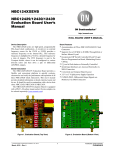
Stellaris® LM3S6965
Evaluation Board
U S E R ’S M A N U A L
EK-LM3S696 5-05
Co pyrigh t © 200 7-200 8 Lumin ary Micro, In c.
Legal Disclaimers and Trademark Information
INFORMATION IN THIS DOCUMENT IS PROVIDED IN CONNECTION WITH LUMINARY MICRO PRODUCTS. NO LICENSE,
EXPRESS OR IMPLIED, BY ESTOPPEL OR OTHERWISE, TO ANY INTELLECTUAL PROPERTY RIGHTS IS GRANTED BY THIS
DOCUMENT. EXCEPT AS PROVIDED IN LUMINARY MICRO’S TERMS AND CONDITIONS OF SALE FOR SUCH PRODUCTS,
LUMINARY MICRO ASSUMES NO LIABILITY WHATSOEVER, AND LUMINARY MICRO DISCLAIMS ANY EXPRESS OR IMPLIED
WARRANTY, RELATING TO SALE AND/OR USE OF LUMINARY MICRO’S PRODUCTS INCLUDING LIABILITY OR WARRANTIES
RELATING TO FITNESS FOR A PARTICULAR PURPOSE, MERCHANTABILITY, OR INFRINGEMENT OF ANY PATENT, COPYRIGHT
OR OTHER INTELLECTUAL PROPERTY RIGHT. LUMINARY MICRO’S PRODUCTS ARE NOT INTENDED FOR USE IN MEDICAL,
LIFE SAVING, OR LIFE-SUSTAINING APPLICATIONS.
Luminary Micro may make changes to specifications and product descriptions at any time, without notice. Contact your local Luminary Micro
sales office or your distributor to obtain the latest specifications before placing your product order.
Designers must not rely on the absence or characteristics of any features or instructions marked "reserved" or "undefined." Luminary Micro
reserves these for future definition and shall have no responsibility whatsoever for conflicts or incompatibilities arising from future changes to
them.
Copyright © 2007–2008 Luminary Micro, Inc. All rights reserved. Stellaris, Luminary Micro, and the Luminary Micro logo are registered
trademarks of Luminary Micro, Inc. or its subsidiaries in the United States and other countries. ARM and Thumb are registered trademarks, and
Cortex is a trademark of ARM Limited. Other names and brands may be claimed as the property of others.
Luminary Micro, Inc.
108 Wild Basin, Suite 350
Austin, TX 78746
Main: +1-512-279-8800
Fax: +1-512-279-8879
http://www.luminarymicro.com
2
October 28, 2008
Stellaris® LM3S6965 Evaluation Board
Table of Contents
Chapter 1: Stellaris® LM3S6965 Evaluation Board ....................................................................................... 7
Features.............................................................................................................................................................. 8
Block Diagram .................................................................................................................................................... 8
Evaluation Kit Contents ...................................................................................................................................... 9
Evaluation Board Specifications ..................................................................................................................... 9
Features of the LM3S6965 Microcontroller......................................................................................................... 9
Chapter 2: Hardware Description .................................................................................................................. 11
LM3S6965 Microcontroller ................................................................................................................................ 11
Device Overview ........................................................................................................................................... 11
Ethernet ........................................................................................................................................................ 11
Clocking ........................................................................................................................................................ 11
Reset............................................................................................................................................................. 11
Power Supplies ............................................................................................................................................. 12
Debugging..................................................................................................................................................... 12
USB Device Controller Functions ..................................................................................................................... 13
Device Overview ........................................................................................................................................... 13
USB to JTAG/SWD ....................................................................................................................................... 13
Virtual COM Port........................................................................................................................................... 13
Serial Wire Out.............................................................................................................................................. 13
Organic LED Display ........................................................................................................................................ 13
Features........................................................................................................................................................ 13
Control Interface ........................................................................................................................................... 14
Power Supply................................................................................................................................................ 14
Design Guidelines......................................................................................................................................... 14
Further Reference......................................................................................................................................... 14
Other Peripherals.............................................................................................................................................. 14
Speaker......................................................................................................................................................... 14
MicroSD Card Slot ........................................................................................................................................ 14
Push Switches .............................................................................................................................................. 14
User LED ...................................................................................................................................................... 15
Bypassing Peripherals ...................................................................................................................................... 15
Interfacing to the EVB....................................................................................................................................... 15
Using the In-Circuit Debugger Interface ........................................................................................................... 16
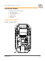
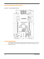
Appendix A: Schematics................................................................................................................................ 17
Appendix B: Connection Details ................................................................................................................... 23
Component Locations....................................................................................................................................... 23
Evaluation Board Dimensions........................................................................................................................... 24
I/O Breakout Pads ............................................................................................................................................ 24
Recommended Connectors .............................................................................................................................. 25
ARM Target Pinout ........................................................................................................................................... 26
References ....................................................................................................................................................... 26
Appendix C: Contact Information ................................................................................................................. 29
October 28, 2008
3
List of Figures
Figure 1-1.
Figure 1-2.
Figure 2-1.
Figure A-1.
Figure A-2.
Figure A-3.
Figure A-4.
Figure B-1.
Figure B-2.
4
Stellaris LM3S6965 Evaluation Board Layout ................................................................................. 7
LM3S6965 Evaluation Board Block Diagram .................................................................................. 8
ICD Interface Mode ....................................................................................................................... 16
LM3S6965 Microcontroller (sheet 1 of 3) ...................................................................................... 18
LM3S6965 Microcontroller (sheet 2 of 3) ...................................................................................... 19
LM3S6965 Microcontroller (sheet 3 of 3) ...................................................................................... 20
PLD schematic .............................................................................................................................. 21
Component Locations ................................................................................................................... 23
Evaluation Board Dimensions ....................................................................................................... 24
October 28, 2008
Stellaris® LM3S6965 Evaluation Board
List of Tables
Table 2-1.
Table 2-2.
Table B-1.
Table B-2.
Table B-3.
Stellaris LM3S6965 Evaluation Board Hardware Debugging Configurations................................ 12
Isolating On-Board Hardware........................................................................................................ 15
I/O Breakout Pads ......................................................................................................................... 25
Recommended Connectors........................................................................................................... 25
20-Pin JTAG/SWD Configuration .................................................................................................. 26
October 28, 2008
5
6
October 28, 2008
C H A P T E R 1
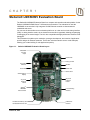
Stellaris® LM3S6965 Evaluation Board
The Stellaris® LM3S6965 Evaluation Board is a compact and versatile evaluation platform for the
Stellaris LM3S6965 ARM® Cortex™-M3-based microcontroller. The evaluation kit uses the
LM3S6965 microcontroller’s fully integrated 10/100 Ethernet controller to demonstrate an
embedded web server.
You can use the board either as an evaluation platform or as a low-cost in-circuit debug interface
(ICDI). In debug interface mode, the on-board microcontroller is bypassed, allowing programming
or debugging of an external target. The kit is also compatible with high-performance external JTAG
debuggers.
This evaluation kit enables quick evaluation, prototype development, and creation of applicationspecific designs for Ethernet networks. The kit also includes extensive source-code examples,
allowing you to start building C code applications quickly.
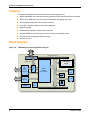
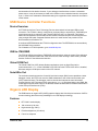
Figure 1-1.
Stellaris LM3S6965 Evaluation Board Layout
-7$*6:'
LQSXWDQG
RXWSXW
1DYLJDWLRQ
6ZLWFKHV
3RZHU/('
2/('*UDSKLFV
'LVSOD\
SLQ,2
EUHDNRXW
KHDGHU
6WHOODULV70
/06
0LFURFRQWUROOHU
PLFUR6'&DUG0HPRU\6ORW
EDVH7(WKHUQHW-DFN
October 28, 2008
P
h
e
c
a
l
m
I
r
e
d
l
o
e
g
a
5HVHWVZLWFK
'HEXJRXW/('
6SHDNHU
6WDWXV/('
6HOHFWVZLWFK
SLQ,2
EUHDNRXW
KHDGHU
,QFLUFXLW'HEXJ
,QWHUIDFH
86%'HYLFH
,QWHUIDFH
7
Stellaris® LM3S6965 Evaluation Board
Features
The Stellaris LM3S6965 Evaluation Board includes the following features:
Stellaris LM3S6965 microcontroller with fully-integrated 10/100 embedded Ethernet controller
Simple setup; USB cable provides serial communication, debugging, and power
OLED graphics display with 128 x 96 pixel resolution
User LED, navigation switches, and select pushbuttons
Magnetic speaker
LM3S6965 I/O available on labeled break-out pads
Standard ARM® 20-pin JTAG debug connector with input and output modes
USB interface for debugging and power supply
MicroSD card slot
Block Diagram
LM3S6965 Evaluation Board Block Diagram
Target
Cable
Figure 1-2.
Dual
USB
Device
Controller
UART0
OLED Display
128 x 96
Stellaris
LM3S6965
Microcontroller
I/O Signals
USB Cable
USB
SWD/JTAG
Mux
JTAG/SWD
Output/Input
Debug
I/O Signal Break-out
Switch
LED
CAT5 Cable
USB
RJ45
Jack+
Magnetics
+3.3V
Regulator
Nav
Switch
Speaker
Reset
I/O Signal Break-out
8
October 28, 2008
Stellaris® LM3S6965 Evaluation Board
Evaluation Kit Contents
The evaluation kit contains everything needed to develop and run applications for Stellaris
microcontrollers including:
LM3S6965 Evaluation Board (EVB)
USB cable
20-pin JTAG/SWD target cable
CD containing:
– A supported, evaluation version of one of the following:
•
Keil™ RealView® Microcontroller Development Kit (MDK-ARM)
•
IAR Embedded Workbench® development tools
•
Code Sourcery GCC development tools
•
Code Red Technologies development tools
– Complete documentation
– Quickstart guide
– Quickstart source code
– Stellaris® Firmware Development Package with example source code
Evaluation Board Specifications
Board supply voltage:
4.37–5.25 Vdc from USB connector
Board supply current:
250 mA typ (fully active, CPU at 50 MHz)
Break-out power output:
3.3 Vdc (60 mA max), 15 Vdc (15 mA max)
Dimensions:
4.0” x 2.45” x 0.7” (LxWxH)
RoHS status:
Compliant
Features of the LM3S6965 Microcontroller
32-bit RISC performance using ARM® Cortex™-M3 v7M architecture
– 50-MHz operation
– Hardware-division and single-cycle-multiplication
– Integrated Nested Vectored Interrupt Controller (NVIC)
– 42 interrupt channels with eight priority levels
256 KB single-cycle Flash
64 KB single-cycle SRAM
Four general-purpose 32-bit timers
Integrated Ethernet MAC and PHY
Three fully programmable 16C550-type UARTs
Four 10-bit channels (inputs) when used as single-ended inputs
Two independent integrated analog comparators
October 28, 2008
9
Stellaris® LM3S6965 Evaluation Board
Two I2C modules
Three PWM generator blocks
– One 16-bit counter
– Two comparators
– Produces two independent PWM signals
– One dead-band generator
10
Two QEI modules with position integrator for tracking encoder position
0 to 42 GPIOs, depending on user configuration
On-chip low drop-out (LDO) voltage regulator
October 28, 2008
C H A P T E R 2
Hardware Description
In addition to a microcontroller, the Stellaris LM3S6965 evaluation board includes a range of useful
peripherals and an integrated ICDI. This chapter describes how these peripherals operate and
interface to the MCU.
LM3S6965 Microcontroller
Device Overview
The heart of the EVB is a Stellaris LM3S6965 ARM Cortex-M3-based microcontroller. The
LM3S6965 offers 256 KB Flash memory, 50-MHz operation, an Ethernet controller, and a wide
range of peripherals. Refer to the LM3S6965 data sheet (order number DS-LM3S6965) for
complete device details.
The LM3S6965 microcontroller is factory programmed with a quickstart demo program. The
quickstart program resides in the LM3S6965 on-chip Flash memory and runs each time power is
applied, unless the quickstart has been replaced with a user program.
Ethernet
A key feature of the LM3S6965 microcontroller is its fully integrated Ethernet controller. Only a
RJ45 jack with integrated magnetics and a few passive components are needed to complete the
10/100baseT interface. The RJ45 jack incorporates LEDs that indicate traffic and link status.
These are automatically managed by on-chip microcontroller hardware. Alternatively, the LEDs
can be software controlled by configuring those pins as general-purpose outputs.
The LM3S6965 supports automatic MDI/MDI-X so the EVB can connect directly to a network or to
another Ethernet device without requiring a cross-over cable.
Clocking
The LM3S6965 microcontroller has four on-chip oscillators, three are implemented on the EVB. A
8.0-MHz crystal completes the LM3S6965’s main internal clock circuit. An internal PLL, configured
in software, multiples this clock to 50-MHz for core and peripheral timing.
A small, 25-MHz crystal is used by the LM3S6965 microcontroller for Ethernet physical layer
timing and is independent of the main oscillator.
Reset
The LM3S6965 microcontroller shares its external reset input with the OLED display. In the EVB,
reset sources are gated through the CPLD, though in a typical application a simple wired-OR
arrangement is sufficient.
Reset is asserted (active low) under any one of three conditions:
Power-on reset
Reset push switch SW1 held down
Internal debug mode—By the USB device controller (U4 FT2232) when instructed by
debugger
October 28, 2008
11
Hardware Description
Power Supplies
The LM3S6965 is powered from a +3.3-V supply. A low drop-out (LDO) regulator regulates +5-V
power from the USB cable to +3.3-V. +3.3-V power is available for powering external circuits.
A +15-V rail is available when the OLED display is active. The speaker and OLED display
boost-converter operate directly from the +5-V rail.
Debugging
Stellaris microcontrollers support programming and debugging using either JTAG or SWD. JTAG
uses the signals TCK, TMS, TDI, and TDO. SWD requires fewer signals (SWCLK, SWDIO, and,
optionally, SWO, for trace). The debugger determines which debug protocol is used.
Debugging Modes
The LM3S6965 evaluation board supports a range of hardware debugging configurations.
Table 2-1 summarizes these configurations.
Table 2-1. Stellaris LM3S6965 Evaluation Board Hardware Debugging Configurations
Mode
Debug Function
Use
Selected by
1
Internal ICDI
Debug on-board LM3S6965
microcontroller over USB
interface.
Default mode
2
ICDI out to JTAG/SWD
header
The EVB is used as a USB to
SWD/JTAG interface to an
external target.
Connecting to an external
target and starting debug
software. The red Debug Out
LED will be ON.
3
In from JTAG/SWD header
For users who prefer an
external debug interface
(ULINK, JLINK, etc.) with the
EVB.
Connecting an external
debugger to the JTAG/SWD
header.
Modes 2 and 3 automatically detect the presence of an external debug cable. When the debugger
software is connected to the EVB's USB controller, the EVB automatically selects Mode 2 and
illuminates the red Debug Out LED.
Debug In Considerations
Debug Mode 3 supports evaluation board debugging using an external debug interface. Mode 3 is
automatically selected when a device such as a Segger J-Link or Keil ULINK is connected.
Boards marked Revision D or later automatically configure pin 1 to be a 3.3-V reference, if an
external debugger is connected. To determine the revision of your board, locate the product
number on the bottom of the board; for example, EK-LM3S6965-D. The last character of the
product number identifies the board revision.
A configuration or board-level change may be necessary when using an external debug interface
with revisions A through C of this evaluation board. Because the evaluation board supports both
debug out and debug in modes, pin 1 of the 20-pin JTAG/SWD header is, by default, not
connected to +3.3 V. Consequently, devices requiring a voltage on pin 1 to power their line buffers
may not work.
Two solutions exist. Some debugger interfaces (such as ULINK) have an internal power jumper
that, in this case, should be set to internal +3.3-V power. Refer to debugger interface
12
October 28, 2008
Stellaris® LM3S6965 Evaluation Board
documentation for full details. However, if your debugger interface does not have a selectable
power source, it may be necessary to install a 0-Ω resistor on the evaluation board to route power
to pin 1. Refer to the schematics and board drawing in the appendix of this manual for the location
of this resistor.
USB Device Controller Functions
Device Overview
An FT2232 device from Future Technology Devices International Ltd manages USB-to-serial
conversion. The FT2232 is factory configured by Luminary Micro to implement a JTAG/SWD port
(synchronous serial) on channel A and a Virtual COM Port (VCP) on channel B. This feature
allows two simultaneous communications links between the host computer and the target device
using a single USB cable. Separate Windows drivers for each function are provided on the
Documentation and Software CD.
A small serial EEPROM holds the FT2232 configuration data. The EEPROM is not accessible by
the LM3S6965 microcontroller.
For full details on FT2232 operation, go to www.ftdichip.com.
USB to JTAG/SWD
The FT2232 USB device performs JTAG/SWD serial operations under the control of the debugger.
A CPLD (U2) multiplexes SWD and JTAG functions and, when working in SWD mode, provides
direction control for the bidirectional data line.
Virtual COM Port
The Virtual COM Port (VCP) allows Windows applications (such as HyperTerminal) to
communicate with UART0 on the LM3S6965 over USB. Once the FT2232 VCP driver is installed,
Windows assigns a COM port number to the VCP channel.
Serial Wire Out
The evaluation board supports the Cortex-M3 serial-wire output (SWO) trace capabilities. Under
debugger control, the CPLD can route the SWO datastream to the virtual communication port
(VCP) transmit channel. The debugger can then decode and interpret the trace information
received from the VCP. The normal VCP connection to UART0 is interrupted when using SWO. Not
all debuggers support SWO. Refer to the Stellaris LM3S3748 data sheet for additional information
on the trace port interface unit (TPIU).
Organic LED Display
The EVB features an organic LED (OLED) graphics display with 128 x 96 pixel resolution. OLED is
a new technology that offers many advantages over LCD display technology.
Features
RiT P14201 series display
128 columns by 96 rows
High-contrast (typ. 500:1)
Excellent brightness (120 cd/m2)
Fast 10 us response
October 28, 2008
13
Hardware Description
Control Interface
The OLED display has a built-in controller IC with synchronous serial and parallel interfaces.
Synchronous serial (SSI) is used on the EVB as it requires fewer microcontroller pins. Data cannot
be read from the OLED controller; only one data line is necessary. Note that the SSI port is shared
with the microSD card slot. The Stellaris® Firmware Development Package (included on the
Documentation and Software CD) contains complete drivers with source-code for the OLED
display.
Power Supply
A +15-V supply is needed to bias the OLED display. A FAN5331 device from Fairchild combines
with a few external components to complete a boost converter. When the OLED display is
operating, a small amount of power can be drawn from the +15-V rail to power other devices.
Design Guidelines
The OLED display has a lifetime of about 13,000 hours. It is also prone to degradation due to
burn-in, similar to CRT and plasma displays. The quickstart application includes both a screen
saver and a power-down mode to extend display life. These factors should be considered when
developing EVB applications that use the OLED display.
When using the EVB as an in-circuit debug interface (ICDI), the OLED display is held in reset to
reduce power consumption and eliminate display wear-out.
Further Reference
For additional information on the RiT OLED display, visit www.ritekdisplay.com.
Other Peripherals
Speaker
A small, magnetic audio transducer connects through a MOSFET to PD1/PWM1, allowing a range
of options for generating simple and complex tones. Use of the +5-V rail reduces switching noise
on the +3.3-V rail.
MicroSD Card Slot
Removable Flash cards are an ideal media for storing data such as web page content. The source
code on the CD includes example code for reading data from standard FAT formatted SD cards.
All data and control transactions use the SD card’s SPI mode. Note that the SD card specification
does not require that a card supports the SPI mode, but most cards do so in practice. Cards from
several vendors have been used with the EVB.
MicroSD cards are very small and require careful handling. the SD card slot on the EVB is a pushpush type (push to insert; push again to eject).
Note: To avoid damage, remove power before inserting or removing cards.The EVB does not
implement SD card power control.
Push Switches
The EVB has five general-purpose input switches. Four are arranged in a navigation-style
configuration. The fifth functions as a Select switch.
14
October 28, 2008
Stellaris® LM3S6965 Evaluation Board
User LED
A user LED (LED3) is provided for general use. The LED is connected to PC5/CCP1, allowing the
option of either GPIO or PWM control (brightness control). Refer to the Quickstart Application
source code for an example of PWM control.
Bypassing Peripherals
Excluding Ethernet, the EVB’s on-board peripheral circuits require 16 GPIO lines. Two additional
GPIO lines are assigned to Ethernet LEDs. This leaves 20 GPIO lines and 4 ADC channels
immediately available for connection to external circuits. If an application requires more GPIO
lines, the on-board hardware can be disconnected. The EVB is populated with 16 jumper links,
which can be cut with a knife to isolate on-board hardware. The process can be reversed by
installing 0603- 0-ohm chip resistors.
Important: The quickstart application will not run if one or more jumpers are removed.
Table 2-2. Isolating On-Board Hardware
MCU Pin
EVB Function
To Isolate, Remove...
Pin 26 PA0/U0RX
Virtual COM port receive
JP1
Pin 27 PA1/U0TX
Virtual COM port transmit
JP2
Pin 10 PD0/IDX0
SD card chip select
JP3
Pin 11 PD1/PWM1
Sound
JP4
Pin 30 PA4/SSI0RX
SD card data out
JP5
Pin 31 PA5/SSI0TX
SD card and OLED display data in
JP6
Pin 28 PA2/SSI0CLK
SD card and OLED display clock
JP7
Pin 22 PC7/PHB0
OLED display data/control select
JP8
Pin 29 PA3/SSI0FSS
OLED display chip select
JP9
Pin 73 PE1/PWM5
Down switch
JP10
Pin 74 PE2/PHB1
Left switch
JP11
Pin 72 PE0/PWM4
Up switch
JP12
Pin 75 PE3/PHA1
Right switch
JP13
Pin 61 PF1/IDX1
Select switch
JP14
Pin 47 PF0/PWM0
User LED
JP15
Pin 23 PC6/CCP3
Enable +15 V
JP16
Interfacing to the EVB
An array of accessible I/O signals makes it easy to interface the EVB to external circuits. All
LM3S6965 I/O lines (except those with both JTAG and SWD functions) are brought out to 0.1”
pitch pads. For quick reference, silk-screened labels on the PCB show primary pin functions.
Table B-1 on page 25 has a complete list of I/O signals as well as recommended connectors.
October 28, 2008
15
Hardware Description
Most LM3S6965 I/O signals are +5-V tolerant. Refer to the LM3S6965 data sheet for detailed
electrical specifications.
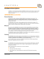
Using the In-Circuit Debugger Interface
The Stellaris LM3S6965 Evaluation Kit can operate as an In-Circuit Debugger Interface (ICDI).
ICDI acts as a USB to the JTAG/SWD adaptor, allowing debugging of any external target board
that uses a Stellaris microcontroller. See “Debugging Modes” on page 12 for a description of how
to enter Debug Out mode.
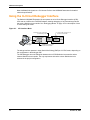
Figure 2-1.
ICD Interface Mode
Connecting Pin 18 to GND sets
external debug mode
Evaluation Board
USB
`
PC with IDE/
debugger
Stellaris
MCU
JTAG or SWD connects to the
external microcontroller
Target
Cable
Stellaris
MCU
Target
Board
TCK/SWCLK bypasses the
on- board microcontroller
The debug interface operates in either Serial-Wire Debug (SWD) or full JTAG mode, depending on
the configuration in the debugger IDE.
The IDE/debugger does not distinguish between the on-EVB Stellaris microcontroller and an
external Stellaris microcontroller. The only requirement is that the correct Stellaris device is
selected in the project configuration.
16
October 28, 2008
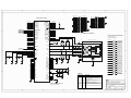
A P P E N D I X A
Schematics
Schematics for the Stellaris LM3S6965 Evaluation Board follow.
October 28, 2008
17
2
3
4
PD4/CCP0
34
PD6/FAULT
Stellaris Microcontroller
A
INT_TCK
TMS/SWDIO
PC2/TDI
PC3/TDO
B
26
27
28
29
30
31
34
35
TMS/SWDIO
PC2/TDI
PC3/TDO
PC4/PhA0
PC5/C1+/C0o
PC6/CCP3
PC7/PhB0
80
79
78
77
25
24
23
22
PE0/PWM4
PE1/PWM5
PE2/PhB1
PE3/PhA1
72
73
74
75
ADC0
ADC1
ADC2
ADC3
1
2
5
6
19
18
PG0/U2RX
PG1/U2TX
64
MCURSTn
17
16
48
49
1
Y1
2
1
25.00MHz
OSC32IN
OSC32OUT
2
52
53
8.00MHz
C8
C
Y3
C9
18PF
18PF
C40
18PF
50
51
65
76
C41
18PF
9
15
21
33
39
42
45
54
57
63
69
82
85
86
87
94
4
97
PA0/U0RX
PA1/U0TX
PA2/SSI0CLK
PA3/SSI0FSS
PA4/SSI0RX
PA5/SSI0TX
PA6/I2C1SCL
PA7/I2C1SDA
PC0/TCK/SWCLK
PC1/TMS/SWDIO
PC2/TDI
PC3/TDO/SWO
PC4/PhA0
PC5/C1+/C0o
PC6/CCP3
PC7/PhB0
PE0/PWM4
PE1/PWM5
PE2/PhB1
PE3/PhA1
ADC0
ADC1
ADC2
ADC3
PB0/PWM2
PB1/PWM3
PB2/I2C0SCL
PB3/I2C0SDA
PB4/C0PB5/C1PB6/C0+
PB7/TRST
PD0/IDX0
PD1/PWM1
PD2/U1RX
PD3/U1TX
PD4/CCP0
PD5/CCP2
PD6/FAULT
PD7/CCP1
PF0/PWM0
PF1/IDX1
PF2/LED1
PF3/LED0
MDIO
TXOP
66
67
70
71
92
91
90
89
PB0/PWM2
PB1/PWM3
PB2/I2C0SCL
PB3/I2CSDA
PB4/C0PB5/C1PB6/C0+
10
11
12
13
95
96
99
100
PD0/IDX0
PD1/PWM1
PD2/U1RX
PD3/U1TX
PD4/CCP0
PD5/CCP2
PD6/FAULT
PD7/CCP1
47
61
60
59
PF0/PWM0
PF1/IDX1
PF2/LED1
PF3/LED0
+3.3V
R33
10K
XTALNPHY
XTALPPHY
PB4/C0PD5/CCP2
PD7/CCP1
ADC0
ADC2
PD1/PWM1
PD3/U1TX
PG0/U2RX
PC6/CCP3
PC4/PhA0
PA0/U0Rx
PA2/SSI0CLK
PA4/SSI0RX
PA6/I2CSCL
+3.3V
PA1/U0Tx
PA3/SSI0FSS
PA5/SSI0TX
PA7/I2CSDA
PB7/TRST
2
1
+15V
PB5/C1PB7/TRST
PC3/TDO
PE2/PhB1
PE0/PWM4
PB2/I2C0SCL
PB1/PWM3
PF1/IDX1
PF3/LED0
RXIP
35
36
PB6/C0+
PC2/TDI
PE3/PhA1
A
PE1/PWM5
PB3/I2CSDA
PB0/PWM2
PF2/LED1
OSC32OUT
OSC32IN
59
PF0/PWM0
60
+3.3V
+5V
On-board Peripheral Signals
Jumpers can be cut to
free GPIO lines as required.
+3.3V
Ethernet 10/100baseT
JP1
P4
R1
58
+3.3V
R2
49.9
10K
R3
49.9
C1
10pF
R4
C2
10pF
C3
PA1/U0Tx
G-
3
PA2/SSI0CLK
1CT:1
+3.3V
0.1UF
46
PA3/SSI0FSS
RX+ 3
PA4/SSI0RX
JP6
RX- 6
+3.3V
PA5/SSI0TX
7
6
RXIN
XOSC0
XOSC1
WAKE
HIB
CMOD0
CMOD1
GND
GND
GND
GND
GND
GND
GND
GND
GND
GND
GND
GND
GND
GND
GND
GND
AGND
AGND
AVDD
AVDD
VDD33
VDD33
VDD33
VDD33
VDD33
VDD33
VDD33
VDD33
VDD33
VDD33
VDD33
VBAT
LDO
VDD25
VDD25
VDD25
VDD25
ERBIAS
D
0.1UF
37
+3.3V +3.3V
3
98
8
20
32
36
44
56
68
81
83
84
93
R6
49.9
C12
0.1UF
R7
49.9
C5
10pF
R5
C6
10pF
330
2
1
Y-
9
10
NC
Y+
PE0/PWM4
GND
UP_SWn
JP10
C7
0.01UF
PE1/PWM5
DOWN_SWn
C
JP11
PE2/PhB1
LEFT_SWn
JP13
PE3/PhA1
RIGHT_SWn
JP4
PD1/PWM1
+3.3V
SOUND
JP3
PD0/IDX0
C13
C14
C15
0.01UF 0.01UF 0.1UF
C16
0.1UF
CARDCSn
JP8
C17
4.7UF
PC7/PhB0
OLEDDC
JP16
7
C18
C19
0.01UF 0.1UF
14
38
62
88
PC6/CCP3
History
C20
4.7UF
Revision
Date
Description
A
5/12/07
First Production Release
B
6/29/07
Improve SWD out feature, add SWO support, 1-bit
OLED display option.
C
8/09/07
Change to RiT 128x96 OLED display
1/25/08
Install R27
3/25/08
Add R35 for future compatibility.
Tie R6/R7 to +3.3V. Add TVCC control.
R35
12.4K
D
12.4K 1% resistor required on Pin 41 for
compatibility with future LM3S6965 revisions.
See Product Change Notification.
D
Ethernet Evaluation Board
Page Title:
LM3S6965 Micro and 10/100 Ethernet
Date:
3
4
EN+15V
Drawing Title:
Size
2
SELECT_SWn
JP12
LM3S6965
1
LED
JP14
PF1/IDX1
J3011G21DNL
55
41
SSITX
JP15
PF0/PWM0
8
+3.3V
SSIRX
5
1CT:1
8
MOSCin
MOSCout
OLEDCSn
JP5
4
7
SSICLK
JP9
TX+ 1
TX- 2
4
40
C4
VCP_TX
JP7
330
43
VCP_RX
JP2
G+
12
11
B
PA0/U0Rx
+3.3V
5
TXON
6
I/O Break-out Headers
PG0/U2RX
PG1/U2TX
RST
33
ADC1
ADC3
PD0/IDX0
PD2/U1RX
PG1/U2TX
PC7/PhB0
PC5/C1+/C0o
U1
PA0/U0Rx
PA1/U0Tx
PA2/SSI0CLK
PA3/SSI0FSS
PA4/SSI0RX
PA5/SSI0TX
PA6/I2CSCL
PA7/I2CSDA
5
GL
GR
1
5
B
Document Number:
3/26/2008
1
Sheet
6
1
of
3
Rev
D
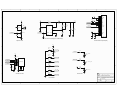
1
2
3
4
5
6
U2
1
2
3
4
5
6
7
8
9
10
11
12
13
14
15
16
17
18
19
20
21
22
23
24
25
C26
A
4.7UF
+3.3V
+5V
+5V
D2
L1
NR4018T100M
10uH
R9
2.2
+15V
U7
BZ1
5
1
2
D1
MBR0520
VIN
SW
C24
4.7UF
FB
NFT-03A
R13
200K
1
200K
OLEDCSn
MCURSTn
OLEDDC
MBR0520
R14
C27
120pF
SSICLK
SSITX
C22
3
C25
4.7UF
0.1UF
+3.3V
Q1
NDS331N
SOUND
4
EN+15V
R10
10K
R12
10K
SHDNn
GND
R11
17.8K
2
+15V
FAN5331
C23
0.1UF
C21
0.1UF
NC
VCIR
VCOMH
LVSS
VSS
BS1
BS2
IREF
CSn
RESn
D/Cn
R/Wn
E
D0/SCLK
D1/SDIN
D2
D3
D4
D5
D6
D7
VDDIO
VDD
VCC
NC
A
OLED-RIT-128X96
RGS13128096WH000
B
+15V 50mA Power Supply for OLED Display
Speaker Circuit
B
128x96 OLED Graphics Display
+3.3V
Reset
R15
10K
SW1
RESET_SWn
SW-B3S1000
R16
LED
330
C30
OMIT
LED2
Green
+3.3V
Select
C
R17
10K
+3.3V
SSICLK
SSIRX
+3.3V
SW-B3S1000
C
SELECT_SWn
Up
R18
DBGOUTLED
330
SW3
2908-05WB-MG
SW-B3S1000
UP_SWn
LED3
Red
Debug Out
LED4
Green
Power
Down
SW-B3S1000
12
11
9
SW4
R19
10K
10
C28
0.1UF
P3
1
2
3
4
5
6
7
8
CARDCSn
SSITX
Status
SW2
DOWN_SWn
+3.3V
Left
R20
330
SW5
+3.3V
SW-B3S1000
LEFT_SWn
Right
microSD Card Slot
SW6
D
SW-B3S1000
Status LEDs
D
RIGHT_SWn
User Switches
Drawing Title:
Ethernet Evaluation Board
Page Title:
OLED Display, Switches and Audio
Size
Date:
1
2
3
4
5
B
Document Number:
3/26/2008
2
Sheet
6
2
of
3
Rev
D
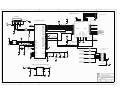
1
2
3
4
5
6
Debug Interface Logic
USB Interface
+3.3V
54819-0519
P1
6
ADBUS0
ADBUS1
ADBUS2
ADBUS3
ADBUS4
ADBUS5
ADBUS6
ADBUS7
3V3OUT
0.1UF
R21 27
8
R22 27
7
C32
USBDM
USBDP
0.01UF
ACBUS0
ACBUS1
ACBUS2
ACBUS3
SI/WUA
R23
1.5K
BDBUS0
BDBUS1
BDBUS2
BDBUS3
BDBUS4
BDBUS5
BDBUS6
BDBUS7
B
+5V
R24
10K
U5
VCC
NC
ORG
GND
CS
SK
DI
DO
1
2
3
4
48
1
2
47
R25
1.5K
CAT93C46
43
44
1K 64X16
1
Y2
2
4
5
+5V
6.00MHz
C10
C11
18PF
18PF
EECS
EESK
EEDATA
TEST
BCBUS0
BCBUS1
BCBUS2
BCBUS3
SI/WUB
XTIN
XTOUT
RESET#
RSTOUT#
PWREN#
44
45
46
47
48
2
3
4
7
8
9
10
14
INT_TCK
TCK
TDI/DI
TDO/DO
TMS/OUTEN
24
23
22
21
20
19
17
16
SRSTN
DBG_JTAG_EN
15
13
12
11
10
RESET_SWn
+3.3V
+3.3V
40
39
38
37
36
35
33
32
VCP_RX
TP4
+3.3V
45
C
GND
GND
GND
GND
VCC
VCC
VCCIOA
VCCIOB
AGND
AVCC
PLD JTAG TEST POINTS
TP5
TP6
12
36
VCC
VCC
11
25
1
35
TCK
TMS
TDI
TDO
U3
LC4032V-75TN48C
Bank 1
20
21
22
23
24
26
27
28
31
32
33
34
38
B0
B1
B2
B3
B4
B5
B6
B7
B8
B9
B10
B11
B12
PC2/TDI
PC3/TDO
TARGETCABLEn
DBGOUTLED
VCP_TX
PB7/TRST
MCURSTn
B
R34
4.7K
+3.3V
TMS/SWDIO
TCK/SWCLK
SWO_EN
C42
0.1UF
30
29
28
27
26
MODE is reserved
for future use.
MODE
VCP_TX_SWO
+3.3V
R27
41
JTAG/SWD Interface
Input/Output
27
PC2/TDI
+5V
9
18
25
34
A0/GOE0
A1
A2
A3
A4
A5
Bank 0
A6
A7
A8
A9
A10
A11
A12
B15/GOE1
B14
B13
C31
60ohm @ 100 MHz
8
7
6
5
TP3
PLD_TDO
41
40
39
5
4
3
2
1
R8
4.7K
U4
VCCO (Bank 1)
GND (Bank 1)
USB Device Controller
Omit
+5V
C29
0.1UF
30
29
+3.3V
18
43
19
42
7 USBSH
CLK1/I
CLK0/I
CLK2/I
CLK3/I
6
FB1
TP2
PLD_TDI
A
JP17
GND (Bank 0)
VCCO (Bank 0)
G
5
6
ID
13
37
D+
GND
GND
D-
A13
A14
A15
5V
USB+5V
TP1
PLD_TMS
+3.3V
15
16
17
A
PLD_TCK
3
42
14
31
R26
PC2/TDI
27
P2
+3.3v
TMS/SWDIO
R30
46
C37
330
C33
C34
C35
C36
0.1UF
0.1UF
0.1UF
0.1UF
TCK/SWCLK
FT2232D
TMS/SWDIO
TCK/SWCLK
R28
XVCC
27
XTDI
XTMS
XTCK
R29
XTDO
1
3
5
7
9
11
13
15
17
19
27
0.1UF
Channel A : JTAG / SW Debug
Channel B : Virtual Com Port
PC3/TDO
R31
PC3/TDO
JP18
+5V
Header 10X2
6
VIN1
VOUT
VIN2
SENSE
C38
4.7UF
NC
2
D
GND
4.7K
GND
4
5
C39
4.7UF
3
7
D
LP8345ILD-3.3
Drawing Title:
Ethernet Evaluation Board
Page Title:
USB, Debugger Interfaces and Power
Size
Date:
1
2
+3.3v
R32
TARGETCABLEn
+3.3V
U6
1
C
27
USB +5V to +3.3V 500mA Power Supply
USB+5V
2
4
6
8
10
12
14
16
18
20
3
4
5
B
Document Number:
3/26/2008
3
Sheet
6
3
of
3
Rev
D
A
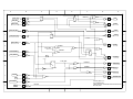
B
C
1
D
I90
SWO_EN
10
FTDI_TCK
45
DBGOUT
I105
44
I85
I86
ITCK
I109
41
I7
2
H
1
B
A
S
I91
G
S
A
B
34
F
FTDI_DBG
I89
VCP_TX
E
XTCK
2
I87
FTDI_TDI_DO
46
I6
I92
32
U0TX
24
XTDO
S
3
FTDI_TDO_DI
I3
B
A
47
I16
JTAGEN
I18
FTDI_TMS
48
I111
I4
21
4
JTAGEN
I20
FTDI_DBG
5
FTDIJTAGEN
4
FTDI_SRSTn
3
3
I35
S
SWDEN
I36
I5
I37
I2
XTDI
4
I112
B
A
I17
I9
40
XTMS
5
I8
D
FTDI_DBG
Q
DBGOUT
31
I96
6
C
7
I95
I99
33
I102
RSTSW
9
RC
14
EXTCABLEn
26
HIBn
16
7
8
A
DBGLED
6
INTDBG
I100
I42
I15
38
I104
I70
I106
I107
TEST
TRSTn
MCURSTn
7
I74
Luminary Micro, Inc.
Fury Evaluation Kit
JTAG Logic with Auto Mode Detect and Hibernate
AUG 23, 2007
I13
DRVEN
I108
B
C
D
E
F
G
H
8
22
October 28, 2008
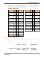
A P P E N D I X B
Connection Details
This appendix contains the following sections:
Component Locations
Evaluation Board Dimensions
I/O Breakout Pads
ARM Target Pinout
References
Component Locations
Figure B-1. Component Locations
October 28, 2008
23
Evaluation Board Dimensions
Figure B-2. Evaluation Board Dimensions
I/O Breakout Pads
The LM3S6965 EVB has 44 I/O pads, 14 power pads, and 2 crystal connections, for a total of 60
pads. Connection can be made by soldering wires directly to these pads, or by using 0.1” pitch
headers and sockets.
24
October 28, 2008
Stellaris® LM3S6965 Evaluation Board
Note: In Table B-2, an asterisk (*) by a signal name (also on the EVB PCB) indicates the signal is
normally used for on-board functions. Normally, you should cut the associated jumper (JP1-15)
before using an assigned signal for external interfacing.
Table B-1. I/O Breakout Pads
Pad
No.
Pad
No.
Pad
No.
Pad
No.
PD4/CCP0
34
33
PB4/C0-
+12 V
60
59
GND
PD6/FAULT
32
31
PD5/CCP2
PB5/C1-
58
57
PB6/C0+
GND
30
29
PD7/CCP1
PB7/TRST
56
55
PC2/TDI*
ADC1
28
27
ADC0
PC3/TDO*
54
53
PE3/PHA1*
ADC3
26
25
ADC2
PE2/PHB1
52
51
GND
IDX0*
24
23
GND
PE0/PWM4
50
49
PE1/PWM5*
PD2/U1RX
22
21
PD1/PWM1
PB2/SCL0
48
47
PB3/SDA0
PG2/U2TX
20
19
PD3/U1TTX
PB1/PWM3
46
45
GND
PC7/PHB0*
18
17
PG0/U2RX
PF1/IDX1
44
43
PB0/PWM2
PC5/C1+
16
15
PC6/CCP3*
PF3/LED0
42
41
PF2/LED1
GND
14
13
PC4/PHA0
GND
40
39
OSC32
+3.3 V
12
11
PA0/U0RX*
GND
38
37
OSC32
PA1/U0TX*
10
9
PA2/SSICLK*
PF0/PWM0
36
35
+3.3 V
PA3/SFSS*
8
7
PA4/SSIRX*
PA5/SSITX*
6
5
PA6/SCL1
PA7/SDA1
4
3
GND
GND
2
1
+5 V
Description
Description
Description
Description
Recommended Connectors
Connection can be made by soldering wires directly to pads or using 0.1” pitch headers and
sockets.
Table B-2. Recommended Connectors
Pins 1-34 (2 x 17 way)
Pins 35-06 (2 x 13 way)
October 28, 2008
PCB Socket
Sullins PPPC172LFBN-RC
Digikey S7120-ND
Cable Socket
3M 89134-0101
Digikey MKC34A-ND
Pin Header
Sullins PEC17DAAN
Digikey S2012E-17-ND
PCB Socket
Sullins PPPC132LFBN-RC
Digikey S7116-ND
Cable Socket
3M 89126-0101
Digikey MKC26A-ND
Pin Header
Sullins PEC13DAAN
Digikey S2012-13-ND
25
ARM Target Pinout
In ICDI input and output mode, the Stellaris LM3S6965 Evaluation Kit supports ARM’s standard
20-pin JTAG/SWD configuration. The same pin configuration can be used for debugging over
Serial Wire Debug (SWD) and JTAG interfaces. The debugger software, running on the PC,
determines which interface protocol is used.
The Stellaris target board should have a 2x10 0.1” pin header with signals as indicated in
Table B-3. This applies to both an external Stellaris MCU target (Debug output mode) and to
external JTAG/SWD debuggers (Debug input mode).
Table B-3. 20-Pin JTAG/SWD Configuration
Function
Pin
Pin
Function
VCC
1
2
nc
nc
3
4
GND
TDI
5
6
GND
TMS
7
8
GND
TCK
9
10
GND
NC
11
12
GND
TDO
13
14
GND
nc
15
16
GND
nc
17
18
GND
nc
19
20
GND
ICDI does not control RST (device reset) or TRST (test reset) signals. Both reset functions are
implemented as commands over JTAG/SWD, so these signals are not necessary.
It is recommended that connections be made to all GND pins; however, both targets and external
debug interfaces must connect pin 18 and at least one other GND pin to GND.
References
In addition to this document, the following references are included on the Stellaris Family
Development Kit documentation CD-ROM and are also available for download at
www.luminarymicro.com:
26
Stellaris LM3S6965 Evaluation Kit Quickstart Guide for appropriate tool kit (see “Evaluation Kit
Contents,” on page 9)
Stellaris LM3S6965 Read Me First for the ENET Evaluation Kit
Stellaris Family Peripheral Driver Library
Stellaris Family Peripheral Driver Library User’s Manual, publication PDL-LM3S6965
Stellaris LM3S6965 Data Sheet, publication DS-LM3S6965
October 28, 2008
Stellaris® LM3S6965 Evaluation Board
Additional references include:
Information on development tool being used:
– RealView MDK web site, www.keil.com/arm/rvmdkkit.asp
– IAR Embedded Workbench web site, www.iar.com
– Code Sourcery GCC development tools web site,
www.codesourcery.com/gnu_toolchains/arm
– Code Red Technologies development tools web site, www.code-red-tech.com
October 28, 2008
27
28
October 28, 2008
A P P E N D I X C
Contact Information
Company Information
Luminary Micro, Inc. designs, markets, and sells ARM Cortex-M3-based microcontrollers (MCUs).
Austin, Texas-based Luminary Micro is the lead partner for the Cortex-M3 processor, delivering the
world's first silicon implementation of the Cortex-M3 processor. Luminary Micro's introduction of
the Stellaris® family of products provides 32-bit performance for the same price as current 8- and
16-bit microcontroller designs. With entry-level pricing at $1.00 for an ARM technology-based
MCU, Luminary Micro's Stellaris product line allows for standardization that eliminates future
architectural upgrades or software tool changes.
Luminary Micro, Inc.
108 Wild Basin, Suite 350
Austin, TX 78746
Main: +1-512-279-8800
Fax: +1-512-279-8879
http://www.luminarymicro.com
Support Information
For support on Luminary Micro products, contact:
[email protected]
+1-512-279-8800, ext. 3
October 28, 2008
29
30
October 28, 2008