1
Chapter 4 Analog Device Reference
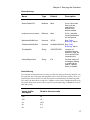
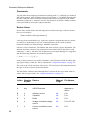
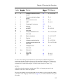
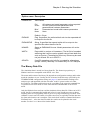
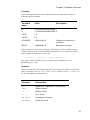
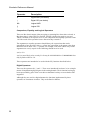
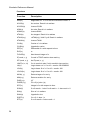
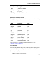
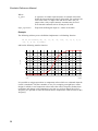
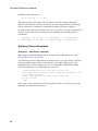
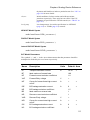
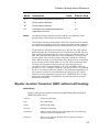
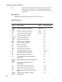
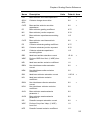
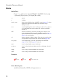
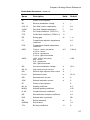
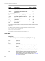
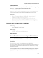
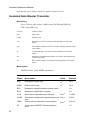
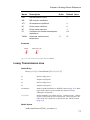
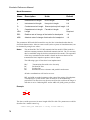
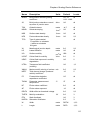
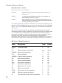
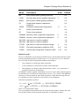
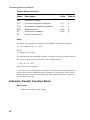
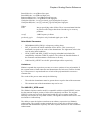
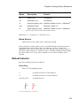
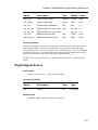
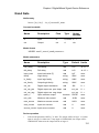
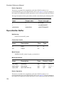
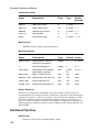
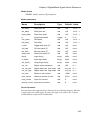
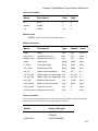
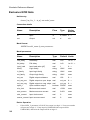
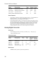
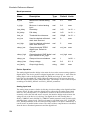
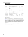
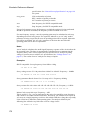
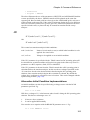
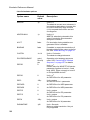
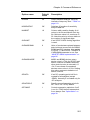
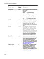
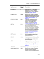
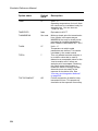
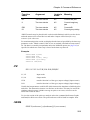
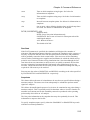
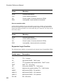
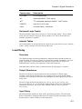
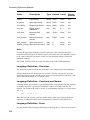
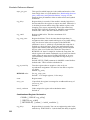
Diode Model Parameters - Level = 1
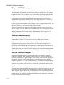
The symbols ' × ' and ' ÷ ' in the Area column means that that parameter should be
multiplied or divided by the area factor respectively.
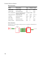
Name
Description
Units
Default Area
IS
Transport saturation current
A
1e-14
×
ISR
Recombination current parameter
A
0
×
N
Emission coefficient
1
NR
Emission Coefficient for ISR
2
IKF
High injection knee current
A
∞
×
RS
Series resistance
W
0
÷
TT
Transit time
sec
0
CJO or
CJ0
Zero bias junction capacitance
F
0
VJ
Junction potential
V
M
Grading coefficient
EG
Energy gap
XTI
Saturation current temperature
exponent
3
KF
Flicker noise coefficient
0
AF
Flicker noise exponent
1
FC
Forward bias depletion capacitance
coefficient
0.5
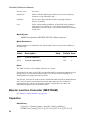
×
1
0.5
eV
1.11
BV
Reverse breakdown voltage
V
∞
IBV
Current at breakdown voltage
A
1e-10
TNOM
Parameter measurement
temperature
°C
27
TRS1
First order tempco RS
/°C
0
TRS2
Second order tempco RS
/°C2
0
TBV1
First order tempco BV
/°C
TBV2
Second order tempco BV
/°C2
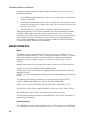
Notes
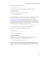
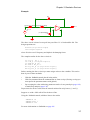
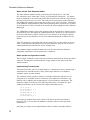
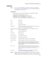
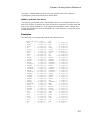
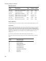
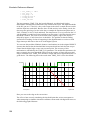
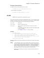
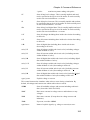
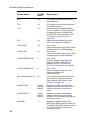
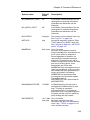
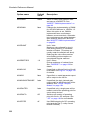
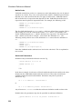
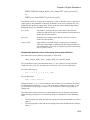
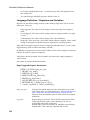
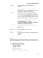
The dc characteristics of the diode are determined by the parameters IS, N,
ISR, NR and IKF. An ohmic resistance, RS, is included. Charge storage
effects are modelled by a transit time, TT, and a non-linear depletion layer
capacitance which is determined by the parameters CJO, VJ, and M. The
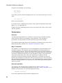
temperature dependence of the saturation current is defined by the
parameters EG, the energy and XTI, the saturation current temperature
×
65