1
Chapter 4 Analog Device Reference
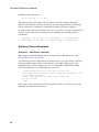
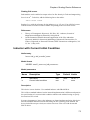
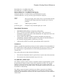
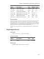
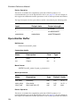
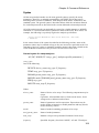
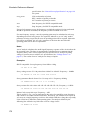
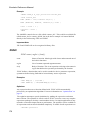
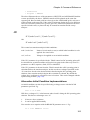
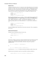
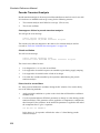
vds,vgs
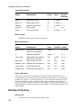
Initial conditions for drain-source and gate-source junctions
respectively. These only have an effect if the UIC parameter is
specified on the .TRAN control.
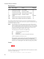
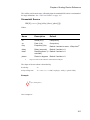
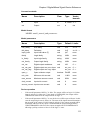
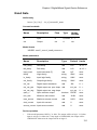
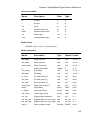
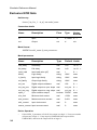
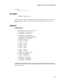
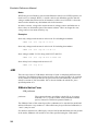
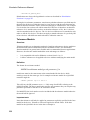
GaAsFET Model Syntax
.model modelname NMF ( parameters )
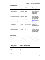
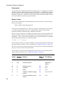
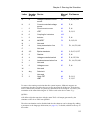
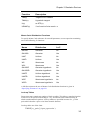
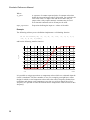
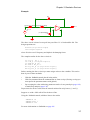
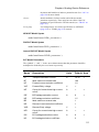
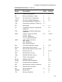
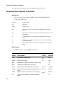
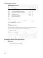
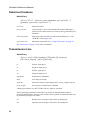
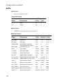
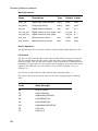
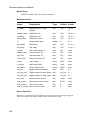
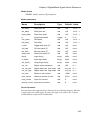
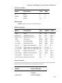
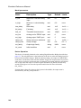
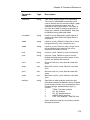
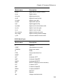
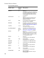
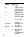
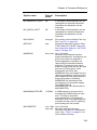
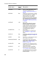
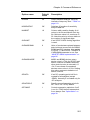
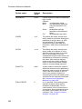
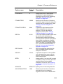
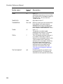
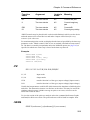
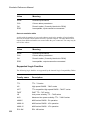
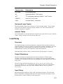
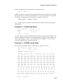
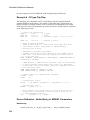
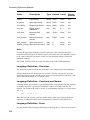
GaAsFET Model Parameters
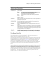
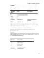
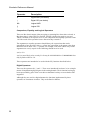
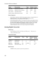
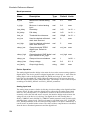
The symbols ' × ' and ' ÷ ' in the Area column means that parameter should be
multiplied or divided by the area factor respectively.
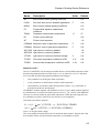
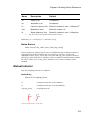
Name
Description
Units
Default Area
VTO
Pinch-off Voltage
V
-2.0
BETA
Transconductance parameter
A/V
B
Doping tail extending parameter
1/V
0.3
ALPHA
Saturation voltage parameter
1/V
2
LAMBD
A
Channel length modulation
parameter
1/V
0
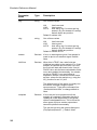
RD
Drain ohmic resistance
W
0
÷
2
2.5e-3
×
RS
Source ohmic resistance
W
0
÷
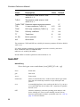
CGS
Zero bias gate source capacitance
F
0
×
CGD
Zero bias gate drain capacitance
F
0
×
PB
Gate junction potential
V
1
IS
Gate p-n saturation current
A
1e-14
FC
Forward bias depletion capacitance
coefficient
KF
Flicker noise coefficient
0
AF
Flicker noise exponent
1
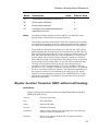
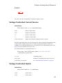
Notes
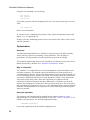
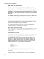
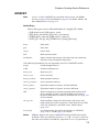
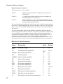
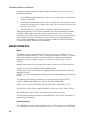
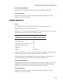
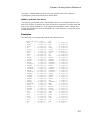
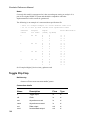
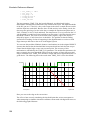
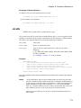
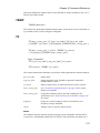
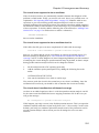
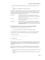
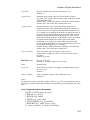
The GaAsFET model is derived from the model developed by Statz. The
DC characteristics are defined by parameters VTO, B and BETA, which
determine the variation of drain current with gate voltage, ALPHA, which
determines saturation voltage, and LAMBDA, which determines the output
conductance. IS determines the gate-source and gate-drain dc
characteristics.
×
0.5
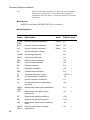
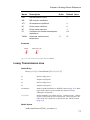
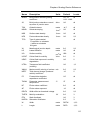
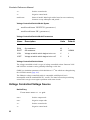
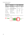
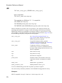
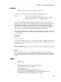
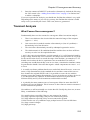
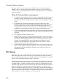
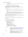
Two ohmic resistances are included. Charge storage is modelled by total
gate charge as a function of gate-drain and gate-source voltages and is
defined by the parameters CGS, CGD and PB.
69