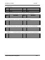
1
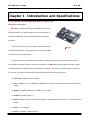
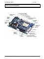
www.nexcom.com
The DigitalInfrastructure
CPU Board
EBC 569 Series
User's Manual
EBC 569 User‘s Guide
Rev. B0
Chapter 1 Introduction and Specifications
5.25" Pentium® III Level New Embedded Engine Is Ideal For New
Generation of POS Kiosk
EBC 569,a new Pentium® III-based embedded CPU board,
and claimed that it is a powerful engine for the new generation of
multimedia, networked, and panel-based POS (Point Of Sales)
machines.
This kind of POS, kiosks, or even game machines will deliver
EBC 569
vivid audio/video streams, quick responses, and real-time updates
to and from local or remote servers.
For high sales seasons, definitely need the best POS machines to attract more customers and process
more transactions with the same or even lower investment. The EBC 569, with the powerful on board, surfacemounted Pentium III compatible CPU, the richest built-in features, and various conventional specs like SIO x4,
PC 104, etc. all included, it will boost the POS kiosk and game machines to new heights.
The EBC 569 specifications are as follows:
?? CPU: C3 EBGA CPU, up to 800MHz, 133MHz FSB or VIA Eden series ultra low power CPU without fan
support
?? Memory: 512 MB SDRAM (max.), DIMMx1, PC 133 spec.
?? Chipset: VIA 8606 (Twister T)
?? VGA: S3 Savage4 on Die, 4X AGP, 2D/3D support, 32 MB shared Frame Buffer, TTL/ LVDS interface to
Panels
?? Audio: AC 97 compliant
?? LAN: 10/ 100 Base T Ethernet port x2
Introduction
1 -1
EBC 569 User‘s Guide
Rev. B0
?? Compact Flash connector x1
?? I/O: SIO x4, PIO x1, USB x2, FDD, IDE,¡K
?? Bus: PC 104 x1, PCI slot x1
?? Form Factor: 5.25" Drive foot print, 203mm x 143mm
The computing power, the audio/video capabilities, and the connectivity have become a basic requirement
for the new generation of POS machines, which means a Pentium III class of CPU is a must for the computing
functions. The trend of feeding video streams through the network to the POS/POI (Point of Information)
machines is now growing very fast. The 3D graphics, or even videos are very popular on game machines. The
DVD quality, or more specifically the MPEG II decoding capability, given that it has already become a standard
in the consumer world, is also a growing trend. People just can't live without it! The traditional embedded
solutions offered to answer these growing needs just seem a little bit awkward.
People use the discrete chips for the solutions; the Intel Pentium III CPU, with the additional VGA chip
supporting panels that have higher performance (which is still not enough), they are either too expensive or far
below the performance required. However, with NEXCOM's EBC 569, we use the low power yet high
performance C3 CPU with the same process as the Tualatin CPU (.13u), and up to 800 MHz (1GHz in the
near future), plus the chip set built with the H/W core from S3 Savage4 4X AGP video controller, 3D capability,
and 32 MB shared frame buffer. This is the new generation, highly integrated, and cost effective computing
platform for the embedded world. It just fits perfectly! With the CPU performance growing steadily on the same
design, it's a platform that promises a long term superiority.
For applications that prefer low power to high performance, the EBC 569 will be able to use the ultra low
power series of Eden CPUs starting from 400 MHz up to 667 MHz in the near future; and for the 400 MHz
version specifically, there is no need of a cooling fan on the CPU, the only requirement is for the whole chassis
solution can provide the air flow to remove the heat.
Introduction
1 -2
EBC 569 User‘s Guide
Rev. B0
Specification:
??
5.25” small form factor with Dimensions: 203mm(L) ? 143mm(W)
??
PCB : 6 Layer with double side
?? On Board CPU
??
Onboard VIA C3 Processor EBGA Package with 128KB Level 1 and 64KB Level 2 Cache
??
800MHZ CPU on board, a nd feature VIA C3 series CPU with EBGA Package
??
CPU FSB 100/133MHZ
??
CPU FANless feature By VIA Eden Series Ultra Low Power CPU and Chassis air flow.
?? Main Memory
??
One 168-pin DIMM. Support Max memory size to 512MB
?? BIOS
??
Award System BIOS
??
Advanced Power Management support
??
Optional ACPI Support
??
4M bits flash ROM
?? Chip Set
??
VIA 8606 ( Twister T ) 100 /133 MHz North Bridge
??
VIA VT82C686B PSIPC PCI SUPER-I/O INTEGRATED PERIPHERAL CONTROLLER
??
PCI V2.2 complied
?? On Board LAN
??
Realtek RTL 8139C Ethernet Controller x 2
??
Single Chip 10 /100 Base TX support, full duplex
??
Boot From LAN function
??
??
Drivers support:
DOS/Windows, Windows 95/98/2000, Windows NT, Netware, SCO Open Server 5.0,
Linux 7.2 or later, FreeBSD
RJ45 with LED connector ? 2
?? On Board Audio
??
??
VT82C686A and AC97 ver. 2.0 compliant interface, Multi-stream Direct Sound and Direct
Sound 3D acceleration
Audio interface:
CD audio in , Line in ( Internal ),
Microphone in, Speaker out ( with Amplifier )
Introduction
1 -3
EBC 569 User‘s Guide
Rev. B0
?? On Board VGA ( Hardware Disable is needed)
??
VIA 8606 Integrated Savage4 2D/3D/Video Accelerator
?? Optimized Shared Memory Architecture (SMA)
?? 8 / 16 / 32 MB frame buffer using system memory
?? Single cycle 128-bit 3D architecture
?? Full internal AGP 4x performance
?? Next generation, 128-bit 2D graphics engine
?? High quality DVD video playback
?? 2D/3D resolutions up to 1920x1440
?? 3D Rendering Features
??
Extensive LCD Support
?? 36-bit DSTN/TFT flat panel interface with 256 gray shade support
?? Integrated 110 MHz LVDS interface
?? Support for all resolutions up to 1600x1200
??
Drivers support:Windows 95/98/2000, Windows NT4.0, Win XP, Linux.
??
15Pin D-Sub VGA Output,
??
LVDS Interface Connector x 1
??
TTL LCD Interface Connector x 1
?? On Board IDE Interface
??
VIA 686B South Bridge Integrated UltraDMA-33/66/100 master mode EIDE controller
??
Support UltraDMA-33/66/100 IDE with 40 pin connector ? 1
??
Internal Compact Flash socket x 1
?? On Board Bus Expansion
??
One 32 bit/33MHZ PCI Slot support PCI Expansion.
??
PC 104
??
NEXCOM Proprietary PCI Interface
Introduction
1 -4
EBC 569 User‘s Guide
Rev. B0
?? On Chip and On Board I/O
??
SIO? 4, with 4x16C550 UARTs, 40 pin 2.0 header with housing ? 1;
one for RS422/485
??
PIO? 1, bi-directional, EPP/ECP support, 26 pin connector ? 1
??
Floppy Disk controller:34 pin connector ? 1
??
6 pin mini DIN connector ? 1, for PS/2 keyboard/mouse
??
On board USB port ? 2
??
On Board buzzer ? 1
??
Digital I/O: 8 x TTL DIO
??
On board 3 pin header for I2 C, one pin for GND
??
On board 5 pin header for IrDA Tx Rx
??
On Board 2 pin header for Reset SW
??
On Board 4 pin header for power SW ( ATX Mode )
??
Power Header x 1 for LCD Panel Backlight
??
COM reserved the RING pin to power Touch Screen LCD ( jumper select 5 or 12V or ring),
??
3 pin Power Connector for CPU FAN or Chassis FAN
??
2 Pin IDE Active LED Header
?? Real Time Clocker
??
On chip RTC with battery back up
??
External Li Battery x 1
?? Watchdog Timer
??
Watchdog timeout can be programmable by Software from 0.5 second to 64 Sec.
?? System Monitor
??
Derived from Super IO to support system monitor.
??
5 voltage (For +3.3V, +5V, +12V, Vcore and +2.5V)
??
One Fan speed
??
Two temperature
??
Drivers support:Windows 95/98, Windows NT4.0/2000
Introduction
1 -5
EBC 569 User‘s Guide
Rev. B0
?? Power Source & Power Requirements
??
??
??
6 PIN Power Input Connector
PIN Define
Voltage
Power Requirement
PIN 1
+5V
PIN 2
+5V
PIN 3
GND
--
PIN 4
GND
--
PIN 5
GND
--
6A(typical)
PIN 6
+12V
1A(Typical)
3.3V is converted from +5V.
Accessory Power Converter Cable:
1. Two 4P to 6P ( For AT Power Supply )
2. ATX Power Connector to 6P+ 2 Pin Power SW ( For ATX Power Supply )
3. Optional Power Module ( EBK DC512 )to support DC power ( 16Vdc ~ 24Vdc input )
?? Environments
??
Operating temperatures:0?C to 60?C
??
Storage temperatures:-20?C to 80?C
??
Relative humidity:10% to 90% (Non-condensing)
?? Certification
??
CE approval
??
FCC Class A
?? Module Available
Model Name Description
EBC 569
EBC 569LP
Introduction
5.25” Low Power Embedded Board with on board 800+MHZ CPU
5.25” Ultra Low Power Embedded Board with on board 400MHZ CPU
1 -6
EBC 569 User‘s Guide
Rev. B0
Chapter 2 Switches and Connectors
Jumper Setting and Pin Assignment
2-1
EBC 569 User‘s Guide
Jumper Setting and Pin Assignment
Rev. B0
2-2
EBC 569 User‘s Guide
Rev. B0
Bracket Connector
?? CON1
(PS/2
Keyboard/Mouse
Connector):
PC99
complied
purple
PS/2
connector
(4NBMF00605).
Pin No.
1
3
5
7
9
Description
Keyboard Data
Chassis Ground
Keyboard Clock
Chassis Ground
Chassis Ground
Pin No.
2
4
6
8
Description
Mouse Data
+5V
Mouse Clock
Chassis Ground
?? CON2 (USB Connector): Use PC99 complied USB dual high connector (4NBUF00202).
Pin No.
1
3
5
7
Description
+5V
USB1 Plus
+5V
USB2 Plus
Pin No.
2
4
6
8
Description
USB1 Minus
EMI Ground
USB2 Minus
EMI Ground
?? CON3 (LAN2 RJ45 Connector): Use RJ45 connector with two LED (4NBPD04503).
Pin No.
1
3
5
7
9
11
13
Description
LAN2 TX+
LAN2 RX+
PD to TERMPLANE
PD to TERMPLANE
LAN Speed# (10/100)
LAN TX/RX
Chassis Ground
Pin No.
2
4
6
8
10
12
14
Description
LAN2 TXPD to TERMPLANE
LAN2 RXPD to TERMPLANE
LED Power (VCC3)
LED Power (VCC3)
Chassis Ground
* PD Mean Pull-Down.
Jumper Setting and Pin Assignment
2-3
EBC 569 User‘s Guide
Rev. B0
?? CON4 (LAN1 RJ45 Connector): Use RJ45 connector with two LED (4NBPD04503).
Pin No.
1
3
5
7
9
11
13
Description
LAN1 TX+
LAN1 RX+
PD to TERMPLANE
PD to TERMPLANE
LAN Speed# (10/100)
LAN TX/RX
Chassis Ground
Pin No.
2
4
6
8
10
12
14
Description
LAN1 TXPD to TERMPLANE
LAN1 RXPD to TERMPLANE
LED Power (VCC3)
LED Power (VCC3)
Chassis Ground
* PD Mean Pull-Down.
?? CON5 (VGA Connector): standard 5.08mm DB-15 female connector x 1 (4NBDF01503).
Pin No.
1
3
5
7
9
11
13
15
17
Description
Red
Blue
Ground
Chassis Ground
+5V
Pull-up
Horizontal Sync.
DDC Clock
Chassis Ground
Pin No.
2
4
6
8
10
12
14
16
Description
Green
N/A
Chassis Ground
Chassis Ground
Ground
DDC Data
Vertical Sync.
Chassis Ground
?? CON6 (Line Output Connector): Use external Phone Jack connector (4NBPF00501).
Pin No.
1
3
5
Description
Ground
Right Sound Channel
NC
Pin No.
2
4
Description
Left Sound Channel
NC
?? CON7 (Microphone Input Connector): Use external Phone Jack connector (4NBPF00501).
Pin No.
1
3
5
Description
Ground
Right Sound Channel
Ground
Jumper Setting and Pin Assignment
Pin No.
2
4
Description
Left Sound Channel
Ground
2-4
EBC 569 User‘s Guide
Rev. B0
?? J1 (Line Input Connector): Use 2.0 mm 180-degree 1X4 JST connectors (4NCJM00402).
Pin No.
1
3
Description
Left Sound Channel
Ground
Pin No.
2
4
Description
Ground
Right Sound Channel
?? J2 (Primary IDE Channel Connector): Use PC99 blue 2X20 2.54mm BOXHEADER
(4NCBM04006).
Pin No.
1
3
5
7
9
11
13
15
17
19
21
23
25
27
29
31
33
35
37
39
Description
Reset #
Data 7
Data 6
Data 5
Data 4
Data 3
Data 2
Data 1
Data 0
Ground
DMA REQ
IOW#
IOR#
IOCHRDY
DMA ACK#
Interrupt 14
Disk Address 1
Disk Address 0
HDC CS100
HDD Active Led
Pin No.
2
4
6
8
10
12
14
16
18
20
22
24
26
28
30
32
34
36
38
40
Description
Ground
Data 8
Data 9
Data 10
Data 11
Data 12
Data 13
Data 14
Data 15
NC
Ground
Ground
Ground
Pull Down
Ground
NC
DMA66 Detect
Disk Address 2
HDC CS300
Ground
?? J3 (CD Input Connector): Use 2.0 mm 180-degree 1X4 JST connectors (4NCJM00402).
Pin No.
1
3
Description
Left Sound Channel
Ground
Pin No.
2
4
Description
Ground
Right Sound Channel
?? J5 (IDE Active LED Connector): 1X2 2.54mm pin header (4NCIM00201).
Pin No.
1
Description
Pull up to +5V
Jumper Setting and Pin Assignment
Pin No.
2
Description
Active signal
2-5
EBC 569 User‘s Guide
Rev. B0
?? J6 (Serial Port Connector): Use 2.0mm 2X20 box header (4NCBM04008).
Pin No.
1
3
5
7
9
11
13
15
17
19
21
23
25
27
29
31
33
35
37
39
Description
Pin No.
Data Carrier Detect A
2
Receive Data A
4
Transmit Data A
6
Data Terminal Ready A
8
Chassis Ground
10
Data Carrier Detect B (RS422/485
12
TX-)
Receive Data B (RS422/485 TX+)
14
Transmit Data B (RS422 RX+)
16
Data Terminal Ready B (RS422 RX-)
18
Chassis Ground
20
Data Carrier Detect C
22
Receive Data C
24
Transmit Data C
26
Data Terminal Ready C
28
Chassis Ground
30
Data Carrier Detect D
32
Receive Data D
34
Transmit Data D
36
Data Terminal Ready D
38
Chassis Ground
40
Jumper Setting and Pin Assignment
Description
Data set Ready A
Request to Send A
Clear to Send A
Ring Indicator A
Data set Ready B (RS422 RTS-)
Request to Send B (RS422 RTS+)
Clear to Send B (RS422 CTS+)
Ring Indicator B (RS422 CTS-)
Data set Ready C
Request to Send C
Clear to Send C
Ring Indicator C
Data set Ready D
Request to Send D
Clear to Send D
Ring Indicator D (Or +12V, +5V)
2-6
EBC 569 User‘s Guide
Rev. B0
?? J7 (NEXCOM Proprietary PCI Interface Connector): 2X34 1.27mm female connector
(4NCDF06801).
Pin No.
1
3
5
7
9
11
13
15
17
19
21
23
25
27
29
31
33
35
37
39
41
43
45
47
49
51
53
55
57
59
61
63
65
67
Description
+5V
AD1
AD3
AD5
AD7
+5V
AD9
AD11
AD13
AD15
+5V
AD17
AD19
AD21
AD23
+5V
AD25
AD27
AD29
AD31
+5V
C/BE1#
C/BE3#
FRAME#
IRDY#
+5V
DEVSEL#
SERR#
First GNT#
NC
Second PCI Clock
PCI Reset#
INTA#
INTC#
Pin No.
2
4
6
8
10
12
14
16
18
20
22
24
26
28
30
32
34
36
38
40
42
44
46
48
50
52
54
56
58
60
62
64
66
68
Description
AD0
AD2
AD4
AD6
Ground
AD8
AD10
AD12
AD14
Ground
AD16
AD18
AD20
AD22
Ground
AD24
AD26
AD28
AD30
Ground
C/BE0#
C/BE2#
PAR
TRDY#
Ground
STOP#
PERR#
First REQ#
NC
NC
First PCI Clock
LOCK#
INTB#
INTD#
?? J8 (Compact Flash Connector): Use high 2.0 mm connector (4SIPLC5001).
Pin No.
1
3
5
7
9
11
13
15
17
19
21
Description
Ground
Data 4
Data 6
HDC CS100
Ground
Ground
+5V
Ground
Ground
Disk Address 1
Data 0
Jumper Setting and Pin Assignment
Pin No.
2
4
6
8
10
12
14
16
18
20
22
Description
Data 3
Data 5
Data 7
Ground
Ground
Ground
Ground
Ground
Disk Address 2
Disk Address 0
Data 1
2-7
EBC 569 User‘s Guide
23
25
27
29
31
33
35
37
39
41
43
45
47
49
Rev. B0
Data 2
CF_CD2# (Pull-down)
Data 11
Data 13
Data 15
CF_VS1# (NC)
IOW
Interrupt 15
CF_CSEL# (Master or Slave)
Reset #
DMA REQ / DACK (NC)
HDD Active Led
Data 8
Data 10
24
26
28
30
32
34
36
38
40
42
44
46
48
50
IOCS16# (NC)
CF_CD1# (Pull-down)
Data 12
Data 14
HDC CS300
IOR
CF_WE# (+5V)
+5V
CF_VS2# (NC)
IOCHRDY
DMA ACK# /CF_REG# (+5V)
DMA66 Detect / CF_PDIAG#
Data 9
Ground
?? J9 (Digital I/O Connector): Use 2X4 2.54mm pin header (4NCIM2X401).
Pin No.
1
3
5
7
Description
Digital input 1
Digital input 2
Digital input 3
Digital input 4
Jumper Setting and Pin Assignment
Pin No.
2
4
6
8
Description
Digital output 1
Digital output 2
Digital output 3
Digital output 4
2-8
EBC 569 User‘s Guide
Rev. B0
?? J10 (PC104 Connector): Use one 2.54mm 2X20 female connector (4NCDF04001) and one
2.54mm 2X32 female connector (4NCDF06401).
2X32 female connector:
Pin No.
1(B1)
3(B2)
5(B3)
7(B4)
9(B5)
11(B6)
13(B7)
15(B8)
17(B9)
19(B10)
21(B11)
23(B12)
25(B13)
27(B14)
29(B15)
31(B16)
33(B17)
35(B18)
37(B19)
39(B20)
41(B21)
43(B22)
45(B23)
47(B24)
49(B25)
51(B26)
53(B27)
55(B28)
57(B29)
59(B30)
61(B31)
63(B32)
Description
Ground
RESET
+5V
IRQ9
-5V
DMA request 2
-12V
Zero wait state
+12V
Ground
S memory write
S memory read
I/O write
I/O read
DMA acknowledge 3#
DMA request 3
DMA acknowledge 1#
DMA request 1
Refresh#
System clock
IRQ7
IRQ6
IRQ5
IRQ4
IRQ3
DMA acknowledge 2#
Terminal count
Bus address latch enable
+5V
Oscillator (14.318MHz)
Ground
Ground
Jumper Setting and Pin Assignment
Pin No.
2(A1)
4(A2)
6(A3)
8(A4)
10(A5)
12(A6)
14(A7)
16(A8)
18(A9)
20(A10)
22(A11)
24(A12)
26(A13)
28(A14)
30(A15)
32(A16)
34(A17)
36(A18)
38(A19)
40(A20)
42(A21)
44(A22)
46(A23)
48(A24)
50(A25)
52(A26)
54(A27)
56(A28)
58(A29)
60(A30)
62(A31)
64(A32)
Description
I/O channel check#
Data7
Data6
Data5
Data4
Data3
Data2
Data1
Data0
I/O channel ready
Address enable
Address19
Address18
Address17
Address16
Address15
Address14
Address13
Address12
Address11
Address10
Address9
Address8
Address7
Address6
Address5
Address4
Address3
Address2
Address1
Address0
Ground
2-9
EBC 569 User‘s Guide
Rev. B0
2X20 female connector:
Pin No.
1(D0)
3(D1)
5(D2)
7(D3)
9(D4)
11(D5)
13(D6)
15(D7)
17(D8)
19(D9)
21(D10)
23(D11)
25(D12)
27(D13)
29(D14)
31(D15)
33(D16)
35(D17)
37(D18)
39(D19)
Description
Ground
Memory chip select 16#
I/O chip select 16#
IRQ10
IRQ11
IRQ12
IRQ15
IRQ14
DMA acknowledge 0#
DMA request 0
DMA acknowledge 5#
DMA request 5
DMA acknowledge 6#
DMA request 6
DMA acknowledge 7#
DMA request 7
+5V
Master#
Ground
Ground
Jumper Setting and Pin Assignment
Pin No.
2(C0)
4(C1)
6(C2)
8(C3)
10(C4)
12(C5)
14(C6)
16(C7)
18(C8)
20(C9)
22(C10)
24(C11)
26(C12)
28(C13)
30(C14)
32(C15)
34(C16)
36(C17)
38(C18)
40(C19)
Description
Byte high enable#
Address23
Address22
Address21
Address20
Address19
Address18
Address17
Memory read#
Memory write#
Data8
Data9
Data10
Data11
Data12
Data13
Data14
Data15
Ground
Ground
2-10
EBC 569 User‘s Guide
Rev. B0
?? J11 (32 Bits PCI Slot): Standard 32bits PCI slot (4SIPCISL02).
Pin
No.
A1
A2
Description
Test Reset#
+12V
Pin
No.
A32
A33
Description
AD16
+3.3V
Pin
No.
B1
B2
A3
A4
A5
A6
A7
A8
A9
A10
A11
A12
A13
Test Mode
Test Input
+5V
Interrupt A#
Interrupt C#
+5V
Reserved
+5V
Reserved
Ground
Ground
A34
A35
A36
A37
A38
A39
A40
A41
A42
A43
A44
Frame#
Ground
Target Ready#
Ground
Stop#
+3.3V
Snoop Done
Snoop Backoff#
Ground
Parity
AD15
B3
B4
B5
B6
B7
B8
B9
B10
B11
B12
B13
A14
A45
+3.3V
B14 Secondary Clock B45
A15
A16
A17
A18
A19
A20
A21
Secondary
GNT#
Reset#
+5V
Grant (GNT#)
Ground
PME#
AD30
+3.3V
AD17
CMD/Byte
Enable2#
Ground
Initiator Ready#
+3.3V
Device Select#
Ground
Lock#
Parity Error#
+3.3V
System Error#
+3.3V
CMD/Byte
Enable1#
AD14
A46
A47
A48
A49
A50
A51
A52
B15
B16
B17
B18
B19
B20
B21
A22
A23
A24
A25
A26
AD28
AD26
Ground
AD24
ID Select
A53
A54
A55
A56
A57
AD13
AD11
Ground
AD9
Keyway
Keyway
CMD/Byte
Enable0#
+3.3V
AD6
AD4
Ground
AD2
A27
A28
A29
+3.3V
AD22
AD20
A58
A59
A60
A30
A31
Ground
AD18
A61
A62
AD0
+5V
Request
64Bits#
+5V
+5V
Jumper Setting and Pin Assignment
Description
-12V (NC)
Test Clock
Ground
Test Output
+5V
+5V
Interrupt B#
Interrupt D#
Present1#
Secondary REQ#
Present2#
Ground
Ground
Pin
No.
B32
B33
B34
B35
B36
B37
B38
B39
B40
B41
B42
B43
B44
Description
Ground
Clock
Ground
Request#
+5V
AD31
AD29
B46
B47
B48
B49
B50
B51
B52
Ground
AD12
AD10
Ground
Keyway
Keyway
AD8
B22
B23
B24
B25
B26
Ground
AD27
AD25
+3.3V
CMD/Byte
Enable3#
B27 AD23
B28 Ground
B29 AD21
B53
B54
B55
B56
B57
AD7
+3.3V
AD5
AD3
Ground
B30 AD19
B31 +3.3V
B58 AD1
B59 +5V
B60 Acknowledge
64Bits#
B61 +5V
B62 +5V
2-11
EBC 569 User‘s Guide
Rev. B0
?? J12 (DC Adapter Board Power Input Connector): Use 1X6 3.96mm power connector
(4NCPM00605).
Pin No.
1
3
5
Description
+5V
Ground
Ground
Pin No.
2
4
6
Description
+5V
Ground
+12V
?? J13 (SMbus External Connector): Use 1X3 2.54mm pin header (4NCIM00301).
Pin No.
1
3
Description
Data
Ground
Pin No.
2
Description
Clock
?? J14 (IrDA Connector): Use 1X5 2.54mm pin header (4NCIM00501).
Pin No.
1
3
5
Description
+5V
Data Receive
Data Transmit
Pin No.
2
4
Description
No Connect
Ground
?? J16 (CPU FAN Connector): Use 1X3 2.54mm standard FAN connector (4NCJM00304).
Pin No.
1
3
Description
Ground
FAN speed sense
Chapter 1
Pin No.
1
3
5
Pin No.
2
Description
+12V
J18 (CCFL Connector): Use 1X5 2.0mm JST connector (4NCJM00506).
Description
+12V
Back light enable
+5V
Jumper Setting and Pin Assignment
Pin No.
Description
2
Ground
4
Panel back light VR (1KO)
2-12
EBC 569 User‘s Guide
Chapter 2
Rev. B0
J15 (TTL Panel Connector): Use 2X25 2.0mm BOXHEADER (4NCBM05002 or
4NCBM05003).
Pin No.
1
3
5
7
9
11
13
15
17
19
21
23
25
27
29
31
33
35
37
39
41
43
45
47
49
Description
Black Light Control
Horizontal Sync.
First Panel Clock
Data25
Data24
Data28
Data32
Data13
Data12
Data16
Data20
Ground
Data1
Data0
Data4
Data8
Ground
Data3
Data9
No Connect
Data15
Data21
Data27
Data33
Ground
Jumper Setting and Pin Assignment
Pin No.
2
4
6
8
10
12
14
16
18
20
22
24
26
28
30
32
34
36
38
40
42
44
46
48
50
Description
VEE (+12V With Control)
Data Enable
Vertical Sync.
Panel Power (5V or 3.3V)
Data31
Data26
Data30
Data34
Data19
Panel Power (5V or 3.3V)
Data14
Data18
Data22
Data7
VEE Enable
Data2
Data6
Data10
Data5
Ground
Data11
Data17
Data23
Data29
Data35
2-13
EBC 569 User‘s Guide
Rev. B0
?? J20 (LVDS Panel Connector): Use 2X7 2.0mm BOXHEADER (4NCBM01403).
Pin No.
1
3
5
7
9
11
13
Description
Panel Power (5V or 3.3V)
Data 0Data 0+
Ground
Clock +
Clock Ground
Jumper Setting and Pin Assignment
Pin No.
2
4
6
8
10
12
14
Description
Data 1Data 1+
Ground
Data 2Data 2+
Panel Power (5V or 3.3V)
Ground
2-14
EBC 569 User‘s Guide
Rev. B0
?? J21 (DIMM Connector): Use 180degree socket (4SRDI16802 or 4SRDI16803).
Pin
No.
1
3
5
7
9
11
13
15
17
19
21
23
25
27
Description
Ground
DATA1
DATA3
DATA4
DATA6
DATA8
DATA9
DATA11
DATA13
DATA14
ECC0/NC
Ground
ECC9/NC
Write Enable#
Pin
No.
2
4
6
8
10
12
14
16
18
20
22
24
26
28
Description
Pin No. Description
DATA0
DATA2
VDD
DATA5
DATA7
Ground
DATA10
DATA12
VDD
DATA15
ECC1/NC
ECC8/NC
VDD
DQ Mask0
85
87
89
91
93
95
97
99
101
103
105
107
109
111
29
31
DQ Mask1
NU/OE0#
30
32
Chip Sel.0#
Ground
113
115
33
35
37
39
41
43
45
47
Address0
Address4
Address8
Bank Sel.A1
VDD
Ground
Chip Sel.2#
DQ Mask3
34
36
38
40
42
44
46
48
117
119
121
123
125
127
129
131
49
51
53
55
57
59
61
63
65
67
69
71
73
75
77
79
81
83
VDD
ECC11/NC
ECC3/NC
DATA16
DATA18
VDD
NC
CLK Enable1
DATA21
DATA23
DATA24
DATA26
VDD
DATA29
DATA31
Clock 2
NC
I²C Clock
50
52
54
56
58
60
62
64
66
68
70
72
74
76
78
80
82
84
Address2
Address6
Address10/AP
VDD
Clock 0
NU/OE2#
DQ Mask2
NU/Write
Enable2#
ECC10/NC
ECC2/NC
Ground
DATA17
DATA19
DATA20
VREF/NC
Ground
DATA22
Ground
DATA25
DATA27
DATA28
DATA30
Ground
NC
I²C Data
VDD
Ground
DATA33
DATA35
DATA36
DATA38
DATA40
DATA41
DATA43
DATA45
DATA46
ECC4/NC
Ground
ECC13/NC
Col. Add.
Strobe#
DQ Mask5
Row Add.
Strobe#
Address1
Address5
Address9
Address11
Clock 1
Ground
Chip Sel.3#
DQ Mask7
133
135
137
139
141
143
145
147
149
151
153
155
157
159
161
163
165
167
VDD
ECC15/NC
ECC7/NC
DATA48
DATA50
VDD
NC
NC/REG En.
DATA53
DATA55
DATA56
DATA58
VDD
DATA61
DATA63
Clock 3
I²C Add. 0
I²C Add. 2
Pin
No.
86
88
90
92
94
96
98
100
102
104
106
108
110
112
Description
DATA32
DATA34
VDD
DATA37
DATA39
Ground
DATA42
DATA44
VDD
DATA47
ECC5/NC
ECC12/NC
VDD
DQ Mask4
114
116
Chip Sel.1#
Ground
118
120
122
124
126
128
130
132
Address3
Address7
Bank Sel.A0
VDD
Address12
CLK Enable0
DQ Mask6
Address13
134
136
138
140
142
144
146
148
150
152
154
156
158
160
162
164
166
168
ECC14/NC
ECC6/NC
Ground
DATA49
DATA51
DATA52
VREF/NC
Ground
DATA54
Ground
DATA57
DATA59
DATA60
DATA62
Ground
NC
I²C Add. 1
VDD
?? J22 (Reset Connector): Use 1X2 2.54mm pin header (4NCIM00201).
Jumper Setting and Pin Assignment
2-15
EBC 569 User‘s Guide
Pin No.
1
Rev. B0
Description
Reset
Pin No.
2
Description
Ground
?? J23 (Power LED Connector): Use 1X2 2.54mm pin header (4NCIM00201).
Pin No.
1
Description
Pull-Up to +5V
Pin No.
2
Description
Ground
?? J24 (Floppy Connector): Use 2X17 2.54mm box header (4NCBM02601).
Pin No.
1
3
5
7
9
11
13
15
17
19
21
23
25
27
29
31
33
Description
Ground
Ground
Ground
Ground
Ground
Ground
Ground
Ground
Ground
Ground
Ground
Ground
Ground
Ground
NC
Ground
NC (Automatic Media Sense)
Pin No.
2
4
6
8
10
12
14
16
18
20
22
24
26
28
30
32
34
Description
Drive Density Select 0
NC
Drive Density Select 1
Index Pulse Input
Motor On 0
Drive Select 1
Drive Select 0
Motor On 1
Step Direction
Step Pulse
Write Disk Data
Write Gate
Track 0
Write Protected
Read Disk Data
Head Select
Disk Change
?? J25 (Parallel Port Connector): Use 2.0mm 2X13 box header (4NCBM02602).
Pin No.
1
3
5
7
9
11
13
15
17
19
21
23
25
Description
Strobe#
Data 1
Data 3
Data 5
Data 7
Busy
Printer Select
Error#
Printer Select IN#
Chassis Ground
Chassis Ground
Chassis Ground
Chassis Ground
Pin No.
2
4
6
8
10
12
14
16
18
20
22
24
26
Description
Data 0
Data 2
Data 4
Data 6
Acknowledge
Paper Empty
Auto Form Feed#
Initialize
Chassis Ground
Chassis Ground
Chassis Ground
Chassis Ground
N/A
?? J26 (ATX Power Button Connector): Use 2x2 2.54mm pin header (4NCIM2X201).
Pin No.
1
3
Description
Power On (From ATX power)
Power On (To power button with
lock)
Jumper Setting and Pin Assignment
Pin No.
2
4
Description
Ground
Ground
2-16
EBC 569 User‘s Guide
Rev. B0
lock)
Jumper Setting and Pin Assignment
2-17
EBC 569 User‘s Guide
Rev. B0
Jumper Setting
Marked “*” was the default setting.
?? JP1 & JP2 (Fourth Serial Port RI# Pin Function Selection):
Pin No.
JP1 (1-2)
JP2 (1-2)
JP2 (2-3)
Status
Short*
Short
Short
Function Description
RI#
Select +5V
Select +12V
?? JP3 (Panel Power Select):
Pin No.
1-2
2-3
Status
Short
Short*
Function Description
+5V Input
+3.3 Input
?? JP4 (Host And PCI Frequency Select):
Frequency
133 / 33.3 MHz*
100 / 33.43 MHz
66.8 / 33.4 MHz
1-5
Open
Open
Open
2-6
Open
Open
Open
3-7
Open
Open
Short
4-8
Open
Short
Short
?? JP5 (CMOS Status Select):
Pin No.
1-2
2-3
Status
Short*
Short
Chapter 3
Function Description
Normal Operation
Clear CMOS Data
JP6 (Panel Type Select):
Jumper Setting and Pin Assignment
2-18
EBC 569 User‘s Guide
Chapter 4
Ratio
3.0X
3.5X
4.0X
4.5X
5.0X
5.5X
6.0X*
6.5X
7.0X
7.5X
8.0X
8.5X
9.0X
9.5X
10.0X
10.5X
11.0X
11.5X
12.0X
12.5X
13.0X
13.5X
14.0X
14.5X
15.0X
15.5X
16.0X
Rev. B0
JP7 (CPU Ratio Select):
1-6
(Ratio0)
Short
Short
Short
Short
Short
Short
Short
Short
Short
Short
Short
Short
Short
Short
Short
Open
Open
Open
Open
Open
Open
Open
Open
Open
Open
Open
Open
2-7
(Ratio1)
Short
Short
Short
Short
Open
Short
Open
Open
Open
Open
Open
Open
Short
Short
Short
Short
Short
Short
Short
Short
Open
Short
Open
Open
Open
Open
Open
Jumper Setting and Pin Assignment
3-8
(Ratio2)
Short
Open
Short
Open
Short
Open
Short
Open
Short
Open
Short
Open
Short
Open
Short
Open
Short
Open
Short
Open
Short
Open
Short
Open
Short
Open
Short
4-9
(Ratio3)
Short
Short
Open
Open
Short
Short
Open
Open
Short
Short
Open
Open
Short
Open
Open
Open
Short
Short
Open
Open
Short
Short
Open
Open
Short
Open
Open
5-10
(Ratio4)
Open
Open
Short
Short
Short
Short
Open
Open
Open
Open
Short
Short
Short
Open
Open
Open
Open
Open
Short
Short
Short
Short
Open
Open
Open
Short
Short
2-19
EBC 569 User‘s Guide
Chapter 5
Rev. B0
S1 & S2 (Serial Port 2 RS232/422/485 Select):
Mode
RS232*
RS422
RS485
S1-1
Off
On
On
S1-2
On
Off
Off
S1-3
Off
On
Off
S1-4
Off
Off
On
S1-5
Off
On
On
S1-6
On
Off
Off
S1-7
Off
On
On
S1-8
On
Off
Off
S1-9
Off
On
On
S1-10
On
Off
Off
Mode
RS232*
RS422
RS485
S2-1
Off
On
On
S2-2
On
Off
Off
S2-3
Off
On
On
S2-4
On
Off
Off
S2-5
Off
On
On
S2-6
On
Off
Off
S2-7
Off
On
On
S2-8
On
Off
Off
S2-9
Off
On
On
S2-10
On
Off
Off
Jumper Setting and Pin Assignment
2-20
EBC569 User‘s Guide
Rev. B0
Chapter 3 AWARD BIOS Setup
Award's BIOS ROM has a built-in Setup program that allows users to modify the basic system
configuration. This type of information is stored in battery-backed RAM (CMOS RAM) so that it
retains the Setup information when the power is turned off.
The Chapter shows the currently BIOS setup picture is for reference only, which may
change by the BIOS modification in the future. Any Major updated items or re-version, user
can download from NEXCOM web site http://www.nexcom.com.tw or any unclear message,
can contact NEXCOM Customer Service people for help
http://www.nexcom.com.tw/contact/contact.htm
??Entering Setup
Power on the computer and press <Del> immediately will allow you to enter Setup. The other
way to enter Setup is to power on the computer, when the below message appears briefly at the
bottom of the screen during the POST (Power On Self Test), press <Del> key
TO ENTER SETUP BEFORE BOOT
PRESS <DEL> KEY
??Getting Help
Main Menu
The on-line description of the highlighted setup function is displayed at the bottom of the screen.
Sub-Menu
If you find a right pointer symbol appears to the left of
certain fields (as shown in the right view), that means a
sub-menu containing additional options for the field can be
launched from this field.
To enter the sub-menu, highlight the field and press <Enter>. Then you can use control keys to
move between and change the settings of the sub-menu.
To return to the main menu, press <Esc> to trace back.
Status Page Setup Menu/Option Page Setup Menu
Press <F1> to pop up a small help window that describes the appropriate keys to use and the
possible selections for the highlighted item. To exit the Help Window press <Esc>.
BIOS Setup
3-1
EBC569 User‘s Guide
Rev. B0
??The Main Menu
Once you enter Award BIOS CMOS Setup Utility, the Main Menu (Figure 1) will appear on the
screen. The Main Menu allows you to select from ten setup functions and two exit choices.
Use arrow keys to select among the items and press <Enter> to accept or enter the sub-menu.
It is recommended to load the Defaults for “ Optimized” or “ Fail-Safe” .
Standard CMOS Features
Use this menu for basic system configuration.
Advanced BIOS Features
Use this menu to set the Advanced Features available on your system.
Advanced Chipset Features
Use this menu to change the values in the chipset registers and optimize your system's
performance.
Integrated Peripherals
Use this menu to specify your settings for integrated peripherals.
Power Management setup
Use this menu to specify your settings for power management
BIOS Setup
3-2
EBC569 User‘s Guide
Rev. B0
PNP/PCI Configuration
This entry appears if your system supports PnP / PCI.
PC health Status
Display CPU/System Temperature, Fan speed.
Load Fail-Safe Defaults
Use this menu to load the BIOS default values for the minimal/stable performance for your system
to operate.
Load Optimized Defaults
Use this menu to load the BIOS default values that are factory settings for optimal performance
system operations. While Award has designed the custom BIOS to maximize performance, the
factory has the right to change these defaults to meet their needs.
Set Supervisor Password
Enter and change the options of the setup menus. If password error or disable, some read only
INFO will be displayed on the menu.
Set User Password
Change, set, or disable password of user while posting. Switched by Security Option Item in
Advanced BIOS Features Function.
Save & Exit Setup
Save CMOS value changes to CMOS and exit setup.
Exit Without Saving
Abandon all CMOS value changes and exit setup.
BIOS Setup
3-3
EBC569 User‘s Guide
Rev. B0
??BIOS Setup Function Description
The New BIOS setup give users a more friendly information, which include all function
descriptions of BIOS setup program into the BIOS Flash ROM. When you select one function of
BIOS setup program, the function description will appeared at the right side of screen. Hence,
user doesn’t need read this manual while changing the BIOS setting.
For some critical setting or normal setting, which have no description on the Item Help
windows, user can check our Customer Service Department for detail information.
BIOS Setup
3-4
EBC569 User‘s Guide
Rev. B0
It is highly recommended to use the Default Setting for the CPU Clock Ratio and Host
Clock. If the wrong setting for the on board CPU cause the system can’t boot up, please
Clear CMOS by hardware Jumper to restore factory default value.
??Supervisor/User Password Setting
You can set either supervisor or user password, or both of then.
The differences between are:
Supervisor password
Can enter and change the options of the setup menus.
User password
Just can only enter but do not have the right to change the options of the setup
menus. When you select this function, the following message will appear at the center
of the screen to assist you in creating a password.
??ENTER PASSWORD:
Type the password, up to eight characters in length, and press <Enter>. The password typed
now will clear any previously entered password from CMOS memory. You will be asked to confirm
the password. Type the password again and press <Enter>. You may also press <Esc> to
abort the selection and not enter a password.
To disable a password, just press <Enter> when you are prompted to enter the password. A
message will confirm the password will be disabled. Once the password is disabled, the system
will boot and you can enter Setup freely.
BIOS Setup
3-1
EBC569 User‘s Guide
Rev. B0
??PASSWORD DISABLED
When a password has been enabled, you will be prompted to enter it every time you try to enter
Setup.
This prevents an unauthorized person from changing any part of your system
configuration.
Additionally, when a password is enabled, you can also require the BIOS to request a password
every time your system is rebooted. This would prevent unauthorized use of your computer.
You determine when the password is required within the BIOS Features Setup Menu and its
Security option. If the Security option is set to “System”, the password will be required both at
boot and at entry to Setup. If set to “Setup”, prompting only occurs when trying to enter
Setup.
??Power-On Boot
After you have made all the changes to CMOS values and the system cannot boot with the
CMOS values selected in Setup, restart the system by turning it OFF then ON or Pressing the
"RESET" button on the system case. You may also restart by simultaneously press <Ctrl>,
<Alt>, and <Delete> keys.
Upon restart the system, immediately press <Insert> to load BIOS default CMOS value for boot
up.
BIOS Setup
3-2
EBC569 User‘s Guide
Rev. B0
Appendix 1
Watch Dog Timer
Watch Dog Timer Working Procedure
The Watch Dog Timer (WDT) is the special hardware device. The WDT function is to monitor the computer system
whether work normally, otherwise, it will have some measures to fix up the system.
It contains a receivable SQW signal from RTC, and could set time and can clear the counter function. When time is up,
WDT can send Reset or NMI signal.
Operator has to write a value into WDT Configuration Register (Write the control value to the Configuration Port), and
clear WDT counter (read the Configuration Port).
Watch Dog Timer character and function
WDT Configuration port
F2
Default at F2
Watch Dog Timer
Disabled
1. Default at disabled
Enabled
2. Enabled for user?s programming
Reset
Default at Reset
WDT Time out active for
NMI
WDT Active Time
0.5 sec
Default at 64 sec
1 sec
2 sec
4 sec
8 sec
16 sec
32 sec
64 sec
BIOS Setup
3-3
EBC569 User‘s Guide
Rev. B0
Watch Dog Timer Control Register
The Watch Dog Timer Control Register is to control the WDT working mode. You can write the value to WDT
Configuration Port.
The following is the Control Register bit definition.
7
6
5
X
X
X
4
3
2
1
0
111 : Select 0.5 second
110 : Select 1 second
101 : Select 2 second
100 : Select 4 second
011 : Select 8 second
010 : Select 16 second
001 : Select 32 second
000 : Select 64 second
1 : Enable watch dog timer
0 : Disable watch dog timer
1 : Select NMI
0 : Select Reset
Don’t care
BIOS Setup
3-4
EBC569 User‘s Guide
Rev. B0
Watch Dog Timer Programming Procedure
? Power on or reset the system
The initial value of WDT Control Register (D4~D0) is zero, when power is on or reset the system. The
following means the initial value of WDT ( 00000000b ) :
Bit
Value
Mean
4
0
Select Reset
3
0
Disable watch dog timer
2, 1, 0
000
Select 64 second
? Initialize the SQW of RTC (set SQW output period=0.5 second)
To initialize the SQW of RTC processor is to set the SQW signal which is output period=0.5 second.
It offers the basic
frequency of the WDT counter.
The following is an example of initializing the SQW signal program in Intel 8086 assembly language.
; (Generate SQW = 0.5 Sec.)
Mov
dx, 70h
Mov
ax, 0Ah
Out
dx, al
Mov
dx, 71h
Mov
ax, 2Fh
Out
dx, al
; Out port 70h = 0Ah
; Out port 71h = 2Fh
; (enable the SQW output)
Mov
BIOS Setup
dx, 70h
Mov
ax, 0Bh
Out
dx, al
Mov
dx, 71h
Mov
ax, 0Ah
Out
dx, al
; Out port 70h = 0Bh
; Out port 71h = 0Ah
3-5
EBC569 User‘s Guide
Rev. B0
Clear the WDT
Repeatedly read WDT Configuration Port and the interval cannot be longer than the preset time, otherwise, the WDT will
generate NMI or Reset signal for the system.
The following is an example of clear the WDT program in Intel 8086 assembly language.
; ( Clear the WDT)
Mov
dx, F2h ;Setting the WDT configuration port
In
al, dx
Note: Before running WDT, you must clear the WDT. It means to make sure the initial value is zero before enabling the
WDT.
? WDT Control Register (Write to WDT configuration port)
You can set the WDT Control Register to control the WDT working mode.
The initial value of the WDT Control Register is as the following.
; (Setting the WDT Control Register as AL)
Mov
al, 0h ; Setting initial value = 0 for the WDT Control Register
You must plan the option of following:
1. Select NMI or Reset: decide D4 value in F2.
i.e. Setting D4 = 0, then it select Reset
AND
al, 11101111b ; Select Reset
i.e. Setting D4 = 1, then it select NMI
OR
BIOS Setup
al, 00010000b ; Select NMI
3-6
EBC569 User‘s Guide
Rev. B0
2. Select the time-out intervals of WDT (decide the values of D2, D1, D0 in F2 )
Example: D2~D0 = 0, the time-out interval will be 64 sec.
AND
al, 11111000b ; Setting the time-out interval as 64 sec.
3. Enable or Disable the WDT ( decide D3 value in F2)
i.e. D3=0, Disable the WDT
AND
al, 11110111b ; Disable the WDT
i.e. D3=1, Enable the WDT
OR
al, 00001000b ; Enable the WDT
After finishing the above setting, you must be output for the Control Register’s value to the WDT Configuration Port. Then
WDT will start according to the above setting.
MOV
dx, F2h
OUT
dx, al
; Setting WDT Configuration Port
; Output the Control Register
Value
? You should build in a mechanism in the program to continue to read the WDT
Configuration Port for clearing WDT before the time out.
BIOS Setup
3-7