1
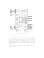
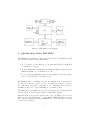
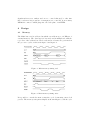
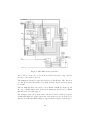
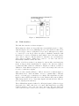
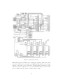
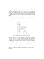
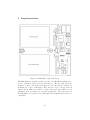
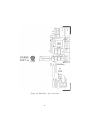
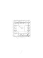
IMS B005
Design of a disk
controller board
with drives
INMOS Technical Note 15
Pete Moore
February 1987
72-TCH-015-00
You may not:
1. Modify the Materials or use them for any commercial purpose, or any public
display, performance, sale or rental;
2. Remove any copyright or other proprietary notices from the Materials;
This document is distributed in the hope that it will be useful, but WITHOUT
ANY WARRANTY; without even the implied warranty of MERCHANTABILITY
or FITNESS FOR A PARTICULAR PURPOSE.
INMOS, IMS, OCCAM are trademarks of INMOS Limited.
INMOS Limited is a member of the SGS-THOMSON Microelectronics Group.
2
Contents
1 Introduction
4
2 The
2.1
2.2
2.3
4
5
6
6
IMS M212
Memory interface . . . . . . . . . . . . . . . . . . . . . . . . .
Links . . . . . . . . . . . . . . . . . . . . . . . . . . . . . . . .
Disk interface . . . . . . . . . . . . . . . . . . . . . . . . . . .
3 Specification of the IMS B005
4 Design
4.1 Memory . . . . . . . . . .
4.2 Disk interface . . . . . . .
4.3 Phase locked loop filters .
4.4 System Control . . . . . .
4.5 Switches, links and clocks
.
.
.
.
.
.
.
.
.
.
7
.
.
.
.
.
.
.
.
.
.
.
.
.
.
.
.
.
.
.
.
.
.
.
.
.
.
.
.
.
.
.
.
.
.
.
.
.
.
.
.
5 Implementation
.
.
.
.
.
.
.
.
.
.
.
.
.
.
.
.
.
.
.
.
.
.
.
.
.
.
.
.
.
.
.
.
.
.
.
.
.
.
.
.
.
.
.
.
.
.
.
.
.
.
8
8
11
13
14
16
18
6 Design summary
19
6.1 Using the board . . . . . . . . . . . . . . . . . . . . . . . . . . 19
6.2 Software . . . . . . . . . . . . . . . . . . . . . . . . . . . . . . 20
A IMS B005 component list and PCB layout
20
References
23
3
1
Introduction
The INMOS transputer is a radical new approach to microprocessor design. To help potential users to understand its operation (and appreciate its
performance) a range of evaluation boards have been produced. These allow fast ’hands-on’ experience of the transputer and occam, the concurrent
programming language developed by INMOS to fully exploit the parallel
processing inherent in the transputer architecture.
The IMS M212 is a 16 bit transputer with a complete on-chip disk controller;
on-chip RAM provides up to five sector buffers and the on-chip ROM contains primitives needed for a disk operating system.
The IMS B005 is an extended double eurocard designed to fit into a card
frame such as the INMOS transputer evaluation module (ITEM). It has two
disk drives (a 20 MByte winchester drive and a 640 Kbyte floppy drive) as
well as all the necessary buffering for up to two additional drives, thus relieving the user of the long and expensive task of initial hardware development.
2
The IMS M212
The IMS M212 transputer disk processor is a complete computer on a chip.
It has a 16 bit processor (capable of 10 MIPS), 2 KBytes of fast (50ns cycle)
on-chip static RAM, two INMOS serial communication links (for external
communications), and a programmable external memory interface. In addition to this is a disk controller providing industry standard SA400/ST506
interfaces. The block diagram is shown in figure 1.
4
Figure 1: IMS M212 block diagram
2.1
Memory interface
The 16 bit multiplexed address/data bus of the M212 allows up to 62 KBytes
of byte organised memory, external to the transputer, as well as the 2 KBytes
of fast static RAM on the transputer chip itself. The memory map of the
M212 is signed, with the internal RAM starting at the most negative address
( Hex 8000 to Hex 87FF ). The external memory starts at Hex 8800. The
internal ROM resides at the top of the positive address space ( Hex 7000 to
Hex 7FFF), although it may be disabled if the user wishes to use external
ROM.
The internal RAM is accessible in one processor cycle (50ns), the internal
ROM in three processor cycles.
5
2.2
Links
All transputer products communicate via INMOS links; these provide pointto-point, full duplex, serial communication using a simple handshake protocol (see reference 1). The link circuit uses a direct memory access (DMA)
block transfer mechanism to pass data to and from the transputers memory, and runs concurrently with the processor, thus allowing processing to
continue during a data transfer.
The M212 has two serial links for communication with other transputer
products and one internal byte wide link to provide communication between
the processor and the disk controller hardware. This byte wide channel
appears to the processor as a normal link, but it transfers data to the disk
controller in parallel, to increase bandwidth.
2.3
Disk interface
The disk controller is designed to connect to industry standard floppy and
winchester disk drives with minimal external logic. It has two 8 bit programmable control ports and a 10 bit port for all of the special disk control
signals. These are
Vin
Phase Up
Phase Down
Early
Late
Read Data
notWriteData
notWriteGate
notIndex
WriteClock
The two 8 bit ports are used to select drives and heads as well as detection
of track0, writeprotect, writefault etc. The M212 is described in detail in
the M212 product databook [2].
A full description of the transputer architecture and occam are given in
reference [1].
6
Figure 2: IMS B005 block diagram
3
Specification of the IMS B005
The IMS B005 is designed to exploit all of the features of the M212. In this
respect there are three main requirements :
1. To be capable of controlling up to four disk drives in any combination
of winchester or floppy.
2. To have maximum external memory with the ability to switch between
RAM and ROM, or a combination of both.
3. To be compact (minimum external devices) with two drives (one winchester, one’ floppy) all on the same board.
The INMOS range of evaluation boards are mainly of the extended double eurocard form-factor (8.65” x 9.2”). To enable two drives to be fitted,
3.5” disk drives were used. Currently, a 3.5” winchester drive can store
20 MBytes, and a 3.5” floppy 640 KBytes, of formatted data.
The M212 has programmable I/O ports for selecting drives and heads, but
for more than one drive it is necessary to buffer these signals.
External memory is provided in the form of two 32 KByte by 8 devices;
these are selected by jumpers to be static RAM or EPROM. There is a wait
state generator which is switch programmable to allow for memory devices
of various access times.
7
Signals such as reset, analyse and error to control this and/or other similar boards in a larger system of transputers are controlled from a 96way
DIN41612 connector which plugs into the back plane of an ITEM.
4
4.1
Design
Memory
The M212 has a 16 bit address bus which can address up to 62 KBytes of
external memory. The data bus is 8 bits wide and is multiplexed with the
top 8 bits of the address bus. Word reads and word writes are performed in
five processor cycles, as shown in figure 3 and figure 4.
Figure 3: M212 memory timing read
Figure 4: M212 memory timing write
It is possible to extend the memory interface cycle by inserting extra clock
periods. The memory wait pin is sampled as shown in figure 5, and the cycle
8
will be extended if the wait input is high. When the wait input is sampled
low, the cycle will continue.
Figure 5: Memory wait states
The circuit diagram of the memory is shown in figure 6.
The RAM devices supplied on the IMS B005 are Hitachi HM62256P-12;
these have access times of 120ns It is also possible to use EPROM with this
interface if the user wishes to supply a custom program; suitable devices are
Hitachi HN27C256G-20, with access times of 200ns.
To enable these, and other manufacturers devices to be used, extra wait
states may be inserted by setting switch 1 positions 1 to 3. These select 1 of
8 inputs to the multiplexor IC2; with all inputs low, the inverter multiplexor
output (pin 6) is high and the memory interface must wait. The multiplexor
inputs are driven by a shift register (IC3) clocked by ProcOlockOut; when
its reset input goes high (inverse of notCE) the data (held permanently
high) is shifted into the register. Depending on which multiplexor input is
selected, it will take between 0 and 7 clock cycles for that input to go high,
sending the inverted output low and thus deasserting wait. In this way any
number of clock cycles between 0 and 7 may be inserted into the memory
cycle at the points shown in figure 5.
The complete switch settings are given in figure 13; the correct access time
may be obtained by simply adding the required number of clock periods.
With such a simple circuit it is not possible to select a different number of
wait states for top and bottom halves of memory; the interface must run at
the speed of the slowest device being use.
The top byte of the memory address bus (AD0 - AD7) is latched by ALE
(address latch enable) into the F373 (IC8), its output is permanently en9
Figure 6: IMS B005 memory interface
abled. The bottom byte of the memory address bus (A0 - A7) connects
directly to the memory devices.
The multiplexed memory data bus is driven by IC9 (F245). The direction
is controlled by RnotW (buffered by IC4), and the output enable is driven
by notCE.
The two links L2 and L3 are used to select RAM or ROM (see figure 7). In
the case of RAM AD6 is used as the most significant address bit, for ROM
RnotW is used for this purpose.
IC6 is mapped into the positive half of memory by IC5, which propagates
notCE when AD7 is low (the enable pin of the memory device is active low).
IC7 is fed notCE when AD7 is high, so appears in the negative address space.
10
Figure 7: RAM/ROM selection
4.2
Disk interface
The disk drive interface is shown in figure 8.
When using more than one floppy disk drive it is standard practice to daisychain the signal connectors, terminating the end of the chain. For this reason
only one floppy connector (JF) has been provided, although it is possible
to control up to four floppy drives if required. Similarly, winchester disk
drives have a control port which is daisy chained, hence the single winchester control connector, JW. In addition to this there are four winchester
data connectors (JDA to JDD); these connect to one drive each, and are
individually terminated inside the drive.
The two 8 bit I/O ports have been assigned to various disk control functions
in the on-chip program. Signals that are outputs to the drives are buffered
by IC10 and IC11, which are 74LS641-1. Inputs are buffered by IC12, a
74LS645-1. If the M212 is being used to control only a single drive, there is
no need to buffer these signals.
There are three switches SW2/1 to SW2/3, shown above IC10 in figure 8.
Their function is to enable the M212, on reset, to examine PA4 to PA6 and
then boot from floppy or winchester accordingly. The signal lines are held
high by resistors (RP3) and pulled low by the switches and resistors (RP2).
This arrangement does not compromise signal levels when PA4 to PA6 are
used as outputs (in normal use).
The notWriteData signal is buffered by IC4 (and again by IC10 for floppy
data) and fed to IC13; this device is a quad differential driver providing
balanced signals to each of the four data connectors. The read data from
each of the four data connectors is converted to TTL signal levels by the
11
Figure 8: Disk drive interface
differential receivers of IC14 before being gated by IC15. This device uses
the inverted DriveSelected (active low) signals (notFlopInUse for the floppy
data) to select the correct read data. Provision has been made for four
winchester drives; if all four are to be used then IC16 must be removed and
the two links L4 and L5, shown by IC15, must be made.
12
4.3
Phase locked loop filters
The M212 disk controller has, in addition to its processor clock PLL, two
additional PLLs associated with the disk controller logic. These deal with
data separation and write data precompensation:
1 Data separation: The data read from the disk is encoded using either
FM or MFM techniques, depending on the type of disk and the data
rate. A PLL is used to recover the data from the incoming bit stream.
2 Precompensation: When writing MFM data to the inner tracks of
a disk the data bits are very close together and the magnetic fields
interact during read-back. This distorts the effective position of the
stored data on the track. To compensate for this, it is necessary to
write certain bits (within a given pattern) early or late, with respect
to the normal data position. The actual value of the precompensation
is a small fraction of the write clock period; it is obtained by using
an analogue delay chain, the control voltage of which is that of a PLL
locked to a subdivision of the write clock.
In both cases, the filters required for the PLLs are off-chip to allow for
different gain and phase characteristics needed at different data rates. A
full description of the PLL filters is given in the M212 manual (reference 2)
along with examples of filter component values.
The filters are shown in figure 9. As the winchester and floppy disks have
different data rates, two filters are required, and these are switched in using
two transistors, Q1 and Q2.
Figure 9: Filter components
13
4.4
System Control
The board architecture, common to all INMOS transputer evaluation boards,
allows any number of boards to be connected together to create a multiprocessor system. On each board, the transputer links are brought to the
edge connector, and cables are used to interconnect transputers on separate
boards.
A number of control signals are also brought to the edge of the board, to
provide control over the transputer’s reset, analyse and error functions. The
system control signals are standard throughout INMOS transputer evaluation boards, and to understand the needs for the hardware to implement
these control lines, the system architecture of the boards needs to be examined. Figure 10 shows how a hierarchical network of boards can be built
into a large system.
Figure 10: Hierarchy of board connection
The Up, Down, and Subsystem ports all carry the same control signals.
These are
• notReset
• notAnalyse
• notError
The notReset and notAnalyse signals flow down the system (if the configuration of the system is considered to be as in figure 10), while the notError
14
signal flows upwards. The notAnalyse signal is used to place the system into
Analyse mode (see reference 1).
The architecture allows for any board in a chain to act as a master for
another chain, allowing large systems to be split up into smaller subsystems,
each with its own local controller. If an error occurs in the system, it can
be handled by the local controller, without interfering with the rest of the
system.
The IMS B005 is designed to be a slave processor within a larger system,
and for this reason it does not have a subsystem port. An example configuration of the IMS B005, using other INMOS evaluation boards, is shown in
figure 11.
Figure 11: Example system using the IMS B005
The Down and Up ports on the IMS B005 are implemented as shown in
figure 12. The reset and analyse switches (SW4 and SW3 respectively)
are situated on the front of the board when it is in a card frame (such as
the ITEM). The resistors and capacitors near the switches are simply for
debouncing; diode D3 is a protection device, to prevent the board from being
powered up with charge remaining on C31, thus ensuring that a power-on
reset pulse is always generated. The convention adopted by INMOS for all
evaluation boards is to use active-low signals on the ITEM backplane. IC19
and IC20 are used to produce signals of the correct sense for the transputer
and to ’or’ the transputers local signals into the chain.
The error pin also drives an LED to indicate that the error has occurred on
this board.
15
Figure 12: Up, Down and Error
4.5
Switches, links and clocks
There are several switches which have not been mentioned so far; these are
mainly concerned with the M212 functions and are shown in figure 13, along
with a description of their effect.
Figure 13: Switches
The function of the switches is shown in the table below.
Switch
Switch function
OFF
ON
1/1
1/2
1/3
1/4
MemWait 1
MemWait 2
MemWait 4
EnablelntROM
add 1 T-state
add 2 T-states
add 4 T-states
disabled
add 0 T-states
add 0 T-states
add 0 T-states
enabled
2/1
2/2
2/3
2/4
2/5
2/6
BootFromDisk
BootDriveSelect0
BootDriveSelect1
LinkSpeed
nc
BootFromLink
no auto-boot
add 0 to drive no.
winchester(drive 1)
20 Mbits/s
boot from ROM
auto-boot
add 1 to drive no.
floppy(drive 3)
10 Mbits/s
boot from link
16
The two links do not require buffering, but the link outputs are terminated
with 47 ohm resistors. The link inputs are pulled down with 100K ohm
resistors to prevent noise on unused links from causing invalid data requests.
Inputs are also protected with diodes, as shown in figure 14.
Figure 14: Links
The clocks for the board are provided by X1 and X2. X1 is a 20 MHz
crystal oscillator with a divider chain, giving 5 MHz as one of its outputs.
The M212 requires 5 MHz as an input clock.
Both winchester and floppy write data are derived from an internal write
clock, which the M212 generates from its WriteClock input. The frequencies
used are 20 MHz (X1) and 16 MHz (X2) respectively, X2 being a single
crystal oscillator package. These frequencies are higher than needed for the
write clock as they are also used in the generation of write precompensation
delays.
The clock circuits are shown in figure 15 and all other circuit components
and unused pins are shown in figure 16.
Figure 15: Clocks
Figure 16: Other components
17
5
Implementation
Figure 17: IMS B005 component layout
The IMS B005 is a four layer printed circuit board (PCB) measuring 8.65”
by 9.2” (extended double eurocard form-factor). The two disk drives are
mounted on the board as shown in figure 17. Provision has been made for
mounting two types of winchester drive and two types of floppy drive in
either position, thus it is possible to replace the floppy drive with a second
winchester drive if required by a specific application. The drives used on
the IMS B005 are as given below, although other manufacturers drives are
compatible.
18
Winchester drive
Floppy drive
NEC D3126
Olivetti HD352
NEC FD1035
TEAC FD35F
With such a large mass on the board it is necessary to use a metal plate
on the solder side of the board for strength. Also, to improve rigidity when
used in a card frame, top and bottom brackets were fixed to the exposed
sides of each drive such that they locate with adjacent guides in the card
frame. It is recommended that the board be mounted vertically due to its
high weight.
All disk drives are very sensitive to movement and vibration. In particular,
excessive shocks should be avoided. It is not advisable to remove the board
with power connected, as the disk is still spinning and a head crash may
occur.
The area under the two drives has an isolated Vcc plane (tied to ground) to
enable extra mounting holes to be drilled should the user wish to use drives
other than those recommended.
All connectors are as close to the drive connectors as possible, keeping the
cables short and neat.
6
Design summary
The IMS B005 demonstrates the ease with which the M212 can be interfaced
to disk drives. The interface requires only a small number of external devices (about 20 ICs) to implement a full four drive controller with external
memory and backplane interface, and this fits into a board area of less than
5” by 2”.
Specific user applications may not need all of this additional circuitry; indeed it is possible to control a single floppy using just the M212 (a single
winchester drive would require an 8 pin differential driver/receiver package).
6.1
Using the board
The board may be configured to boot from one of its drives by setting the
switches. The board is supplied with a test disk and the settings required
to boot from this floppy are detailed below. Alternatively, the M212 may
be booted from a link, as with other transputer devices. It is likely that the
IMS B005 would be used to boot itself from a disk and then pass boot code
from that disk to the rest of the transputer system via links.
19
SW1/1
SW1/2
SW1/3
SW1/4
OFF
ON
OFF
ON
SW2/1
SW2/2
SW2/3
SW2/4
SW2/5
SW2/6
ON
OFF
ON
OFF
ON
OFF
The use of a head ’parking’ track during transit is highly recommended, to
avoid any possible damage to data tracks.
6.2
Software
The on-chip ROM contains primitive disk routines for a disk operating system. These are fully documented in the M212 user manual (reference 2);
users may choose to expand these routines for specific applications and store
them in EPROM, or simply send them as a boot program down a link.
A
IMS B005 component list and PCB layout
Component list:
ICs
IC1
IC2
IC3
IC4,IC18,IC19
IC5,IC17
IC6,IC7
IC8
IC9
IC10,IC11
IC12
IC13
IC14
IC15
IC16
IC20
IC21
IMS M212
74F251
74F164
74F04
74F00
62256LP-10 (or 27256)
74F373
74F245
74LS641-1
74LS645-1
26LS31
26LS32
74F64
74LS14
74HCT132
74F74
20
QTY
(1)
(1)
(1)
(3)
(2)
(2)
(1)
(1)
(2)
(1)
(1)
(1)
(1)
(1)
(1)
(1)
LEDs
LED1,LED2
LED3
Crystals
X1
X2
Green (RS 588-342 or equiv)
Yellow (RS 588-358 or equiv)
16 MHz oscillator
(Euroquartz XO-1 100 or equiv)
5 and 20 MHz oscillator
(Euroquartz XO-430P 1.25MHz)
QTY
(2)
(1)
QTY
(1)
(1)
X2 is available from Euroquartz by special
order, pin2 connected to 20 MHz.
Switches
SW1
SW2
SW3
SW4
4 way DIL SPST (STC 63-20151 F)
6 way DIL SPST (STC 63-20152B)
SPDT biased (CK T108)
SPST push to make (CK TP1 1)
IC Sockets
14 pin (0.3” turned pin)
16 pin (0.3” turned pin)
20 pin (0.3” turned pin)
28 pin (0.6” turned pin)
84 pin PGA (hole in middle for
R33/C8)
QTY
(1)
(1)
(1)
(1)
QTY
(10)
(3)
(5)
(2)
(1)
Diodes
D1,D2
D3
IN6263 or 6v8 Zener
IN4148
QTY
(2)
(1)
Transistors
Q1,Q2
SD214E Mosfet or equiv
QTY
(2)
Resistor networks
RP1,RP6,RP7
RP2
RP3
RP4
RP5
4K7 8 pin 7R SIL
1K 8 pin 713 SIL
22K 8 pin 7R SIL
220R 8 pin 7R SIL
330R 8 pin 7R SIL
QTY
(3)
(1)
(1)
(1)
(1)
All resistor packs to be the same make and colour.
21
Resistors
R1,R2,R3,R4,R25
4K7
R5
680R
R6,R11,R13,R15,R23,R24 330R
R7
22K
R8
18K
R9,R10
10R
R12
1K8
R14,R18,R34,R35
100R
R16,R17
220R
R19,R20,R26,R27
100K
R21,R22
47R
R32,R33
1K
QTY
(5)
(1)
(6)
(1)
(1)
(2)
(1)
(4)
(2)
(4)
(2)
(2)
All resistors are 1/8W metal film or carbon composite
10% tolerence
Note R35 marked ’R3R’ on silk screen.
Capacitors
C28,C29,C31
C30
10uF 25V Tantalum
1uF 10V Tantalum
QTY
(3)
(1)
C11
C12
C13
C14
C15
C16
10nF (STC 17317A)
150p (STC 17299F)
6n8 (STC 43008F)
47n (STC 17319H)
330p (STC 17303B)
1nF (STC 17306G)
(1)
(1)
(1)
(1)
(1)
(1)
C11 to C16 inclusive are 5mm pitch radial ceramic
C11,C12,C14 to C16 are Vitramon VK series (STC)
C13 is STC8113 series (STC 43008F)
C1-C10,C17-C27,C32100nF multilayer ceramic
C34
All are radial with the following pitches:
4mm (2), 5mm (11), 7mm (9), 9mm (1)
Headers
JDA,JDB,JDC,JDD
JF,JW
L1,L2
Links
20way header(VERO 901-71295G)
34way header(VERO 901-71298J)
6way header(VERO 901-71292E)
0.1” links (RS 334-561)
Headers may be obtained in longer strips and split as required.
22
(24)
QTY
(4)
(2)
(2)
(4)
Plug/sockets
Floppy power
Winnie power
Backplane
Cables
Floppy power
Winnie power
4way (Amp P/N 171826-4)
4way (RS 471-430)
64way a/c DIN41612(RS 471-452)
4way plug (AMP P/N 171822-4)
Pins loose (AMP P/N 170204-2)
Pins strip (AMP P/N 170262-2)
QTY
(1)
(2)
(1)
QTY
(2)
(8)
4way socket (RS 471-424)
(2)
Floppy power con made up with 16/0.2mm (0.5 square mm) cable
Winnie power con made up with 32/0.2mm (1.0 square mm) cable
Floppy signal
Winnie Data
Winnie ctrl
34way
20way
20way
34way
34way
IDC
IDC
IDC
IDC
IDC
(RS 474-322)
(RS 474-300)
edge (RS 471-266)
(RS 474-322)
edge (RS 471-288)
(2)
(1)
(1)
(1)
(1)
All IDC connectors use ribbon cable (RS 360-122 or RS 360-166)
Screws
8mm length 6-32 UNC pan head
7mm length 4-40 UNC pan head
7mm length M3 pan head
QTY
(6)
(6)
(6)
221-CBRD-037-01
QTY
(1)
PCB
References
[1] Transputer reference manual. Published by INMOS Ltd.
Document number 72-TRN-006-02
[2] M212 reference manual. Published by INMOS Ltd.
23
Figure 18: PCB layer 1 - component side
24
Figure 19: PCB layer 4 - solder side
25
Figure 20: IMS B005 component ident
26
Figure 21: IMS M212 pinout
27