1
IMS B008 User Guide
and Reference Manual
User Manual
INMOS Limited
1990
72-TRN-223-00
You may not:
1. Modify the Materials or use them for any commercial purpose, or any public
display, performance, sale or rental;
2. Remove any copyright or other proprietary notices from the Materials;
This document is distributed in the hope that it will be useful, but WITHOUT
ANY WARRANTY; without even the implied warranty of MERCHANTABILITY
or FITNESS FOR A PARTICULAR PURPOSE.
INMOS, IMS, OCCAM are trademarks of INMOS Limited.
INMOS Limited is a member of the SGS-THOMSON Microelectronics Group.
2
Contents
1 Installation warning
5
2 Introduction
6
3 The IMS B008
6
4 Transputer, TRAMs and TRAM motherboard background
4.1 INMOS Links . . . . . . . . . . . . . . . . . . . . . . . . . . .
4.2 TRAMs . . . . . . . . . . . . . . . . . . . . . . . . . . . . . .
4.3 TRAM motherboards . . . . . . . . . . . . . . . . . . . . . .
8
8
8
9
5 TRAM slots
5.1 TRAM networks . . . . . . . . . . . . . .
5.2 The IMS C004 . . . . . . . . . . . . . . .
5.3 Network configuration processor . . . . .
5.3.1 C004 reset . . . . . . . . . . . . . .
5.4 Affect of the IMS C004 on link bandwidth
5.5 Dynamic Connection Changing . . . . . .
.
.
.
.
.
.
.
.
.
.
.
.
.
.
.
.
.
.
.
.
.
.
.
.
.
.
.
.
.
.
.
.
.
.
.
.
.
.
.
.
.
.
.
.
.
.
.
.
.
.
.
.
.
.
.
.
.
.
.
.
.
.
.
.
.
.
10
11
12
13
14
15
15
6 System services
15
6.1 Driving system services . . . . . . . . . . . . . . . . . . . . . 17
7 PC
7.1
7.2
7.3
7.4
7.5
7.6
7.7
7.8
bus interface
Link interface . . . . . . . . . . . . . . . . . . . . .
Host system services . . . . . . . . . . . . . . . . .
Interrupts . . . . . . . . . . . . . . . . . . . . . . .
DMA control . . . . . . . . . . . . . . . . . . . . .
DMA and interrupt channel selection . . . . . . . .
PC bus reset and reset to the IMS C012 . . . . . .
Programming the IMS B008 PC bus interface . . .
Operating the IMS B008 with the PC bus interface
8 Configuration
8.1 Investigating your PCs configuration . .
8.2 PC bus enable/disable and base address
8.3 DMA and Interrupt channel selections .
8.4 System services selections . . . . . . . .
8.5 Link wiring options . . . . . . . . . . . .
8.6 Link speed selections . . . . . . . . . . .
3
.
.
.
.
.
.
.
.
.
.
.
.
.
.
.
.
.
.
.
.
.
.
.
.
.
.
.
.
.
.
.
.
.
.
.
.
. . . . .
. . . . .
. . . . .
. . . . .
. . . . .
. . . . .
. . . . .
disabled
.
.
.
.
.
.
.
.
17
19
21
23
24
25
26
26
28
.
.
.
.
.
.
.
.
.
.
.
.
29
30
30
31
32
33
33
.
.
.
.
.
.
.
.
.
.
.
.
.
.
.
.
.
.
.
.
.
.
.
.
9 Example setups
34
9.1 Example 1 : Configuring an IMS B008 with a single TRAM . 35
9.2 Module Motherboard Software (MMS) . . . . . . . . . . . . . 37
9.3 Example 2 : Setting up a square network on the IMS B008 . 39
9.4 Example 3 : A cube network set up on two IMS B008 boards 42
9.4.1 Configuration of first board . . . . . . . . . . . . . . . 42
9.4.2 Configuration of the second board . . . . . . . . . . . 43
9.4.3 Completing the network . . . . . . . . . . . . . . . . . 43
10 Connectors
47
10.1 Cables . . . . . . . . . . . . . . . . . . . . . . . . . . . . . . . 48
A Unpacking, handling and installation
A.1 Unpacking and handling the IMS B008 . . . .
A.2 Installing the IMS B008 in a PC bus card slot
A.3 Installing TRAMS on the IMS B008 . . . . .
A.4 Installation of a TRAM with subsystem pins
.
.
.
.
.
.
.
.
.
.
.
.
.
.
.
.
.
.
.
.
.
.
.
.
.
.
.
.
.
.
.
.
.
.
.
.
49
49
50
51
52
B Electrical characteristics
53
B.1 Power supply requirements . . . . . . . . . . . . . . . . . . . 53
B.2 Local off board connections . . . . . . . . . . . . . . . . . . . 53
B.3 Non-Local Connections . . . . . . . . . . . . . . . . . . . . . . 53
C Physical characteristics
C.1 Mechanical details . . . . . . . . . .
C.2 Weight . . . . . . . . . . . . . . . . .
C.3 Thermal information . . . . . . . . .
C.4 Operating and storage environments
.
.
.
.
.
.
.
.
.
.
.
.
.
.
.
.
.
.
.
.
.
.
.
.
.
.
.
.
.
.
.
.
.
.
.
.
.
.
.
.
.
.
.
.
.
.
.
.
.
.
.
.
.
.
.
.
55
55
55
55
56
D Connector pin assignments
57
D.1 P1, the patch header socket . . . . . . . . . . . . . . . . . . . 57
D.2 P2, the 37 way D-type connector . . . . . . . . . . . . . . . . 57
D.3 P3, and P4 the PC bus edge connectors . . . . . . . . . . . . 57
E Jumpers
61
F Switches
62
G MMS hardwire file
64
H IMS C004 configuration messages
65
I
66
Memory Map
J IMS B008 old/new version compatibility
4
66
1
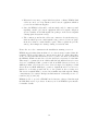
Installation warning
IMPORTANT
Read this before un-packing or operating the IMS B008
To secure correct operation of this board and to avoid possible
damage, please take the following precautions.
1. Read
Read and observe the precautions in the IMS B008 user guide and reference
manual, section A, Unpacking, Handling, and Installation and section B
Electrical Characteristics.
2. Connections to other boards
The INMOS serial links and other signals brought out to the D-connector on
the back panel of the IMS B008 are designed only to be connected to other
boards in the same electrical environment. These interconnected boards
must share a ground reference, run from similar supply voltages, and operate
in a low electromagnetic noise area. Problems should not be experienced if
the IMS B008 board is connected solely to other boards in the same PC,
using cables supplied by INMOS, and operated in a low electromagnetic
noise area. If the need arises to connect to another board in a separate
piece of equipment, then steps must be taken to ensure that the two boards
operate in the same electrical environment.
Note: the common ground reference requirement must
be met before the IMS B008 is interconnected to any
other boards even while the PC and the other systems
are powered off. Failure to observe this requirement
may result in damage to devices on the IMS B008 or
other boards.
3. Turn off first
Before plugging the IMS B008 into the PC, plugging or un-plugging any
cables to the board, or changing any switches or jumpers, ensure that the
PC and any systems to which the IMS B008 is connected are powered off.
In addition it is good practice to touch the metalwork of the PC first before touching the board or any of the cables to guard against electrostatic
discharge damage to the IMS B008 or the PC.
5
2
Introduction
This manual is intended to be used by two groups of people:
• Those users who will be using the IMS B008 in conjunction with a
standard package of software, such as the INMOS development systems
• Users who will need a greater depth of knowledge about the IMS B008,
for instance those who will be writing software that will interface directly to the board, or who will be integrating the IMS B008 into a
system.
Those in the first group should read the User guide section of the manual,
and the appendices on unpacking and installation. They will not need to
read all of the text on the PC bus interface, section 7, but the first part of
that section does give a insight into the way the interface works. Reading
these parts of the manual will give an understanding of the functions of the
IMS B008 and how to configure the board for different applications.
The second group of users should read the whole of the User guide and will
need to refer to the appendices for the additional information they require.
For those users that have previously been using earlier versions of this board,
there is an appendix on the compatibility of the IMS B008 with applications
which were designed to use earlier versions of the IMS B0081 , appendix J.
3
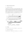
The IMS B008
The IMS B008 is a TRAansputer Module (TRAM) motherboard designed
to plug into a PC or PC/AT bus. The board has ten TRAM slots, an
interface to the PC bus2 and an IMS C004 link switch to allow networks of
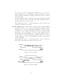
TRAMs to be set up under software control. Figure 1 identifies the major
components on the board, and figure 2 provides a functional block diagram
of the IMS B008.
The interface to the PC provides a single INMOS serial link and a system
services port. This allows software running on the PC to reset, analyse, communicate with, and monitor the error flag of a transputer network connected
1
In all of the following sections of this manual the term IMS B008 will be used to
refer to the current version of the IMS B008 which can be identified by the PCB number
221-CBRD-302-XX, where XX can be any two digits, on the top surface of the board at
the end furthest from the backpanel.
2
The term PC bus will be used throughout this manual to reference both the PC or
PC/AT busses, unless explicitly stated otherwise. PC will be used to indicate a computer
with a PC or PC/AT bus.
6
Figure 1: Top view of the IMS B008
Figure 2: Functional block diagram of the IMS B008
to or on the IMS B008. Data can be transferred to and from the link interface using programmed I/O or a DMA transfer mechanism allowing data
transfer to go on without processor intervention. On some PCs this will also
result in a faster transfer rate than can be achieved using programmed I/O.
Interrupts can be generated on link events, on error being asserted, or at
the end of a DMA transfer, freeing the processor from polling the IMS B008
to detect these events.
The TRAM slots on the IMS B008 are connected into a pipeline using two of
7
the four links from each slot. The remaining two links from slots 1 to 9 and
link 3 from slot 0 are connected to the IMS C004 link switch which allows
these links to be softwired3 together to form transputer networks other than
a pipeline. Control and configuration of the link switch is performed by an
IMS T222 16 bit transputer.
4
Transputer, TRAMs and TRAM motherboard
background
The INMOS transputer family includes 16 and 32-bit processors. These
are all capable of communicating with each other and can be programmed
when connected together to execute tasks in parallel. Full information on
transputers can be found in The Transputer Databook [1] and in other INMOS publications. The IMS B008 uses one transputer on-board for network
configuration and can support transputer arrays in the form of TRAMs.
4.1
INMOS Links
Transputers use special serial communication connections to talk to each
other. These are called INMOS links, or links. Links use two wires to
send data in two directions between two transputers (or other chips) at
up to 20 Mbits/s. All communication between TRAMs on the IMS B008,
and between the TRAMs and the PC bus interface, is via links. For full
information on links see [1] and [2].
4.2
TRAMs
TRAMs are small circuit modules which communicate via INMOS serial
links. A full TRAM background is to be found in [3]. The smallest TRAM
(called ”size 1”) is about 3 1/2” by 1” and has eight IC-type pins along
each of the short ends. These sixteen pins carry four INMOS links, reset
signals, clock and power supplies. TRAMs are plugged into a motherboard
(or baseboard) just like socketed ICs.
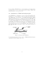
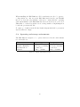
Larger TRAMs are simply a multiple of the size 1 footprint. Thus, a ”size
2” TRAM occupies two of the sockets into which a size 1 TRAM will plug.
In order to avoid confusion, discussions about motherboards (such as the
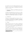
IMS B008) always refer to ”slots” (see figure 3). A slot is one position into
which a size 1 TRAM may be plugged. So, for instance, the IMS B008
3
The term softwire is used to describe a connection made between two links via a
IMS C004 link switch
8
which has ten slots, may have ten size 1 TRAMS or five size 2 or two size
4 and two size 1 or one size 8 or even six size 1 and one size 4. There is
no restriction on mixing the different sizes, as long as the total complement
will fit.
Figure 3: TRAM Slots
In addition, some TRAMs have pins which are sockets at the top. This
means that some TRAM combinations can be ”double-stacked”. For instance, if you had two size 4 (single transputer) TRAMs fitted to an IMS B008,
only two slots would actually be used for the link signals. The remaining six
slots would be covered by the TRAMs but are not used electrically. In some
cases you can plug further TRAMS into the already fitted size 4 TRAMS
and so make use of the unused slots. This double stacking is not always
possible and usually makes the board too high to fit into a single PC bus
card slot.
4.3
TRAM motherboards
A TRAM motherboard provides a number of slots into which TRAMs can be
plugged. Each of these slots provides the necessary connections to power,
clock, reset signals and the INMOS links. The motherboard provides a
method of connecting TRAMs together and may also include special circuitry to provide an interface to something other than a transputer system.
In the case of the IMS B008 this is an interface to the PC bus. The IMS B008
is one of a range of TRAM motherboards available from INMOS. All of
the INMOS motherboards have a similar architecture defined in [4]. These
motherboards can be used to build networks of transputers of arbitrary size
and are supported by a range of software products from INMOS.
It is intended that custom motherboards may be used to support TRAMs in
applications where standard motherboards are inappropriate. These moth9
erboards would provide the functions particular to the application, adding
TRAM slots to support the TRAMs required.
5
TRAM slots
The IMS B008 has ten sites for TRAMs to be plugged into called TRAM
slots. Each slot can accommodate a size 1 TRAM (see section 4.2). Larger
TRAMs will occupy more than one slot. Each of the ten slots on the
IMS B008 has connections for four INMOS links. These links will be referred to here and in the rest of this manual as slot x, link y which means
link y of slot x. Links are numbered 0 to 3 and slots, in the case of the
IMS B008, are numbered 0 to 9.
The ten slots on the IMS B008 are connected into a pipeline, using links 1
and 2 from each slot. So slot 0, link 2 is connected to slot 1, link 1; slot 1,
link 2 is connected to slot 2, link 1 and so on. These connections, and any
other link connections, made on the IMS B008 board itself are referred to
as hardwires (see section 9).
The two unconnected links, slot 0, link 1 and slot 9, link 2, at the ends of
the slot pipeline are referred to as pipehead (slot 0, link 1) and pipetail (slot
9, link 2). Pipetail is taken out to the 37 way D-type connector, P2, at the
back of the board.
In a lot of cases not all of the slots of the IMS B008 will have TRAMs
fitted, even if they are covered by a TRAM they may not be connected to
it electrically. In this case to maintain the pipeline connection pipejumpers
must be used, plugged into each un-occupied slot, or the TRAM covering
that slot. These pipejumpers connect link 1 to link 2 of the same slot.
They are plugged into the pin 1 end of the TRAM slot, with the triangle
marked on the corner. The pipejumpers have a mark on them which must
be pointing towards the pin 1 marker triangle.
The remaining two links, 0 and 3, from slots 1 to 9, and slot 0, link 3 are
connected to the IMS C004 link switch. Eight links from the IMS C004 are
taken out to the 37 way D-type connector, P2 at the back of the board.
The IMS C004 can connect together any of the links connected to its pins,
allowing networks to be set up on the IMS B008. Since link connections,
via the IMS C004, can also be made to the links coming out on P2 these
networks can extend onto multiple IMS B008s, or onto other transputer
boards, by connecting the links on P2 to the links coming out to an external
connector on the other boards. Connections between links made through
the IMS C004 are referred to as softwires (see section 9). The IMS C004
is configured by sending messages to it on its configuration link. These
10
messages are sent by the network configuration processor, an IMS T222, on
the IMS B008 (see section 5.3).
The INMOS link connections between the slots, the IMS C004, the IMS T222,
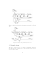
and the C012Link from the IMS C012 are shown in figure 4. Some of the
links are connected to an area labelled link jumpers in the figure. This figure
indicates the possible connections that can be made using the jumpers on
the IMS B008.
Figure 4: INMOS link connections on the IMS B008
Other connections for these links and another of the unconnected links on
the IMS C004 can be made by removing the jumpers, JP1 to JP3, and
plugging a header into P1 with the required connections wired on it (see
figure 1). Details of how to configure these jumpers and the header are
given in section 8 and examples in section 9.
5.1
TRAM networks
Using the link connections already made between the TRAMs by the pipeline
on the IMS B008 and additional link connections softwired by configuring
the IMS C004 many different networks can be set up. The choice of network
is dependent on the application. Two example networks are illustrated in
figures 5 and 6, these examples are used again to illustrate how to configure
the IMS B008 in section 9. In some cases the link connections made by
the pipeline on the board may not map onto the desired network without
making connections that are not required by the network. In this case these
11
extra connections can be ignored. An example of this could be a binary tree
network.
Figure 5: Square network
5.2
The IMS C004
The IMS C004 link switch that is used on the IMS B008 to switch links is
described in detail in The Transputer Databook [8] but will be described
briefly here. The IMS C004 has 32 link ports, between which connections
can be made. These connections are made by the IMS C004 when a message
instructing it to make a connection is received on the additional link called
ConfigLink. These messages have a simple format which tells the IMS C004,
for instance, to ”connect link a to link b” where link a and link b refer to
the links of the IMS C004. Details of the IMS C004 configuration messages
can be found in appendix H.
These configuration messages are sent to the IMS C004 by the network
configuration processor, which is an IMS T222 transputer, connected to the
ConfigLink of the IMS C004. This connection is shown in figure 4.
The IMS C004 must be hard reset after power up by pulsing the Reset pin
high for the minimum time specified in the datasheet before attempting to
send configuration data to it (see section 5.3.1).
12
Figure 6: Cube network
5.3
Network configuration processor
The network configuration processor, an 16 bit transputer the IMS T222, is
used to route configuration data on the IMS B008. With reference to figure 4,
network configuration data is received on link 1, known as ConfigUp of the
IMS T222 (referred to as the T2 for brevity) either from a TRAM in slot
0 or from another board’s network configuration processor if the board is
in a pipeline of boards. This pipeline of network configuration processors
is made in a similar way to a pipeline of TRAMS on multiple boards. The
link ConfigDown on the first board in the configuration pipeline connects to
ConfigUp on the next board and so on down the pipeline (see figure 7).
Software running on the T2 examines the configuration data for connections
to be made by the IMS C004 to which the T2 has a link connection. This
connection data is extracted from the configuration data and the connections
made by sending a set of messages to the IMS C004 via link 3 of the T2.
Configuration data for the boards further down the configuration pipeline
is then sent out on link 2 (ConfigDown).
This pipeline arrangement of T2 processors is used on all INMOS mother-
13
Figure 7: A configuration pipeline
boards that have IMS C004 link switches on them. Thus arbitrarily large
networks of mixed INMOS motherboards can be configured by sending configuration data down a single link, ConfigUp at the head of the configuration
pipeline.
5.3.1
C004 reset
The IMS C004 can be reset in two ways, one by asserting the Reset pin
causing a ”hard” reset, or by sending a Reset message to the IMS C004
causing a ”soft” reset (see appendix H).
The IMS C004 must be hard reset after power up by pulsing the Reset pin
high for the minimum time specified in the datasheet before attempting to
send configuration data to it.
The Reset pin of the IMS C004 is controlled by the IMS T222 via a circuit
connected to its external memory interface. Any write access to a memory
address external to the T2 with the bit 0 of the write data set to one will
assert the Reset pin of the IMS C004. Writing a word to an external address
with bit 0 set to zero will deassert the Reset pin. A read access to the
external address space will cause the state of the IMS C004 Reset pin to be
undefined.
This feature allows the IMS C004 to be reset independently of the TRAMs
and the PC.
14
5.4
Affect of the IMS C004 on link bandwidth
Depending upon the type of transputers on the TRAMs at both ends of a
link which passes through an IMS C004, the link bandwidth may be lower
than for a simple transputer-to-transputer connection.
For instance, two IMS T800s connected directly will give a unidirectional
link bandwidth of 1.7 Mbytes/s. However, with one IMS C004 switching that
link, the link bandwidth is 1.3 Mbytes/s. With two IMS C004s switching
the link, as is the case with some board-to-board links using IMS B008s, the
link bandwidth will be 800 Kbytes/s.
5.5
Dynamic Connection Changing
In theory it is possible to change the configuration of the IMS C004s while a
program is executing on the TRAM array. This may be useful, for example,
in a system which needs a particular network during a data gathering phase
but a completely different network during a data processing phase. Although
this is possible, it is not easy to organise and should only be attempted by
experienced users who have a complete understanding of what needs to be
done. For those who still want to proceed, here are some guidelines:
The basic idea is that providing there is no traffic on a link, you can switch
the path it takes through an IMS C004. After switching, processing can
proceed using the new network. Obviously this requires careful synchronisation between all the programs in all the TRAMs; something which is
usually achieved via the links which are being switched.
6
System services
Transputers and therefore TRAMs require three signals to be connected to
them to allow them to initialised, debugged, and so that they can signal an
error. These signals are Reset for resetting, Analyse to allow debugging, and
Error to signal an error on a transputer or TRAM. Note that the Error signal
is an output from the transputer. These three signals are collectively known
as system services. The system services for a TRAM are treated as a single
signal conceptually although they are actually three signals. The system
services are generated by the system services port on the IMS B008 PC bus
interface, or by a subsystem port on a TRAM. TRAMs with a subsystem
port have three extra connections which are made via a row of three sockets
on the underside of the TRAM. The IMS B008 has a corresponding row of
three sockets underneath the slot 0 position only. To connect the subsystem
15
port on the TRAM to the IMS B008 a strip of three double ended pins is
inserted in the sockets in the TRAM and IMS B008. This is covered in
appendix A.4.
System services for a TRAM plugged into slot 0 on the IMS B008 can come
from one of two sources, Up system services fed from another motherboard,
or the Host system services which are controlled by the system services port
of the PC bus interface. The system services fed to slot 0 are known as the
Down system services and are buffered and connected to pins of P2, the 37
way Dtype connector at the back of the IMS B008. These Down system
services can be fed to the Up system services of another motherboard.
TRAMs plugged into slots 1 to 9 on the IMS B008 can be fed with either
the same system services as the TRAM in slot 0, the Down system services,
or from the system services provided by a subsystem port on the TRAM
in slot 0, the Subsystem services. The Subsystem services are buffered and
connected to P2 allowing these system services also to be connected to the
Up system services port of another motherboard. The sources, destinations,
and switching of system services on the IMS B008 is illustrated in figure 8.
Figure 8: System services on the IMS B008
This arrangement of system services allows a hierarchy of TRAMs to be
set up on the board with the PC controlling the TRAM in slot 0, which
in turn can control the TRAMs in slots 1 to 9 if they are connected to the
subsystem port of the TRAM in slot 0. This hierarchy can be extended to
a hierarchy of boards by connecting other motherboards Up system services
port to the Down or Subsystem services connections of the previous board
16
in the hierarchy. Some example hierarchies of system services which can be
set up are shown in figure 9.
Figure 9: Examples of hierarchy between TRAMs and between motherboards
6.1
Driving system services
When controlling the system services signals it should be borne in mind that
these signals are delayed by the buffering as they go off a board, and are
filtered where they come onto a board again introducing a delay. To ensure
that the signals have time to propagate throughout a system of TRAMs
and boards allow 100 ms between assertion of a system services signal and
assuming that the signal has been asserted at every point in the system to
which it is connected.
7
PC bus interface
The PC bus has become a de-facto standard after appearing in the IBM
PC4 . IBM PC clone manufactures produce PCs with a bus compatible with
either the PC or PC/AT bus . In addition a number of other machines
that are not clones of IBM PCs also use the PC bus as this allows these
4
IBM PC is a registered trademark of the International Business Machines Corporation
17
machines to use the very large range of boards that have become available
for the bus. The IMS B008 has been designed to work when plugged into
either a PC/AT bus slot or a PC bus slot, but the number of options for
the interrupt and Direct Memory Access (DMA) channels are reduced when
plugged into a PC bus slot.
The bus interface on the IMS B008 has four functions to perform:
1. Convert the 8 bit parallel transfers on the PC bus to serial INMOS
link transfers, and vice versa.
2. Provide a system services port.
3. Control DMA transfers.
4. Generate interrupts on events on the link interface, when transputer
error has been asserted, or on DMA transfer end.
A block diagram of the PC bus interface is given in figure 10
Figure 10: PC bus interface block diagram
To allow control of these functions from software running on the PC the
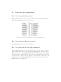
PC bus interface has a number of registers which are mapped into the I/O
address space of the PC bus, which is separate from the memory address
space. These registers are located within a thirty two byte long block of I/O
addresses decoded by the IMS B008. This thirty two byte block can have a
base address of #150, #200, or #3005 set by option switches. A memory
5
Note the # signifies a hexadecimal number.
18
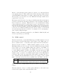
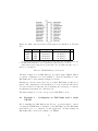
map of the registers is given in table 1. Note only nine of the thirty two
locations have registers mapped into them. Writing to the remainder of the
I/O locations will have no effect and reading these locations will result in
un-defined data being returned. The IMS B008 is however still driving the
bus when these addresses are read, this means that other boards on the PC
bus must be configured so that the I/O addresses they respond to do not
overlap this block of thirty two addresses.
Details of how these functions are performed and how they are controlled
from these registers are given in the sections following.
All transfers across the PC bus to the bus interface on the IMS B008 are
performed as byte transfers. The beard does net support 16 bit I/O transfers
en the PC/AT bus.
The PC bus interface can also be disabled, again by setting option switches,
in which case the IMS B008 does net respond to or drive any of the signals
on the bus except for the PC bus reset signal (see section 7.8).
Board
Board
Board
Board
Board
Board
Board
Board
Board
Addresses
base address
base address
base address
base address
base address
base address
base address
base address
base address
+
+
+
+
+
+
+
+
+
#00
#01
#02
#03
#10
#11
#12
#13
#14
Register
Link adapter input data register
Link adapter output data register
Link adapter input status register
Link adapter output status register
Reset/Error register
Analyse register
DMA request register
Interrupt enable register
DMA and interrupt channel select register
Table 1: PC bus interface registers memory map
7.1
Link interface
An IMS C012 link adapter is used as the basis of the link interface en the
IMS B008. Detailed information en this device can be found in [7]. This
device performs the parallel data to serial INMOS link conversions in both
directions in a similar fashion to a UART device used en an RS232 interface.
The link coming from the link adapter is labelled C012Link in figure 10.
The IMS C012 has four registers which can be written to or read by the PC
bus.
The link adapter registers function as follows:
Input Data Register holds the last data byte received from the C012Link.
19
It only contains valid data while the data present flag is set in the input status register. It can net be assumed to contain valid data after
it has been read; a double read may or may net return valid data en
the second read. If the data present flag in the input status register
is valid en a subsequent read it indicates new data is in the buffer.
Writing to this register will have no effect.
Input Status Register This register contains the data present flag (bit
0, the least significant bit) and the input interrupt enable control bit
(bit 1, the second least significant bit). The data present flag is set to
indicate that a data byte in the input data register is valid. It is reset
only when the input data register is read, or by a link reset condition
(see section 7.6) which will also reset the input interrupt enable control
bit.
When writing to this register, the data present flag and the unused
bits 27 must be written as zero bits. Note the input interrupt enable
bit does net directly control the enabling of interrupts to the PC. The
input interrupt enable bit and the data present are ”anded” together
to produce a signal labelled InputInt in figure 10. This is used to
signal to the interrupt and DMA control logic that a valid data byte is
present in the link adapter input data register. The effect of this signal
being asserted is dependent on the values written into the interrupt
and DMA control registers.
Output Data Register Data written to this register is transmitted out
of the C012Link Data must only be written to this register when the
output ready bit in the output status register is set, otherwise data
already being transmitted may be corrupted. Reading this register
results in undefined data.
Output Status Register This register contains the output ready flag (bit
0, the least significant bit) and the output interrupt enable control bit
(bit 1, the second least significant bit). The output ready flag is set to
indicate that the data output buffer is empty. It is reset only when data
is written to the output data register; it is set by a link reset condition
(see 7.6) which also resets the output interrupt enable control bit.
When writing to this register, the output ready flag and the unused
bits 27 must be written as zero bits. The output interrupt enable bit
can be set and reset by writing to the input status register (note that
the output ready flag must be written as a zero).
Again note the output interrupt enable bit does no directly control the
enabling of interrupts to the PC. The output interrupt enable bit and
the output ready flag are anded together to produce a signal labelled
OutputInt in figure 10. This is used to signal to the interrupt and
20
DMA control logic that the output data buffer in the link adapter is
empty. The effect of this signal being asserted is dependent on the
values written into the interrupt and DMA control registers.
Interrupts are explained in section 7.3.
A byte input from the C012Link proceeds as follows:
A data byte received on the C012Link is transferred into the input
data register and the data present flag set in the input status register.
If interrupts are enabled, a link data input interrupt is generated.
A processor controlling the PC bus will, either in response to the
interrupt or in a polling loop, examine the input status register. The
data present flag will be set, signifying valid data in the input data
register. The processor then reads the data byte.
If a DMA transfer from the IMS B008 to the PC memory has been set
up then the DMA logic in the PC and the control logic on the board
will transfer the data byte from the input data register to PC memory
without involving the processor.
A new data byte can now be received and the process repeats.
A byte out to the C012Link proceeds as follows:
When the output data register is empty the output ready flag will
be set in the output status register. If interrupts are enabled for this
event then an interrupt will be generated. The processor, either after
receiving an interrupt or in a polling loop, reads the output status
register. It will determine from the output ready flag that a byte may
be written to the output data register. It then writes the byte to the
output data register. The byte is transmitted on the C012Link output.
When the link adapter is next able to transmit a byte the output ready
flag will be set again.
If a DMA transfer from PC memory to the IMS B008 has been set up
then the DMA logic in the PC and the control logic on the board will
transfer the data byte from PC memory to the output data register
without intervention from the processor.
7.2
Host system services
A port is provided by the PC bus interface to allow software on the PC to
provide ”system services” to transputers connected to the IMS B008, either
as TRAMs plugged into the board or transputers on other boards. The port
appears as two registers in the I/O map of the PC and functions as follows:
Reset/Error register Bit 0 of this register controls the state of the HostReset signal. Writing a one to this bit asserts the HostReset signal caus21
ing a reset on connected transputers. Writing a zero to the bit deasserts HostReset. Note the HostReset pulse width must be a minimum of 100 ms as illustrated in figure 11. Bit 0 is cleared by the PC
bus reset signal.
Reading from this register returns the state of the notHostError signal
in bit 0. This bit is zero when the notHostError signal is asserted
(showing that an error has occurred).
Data written into bits 1 - 7 of this register has no effect, the data read
from these bits will be un-defined.
Analyse register Bit 0 of this register controls the state of the HostAnalyse signal, writing a one to this bit asserts the HostAnalyse signal.
Writing a zero to this bit de-asserts HostAnalyse. Bit 0 is cleared
by the PC bus reset signal. HostAnalyse is used, in conjunction with
HostReset, to stop a transputer connected to these signals. It allows
the internal state of the transputer to be examined so that the cause of
an error may be determined. HostReset and HostAnalyse are used as
shown in figure 12. A processor in analyse mode can be interrogated
on any of its links.
Data written into bits 1 - 7 of this register has no effect. A read from
this register will result in un-defined data being read.
Figure 11: Reset timing
Figure 12: Analyse timing
22
7.3
Interrupts
The IMS B008 can generate an interrupt en the PC bus when one of the
following events occurs:
• The end of a DMA transfer
• notHostError is asserted
• The OutputInt signal from the IMS C012 is asserted
• The InputInt signal from the IMS C012 is asserted
Generation of interrupts en each of these events is controlled by four bits in
a register, the interrupt enable register. Bits 0 - 3 of this register are used
to mask (disable) or enable interrupts for each event. Setting a bit to one
in the register enables interrupts en the event corresponding to that bit. A
table of these bits is given in table 2. The contents of bits 0 - 3 can be read
from the register. Data written into bits 4 - 7 will have no effect and a read
from this register will result in un-defined data in these bits.
The interrupt channel used by the IMS B008 to request an interrupt is
selected by two bits in the DMA and interrupt channel select register (see
section 7.5).
Note that when all the interrupt enable bits are zero the driver for the interrupt request line selected is turned off (tristated ), leaving the interrupt
request line floating, resulting in a undefined logic input to that input of
the interrupt controller in the PC. It is therefore essential that the relevant
input of the interrupt controller is disabled before the bottom four bits in
the interrupt enable register are cleared to zero. Similarly when enabling interrupts the driver en the IMS B008 must be turned en, by setting one of the
bottom four bits of the interrupt enable register to a one, before the channel
of the interrupt controller is enabled. Failure to observe this sequence of
operations may result in spurious interrupts as the floating request line may
pass through the low to high logic threshold of the input to the interrupt
controller.
Bit No.
0
1
2
3
Corresponding event
DMA end interrupt enable
Error interrupt enable
Link output interrupt enable ( OutputInt asserted )
Link input interrupt enable ( InputInt asserted )
Table 2: Interrupt enable register bit functions
23
Bits 0 - 3 of the interrupt enable register are cleared to zero when the PC bus
reset signal is asserted. This results in the all the interrupt channel drivers
en the IMS B008 being tristated, avoiding conflicts with ether beards en the
PC bus after power up and before the DMA and interrupt channel select
register has been set up.
Interrupts en the PC bus are edge triggered which means that an interrupt is
generated each time the interrupt request line en the bus makes a transition
from de-asserted to asserted. This should be borne in mind when writing
software using interrupts. For an interrupt request to interrupt the processor
in the PC the interrupt request input must correctly set up at the interrupt
controller. In most PCs this controller is an INTEL 8259A, but this may net
be the case for workstations using a PC bus. It is necessary to read in detail
about the interrupt system en your PC or workstation before attempting to
write software using interrupts.
Further details en interrupts applicable to the IBM PC, IBM PC/AT, and
clones are given in [6], [5], and [10]
7.4
DMA control
The PC bus interface en the IMS B008 supports DMA transfers between
the PC memory and the link adapter data registers only. DMA cannot be
used to transfer data to or from any ether register in the PC bus interface.
The PC bus has a number of DMA channels available and the one the
IMS B008 will use is selected by two bits in the DMA and interrupt channel
select register. To perform a DMA transfer the registers of the DMA controller, in the PC, corresponding to the channel selected need to be set up
to enable DMA transfers. Details of the DMA controller used in the IBM
PC, PC/AT, and clones can be found in [11], [6], and [5]. To initiate the
transfer a write operation to the DMA request register en the IMS B008 is
performed. Bit 0 of the byte written into this register determines the direction of transfer that the IMS B008 is set up for according to table 3, which
must be the same as the direction programmed into the DMA controller.
Bit 0
0
1
Transfer direction
From PC memory to the link adapter output data register
From the link adapter input data register to PC memory
Table 3: Direction of DMA transfer set up by a write to the DMA request
register
The data written to bits 1 - 7 of this register will have no effect and a byte
read from the register will contain undefined data.
24
Writing into the DMA request register sets a latch within the IMS B008 PC
bus interface to indicate that a DMA transfer has been requested. DMA
requests will then be generated whenever the OutputInt signal is asserted
in the case of a PC memory to link adapter output data register transfer, or
whenever InputInt is asserted in the case of transfers in the ether direction.
Since the OutputInt and InputInt signals from the IMS C012 are used to
generate the DMA requests it must be ensured that the input interrupt
enable bit in the input status register and/or the output interrupt enable
bit in the output status register are set to one to enable these outputs (see
section 7.1).
DMA transfers will continue to be requested until the TC signal en the PC
bus is active at the same time as the DMA acknowledge signal for the DMA
channel being used. TC is asserted when the transfer byte count in the
DMA controller gees to zero. At this point the DMA request latch will be
reset and the end of DMA latch set if the DMA end interrupt enable bit
is set to a one in the interrupt enable register. If the DMA end interrupt
enable bit is set to a one then an interrupt request will be generated at this
point. The interrupt is cleared and the end of DMA latch reset when the
DMA end interrupt enable bit is cleared to zero.
7.5
DMA and interrupt channel selection
Selection of the DMA and interrupt channels to be used by the IMS B008
is performed by programming four bits in the DMA and interrupt channel
select register. These bits select the DMA and interrupt channel request,
IRQ and DRQ, lines that will be driven by the IMS B008 according to the
tables 4, 5, and 6. Data written to bits 4 - 7 of this register has no effect
and will be read back as undefined. The data written into bits 0 - 3 can be
read back from the register.
Bits 0 - 3 are reset to zero when the PC bus reset signal is asserted. This
ensures that no DMA channel request lines are driven en power up avoiding
conflicts with the DMA channel drivers en ether beards en the PC bus.
It should be noted that when the IMS B008 is plugged into a PC bus as
opposed to an PC/AT bus then interrupt channels 11 and 15 and DMA
channel 0 cannot be used as these are only present en the AT bus (see
section 8.3).
The IRQ and DMA select bits are encoded as follows:
25
Bit No.
0
1
2
3
Function
IRQ channel select bit least significant bit
IRQ channel select bit most significant bit
DMA channel select bit least significant bit
DMA channel select bit most significant bit
Table 4: DMA and interrupt channel select register bit functions
Bit 1
0
0
1
1
Bit 0
0
1
0
1
IRQ channel selected
3
5
11
15
Table 5: IRQ channel selections
7.6
PC bus reset and reset to the IMS C012
The PC bus has a signal RESET DRV which is asserted when the PC is
reset. This signal is used to reset the PC bus interface en the IMS B008,
but this signal does net reset the IMS C012 or the TRAMs (see section 6).
The results of RESET DRV going active have been given in the sections
above but will be summarised here. Table 7 shows the conditions associated
with each register after RESET DRV has been asserted.
The IMS C012 is reset when the DownReset signal is asserted (see section 6).
When the link adapter is reset the contents of the input data register is undefined and the data present flag and the input interrupt enable bit are reset
in the input status register. This reset also sets the output ready flag and
resets the output interrupt enable control bit in the output status register.
The reason for the DownReset signal being used to reset the IMS C012 is
that this ensures that the devices at both ends of the C012Link are reset at
the same time.
7.7
Programming the IMS B008 PC bus interface
To be able to write programs to drive the IMS B008 using anything other
than a simple polled I/O scheme requires a knowledge of the operation of
interrupts and DMA on the PC, or workstation, for which the software is
to be written. Details for the IBM PC, PC/AT, and clones can be found in
[6], [5], [10], and [11]. In the case of a workstation refer to the manuals for
the particular machine you are working with.
Example code fragments in C to show how the PC bus interface on the
26
Bit 3
0
0
1
1
Bit 2
0
1
0
1
DMA channel selected
0
1
DMA disabled
3
Table 6: DMA channel selections
Address
Base
Base
Base
Base
+
+
+
+
#10
#11
#12
#13
Base + #14
Register
Reset/Error
Analyse
DMA request
Interrupt enable
DMA and interrupt
channel select
Conditions after
RESET DRV asserted
HostReset deasserted
HostAnalyse deasserted
DMA request latch reset
All interrupts disabled,
driver tristated
IRQ 3 selected, DMA disabled
Table 7: IBM PC bus interface register reset conditions
IMS B008 could be programmed are given below.
C define statements for board register addresses:
#define
#define
#define
#define
#define
#define
#define
#define
#define
#define
#define
BOARD_BASE 0x150
DATA_IN
DATA_OUT
(
STATUS_IN
(
STATUS_OUT
(
RESET
(
ERROR
(
ANALYSE
(
DMA_REQUEST
(
INT_ENABLE
(
INT_DMA_CHANNEL (
BOARD_BASE
BOARD_BASE
BOARD_BASE
BOARD_BASE
BOARD_BASE
BOARD_BASE
BOARD_BASE
BOARD_BASE
BOARD_BASE
BOARD_BASE
+
+
+
+
+
+
+
+
+
0x1 )
0x2 )
0x3 )
0x10 )
0x10 )
0x11 )
0x12 )
0x13 )
0x14 )
C fragments giving some examples of programming the PC bus interface:
/* some example setup routines */
void enable_out_ints( void )
{
outportb( INT_ENABLE, inportb( INT_ENABLE ) | 0x04 );
}
void enable_in_ints( void )
27
{
outportb( INT_ENABLE, inportb( INT_ENABLE ) | 0x08 );
}
void enable_error_ints( void )
{
outportb( INT_ENABLE, inportb( INT_ENABLE ) | 0x02 );
}
void disable_out_ints( void )
{
outportb( INT_ENABLE, inportb( INT_ENABLE ) & 0xfb );
}
void disable_in_ints( void )
{
outportb( INT_ENABLE, inportb( INT_ENABLE ) & 0xf7 );
}
void disable_error_ints( void )
{
outportb( INT_ENABLE, inportb( INT_ENABLE ) & 0xfd );
}
/* polled link I/O procedures */
char read_link( void )
{
while (( inportb( STATUS_IN ) & 1 ) != 1 );
return( inportb( DATA_IN )) ;
}
void write_link( char byte )
{
while (( inportb( STATUS_OUT ) & 1 ) != 1 );
outportb( DATA_OUT, byte );
}
7.8
Operating the IMS B008 with the PC bus interface disabled
By setting both the option switches SW1:1 and SW1:2 to ON (see section 8)
the PC bus interface of the IMS B008 is disabled. This is useful when the
IMS B008 is connected to another board, for instance it is the second of two
IMS B008 connected in cascade. All the ”system services” signals, Reset,
Analyse, and notError should be connected to the other board as explained
in section 6.
28
Note that an IMS B008 operated with the PC bus disabled still requires the
RESET DRV signal on the PC bus to be asserted at power up to ensure
that the DRQ and IRQ signal drivers are in the tristated condition.
If the IMS B008 is plugged into a passive connector supplying power only
then the RESET DRV signal input must be held low for correct operation
of the rest of the board. In this case no connections should be made to any
of the other bus signals to the IMS B008. The IMS C004 link switch will
have to be reset using the link configuration processor (see section 5.3.1).
8
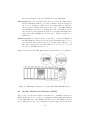
Configuration
The purpose of this section is to detail all the configuration options available
to the user.
User configurable options are set by the jumpers, JP1 to JP3, by a patch
header inserted into P1, by the bank of eight dip switches making up SW1
and by programming the DMA and interrupt channel select register. The
channel select register is covered in detail in section 7.5 and will not be
covered here.
The positions of the jumpers, patch header, and the option switches are
shown in figure 13
Figure 13: Location of the jumpers, patch header socket, and option switches
on the IMS B008
Before starting to configure the IMS B008 the user should have answered
29
the following questions so as to be able to choose which of the configuration
options are to selected.
Is the PC bus interface going to be enabled, if so what is the base address
to be set to ?
Are interrupts going to be used, if so on which channel ?
Are DMA transfers going to be used and again if so on which channel ?
What will be the source of the slot 0 system services ?
What will be the source of the slot 0 - 9 system services ?
Will one of the two link jumper settings be used, or will the patch header
be used instead ?
What link speeds will be used ?
This section seeks to help by pointing the user towards finding the information he/she needs to obtain to make these choices.
8.1
Investigating your PCs configuration
If the IMS B008 is going to be used with the PC bus interface enabled
then the configuration of the PC into which the board is to be installed
needs to be known. This involves investigating the resources used in terms
of I/O address space, interrupt channels, and DMA channels used by the
PC’s system board and the other boards plugged into the PC bus. It must
be ensured that the IMS B008 does not overlap an I/O address space used
by another board, or attempts to use an interrupt or DMA channel being
driven by any other board.
Information on the configuration of your PC can be found in the manuals for
the PC, in the manuals for each of boards plugged into the PC bus, and by
looking at these boards to determine the options actually selected on them.
8.2
PC bus enable/disable and base address
The decision as to whether to enable or disable the PC bus interface is
dependent on the use of the C012Link. If this is to be used the bus interface
must be enabled otherwise it should be disabled.
If the bus interface is enabled a decision must be taken as to the setting of
the base address. In order to make this choice it is necessary to find out
which -I/O addresses the other boards plugged into the PC bus respond
to. Having collated the addresses for the other cards choose one of the base
30
addresses for the IMS B008 such that the block of 32 I/O addresses to which
the board responds does not overlap those used by any other board. If this
is not possible it may be necessary to reconfigure some or all of the other
boards in the PC to enable this criteria to be met.
The disabling of the PC bus interface and the setting of the base address
of the IMS B008 are selected using SW1:1 and SW1:2, where SW1:1 means
SW1 bit 1, according to table 8.
SW1:1
ON
ON
OFF
OFF
SW1:2
ON
OFF
ON
OFF
Board base address
PC bus interface disabled
#150
#200
#300
Table 8: Board base address and PC bus interface disable selections
8.3
DMA and Interrupt channel selections
If the PC bus interface is to be disabled this selection does net have to be
considered of course. Otherwise the first choice is whether interrupts and/or
DMA are to be used when interfacing software to the IMS B008. This will
depend on the software to be used. The IMS B008 is supported by INMOS
software on a number of PC bus based hosts. Information on this software
can be found in the iQ Systems Databook [12]. These software packages are
supplied with manuals in which the options of using interrupts and DMA
are discussed.
If the software to be used is to be written by the user then issues such as
transfer speed and the operating system of the machine need to be considered
in writing a driver for the IMS B008. These issues are touched en in section 3.
Details of how to programme the IMS B008 to use DMA and interrupts
channels are covered in sections 7.3, 7.4, and 7.5.
Again the choice of interrupt or DMA channel to be used may well be
dictated by the boards that are already in the PC. Note that it some cases
it may net be possible to use interrupts and/or DMA with the IMS B008 as
the number of channels en the PC bus is limited and they may all be in use
by ether boards.
Having determined the channel(s) to be used the software will need to be
configured to use these. See the software manuals for details of how to de
this. Normally this software will then write into the DMA and Interrupt
channel selection register to set the IMS B008 to use these channels. If
software needs to be used that was written for elder versions of the IMS B008
31
en which the DMA and interrupt channels were selected using DIP switches
then a small programme will need to be run first to set up the DMA and
Interrupt channel selection register (see section J).
Note that the possible selections of DMA and interrupt channels that can
be used are reduced when the IMS B008 is plugged into a PC as opposed
to an AT bus slot. The possible interrupt and DMA channel selections for
the IMS B008 when it is plugged into a PC bus slot or an AT bus slot are
tabulated in table 9.
Bus slot type
PC bus
PC/AT bus
Interrupt channels
3 and 5
3, 5, 11, and 15
DMA channels
1 and 3
0, 1, and 3
a
a
Note that DRQ0 is not available on the PC bus, DRQ3 and IRQ5 are used by the
fixed disk drive in a PC/XT.
Table 9: DMA and interrupt channel selections on the two types of PC bus
8.4
System services selections
The options for the system services signals fed to slot 0 and to slots 1 to
9 were covered in section 6. Choice of the system services scheme to be
used will depend en the application. The INMOS board support software
packages and development tools may impose a particular scheme. Consult
the manuals that come with these software packages for details.
The system services options are controlled by two DIP switches, SW1:3 and
SW1:4 according to tables 11 and 8.3.
SW1:3
ON
OFF
TRAM slot 0 and DOWN system services
From Up system services
From Host system services
Table 10: Selections for slot 0 and Down system services
SW1:4
ON
OFF
TRAM slots 1 - 9 system services
From TRAM in slot 0 Subsystem services
From Down system services
Table 11: System services selections for slots 1 to 9
32
8.5
Link wiring options
Connections for the C012Link, two links from slot 0, two links from the
T2, two links from the IMS C004, and the two patch links from P2 are
determined by the jumpers JP1 and JP2 or by the patch header wiring.
The figures 14 and 15 show the connections that installing jumper sockets
on JP1 or JP2 make. When jumper sockets are present en the pins of JP3
then the pipeline connection between slots 3 and 4 is made. Appendix E
shows how the jumper sockets should be fitted to the jumper pins.
If one of the set of link connections made by JP1 or JP2 is not the desired
configuration then the jumper sockets en JP1 to JP3 should be removed and
a wired patch header plugged into P1. The pinout of this socket is given in
figure 16. This patch header allows any of the links connected to P1 to be
connected to any ether. For instance the IMS B008 can be used as a link
adapter beard for the PC by bringing the C012Link out to P2. This can
be achieved by wiring C012Link to PatchLink1 as shown in table 12. Note
that for the patch links only, the LinkIn of another link to be connected to a
patch link is connected to PatchLinkIn and LinkOut to PatchLinkOut. For
any other link on the patch header LinkIn of one link should be connected
to LinkOut of the ether link and vice versa.
From pin No.
1
2
To pin No.
18
17
Signals connected
C012LinkIn and PatchLinkIn1
C012LinkOut and PatchLinkOut1
Table 12: Example patch header wiring to connect C012Link directly to P2
8.6
Link speed selections
Link speed selections are controlled by the switches SW1:5 to SW1:8. Switches
SW1:5 and SW1:6 control the LinkSpeedB and LinkSpeedA pins respectively
on the TRAM slots. With the range of INMOS TRAMS these switches give
the link speeds shown in table 13. SW1:6 also controls the link speeds of
the IMS C012, the IMS C004, and in conjunction with SW1:7 and SW1:8
the link speeds of the IMS T222. These link speed selections are shown
in tables 14. Note for a link to operate between two devices the same bit
rate must be set at both ends. Not all combinations of the four link speed
switches will result in a set of link speeds which will allow the IMS B008 to
operate correctly.
33
Figure 14: Link connections made when jumpers are installed on JP1 and
JP3
Figure 15: Pinout of the patch header socket, P1
9
Example setups
The purpose of this section is to give examples of a IMS B008 configured in
three different ways to illustrate some of the points made in the the other
sections of this document.
34
Figure 16: Link connections made when jumpers are installed on JP2 and
JP3.
SW1:5
ON
OFF
ON
OFF
SW1:6
ON
ON
OFF
OFF
Link 0 speed
10 Mbits/s
10 Mbits/s
20 Mbits/s
20 Mbits/s
Links 1 - 3 speed
10 Mbits/s
20 Mbits/s
10 Mbits/s
20 Mbits/s
a
b
a
Note that this switch setting results in an inoperable link 3 since this link is connected
to the IMS C004 which will be set to 10 Mbits/s by this setting (see table 14).
b
This switch setting results in an inoperable link 3 since the IMS C004 will be set to a
link speed of 20 Mbits/s.
Table 13: TRAM link speed selections
The first example is a an IMS B008 set up with a single TRAM. This is
a common configuration for users wishing to check the installation of the
IMS B008 and to start running transputer software.
Example two shows a network set up on a single IMS B008, in this case a
square. The configuration of the hardware is covered and the Module Motherboard Software is briefly introduced including the setting up of softwires
and hardwires information for this network.
The final example is of a cube set up on two IMS B008 boards.
9.1
Example 1 : Configuring an IMS B008 with a single
TRAM
Before installing the IMS B008 in the PC two operations must be carried
out; first the TRAM must be installed on the IMS B008, and the IMS B008
itself will need to be configured for this application. In this example an
IMS B404 will be used as an example of a TRAM.
35
SW1:6
SW1:7
SW1:8
ON
ON
ON
ON
OFF
OFF
OFF
OFF
ON
ON
OFF
OFF
ON
ON
OFF
OFF
ON
OFF
ON
OFF
ON
OFF
ON
OFF
C012 and
C004
10 Mbits/s
10 Mbits/s
10 Mbits/s
10 Mbits/s
20 Mbits/s
20 Mbits/s
20 Mbits/s
20 Mbits/s
T2
Link0
10 Mbits/s
5 Mbits/s
10 Mbits/s
20 Mbits/s
10 Mbits/s
5 Mbits/s
10 Mbits/s
20 Mbits/s
T2
Link123
10 Mbits/s
10 Mbits/s
10 Mbits/s
10 Mbits/s
5 Mbits/s
5 Mbits/s
20 Mbits/s
20 Mbits/s
a
a
a
Note these switch settings will result in the T2 not being able to send configuration
messages to the IMS C004 link switch.
Table 14: IMS C012, IMS C004, and IMS T222 link speed selections
First follow the instructions on how to handle the IMS B008 and install a
TRAM. These are covered in section A and will not be covered here. The
most sensible slot into which to plug a single TRAM on an IMS B008 is slot
0. It is also a good idea to install the subsystem pins into the bottom of the
TRAM before plugging it into the IMS B008, if the TRAM has subsystem
capability (see section 6). This will save installing them later should it
be desired to use this single TRAM to control a network of TRAMs, such
as in the next example. When plugging in the TRAM be sure that the
orientation is correct as a mistake can cause damage to both the TRAM
and the IMS B008.
Next the IMS B008 needs to be configured for this application. Let us say
that we have determined that the only other board in the PC/AT we are
using is configured to respond to I/O addresses in the range #300 to #31
F and uses interrupt channel 3 and DMA channel 3. The IMS B008 can
be configured to a base address of #150 by setting switches SW1:1 to on
and SW1:2 to off. The DMA and interrupt channel select register can be
programmed to select interrupt channel 5 and DMA channel 0 after the PC
has been powered up without clashing with the other board. As mentioned
in section 7.5, this register will either be set up by the driver software for
the IMS B008 or by a small initialisation programme.
The other options will need to be set as follows:
Link wiring options Since we will want to communicate with the TRAM
in slot 0, the C012Link will need to be connected to the TRAM. This
can be done by putting six jumpers onto the pins marked JP1, as shown
in figure 17, which will connect Link 0 of the TRAM to C012Link.
Connections are also made between Link 1 of the TRAM and the T2,
36
and between Link 0 of the T2 and Link 28 of the IMS C004.
Link speeds Since the only link being used is between the link adapter
and the TRAM and this is over a short distance then the link speed
can be set to 20 Mbit/s. This is done by setting SW1:5 to SW1:8 to
off. Note that for simple networks set up on one or two IMS B008s in
a PC all link speeds can set to 20 Mbits/sec. The other link speeds are
only used in special applications such as connecting links using fibre
optics where the maximum speed that can be achieved easily is 5 or
10 Mbits/s.
System services To enable software on the PC to control the TRAM on
the IMS B008 the system services from the TRAM should be set to
come from the Host system services by setting switch SW1:3 to off.
The other system services switch SW1:4 does not need to be set as
there are no TRAMs in slots 1 to 9.
Figure 17 shows how the IMS B008 will look when it has been configured.
Figure 17: IMS B008 configured for a single IMS B404 TRAM in slot 0
9.2
Module Motherboard Software (MMS)
Before going onto the next example a standard piece of INMOS software, the
MMS, is introduced as one way of configuring the IMS C004 link switches
on the IMS B008 and other INMOS motherboards. The MMS is used in
these examples as a way of specifying the softwired link connections in the
37
networks. No details will be given here as to how this software is installed
or run as this can vary with different host environments and different development tools. All that needs to be grasped here is an understanding of
how the MMS works and determines the configuration information to send
to the IMS C004s on a motherboard or boards.
The MMS gains knowledge on the particular boards that are to be configured from the hardwires information given to it. This information includes
what is called a sizes section which contains details of how many T2 network configuration processors are on a board, how many IMS C004s, how
many slots, and how many edge links (link connections going off the board) .
The rest of the information is about the fixed connections on the board, the
hardwires which include any link wiring options that have been configured.
The sizes and hardwires sections together form a definition of a board which
is given a name. Several of these definitions would be used to define the set
of boards to be configured. The final part of the information tells the MMS
the order of the boards when they have been connected in a configuration
pipeline. Note that this pipeline has nothing to do with any pipelines of
TRAMs that may be set up by the boards. All this information together,
the board definitions and the PIPE statement are called the hardwires information. Examples are given below and the hardwires information for a
single IMS B008 is given in appendix G.
The desired softwired link connections through the IMS C004 on each board
are given to the MMS by lines of softwire information. These are grouped
into those for each board identified by the keyword PIPE X where X is the
position of the board in the configuration pipeline, numbering the first board
in the pipeline as 0. Example softwire information is given in the examples
below.
From the hardwires and softwires information the MMS software can boot
up the T2 transputers on each board and determine what configuration
information to send down the configuration pipeline. As the information
gets to each T2 it extracts the configuration for the IMS C004 to which it is
connected and passes on the information to the next T2 in the pipeline. Note
that the MMS does not know about, check, or care about link connections
made between the boards via the edge links.
The MMS is documented in the manuals that come with the software, and
where details can also be found on how the softwires and hardwires information is passed to the MMS.
Note that using the MMS is not the only method of configuring the IMS C004s
on INMOS motherboards. Software can be written to do this which will set
up a particular set of connections, or which performs dynamic link switching
as mentioned in section 5.5.
38
9.3
Example 2 : Setting up a square network on the IMS B008
This example will show how to set up the square network shown in figure 18
using four IMS B404 TRAMs controlled by a IMS B404 in slot 0.
Figure 18: Square network
Assuming that the IMS B404 is already installed in slot 0 with the subsystem
pins in place beneath it, as described in the first example, the rest of the
TRAMs can be plugged into slots 1, 2, 3, and 8. The TRAM in slot 8 will
need to have the spacer strips on its pins left on so that the the underside
of the TRAM clears the components under slot 9. Pipe jumpers need to
be inserted into slots 4, 5, 6, and 7 to connect the pipeline through to slot
8. This is achieved by plugging the pipejumpers into the socket pins of the
TRAMs covering these slots.
The configuration options are the same as the first example except that
the system services for the TRAMs in slots 1 to 3 need to come from the
subsystem port of slot 0 since the IMS B404 in slot 0 is to control the square.
To do this SW1:4 must be set to on.
The configuration of the PC bus interface will be left the same as in the
previous example.
Jumper JP3 must also have two jumpers placed over its pins to complete
the pipeline between slots 3 and 4.
The IMS B008 will look like figure 19 when it has been configured.
To set up the square network the four links connecting the four TRAMs need
39
Figure 19: Configuration of a IMS B008 for a square network
to be made. Three of these and the connection to the controlling TRAM
are made by the pipeline connections on the board. The fourth link to
complete the square must be made using a softwire connection. To do this a
hardwires description of the configured IMS B008 and the required softwire
must be passed to the MMS software. This information, in the hardwires
and softwires description languages as defined in the MMS documentation.
Softwires information to complete the square network:
SOFTWIRE
PIPE 0
SLOT 1, LINK 3 TO SLOT 8, LINK 0
END
Hardwires information for IMS B008 configured for example 2:
-- B008 hardwire description
DEF B008
SIZES
T2 1
C4 1
SLOT 10
EDGE 10
END
T2CHAIN
T2 0, LINK 3 C4 0
40
END
HARDWIRE
SLOT 0,LINK 2 TO SLOT 1,LINK 1
SLOT 1,LINK 2 TO SLOT 2,LINK 1
SLOT 2,LINK 2 TO SLOT 3,LINK 1
SLOT 3,LINK 2 TO SLOT 4,LINK 1
SLOT 4,LINK 2 TO SLOT 5,LINK 1
SLOT 5,LINK 2 TO SLOT 6,LINK 1
SLOT 6,LINK 2 TO SLOT 7,LINK 1
SLOT 7,LINK 2 TO SLOT 8,LINK 1
SLOT 8,LINK 2 TO SLOT 9,LINK 1
C4 0,LINK 10 TO SLOT 0,LINK 3
C4 0,LINK 1 TO SLOT 1,LINK 0
C4 0,LINK 11 TO SLOT 1,LINK 3
C4 0,LINK 2 TO SLOT 2,LINK 0
C4 0,LINK 12 TO SLOT 2,LINK 3
C4 0,LINK 3 TO SLOT 3,LINK 0
C4 0,LINK 13 TO SLOT 3,LINK 3
C4 0,LINK 4 TO SLOT 4,LINK 0
C4 0,LINK 14 TO SLOT 4,LINK 3
C4 0,LINK 5 TO SLOT 5,LINK 0
C4 0,LINK 15 TO SLOT 5,LINK 3
C4 0,LINK 6 TO SLOT 6,LINK 0
C4 0,LINK 16 TO SLOT 6,LINK 3
C4 0,LINK 7 TO SLOT 7,LINK 0
C4 0,LINK 17 TO SLOT 7,LINK 3
C4 0,LINK 8 TO SLOT 8,LINK 0
C4 0,LINK 18 TO SLOT 8,LINK 3
C4 0,LINK 9 TO SLOT 9,LINK 0
C4 0,LINK 19 TO SLOT 9,LINK 3
C4 0,LINK 20 TO EDGE 0
C4 0,LINK 21 TO EDGE 1
C4 0,LINK 22 TO EDGE 2
C4 0,LINK 23 TO EDGE 3
C4 0,LINK 24 TO EDGE 4
C4 0,LINK 25 TO EDGE 5
C4 0,LINK 26 TO EDGE 6
C4 0,LINK 27 TO EDGE 7
-- Uncomment the next two lines if the
-- patch header wiring is used to
-- connect C004, link 28 to PatchLink0,
-- and C004, link 29 to PatchLink1.
-- C4 0,LINK 28 TO EDGE 8
-- C4 0,LINK 29 TO EDGE 9
END
PIPE B008 END
41
9.4
Example 3 : A cube network set up on two IMS B008
boards
This final example shows how to configure two IMS B008 boards to be used
together to support a network of eight TRAMs controlled by a ninth TRAM
in slot 0.
IMS B404 TRAMs will be used for the TRAMs at the vertices of the cube,
and the controlling TRAM. Figure 20 shows the necessary link connections
for the cube and how these are mapped onto the link connections on the
two boards.
Figure 20: Cube TRAM network mapped onto two IMS B008 boards
9.4.1
Configuration of first board
The configuration of the first board is the same as that for the previous
example except that an additional pipejumper needs to be plugged into slot
9. This pipejumper connects slot 8 link 2 to pipetail.
42
9.4.2
Configuration of the second board
The configuration of the second board is quite different to the first and is
as follows:
The TRAMs should be plugged into slots 0 to 3. No subsystem pins are
needed underneath the TRAM in slot 0 as the subsystem will not be used.
PC bus interface The PC bus interface on this second IMS B008 is not
required and should be disabled by setting both SW1:1 and SW1:2
to on. Note that this second bus interface could be used as a way of
increasing the data rate that would be achievable between the PC and
the transputer network by providing a second link interface.
Link wiring options The connections to the Pipehead and ConfigUp links
on this board need to be connected to links coming from the first board.
To do this these links need to be brought out to the connector P2. If
jumpers are put onto the pins of JP2 then this will connect Pipehead
(slot 0, link 1) to PatchLink1, ConfigUp (T2, link 1) to PatchLink0,
and slot 0, link 0 to the IMS C004, link 28 which gives the desired
connections out to P2.
System services Since this board will be controlled from the subsystem
services of the first IMS B008 the system services for all the TRAMs
on this IMS B008 need to be connected to the Up system services.
This is done by setting SW1:3 to on selecting the Up system services
to be connected to the Down system services and slot 0, and setting
SW1:4 to off selecting the Down system services to be connected to
slots 1 to 9.
Link speeds The link speeds will need to be the same as on the first board,
20 Mbits/s, set by SW1:5 to SW1:8 being set to off.
The second IMS B008 is shown configured in figure 21
9.4.3
Completing the network
To complete the network a cable needs to be used to connect the links and
system services between the two boards. The connections required in this
cable are shown in table 15.
Finally the boards need to be installed in the PC, powered up, and the MMS
or some other software run to configure the link switches on each board. The
information required by the MMS software to do this is given below. Notice
43
Figure 21: Configuration of the second IMS B008 for the cube network
that the hardwires descriptions for the first and second IMS B008 are not
the same as different links are connected by the jumpers JP1 and JP2.
Softwires information to connect up the eight TRAMs into a cube:
SOFTWIRE
PIPE 0
SLOT 1, LINK
SLOT 2, LINK
SLOT 3, LINK
SLOT 8, LINK
PIPE 1
SLOT 1, LINK
SLOT 2, LINK
SLOT 3, LINK
SLOT 3, LINK
END
3
0
0
3
TO
TO
TO
TO
EDGE
EDGE
EDGE
SLOT
0
1
2
1, LINK 0
3
3
0
3
TO
TO
TO
TO
EDGE
EDGE
EDGE
SLOT
2
1
0
0, LINK 0
Hardwires information for the two IMS B008 used for the third example:
DEF B008ONE
SIZES
T2 1
C4 1
SLOT 10
EDGE 10
END
44
Pin No. P2
Board 1
1
5
12
27
33
15
34
36
Pin No. P2
Board 2
1
5
12
27
20
2
21
31
17
13
35
32
16
14
22
3
23
4
6
24
3
22
4
23
24
6
Signals connected
GND and GND
GND and GND
GND and GND
GND and GND
notSubSystemReset and notUpReset
notSubSystemAnalyse and notUpAnalyse
notSubSystemError and notUpError
ConfigDownLinkIn and PatchLinkOut0
(ConfigUpLinkOut)
ConfigDownLinkOut and PatchLinkIn0
(ConfigUpLinkIn)
PipetailLinkIn and PatchLinkOut1
(PipeheadLinkOut)
PipetailLinkOut and PatchLinkIn1
(PipeheadLinkIn)
EdgeLinkIn0 and EdgeLinkOut0
EdgeLinkOut0 and EdgeLinkIn0
EdgeLinkIn1 and EdgeLinkOut1
EdgeLinkOut1 and EdgeLinkIn1
EdgeLinkIn2 and EdgeLinkOut2
EdgeLinkOut2 and EdgeLinkIn2
Table 15: Connections required in the cable to connect the two IMS B008
in example 3
T2CHAIN
T2 0, LINK 3 C4 0
END
HARDWIRE
SLOT 0,LINK 2 TO SLOT 1,LINK 1
SLOT 1,LINK 2 TO SLOT 2,LINK 1
SLOT 2,LINK 2 TO SLOT 3,LINK 1
SLOT 3,LINK 2 TO SLOT 4,LINK 1
SLOT 4,LINK 2 TO SLOT 5,LINK 1
SLOT 5,LINK 2 TO SLOT 6,LINK 1
SLOT 6,LINK 2 TO SLOT 7,LINK 1
SLOT 7,LINK 2 TO SLOT 8,LINK 1
SLOT 8,LINK 2 TO SLOT 9,LINK 1
C4 0,LINK 10 TO SLOT 0,LINK 3
C4 0,LINK 1 TO SLOT 1,LINK 0
C4 0,LINK 11 TO SLOT 1,LINK 3
C4 0,LINK 2 TO SLOT 2,LINK 0
C4 0,LINK 12 TO SLOT 2,LINK 3
C4 0,LINK 3 TO SLOT 3,LINK 0
45
C4
C4
C4
C4
C4
C4
C4
C4
C4
C4
C4
C4
C4
C4
C4
C4
C4
C4
C4
C4
C4
------END
0,LINK 13 TO SLOT 3,LINK 3
0,LINK 4 TO SLOT 4,LINK 0
0,LINK 14 TO SLOT 4,LINK 3
0,LINK 5 TO SLOT 5,LINK 0
0,LINK 15 TO SLOT 5,LINK 3
0,LINK 6 TO SLOT 6,LINK 0
0,LINK 16 TO SLOT 6,LINK 3
0,LINK 7 TO SLOT 7,LINK 0
0,LINK 17 TO SLOT 7,LINK 3
0,LINK 8 TO SLOT 8,LINK 0
0,LINK 18 TO SLOT 8,LINK 3
0,LINK 9 TO SLOT 9,LINK 0
0,LINK 19 TO SLOT 9,LINK 3
0,LINK 20 TO EDGE 0
0,LINK 21 TO EDGE 1
0,LINK 22 TO EDGE 2
0,LINK 23 TO EDGE 3
0,LINK 24 TO EDGE 4
0,LINK 25 TO EDGE 5
0,LINK 26 TO EDGE 6
0,LINK 27 TO EDGE 7
Uncomment the next two lines if the
patch header wiring is used to
connect C004, link 28 to PatchLink0,
and C004, link 29 to PatchLink1.
C4 0,LINK 28 TO EDGE 8
C4 0,LINK 29 TO EDGE 9
DEF B008TWO
SIZES
T2 1
C4 1
SLOT 10
EDGE 10
END
T2CHAIN
T2 0, LINK 3 C4 0
END
HARDWIRE
SLOT 0,LINK 2 TO SLOT
SLOT 1,LINK 2 TO SLOT
SLOT 2,LINK 2 TO SLOT
SLOT 3,LINK 2 TO SLOT
SLOT 4,LINK 2 TO SLOT
SLOT 5,LINK 2 TO SLOT
SLOT 6,LINK 2 TO SLOT
SLOT 7,LINK 2 TO SLOT
SLOT 8,LINK 2 TO SLOT
1,LINK
2,LINK
3,LINK
4,LINK
5,LINK
6,LINK
7,LINK
8,LINK
9,LINK
1
1
1
1
1
1
1
1
1
46
-C4
C4
C4
C4
C4
C4
C4
C4
C4
C4
C4
C4
C4
C4
C4
C4
C4
C4
C4
C4
C4
C4
C4
C4
C4
C4
C4
C4
------END
Following connection made by JP2
0,LINK 28 TO SLOT 0,LINK 0
0,LINK 10 TO SLOT 0,LINK 3
0,LINK 1 TO SLOT 1,LINK 0
0,LINK 11 TO SLOT 1,LINK 3
0,LINK 2 TO SLOT 2,LINK 0
0,LINK 12 TO SLOT 2,LINK 3
0,LINK 3 TO SLOT 3,LINK 0
0,LINK 13 TO SLOT 3,LINK 3
0,LINK 4 TO SLOT 4,LINK 0
0,LINK 14 TO SLOT 4,LINK 3
0,LINK 5 TO SLOT 5,LINK 0
0,LINK 15 TO SLOT 5,LINK 3
0,LINK 6 TO SLOT 6,LINK 0
0,LINK 16 TO SLOT 6,LINK 3
0,LINK 7 TO SLOT 7,LINK 0
0,LINK 17 TO SLOT 7,LINK 3
0,LINK 8 TO SLOT 8,LINK 0
0,LINK 18 TO SLOT 8,LINK 3
0,LINK 9 TO SLOT 9,LINK 0
0,LINK 19 TO SLOT 9,LINK 3
0,LINK 20 TO EDGE 0
0,LINK 21 TO EDGE 1
0,LINK 22 TO EDGE 2
0,LINK 23 TO EDGE 3
0,LINK 24 TO EDGE 4
0,LINK 25 TO EDGE 5
0,LINK 26 TO EDGE 6
0,LINK 27 TO EDGE 7
Uncomment the next two lines if the
patch header wiring is used to
connect C004, link 28 to PatchLink0,
and C004, link 29 to PatchLink1.
C4 0,LINK 28 TO EDGE 8
C4 0, LINK 29 TO EDGE 9
PIPE B0080NE, B008TWO
END
10
Connectors
There are four connectors on the IMS B008, not counting the TRAM slot
connectors. These are P4 the PC bus edge connector, P3 the smaller AT
bus extension edge connector, P1 the link patch header connector, and P2
the 37 way D-type connector at the back of the board. Appendix D gives
the pinouts of these connectors.
47
The two edge connectors are used to connect the IMS B008 to either a PC
or PC/AT bus. Since the connections for some of the signals are on the AT
bus extension connector plugging the IMS B008 into a PC bus slot where
no connection is made to the AT edge connector results in a reduction in
the functionality of the board (see section 8.3). Some PCs have both types
of slot and this needs to be considered when installing and configuring the
board (see sections A.2 and 8).
A wired link patch header is only plugged into connector P1 if the link connections made with JP1 or JP2 are not the ones desired. If this patch header
is plugged in then all the jumpers in positions JP1, JP2 and JP3 should be
removed as the connections made by the patch header could conflict with
those made by the jumpers. Details of configuring the board, the jumpers,
and the patch header are given in section 8, and appendices E and D.1.
Connections to the 37 way D-type, P2, to connect links and system services
to other boards can be made either by making up a cable to go between
the IMS B008 and the other boards, or by obtaining an INMOS ”breakout
board” (IMS CA11) and using standard INMOS link and system services
cables. The Breakout Board converts the pinout of the 37 way D-type to
the five pin single-inline connector pins used for the standard INMOS link
and system services cables. INMOS provides standard cable sets which are
detailed in [12] 372-373. When connecting to P2 observe the warning in section 1 about connecting a ground cable between boards to be interconnected
before connecting any link or system services.
10.1
Cables
When making up your own cables to go from P2 to other boards the points
in appendix B need to be observed.
If an INMOS breakout board is used then standard INMOS cables can be
used with it to connect the IMS B008 to most other INMOS motherboards.
Link cables have 5-pin single-in-line connectors at each end with a key pin.
Services cables have 5-pin single-in-line connectors at each end with two
key pins. The keyed pins prevent the connectors being inserted incorrectly.
Using this system it is quick and easy to connect links and services signals
from board to board and system to system. These cables must not be used
between equipment on different mains circuits and ideally, to ensure noisefree operation, should only be used within one system operating from the
same 5V power supply (see also section B).
48
A
A.1
Unpacking, handling and installation
Unpacking and handling the IMS B008
The IMS B008 contains MOS devices and in common with all boards of this
type some handling precautions need to be observed.
First only handle the IMS B008 by its edges or the back panel bracket, and
avoid touching the gold plated edge connector fingers.
To ensure that no damage occurs to the MOS devices on the board static
discharges onto the board must be avoided.
The IMS B008 is shipped in an anti-static bag which protects the board
during shipping and should not be opened until the board is going to be
installed into a PC.
Static discharges will only occur between objects that are at a different
electrical potential. A good procedure to employ is to ensure that yourself,
the board to be installed in the PC, the PC itself and any TRAMs that are
to be installed on the IMS B008 are at the same electrical potential. This
can be achieved by touching an exposed metal surface of the PCs case while
at the same time holding the anti-static bag containing the IMS B008. Then
remove the IMS B008 from the bag and place it on top of the bag.
Next while touching one corner of the bag, touch the anti-static box of a
TRAM to be installed and open the box. Transfer the TRAM from the
box and place on the anti-static bag with the IMS B008 before orientating
the TRAM and plugging it into the IMS B008 as described in section A.3.
Repeat for each TRAM to be installed on the IMS B008.
Next configure the IMS B008 using the option switches, jumpers, and a
patch header plugged into P1 as required, each time touching the antistatic bag under the IMS B008 before touching any part of the board. The
configuration procedure is described in section 8.
Finally while touching the corner of the bag touch the metal case of the PC,
before picking up the IMS B008 and installing it into a slot in the PC as
described in section A.2.
Save the packaging that comes with the IMS B008. If the board needs
to be removed from the PC again touch the metal case of the PC before
touching the IMS B008 or any other board in the PC. Touch both the PC
and the antistatic bag at the same time before removing the board from
the PC. Then put the IMS B008 inside its anti-static bag to protect it. If
the IMS B008 is to be shipped to another site then the TRAMs should be
removed from it and shipped in there own anti-static boxes, using the reverse
49
procedure to the one used when installing the TRAMs on the IMS B008,
touch the bag and the box before transferring the TRAM.
A.2
Installing the IMS B008 in a PC bus card slot
Before attempting to install an IMS B008 in a PC bus based computer
make sure that you have read and understood the sections on handling,
configuring, and installing TRAMs on the IMS B008; sections A, 8, and
A.3. Next you should read the manual for the computer to find out how
to remove the cover of the computer. There may also be a section in the
manual for the computer on installing adapter cards, this should be read in
conjunction with the following instructions when installing the IMS B008.
The installation should be carried out as follows:
1. First ensure that the power to the computer is switched OFF
2. Disconnect any cables connected to the computer first if the computer
is to be unplugged from the mains supply (or any other system of
earthing).
3. Remove the cover(s) of the computer to expose the PC bus slots following the instructions in the manual for the computer.
4. Choose the bus slot into which the IMS B008 is to be installed and
remove the blank back panel from that slot, retaining the screw.
5. Observing the anti-static precautions in section A remove the IMS B008
from its packing and configure the board, installing any TRAMs required as per the instructions in section A.3.
6. Slide the IMS B008 into the chosen slot of the PC bus, making sure
that the other cards in the adjacent slots do not foul the backpanel of
the IMS B008; it may be necessary to loosen the screws securing the
backpanels of the adjacent cards to achieve this. Ensure that the tab
at the bottom of the backpanel correctly locates into the metalwork
of the computer.
7. Check that the edge connectors on the IMS B008 are aligned with the
connector on the system board of the computer.
8. Pressing only on the top edge of the IMS B008 directly above the edge
connectors push the board into the connectors on the system board.
If the board will not push home easily make sure that it is correctly
aligned. Excessive force is not necessary.
50
9. Secure the backpanel of the IMS B008 using the screw retained when
the blank backpanel was removed and retighten the screws for the
adjacent cards if these were loosened.
10. Refit the cover(s) of the computer.
11. Reconnect the mains supply lead (and any other eathing arrangements
if these were disconnected).
12. Attach any other cables to the computer. Before attaching any cables
to the IMS B008 observe the precautions set out in the installation
warning, section 1, and in section B.
13. Turn on the power to the computer.
After installing the IMS B008 you may need to install software that interfaces to it. Refer to the manuals for this software for details of these
procedures.
If it is necessary to remove the IMS B008 from the computer then the above
procedure should be followed again, except removing the IMS B008 and refitting the blank back panel. The IMS B008 should be replaced into it’s
anti-static bag to protect it.
A.3
Installing TRAMS on the IMS B008
Although TRAMs can be plugged and un-plugged from the IMS B008 many
times without contact wear, great care should be taken when fitting and
removing TRAMS.
When fitting a TRAM to the IMS B008, inspect the TRAM for bent pins,
then make sure that it is the correct way round (match up the yellow triangle
on the TRAM with the yellow triangle on the IMS B008), then line up the
pins with their sockets. When you are sure that the pins are aligned, gently
push the TRAM home. Excessive force is not necessary and probably means
that the pins are misaligned.
If vibration resistance is needed then you will need to bolt the TRAM in
place using the M2.5 nylon bolts provided with the IMS B008
TRAMs must be kept as flat as possible when they are removed from the
IMS B008. Gently ease up one end of the TRAM a little, then ease up the
other end by the same amount. Continue this until the TRAM comes free
from its socket.
51
If you are fitting a TRAM in slot 0 to run a transputer development system
it is likely that you need to fit the subsystem pins. Fitting a TRAM with
subsystem pins is covered in section A.4.
A.4
Installation of a TRAM with subsystem pins
Some TRAMs have a ”subsystem” port (see section 6). The signals for the
subsystem port come through three extra socket pins (other than the standard TRAM pins) on the underside of the TRAM. When fitting a TRAM
which uses its subsystem port to a motherboard such as the IMS B008, you
must install the special pin-strip in the TRAM’s subsystem pin sockets. This
procedure is shown in figure 22. Some of these pin-strips are provided with
the IMS B008. The TRAM is then plugged into the IMS B008 in the same
way as described above in section A.3, taking care to align the subsystem
pins with their respective holes in the IMS B008. These subsystem socket
pins on the IMS B008 are near pins 1, 2, and 3 of slot 0 and are labelled on
the board.
Figure 22: Subsystem pins installation
Note that subsystem pins can only be fitted to a TRAM which has subsystem
capability and which is plugged into slot 0.
52
B
Electrical characteristics
B.1
Power supply requirements
The IMS B008 requires only a +5 Vdc supply which must be between 4.75V
and 5.25V with less than 50mV pk-pk noise and ripple between do and
10MHz. The IMS B008 does not incorporate protection against incorrect
power supplies. Major damage will result from connecting a supply to the
board which is outside its power supply range.
B.2
Local off board connections
The INMOS serial links provided on the IMS B008 connector P2 may be
used to communicate directly with other boards in the same electrical environment, i.e. having the same DC supply, ground reference, and within a low
electromagnetic noise area. However, these link connections must be made
with transmission lines with a characteristic impedance of around 100 Ohm.
The following are examples of valid connection methods:
1. A printed circuit trace of about 0.008” width over a ground plane on
a multi-layer board.
2. Twisted pair ribbon cable.
3. INMOS link cables.
4. Twisted pair wire-wrap wire.
Single wires, PCB traces without ground planes and coaxial cable should
not be used. It is recommended that link connections are not longer than
1 m. Although longer connections will function, reduced reliability will be
experienced. For more information on connecting links refer to [2].
Services connections are not subject to the same conditions and can be
carried on simple wires.
B.3
Non-Local Connections
Links may be used to communicate between TRAMs and transputers (and
other boards containing transputers, even boards not manufactured by INMOS) wherever their location. However, when using links to communicate
between TRAMs or transputers which are not powered from the same DC
supply some special considerations need to be addressed:
53
1. Electrical noise may corrupt link data when ordinary INMOS link
cables are used over long distances and between equipment which is
powered from different supplies.
2. Since the INMOS cables and boards use single-ended, common ground
signaling, earth loops between equipment can lead to signal corruption
(not necessarily on the link signals but perhaps on the services signals
causing spurious system resets).
3. The common ground in the cables can contravene electrical safety regulations which prevent earth signals being connected between equipment more than a certain distance apart. These regulations prevent,
among other things, fire damage during electrical storms.
Please also note the comments in the installation warning, section 1.
INMOS suggests that when such inter-box connections are required that differential, double-ended balanced connections are used. To ensure that these
work correctly particular attention needs to be paid to the skew, as defined in
the INMOS datasheets, introduced by the drivers/receivers used on the link.
These may be constructed from ordinary 26LS31 and 26LS32 driver/receiver
devices for 10Mbits/s link operation and from ECL drivers/receivers for
20Mbits/s links. New driver/receiver devices designed for high-speed disk
drives allow non-ECL 20Mbits/s operation. Signals should be receiver terminated to a floating ground and not to the ground at the receiving end.
The services signals must be treated in a similar way although the timing
constraints are not critical. Background information on this subject is to be
found in [13], [2] and [14].
INMOS is able to provide a TRAM based solution to this problem through
the IMS B415 series of products. Contact your local INMOS representative
for further details.
54
C
C.1
Physical characteristics
Mechanical details
The IMS B008 is a PC/AT format board and is nominally 350mm by 125mm
by 22mm overall. The PCB thickness is nominally 1.6 mm. Figure 23 shows
the board dimensions. The board includes a metal PC I/O bracket through
which the 37 way D-type P2 passes. This bracket serves two functions, to
ensure the board is held rigid at the edge connector end and maintain the
integrity of the shielding of the PC. To enable the bracket to perform these
functions it must be securely fixed to the backpanel metalwork of the PC
by a screw passing through the slot on the right hand side of the bracket,
as viewed with the board towards you in the PC (see section A.2).
Figure 23: Mechanical drawing of the IMS B008
C.2
Weight
The IMS B008 weighs 187g without any TRAMs or a patch header fitted.
C.3
Thermal information
The IMS B008 with no TRAMs installed will dissipate not more than 3W.
55
When installing the IMS B008 in a PC consideration needs to be given to
cooling airflow not only across the IMS B008 itself but also any TRAMs
fitted to it. It is the responsibility of the user to ensure that the operating
environment limits for the IMS B008 listed in section C.4 are not exceeded.
This will not occur as long as there are not a large number of high dissipation
boards also present in the PC.
To ensure good airflow in the PC the blank backpanels should be present in
any slots that are empty.
C.4
Operating and storage environments
The IMS B008 is designed to be operated and stored in the environments
set out in table 16.
Parameter
Ambient air temperature
Relative Humidity
Thermal Shock
Altitude
Operating
0 to +40◦ C
95% non condensing
< 0.08◦ C/s
-300 to +3000m
Storage
-55 to +85◦ C
95% non condensing
< 0.15◦ C/s
-300 to +16000m
Table 16: Environmental Details
56
D
D.1
Connector pin assignments
P1, the patch header socket
The pin numbering for this connector is same as for a standard 24 pin IC.
The pin assignments are shown in figure 24.
Figure 24: P1, the patch header socket pin assignments
D.2
P2, the 37 way D-type connector
Pin assignments for P2 are given in table 17.
D.3
P3, and P4 the PC bus edge connectors
The pin numbering used for P3 and P4 the PC bus edge connectors is the
same as used in [6] and [5] and the same signal names are also used. Note
that a prefix of ”-” on a signal in these tables indicates a active low signal,
in other words the signal is asserted when it is low. Pin numbers A1 to A31
on P4 and C1 to C18 on P3 are on the component side of the board. It
should also be noted that the IMS B008 is only connected to a subset of the
signals present on P3 and P4.
57
Pin No.
1
2
3
4
5
6
7
8
9
10
11
12
13
14
15
16
17
18
19
20
21
22
23
24
25
26
27
28
29
30
31
32
33
34
35
36
37
Signal name
GND
notUpAnalyse
EdgeLinkOut0
EdgeLinkOut1
GND
EdgeLinkIn2
EdgeLinkIn3
EdgeLinkIn4
EdgeLinkOut5
EdgeLinkOut6
EdgeLinkOut7
GND
PatchLinkIn0
PatchLinkIn1
notSubSystemAnalyse
PipetailLinkOut
ConfigDownLinkOut
notDownReset
notDownError
notUpReset
notUpError
EdgeLinkIn0
EdgeLinkIn1
EdgeLinkOut2
EdgeLinkOut3
EdgeLinkOut4
GND
EdgeLinkIn5
EdgeLinkIn6
EdgeLinkIn7
PatchLinkOut0
PatchLinkOut1
notSubSystemReset
notSubSystemError
PipetailLinkIn
ConfigDownLinkIn
notDownAnalyse
Table 17: P2, the 37 way D-type, pin assignments
58
Pin No.
1
2
3
4
5
6
7
8
9
10
11
12
13
14
15
16
17
18
Signal name C side
SBHE
LA23
LA22
LA21
LA20
LA19
LA18
LA17
-MEMR
-MEMW
SD08
SD09
SD10
SD11
SD12
SD13
SD14
SD15
Signal name D side
-MEM CS16
-I/O CS16
IRQ10
IRQ11
IRQ12
IRQ13
IRQ14
-DACK0
DRQ0
-DACK5
DRQ5
-DACK6
DRQ6
-DACK7
DRQ7
+5 Vdc
-MASTER
GND
Table 18: P3 pin assignments
59
Pin No.
1
2
3
4
5
6
7
8
9
10
11
12
13
14
15
16
17
18
19
20
21
22
23
24
25
26
27
28
29
30
31
Signal name A side
-I/O CH CK
SD7
SD6
SD5
SD4
SD3
SD2
SD1
SD0
-I/O CH RDY
AEN
SA19
SA18
SA17
SA16
SA15
SA14
SA13
SA12
SA11
SA10
SA9
SA8
SA7
SA6
SA5
SA4
SA3
SA2
SA1
SA0
Signal name B side
GND
RESET DRV
+5 Vdc
IRQ9
-5 Vdc
DRQ2
-12 Vdc
0WS
+12 Vdc
GND
-SMEMW
-SMEMR
-IOW
-IOR
-DACK3
DRQ3
-DACK1
DRQ1
-REFRESH
CLK
IRQ7
IRQ6
IRQ5
IRQ4
IRQ3
-DACK2
T/C
BALE
+5 Vdc
OSC
GND
Table 19: P4 pin assignments
60
E
Jumpers
There are two 12 pin (JP1 and JP2) and one 4 pin (JP3) jumper pin arrays
on the IMS B008. Jumper sockets which connect two pins together should
be installed in all positions on a pin array if a jumper is to be used. This
requires six jumper sockets to be used on jumper pin arrays JP1 and JP2,
and two on JP3. Fitting of jumper sockets onto the pin arrays is shown
in figure 25. Jumpers must be fitted with their long side parallel to the
backpanel of the IMS B008.
Figure 25: Diagram showing the fitting of jumpers to the jumper pin arrays,
jumpers shown fitted to JP1 and JP3
Note that the jumpers should be fitted with the small square holes in the
plastic down towards the board. Use of jumpers JP1 and JP2 are mutually
exclusive and the use of any of the jumpers is mutually exclusive with the
use of a patch header plugged into P1.
The connections made by the jumpers are shown in table 20 and were shown
diagrammatically in section 8.5, figures 14 and 15.
Jumper pin array
JP1
JP2
JP3
Connections made when jumper sockets fitted
C012Link to slot 0, link 0
slot 0, link 1 to IMS T222, link 1
IMS T222, link 0 to IMS C004, link 28
Pipehead to PatchLink1
ConfigUp to PatchLink0
slot 0, link 0 to IMS C004, link 28
slot 3, link 2 to slot 4, link 1
Table 20: Connections made by the jumper pin arrays
61
F
Switches
There are eight switches on the IMS B008 which select options for the PC
interface, system services, and the link speeds. The functions of each of
these switches is shown in tables 21 and 26 and is covered in greater detail
in section 8.
Note a switch is on when the slider is pushed towards the top of the board,
away from the edge connector, as shown in figure 26.
Figure 26: Detail of switch on the IMS B008 showing the ON and OFF
positions.
Switch No.
SW1:1
SW1:2
SW1:3
SW1:4
SW1:5
SW1:6
SW1:7
SW1:8
Function
PC bus interface enable and board base address selection
PC bus interface enable and board base address selection
Slot 0 and Down system services selection
Slots 1 to 9 system services selections
Link speed selections
Link speed selections
Link speed selections
Link speed selections
Table 21: Switch functions when ON and OFF
SW1:1
ON
ON
OFF
OFF
SW1:2
ON
OFF
ON
OFF
Board base address
PC bus interface disabled
#150
#200
#300
Table 22: Board base address and PC bus interface disable selections
62
SW1:3
ON
OFF
TRAM slot 0 and DOWN system services
From Up system services
From Host system services
Table 23: Selections for slot 0 and Down system services
SW1:4
ON
OFF
TRAM slots 1 - 9 system services
From TRAM in slot 0 Subsystem services
From Down system services
Table 24: System services selections for slots 1 to 9
SW1:5
ON
OFF
ON
OFF
SW1:6
ON
ON
OFF
OFF
Link 0 speed
10 Mbits/s
10 Mbits/s
20 Mbits/s
20 Mbits/s
Links 1 - 3 speed
10 Mbits/s
20 Mbits/s
10 Mbits/s
20 Mbits/s
a
b
a
Note that this switch setting results in an inoperable link 3 since this link is connected
to the IMS C004 which will be set to 10 Mbits/s by this setting (see table 14).
b
This switch setting results in an inoperable link 3 since the IMS C004 will be set to a
link speed of 20 Mbits/s.
Table 25: TRAM link speed selections
SW1:6
SW1:7
SW1:8
ON
ON
ON
ON
OFF
OFF
OFF
OFF
ON
ON
OFF
OFF
ON
ON
OFF
OFF
ON
OFF
ON
OFF
ON
OFF
ON
OFF
C012 and
C004
10 Mbits/s
10 Mbits/s
10 Mbits/s
10 Mbits/s
20 Mbits/s
20 Mbits/s
20 Mbits/s
20 Mbits/s
T2
Link0
10 Mbits/s
5 Mbits/s
10 Mbits/s
20 Mbits/s
10 Mbits/s
5 Mbits/s
10 Mbits/s
20 Mbits/s
T2
Link123
10 Mbits/s
10 Mbits/s
10 Mbits/s
10 Mbits/s
5 Mbits/s
5 Mbits/s
20 Mbits/s
20 Mbits/s
a
a
a
Note these switch settings will result in the T2 not being able to send configuration
messages to the IMS C004 link switch.
Table 26: IMS C012, IMS C004, and IMS T222 link speed selections
63
G
MMS hardwire file
-- B008 hardwire description
DEF B008
SIZES
T2 1
C4 1
SLOT 10
EDGE 10
END
T2CHAIN
T2 0, LINK 3 C4 0
END
HARDWIRE
SLOT 0,LINK 2 TO SLOT 1,LINK 1
SLOT 1,LINK 2 TO SLOT 2,LINK 1
SLOT 2,LINK 2 TO SLOT 3,LINK 1
SLOT 3,LINK 2 TO SLOT 4,LINK 1
SLOT 4,LINK 2 TO SLOT 5,LINK 1
SLOT 5,LINK 2 TO SLOT 6,LINK 1
SLOT 6,LINK 2 TO SLOT 7,LINK 1
SLOT 7,LINK 2 TO SLOT 8,LINK 1
SLOT 8,LINK 2 TO SLOT 9,LINK 1
C4 0,LINK 10 TO SLOT 0,LINK 3
C4 0,LINK 1 TO SLOT 1,LINK 0
C4 0,LINK 11 TO SLOT 1,LINK 3
C4 0,LINK 2 TO SLOT 2,LINK 0
C4 0,LINK 12 TO SLOT 2,LINK 3
C4 0,LINK 3 TO SLOT 3,LINK 0
C4 0,LINK 13 TO SLOT 3,LINK 3
C4 0,LINK 4 TO SLOT 4,LINK 0
C4 0,LINK 14 TO SLOT 4,LINK 3
C4 0,LINK 5 TO SLOT 5,LINK 0
C4 0,LINK 15 TO SLOT 5,LINK 3
C4 0,LINK 6 TO SLOT 6,LINK 0
C4 0,LINK 16 TO SLOT 6,LINK 3
C4 0,LINK 7 TO SLOT 7,LINK 0
C4 0,LINK 17 TO SLOT 7,LINK 3
C4 0,LINK 8 TO SLOT 8,LINK 0
C4 0,LINK 18 TO SLOT 8,LINK 3
C4 0,LINK 9 TO SLOT 9,LINK 0
C4 0,LINK 19 TO SLOT 9,LINK 3
C4 0,LINK 20 TO EDGE 0
C4 0,LINK 21 TO EDGE 1
C4 0,LINK 22 TO EDGE 2
C4 0,LINK 23 TO EDGE 3
C4 0,LINK 24 TO EDGE 4
C4 0,LINK 25 TO EDGE 5
C4 0,LINK 26 TO EDGE 6
64
C4 0,LINK 27 TO EDGE 7
-- Uncomment the next two lines if the
-- patch header wiring is used to
-- connect C004, link 28 to PatchLink0,
-- and C004, link 29 to PatchLink1.
-- C4 0,LINK 28 TO EDGE 8
-- C4 0,LINK 29 TO EDGE 9
END
PIPE B008 END
H
IMS C004 configuration messages
Configuration Msg
[0] [input] [output]
[1] [link1] [link2]
[2] [output]
[3]
[4]
[5] [output]
[6] [link1] [link2]
Function
Connects input to output
Connects link1 to link2
Enquires which input the output is connected to.
Must be sent at the end of every configuration
sequence.
Resets the device.
Output output is disconnected.
Disconnects the outputs link1 and link2.
Table 27: IMS C004 Programming Sequences
65
I
Memory Map
Board
Board
Board
Board
Board
Board
Board
Board
Board
Addresses
base address
base address
base address
base address
base address
base address
base address
base address
base address
+
+
+
+
+
+
+
+
+
#00
#01
#02
#03
#10
#11
#12
#13
#14
Register
Link adapter input data register
Link adapter output data register
Link adapter input status register
Link adapter output status register
Reset/Error register
Analyse register
DMA request register
Interrupt enable register
DMA and interrupt channel select register
Table 28: IMS B008 memory map
J
IMS B008 old/new version compatibility
The current version of the IMS B008 is designed to be upwards compatible
with the older versions of the IMS B0086 . All applications that ran on the
older version IMS B008 should run on the new version IMS B008 without
modification. Software that interfaces directly to the IMS B008 will need to
be modified to set up the DMA and interrupt channel select register.
Customers who have patch headers set up for use on an older version
IMS B008 can use these to configure the link wiring options on the new
version IMS B008 by removing the jumpers from JP1, JP2, and JP3 and
fitting the patch header in P1 (see section 8).
6
Older versions of the IMS B008 have the PCB number 221 -CBRD-060-XX, where XX
stands for any two digits, marked on the top surface at the end of the board nearest the
backpanel. The current version of the IMS B008 can be identified by the PCB number 221
-CBRD-302-XX on the top surface of the board, at the end furthest from the backpanel.
66
References
[1] INMOS, The Transputer Databook, second edition INMOS, 1989.
[2] Trevor Watson and Michel Rygol, The Transputer Applications Notebook Systems and Performance (pp 30-51) INMOS, 1989.
[3] Paul Walker, The Transputer Applications Notebook- Systems and Performance (pp 114-130)
INMOS, 1989.
[4] Trevor Watson, The Transputer Applications Notebook - Systems and
Performance (pp 92-113)
INMOS, 1989.
[5] International Business Machines Corporation, Technical Reference Personal Computer AT
International Business Machines Corporation, 1984.
[6] International Business Machines Corporation, Technical Reference Personal Computer XT
International Business Machines Corporation, 1983.
[7] INMOS, The Transputer Databook, second edition (pp 529-550
IMS C012 engineering data) INMOS, 1989.
[8] INMOS, The Transputer Databook, second edition (pp 479-502
IMS C004 engineering data) INMOS, 1989.
[9] INMOS, The Transputer Databook, second edition (pp 399-452
IMS T222 engineering data) INMOS, 1989.
[10] Intel Cooperation, 8259A Data Sheet, in Microprocessor and Peripheral
Handbook
Intel Corporation, 1983
[11] Intel Cooperation, 8237A Data Sheet, in Microprocessor and Peripheral
Handbook
Intel Corporation, 1983
[12] INMOS, The transputer Development and IQ Systems Databook INMOS, 1989
[13] Harold S. Stone, Microcomputer Interfacing Addison-Wesley, 1982.
[14] Willam R. Blood, Jr., MECL Systems Design Handbook Motorola Inc.,
1983.
67