1
OPERATING INSTRUCTIONS
TYPE 1309-A
OSCILLATOR
<
GENERAL
B
RADIO
COMPANY
GENERAL RADIO COMPANY
WEST
617
CONCORD,
MASSACHUSETTS
369-4400
5 ALE 5
NEW
01781
617
ENGINEERING
ENGLAND*
22 Baker Avenue
West Concord, Massochusells 01781
Telephone 617 646-0550
METROPOLITAN
NEW YORK*
Broad Avenue of Linden
Ridgefield, New Jersey 07657
Tele phone N .Y. 212 964-2722
N .J. 201 943-3140
SYRACUSE
Pickard Building
fast Molloy Road
Syracuse , New York I 321-1
Telephone 315 454-9323
PHILADELPHIA
Fort Wash ington Industr ial Park
Fort Wa shington, Pennsylvania I 9034
Telephone 215.646-8030
WASHINGTON*
AND BALTIMORE
I I 420 Rockville Pike
Rockville, Maryland 20852
Telephone 301 946-1600
ORLANDO
113 fas t Colonial Drive
Orlando, Florida 32801
Telephone 305 425-4671
• Re pa ir se rvices are available
at these district offices.
646-7400
OFFICES
CHICAGO*
6605 West North Avenue
Oak Pork, Illinois 60302
Telephone 312 848-9400
CLEVELAND
5579 Pearl Road
Cleveland , Ohio 44129
Telephone 216 886-0150
LOS
ANGELES*
I 000 North Seward Street
los Angeles, California 90038
Telephone 213 469-6201
SAN
FRANCISCO
626 San Antonio Road
Mountain View , California 94040
Telephone 415 948 -8233
DALLAS*
2600 Stemmons Freeway, Suite 210
Dallas, Texas 7 5207
Telephone 214 637-2240
TORONTO*
99 Floral Parkway
Toronto I 5, Ontario, Canada
Telephone 416 247-2171
MONTREAL
I 255 Laird Boulevard
Town of Mount Royal, Quebec, Canao
Telephone 514 737-3673
General Radio Company (Overseas), BOOB Zurich, Switzerland
General Radio Company (U.K.) limited, Bourne End, Buckinghamshire, England
Representatives in Principal Overseas Countries
Printed in USA
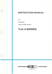
INSTRUCTION
MANUAL
TYPE 1309-A
OSCILLATOR
Form No. 1309-0100-B
ID 1227
July, 1966
Copyright 1962 by General Radio Company
West Concord, Massachusetts, USA
GENERAL
R A D I 0
COMPANY
WEST CONCORD, MASSACHUSETTS, USA
TABLE
OF
CONTENTS
Section 1. INTRODUCTION.
1.1
1.2
1.3
1.4
Purpose . . .
Description .
Controls and Connectors
Accessories Supplied .
Section 2. INSTALLATION.
2.1 Environment
2.2 Rack Mounting .
2.3 Power Connection.
Section 3. OPERATING PROCEDURE
3.1
3.2
3.3
3.4
3.5
3.6
Normal Operation .
Precise Adjustments
Output Connection .
Characteristics . .
Square-Wave Output
Synchronization Jack
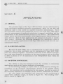
Section 4. APPLICATIONS
4.1
4.2
4.3
4.4
4.5
4.6
4. 7
General . .
Slaved Oscillators
Wave~orm Synthesizer
Accurate Frequency Source with Clean, High, Shortable Output
Tracking, Narrow-Band Filter .
Amplitude-Modulated Oscillator
Output Sync . . . . . .
Section 5. PRINCIPLES OF OPERATION
5.1
5.2
5.3
5.4
5.5
General . • . . . . . .
The Wien Bridge Oscillator
The Oscillator Amplifier .
The Square-Wave Generating Circuit .
The Power Supply . • . . .
Section 6. SERVICE AND MAINTENANCE
6.1
6.2
6.3
6.4
6.5
6.6
6. 7
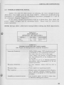
PARTS LIST.
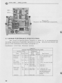
APPENDIX .
Warranty • . . . . • . .
Service . • . • . . . . .
Access to Components • .
Minimum Performance Specifications.
Trouble-Shooting Notes . . .
Amplifier Open-Loop Testing
Calibration Procedure
1
1
1
1
3
4
4
4
6
7
7
7
8
10
12
14
20
20
20
20
21
23
25
26
27
27
27
28
29
30
31
31
31
31
32
33
34
35
43-44
47
SPECIFICATIONS
FREQUENCY
Range: 10Hz to 100kHz in four decade ranges.
Control: Continuously adjustable main dial
covers range in 1 turn, vernier in 4>4' turns.
Accuracy: ±2%.
Synchronization: An external reference signal
can be introduced through phone jack to phaselock oscillator. One-volt input provides ± 3%
locking range. Frequency dial can be used for
phase adjustment.
OUTPUT
Sine Wove
Power: 10 m W into 600- fl load.
Voltage: 5.0
V ±5% open circuit after warmup.
Impedance: 600 fl. One terminal grounded.
Synchronization: High-impedance (12 kn), constant amplitude output of approximately 1.5
volts for use with external counter, for triggering an oscilloscope, or for synchronizing other
oscillators.
Squore Wove
Voltage: Greater than +5 V, peak-to-peak,
open-circuit. De-coupled output.
Impedance: 600 fl.
Rise Time: Under 100 ns into 50 n. Typically
40 ns at full output.
Control: Minimum of 20 dB continuously
adjustable attenuator only.
Sym.;.etry: ±2% over whole frequency range.
GENERAL
Terminals: Two Type 938 Binding Posts, one
grounded.
Control: Minimum of 20-dB,. continuously ad-
justable and 60-dB step attenuator (20 ± 0.2
dB per step). Also, a zero-volts output position
with 600-n output impedance maintained.
Distortion: Less than 0.05% from 200 Hz to
10kHz, increasing to less than 0.25% at 10 Hz
and 100kHz open circuit or 600 n.
~ Frequency Characteristic:
±2% over whole
frequency range for loads of 600 n or greater.
Hum: Less than 50 !J. V regardless of attenuator
setting. (0.001% of full output.)
Accessories
Type CAP-22 Power
Supplied:
Cord, spare fuses.
Accessories Available: Type 1560-P95 Adaptor
Cable (telephone plug to Type 274-M Double
Plug) for connection to synchronizing jack,
relay-rack adaptor set.
Power Required: 100 to 125 V, 200 to 250 V,
50 to 400Hz, 6 W.
Mounting: Convertible-bench cabinet.
Dimensions: Width 8>4', height 6, depth 8Ys
inches (210 by 155 by 210 mm), over-all.
Net Weight: 6%: lb (3.1 kg).
0.3
0.
2~
0
:I:
I-
~o. I " '......
/
""
~
~
~""-'-
0
lOHz
20
50
~
SPECIFICATION
t--o-
PPICALl
100
200
500
I kHz
FREQUENCY
2
1/
5
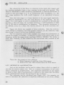
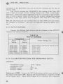
Typical harmonic distortion vs frequency of
Type 1309 sine-wave output.
10
v
/
~
20
v
50
J
100
lt.109-5)
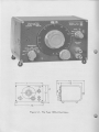
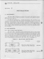
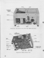
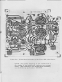
Figure 1-1. The T ype 1309-A Osed
. Ia tor.
INTRODUCTION
SECTION
1
INTRODUCTION
1.1 PURPOSE.
The Type 1309 Oscillator is a general-purpose source of sine and square
waves for laboratory or production use. It features a wide audio frequency
range; an accurate output attenuator; low distortion, hum, and noise; high
stability and accuracy; rapid-transition, highly symmetrical square waves;
plus a synchronizing feature which allows such varied uses as filtering, leveling, frequency multiplying, jitter reducing, and slaving.
1.2 DESCRIPTION.
The all-solid state Type 1309 consists of a Wien bridge oscillator, a
square-wave generating circuit, a constant-impedance (600 ohms) step attenuator, and a power supply.
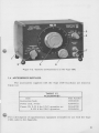
1.3 CONTROLS AND CONNECTORS.
The controls and connectors on the Type 1309 Oscillator are listed in
Table 1-1.
1
~
TYPE 1309
OSCILLATOR
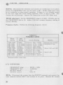
TABLE 1-1
COHTROLSAHDCOHHECTORS
Reference
(Figure 1-2)
2
Name
Type
Function
1
EXT SYNC
Input/ output telephone
jack.
For introducing a syn·
chronizing or ph'\lse·locking
signal from an external
source or for providing
a synchronizing signal,
independent of the output
level, to an oscilloscope,
counter, or another
oscillator.
2
FREQUENCY
Five-position rotary
switch.
3
FREQUENCY
Continuously adjustable
dial.
Combination power switch
and frequency range
switch.
Used with FREQUENCY
range switch to set out·
put frequency.
4
FREQUENCY
Continuously adjustable
vernier.
5
Six-position rotary
OUTPUT
(larger conswitch.
centric switch)
6
OUTPUT
(smaller concentric control)
Continuous rotary
control.
A constant-impedance
bridged-T attenuator
which sets output level
over a 20-dB range
between the steps
selected by the OUTPUT
switch.
7
OUTPUT
600 D
U-inch-spaced binding
post pair.
Lower terminal grounded
to ·chassis. (Refer to
paragraph 3.3 for information on ungrounded
operation.)
(Not
shown)
Power input
(on rear
panel)
Three-terminal male
connector.
For connection to power
line.
(:Not
shown)
LINE
switch
Slide switch.
Selects transformer connections for input voltages
as indicated by the associated legend.
Fine frequency control
(4:25:1) for FREQUENCY
dial.
A 60-dB (20 dB per step)
step attenuator and output signal selector. "OV"
position removes oscillator
output but maintains 600
D output impedance for
noise measurements.
5
6
7
Figure 1-2. Controls and Connectors on the Type 1309,
1.4 ACCESSORIES SUPPLIED.
The accessories supplied with the Type 1309 Oscillator are listed in
Table 1-2.
TABLE 1-2
ACCESSORIES
Item
Instruction book
Power cord, 3-wire
Fuses (2), 0.25 A for 115-V operation or:
0.125 A for 230-V operation
Part Number
1309-0100
4200-9622
5330·0700
5330-0450
For a description of supplementary equipment available for use with the Type
1309, refer to the Appendix.
3
~ TYPE 1309
OSCILLATOR
2
SECTION
INSTALLA TIO·N
2.1 ENVIRONMENT.
The Type 1309 is designed to operate in locations with ambient temperatures from 0 ° to 50 ° C and to be stored in locations with ambient temperatures from -40 to +70 ° C.
As with all low-frequency, variable-capacitance, RC oscillators, the
oscillator circuit in the Type 1309 operates at impedance levels of over 1000
megohms. Consequently, circuit operation, especially frequency accuracy on
the lower ranges, may be affected under conditions of very high humidity.
These effects may be minimized by allowing the instrument a warmup period
long enough to allow internally generated heat to reduce the humidity within
the instrument.
2.2 RACK MOUNTING.
2.2.1 RELAY-RACK ADAPTOR SETS.
The Type 1309
Oscillator can be rack-mounted, alone or with another
8- by 5:4-inch convertible-bench instrument, by means of the appropriate adaptor set listed below. The adaptor panels are finished in charcoal-gray crackle
paint to match the front panel of the instrument and come complete with the
necessary hardware to mount to the instruments and to the rack. For instructions on grounding the rack-mounted Type 1309, refer to paragraph 3.3.
TABLE 2-1. RELAY-RACK ADAPTOR SETS
Type
Description
Catalog
Number
19"
e·x
0
5-1/4"
CONVERTIBLE·
BENCH
INSTRUMENT
0
0
0
Relay Rack Adaptor Set used to
rackmol!nt the Type 1309 alone.
0480-9638
Relay Rack Adaptor Set used to
rackmount the Type 1309 with a
Type 1232, 1311, or 1396.
0480-9636
19"
0
0
e"x
e"x 5-114"
5-114"
CONVERTIBLEBENCH
INSTRUMENT
CONVERTIBLEBENCH
INSTRUMENT
16"
4
0
0
INSTALLATION
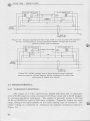
2.2.2 ATTACHMENT OF ADAPTOR SETS. (Figure 2-1).
a. Remove the rubber feet, if
necessary, to clear an instrument mounted below.
b. Remove the screws that secure the front panel to the
aluminum end frames.
c. Remove the spacers between
the front panel and the end
frames.
If two instruments are to be
mounted side-by-side, join them
as follows:
d. On one instrument, install
clips with the front-panel
screws removed earlier and
install the nut plates with
the foot screws removed
earlier.
e. Secure the two instruments
together
with
front-panel
screws through the remaining
hole in each clip and with a
foot screw through the remaining hole in the nut plate.
Note that the instruments can be
bench-mounted side-by-side tn
this manner:
Simply do not remove the two
feet from each outside end frame
and do not install the adaptor
plates.
f. Install two clips on each adaptor plate with the wing
screws, lockwashers, and nuts
supplied.
g. Attach the adaptor plates to
the instrument with the frontpanel screws removed earlier.
h. Mount the assembly in the
rack with the 10-32 screws
supplied.
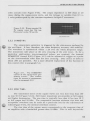
Figure 2-1. Rack mounting the Type 1309 Oscillator.
5
~TYPE 1309
OSCILLATOR
2..3 POWER CONNECTION.
Connect the Type 1309 to a source of ac power as follows :
a. Switch the LINE switch (on the back panel) to the voltage of the power
line (100-125 V or 200-250 V).
b. Connect the oscillator to the line via the 3-wire power cord supplied. The
third wire of the power cord grounds the instrument frame.
The power requirement of the Type 1309 is 6 watts. For a discussion
of the power connection of the instrument as it affects hum, refer to paragraph
3. 3.
6
OPERATING PROCEDURE
SECTION
3
OPERATING
PROCEDURE
3.1 NORMAL OPERATION.
To use the Type 1309 Oscillator as a source of internally generated
sine or square waves :
a. Set the FREQUENCY range switch to the desired frequency range and the
FREQUENCY dial to the de sired frequency.
b. Selection of the output signal:
(1) For sine-wave outp ut, set the OUTPUT switch to one of the center
four positions (the number corresponding to a position indicates the
maximum voltage attainable at that position) , and adjust the OUTPUT
control for the exact voltage required.
(2) For square-wave output, set the OUTPUT switch in the fully clockwise position and adjust the OUTPUT control for the voltage required.
(3) For no output with 600-ohms output impedance maintained, set the
OUTPUT switch in the OV position. This position enable s the operator to avoid the transients associated with turning the o s cillator on
and off and makes zero output possible with no disturbance of the
OUTPUT control.
3.2 PRECISE ADJUSTMENTS.
3.2.1 FREQUENCY.
To set the frequency of the Type 1309 with an accuracy better than the
± 2% accuracy obtainable with the FREQUENCY dial, use of a frequency
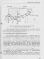
counter such as the General Radio Type 1150 Digital Frequency Meter is recommended. The interconnections for operating the Type 1309 with the Type
1150 are shown in Figure 3-1.
3.2.2 VOLTAGE.
To set accurately the output voltage between the calibrated steps of
the OUTPUT attenuator, use of a voltmeter such as the General Radio Type
1806 Electronic Voltmeter is recommended. The interconnections for operating the Type 1309 with the Type 1806 are shown in Figure 3-1.
7
~ TYPE 1309
OSCILLATOR
TYPE 1560-P95 TELEPHONE
PLUG TO DOUBLE-PLUG PATCH CORD
TYPE 1806
ELECTRONIC
VOLTMETER
.=--------,/
TYPE 1309
OSCILLATOR
Figure 3-1.
Interconnections for operating the Type 1309
with ouxi I iary instruments.
3.3 OUTPUT CONNECTION.
The full oscillator output is available through the front·panel OUTPUT
terminals. The lower terminal, although insulated from the panel at the bind·
.ing post, is internally connected to the circuit ground of the oscillator which
is in turn connected to the chassis. The chassis is normally connected to
the power line ground through the 3-wire power cord.
Hum and extraneous signal pickup due to ground loops may occur when
the oscillator is used with other ac·line-operated equipment. These signals
can be of considerable magnitude compared to the low levels available from
the oscillator's attenuator.
Figure 3-2 shows a ground loop that is formed when the 1309 is bench
mounted with another line-operated device and both use 3-wire power line
connections. If there is 60-Hz ground current flowing through both sides of
the loop, it can cause a voltage drop in the signal lead ground which appears
in the input of the device under test.
c-- J i f P U T
I
~
60-Hz-GROU NO
CURR ENT
t-
1
-
DEVICE UNDER TEST
T
lll~
INPUT
'--v------'
*
1
~
~
r-.
~
1309-12
V3-WIRE AC
POWER LINE
Figure 3-2.
8
A Ground loop. (*60-Hz voltage due to ground current
and signal wire shield resistance).
OPERATING PROCEDURE
When the Type 1309 is used as a bench instrument, the current can usually be sufficiently reduced by operating one of the devices on a two-wire
power cord (see Figure 3-3), which opens the loop.
-
uli[~UT
l
HzGROU NO
60·
NOw_
LOOP
DEVICE UNDER TEST
1
l
lll~
INPUT
'-----v------'
I
*
.,;,.
r"\
-
CURR ENT
1(.3 WIRE
AC
POWER LINE
1309-1
Figure 3-3. Operating the Type 1309-A with a two-wire power cord to eliminate
the ground loop of Figure 3- 2. (*No 60-Hz voltage since ground current
does not flow through signal wire shield).
The "OV" poslt!on on the OUTPUT switch of the Type 1309 can be
very useful in trying to reduce the effects of ground loops. Only the extraneous noise and hum appear at the device input when the oscillator is used in
this position. The oscillator signal is removed, yet all of the wiring, shielding, and impedance levels connecting the two devices remain the same. The
extraneous signals present are much easier to identify and measure in this
case, since they .are not masked by the oscillator output.
If the Type 1309 is rack mounted, the chassis will be connected to the
rack frame ground and a ground loop can not be avoided by operating the instrument with . a two-wire power connection. Again, this loop may cause an
appreciable amount of hum at low levels if there are 60-Hz ground currents
through .the rack panels (Figure 3-4).
The effect of the ground currents may be reduced by isolation of the
oscillator circuit ground from its chassis (Figure 3-5). As much as 10 ohms
may be inserted to provide this isolation. A one-half watt resistor may be
added by replacing the wire lead between AT101 and the front panel ground
connection (see Figures 6-3 and 6-5) or by substit.u ting the connecting wire
link leading to AT101 on top of the printed circuit board. Paragraph 6.3 explains how to obtain access to the top of the board.
9
~ TYPE 1309
OSCILLATOR
DEVICE UNDER TEST
r--
JJfPuT
It-
~
---
1
lll~
INPUT
U-
~
~
'--r------1
*
t---
60-Hz
GROU NO
CURR ENT
T
~
n
-
I
1309·1
lj3-WIRE AC
POWER LINE
Figure 3-4. Ground loop formed when Type 1309 is rock mounted with another
device, not necessarily ac-line operated (*60-Hz voltage due to panel
ground currents and resistance).
TYPE 1309 OSCILLATOR
-
DEVICE UNDER TEST
Ull[~uT 1
~ R!SIOSl
~
-
T
INPUT
lilt
l
~
'--r------1
*
(\
60-H z GROU NO
CURR ENT
--
I
If
3 - WIRE AC
POWER LINE
1309-1.5
Figure 3-5. 60 Hz voltage due to panel ground current reduced
because mast of voltage appears across resistance R rather than
resistance of signal wire shield.
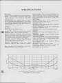
3.4 CHARACTERISTICS.
3.4.1 FREQUENCY RESPONSE.
The output is 5 volts, open-circuit, behind 600 ohms and is adjustable
over a 60-dB range by a step attenuator (20 dB per step) and a 20-dB bridgedT constant-impedance attenuator. The output is constant within ± 2% from
10Hz to 100kHz for loads of 600 ohms or higher. Typically, within the audio
range, changes are imperceptible on the usual analog type of voltmeter. The
output voltage as a function of frequency of a typical oscillator is shown in
Figure 3-6.
10
OPERATING PROCEDURE
~·~,~t I
10Hz
Ill Ill Ill
20
50
100
200
500
I kHz
FREQUENCY
2
5
10
20
1~1
50
100
lm• -,.1
Figure 3-6. Typical oscillator output voltage versus frequency.
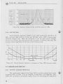
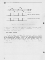
3.4.2 FREQUENCY STABILITY.
High-stability frequency-determining components in the oscillator and
low internal power dissipation result in a stable output frequency. Drift
during warm-up is typically below 0.1%.
Typical long-term stability after warmup at 1 kHz is shown in Figure
3· 7. This graph was plotted under normal laboratory conditions during the
winter months (heat on during the day and off at night).
-
IL
I
--
0
......_
-~.
o.o1•1.
5
"""
It I
I I
10
...................
--
1--
15
-20
HOURS
Figure 3-7. Typical long term drift.
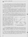
3.4.3 NOISE.
Hum is less than 50J-LV (0.001% of full output), regardless of the attenuator setting. Noise at frequencies distant from a 1-kHz fundamental, measured in a bandwidth of 5 Hz to 500 kHz, is typically 0.005%. Noise close to
the fundamental is also low, as the spectrum analysis of a 1-kHz output shows
(Figure 3·8). Note the absence of components at the line frequency or its
multiples. Refer to paragraph 3.3 for a discussion of how to minimize pickup
of noise from external sources.
11
~TYPE 1309
OSCILLATOR
HORIZONTAL5C:AI..It: I
IN. OIV
10Hz
-120Hz
I Hz
60Hz
I
~ +60Hz ::j:: +120Hz ::::j:::j::::j:
•
I
I
I
Figure 3-8. Spectrum analysis of the oscillator output at 1 kHz.
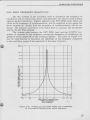
3.4.4 DISTORTION.
Total harmonic distortion (THD) is less than 0.05% from 200 Hz to 10
kHz, and less than 0. 25% at 10 Hz and 100 kHz, with a 600 D load or open
circuited (Figure 3-9). When the attenuator is set for open circuit voltages
of one volt or less, the load seen by the oscillator is between 600 ohms and
an open circuit regardless of the size of the external load.
0.3
0.2
~
0
J:
I-
~a.
I~.....
/
~
""'
"'
i---1
0
lOHz
20
50
"'
r---..
100
200
/
SPECIFICATION
1YPICAL
500
I kHz
FREQUENCY
2
5
10
v
/
-~
20
/
50
J
100
!t.J09-!J!
Figure 3-9. Typical harmonic distortion vs frequency of Type 1309 sine-wave output.
3.5 SQUARE-WAVE OUTPUT.
3.5.1 OUTPUT CHARACTERISTICS.
The square-wave output of the Type 1309 is positive-going from 0 volts
to greater than +5 volts. It is de coupled, so that there is no ramp-off . . This
makes the oscillator a convenient signal source for measuring the ramp-off of
12
OPERATING PROCEDURE
other circuits (see Figure 3-10). The output impedance is 600 ohms at all
times during the square-wave cycle, and the voltage is variable from 0.5 to
5 volts peak-to-:peak by the constant-impedance bridged-T attenuator.
Figure 3-10. Direct-coupled 10Hz square wave has flat top.
Horizontal scale: 50 ms/ div
(d) 10 ms/cm
3.5.2 SYMMETRY.
The square-wave generator is triggered by the sine-waves produced by
the oscillator. It has, therefore, the same frequency accuracy and stability.
The waveform is symmetrical within ± 2% over the whole frequency range.
The transitions take place at the zero crossing of the sine wave. If, for a
particular application, non-symmetrical pulses are required, the internal
SYMMETRY contro.l R303 (Figure 3-11) can be adjusted to trigger on a point
on the sine-waveform other than the zero crossing. Duty ratios of down to
about 20% are possible. For a more detailed explanation of the function of
this control refer to paragraph 5.4.
Figure 3-11.
The SYMMETRY
control of the square-wave gen·
erating circuit.
(For instruc·
tions on access to components,
refer to paragraph 6-3.)
R303
3.5.3 RISE TIME,
The transitions times of the square waves are very fast-less than 100
ns into 50 D (Figure 3-12a). Still faster transitions are possible at full output
and higher frequencies. The rise time is typically less than 4 0 ns into 50 D
at fuU output and 10 kHz. The compromise between minimum rise time and
acceptable overshoot may be made for a particular load by the adjustment of
C302 (Figure 3-13), the internal overshoot control.
The rise time of the square waves corresponds to the response time of
an amplifier with a bandwidth greater than 10 MHz. This is well beyond the
13
~TYPE 1309
OSCILLATOR
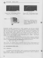
( a) 50 ns/cm·
Figure 3-12a. Leading edge of 10kHz
square wave into SO-D load.
( b) 200 ns/cm
Figure 3-12b. Leading edge of same
signal at open circuited end of cable.
Figure 3-13.
Overshoot control
in the square-wave generating
circuit.
(For instructions on
access to components, refer to
paragraph 6-3 . )
bandwidth normally encountered in audio equipment, but the fast internal
transition can nevertheless be used to advantage for lower frequency testing.
The rise time can be externally lengthened by using the time constant ("-'2.2
RC) of the 600-ohm output impedance and the capacitance ("-'30pF / foot) of
the shielded cable used to cQnnect the oscillator to the device under test.
This produces a monotonically increasing leading edge with no overshoot or
ripple and yet fast enough to check bandwidth up to 1 MHz.
See Figure
3-12b for an example of this waveform.
A wide bandwidth indicator system must be used to reproduce faithfully
the transitions of the square waves. For a system with n individual components of specified rise time, the equation for over-all rise time is
2
2
2
2
T =j T +T +T + · · · · T
r
1
2
3
n •
This means, for example, that a transition time of 50 ns would appear as a
transition time of 70 ns if displayed on an oscilloscope with a 50 ns rise time.
3.6 SYNCHRONIZATION JACK.
3.6.1 GENERAL.
A telephone jack (EXT SYNC, J 103) is located on the left-hand side of
the oscillator. This is an input/ output connector and is used to connect a
signal to the oscillator or to take one from it.
14
OPERATING PROCEDURE
There are three important characteristics associated with the use of the EXT
SYNC feature:
I. Output characteristic.
2. Input synchronizing or phase•locking characteristic.
3. Input frequency-selectivity or filtering characteristic.
~12
3.6.2 OUTPUT CHARACTERISTIC.
EXT SYNC
kil
r------"Mr--;-1-{Q --~
SHIELDED LEADS
I
1
I
OR
_l/COAXIAL CABLE
"'3pF/~~
n ' "'30 pF PER FOOT
I
I
I
jI
A nominal 1.5-volt, rms, output
signal, behind 12 kD, is available
from the EXT SYNC jack. The level
Figure 3-14. Diagram of the EXT SYNC
of this sync output signal is indeoutput equivalent circuit.
pendent of the LEVEL control or the
front-panel OUTPUT load. One side of the sync output is grounded, as shown
in Figure 3-14, and the signal is in phase with the front-panel OUTPUT.
The sync output will drive any size load without increasing oscillator
distortion. However, only high-impedance loads are recommended where full
frequency accuracy is required. The worst-case load, a short circuit, will
decrease the frequency 1 or 2%.
Stray capacitance of most shielded leads or coaxial cables is about
30 pF per foot which, at 100 kHz, amounts to a shunt impedance of about 55
kD. For example, the open-circuited output voltage at the end of a five-foot
shielded lead is less than one volt at 100 kHz. Therefore, cable length should
be kept to a minimum when a high-impedance load is r.o be driven at high frequencies.
L __ _ _
_,_~
___
3.6.3 INPUT SYNCHRONIZING CHARACTERISTIC.
The oscillator frequency may
be synchronized or locked with any
input signal which is applied to the
EXT SYNC jack, if the oscillator
is tuned to the approximate frequency of the input. The range of frequencies over which this synchronization will take place is a function of the amplitude of the frequency component to which the oscillator locks. It increases approximately linearly, and produces a lock
range of about ±3% for each volt
input (see Figure 3-15).
0
3. 4
5
6
7
VOLTS,rms
INPUT AT SYNCHRONIZ lNG FREQUENCY
Figure 3-15.
imo-17!
Locking range versus input voltage.
15
~ TYPE 1309
OSCILLATOR
The oscillator maintains synchronization within the lock range if either
the oscillator dial frequency or the synchronizing frequency is changed. However, there is a time constant of about one second associated with the syncconization mechanism. Thus if the amplitude or frequency of the sync signal
or the dial setting of the oscillator is changed, there will be transient changes
in amplitude and phase for a few seconds before the oscillator returns to ·
steady-state synchronization.
This time constant is caused by the thermistor amplitude regulator as
it readjusts to the different operating conditions. The thermistor is sensitive
only to changes in average values of frequency or amplitude where the averaging time is in the order of seconds. Hence, frequency-modulated and amplitude-modulated sync signals, which have a constant average value of frequency and amplitude over a period of a second or less, are not affected by
this time constant.
For slow changes in frequency or amplitude, the lock range and the
capture range are the same; i.e., the frequency or amplitude at which the oscillator goes from the synchronized state to the unsynchronized state is the
same as when it goes from the unsynchronized state to the synchronized state.
Synchronization is truly phase locking, that is, it maintains a constant
phase difference between the sync
input and the oscillator output. The
phase difference is 0 ° when the
dial frequency is identical to the
sync frequency and approaches :±90 °
as the frequency approaches the
limits of the locking range. Note
that the phase difference is also a
function of the amplitude of the sync
signal because the lock range is a
function of the amplitude (see Figure 3-16).
LOWER LIMIT
OF
DIAL
FREQUENCY
LOCK RANGE
UPPER LIMIT
OF
LOCK RANGE
INPUT FREQUENCY
!1.J1o-1.. j
Figure 3-16. Phase shift relative to input
frequency (and amp I itude).
The input impedance of the EXT SYNC jack is 12 k.\2 at all frequencies
except the synchronizing frequency. At the synchronizing frequency the impedance, in general, is complex and can vary over a wide range including
negative values because the jack is also a source at the synchronizing frequency.
Since the jack is a simultaneous source and input, care should be taken
to insure the sync output voltage does not interfere with the external sync
drive source. The high output impedance of the EXT SYNC jack makes .it
easy to minimize the sync output signal. For example if the jack is fed from
a 600-ohm source, less than 70 mV will appear across the ·source.
16
OPERATING PROCEDURE
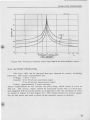
3.6.4 INPUT FREQUENCY SELECTIVITY.
The RC network in the oscillator used to determine the frequency of
oscillation and to reduce hum, noise, and distortion can also be used to filter
signals applied externally. Signals applied to the EXT SYNC jack, which are
close to the frequency of synchronization, will be amplified in the output but
those frequencies distant from the frequency of synchronization will be reduced. The intrinsic selectivity or Q of this filter is constant and determined
only by the RC Wien network.
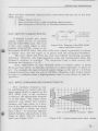
The voltage gain between the EXT SYNC jack and the OUTPUT terminals is constant at any frequency except the frequency of oscillation, regardless of the amplitude of the incoming signals. The curve of Figure 3-17
may be used directly to determine the amplitude of any frequency component
in the oscillator output if the amplitude of the input is known.
200.0
100 .0
70.0
50.0
0
I \
I \
.0
0
IJ
" I-
t-o
0 .7
0.1
-L/
0.2
\
I
0.5
(;.
~
.
~
~
I~
- - - - - - - -__::;
CX)
07
1.0
2.0
5.0
7.0
10.0
FREQUENCY NORMALIZED
INPUT FREQUENCY
DIAL FREQUENCY
Figure 3-17. Voltage gain from EXT SYNC jack ta OUTPUT
as a function of distance from center frequency.
17
~
TYPE 1309
OSCILLATOR
For example. we wish to determine the possible reduction in the harmonic content of a 1-volt, 1-kHz signal which has approximately 1.0% (O.OlV)
second-harmonic distortion by filtering with the Type 1309. The signal is
applied to the EXT SYNC jack, and the OUTPUT control is set for a five-volt
sine-wave output signal. From the graph, the gain at the second harmonic is
approximately 2.2.
distortion, in %
amplitude of harmonics 100 _ 2.2 ;_g.01 x 100 = 0.4 %
4
total amplitude
x
If the amplitude of the external signal is reduced to 0. 5V (0.005-V harmonic content), the distortion at the output of the Type 1309 becomes
(.005)(2.2)
5
X
100 = 0.22%
s1nce the total output voltage and the gain at the second harmonic remain the
same.
In general, it is not possible to reduce the distortion below the level
normally present in the .oscillator and little would be gained in the preceding
example by reducing the input to less than 0.05 volts.
Often the amplitude of a frequency component relative to the. amplitude
of the frequency of oscillation is of greater interest than the--absolute amplitude. Figure 3-18 shows this response for three different input amplitudes.
Notice that the apparent selectivity or Q in this relative response is a function
of the input amplitude. This is because the output at the frequency of oscillation remains constant while the output at other frequencies varies with the
input amplitude.
3.6.5 SYNCHRONIZATION OF SQUARE-WAVE OUTPUT WITH EXTERNAL
SIGNAL.
The square waves produced by the Type 1309 can be synchronized to
an external signal in the same manner as can sine waves. The internal oscillator locks on to the signal at the EXT SYNC terminals in the manner described above, and the resulting sine wave triggers the square-wave generator
to produce a synchronized signal. Thus a synchronous output signal whose
shape and amplitude is independent of the shape of the input signal is generated. This characteristic will prove useful .In, for instance, the generation of
harmonics of the original signal.
18
OPERATING PR.OCEDURE
I~ 'IJO f ~t t
0
-10
-20
A
Ill
""-30
~
J
D.
/
~
\\
1/ 1\\~
vv /
5-40
~
~~
./
-50
~
-60
INPUTS
.........
0 .2 y
~
0 .1 y
0 .05Y
-70
0 .1
0 .2
0 .5
0 .7
1.0
2 .0
5.0
7.0
10.0
FREQUENCY NORMALIZED
(INPUT FREQUENCY)
\ DIAL FREQUENCY
Figure 3-18.
Frequency response of the Type 1309-A for three different inputs.
3.6.6 BATTERY OPERATION.
The Type 1309 can be operated from any external de source, including
batteries. The source requirements are:
Voltage: + 38 to +52 V
Current: 50 to 55 rnA for sine-wave output
55 to 60 rnA for square-wave output
Power: approximately 2 watts minimum
These requirements do not include the pilot lamp, which needs 6 volts at
200 rnA. The source , which should be externally fused with a 1/ 16-A fuse
and equipped with an on-off switch, is connected to the two terminals of C501
as shown in Figure 6-3 and Figure 6-5. The normal internal ac power supply
may be left intact and used in place of the external source as desired.
19
~
TYPE 1309
SECTION
OSCILLATOR·
4
APPLICATIONS
4.1 GENERAL.
The constant output of the Type 1309 Oscillator over its wide frequency
range facilitates frequency-response measurements, while its low hum and
distortion make it very useful for amplifier distortion measurement·s. Since
the noise levels close to the fundamental are low, use of the Type 1309 makes
easy the measurement of amplitude modulation in magnetic recordings and the
measurement of the intermodulation products in any device. The square-wave
output allows the direct measurement of the high-frequency characteristics of
many devices. Most of these applications are common to any sine or squarewave sourc.e . However, the following paragraphs list specifically some of
the more interesting applications of the Type 1309 which result from the synchronization feature.
4.2 SLAVED OSCILLATORS.
Because the EXT SYNC jack is simultaneously an input and an output
connector, two or more oscillators can be synchronized if their EXT SYNC
jacks are connected together. Oscillators connected in this manner will operate at the same frequency or multiples of the same frequency and can be made
to differ in phase (± 75 °) by adjustment of the FREQUENCY dials within the
lock range.
4.3 WAVEFORM SYNTHESIZER.
The ability to lock onto harmonics lends the oscillator to interesting
applications such as the Fourier synthesis of waveforms.
In the following example, a square wave is synthesized by locking the
oscillators on the sucessive odd harmonics present in the original square
wave. Any waveform can be synthesized in this manner, provided a source of
the necessary harmonics is available and the Fourier coefficients are known.
All sync inputs are paralleled and connected to the oscilloscope's
square-wave calibrator output, as shown in Figure 4-1. The resulting waveform is shown in Figure 4-2.
20
APPLICATIONS
TYPE 1560-P95 TELEPHONE PLUG TO DOUBLE-PLUG PATCH CORD (5)
~
OSCILLOSCOPE
Figure 4-1. Set-up for generating the Fourier synthesis of a square wave.
Figure 4-2a. Original 1-kHz square wave
from osc i llascope.
---
a
____.
------
----
------
Figure 4-2b. Fifth harmonic which, like
the output of all the oscillators, is sinusoidal.
Figure 4-2c.
Synthesized square wave.
The five outputs are adjusted for phase
coherence and are summed in the ratio of
their respective Fourier coefficients.
4.4 ACCURATE FREQUENCY SOURCE WITH CLEAN, HIGH, SHORT ABLE
OUTPUT.
One obvious application for the sync capability is to lock one or more
oscillators to a reference frequency for higher accuracy and greater long-term
stability. With the oscillator synchronized, its accuracy and long-term sta·
bility will be identical with the reference; short-term stability or jitter will be
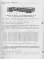
the same as if the oscillator were free-running. (See Figure 4-3 .)
A Type 1309 is locked to the output of a Type 1161-A7C Coherent Decade Frequency Synthesizer, used here as the reference-frequency source.
The oscillator increases the 2-volt output of the synthesizer and reduces the
already low harmonic content for a precision frequency-modulation experiment.
21
~ TYPE 1309
OSCILLATOR
Figure 4-3. The Type 1309
Oscillator being synchronized with the
Type 1161-A7C Coherent Decade Frequency Synthesizer.
The frequency of 31.063 kHz, when used to modulate an fm generator, produces a null in the carrier for a ± 75.000-kHz frequency deviation.
The advantages of this arrangement accrue from the output characteristics of the oscillator listed in the following paragraphs.
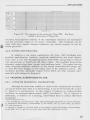
4.4.1 DISTORTION AND HUM REDUCTION.
The frequency selectivity of the synchronized oscillator reduces distortion and hum in the reference source.
For example, Figure 4·4 below is the spectrum of a typical 1-kHz, sinusodial, frequency reference signal, derived by division from a crystal oscillator.
FREQUENCY 1N Hz
Figure 4-4. The spectrum of a typical 1 kHz reference frequency signal.
Figure 4-5 is the spectrum of the output of a Type 1309 Oscillator synchronized to the 1-kHz frequency of Figure 4-4. Note the significant reduction
in distortion, noise, and hum.
4.4.2 FREQUENCY MULTIPLICATION.
The harmonic content of the reference can be used for precise frequency
multiplication since the oscillator can be synchronized to the harmonics. The
22
APPLICATIONS
FREQUENCY IN Hz
Figure 4-5. The spectrum of the output of a Type 1309
locked to the source of Figure 3-4.
Oscillator
accuracy and long-term stability of the submultiple reference are maintained
and the oscillator output is, of course, sinusoidal. This technique can be
used with most signals because harmonics are usually present or can be
easily generated.
4.4.3 OTHER CONTRIBUTIONS.
In addition to the above capabilities, the Type 1309 Oscilbitor also
provides amplification, isolation, amplitude stabilization, and level control.
Less than a volt into the high-impedance EXT SYNC jack produces a full 5volt open-circuit, or 10-mW into 600 ohms, output. The oscillator protects the
reference source from short circuits and nonlinear loads. The output has the
same long-term amplitude stability as the normal unsynchronized output and
is thus free from changes in the output level of the reference source. The
oscillator provides adjustable output levels which are kept constant automatically with changes in frequency.
4. 5 TRACKING, NARROW-BAND FILTER.
4.5.1 JITTER OR INCIDENTAL FM REDUCTION.
Although the short-term stability or jitter* of the synchronized oscillator
can not be better than when it is free-running, it can be better than the source
to which it is synchronized. In this respect it behaves as a phase-locked
oscillator or automatic-phase-control (APC) oscillator.** Or, to express it
differently, it behaves as a tracking, narrow-band filter to reduce short-term
instability.
*
See D.D.Weiner and B.J .Leon, "The Quasi-Stationary Response of L·inear Systems
to Modulated Waveforms,• Proceedings of the IEEE, Vol 53, June 1965, pp 564 to
575 and references.
* * Harold T. McAleer, "A New Look at the Phase Locked Oscillator," Proceedings
of the IRE, Vol 47, pp 1137 to 1143, June 1959 (GR Reprint No. A-79).
23
+.
TYPE 1309
OSCILLATOR
The selectivity of the filter is a function of the input sync signal, and
the tracking mechanics have a time constant in the order of a second. The
effective bandwidth to small frequency perturbations or small fm deviations is
related to the lock range as it is in conventional APC oscillators; i.e., the
lock range produces the 3-dB cutoff frequency of an eq1,1ivalent low-pass
filter.
Since the lock range is a linear function of the sync-signal amplitude,
the effective bandwidth is also the same function of the amplitude. For example, if a 1-volt signal is used to synchronize the oscillator at 100 kHz and
provides a ±3% lock range, the oscillator will have a 3-dB bandwidth of 3 kHz
(3% of 100 kHz) to perturbations in frequency. Thus frequency deviations in
the 100-kHz source at a 3-kHz rate will be reduced 3 dB in the oscillator output.
Figure 4-6 shows one example of jitter reduction. Note the cycle-tocycle change in frequency has been greatly reduced, yet the relatively longterm change of about 1% has been faithfully tracked.
The low frequency used in this example was chosen for convenience in
making the graphic recordings. A reduction in jitter or fm can be made at any
frequency within the range of the oscillator (10Hz to 100kHz). The ability to
track drift, however, is still limited by the one-second time constant of the
thermistor.
TIME
Figure 4-6. One example of jitter reduction.
a. Output frequency of a drifting, jittery 10- Hz source.
b. Output of the Type 1309 synchronized to the 10-Hz source.
4.5.2 INCIDENTAL A-M REDUCTION.
Just as the oscillator can be used to reduce jitter or fm in a signal, it
can also be used to reduce a-m. This is a natural consequence of the oscillator's similarity to a high-Q filter. The amplitude modulation on any signal
to which a Type 1309 is synchronized is reduced to the extent that the modulation sidebands fall outside the passband of the oscillator.
The reduction can be calculated from Figure 3-18. For example, we
wish to determine the reduction in amplitude modulation of a 0.1-volt , 10-kHz
24
APPLICATIONS
signal which has 10% amplitude modulation at 1 kHz (5% or 0.005 V ini each
sideband).
The signal is applied to the EXT SYNC jack ~f the Type 1309,
the output of the Type 1309 is 5 volts and, from the graph, the gain at 9 kHz
and at 11kHz is 15.7.
a-m, in%_ amplitude of sidebands x 100 _ (15.7 x .005) + (15.7 x .005) x 100
total amplitude
5
= 3 _14%
Figures 4-7a and 4-7b show examples of am reduction •
.....
Figure 4-7. One example of o-m reduction.
__
..-.,.._....··~
'
~------ .......... ~-
-
.. ....... ~.
··~-'
a. 10-kHz signal modulated at 500 Hz and
applied to EXT SYNC jock.
b. Reduction in o·m in the output of the
oscillator locked to the signal above.
4.6 AMPLITUDE-MODULATED OSCILLATOR.
If the oscillator is operated outside of the lock range, the sync signal
will beat with the oscillator frequency and produce an audio-frequency, amplitude-modulated output. The modulation will be approximately sinusoidal for
modulation levels up to about 10%.
This arrangement is not ideal, but it does provide amplitude-modulated
signals in the audio range where normally they are not conveniently obtainable. Modulated outputs of this type can be used to measure the effects of
incidental a-m on other measurements and to provide a modulated source to
reduce meter-friction errors in ac measurements.
Figure 4-8 shows one example of amplitude modulation.
Figure 4-8. 10-kHz output of on oscillator
modulated at 500 Hz by o 9.5-kHz signal
applied to the EXT SYNC jock.
-
-~
- .....__
-
.
--...
-
·-
-
-....
-
-- .,
-
-
...
-~
__ ..-
,.,..
25
~
TYPE 1309
OSCILLATOR
4.7 OUTPUT SYNC.
4.7.1 OSCILLOSCOPE TRIGGER (Figure 4-9).
Since the sync output is independent of the output level, it can be used
to trigger an oscilloscope in applications where the oscillator output is often
varied, thereby eliminating frequent readjustment of the oscilloscope trigger
trigger circuits.
I
0
EXT
SYNC
~
OUTPUT
TYPE 1309
IN
OUT
DEVICE UNDER
TEST
EX~
TRIG
VERTICAL
INPUT
OSCILLOSCOPE
\309-19
Figure 4-9. EXT SYNC signal used to trigger an oscilloscope.
4.7.2 COUNTER TRIGGER (Figure 4-10).
A counter can be driven from the EXT SYNC jack when more precise
adjustment of frequency is desired or when the front-panel output is not sufficient to trigger the counter.
1309-20
Figure 4-10. EXT SYNC signal triggers frequency counter.
26
PRINCIPLES OF OPERATION
SECTION
5
PRINCIPLES
OF
OPERATION
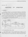
5.1 GENERAL.
As shown 10 Figure 5-1, the Type 1309 Oscillator is a capacitively
tuned Wien bridge oscillator with range changing accomplished in four decade
steps by the changing of RA and RB· A large amount of negative feedback is
used and is responsible for the very low distortion of the sine-wave output.
The 5-volt output of the Wien bridge oscillator is switched either to be
attenuated by a 60-dB step attenuator or (in the 5 V p-p square wave position)
to drive a modified high-speed Schmitt circuit, which generates a very fast
(less than 100-ns rise time) square wave. The square wave is de coupled to
the output through the 0-20-dB adjustable attenuator.
The EXT SYNC jack connects to the negative feedback loop of the Wien
bridge oscillator.
WIEN BRIDGE
01 FFERENTI AL
AMPLIFIER
~~
1309-2A.
Figure 5-1.
Block diagram of the Type 1309-A low distortion oscillator.
5.2 THE WI EN BRIDGE OSCILLATOR.
The oscillator circuit is shown in simplified form in Figure 5-2. The
Wien bridge can be thought of as consisting of two parts: a frequency determining network (CA, CB, RA, and RB), which supplies positive feedback to
sustain oscillation; and a voltage divider (R1 and R2), from which is taken
27
~--T_Y_P_E_1_30_9___o_s_c_IL_L_A_T_O_R________________________________
negative feedback to stabilize the amplitude. The frequency determining network has the following transfer function.
1
where,
f
fo
3 + j (--- - )
f
0
f
At the frequency, f0 , this function equals + 1/3. This frequency is determined
by the ganged variable capacitors CA and CB, and one of four pairs of precision metal-film resistors, RA and RB, selected by the FREQUENCY RANGE
switch.
The resistive divider, R1 and R2, is used to set the gain of the associated amplifier chain that is, the ratio E1/E3, to + 3. The net gain of the
bridge-amplifier loop is then + 1, and the circuit oscillates at the frequency
f0 • The resistance of thermistor R1 adjusts to the value needed to maintain
constant amplitude oscillation. The time constant of the thermistor is short
enough to provide a rapid correction for amplitude variations, but long enough
to cause little distortion at the lower frequencies. (The thermistor operates
at a high temperature in an evacuated bulb, to minimize the effects of ambient
temperature.)
5.3 THE OSCILLATOR AMPLIFIER.
The first stag.e of the oscillator amplifier (shown in simplified form in
Figure 5-2) consists of a field effect transistor, Ql01, connected as a sourcefollower, the drain of which is coupled to the emitter of the following transistor, Q102. This effectively degenerates any gate-to-drain impedance, thereby raising the input impedance.
Q101 is followed by PNP transistor Q102, which serves, in combination
with Q101, as a differential amplifier for Ein> the difference between positive
feedback voltage E1 and negative feedback voltage E2.
The next two stages are NPN transistors: Q103, in common-emitter con·
figuration, and Q104, operating as an emitter-follower.
The oscillator has over 60 dB of negative feedback, which produces
three results: low distortion, very high input impedance and very low output
impedance.
Both the signal output and the positive feedback for the Wien bridge
are taken from the emitter of Ql04. The sine-wave output signal is transmitted through a 600-,u.F coupling capacitor to switch S201, which forms a 60-dB
step attenuator in the first four positions and connects, in the fully clockwise
position, the square-wave generating circuit to the oscillator output_. The
output from the step attenuator is applied to the output jack via a 20-dB, constant-impedance bridged-T attenuator, R205 through R208.
28
PRINCIPLES OF OPERATION
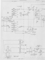
WIEN BRIDGE
AMPLIFIER
AC FEEDBACK
CliO
+Vee
Figure S-2. Simplified schematic diagram of the Wein bridge
oscillator circuit used in the Type 1309-A.
The de operating conditions are maintained by the negative de feedback
divider R108 and Rl09. The proper bias level is set with Rl02. The complete circuit of the oscillator appears in Figure 6-5.
5.4 THE SQUARE-WAVE GENERATING CIRCUIT.
The square-.wave generator (see Figure 6-5) is a modified Schmitt circuit consisting of two emitter-coupled PNP transistors, Q30 1 and Q302. The
circuit works in the following way. An input signal slightly more negative
than the emitter voltage of Q301, applied to the base of Q301, causes it to
turn on (conduct). This forms a positive-going signal at the collector of Q30 1
and the base of Q302. This positive signal causes Q302 to conduct less,
which causes the voltage at the emitter of Q301 to rise. The rising emitter
voltage causes Q301 to conduct all the harder. The result is a regenerative
process which leaves Q301 conducting heavily and Q302 conducting not at
all. When the input signal goes a bit more positive than the voltage on Q30l's
emitter, a similar regenerative process occurs which leaves Q301 off and
Q302 on. The action of the Schmitt circuit is illustrated in Figure 5-3.
Trimmer C302 is a speed-up capacitor which determines how rapidly
Q302 switches on and off, and thereby, the shape of the output waveform,
which appears at the collector of Q302,
For maximum switching speed, Q301 is prevented from saturating by
the network including CR301 and CR302. Diode CR303 prevents the baseemitter voltage of Q301 from becoming excessive d~ing the positive swing of
29
~ TYPE 1309
OSCILLATOR
E
0301 COLLECTOR VOLTAGE
----~~--~----~----~----t
0302 COLLECTOR VOLTAGE
(SQUARE-WAVE OUTPUT)
1309-22
Figure 5-3.
The switching action of the Schmitt circuit.
the input signal. The exact point on the input waveform at which the switch·
ing of Q301 takes place is set by R303, the SYMMETRY control, which ad·
justs the bias at the base of Q301.
5.5 THE POWER SUPPLY.
The power supply, (see Figure 6·5) consists of a full-wave rectifier
(CR501 and CR502) followed by a pi-section filter (R501 and C501, A and B)
and a constant-voltage regulator (Q501). The base voltage of Q501 is held
fixed at + 33 volts by Zener diode CR503; the emitter, therefore, is held at a
fixed voltage. The power transformer T50 1 is wired so that either a 115-volt
or a 225-volt ac power source can be used, depending on the setting of S502,
the LINE switch.
30
SERVICE AND MAINTENANCE
SECTION
6
SERVICE
AND
MAINTENANCE
6.1 WARRANTY.
We warrant that each new instrument manufactured and sold by us is
free from defects in material and workmanship and that, properly used, it will
perform in full accordance with applicable specifications for a period of two
years after original shipment. Any instrument or component that is found with·
in the two-year period not to meet these standards, after examination by our
factory, Sales Engineering Office, or authorized repair agency personnel, will
be repaired or, at our option, replaced without charge, except for tubes or
batteries that have given normal service.
6.2 SERVICE.
The two-year warranty stated above attests the quality of materials and.
workmanship in our products. When difficulties do occur, our service engineers
will assist in any way possible. If the difficulty cannot be eliminated by use
of the following service in's tructions, please write or phone our Service De·
partment (see rear cover), giving full information of the trouble and of steps
taken to remedy it. Be sure to mention the serial and type numbers of the instrument.
Before returning an instrument to General Radio for service, please
write to our Service Department or nearest Sales Engineering Office, requesting a Returned Material Tag. Use of this tag will ensure proper handling and
identification. For instruments not covered by the warranty, a purchase order
should be forwarded to avoid unnecessary delay.
6.3 ACCESS TO COMPONENTS.
To remove the cover of the Type 1309-A, turn the two knurled nuts on
the rear of the cover counterclockwise and pull the cover straight back and off.
To obtain access to the components on the etched board, disconnect
from the etched board the six wires that are connected to the FREQUENCY
range switch, remove the two securing screws, and swing the board up. (See
Figure 6-1.)
31
~TYPE 1309
OSCILLATOR
Figure 6-1.
Access to the etched-board components.
6.4 MINIMUM PERFORMANCE SPECIFICATIONS.
The check of specifications outlined in Table 6-1 is recommended for
incoming inspection or periodic operational testing. Detailed procedures are
given in the Calibration Procedure, paragraph 6. 7.
Conditions: 115-V line, 30-minute warmup.
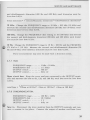
TABLE 6-1
MINIMUM PERFORMANCE SPECIFICATIONS
OUTPUT LEVEL
Check
FREQUENCY
Switch Control
fully
Range
Setting
100Hz-1kHz
5V
Frequency
5V fully cw each
Distortion
5V fully cw 100Hz-1kHz
!kHz-lOkHz
Hum
50mV fully cw 100Hz-1kHz
100Hz-1kHz
Sync output
Output power
5V fully CW lOOHz-1kHz
lOOH z-1kHz
Output re sponse 5V set for
lV, rms 10Hz-100Hz
lOkHz-lOOkHz
Square wave
n_
Rise time
5V fully cw !kHz-lOkHz
p-p fully CW 100Hz-1kHz
Symmetry
Output level
CW
-
OUTPUT
32
fully cw 100Hz-1kHz
Dial
Setting
10
5
2
10
10
10
10
10
I
10
10
10
10
Specifications
5 ±. 25 V ems (open circuit)
±2% of indicated value
< 0.05%
< 0.05%
< 50f.LV
~I.5V
~ 2.45
V inro 6ool1 (10 mW)
0.98-1.02
0.98-1.02
v
v
< 100 ns into son
±2%(48-52% duty ratio)
on scope trace, or less
than 6% 2nd harmonic
component to funda·
mental
~ 5 Vp·p
SERVICE AND MAINTENANCE
6.5 TROUBLE-SHOOTING NOTES.
Tables 6-2 and 6-3 offer means of isolating the more straight-forward
difficulties that might occur in the Type 1309-A. Additional troubleshooting
information is contained in the Calibration Procedure, paragraph 6. 7, and on
the schematic diagram, Figure 6-5.
In all cases, except total failures such as a blown fuse, first check the
power supply voltages and de operating level. These must be correct for
proper operation.
NOTE: Always allow a 30-minute warmup before making any final adjustments.
TABLE 6-2
SPOT CHECK OF
IMPORT ANT VOLT AGE LEVELS
SUPPLY
Power
DC bias
VOLTAGE
+ 32
VDC
+ 18.0 V DC
TEST POINT
Emitter Q50 1
TP A
TABLE6-3
TROUBLE SYMPTOMS AND THEIR CAUSES
(See Figures 6-2 through 6-5 for component locations.)
Inaccurate frequency ............... 10kHz-100kHz range. Cl05 misadjusted, refer
to paragraph 6. 7. 5 for adjustment procedure.
· One range only: Ra or Rb for that range.
Lower ranges: Dirt, grease, or high humidity
may have affected Ra or Rb, frequency will
be too high.
All ranges: Ca or Cb or improper frequency
adjustments, refer to paragraph 6.7.5 for ad·
justment procedure.
Excessive distortion ............... DC bias improper, adjust R102 for +18V at
TP A.
Excessive hum .................... Power supply not regulating properly.
Poor response ... · ................. (-output varies with frequency) R111 (thermistor) or grossly improper frequency adjustments, refer to paragraph 6.7.5 for adjustment
procedure.
Instability or excessive noise ..... Oust between plate~ of C401 or wiper dirty
or otherwise making poor contact.
33
~
TYPE 1309
OSCILLATOR
6.6 AMPLIFIER OPEN-LOOP TESTING.
The amplifier uses a large amount of ac feedback, so that trouble at
any one point in the circuit will manifest itself at most other points. For this
reason it may be difficult to isolate a failure under closed-loop conditions;
therefore the following open-loop test is recommended:
a. Unsolder the lead to AT111 on the etched board and unsolder one
end of the thermistor, Rlll to open the ac feedback path (see Figure 6-4).
b. Set the controls as follows:
FREQUENCY range .... 10kHz- 100kHz
FREQUENCY dial . . . . . 1 (10kHz)
OUTPUT switch . . . 5V
OUTPUT control .... fully cw
c. Apply a 60-mV, p-to-p, 1-kHz signal to the EXT SYNC jack, J401.
d. Trace the signal through the amplifier with an oscilloscope, using a
short, low-capacitance, high-impedance probe to prevent spurious
oscillation.
The voltages observed should agree with those of Table 6-4, and the waveforms should all be sine waves.
TABLE 6-4
OPEN-LOOP VOLTAGES AND WAVEFORMS
IN THE OSCILLATOR AMPLIFIER
Test Point
AT109
ATllO
QlOl, drain and source
Junction of Rl05, Cl03
AT108
Ql02, collector
Ql03, emitter
Ql03, collector
Ql04, emitter
Junction of R115, CliO
ATlll
Yo It age (peak-to-peak)
60mV
30mV
30mV
30mV
30mV
40mV
30mV
14V
14V
14V
14V
Voltages are approximate. Actual voltages may vary
2 to 1 in individual instruments.
34
SERVICE AND MAINTENANCE
6.7 CALIBRATION PROCEDURE.
6.7.1 INTRODUCTION.
This procedure can be used for troubleshooting or calibration.
If used for trouble shooting, the steps can be performed in any order.
The usual practice would be to perform only the step that pertains to the suspected circuit.
If used for calibration, the steps should be performed in sequence since
one step serves as a foundation for the next. A complete calibration insures
that all circuits are operating properly and within specifications. The Type
1309
Oscillator incorporates the high reliability one would expect of conservatively designed, semiconductor circuits and routine calibrations are
unnecessary.
6.7.2 EQUIPMENT.
The following equipment 1s required for a complete calibration of the
Type 1309 Oscillator. The specifications given for the equipment are those
necessary for the calibration of the Type 1309 and are not necessarily those
of the recommended equipment.
Metered, adjustable autotransformer
Output: 105 to 125 V (or 195 to 235 or 210 to 250 V), 12 W.
Meter: Ac, ±3% accuracy.
The Type W5MT3W Metered Variac® Autotransformer is recommended.
Electronic voltmeter
Voltage: 0 - 50 V, de; 5mV - 5 V ac, rms, 10 Hz 100kHz, ±2% accuracy.
Impedance: 100 kD or greater.
·Digital frequency meter (counter)
Frequency: 10 Hz to 100 kHz, ±0.1% accuracy
Sensitivity: 1 V, rms.
Impedance: 100 kD or greater.
The Type 1151 Digital Time and Frequency Meter is recommended.
The frequency accuracy of the Type 1309 is ±2%. The counter accuracy should be at least 20 times this, or 0.1%, to prevent counter errors
from entering into the measurements. The ±one-count uncertainty in a counter
with a 100-kHz time base represents an error of greater than 0.1% unless the
35
~
TYPE 1309
OSCILLATOR
measurement conditions are as follows:
above 1000 Hz; direct frequency measurement, 1-second counting interval.
below 1000Hz; period measurement, 10-period count.
Oscilloscope
Bandwidth: de to 30 MHz ( -3 dB points)
Sensitivity: 50 mV
Impedance: 100 kD or greater.
The Tektronix Type 543/543A Oscilloscope with a Type CA Plug-in and Type
P6000 Probe is recommended.
Wave Analyzer and/or Distortion Meter
Frequency: 10 Hz to 100 kHz.
Sensitivity: 50 j.LV to 5 V
Impedance: 100 kD or greater.
The Type 1900-A Wave Analyzer and the Hewlett Packard Type 334-A Distortion Meter are recommended.
Test Oscillator
Frequency: 1 kHz.
Amplitude: 1 V into 25 kD.
The Types 1309, 1310 and 1311 Oscillators are recommended.
Load resistors
50 D ±1%, 1W. The Type 500-C Resistor is recommended.
600 D ±1%, 1W. The Type 500-G Resistor is recommended.
Cables
Telephone-plug to double plug.
The Type 1560-P95 Cable is recommended.
6.7.3 POWER SUPPLY and BIAS VOLTAGES.
Connect the Type 1309 to an ac line via a metered adjustable autotransformer and set the transformer for 115-V output. Set the Type 1309 controls as follows:
FREQUENCY range . . . . . 100 Hz - 1 kHz
FREQUENCY dial . . . . . . 10 (1kHz)
OUTPUT switch . . . . . . . 5 V
OUTPUT control. . . . . . . fully cw
36
SERVICE AND MAINTENANCE
Power Supply. Connect a voltmeter to the emitter of Q50 1. Voltage should
be 32 ±2 volts de. If not, check CR503 and replace if necessary.
Bias. Connect a voltmeter to TPA and adjust R111 for + 18 V, de.
Ripple. Connect the oscilloscope to the emitter of Q501 and check ripple at
100, 115, and 125-V line; must be less than 10 mV, p-to-p.
Allow a 30-minute warmup then recheck the adjustment of Rlll.
6.7.4 OUTPUT LEVEL.
FREQUENCY range.
FREQUENCY dial . . . .
OUTPUT . . . . . . . . .
OUTPUT control . . . . . . •
100Hz- 1kHz
10 (1 kHz)
5V
fully cw
Maximum output. Connect a voltmeter to the OUTPUT terminal and adjust
R112 for 5 V, rms. The instrument should be on for at least 30 minutes before
this adjustment is made.
OUTPUT control operation. Vary the OUTPUT-control over its full range the
output level must change smoothly. If it does not, the OUTPUT potentiometer, R205, is noisy and should be replaced.
6.7.5 FREQUENCY
FREQUENCY range . . .
1 kHz - 10 kHz
FREQUENCY dial . . . . . . 1 (1kHz)
OUTPUT switch . . . . . . . 5 V
OUTPUT control. . . . .
fully cw
kHz mechanical adjustment. Connect the counter and voltmeter to the EXT
SYNC jack and set the FREQUENCY dial for a frequency count of exactly
1.000 kHz. Loosen the set screws on the FREQUENCY dial and position the
dial on the shaft to read exactly 1 with a reading of 1.000 kHz on the counter.
Snug-up the set screws but don't tighten. Note the voltmeter reading.
10 kHz, capacitor adjustments. Set the FREQUENCY dial to exactly 10.
Simultaneously adjust C402 and C403 for a counter frequency reading of exactly 10 kHz and the same voltmeter reading noted above.
The mechanical adjustment and capacitor adjustments interact: repeat until
the measurements are correct and the voltmeter readings are equai at both
ends of the dial.
37
~ TYPE 1309
OSCILLATOR
Stabi Iity. Disconnect the voltmeter and connect an oscilloscope in its place.
Rotate the FREQUENCY dial over the entire 1 kHz - 10 kHz range; there must
be no instability or other erratic operation. If there is, it is usually caused
by the rotor wiper arm of the tuning capacitor, C40 1, or dust in C401. Disconnect the oscilloscope. Remove all connections to the EXT SYNC jack.
100kHz adjustment. Set the FREQUENCY range to 10kHz- 100kHz and set
the FREQUENCY dial to 10. Adjust C105 for a counter frequency reading of
exactly 100 kHz.
Frequency checks. Perform the following frequency checks:
TABLE 6-5
FREQUENCY CHECK
Range
Setting
Dial
Setting
Counter Reading
Remarks
*1kHz-10kHz
1kHz-10kHz
1kHz-10kHz
1kHz-10kHz
*1kHz-10kHz
100Hz-1kHz
10kHz-100kHz
*10kHz-100kHz
10Hz-100Hz
10Hz-100Hz
1(1kHz)
1. 5( 1. 5kHz)
2.5(2. 5kHz)
5(5kHz)
10(10kHz)
5(500Hz)
5(50kHz)
10(100kHz)
10(100Hz)
1(10Hz)
Frequency: 980 to 1020Hz
Frequency: 1470 to 1530Hz
Frequency: 2450 to 2550Hz
Frequency: 4900·5100Hz
Frequency: 9800-10,200Hz
Ten period 19.6 to 20.4 ms
Frequency: 49 to 51kHz
Frequency: 98.0 to 102kHz
Ten period 98 to 102 ms
Ten period 980 to 1020 ms
*Mechanically position
FREQUENCY dial
*Adjust C402 and C403
*Adjust C105
*Adjusted earlier in this step.
6.7.6 DISTORTION.
FREQUENCY range.
FREQUENCY dial . .
OUTPUT switch. . .
OUTPUT control . . .
.
.
.
.
.
. . .
.
. . .
100Hz- 1kHz
2 (200 Hz)
5V
fully cw
200 Hz. Disconnect the counter from the OUTPUT terminals and connect the
wave analyzer and the 600-D load resistor in its place. Measure the second-
38
SERVICE AND MAINTENANCE
and third-harmonic distortion (400 Hz and 600 Hz); total distortion fllUSt be
less than 0.05%.
Total distortion= ~ (second-harmonic distortion)2 +(third-harmonic distortion)2
10 kHz. Change the FREQUENCY range to 10 kHz - 100 kHz (10 kHz) and
measure the second- and third-harmonic distortion (20 kHz and 30 kHz); total
distortion must be less than 0.05%.
100 kHz. Change the FREQUENCY dial setting to 10 (100 kHz) and measure
the second- and third-harmonic distortion (200 kHz and 300 kHz); total distortion must be less than 0.25%.
10 Hz. Change the FREQUENCY range to 10 Hz- 100 Hz and the FREQUENCY dial to 1 (10 Hz). Measure the second- and third-harmonic distortion (20
Hz and 30Hz); total harmonic distortion must be less than 0.25%.
These measurements may also be made with a distortion meter.
6.7.7 HUM.
FREQUENCY range.
. ..
FREQUENCY dial . . . . . . •
OUTPUT switch . . . . . . . .
OUTPUT control . . . . . . . .
1kHz- 10kHz
1 ( 1 kHz)
500 mV
fully cw
Open circuit hum. Keep the wave analyzer connected to the OUTPUT terminals and measure the hum at 60, 120, and 180 Hz; total hum must be less than
0.01%.
total hum =
~(hum
at 60 Hz)2 +(hum at 120 Hz)2 +(hum at 180 Hz)2
6.7.8 SYNCHRONIZATION.
FREQUENCY range .. .
FREQUENCY dial . . . .
OUTPUT switch . . .
OUTPUT control . . . . .
. 100 Hz - 1 kHz
. 10 (1kHz)
. 5
v
. fully cw
Sync in. Disconnect the wave analyzer from the OUTPUT terminals and connect a counter in its place. Connect the output of another oscillator (test
39
~
TYPE 1309
OSCILLATOR
oscillator) to the EXT SYNC jack and set the test oscillator for IV, rms, of
exactly 1 kHz.
Very slowly incre.a se the FREQUENCY dial setting of the Type 1309
until it drops out of sync (counter reading changes from 1 kHz to some higher
frequency). Reduce the output amplitude of the test oscillator to below 50mV,
rms, or turn its power switch off and note the counter reading (free-running
frequency of the Type 1309); must be greater than 1030 Hz (1 kHz ±3%).
Sync out. Disconnect the test oscillator from the EXT SYNC jack and connect
the voltmeter in its place. The sync out amplitude should be approx 1.5 V
rms.
6.7.9 OUTPUT RESPONSE.
Connect the 60D-ohm load resistor and the voltmeter to the OUTPUT
terminals and check as follows:
TABLE 6-6
OUTPUT RESPONSE
FREQJENCY
Dial
Range
·Setting
Setting
100Hz-1kHz
100Hz-1kHz
100Hz-1kHz
10Hz-100Hz
1kHz-10kHz
10kHz-100kHz
10 (1kHz)
5 (500Hz)
1 (100Hz)
1 (10Hz)
10 (10kHz)
10 (100kHz)
Output Voltage, rms
Set OUTPUT controls for exactly 2.5V
2.55 to 2.4V
2.55 to 2.4V
2.55 to 2.4V
2.55 to 2.4 V
2.55 to 2.4V
6.7.10 CALIBRATION PROCEDURE FOR SQUARE-WAVE OUTPUT.
SYMMETRY.
FREQUENCY range . . . . . .
FREQUENCY dial •••••.•
OUTPUT switch . . . . . . . .
OUTPUT control . • • • . . . .
10 Hz • 100 Hz
10
11J5 V p-p
cw
Adjustment of R503. Connect the 50-D load resistor and the wave analyzer to
the output of the Type 1309. Measure the second harmonic component (2 kHz)
of the square wave. Adjust R503 (Figure 6-3) to minimize this component.
40
SERVICE AND MAINTENANCE
SQUARE-WAVE CHECKS.
Rise time adjustment.
FREQUENCY range •...•. 10 kHz - 100 kHz
FREQUENCY dial . . • • . . . 10
OUTPUT switch . • • . • . . . rlJ 5 V p-p
OUTPUT control . • . . . . . • cw
With the oscilloscope observe the output of the Type 1309 into the 50-D load
resistor. Set the scope controls as follows:
Dual trace operation (MODE) •••.•• one channel only
Volts/div • . . . . . . . . . . . . . . . . • 0.1 V
Time/ div • . . . • . • . . . . . . . . . . . • 10J.Ls
Adjust C302 (Figure 6-3) for minimum overshoot and fastest rise time on the
leading edge. There should be no noticeable ringing.
Measure the rise time of the square wave.
It should be less than 100 J.LS.
Output Amplitude. Remove the 50-D load resistor and measure the unloaded
square-wave output. It should be at least 5 volts peak-to-peak.
Droop.
FREQUENCY range . . • . . . 10 Hz to 100 Hz
FREQUENCY dial ••.••.. 1
Observe the square wave on the oscilloscope. There should be no measurable
droop or ramp-off.
41
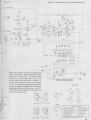
THROUGH
HOLES
C403~
C402---
Figure 6-2. Top interior view of the Type 1309-A Oscillator.
ATill
ATIOI
QIOI
DRAIN
ATI02
TPA
(0104 EMITTER)
AT II
- }CONNECTION
POINTS FOR
BATTERY
+
-JUNCTION
Rll5, CliO
Figure 6-3. Bottom interior view.
42
PARTS
REF NO.
LIST
DESCRIPTION
PART NO.
CAPACITORS
C101
C102
C103
C104
C105
C106
C107
C108
C109A
C109B
CliO
Cll1
C301
C302
C401A,B
C402
C403
C404
C405
C501A
C501B
C502A
C502B
Electrolytic, 151-!F +100-10% 15V
Electrolytic, 151-!F +100-10% 15V
Electrolytic, 151-!F +100-10% 15V
Electrolytic, 10f.!F +100-10% 25V
Trimmer, 5-25pF
Mica, 62pF ±5%
Ceramic, 0.1f.!F 50V
Electrolytic, 200f.!F +100-10% 6V
Electrolytic, 300f.!F y
35
Electrolytic, 300f.!F
Electrolytic, 151-!F +100-10% 15V
Ceramic, 470pF ±10%
Electrolytic, 10f.!F +100-10% 25V
Trimmer, 8-50pF
Variable, Air, 630pF FREQUENCY
Trimmer, 5.5-18pF
Trimmer, 5.5-18pF
Mica, 39pF ±5%
Ceramic, 1.2pF ±5%
Electrolytic, 2001-!F y
50
Electrolytic, 200f.!F
Electrolytic, 300f.!F y
Electrolytic, 3001-!F 35
4450-3700
4450-3700
4450-3700
4450-3800
4910-1150
4700-0364
4403-4100
4450-2610
4450-2400
4450-3700
4404-1478
4450-3800
4910-1170
1210-4000
4910-2041
4910-2041
4640-0200
4400-0120
4450-5591
4450-2400
DIODES
CR301
CR302
CR303
CR501
CR502
CR503
High-speed, Type 1N625
Zener, Type 1N971B
High-speed, Type 1N625
Rectifier, Type 1N3253
Rectifier, Type 1N3253
Zener, Type 1N973B
6082-1012
6083-1049
6082-1012
6081-1001
6081-1001
6083-1036
MISCELLANEOUS
F501
J201
J202
J401
P501
PL501
Q101
Q102
Q103
Q104
Q301
Q302
Q501
S201
S401
S501
S502
T501
FUSE, 0.125A 3AG, Slo-Blo
JACK, Jack-top, binding post, OUTPUT
JACK, Jack-top, binding post, Ground
JACK, Phone jack, two contact, EXT SYNC
PILOT LIGHT, 6V, 200mA
PLUG, 3-terminal, power
TRANSISTOR, Type U-147, field effect
TRANSISTOR, Type 2N3905
TRANSISTOR, Type 2N2714
TRANSISTOR, Type 2N697
TRANSISTOR, Type 2N3905
TRANSISTOR, Type 2N3905
TRANSISTOR, Type 2N697
SWITCH, 6-position rotary, OUTPUT
SWITCH, 6-position rotary, FREQUENCY
SWITCH, power OFF part of S201
SWITCH, slide, LINE
TRANSFORMER, Power
-----
5330-0450
0938-3000
0938-3000
4260-1260
5600-1001
4240-0600
8210-1090
8210-1114
8210-1047
8210-1040
8210-'1114
8210-1114
8210-1040
7890-4210
7890-4200
7910-0831
0745-4380
43
PARTS LIST (con t)
REF NO.
DESCRIPTION
PART NO.
RESISTORS
R101
R102
Composition, 22kQ ±5% 1/2w
.Potentiometer, composition, 25kQ ±20%
(BIAS)
R103
Composition, 10kQ ±5% 1/2w
R104
Composition, 12kQ ±5% 1/2w
R105
Composition, 4 7kQ ±5% 1/2w
R106
Composition, 51kfl ±5% 1/2w
R107
Composition, 27kQ ±5% 1/2w
R108
Composition, 3.3kQ ±5% 1/2w
R109
Composition, 15kQ ±5% 1/2w
RllO
Composition, 5600 ±5% 1/2w
R1ll
Thermistor
Rll2
Potentiometer, composition, 5000 ±20%
Rll3
Composition, 10kQ ±5% 1/2w
Rll4
Composition, 2700 ±5% 1/2w
Rll5
Composition, 5.6kQ ±5% 1/2w
Rll6
Composition, 1kQ ±5% 1/2w
Rll7
Composition, 1000 ±5% 1/2w
Rll8
Composition, 2.4kQ ±5% 1/2w
Rll9
Composition, 5100 ±5% 1/2w
R201
Film, 6650 ±1% 1/2w
R202
Film, 6.65kfl ±1% 1/2w
R203
Film, 66.5kQ ±1% 1/2w
R204
Film, 604k0 +1% l/2w
R205A,B Potentiometer, composition, (OUTPUT
control)
R206
Composition, 6200 ±5% 1/2w
R207
Composition, 6200 ±5% 1/2w
R208
Composition, 360 ±5% 1/2w
R301
Composition, 1.2k0 +5% 1/2w
R302
Composition, 15k0 ±5% 1/2w
R303
Potentiometer, composition, 2.5k0 ±20%
(SYMMETRY)
R304
Composition, 10k0 ±5% 1/2w
R305
Composition, 22k0 ±5% 1/2w
R306
Composition, 6200 ±5% 1/2w
R307
Composition, 2.0k0 ±5% 1/2w
R308
Composition, 1000 ±5% 1/2w
R309
Composition, llkO ±5% 1/2w
R310
Composition, 4. 7k0 ±5% 1/2w
R401
Film, 26.7MO ±1% 1w
Film, 26.7MO ±1% 1w
R402
R403
Film, 2. 67MO ±1% 1/2w
R404
Film, 2.67MO ±1% 1/2w
Film, 267k0 ±1% 1/2w
R405
R406
Film, 267k0 ±1% 1/2w
R407
Film, 26. 7k0 ±1% 1/2w
R408
Film, 26. 7k0 ±1% 1/2w
R501
Composition, 470 ±5% 1w
R502
Composition, 2. 7k0 ±5% 1/2w
44
6100-3225
6040-0800
6100-3105
6100-3125
6100-3475
6100-3515
6100-3275
6100-2335
6100-3155
6100-1565
6741-2023
6040-0300
6100-3105
6100-1275
6100-2565
6100-2105
6100-1105
6100-2245
6100-1515
6450-0665
6450-1665
6450-2665
6450-3604
6045-llOO
6100-1625
6100-1625
6100-0365
6100-2125
6100-3155
6040-0500
6100-3105
6100-3225
6100-1625
6100-2205
6100-ll05
6100-3ll5
6100-2475
6550-5267
6550-5267
6450-4267
6450-4267
6450-3267
6450-3267
6450-2267
6450-2267
6110-0475
6100-2275
T
<@> 1309-0700/ 3
----
~ O_aJ
I .....
-----~.;...
Figure 6-4. Etched-board assembly of the Type 1309-A Oscillator.
NOTE: The number appearing on the etched board is
the number of the board only, without circuit compo·
nents. When ordering a new etched- board assembly,
use the following part number: 1309- 2700.
WIEN B R I D G E - - - - - - - - - - - - - - - - - -
AMPLIFIE.
I
----Ac 8 oc 1
I
I
R408
26.TK
lOOkHz 107F
106F
ZOtiR
R406
267K
~
10kHz
105F
205R
Ro
I kHz
R404
2,67M
5401
f32V
[£JJc
!O<IF
Z04RR402
J401
100Hz
26.7M
20.JRIW
IO.JF
10Hz
Co
OFF
OFF
10Hz
40.JR
100Hz
J04·F~Rv4"'0~3-4o 404R
2.67M
AT!I51j~l0'-7•F- "-'AT'-"/II~O~-----t==~---~-------J~-J
S401
lkH 1
FRAMEj
405R
.J05FR405
5401
•
10kHz
267K
406R
Jor.FR4 07
26.TK
100kHz
•
+IBV
I
I
R/10
560
100 KHz
ADJUST
407R
.JOBR
AT/06
r-----------------~~T501
BK
LINE
100
zoo
125 Z50
50-400Hz
+32V
BK
CR501
F50!
Y£
WH-GN
I
6
I
,~---,
WH-BL
5501
WH-RO
GANG£0 TO RANGE
SWITCH 5401
L
PL501
POWER SUPPLY -
------
I
AMPLIFIE_R------ - - - - - -- - -- - - -- - - - - - - . . .
--l
Figure 6-5.
Schemat ic d iagram of the Type 1309-A Oscillator.
- A C 8 OC FEEDBACK
+32V
, - - - -- - - - - - - SCHMITT CIRCUIT -
R/15
5 . 6K
-
-
I
------,
+32V
CliO
15pF
R308
100
+
I
+32V
+32V
R/16
IK
+32V
;!;'
~-14V p~ t------~
_ ____j__
Cl07
0.1
SY MMETRY CW
I
R305
22K
CR303
@
;~f: ~-----1>-----1H
0/04
---.-
~r""'~-~-'•"'o-.,,.,
+32 V
I
I
0 103
~ ""J/4Vp.p
-,
R/13
!OK
R/14
270
4C/1/I
70
R/17
IJO
I
~~\. . ,.=.,---------+----1
+18V
R
2.
4K / 1 8
. h
+ C/08
1200pF
_j
AT I05
R/19
510
1w
1
20fR
202R
203R
204R
AT 102
~:-------Rotary switch sections are shown as viewed from the
panel end of the shoft. The first digit of the contact
number refers to the section. The section nearest
the panel is 1, the next section back is 2, etc. The
next two digits refer to the contact, Contact 01 i s
the first positi~n clockwise from a strut screw (usually, the screw above the locating key), and the other
contacts are numbered sequentially (02, 03, 04, etc),
proceeding clockwise around the section. A suffix F
or R indicates that the contact is .on the front or rear
of the section, respectively.
vr
,-L-~~~~~~~-~-------~~~-+~
I ~
;_.., ...,.----~
......
AT/20
*R205A,8 PLUS R206,R2078 R208- FORM A
600n CONSTANT IMPEOANCE ATTENUATOR
tiA SE
EM~
;v
5C Mv e
8/AS
I
Vcot.L
0102, 03 01,0302
P· P
GAT£
S201
A
V
oRAIN
S201
0101
SECTI.Jt: 2 REAR
S EC TI ON I FRO!I/T
0 103
FREQUENCY
r.
31/F0tl
~~-- o ~
I
_
0104,05 01
e '5v
I
I
@
BI AS
E
M
A
JcoLL
ru
S OURCE
R/03
/OK
DIAGRAM
(8 0TTVM VIEW)
sao ..;
!--o--J....-+ +32V
J201
'
_j
0
T o
I
J0 2F
""010 l t'•"'-~
...
\ _/ J06 F
S401
SECTION 2 REAR
SECr'(ON 3 FRONT
I KHz
100 11z~~ IO I<Hz
lOHz / .
•
•
OFF~
5 4 01
~ 100
""'
NOTE UNLESS S PECIFIED
1 POSITION OF ROTARY SWITCHES
SHOWN COUNTERCLOCKWISE
5 RESIST ANCE IN OHMS
K 1000 OHM S M 1 MEGOHM
2 'coNTACT NU MBERING OF SWITCHES
EXPLAINED ON SEPARATE SHEET
SUPPLIED IN INSTRUCTION BOOK
6 CAPACITANCE VALUES ONE AND
OVER IN PICOFA RADS. LESS
3 REFER TO SERVICE NOTES IN INSTRUC·
TION BOOK FOR VOLTAGES
APPEARING ON DIAGRAM
7
4 RESISTORS I ·2 WATT
THAN ONE IN MICROFARADS
0
0
AT
10 TP
KNOB CONTROL
SCREWDRIVER CONTROL
ANCHOR TERMINAL
TEST POINT
ANCHOR TERMINALS USEO: AT/01 THRU if58 120
45
APPENDIX
SUPPLEMENTARY EQUIPMENT AVAILABLE.
Type 480-P308 Relay Rack Adaptor Set
This adaptor set allows the oscillator to be
mounted in a standard 19-inch relay-rack.
Type 480-P316 Relay-Rack Adaptor Set
This adaptor set allows the oscillator to be
mounted sid'e·by-side with another 8 x 5~·inch,
convertible-bench instrument in a standard 19inch relay rack.
Type 1396 Tone Burst Generator.
This instrument allows the output of the oscillator to be gated on and off coherently. The
gate-on and gate-off times are independently
adjustable from 2 to 128 cycles of any output
frequency of the oscillator up to 100 kHz.
With the Type 480-P316 Relay-Rack Adaptor
Set, listed above, the Type 1396 and Type
1309-A can be bolted together to form a single
unit for either bench or rack installation.
Type 1232 Tuned Amplifier and Null Detector.
This instrument, with the oscillator, forms a
detector-oscillator assembly with a sensitivity
of 0.1 J.LV and a frequency range of 20 Hz to
20 kHz, plus two fixed frequencies of 50 and
100kHz.
With the Type 480-P316 Relay-Rack Adaptor
Set listed above, the Type 1232 and oscillator
can be bolted together to form a single unit for
either bench or rack installation.
47