1
US006S29727B1
(12)
(54)
United States Patent
(10) Patent N0.:
Pawloski
(45) Date of Patent:
Dec. 7, 2004
IN-CIRCUIT EMULATION OF SINGLE CHIP
6,571,356 B1 *
5/2003 Mehr et al. ................. .. 714/28
MICROCONTROLLERS
6,598,176 B1 *
7/2003 Tago ....... ..
2002/0007264 A1 *
(75)
US 6,829,727 B1
Inventor:
1/2002
714/28
SWoboda
. . 703/28
714/28
Martin B Pawloski, Scottsdale, AZ
2002/0062461 A1 *
5/2002 Nee et al.
(Us)
2002/0099977 A1 *
7/2002 Wong ........................ .. 714/28
* cited by examiner
( 73 )
As'
slgnee :Mtl'kC
eam
Orp .Ch
’
an dl er’ AZUS
( )
(*)
Notice:
Subject to any disclaimer, the term of this
patent is extended or adjusted under 35
Primary Examiner—Robert Beausoliel
Assistant Exammer—YOlanda L Wllson
(57)
ABSTRACT
U.S.C. 154(b) by 329 days.
An in-circuit emulation sy stem consistin g of an emulation
(21) APPL N0: 09/759’577
(22)
Filed:
base and a slightly modi?ed, ?ash-based COPS architecture
m1crocon tllIddttth?h
ro er. n a
1 ion 0
e as memor yhth
W ere
e
Jan. 12, 2001
User’s program resides, the COPS device includes a small
ROM area With a monitor program that is used to commu
7
(51)
Int. Cl. ........................................ .... .. G06F 11/00
nicate Commands and data With the emulation base. TWO
(52)
US. Cl. ........................... .. 714/28, 714/31, 714/33,
_
703/28
new instructions are added, one for entering the ROM area
and one for exiting it. A small set of the COPS device’s
(58)
Fleld of Search ~~~~~~~~~~~~~~~~~~~~~~~~
>
357%
digital pins are modi?ed to alloW data, status and control to
;
be exchanged betWeen the COPS’s CPU and the emulation
base. These modi?ed COPS pins are recreated by the emu
lation base so that emulation occurs With the COPS’s full
comP lement of U0. The content_ of the sig nals shared
_
(56)
References Clted
U.S. PATENT DOCUMENTS
5,313,618 A :
_
5/1994 Pawloski ................... .. 703/28
2322347 A * 9/1998 Yibuin?w """
703/27
lated in situ on the printed circuit board providing accurate
9/1999 C enc em et a‘ '
714/28
operation of precision peripherals and environmental vari
9/1999 MacKenna ....... ..
* 10/1999 Inui et a1.
703/28
714/28
a
714/25
to astandard> S}mP1eC9nn?Ct°r~ The Connector? Con?gured
* 12/2000 Karthikeyan et a1_ _______ __ 703/28
* 5/2001 Higashida ................. .. 712/227
* 2/2003 WenZel et al.
714/28
* 2/2003 Junghans .................. .. 714/797
so that the printed circuit board can be easily switched
between a development system and a production system.
’9 4’824 A *
5,960,190 A
5,964,890 A
6,094,729 A * 7/2000 Mann .................. ..
6,167,365
6,233,673
6,516,428
6,523,148
A
B1
B2
B1
betWeen the COPS and the emulation base alloWs for a full
range of emulation Capabilities The C0138 device is emu
b1
Th
65'
39 Claims, 10 Drawing Sheets
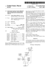
MODIFIED
COPS FLASH DEVICE
TARGETVCC
ICE LOGIC
lN-CIRCUIT EMULATOR
.
1 h
d . h h
1 .
b
d
e 51g“? 55 are W“ t e emu anon 21,56 are route
P[RIOCNESOLR
U.S. Patent
Dec. 7, 2004
Sheet 1 0f 10
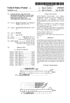
FIGURE 1a.
‘06
101
O
O
‘III
102
gr madam’
iceMASTER - WA
FIGURE 1b.
US 6,829,727 B1
103
U.S. Patent
:WZQEIG-.L
Dec. 7, 2004
Sheet 3 0f 10
US 6,829,727 B1
.OEZwm
.EOa 0. 04
m
wEom3No5Q0
-_1.
‘
m
H
‘
m
261
mmMDQE
m
w
.nE Q m.EmF5ZQ:
om
Il Il lII0ii-\|lIilI
Enmwtz
A
U.S. Patent
Dec. 7, 2004
Sheet 4 0f 10
CLK
2%
q:
%
%
‘J
ZZZ
z
5'.
§
*5
O
g’,
@-
s
CTL. DATA 1.0
5
E
a
a
ht’
E
E
Q
|
I
C)
Q
m
O
PMINTEPRFUACTE
(from FIG. 5)
FIGURE 4a.
US 6,829,727 B1
U.S. Patent
Dec. 7, 2004
Sheet 5 0f 10
DAT ..0
US 6,829,727 B1
CP DATA ..O
PCIRONTESFOALCRE
N CPRD
N
8
CP CLK
N TAR RESET
PCRONTESOLR
TARGET
m
E
c
Q.
{iE
Q:
(J
M
1.1.;
FIGURE 4b.
TARGET
U.S. Patent
Dec. 7, 2004
Sheet 6 0f 10
nag:Iva “Ema @5 SoEdge
‘ POUT FLAG
SILO]
‘T1LAGS 4.0]
OUT DATA 7..0
FIGURE 5a.
US 6,829,727 B1
U.S. Patent
Dec. 7, 2004
Sheet 7 0f 10
US 6,829,727 B1
NTMRD
TM DR 16..[)
AMcUERoIBOmUTYE
FIGURE 5b.
TMERAOCREY
AMUERIBOURTYE
U.S. Patent
Dec. 7, 2004
Sheet 8 0f 10
US 6,829,727 B1
FIGURE 6. OUTPUT PIN FIELD LAYOUT
SLOTI I SLOTZ I 51073 I sum |
CLKPIN
swum I smusz
STATUS HELD
FIGURE 7v TYPE I WAIIEFORM
I
SLOT
I
ELK PIN
OUTPUTPIN
FIGURE 8. TYPEZWAVEFORM
I SLOT
I
[11K PIN
OUTPUTPIN
FIGURES. TYPELIWAVEFORM
|
IZLK PIN
UUTI’UTPIN
SLOT
I
DAIAO
I
mm
I sumo I
‘ ~ '
L
| . . . .
I
HELD
—-I—
DATA? J
U.S. Patent
Dec. 7, 2004
US 6,829,727 B1
Sheet 9 0f 10
FIGURElO. TYPE4WAVEFORM
|
SLOT
|
IILII PIN
001001 PIN
FIGURE II. POUT PIN FIELD LAYOUT
copemcnmuvm
SLOT]
SLOTZ
SLOT3 I
SLOTS
II
CLK PIN
4 —
PCSTATUSFIELD
— >4 —-—
—IIONFIGURATION
—
—
+4 M
REGISTER FIELD
——
-
DILTA
FIGUREIZ. INPUT PIN FIELD LAYOUT
SLUT 10
0K PIN _J
51.071
I
swra I
SLOTZ I
Li
F— 0000000000 -
I
DATAO
—
|
—~ —
mum
--
——
REGISTER FIELD
I . .
INPUTDATA FIELD
SLOI 9
I
—
—
U.S. Patent
Dec. 7, 2004
Sheet 10 0f 10
US 6,829,727 B1
wOS
NV
méz?w
M.20wO3H52UD0mO‘Z_E5:Q
xN.2,mwo?z
E6$00GmUimN 5No$000x0
5.m2 o9z5aoQ
0mi% E00.7Eno8mQi32
E
200
w
m
0
r
w
i
m
m
v
.
00
$00
G
00
o
Q
0
g
;
m
. 00>O
NF
US 6,829,727 B1
1
2
IN-CIRCUIT EMULATION OF SINGLE CHIP
MICROCONTROLLERS
volume of the part. While a typical microcontroller in
production can run in the millions of units per year, Bond
Out chip consumption typically numbers in the tens to
hundreds of units per year. Also, cost is added to the Bond
Out chip by its use of larger packaging and special test How
due to the extra pins and associated functionality. This
BACKGROUND OF THE INVENTION
1. Field of the Invention
This invention relates to the in-circuit emulation of
microprocessors, speci?cally to an improved method of
emulating COP8® microcontrollers.
results in a more expensive emulator and a higher cost of
repair (the most common failure in an ICE system is the
Bond Out chip).
10
It is generally recognized that real-time in-circuit emula
part. The production part is alWays the focus of improve
ments through bug ?xes, yield improvements and die
tors (ICE) are a desirable, and in many cases, a necessary
tool for engineers involved in designing applications that use
an embedded microprocessor. An ICE alloWs the engineer to
exercise direct control over the execution of his application
program being run on the microprocessor. This control
enables the engineer to determine if a program is performing
as expected, and in the case Where it is not, the ICE makes
it much easier to debug the program.
15
in cases Where the Bond Out is physically a separate die,
although it can also happen Where the Bond Out is a package
option due to limitations on test development resources.
When this divergence occurs, the ICE becomes less useful as
a real-time emulator.
An ICE typically has some type of probe that replaces the
A fourth disadvantage is that a neW Bond Out chip is
required When the semiconductor manufacturer decides to
add neW functionality to a microcontroller by designing and
circuit board. Through an interface, usually hosted on a
standard Personal Computer, an engineer can use the ICE to
25
locations or events or vieW a snapshot of his program’s
An ICE is designed around the address and data bus of the
microprocessor. It monitors and controls the How of
addresses and data on the microprocessor’s busses and
interfaces are added, or When there are architectural
enhancements. This can get particularly burdensome When
one considers that usually tWo to four new, functionally
thereby provides the features used by the engineer to control,
different microcontrollers are introduced every year for
test and debug a program. HoWever, a special case arises
common and popular microcontroller architectures.
These different functional variations also impact the ICE
manufacturer, since a neW ICE Probe has to be designed for
each neW Bond Out chip. In addition to the development
With a class of embedded microprocessors called single chip
microcontrollers such as the National Semiconductor COPS
family. There is no address and data bus. These microcon
trollers execute their program out of an internal non-volatile
code memory such as a ROM, EPROM or Flash.
To provide the advantages of an ICE to their customers,
address and data bus on extra pins. Using extra pins alloWs
the address and data bus to be available to the ICE While at
producing neW versions of the microcontroller. A neW Bond
Out is required for each neW functional variation. While a
neW Bond Out chip is not needed if the neW variation of the
microcontroller is simply less memory or feWer IO pins, it
is required Whenever neW on-chip peripherals or neW I/O
execution history.
microcontroller manufacturers generally develop a special
version of the single chip microcontroller, called a Bond Out
chip. ABond Out chip disables the internal code memory of
the single chip microcontroller and brings out the internal
shrinks. The Bond Out, due to its limited use, often doesn’t
share in these improvements. This most commonly happens
actual microprocessor on the engineer’s application printed
vieW and modify the microprocessor’s internal state, start
his program at speci?c locations, stop his program at speci?c
A third disadvantage is that over the lifetime of the
product, it is not unusual for the Bond Out chip’s operating
parameters and functionality to diverge from the production
2. Related Art
costs involved, it also delays the availability of the ICE for
many months While the ICE system With the neW Probe is
40
debugged, tested and released to production. This prevents
early users of the microcontroller from being able to develop
their applications With the aid of an ICE. Since many design
engineers Will not use a microcontroller unless there is an
ICE available for it, this delay can also sloW the acceptance
45 of a neW microcontroller.
the same time preserving the chip’s 1/0 that the user’s
application is using. These Bond Out chips are made avail
able to ICE manufacturers so they can develop an ICE for
the chip.
While a Bond Out chip alloWs an ICE to be built for a
single chip microcontroller, it nonetheless has several dis
advantages. First, because of the extra pins needed, it is
packaged in a larger package than the standard production
SUMMARY OF THE INVENTION
Objects of the Invention
1. An object of one aspect of the invention is to provide
circuitry in a modi?ed COPS to alloW real-time in-circuit
emulation Without the need of an address/data bus or
Bond Out chip by using the standard production micro
controller.
microcontroller. This means that it cannot be used in the site 55 2. An object of one aspect of the invention is to alloW
that the production part Will occupy on the target system.
Rather the Bond Out chip is placed on an ICE Probe or
resides in the ICE base unit and the pin signals are connected
to the target system through a cable or an adapter. Not
operating in the actual application board site causes severe
degradation of analog signals and often limits the environ
mental parameters (e.g., temperature) in Which the system
can be emulated and debugged.
A second disadvantage of the Bond Out chip is its higher
emulation of microcontrollers With integrated high per
formance analog peripherals Without degrading the ana
log performance.
3. An object of one aspect of the invention is to alloW
emulation of the COPS in the actual environment in Which
it is going to be used Without having to “ruggediZe” the
emulator to handle hostile conditions.
4. An object of one aspect of the invention is to alloW the
user’s target system to be easily sWitched by means of a
cost, Which in some cases can be as high as ten times the cost 65
standard, simple connector betWeen a development sys
of the production microcontroller. Several factors contribute
tem that interfaces to the emulator and a ?nal production
system that can be shipped to a customer.
to the cost of a Bond Out chip. One is the relatively low
US 6,829,727 B1
4
3
5. An object of one aspect of the invention is to provide
FIG. 3 is a block diagram of a microcontroller in accor
dance With the present invention.
FIG. 4 is a block diagram of the core ICE Logic.
FIG. 5 is a block diagram of the extended features ICE
circuitry in a modi?ed COPS to allow a range of emula
tors.
6. An object of one aspect of the invention is to require a
minimal number of modi?ed COPS pins needed to inter
face to the emulator to alloW for small pin count micro
controllers.
7. An object of one aspect of the invention is not to rely on
Logic.
FIG. 6 shoWs the OUTPUT pin ?eld layout.
FIG. 7 shoWs a Type 1 Waveform.
an external clock as a timing source and be clocking
scheme independent.
8. An object of one aspect of the invention is to be able to
10
FIG. 9 shoWs a Type 3 Waveform.
detect internal Resets so as to alloW emulation of COPS
microcontrollers Without an external Reset pin.
9. An object of one aspect of the invention is the ability to
recreate the COPS digital pins that interface to the emu
lator and that these pins can have multiplexed
FIG. 10 shoWs a Type 4 Waveform.
15
functionality, not just simple digital I/O.
DETAILED DESCRIPTION
gramming during emulation.
11. An object of one aspect of the invention is to provide for
communication betWeen the emulator and an on-chip
monitor program to alloW full visibility to the state of the
microcontroller.
In the folloWing description, numerous speci?c details are
set forth to provide an understanding of the present inven
tion. It Will be apparent hoWever, to those skilled in the art
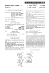
Brie?y, the present invention provides a system and
25
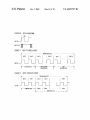
COPS microcontroller using the standard production device
block is a ?ash-memory based microcontroller 201 having a
slightly modi?ed COPS architecture. The second block is the
necessarily all referring to the same embodiment.
Furthermore, various particular features, structures, or char
emulator logic, the ICE Logic 202, and the third block is the
Control Processor 203 that interfaces betWeen the ICE Logic
acteristics may be combined in any suitable manner in one
and the user interface running on a standard Personal
35 or more embodiments.
One embodiment of a method of the present invention
uses four digital pins of a ?ash-memory based COPS micro
controller that are recon?gured in emulation mode to output
clock, status and data to the ICE Logic and an input pin to
1.0 COPS Architecture, Machine Cycle and Timing
The COPS is an 8-bit accumulator based, Harvard archi
40
tecture microcontroller With a maximum program memory
45
space of 32 Kbytes. As a microcontroller, all of its program
memory and data memory resides on-chip. It has no external
bus. The program memory of all COPS versions used With
this invention is implemented as ?ash memory.
In addition to memory, different versions of the COPS
pin’s data communicates With a small ROM-based monitor
in the COPS and provides a means of inputting and output
ting the internal state of the machine as Well as programming
the ?ash memory in-circuit. Those skilled in this ?eld and
having the bene?t of the present disclosure Will understand
that although the term “pin” is used, the present invention is
an
embodiment”, means that a particular feature, structure, or
characteristic described in connection With the embodiment
is included in at least one embodiment of the present
invention. The appearance of such phrases herein are not
printed circuit board. The system of the present invention, as
shoWn in FIG. 2, contemplates three major blocks. The ?rst
input commands and data from the ICE Logic. The input
and having the bene?t of this disclosure, that the present
invention may be practiced With apparatus and processes
that vary from those speci?ed herein.
Reference herein to “one embodiment”, or
directly soldered or otherWise connected on the application’s
Computer.
FIG. 11 shoWs the POUT pin ?eld layout.
FIG. 12 shoWs the INPUT pin ?eld layout.
FIG. 13 shoWs the signal layout on the ICE Logic
connector.
10. An object of one aspect of the invention is to alloW the
use of on-chip ?ash memory and alloW in-system pro
method of providing real-time in-circuit emulation of a
FIG. 8 shoWs a Type 2 Waveform.
also have different amounts and types of peripherals on-chip.
Some common examples of these on-chip peripherals
include timers, digital I/O ports, an interrupt controller and
not limited to use With microcontrollers having pins, but
may be used With any type of mechanism by Which electrical
connection is made to a packaged semiconductor device,
A/D converters.
including but not limited to solder bumps, solders balls, and
The COPS basic machine cycle consists of ten clock
lands.
The system and method alloW a user sitting at his Personal
Computer to use the system as a fully functional, real-time
in-circuit emulator. The user Will be able to load and patch
his program in the on-chip ?ash of the COPS; run the
periods. Each clock period is referred to as a Slot. So a
program or single step through it, set breakpoints; vieW and
change the state of any user-visible memory or register. In
addition, optional functions can be added to provide addi
tional debugging capabilities such as code trace and hard
Ware attributes.
BRIEF DESCRIPTION OF THE DRAWINGS
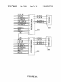
FIG. 1 is a pictorial vieW of the emulation system,
including the ICE, the COPS and an application printed
circuit board.
FIG. 2 is a block diagram of the emulation system,
including the ICE, the COPS and the application.
machine cycle consists of Slot 1 through Slot 10. The
instruction set consists of one-byte, tWo-byte and three-byte
instructions. The shortest instructions execute in one
55
machine cycle. The longest instruction executes in seven
machine cycles.
The instruction set is composed of arithmetic, logical,
memory transfer and transfer of control instructions. The
arithmetic and many of the logical instructions use the
accumulator as the destination operand. Several of the
logical instructions either skip or execute the next instruc
tion depending on the result. There are different transfer of
control instructions With a —31/+=byte range, a 2 Kbyte page
65 range or a 32 Kbyte range.
For a more detailed description of the COPS refer to
National Semiconductor’s COPS Family User’s Manual.
US 6,829,727 B1
5
6
2.0 Modi?ed COPS Core
4.0 Details of the Ice Monitor
In one aspect of the present invention the standard COPS
In one embodiment of the present invention the ICE
architecture Was modi?ed . First, a small amount of read
Monitor is a program of approximately 512 bytes in length
that is physically implemented as a non-programmable Read
only memory (ROM) Was added beyond the 32 K program
memory address space. This ROM contains the in-system
programming (ISP) ?ash memory read/Write routines and a
monitor (ICE Monitor) program that interfaces to the ICE
Logic. This ROM is called the Monitor ROM.
Second, tWo neW instructions Were added to the COPS
instruction set. The ?rst instruction is a softWare breakpoint
Only Memory (ROM) logically located outside the standard
32 Kbyte COPS program memory space. The ICE Monitor
program receives and executes commands that are sent to it
10
instruction (assembly code mnemonic: BRK). This instruc
tion pushes the current program counter (PC) onto the stack
and jumps to the ICE Monitor. The second instruction is a
return to ?ash instruction (assembly code mnemonic:
RETF). This instruction pops the PC from the stack and
starts executing in the ?ash memory (standard program
15
the stack. The ?rst instructions of the ICE Monitor are used
to output the A, PSW, B and X registers to the ICE Logic.
These registers are used by the ICE Monitor in executing its
memory address space).
Third, four digital I/ O pins Were re-con?gured to interface
to the ICE. One of these four pins outputs a clock. This clock
is of the same frequency as that used by the COPS CPU. All
by the ICE Logic. The ICE Monitor program may be stored
in a ROM of any suitable design. Furthermore, the present
invention is not limited to the particular type of storage
medium in Which the ICE Monitor program is stored.
Execution of the ICE Monitor begins When the modi?ed
COPS detects a breakpoint and jumps to the ICE Monitor
entry point after pushing the current program counter onto
20
information passed on the other three pins is done synchro
commands and this initial action preserves their values as
used in the user’s program context. These values are restored
to the registers before the system exits the ICE Monitor and
returns to emulating the user’s program (see sections 4.1.7
nous to this clock. TWo of the remaining three pins are used
EMULATION RESET COMMAND and 4.1.8 EMULA
to output cycle and instruction synchroniZation ?ags, state,
TION GO COMMAND).
After outputting the four registers, the ICE Monitor
status, internal data and port recreation information. The last
of the four pins is an input pin that is used by the ICE to input
control, recreated port, command and Write data informa
25
program, in accordance With one embodiment of the present
tion.
3.0 Details of the NeW Instructions
3.1 BRK—SoftWare Breakpoint
The softWare breakpoint instruction (BRK—opcode
0x62) pushes the return address onto the stack in data
memory and then jumps to a ?xed address in the Monitor
ROM. The execution of this instruction also sets the Break
state signal in the modi?ed COPS. The jump to the Monitor
ROM and the setting of the Break state only occurs if the
modi?ed COPS is in ICE Hooks mode (see section 6.0,
“Details of Enabling the ICE Hooks mode”).
During the execution of the BRK instruction, the contents
of the PCL (loWer S bits of the program counter) are
transferred to the data memory location referenced by the SP
30
command. Commands are available to read and Write the
data memory RAM, the special function registers and the
35
that is the entry point into the Monitor ROM. The CPU then
starts executing the program in the Monitor ROM at that
address.
4.1.1 Data Memory Read Command
40
45
The <Starting Address> is the address of the ?rst location to
be read.
The <Count> is the number of locations to be read.
50
The return to ?ash instruction (RETF—opcode 0x63)
55
execution of this instruction also clears the Break state
signal in the COPS.
During the execution of the RETF instruction, the SP is
next command.
60
the PCU, after Which the SP is again incremented. Next, the
contents of the data memory location referenced by the SP
are transferred to the PCL. The return address has noW been
retrieved from the stack in data memory RAM. The CPU
then starts executing the program in the ?ash memory at the
return address.
In executing this command, the ICE Monitor reads the
value at the starting address and outputs it to the ICE Logic.
It then decrements the Count value. If the decremented
Count value is not Zero, it increments the Starting Address
value, reads the value at the neW address, outputs it to the
ICE Logic and decrements the Count value again. This
continues until the Count value is equal to Zero. When the
Count value is Zero, this routine exits through a common end
of command routine and returns to the idle loop to aWait the
memory (standard program memory address space). The
?rst incremented. The loWer seven bits of the byte at the data
memory location referenced by the SP are then transferred to
byte values from the modi?ed COPS internal data memory
and its special function registers and output the values to the
ICE Logic. This command is three bytes long and is of the
form:
<01>: <Starting Address> <Count>
The ?rst byte, <01>, is the command value that is decoded
by the command decoder.
3.2 RETF—Return from Subroutine to Flash
pops the return address from the stack in data memory and
then begins execution at the return address in the ?ash
?ash program memory. In addition, commands are used to
return the modi?ed COPS into emulation mode Where it
executes the User’s program Which is stored in ?ash
memory.
4.1 Details of the Ice Monitor Commands
The DATA MEMORY READ command is used to read
(stack pointer). The SP is then decremented, folloWed by the
contents of PCU (upper 7 bits of the program counter) being
transferred to the neW data memory location referenced by
the SP. The return address is noW saved on the stack in data
memory RAM. Then the SP is decremented again to set up
the stack reference for the next subroutine.
Next, the program counter is loaded With a ?xed address
invention, then enters a loop (idle loop) Waiting for a
command byte from the ICE Logic. Once a command byte
is received, the ICE Monitor decodes the command,
executes it and then returns to the idle loop aWaiting the next
65
4.1.2 Data Memory Write Command
The DATA MEMORY WRITE command is used to input
byte values from the ICE Logic and Write the values to the
modi?ed COPS internal data memory and its special func
tion registers. This is a variable length command and is of
the form:
<02> <Starting Address> <Count> <Byte 1> <Byte 2> . . .
US 6,829,727 B1
8
7
ISPADHI—High byte of the starting address
ISPADLO—LoW byte of the starting address
The ?rst byte, <02>, is the command value that is decoded
by the command decoder.
The <Starting Address> is the address of the ?rst location to
be Written.
The <Count> is the number of bytes remaining to be sent in
4.1.3 Program Memory Read Command
COUNT—Number of bytes to Write
X—Starting address in RAM of the Write buffer
The loW-level ISIP routine reads <COUNT> bytes from the
buffer in the modi?ed COP8 internal data memory starting
at address <X> and Writes the bytes into the ?ash memory
starting at address <ISPADHI><ISPADLO>.
Before the PROGRAM MEMORY WRITE command is
sent to the ICE Monitor, the ICE Logic loads the appropriate
values in the ISPADHI, ISPADLO and COUNT registers
using the DATA MEMORY WRITE command.
This command is tWo bytes long and is of the form:
<04> <Buffer Address>
The ?rst byte, <04>, is the command value that is decoded
by the command decoder.
The <Buffer Address> is the starting address of the buffer in
the modi?ed COP8 internal data memory Where the bytes to
The PROGRAM MEMORY READ command is used to
be Written to the ?ash memory are stored.
the command as Well as the number of locations to be
Written.
<Byte 1> <Byte 2> . . . <Byte n> are the values to be Written.
In executing this command, the ICE Monitor inputs <Byte
1> from the ICE Logic and Writes it to the starting address.
It then decrements the Count value. If the decremented
Count value is not Zero, it increments the Starting Address
10
value, inputs the next byte from the ICE Logic, Writes this
value to the neW address and decrements the Count value
again. This continues until the Count value is equal to Zero.
When the Count value is Zero, this routine exits through a
common end of command routine and returns to the idle
loop to aWait the next command.
15
read byte values from the modi?ed COP8 ?ash program
memory and Write them to a buffer located in the modi?ed
COP8 internal data memory.
This command uses the loW-level ISP ?ash memory read
routine. This loW-level ISP routine requires the folloWing
25
registers to be set up before it is called:
ISPADHI—High byte of the starting address
ISPADLO—LoW byte of the starting address
memory, it returns to this command routine. This routine
then exits through a common end of command routine and
returns to the idle loop to aWait the next command.
COUNTHI—High byte of the number of bytes to read
COUNTLO—LoW byte of the number of bytes to read
X—Starting address in RAM of the read buffer
The
loW-level
ISP
routine
reads
<COUNTHI><COUNTLO> bytes of the ?ash memory
starting at address <ISPADHI><ISPADLO> and stores the
bytes in the modi?ed COP8 internal data memory starting at
address <X>.
Before the PROGRAM MEMORY READ command is
sent to the ICE Monitor, the ICE Logic loads the appropriate
values in the ISPADHI, ISPADLO, COUNTHI and
COUNTLO registers using the DATA MEMORY WRITE
command.
This command is tWo bytes long and is of the form:
<03> <Buffer Address>
The ?rst byte, <03>, is the command value that is decoded
by the command decoder.
The <Buffer Address> is the starting address of the buffer in
4.1.5 Program Memory Page Erase Command
The PROGRAM MEMORY PAGE ERASE command is
used to erase a page of the ?ash memory. Apage is typically
64 or 128 bytes in siZe. The ?ash memory has to be erased
35
40
ISPADHI—High byte of the starting address of the page
to be erased
ISPADLO—LoW byte of the starting address of the page
to be erased
The loW-level ISP erases a page of ?ash memory starting at
45
the <ISPADHI><ISPADLO> page boundary.
Before the PROGRAM MEMORY PAGE ERASE com
mand is sent to the ICE Monitor, the ICE Logic loads the
In executing this command, the ICE Monitor stores the
<Buffer Address> in the X register. It then calls the loW-level
ISP read routine that is part of the Monitor ROM. The ISP
routine reads the number of bytes requested starting at the
55
appropriate values in the ISPADHI and ISPADLO registers
using the DATA MEMORY WRITE command.
This command is one byte long and is of the form:
<05>
The byte <05> is the command value that is decoded by the
command decoder.
In executing this command, the ICE Monitor calls the
loW-level ISP page erase routine that is part of the Monitor
ROM. The ISP routine erases a page of ?ash memory
memory, it returns to this command routine. This routine
then exits through a common end of command routine and
returns to the idle loop to aWait the next command.
starting at the speci?ed page boundary. When the ISP routine
is done erasing the ?ash memory, it returns to this command
routine. This routine then exits through a common end of
command routine and returns to the idle loop to aWait the
4.1.4 Program Memory Write Command
The PROGRAM MEMORY WRITE command is used to
Write byte values to the modi?ed COP8 ?ash program
memory from a buffer located in the modi?ed COP8 internal
data memory.
This command uses the loW-level ISP ?ash memory Write
before neW values can be Written to it.
This command uses the loW-level ISP ?ash memory page
erase routine. This loW-level ISP routine requires the fol
loWing registers to be set up before it is called:
the modi?ed COP8 internal data memory Where the read
?ash memory bytes are stored.
?ash memory address speci?ed and stores them in the
internal data memory buffer starting at the address contained
in X. When the ISP routine is done reading the ?ash
In executing this command, the ICE Monitor stores the
<Buffer Address> in the X register. It then calls the loW-level
ISP Write routine that is part of the Monitor ROM. The ISP
routine reads the number of bytes requested from the inter
nal data memory buffer starting at the address contained in
X and Writes them to the ?ash memory starting at the address
speci?ed. When the ISP routine is done Writing the ?ash
next command.
4.1.6 Program Memory Mass Erase Command
The PROGRAM MEMORY MASS ERASE command is
routine. This loW-level ISP routine requires the folloWing
used to erase the complete ?ash memory (up to 32 Kbytes)
implemented in the modi?ed COP8. The ?ash memory has
registers to be set up before it is called:
to be erased before neW values can be Written to it.
65
US 6,829,727 B1
9
10
This command is one byte long and is of the form:
<06>
The byte <06> is the command value that is decoded by the
command decoder.
In executing this command, the ICE Monitor calls the
ICE Logic can input data to the ICE Monitor faster than it
can process it. If the modi?ed COPS is running at its
maximum frequency, the ICE Monitor can output data faster
than the ICE logic can process it. Because of this Wide range
loW-level ISP mass erase routine that is part of the Monitor
ROM. The ISP routine erases the complete ?ash memory
must synchroniZe the data transfers betWeen them.
Whenever the ICE Monitor is Waiting for data from the
ICE Logic, it is executing a small loop polling a received
byte status ?ag. In this loop no instructions are skipped.
When a byte sent from the ICE Logic has been loaded into
the ICE Monitor’s receive register, the ICE Monitor detects
the received byte status ?ag is asserted and skips an instruc
tion Which causes the modi?ed COPS to output a Skip Flag
of operating conditions, the ICE Monitor and ICE Logic
implemented in the microcontroller. When the ISP routine is
done erasing the ?ash memory, it returns to this command
routine. This routine then exits through a common end of
command routine and returns to the idle loop to aWait the
10
next command.
4.1.7 Emulation Reset Command
on the OUTPUT pin (see Section 5.2). The ICE Logic
The EMULATION RESET command is used to start
detects this Skip Flag and knoWs that the byte Was received.
execution of the user’s program from a reset.
15 Once the ICE Monitor has read the byte from its receiver
This command is four bytes long and is of the form:
register, it again skips an instruction. When the ICE Logic
detects a second Skip Flag after sending a byte, it knoWs that
<07> <X> <B> <A>
The byte <07> is the command value that is decoded by the
command decoder.
The <X> is the value for the X register.
The <B> is the value for the B register.
The <A> is the value for the A register.
In executing this command, the ICE Monitor restores the
X, B and A registers to the values that Were previously set
by the user’s program. The PSW register is not restored
since it is initialiZed by a Reset. After restoring the last
the ICE Monitor has consumed the byte and it is safe to send
another byte. This Skip Flag synchroniZation prevents the
ICE Logic from overrunning the ICE Monitor’s receive
register.
Whenever the ICE Monitor is prepared to send data to the
ICE Logic, it Waits in a loop until it gets a signal from the
25
register, this routine stays in a loop Waiting for the modi?ed
sending the byte that gates the ICE Monitor. Upon receiving
COPS to be Reset. When the ICE Logic asserts Reset to the
the byte, the ICE Monitor throWs it aWay, skips an
microcontroller’s RESET pin, the Break state signal is
cleared. After Reset is de-asserted, the modi?ed COPS Will
start execution at address 0000 of the ?ash memory (user’s
instruction, outputs the pending data to the ICE Logic and
skips another instruction. If the ICE Monitor has more data
to send, it again loops Waiting for the ICE Logic to send the
gating byte. When the ICE Logic detects the ?rst Skip Flag
program).
This command can be abort before Reset is asserted. If the
in this sequence it knoWs that the ICE Monitor has seen its
ICE Monitor receives a byte from the ICE Logic While it is
looping, it Will fall through the loop and exit through a
35
common end of command routine and return to the idle loop
to Wait for a neW command.
byte from its receiver buffer. This gating byte synchroniZa
The EMULATION GO command is used to start execu
tion prevents the ICE Monitor from overrunning the ICE
40
This command is ?ve bytes long and is of the form:
<08> <X> <B> <PSW> <A>
The byte <08> is the command value that is decoded by the
command decoder.
The <X> is the value for the X register.
The <B> is the value for the B register.
The <PSW> is the value for the PSW register.
The <A> is the value for the A register.
45
information.
55
The G3 (CLK) pin outputs a clock of the same frequency
as that used by the modi?ed COPS CPU. This pin outputs 10
clocks per machine cycle. All information passed on this
interface (except external Reset) is done synchronously to
this clock. This pin is alWays clocking except When the
modi?ed COPS is in HALT mode, IDLE mode or the CKI
clock has been lost. The signal on this pin is referred to as
CLK in the folloWing descriptions.
5.2 G2—OUTPUT
4.2 Ice Monitor and Ice Logic Synchronization
The G2 (OUTPUT) pin outputs synchroniZing, state,
The COPS in a user’s application can run at any arbitrary
frequency up to the maximum permitted by the device
ured to interface to the ICE Logic. The four pins are the
loWer four bits of the G Port commonly referred to as G0,
G1, G2 and G3. G3 is recon?gured to output the CPU clock.
input control, target pin data, command and Write data
set by the user’s program. This routine then executes a RETF
instruction that clears the Break state signal and pops an
address off the softWare stack and loads it into the program
counter. Execution of the user’s program in ?ash memory
begins at this neW value in the program counter.
speci?cation. The ICE Logic runs at a ?xed speed. If the
modi?ed COPS is running at a relatively loW frequency, the
Logic’s receive buffer.
5.0 Details of the Recon?gured Digital IO
Four of the modi?ed COPS digital I/O pins are recon?g
G2 is recon?gured to output synchroniZing, state, status and
internal data information. G1 is recon?gured to output the
program counter update status and the output state of the
four G Port pins used in this interface. G0 is recon?gured to
Before the EMULATION GO command is sent to the ICE
Monitor, the ICE Logic loads the address Where the user
Wants his program to begin executing. This address is placed
on the top of the softWare stack using the DATA MEMORY
WRITE command.
In executing this command, the ICE Monitor restores the
X, B, PSW and Aregisters to the values that Were previously
signal and is preparing to output its data. Upon detecting the
second Skip Flag, the ICE Logic knoWs that the ICE
Monitor has output its pending data and is ready to send
another byte. The ICE Logic can then read the transferred
4.1.8 Emulation Go Command
tion of the user’s program at a speci?c address. The address
Where execution Will begin is on the top of the softWare
stack in the modi?ed COPS internal data memory.
ICE Logic that it is ready to receive the byte. The ICE Logic
signals its readiness by sending a byte to the ICE Monitor.
The value of the byte is super?uous. It is the action of
65
status and internal data information. There is a signi?cant
amount of information that is transferred on this pin to the
ICE Logic. The folloWing list summariZes by group the
transferred information:
US 6,829,727 B1
11
12
Synchronizing signals:
Machine cycle synchronization (First clock of machine
Type 2 Waveform—LOW voltage at negative CLK edge,
HIGH voltage level at POSiIiVe CLK edge
Cycle)
Decoded by the ICE Logic as a Sync bit With a ‘1’ logic
Instruction cycle synchronization (Fetch signal, ?rst byte
value,
of an instruction)
State signals:
COPS executing in Break mode (running ICE Monitor)
COPS executing in Emulation mode (running User
program)
FIG. 8. Type 2 Waveform
10
Status signals:
I Slot
Skipped Instruction (current instruction is being skipped)
I
CLKPin
PL/PU replacement When a program transfer occurs
Internal data signals:
Internal data bus
15
OUTPUT Pin
XXXX _/
XXXX
The OUTPUT pin breaks the 10-slot COPS machine cycle
into tWo ?elds (see FIG. 6): the Status Field and the Data
Field. COPS internal data is alWays output in the Data Field.
_
The remaining synchronization, state and status information
is encoded in the tWo slots of the Status Field.
Type 3 WaVef0rm—LOW Voltage at negatlve CLK edge,
LOW voltage at positive CLK edge.
FIG. 6. OUTPUT Pin Field Layout
I <- ---------------------------- -- COPS Machine Cycle ---------------------------- ---> I
I
CLKPin
Slot 1
/ I
Status1
I
Status
I
Slot 2
I
I
Slot 3
DataO
I
Slot 4
I
Data1
I
I
°I ' °' '
Slot 10
I
I
Status2
I
Data7
I
Field
I <- ———————————————————— — — Data Field ———————————————————— — — —>
I
35
There are four Waveform types that are used to encode the
information in the Status Field. These Waveform types are
Decoded by the ICE Logic as a ‘0’ logic value.
FIG. 9. Type 3 Waveform
referred to as Type 1, Type 2, Type 3 and Type 4 Waveforms.
Type 1 and Type 2 Waveforms are bi-phase signals and are 40
only found in the Status Field of the OUTPUT signal. A
I Slot
Type 1 or Type 2 Waveform is also called a Sync bit since
CLK Pin
I
/ —\
they are used to synchronize the ICE Logic and COPS on a
—
/—
—
machine cycle, instruction cycle and state basis. The four
45
OUTPUT Pin
XXXX — XXXX
Waveforms are de?ned as folloWs:
Type 4 Waveform—HIGH voltage at negative CLK edge,
HIGH voltage level at positive CLK edge.
Type 1 Waveform—HIGH voltage at negative CLK edge,
LOW V01tag6 at POSiIiVe CLK edge
50
Decoded by the ICE Logic as a ‘1’ logic value.
FIG. 10. Type 4 Waveform
Decoded by the ICE Logic as a Sync bit With a ‘0’ logic
value.
I Slot
I
FIG. 7. Type 1 Waveform
OUTPUT Pin
|—S1Ot
CLK Pin
|—
_/
XXXX
XXXX
Status1 (Slot 1) Information—Machine and Instruction
synchronization. The OUTPUT signal in Slot 1 is used to
synchronize the ICE Logic to the modi?ed COPS on both a
OUTPUT Pin
XXXX
\
XXXX
machine cycle and instruction cycle basis. During normal
65 execution, this slot Will alWays contain either a Type 1 or a
Type 2 Waveform. Since there are no Sync bits in the Data
Field of the OUTPUT signal, the ?rst slot With a Sync bit
US 6,829,727 B1
14
13
following a slot With no Sync bit identi?es it as Slot 1
Decoding Slot 2 logic value information depends on the
(machine synchronization). The type of Sync bit (Type 1 or
presence or absence of a Slot 1 Fetch ?ag. If Slot 1 contains
Type 2) identi?es Whether or not this is the ?rst cycle of an
a Fetch ?ag, the logic value of this slot is used to specify
Whether or not the current instruction is being skipped. A
instruction (instruction synchronization). A Type 2 Wave
form signals the ?rst cycle of an instruction and is de?ned
as a Fetch ?ag.
logic value of ‘1’ (Type 2 or Type 4 Waveform) speci?es that
the current instruction is being skipped.
The ICE Logic also uses the absence of Sync bits to
decode internal resets. If there hasn’t been a Sync bit in the
last 10 CLK periods AND eXternal Reset has been
de-asserted, the ICE Logic Will decode this as the modi?ed
If Slot 1 does not contain a Fetch ?ag, the logic value of
this slot is used to specify Whether or not the loWer byte (PL)
or the upper 7-bits (PU) of the program counter (PC) had
10
COP8 is resetting internally.
Status2 (Slot 2) Information—State and Status. This slot
speci?es a PU/PL replacement. What part of the PC is
actually replaced is signaled by the POUT pin (see section
is used to pass the current state (Break or Emulation),
instruction status (skipped or not) and PC replacement status
(replace part of the PC or not). The eXact meaning of the
Status information in this slot depends on the information
decoded in Slot 1. See Table I for a complete listing of all
Slot 1 and Slot 2 combinations.
been replaced in the previous cycle. A logic value of ‘1’
5.3).
15
A special case of PL/PU replacement is an interrupt. The
POUT Pin is also used to signal that an interrupt is being
processed.
Data Field (Slots 3 to 10)—Data. The data is shifted out
from a COP8 internal data bus using only Type 3 or Type 4
Waveforms.
The presence or absence of a Sync bit in this slot
determines the State information. If a Sync bit is present the
modi?ed COP8 is in Break state. If there is no Sync bit, the
modi?ed COP8 is in Emulation state.
Summary of the OUTPUT Pin (G2)
TABLE I
Valid Slot Waveform Combinations
Slot 1
Slot 2
S3
S4
S5
S6
Type 1
Type 1
D0
D1
D2
D3
S7
S8
S9
S10 Meaning
D5
D6
D7 Not a Fetch, Break State
D[7 . . . O] of previous cycle contains internal
bus data
Type 1
Type 2
D0
D1
D2
D3
D5
D6
D7
Not a Fetch, Break State
Type 1
Type 3
D0
D1
D2
D3
D5
D6
D7
Not a Fetch, Emulation State
D[7 . . . O] of previous cycle contains PC data
D[7 . . . O] of previous cycle contains internal
bus data
Type 1
Type 4
D0
D1
D2
D3
D5
D6
D7
Type 2
Type 1
D0
D1
D2
D3
D5
D6
D7 Fetch, Break State
Not a Fetch, Emulation State
D[7 . . . O] of previous cycle contains PC data
D[7 . . . O] of previous cycle contains internal
bus data
Type 2
Type 2
D0
D1
D2
D3
D5
D6
D7 Fetch, Break State, Instruction skipped
D[7 . . . O] of previous cycle contains internal
bus data
Type 2
Type 3
D0
D1
D2
D3
D5
D6
D7 Fetch, Emulation State
D[7 . . . O] of previous cycle contains internal
bus data
Type 2
Type 4
D0
D1
D2
D3
D5
D6
D7 Fetch, Emulation State, Instruction skipped
D[7 . . . O] of previous cycle contains internal
bus data
Type 3
Type 3
Reset, Emulation State
Type 4
Type 3
Reset, Emulation State
D[7 . . . 0] contains no valid data
D[7 . . . 0] contains no valid data
US 6,829,727 B1
15
16
5.3 G1—POUT
The G1(POUT) Pih Outputs ihsmleheh sehree> PC update
The interrupt activity and PC activity information is used
in combination With the Fetch Flag and PC replacement
activity and the data that allows the ICE Logic to recreate the
output state of the four G Port digital I/O pins used in this
interface. This pin uses only Type 3 and Type 4 Waveforms. 5
The POUT pin breaks the 10_S1Ot COPS machine Cycle
t t
f th OUTPUT - F
th- d t th ICE L S a us 0
6
pm‘ mm 15 a a’ e
Ogle
recreates the PC as it eXecutes the User’s program. This
_
_
recreated PC can be stored in a Trace Memory in the ICE
into three ?elds (see FIG. 11): the PC Status Field, the
Con?guration Register Field and the Data Register Field.
Logic to Provide the User with a Snapshot of his Program’s
execution history.
FIG. 11. POUT Pin Field Layout
l <- —————————————————————————————————————— — — COP8 Machine Cycle ———————————————————————————————————————— ——-> I
I
Slot 1
|
Slot 2
|
Slot 3
l ,
I
Slot 6
|
Slot 7
l
I
Slot 1O
CLK Pin
|
PC Status Field
| <- ————————— —- Configuration ————————— ——-> I <- ———————————— —- Data ———————————— ——-> I
I
Register Field
|
Register Field
|
25
The Con?guration Register Field and the Data Register
Field are used by the ICE Logic to recreate the output
TABLE III
functionality of G0, G1, G2 and G3. For each G Port pin that
is recreated the modi?ed COP8 outputs one Con?guration
Register bit and one Data Register bit. These tWo bits allow 30
the ICE Logic to support the various types of output con
?gurations available on the modi?ed COP8 (see Table II).
When a pin is con?gured for simple I/ O, the modi?ed COP8
simply outputs an image of its internal Con?guration and 35
w
POUT Pin
Signals PC
OUTPUT Pin Signals
Data Register bits. For pins that are con?gured to use an
Alternate Function, the modi?ed COP8 outputs the appro-
FETCH
PL/PU
priate Con?guration and Data Register bit pattern t0 re?ect
FLAG REPLACEMENT
Status Field
—
SLOT 1
SLOT 2 PC ACTION
the output value of the function.
40
TABLE H
COP8 Output Port Driver Con?gurations
Con?guration
Data
Output Driver
Register Bit
Register Bit
O
O
Tri_state Output
O
1
Wear pull-up
1
1
0
1
Push-pull Zero output
PuSh_pun one Output
Con?guration
O
O
O
O
No Action — PC Frozen
O
O
1
0
PC Incremented
O
1
O
O
PCL Replaced
0
1
O
1
Fun 7 bits of PCH
0
1
1
1
LoWer 4 bits of PCH
1
NA.
X
0
PC Incremented
1
NA.
X
1
Interrupt
45
Replaced
Replaced
5O
In Slot 3 through Slot 6, the POUT pin shifts out the
Con?guration Register bits least signi?cant bit (LSB) ?rst.
_
N'A' _ NotApphcable
In Slot 7 through Slot 10, the Data Register bits are shifted
X ' Don’t care
out LSB ?rst. The ICE Logic shifts in this POUT data and 55
at the end of Slot 10 synchronously outputs the neW output
state to its recreated output pins, Which are connected to the
User’s target system_
As Shown in Table HL during heh'feteh eyeles (Fetch
Flag=0) the PC can stay the same, increment or have various
The PC Status ?eld is used to provide the ICE Logic With
parts replaced. These actions represent the complete set of
6O a 11 th e P0551‘b1 6 PC ac t'1on5 aval'1 a b1 e t 0 th 6 COPS ms
' t rue t'Ion
information
on the source of instructions
(Flash or Monitor
ROM), interrupt activity and PC activity When the Fetch
set. This alloWs the ICE Logic to faithfully recreate the PC
Flag is asserted on the OUTPUT pin, the logic value on the
and track the instruction hOW aeehrately- During a feteh
POUT pin during Slot 1 determines the Source of the
cycle the PC is either incremented or an interrupt is being
instruction. Alogic value of ‘0’ speci?es that the instruction 65 PIOCeSSed- If the ICE LOgiC deCOdeS an interrupt, it forces
is being fetched from the Flash Memory. Alogic value of ‘1’
the interrupt vector OXOOFF into its recreated PC to mimic
speci?es an instruction fetch from the Monitor ROM.
the actions of the modi?ed COP8.
US 6,829,727 B1
17
18
Summary of the POUT Pin (G1)
TABLE IV
Valid Slot 1 and Slot 2 Waveform Combinations
S1
S2
S3
S4
S5
S6
S7
S8
S9
S10
Meaning
0
O
GCO
GC1
GCZ
GC3
GDO
GD1
GDZ
GD3
0
1
GCO
GC1
GCZ
GC3
GDO
GD1
GDZ
GD3
Fetch — Fetch from Flash
Not Fetch — PC frozen last cycle
Fetch — Fetch from Flash, Interrupt
1
O
GCO
GC1
GCZ
GC3
GDO
GD1
GDZ
GD3
1
1
GCO
GC1
GCZ
GC3
GDO
GD1
GDZ
GD3
Not Fetch — Full PCU replaced last cycle
Fetch — Fetch from ICE Monitor
Not Fetch — PC incremented last cycle
Fetch — Fetch from ICE Monitor, Interrupt
Not Fetch — 4 LSBs of PCU replaced last cycle
is used by the ICE Logic to input commands and data to the
5.4 GO—INPUT
The G0 (INPUT) pin inputs control, command, Write data
and the target pin data that alloWs the modi?ed COPS to
recreate the input state of the four G Port digital I/O pins
used in this interface. This pin uses only Type 3 and Type 4
Waveforms.
The INPUT pin breaks the 10-slot COPS machine cycle
into tWo ?elds (see FIG. 12): the Command Field and the
20
ICE Monitor. It is asserted When Slot 10 contains a logic ‘0’
and Slot 1 contains a logic ‘1’.
The HardWare Break command is used to force the
execution of a SoftWare Breakpoint instruction (BRK). This
command is asserted When both Slot 10 and Slot 1 contain
a logic ‘0’. When the modi?ed COPS decodes a HardWare
Break command, it ?nishes execution of the current instruc
Input Data Field.
tion (and skips the next, if it Would normally have been
FIG. 12. INPUT Pin Field Layout
l <- ----------------------------- -- COPS Machine Cycle ------------------------------ ---> I
I
Slot 1O
Slot 1
Slot 2
Slot 3
Slot 9
I
Data7
l
CLK Pin
|
Command Field
|
l
<- ----------------- - -
45
COPS is in the Break state and the HardWare Break com
mand is asserted and remains asserted as the ICE Monitor
executes the Return to Flash instruction (RETF), the modi
?ed COPS Will execute one instruction and then vector back
to the ICE Monitor.
into the ICE Monitor’s receive buffer (ICEDATA register).
data, the ICE Logic shifts in G0 during Slot 2, G1 during
Slot 3, G2 during Slot 4 and G3 during Slot 5. The modi?ed
COPS uses these shifted in values in place of the pins’
normal input buffer values. Slot 6 through Slot 9 are ‘don’t
cares’ and are ignored by the modi?ed COPS.
The three commands available in the Command Field are
the HardWare Break command, the Monitor Data command
and the Recreated Port Input command. The Recreated Port
Input command is the default command and is asserted When
Slot 10 contains a logic ‘1’ and Slot 1 contains a logic ‘0’.
The Monitor Data command is used only in Break state. It
Port Input data.
The HardWare Break command is disabled if the modi?ed
COPS is already in the Break state. HoWever, if the modi?ed
the ICE Monitor a command to decode or the data required
by a previously sent ICE Monitor command. As the 66X20
ICE Monitor data is input to the modi?ed COPS, it is shifted
After all eight bits are shifted in, a received byte status ?ag
is asserted that is readable by the ICE Monitor.
The Target pin data is used to alloW the modi?ed COPS
to recreate the input functionality of the four G port pins
used in this interface. The ICE Logic samples its recreated
G[0..3] port pins that are connected to the User’s target at the
end of Slot 1. When Input Data Field contains the Target pin
----------------- - - -> I
skipped), pushes the PC on the stack and then vectors to the
ICE Monitor. When the Command Field contains a Hard
Ware Break command, the Input Data Field alWays contains
The Command Field can contain three different com
mands and the Input Data Field can contain tWo different
types of data (see Table V). The Input Data Field can contain
either S-bits of ICE Monitor data or 4-bits of Target pin data.
ICE Monitor data is used When the ICE Logic is inputting to
Input Data Field
55
The INPUT pin can also be used to force the execution of
a SoftWare Breakpoint instruction even if the modi?ed
COPS is in either Idle or Halt mode (PoWer Saving modes).
When the modi?ed COPS is in one of its PoWer Saving
modes, the CLK pin is not toggling. As a result, the
HardWare Break command cannot be input. In order to force
the modi?ed COPS to exit from the PoWer Saving mode and
execute a SoftWare Breakpoint instruction, the ICE Logic
drives the INPUT pin to a logic ‘0’, then to a logic ‘1’ and
then to a logic ‘0’ again. The ‘0’ to ‘1’ transition folloWed by
65 a ‘1’ to ‘0’ transition causes the modi?ed COPS to exit the
PoWer Saving mode, push the PC on the stack and then
vector to the ICE Monitor.