1
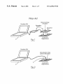
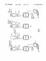
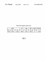
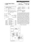
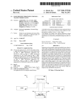
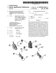
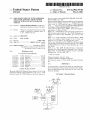
US006230119B1
(12) United States Patent
(10) Patent N0.:
(45) Date of Patent:
Mitchell
http://WWW.mot.com/pub/SPS/DSP/LIBRARY/56100/FMi
(54) INTEGRATED CIRCUIT WITH EMBEDDED
EMULATOR AND EMULATION SYSTEM
FOR USE WITH SUCH AN INTEGRATED
CIRCUIT
REVO/10.PDF, Oct. 1996*
Motorola Digital Signal Processor Application Development
System User’s Manual, Sections 1—5 [online], Motorola
Corp., Aug. 13, 1997 [retrieved Aug. 9, 1999]. Retrieved
from
http://WWW.mot.com/pub/SPS/DSP/LIBRARY/
TOOLSDOC/ADS/DSPADSUMPDF, Aug. 1997.*
“Ikos Grabs Emulation Firm, VMW”, Electronic Engineer
ing Times, p. 1, Mar. 18, 1996.*
(76) Inventor: Patrick Michael Mitchell, Carrigeeval,
Ballyvalley, Killaloe, County Clare (IE)
(*)
Notice:
Subject to any disclaimer, the term of this
patent is extended or adjusted under 35
Babb et al., “Virtual Wires: Overcoming Pin Limitations in
FPGA—based Logic Emulators”, Proc. IEEE Workshop on
FPGAs for Custom Comp. Machines, pp. 142—151, Apr.
USC 154(b) by 0 days.
(21) Appl. No.: 09/019,789
(22) Filed:
1993*
Babb et al., “Logic Emulation With Virtual Wires”, IEEE
Trans. on Computer—Aided Design of Int. Circuits and
Systems, vol. 16, Issue 6, pp. 609—626, Jun. 1997.*
Dahl et al., “Emulation of the SPARCLE Microprocessor
With the MIT Vritual Wires Emulation System”, Proc. IEEE
Workshop FPGAs for Custom Comp. Machines, pp. 14—22,
Apr. 1994.*
Feb. 6, 1998
(51)
Int. Cl.7 .................................................... .. G06F 9/455
(52)
US. Cl. ............................... .. 703/27; 703/28; 714/30;
(58)
Field of Search ....................... .. 395/500.44, 500.48,
714/35
395/500.49, 183.06, 183.01; 703/23—25,
28; 203/25; 710/7; 714/30, 33—35
(56)
US 6,230,119 B1
May 8,2001
Babb et al., “The RAW Benchmark Suite: Comuatation
Structures for General Purpose Computing”, Proc. 5th Ann.
IEEE Symp. on Field—PRogrammable Custom Computing
Machines, pp. 134—143, Apr. 1997.*
References Cited
U.S. PATENT DOCUMENTS
* cited by examiner
4,272,760 *
6/1981
PraZak et al. ...................... .. 341/120
PaWloski
5,313,618
*
5/1994
5,375,228
*
12/1994
.......
Leary et al.
. . . . ..
703/28
. . . ..
714/33
......
5,467,200 * 11/1995 Ohsawa et al.
5,488,688 *
5,752,077 *
5,758,059
Primary Examiner—Kevin J. Teska
Assistant Examiner—Douglas W. Sergent
(74) Attorney, Agent, or Firm—Wolf, Green?eld & Sacks,
358/426
1/1996 Gonzales et al. .
5/1998 Yiu et a1. ........ ..
.. 714/34
710/7
*
5/1998
Alexander
5,872,954 *
2/1999
Matsushita
.....
. . . . ..
5,898,862 *
4/1999
Vajapey ................................ .. 703/28
PC.
(57)
714/30
ABSTRACT
.... .. 703/23
A data processor is provided in Which an embedded emu
lator communicates With a control emulation system using a
OTHER PUBLICATIONS
serial communications link involving one pin of the data
processor package.
Motorola DSP56100 Technical Data, Section 10, On—Chip
Emulation (OnCE) [online], Motorola Corp., Oct. 7, 1996
[retrieved Aug. 10, 1999]. Retrieved from the internet at
30 Claims, 7 Drawing Sheets
Program
Memory
52
lnstructlon
Decoder
EA
Step
Break
Pin single points
Interrupt
Emulation
Request
Req uest
Next
Program
Program
V Address
Address
Controller
2K8 Boot
EEPROM
8KB Code
Flash
EEPROM
54
t
EMU REG
j
5b
U.S. Patent
May 8,2001
Sheet 1 0f 7
US 6,230,119 B1
Prior Art
Microcontroller
Emulator
Emulator GUI
Emuloting
System
l
\
Ergwslotion
17
Customer's
2
Fig 1
Target Board
Emulator GUI
Some Build in Chip
used for Emulotion
Customer's
Target Board
U.S. Patent
May 8,2001
Emma"
Sheet 2 0f 7
US 6,230,119 B1
NB User Does Not
During Emulation Requests
see lnternol Emulotion
The Internal Emulation
Memory
Memory is Activated
<- F900
[\,,\|2K l\ § <- F900
User _)
Mode Q:
Interface
Q:
Q:
Q" \~
Internal
tFFF
1'’ '-l
:\\‘/
H- I ‘
User _> VIE-Tr J
Mode
‘
Emulotor GUI
lFFF
5%,’
L: '_‘_I.
Interface
Q
;‘_'l I
0000
‘
0000
42
40
\/
tttt
30
/
EA Step
Pin Single Breokpoints
ln'fel'up’f
R
est
t t V43
Emulotion
Re est
eq“
qu
;|'
./
32
/ 24
2KB BOOT
Next
Program
Program —> Address
Address
2o
/
EEPROM
Controller
22
r
8K5 Code
Flosh
f EEPROM
28
Fig. 4
/
20
U.S. Patent
May 8,2001
Sheet 3 0f 7
US 6,230,119 B1
53
Program
5211
/
l
nrr Tin
lsuco
Decoder
EA
S’rep
Break
Pin single poin’rs
'merrupl
Request
Emula’rion
Request
2KB Boor
EEPROM
Nex’r
Program
Program —) Address
Address
J 32
Con’rroller
8K5 Code‘
Flash
EEPROM
ALU
1
EMU REG
Fig. 5
r 56
50
_/
U.S. Patent
May 8,2001
Sheet 6 0f 7
US 6,230,119 B1
EMUCON Register (EMUCON)
CLKD
0
R/W
EE
EES
ESS
EAIN
EAOUT
O
O
1
0
0
O
1
R/W
R/W
R/W
R/W
R/W
R
R/W
U.S. Patent
May 8,2001
Sheet 7 0f 7
US 6,230,119 B1
lI-.
Galvanic Isolo?on
gvcc
COM MS
IGND
TARGET
DATA PROCESSOR
Fig. 9
US 6,230,119 B1
1
2
INTEGRATED CIRCUIT WITH EMBEDDED
EMULATOR AND EMULATION SYSTEM
FOR USE WITH SUCH AN INTEGRATED
CIRCUIT
troller for causing the data processor to enter an emulation
mode, and dedicated registers for use in the emulation mode.
It is thus possible to provide a softWare driven emulator
Within a data processor Which leaves the registers used by
the data processor to execute tasks unaltered during an
TECHNICAL FIELD
The present invention relates to an integrated circuit
having an emulator embedded therein, and to an emulation
system for use With such an integrated circuit.
10
BACKGROUND OF THE INVENTION
Executable code for a data processor such as a
microcontroller, requires testing and correction during its
development cycle. SoftWare debugging is initially done in
15
a simulator or debugger offline. Once the softWare is
debugged, it is then doWn loaded into the target system.
HoWever, if the softWare does not Work correctly, for
example, due to a timing problem it is then necessary to do
or other information such as the contents of a stack or
memory can be output after executing a single instruction of
the user’s programme. Additionally or alternatively, the
emulation controller is responsive to a single byte instruc
tion placed in the user code in order to initiate the emulation
it is manipulating. It is knoWn to perform this be removing
the target data processor and replacing it With a replica of the
data processor Which can be probed or interrogated via an
emulation pod. The replica data processor emulates the real
tion
a reserved non-volatile memory area Which is hidden from
the use of the data processor.
Preferably the emulation controller can operate in a single
step mode Wherein the register status of the data processor,
an “in circuit” examination of the softWare and the data that
data processor and this process is called “in circuit emula
emulation or debug operation. A softWare driven emulator is
?exible and alloWs, for practical purposes, for an unlimited
number of break points to be implemented.
Preferably the registers dedicated for use by a data pro
cessing core (also knoWn as an arithmetic logic unit) of the
data processor during emulation can only be altered during
emulation.
Advantageously a programme for controlling the opera
tion of the data processing core during emulation is stored in
25
.
Adisadvantage of knoWn “in circuit” emulators is that the
additional sockets, clips, adaptors or pods can induce extra
parasitic components into the target system Which alter its
performance. This usually restricts the emulation to a sloW
mode. The single byte instruction is, in general Written over
another instruction in the user’s programme. In order to
ensure that the user’s program performs as intended, the
overWritten instruction is held in a special purpose register
so that it is executed When the emulation mode is excited.
Additionally or alternatively, the data processor may also be
responsive to a signal on one of the data processor control
speed in order to avoid timing problems introduced by the
parasitic components. The use of such in circuit emulators
can cause problems Where debugging is to be performed in
hybrid digital-analogue systems Where analogue accuracy is
a critical issue, especially When more than 6 or 7 bit 35
resolution of analogue variables is used.
It Was also knoWn, in the case of microcontrollers Where
the internal address and data busses do not come out to the
pins in order to initiate the emulation mode.
According to a second aspect of the present invention,
there is provided a data processor having an emulator
embedded therein, and in Which the emulator is initiated by
a single Work instruction.
According to a further aspect of the present invention,
there is provided a data processor including an emulator
therein arranged to communicate information concerning
pins of the data processor, to produce a special “bond-out”
the internal status of the data processor via a serial commu
version of the circuit. This has to be manufactured into a
nication link.
Preferably the serial data link utilises a pin in the data
bigger package to bring these extra signals to the pins so that
the emulator can monitor them. The bond-out version is
processor package. Advantageously the pin is multiplexed
disadvantageous since it requires the chip manufacturer to
create a second version of the chip and package, With
consequent timing differences from the read chip, increases
45
complexity, and a need to provide an adaptor for connecting
the “bond-out” version of the chip to target systems in place
is to initially execute instructions from an internal or an
of the standard chip package.
external memory. Once this information has been conveyed
to the processing core of the data processor the pin becomes
effectively redundant. Such a pin may then be used as a
communication link betWeen the embedded emulation sys
tem Within the data processor and an external development
It is knoWn to integrate emulation address comparators
and emulation break point registers Within an integrated
circuit and then to perform a hardWare compare of the
contents of the address resister With the emulation break
point register in order to determine When to force a break
point for emulation purposes. HoWever, the additional reg
system or emulator controller.
55
isters and comparators are Wasteful of space on the silicon
die of the integrated circuit, and are in?exible in their
operation. An additional register and comparator is required
for each break point. Typically a designer may Wish to have
betWeen eight and sixteen break points available. The addi
tion of sixteen or so additional registers and comparators can
add a signi?cant cost to the production cost of the integrated
circuit.
SUMMARY OF THE INVENTION
According to a ?rst aspect of the present invention, there
is provided a data processor including an emulation con
With a control function of the data processor. For example,
some data processors include control pins Which are only
relevant during the poWer up initialisation of the data
processor. The pin may indicate to the processor Whether it
Preferably the emulator is responsive to a signal on the
pin, such as a voltage transition, in order to activate the
emulator.
Preferably the emulator is a softWare controlled emulator,
and comprises emulation instructions held as softWare
Within a reserved memory integrated into the data processor.
The receipt of the instruction to start emulation, either by a
signal on the emulator control pin or via a softWare instruc
tion Within the softWare being debugged, forces the data
65
processing core of the data processor to suspend execution
of the user’s programming code and to execute instructions
from the emulation instruction code. Preferably the receipt
of an instruction to commence emulation causes a high level
US 6,230,119 B1
3
4
non maskable interrupt to be issued to the data processing
BRIEF DESCRIPTION OF THE DRAWINGS
core of the data processor.
The present invention Will further be described, by Way of
example, With reference to the accompanying draWings, in
Preferably the data processor executes emulation instruc
tions using reserved emulation registers, thereby leaving the
unaltered, except possibly for the programmed address con
Which:
FIG. 1 schematically illustrates a prior art emulator
troller and the stack Which may experience some minor and
arrangement;
Wholly reversible alterations. Advantageously an auxiliary
FIG. 2 schematically illustrates an emulator constituting
an embodiment of the present invention;
FIGS. 3a and 3b schematically illustrate the memory
organisation Within a data processor constituting an embodi
ment of the present invention in normal operation and in
contents of the registers used for programme code execution
stack and/or auxiliary programme address counters may also
be provided solely for use Within the emulation routine such
that the registers, programme counter and stack used by user
executable code may be left entirely unaltered. As an alter
10
native dedicated registers may also be provided for storing
emulation mode, respectively;
the contents of the program address controller In yet a
further alternative, the data processor may be arranged to
doWn load the stack and register contents to virtual registers
15
FIG. 4 schematically illustrates the internal layout of a
microcontroller constituting an embodiment of the present
With an emulator control data processor or Within an inter
invention;
face element, and to up load the register and stack contents
When exiting the emulation mode.
According to a further aspect of the present invention,
there is provided a development system comprising a control
data processor for monitoring the status of a target data
FIG. 5 schematically illustrates the internal layout of a
microcontroller constituting a further embodiment of the
present invention;
FIG. 6a to 6d schematically an emulation in a single step
mode;
processor, Wherein the target data processor includes an
embedded emulator for communicating information con
cerning the internal status of the target data processor via a
serial communications link, the development system includ
ing interface element adapted to communicate via the serial
FIG. 7 schematically illustrates an emulation using a
single step break point instruction;
25
FIG. 8 shoWs a layout of a special purpose emulation
register; and
communications link.
The interface element may be in the form of a pod
FIG. 9 schematically illustrates the emulation system.
providing electrical isolation betWeen the target and control
DESCRIPTION OF THE PREFERRED
EMBODIMENT
data processor. Advantageously the pod provides
bi-directional communication betWeen the target and control
data processors and includes a controllable voltage generator
for causing a voltage transient on an emulation control pin
of the target data processor for forcing it to enter the
emulation mode. The voltage generator may also be used to
communicate data and instructions to the target data pro
FIG. 1 schematically illustrates a prior art emulator in
Which a large emulation pod plugs into the data processor
35
package Which typically displays register contents of the
cessor.
target processor and alloWs for editing of instructions via a
graphical user interface (GUI). The large siZe of the emu
lation pod makes it inconvenient to use and also can give rise
to subtle changes in operation of the target board due to the
extra load and parasitic components introduced by the
emulation pod. Furthermore, the knoWn emulation pod uses
Advantageously the interface element communicates With
the control data processor via a conductive link, such as a
cable. Alternatively, the communications pod may commu
nicate With the control data processor over a radio or optical
based, such as infra-red, communications link. Advanta
geously the or each communications pod has a unique
identity such that a plurality of pods may be independently
addressed by a single emulation control data processor. Thus
a different or modi?ed data processor Which gives rise to
45
the emulation control data processor can control and/or
As shoWn in FIG. 2, an emulation system comprising a
system.
data processor constituting and embodiment of the present
invention and an interface card 3 for providing galvanic
Advantageously the or each interface element contains a
local data processor for handling may timing features or
handshaking required to communicate over the data link.
The local data processor may contain registers or memory
for temporarily storing the register contents of an associated
isolation betWeen the customer’s target board and the emu
lation control data processor 2 provides for a more compact
target data processor, or may handle the modi?cation of a 55
block user program code, i.e. changing the code or inserting
a break point instruction.
In a preferred embodiment, the or each interface element
is a pod having three pins, one for connection to ground, one
for connection to the poWer rail Vcc, and one for connection
to the pin on the target data processor for communication
thereWith.
emulation system and, more importantly does not change the
operating characteristics of the customer’s target board due
to the introduction of parasitic components.
The data processor having an emulator according to the
present invention performs emulation under softWare con
trol. In order to achieve this a reserved memory containing
emulation instructions is provided as an integral part of the
data processor. As shoWn in FIG. 3a, a data processor may
have, for example, a memory space in Which addresses
0000H to lFFFH (Where “H” indicates that the addresses are
expressed in hexadecimal) are provided for internal user
It is thus possible to integrate emulation and debug
As used herein, “emulation” includes softWare debugging
carried out using the target processor.
changes in output driving characteristics and loadings Which
can effect signal timings and degrade analogue performance
Where analogue circuits or DAC or ADC’s are involved.
debug a plurality of target data processors Within a target
features With a data processor, thereby ensuring that emu
lation has minimal effect on the operation of the target board.
socket on a customer’s target board in order to provide
interconnection With an emulator system comprising an
emulation control processor running an emulator softWare
65
programme code and the addresses 2000H to FFFFH are
allocated to external user code space. The emulation
memory is placed on another page of memory such that it
remains hidden from the user. Thus, for example, external
US 6,230,119 B1
5
6
memory addresses F900H to FFFFH may contain a user
programme, Whereas internal addresses F900H and above
contain the emulation programme.
processor to be disabled if the correct code, in this example
101, is Written into these bits of this function register. This
enables the emulator to halt internal timers and interrupts
FIG. 4 schematically illustrates the internal arrangement
When executing an emulation function. The fourth bit is an
emulation enable bit, EE, Which is placed in the enable
of a data processor, generally illustrated as 20, Whereby a
programme address controller 22 holds the address of the
condition by default and enables emulation to be started
When an appropriate emulation request is received by the
emulation request controller. The ?fth bit enables execution
of the contents of the special function register EMU2. When
next memory location to be read from. This location nor
mally points to a boot strap memory 24 Which contains
executable code to be used during poWer up sequences or for
data exchange routines, or to a user programme 26 Which
may be stored in an internal user code memory 28 or in
10
external memory (not shoWn). The programme address
controller 22 is responsive to an interrupt request handler 30
Which, as is Well knoWn in the art, alloWs normal execution
of a programme to be interrupted in order to respond in a
15
an emulation routine is started by the occurrence of the
emulation break point in the user programme code, this EES
register is inspected in order to determine Whether the break
point instruction should actually be executed. If the contents
of this register are not set, then the emulation Will be
performed. When the emulation routine is completed, the
address pointer points to the address of the break point. As
predetermined Way to speci?c events. The data processor is
mentioned earlier, the original instruction Which Was over
arranged to execute an interrupt routine in response to an
interrupt request and then to return to the user code When the
Written by the break point is loaded into the EMU2 special
interrupt routine has been completed. The data processor
programme returns control to user code, it sets the EES bit.
The address programme counter Will return control at the
function register and the bit EES is cleared. As the emulation
constituting an embodiment of the present invention is also
provided With an emulation request controller 32 Which
issues a priority non-maskable interrupt request Which takes
precedence over all other interrupt functions. The interrupt
controller 30 is arranged to buffer incoming interrupts While
the programme address controller is responsive to the emu
lation request controller 32 in order to ensure that interrupt
requests are properly serviced upon return from the emula
tion mode.
25
the EMU2 register is executed, thereby ensuring that the
next occurrence of the break point instruction Will cause the
emulation routine to be re-entered.
The sixth bit is an emulation single step, ESS bit Which
causes the data processor to only execute single instructions
The emulation request controller is responsive to three
inputs. A ?rst input 40 is responsive to a voltage transition
on a single pin of the data processor package. In the
preferred embodiment, the pin is a “EA” pin (provided on all
ADuC812 data processor) Which is used to tell the data
betWeen emulator programme operations.
The ?nal tWo bits EA-in and EA-out enable the status of
processor and it should execute from internal (EA=high) or
external (EA=loW) memory during the poWer up. The state
of the pin is latched by the data processor at poWer up or
address of the break point instruction. HoWever, this time the
EES bit is set and instead of re-executing the emulation
routine, the processing core of the data processor is caused
to execute the instruction held in the EMU2 special function
register. The EES bit is then toggled once the instruction in
35
the EA pint to be read and Written to respectively.
FIGS. 6a to 6d schematically illustrate operation of the
emulator in a single step code execution mode. The emula
tion routine takes advantage of the fact that the emulation
interrupt Will not respond until at least one instruction of the
reset and thereafter it can be used as the emulation control
user code has been executed. Thus once control has been
pin. The EA pin is also used, When emulation has been
passed from the emulator to the user code, the emulator
issues, via a hardWare resource, a highest priority non
maskable interrupt that ensures that programme execution is
initiated, as a bi-directional serial communications pin.
The emulation request controller is also responsive to a
single step ?ag 42 Which ensures that an emulation request
immediately returned to the emulator, irrespective of What
instruction Was being performed.
occurs after execution of a single instruction of the user
programme code. Preferably, the emulation controller 32 is
responsive to a break point instruction 43 Whose occurrence
in the user code causes the emulation controller 32 to issue
an emulation request.
45
Thus as shoWn in FIG. 6a, the emulation control data
processor is arranged to issue an emulation request via the
EA pin Which causes a jump to the emulation memory. This
initially alloWs communication betWeen the emulation con
trol data processor 2 and the emulator in order that neW
As shoWn in FIG. 5, a break point instruction decoder 50
is provided to speci?cally handle the occurrence of the
instructions can be set in the emulator, such as changing one
additional single byte emulation instruction (break point
example, the control data processor sets the single step
instruction, ESS, ?ag in the EMUCON register. Once the
or more of the ?ags in the EMUCON register, in this
instruction) contained Within user programme memory 52,
Which may be external memory or, more likely, internal
memory area 28. Additionally, a special register EMU2 53
is provided to hold the instruction Which Was overWritten by
the emulation request instruction thereby ensuring that the
55
addresses of the remaining programme code are unaltered.
As shoWn in FIG. 5, the processing core 54 (also knoWn as
an arithmetic logic unit ALU) has a dedicated set of reserved
With the single step enabled, and interrupt request is issued
via the emulation controller 32 thereby causing control to be
registers 56, EMUCON, EMUl and EMU2, for using during
emulation. The reserved register set may also include an
alternative stack and/or programme counter for use during
emulation.
FIG. 8 illustrates the emulation control register,
EMUCON, provided Within a data processor including an
embedded softWare controlled emulator. Workings from the
left to right, the ?rst three bits of the register form a control
Word Which causes internal timers and clocks of the data
emulation control data processor has indicated that it does
not Wish to set any further instruction changes, control is
relinquished from the emulation code and the user code is
executed. HoWever, since the EMUCON register Was set
65
returned to the emulation code after a single instruction of
the user code has been executed as shoWn in FIG. 6c. The
emulation code then doWn loads data to the emulation
control data processor 2 via the EA pin. DoWn loaded data
may include the status of the internal registers of the data
processor, but may also, depending on instructions received
from the emulation control data processor, include the
contents of the stack and also the contents of selected areas
internal or external memory, or the contents of an internal
cache.
US 6,230,119 B1
8
7
FIG. 7 illustrates an example of an emulation request
the data has been sent to the emulation data processor, the
emulation data processor toggles the EES bit and issues a
initiated via the break point instruction.
command causing the emulation to continue. The emulator
The data processor has a data processing core supporting
the 8051 instruction set. The 8051 instruction set has a
then returns control to the user programme. Because the
unused instruction code of A5. The A5 instruction has been
break point instruction is interrupt driven, the control is
implemented as the break point instruction.
returned to address 0120 Which holds the A5 break point
instruction. This time the EES bit indicates that emulation
should not be recommenced, but in fact that the instruction
in the EMU2 register should be executed. The data process
ing core executes the instruction in the EMU2 register and
It is knoWn to initiate a softWare emulation or debug by
including a jump instruction to the emulation code. HoWever
there is a signi?cant problem With this approach since the
jump instruction is a 3 byte instruction and if this Was
inserted at address 0120, as shoWn in FIG. 7 then the inc A
and DAA instructions at addresses 0121 and 0122,
10
returns control to the user programme at the address fol
loWing the break point instruction.
FIG. 9 schematically illustrates a multi-target develop
respectively, Would be overWritten by the jump instruction.
Thus it Would be necessary to change the addresses of the
subsequent steps in order to incorporate the addition of this
jump driven emulation instruction. Secondly, in order to use
this approach, the emulation memory/programme must be
visible for the jump to Work and consequently the incorpo
15
ration of the emulation code Within the data processor Would
limit the user’s programming options. A third problem is
20
that, if the addresses of all the remaining code Was not
changed, it Would result in the instructions at 0121 and 0122
being lost, and also an additional break point could not be
inserted at the overWritten addresses.
By adding a single byte break point instruction, only one
ment system in Which a single control data processor 2
communicates With a plurality of target data processors via
a plurality of interface elements 3, each of Which contain a
local data processor 100 Which reduces the computational
load on the control data processor by performing the com
munications protocols and also buffers and modi?ed data in
the target data processors in response to commands from the
emulation control data processor 2.
It is thus possible to provide a data processor having a
softWare driven emulator embedded therein Which uses
25
dedicated registers, thereby ensuring that registers used in
execution of a user’s programme do not become altered once
address of programme is over Written. Thus in the example
in FIG. 7 only the “clear A” instruction at 0120 is overWrit
ten by the inclusion of the softWare driven emulation break
the emulation mode is commenced. It is also possible to
provide a development system for use With such a micro
as if the break point instruction Were not there. If a break
processor in order that the internal registers may be
inspected, or blocks of memory may be inspected and
analysis performed thereon. For example, a block of
point instruction is to be Written into the user code for
debugging/development purposes, the emulator reads out a
memory may hold values resulting from analogue to digital
conversions. The values may be displayed by the emulation
point instruction. HoWever, the clear A instruction is Written
into the EMU2 register in order to ensure that it is executed
30
control data processor in order to form an oscilloscope trace
block of memory containing the program code containing
the address of the instruction to be changed. An internal
35
memory controller then erases the block of memory, and in
co-operation With the emulation control data processor,
re-programs the block of memory adding the break point
instruction. The precise memory control strategies for per
forming the modi?cation of internal memory Within the data
processor, ie within a single chip package, are not critical
40
to the present invention, but a suitable memory and memory
controller is described Within a co-pending application ?led
by Analog Devices, and titled “A MEMORY AND A DATE
PROCESSOR INCLUDING A MEMORY”. The interface
element 3 may provide a local buffer such that as the block
45
The emulator has authority to modify the internal memory
re-programmed Whilst it is in situ in the target board.
Similarly calibration coef?cients in digital or hybrid digital
55
analogue systems can be modi?ed. It is also possible, When
the interface element communicates using a radiative link, to
leave the interface element attached to the target board
permanently, thereby alloWing for the target data processor
to be re-programmed even after it has been installed in a
Working environment. The provision of an emulator as an
integral part of the target data processor has the additional
60
advantage that the board and processor being debugged/
developed are identical to the ?nal system. This contrasts
EES bit is cleared, the data processing core executes the
and outputs data concerning the status of the various pro
gramme registers to the emulation data processor 2. Once
emulator 2 may display a plurality of WindoWs, With each
displaying the status of and/or controlling the function of a
respective target data processor Within a multi-processor
target board. Thus the operation of master and slave pro
cessors may be analysed, possibly on a single step basis, in
order to check their data exchange operations and mutual
contents of program and data memory Within the target data
processor. Thus the target data processor may be
EES bit in the EMUCON register cleared. Assuming that the
emulation instructions using the reserved EMU1 register,
send these to the emulator control processor Which can then
display a graph or trace of the converted variable. The
performance.
of program code (usually tWo roWs on the internal non
volatile reprogrammable user code memory of the data
processor), is buffered in the interface element and the local
data processor modi?es the data to change instructions or
insert the break point, and then re-presents the data to the
target data processor in order that it can reWrite the data into
in’s internal memory.
During execution of the user programme, the programme
counter Will eventually point to the address 0120 Which has
the A5 emulation break point instruction Written therein in
place of the “clear A” instruction. The instruction decoder of
the data processor decodes the break point instruction and
causes the emulation request controller 32 to issue a priority
interrupt. Thus the data processing core 54 discontinues
execution of the user’s programme and starts executing
instructions from the emulation memory provided that the
of the analogue value, or additionally or alternatively may be
Fourier transformed in order to perform frequency domain
analysis. The emulator may be used to perform a softWare
controlled series of Analogue to Digital conversion, and to
65
With prior art emulators of the type shoWn in FIG. 1 Whereby
the data processor on the emulation pod synthesises the
functions of the target data processor but in often a physi
cally different type of processor Which may have additional
hardWare attached thereto to simulate the ports of the target
data processor.
US 6,230,119 B1
9
10
What is claimed is:
1. A data processor including an emulator, wherein the
16. A development system as claimed in claim 4, in Which
the interface element automatically detects the data trans
mission rate of an associated target data processor operating
emulator is arranged to perform bi-directional communica
tion With an external development system via only a single
terminal.
in an emulation mode.
2. A data processor as claimed in claim 1, in Which said
single terminal is a control pin of said data processor, said
the interface element performs handshaking and data
eXchange With the target data processor.
17. A development system as claimed in claim 4, in Which
pin only controlling said data processor during a predeter
mined operation.
3. A data processor as claimed in claim 2, in Which said
18. A development system as claimed in claim 4, in Which
10
predetermined operation is an initialisation sequence.
4. A development system for use With a target data
processor including an emulator, Wherein bi-directional
communication betWeen said development system and the
target data processor occurs via a serial data link utilising
the interface element performs handshaking and data
eXchange With the control data processor.
19. A development system as claimed in claim 4, in Which
the interface element moves control and data information
15
only a single pin of the data processor, said development
betWeen the target and control data processors.
20. A development system as claimed in claim 4, in Which
the interface element communicates With the target data
processor via a serial communications link.
system comprising a control data processor and at least on
interface element each providing an interface betWeen the
control data processor and a respective target data processor.
21. A development system as claimed in claim 4, and
arranged to communicate With a target data processor such
that a program code stored in an EEPROM of the target data
processor can be programmed in situ.
22. A development system as claimed in claim 4, in Which
5. A development system as claimed in claim 4, in Which
said at least one interface element provides electrical isola
tion betWeen the target data processor and the control data
processor.
the development system can modify programme instructions
stored in an EEPROM Within the target data processor and
6. A development system as claimed in claim 4, in Which
the at least one interface element contains means for causing 25 also modify data.
23. A development system as claimed in claim 22,
a transition on the data link in order to cause the target data
Wherein said data includes calibration coef?cients.
24. A development system as claimed in claim 4, Wherein
processor to enter an emulation mode.
7. A development system as claimed in claim 6, in Which
said transition causing means is controllable to transmit
instructions to the target data processor.
the development system interfaces simultaneously With a
plurality of target data processors.
25. A development system as claimed in claim 4, Wherein
the development system is arranged to retrieve data from at
8. A development system as claimed in claim 4, further
comprising a plurality of interface elements, Wherein each
interface element is individually addressable by the control
least one target data processor and display the data in a
graphical form.
data processor.
9. A development system as claimed in claim 4, Wherein
35
bi-directional communication betWeen the at least one inter
face element and the control data processor is via a radiative
data link.
10. Adevelopment system as claimed in claim 9, in Which
the radiative data link is an infra-red data link.
11. Adevelopment system as claimed in claim 4, Wherein
the status and register contents of the registers of the target
domain analysis of the data said target data processor being
data processor used for program code execution are
retrieved and stored during emulation.
12. A development system as claimed in claim 11,
Wherein the status and register contents of the target data
45
data processor occurs via a serial data link utilising a only
single pin of the target data processor.
13. A development system as claimed in claim 11,
Wherein the status and register contents of the target data
29. A development system as claimed in claim 4, in Which
the interface member is left permanently connected to the
target data processor and communicates With the control
processor are stored in an associated interface element.
14. A development system as claimed in claim 4, Wherein
the development system is arranged to read a block of
data processor via a radiative communications link.
30. An interface member as claimed in claim 28, in Which
program code from an area of EEPROM Within the data
break point instruction at a chosen location so as to over
Write an instruction in the program code Without changing
the length of the program code.
a production version of the data processor and not a special
emulation version.
28. An interface member for performing serial commu
nication With a target data processor and for communicating
With an emulation control data processor, said target data
processor including an emulator, Wherein bi-directional
communication betWeen said development system and the
processor are returned to the target data processor before
recommencing eXecution of a user program.
processor, to modify the program code and to re-present the
modi?ed code to the EEPROM of the target data processor.
15. A development system as claimed in claim 14, in
Which the program code is modi?ed by the insertion of a
26. A development system as claimed in claim 25, Where
in graphical form is an oscilloscope trace.
27. A development system as claimed in claim 4, Wherein
the development system is arranged to retrieve data from the
at least one target data processor and to perform frequency
55
the interface member includes local memory such that the
interface member can read a block of program code form
EEPROM of the target data processor, modify the contents
of the block of program code and reWrite it to the target data
processor.