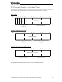
1
G7 Adjustable
Speed Drive
Multi-Protocol
Communication
And PG Feedback
Option Manual
Document Number: ICC-10389-003-V3.00
Date: August 2002
About This Manual
This manual was written by the TOSHIBA Technical Publications Group. This group is tasked with
providing technical documentation for the G7 Adjustable Speed Drive. Every effort has been made to
provide accurate and concise information to you, our customer.
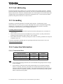
Contacting TOSHIBA’s Customer Support Center
TOSHIBA’s Customer Support Center can be contacted to obtain help in resolving any G7 Adjustable
Speed Drive system problem that you may experience or to provide application information. The
center is open from 8 a.m. to 5 p.m. (CST), Monday through Friday. The Support Center’s toll free
number is US (800) 231-1412/Fax (713) 466-8773 — Canada (800) 527-1204.
You may also contact TOSHIBA by writing to:
TOSHIBA International Corporation
13131 West Little York Road
Houston, Texas 77041-9990
Attn: ASD Product Manager.
For further information on TOSHIBA’s products and services, please visit our website at
TIC.TOSHIBA.COM.
TOSHIBA is a registered trademark of the TOSHIBA Corporation.
All other product or trade references appearing in this manual are registered trademarks of their
respective owners.
The information in this manual is subject to change without notice.
TOSHIBA International Corporation shall not be liable for technical or editorial omissions or mistakes
in this manual, nor shall it be liable for incidental or consequential damages resulting from the use of
information contained in this manual.
This manual is copyrighted. No part of this manual may be photocopied or reproduced in any form
without the prior written consent of TOSHIBA International Corporation.
© Copyright 2002 TOSHIBA International Corporation.
All rights reserved.
Printed in the U.S.A.
TOSHIBA INTERNATIONAL CORPORATION
G7 Adjustable Speed Drive Multi-Protocol and PG Feedback Option
Please complete the Warranty Card supplied with the option and return it to Toshiba by prepaid mail.
This will activate the 12-month warranty from the date of installation; but shall not exceed 18 months
from the date of purchase.
Complete the following information about the option and retain it for your records.
Model Number: ASD-MULTICOM-A or ASD-MULTICOM-B
Serial Number:
Date of Installation:
Inspected By:
Name of Application:
Important Notice
This user manual may not cover all of the variations of option applications, nor may it provide
information on every possible contingency concerning installation, programming, operation, or
maintenance.
The contents of this user manual shall not become a part of or modify any prior agreement,
commitment, or relationship between the customer and TOSHIBA International Corporation.
The sales contract contains the entire obligation of TOSHIBA International Corporation. The
warranty contained in the contract between the parties is the sole warranty of TOSHIBA
International Corporation’s ASD Division and any statements contained herein do not create
new warranties or modify the existing warranty.
Any electrical or mechanical modifications to this equipment without prior written consent of
TOSHIBA International Corporation will void all warranties and may void any UL/CUL listing
or other safety certifications. Unauthorized modifications may also result in equipment damage
or personal injury.
This Manual’s Purpose and Scope
Currently, this manual covers the following G7 Adjustable Speed Drive options:
•
ASD-MULTICOM-A (multi-protocol communications + PG feedback)
•
ASD-MULTICOM-B (PG feedback only)
Not all sections of this manual will apply to the ASD-MULTICOM-B option. These sections
will be indicated in their respective introduction paragraphs.
This manual provides information that will assist the qualified user in the safe installation,
setup, operation, and disposal of the G7 Adjustable Speed Drive Multi-Protocol
Communication Option and PG Feedback Option. The information provided in this manual
is applicable to the G7 Adjustable Speed Drive Multi-Protocol Communication Option and
PG Feedback Option only.
This operation manual provides information on the various features and functions of these
powerful cost-saving devices, including
•
Installation,
•
System operation, and
•
Mechanical and electrical specifications.
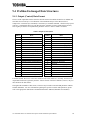
Table of Contents
1.
Introduction ........................................................................................................... 1
2.
Safety Precautions ................................................................................................. 2
2.1
2.2
2.3
2.4
2.5
Installation Precautions ................................................................................................................ 2
Maintenance Precautions.............................................................................................................. 3
Inspection ..................................................................................................................................... 3
Storage ......................................................................................................................................... 3
Disposal........................................................................................................................................ 3
3.
Board Overview..................................................................................................... 4
4.
Installation ............................................................................................................. 5
4.1
4.2
Installation Procedure................................................................................................................... 5
Wiring .......................................................................................................................................... 7
5.
Environmental Specifications............................................................................... 7
6.
PG Feedback Operation........................................................................................ 8
6.1
6.2
6.3
6.4
6.5
PG Feedback Enable Setting ........................................................................................................ 8
PG Power Supply Voltage Selection ............................................................................................ 8
Pulse Input Selection .................................................................................................................... 9
PG Feedback Connection ........................................................................................................... 10
Maximum Input Frequency Using an Open Collector Encoder.................................................. 13
7.
LED Indicators .................................................................................................... 14
8.
Network Configuration Parameters .................................................................. 15
8.1
8.2
8.3
9.
Profibus DP Configuration ......................................................................................................... 16
Modbus RTU Configuration....................................................................................................... 17
DeviceNet Configuration............................................................................................................ 18
Profibus Interface................................................................................................ 19
9.1
Feature Summary........................................................................................................................ 19
9.2
Profibus Interface Connection.................................................................................................... 21
9.3
Unit Addressing.......................................................................................................................... 21
9.4
Profibus Exchanged Data Structures .......................................................................................... 22
9.4.1 Output (Control) Data Format .............................................................................................. 22
9.4.2 Input (Status) Data Format.................................................................................................... 25
9.5
Diagnostics ................................................................................................................................. 31
9.6
Asynchronous Drive Parameter Access...................................................................................... 32
9.6.1 Parameter Number / Action Output Words............................................................................ 32
9.6.2 Parameter Number / Action Input Words .............................................................................. 33
G7 ASD Multi-Protocol Communication Option and PG Feedback Option Manual
i
9.6.3 Drive Parameter Access Procedure .......................................................................................34
9.6.4 Register Access Error Codes..................................................................................................35
9.7
Parameters...................................................................................................................................35
10.
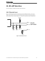
RS-485 Interface...............................................................................................36
10.1
Physical Layer.............................................................................................................................36
10.2
Modbus RTU ..............................................................................................................................37
10.2.1
Configuration .....................................................................................................................37
10.2.2
Communication Formats....................................................................................................37
10.2.3
Modbus/ASD Register Mappings .......................................................................................38
10.2.4
ASD Scan Registers............................................................................................................39
10.2.5
Supported Modbus Functions ............................................................................................41
10.2.6
Programmable Pointer Registers.......................................................................................42
10.2.7
Response Delay Timer Function ........................................................................................42
10.2.8
LED Indicators...................................................................................................................43
10.2.9
Register Summary ..............................................................................................................43
11.
DeviceNet Interface..........................................................................................45
11.1
Feature Summary ........................................................................................................................45
11.2
Unit Addressing ..........................................................................................................................46
11.3
Grounding ...................................................................................................................................46
11.4
Connection Information ..............................................................................................................46
11.4.1
Connection Sizes ................................................................................................................46
11.4.2
I/O Assembly Instances ......................................................................................................47
11.5
Object Specifications ..................................................................................................................48
11.5.1
Identity Object....................................................................................................................49
11.5.2
Message Router..................................................................................................................51
11.5.3
DeviceNet Object ...............................................................................................................52
11.5.4
Assembly Object.................................................................................................................54
11.5.5
Connection class ................................................................................................................58
11.5.6
Control Supervisor Object .................................................................................................62
11.5.7
Motor Data Object .............................................................................................................65
11.5.8
AC/DC Drive Object ..........................................................................................................67
11.5.9
Parameter Class.................................................................................................................72
11.6
Network Communication Loss Action ........................................................................................73
12.
Notes ..................................................................................................................75
G7 ASD Multi-Protocol Communication Option and PG Feedback Option Manual
ii
1. Introduction
Congratulations on the purchase of the new G7 Adjustable Speed Drive (ASD) Multi-Protocol
Communication (ASD-MULTICOM-A) or PG Feedback (ASD-MULTICOM-B) Option.
ASD-MULTICOM-A / ASD-MULTICOM-B
These option cards provide the ability to connect various different pulse generator/feedback sources,
such as encoders, to the G7 ASD. These PG input signals can then provide enhanced performance for
vector control, pulsed speed command, and process (PID) control applications.
Two different types of pulse input circuitry are provided, which allows very flexible application and
connectivity to a wide array of PG devices available on the market today.
ASD-MULTICOM-A
In addition to the PG feedback circuitry, this option card also provides connectivity to the most popular
fieldbus networks in use today. These networks include Profibus, DeviceNet, and RS-485 based
networks. Different option board firmware versions may provide varying levels of support for these
different networks, so when using this manual, always keep in mind that the firmware version operating
on your option board must match this manual’s respective revision for all documented aspects to apply.
The option board firmware version covered by each revision of the manual is indicated in the last
section of the “Document Number” on the manual’s front cover. For example, if the Document Number
on the front cover ends in “-V3.00”, then this manual is only applicable for version 3.00 option board
firmware.
The method of determining your board’s firmware version varies depending on the network being used.
Please refer to the specific network interface sections of this manual to determine the method required
for your installation.
This manual will primarily be concerned with the option’s hardware specifications, input characteristics,
configuration, and installation and wiring precautions. For more advanced application-level
information, please contact Toshiba’s ASD Marketing Department for copies of available application
notes.
To maximize the abilities of your new ASD option, a working familiarity with this manual will be
required. This manual has been prepared for the option installer, user, and maintenance personnel. With
this in mind, use this manual to develop a system familiarity before attempting to install or operate the
device.
G7 ASD Multi-Protocol Communication Option and PG Feedback Option Manual
1
2. Safety Precautions
Rotating shafts and electrical equipment can be hazardous. Installation, operation, and
maintenance of the ASD and option shall be performed by Qualified Personnel only.
Qualified Personnel shall be:
•
Familiar with the construction and function of the ASD and option, the equipment
being driven, and the hazards involved.
•
Trained and authorized to safely clear faults, ground and tag circuits, energize
and de-energize circuits in accordance with established safety practices.
•
Trained in the proper care and use of protective equipment in accordance with
established safety practices.
Installation of ASD systems and associated options should conform to the 1999
National Electrical Code Article 110 (NEC) (Requirements For Electrical
Installations), all regulations of the Occupational Safety and Health
Administration, and any other applicable national, regional, or industry codes and
standards.
DO NOT install, operate, perform maintenance, or dispose of this equipment until
you have read and understood all of the following product warnings and user
directions. Failure to do so may result in equipment damage, operator injury, or death.
2.1 Installation Precautions
•
Use lockout/tagout procedures on the branch circuit disconnect before installing
the option into the ASD.
•
Avoid installation in areas where vibration, heat, humidity, dust, metal particles,
or high levels of electrical noise (EMI) are present.
•
Do not install the ASD or option where it may be exposed to flammable
chemicals or gasses, water, solvents, or other fluids.
•
Where applicable, always ground the option appropriately to prevent electrical
shock to personnel and to help reduce electrical noise. The ASD’s input, output,
and control power cables are to be run separately from the option’s associated
cables.
Note: Conduit is not an acceptable ground.
•
Turn the power on only after attaching the front cover.
•
Follow all warnings and precautions and do not exceed equipment ratings.
•
The ASD maintains a residual charge for a while after turning the ASD off. Wait
at least ten minutes before servicing the ASD after turning the ASD power off.
Ensure that the Charge LED is off prior to beginning installation.
•
For further drive-specific precaution, safety and installation information, please
refer to the G7 Adjustable Speed Drive Operation Manual supplied with your
drive.
G7 ASD Multi-Protocol Communication Option and PG Feedback Option Manual
2
2.2 Maintenance Precautions
•
Use lockout/tagout procedures on the branch circuit disconnect before servicing
the ASD or installed option.
•
The ASD maintains a residual charge for a while after turning the ASD off. Wait
at least ten minutes before servicing the ASD after turning the ASD power off.
Ensure that the Charge LED is off.
•
Do Not attempt to disassemble, modify, or repair the option card. Call your
Toshiba sales representative for repair or service information.
•
Turn the power on only after attaching the front cover and Do Not remove the
front cover of the ASD when the power is on.
•
If the ASD should emit smoke or an unusual odor or sound, turn the power off
immediately.
•
The heat sink and the discharge resistors may become extremely hot to the touch.
Allow the unit to cool before coming in contact or performing service on the ASD
or option card.
•
The system should be inspected periodically for damaged or improperly
functioning parts, cleanliness, and to determine that the connectors are tightened
securely.
2.3 Inspection
Upon receipt, perform the following checks:
•
Inspect the unit for shipping damage.
•
Check for loose, broken, damaged or missing parts.
Report any discrepancies to your Toshiba sales representative.
2.4 Storage
•
Store the device in a well ventilated location (in its shipping carton, if possible).
•
Avoid storage locations of extreme temperatures, high humidity, dust, or metal particles.
2.5 Disposal
•
Contact the local or state environmental agency in your area for details on the disposal of
electrical components and packaging.
•
Do not dispose of the unit via incineration.
G7 ASD Multi-Protocol Communication Option and PG Feedback Option Manual
3
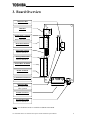
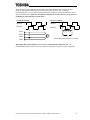
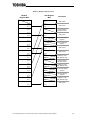
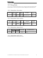
3. Board Overview
DIP Switch DS1
Refer to Sections 6.1 & 6.2
MMI Port
Reserved
Module Status / Network
Status LEDs
Refer to network sections
DeviceNet Connector
Refer to Section 11
Pulse Input Selection
Refer to Section 6.3
DATA_EXCHG LED
Refer to Section 9.1
PG Feedback Terminals
Refer to Section 6.4
RS-485 Terminals
Refer to Section 10
Control Board Connector
Refer to Section 4
DIP Switch DS3
Currently reserved: leave in
“OFF” position
Profibus Connector
Refer to Section 9
PG Circuit Ground
Refer to Section 6.4
NOTE: Not all indicated items are available on ASD-MULTICOM-B.
G7 ASD Multi-Protocol Communication Option and PG Feedback Option Manual
4
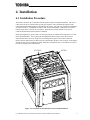
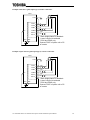
4. Installation
4.1 Installation Procedure
The interface cards for the G7 ASD have been designed for quick and simple installation. The card is
connected to the drive's control board via an 80-pin connector, and is mechanically supported with
nylon standoffs attached through the control PCB to the chassis. The only tools required for installation
are a flat screwdriver, a #2 Phillips screwdriver and, for most installations, a utility knife to aid in the
removal of the front cover's side access window. Each interface card kit includes one #51326A
connector PCB and four #47220 nylon hex standoffs.
Before opening the drive, please observe all safety precautions as outlined on the unit's front cover and
in the operation manual. After securing the unit against hazardous voltages, loosen the two lower
fasteners and remove the cover, taking care not to damage the keypad-to-drive cable connection.
Remove the four pan head screws that secure the control PCB to the drive (refer to Figure 1) and replace
with the #47220 1/2" hex standoffs provided. Make these substitutions one or two fasteners at a time to
prevent any shifting of the control board.
#51326A
#47220
#47220
Figure 1: Screw Removal, Standoff and Connector PCB Installation
G7 ASD Multi-Protocol Communication Option and PG Feedback Option Manual
5
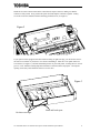
Install the #51326A connector PCB in the control board's 80-pin connector, making sure that the
connector is fully seated. Next, position the option card and snap the connectors together. Finally,
secure the card to the standoffs with the remaining pan head screws (see Figure 2).
Figure 2
If your option card is equipped with a data connector along its right side edge, you will need to remove
the side access window of your drive's cover before reinstalling it. Place the cover upside down on a
level surface (see Figure 3), and with downward pressure on your utility knife, cut along the two vertical
grooves. Next, bend the resulting flap back and forth several times until it snaps apart. Clean up the
opening as necessary and reattach the front cover to the drive.
Figure 3
Cut these two edges
Bend and break apart
G7 ASD Multi-Protocol Communication Option and PG Feedback Option Manual
6
4.2 Wiring
•
Use shielded wire for control signals and ground the unit with shielded wire.
•
Applicable wire size for terminal block TB1 is 0.2 to 2.5mm2.
•
Strip off the end of the wire by about 5mm.
•
For connecting wires, use a screwdriver that has a blade tip of 0.4mm thickness and 2.5mm width.
•
Tightening torque of the terminal block screws should be 0.22 to 0.25Nm.
•
Never route the signal or communication network lines and main circuit power wires
together. Separate the signal and communication network lines and the main circuit power wires
by more than 200mm.
•
Use 0.75mm2 wire for connecting the option’s PGCC terminal to the drive’s CC terminal.
•
Use 0.75mm2 wire for connecting the option’s ground lug (TB2) to the drive’s G/E terminal.
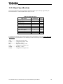
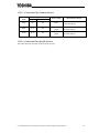
5. Environmental Specifications
Item
Operating Environment
Operating Temperature
Storage Temperature
Relative Humidity
Vibration
Cooling Method
Specification
Indoors, less than 1000m above sea level, do not expose to direct
sunlight or corrosive / explosive gasses
-10 ∼ +50°C (+14 ∼ +122°F)
-40 ∼ +85°C (-40 ∼ +185°F)
20% ∼ 90% (without condensation)
5.9m/s2 {0.6G} or less (10 ∼ 55Hz)
Self-cooled
G7 ASD Multi-Protocol Communication Option and PG Feedback Option Manual
7
6. PG Feedback Operation
This section applies to both ASD-MULTICOM-A and ASD-MULTICOM-B option boards.
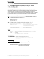
6.1 PG Feedback Enable Setting
To enable PG feedback with the option, set the position of switch #4 on DS1 to the ON position as
shown in the figure below.
Switch #4 for PG enable
PG disabled: set all switches to OFF
(default for ASD-MULTICOM-A).
CN3UB
DS1
ON
OFF
1
2
3
PG enabled: set switch #4 to ON
(default for ASD-MULTICOM-B).
4
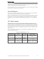
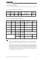
6.2 PG Power Supply Voltage Selection
The PG feedback option is capable of providing a PG power supply of 5V, 6V, 12V or 15V. To select
the desired PG power supply voltage, properly set the position of switch #1, switch #2, and switch #3 on
DS1 as shown in the figure below. Table 1 provides the proper switch settings.
CN3UB
DS1
ON
OFF
1
2
3
4
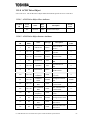
Table 1: PG Power Supply selection
Power Supply
Switch 1
Switch 2
Switch 3
5V
6V
12V
15V
OFF
ON
ON
ON
OFF
OFF
ON
ON
OFF
OFF
OFF
ON
G7 ASD Multi-Protocol Communication Option and PG Feedback Option Manual
8
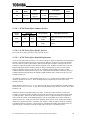
6.3 Pulse Input Selection
JP6
JP1
JP2
JP3
JP4
JP5
CN3UB
Two different types of pulse input circuitry are provided. To select the desired pulse input circuitry,
properly set the position of jumpers JP1~JP6 as shown in the figure below. Table 2 provides the proper
jumper settings.
Type 1 selected:
Line driver input
Type 2 selected:
Open collector input
Jumpers for Pulse Input selection
Table 2: Jumper Settings
Pulse Input Type
Characteristics
Rated voltage output with emitter/follower combination.
Higher noise-immunity characteristics.
High-speed response. Long-distance transmission capability.
Need to pay attention to waveform irregularity.
Input voltage (VPGA1-PGA2) range: 8.3V-16.6V
Input circuit diagram:
Type 1
Line Driver
G7 ASD Multi-Protocol Communication Option and PG Feedback Option Manual
9
Pulse Input Type
Characteristics
Lower noise-immunity characteristics.
Need to pay attention to waveform irregularity and distortion.
Input circuit diagram:
Type 2
Open Collector
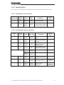
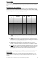
6.4 PG Feedback Connection
The pulse input signals are connected to terminal block TB1. Table 3 provides terminal descriptions for
terminal block TB1. PGA1 and PGA2 are connected for Phase A, PGB1 and PGB2 are connected for
Phase B, and PGZ1 and PGZ2 are connected for Phase Z. The wiring for Phase Z is done only when
using a Z-marker is necessary. The polarity of the pulse input signals should be as follows:
+ Side: PGA1, PGB1, PGZ1
- Side: PGA2, PGB2, PGZ2
Table 3: Terminal description for TB1
Terminal
Number
Terminal
Name
1
PGA1
2
PGA2
3
PGB1
4
PGB2
5
PGZ1
6
PGZ2
7
PGVC
8
PGCC
Function
Specification
PG feedback input,
Pulse train speed command input
(Phase A input)
PG feedback input
Pulse train speed command input
(Phase B input)
PG feedback input
Pulse train speed command input
(Phase Z input)
Selectable:
line driver / open collector
Maximum input frequency:
60kpps (2 phases)
120kpps (single phase)
Pulse duty cycle:
50 ± 10%
Minimum input current requirement:
2.5mA
PG power supply terminal
Selectable:
5VDC, 6VDC, 12VDC, 15VDC
G7 ASD Multi-Protocol Communication Option and PG Feedback Option Manual
10
The pulse input signals should have the waveform of the figure below in terms of motor rotation
direction. The encoder installation direction and signal wiring should be done accordingly.
Forward rotation or reverse rotation is determined from the quadrature orientation of the Phase A and
Phase B feedback pulses. Therefore, it should be noted that when connections are wrong, there is a
possibility for abnormal rotation of the motor.
Forward rotation
Reverse rotation
Phase A
Phase A
Phase B
Phase B
PGA1
PGA2
PGB1
PGB2
A
A
B
B
X1 X2 X3 X4
PG
T
Phase difference:Xn≧0.15T(n=1,2,3,4)
When single-phase PG feedback is used, connect to terminals PGA1 and PGA2 only. The
determination of forward rotation and reverse rotation is impossible: only speed control is applicable.
G7 ASD Multi-Protocol Communication Option and PG Feedback Option Manual
11
Example of line driver (pulse input type 1) encoder connection:
ASD
PG
G/E
PGA1
PGA2
PGB1
PGB2
PGVC
PGCC
CC
A
A
B
B
VCC
0V
When single-phase PG feedback
is used, connect to terminals
PGA1 and PGA2 only.
Connect PGCC of option unit to CC
of inverter.
G/E TB2
Example of open collector (pulse input type 2) encoder connection:
ASD
PG
G/E
CC
G/E TB2
PGA1
PGA2
PGB1
PGB2
PGVC
PGCC
VCC
A
VCC
B
VCC
0V
When single-phase PG feedback
is used, connect to terminals
PGA1 and PGA2 only.
Connect PGCC of option unit to CC
of inverter.
G7 ASD Multi-Protocol Communication Option and PG Feedback Option Manual
12
6.5 Maximum Input Frequency Using an Open
Collector Encoder
When using an open collector (pulse input type 2) encoder, the rise time of the voltage when the
encoder’s internal transistor turns OFF tends to be longer than the fall time when the transistor turns
ON. Therefore, if the input frequency becomes high enough, the pulse duty cycle cannot maintain the
50±10% specification. For the pulse duty cycle to be within the specified range, the generated
frequency from the open collector encoder needs to be below a maximum input frequency. To calculate
the maximum input frequency for an open collector (pulse input type 2) encoder, use the following
equations:
0.8
− Voltage rise time(s) = 3 × 10 − 6 (s)
Maximum input frequency (Pulses/s) × A
(eq.1)
Single phase input: A=2
Two phase input: A=4
Voltage rise time = Encoder exclusive pulse rise time + (R x C )
(eq.2)
Encoder exclusive pulse rise time (s) ............ Refer to encoder specifications.
R (Ω) (Input resistance)................................. internal resistance 1000 (Ω) + external resistance
value (if there is external resistance).
C (F) (Cable static capacitance) .................... Refer to cable specifications.
Example
Encoder ...........LBJ-005-500 (SUMTAK), 2-phase output, pulse rise time= 0.35 x 10⁻⁶ (s)
Cable ...............Any Brand
Static capacitance=120 x 10 –12 (F/m) x 10 (m)
Using equation (eq.2)
Voltage rise time = Encoder exclusive pulse rise time + (R x C)
= [0.35 x 10⁻⁶ (s)] + [1000 (Ω) x 120 x 10 –12 (F/m) x 10 (m)]
= 1.55 x 10 –6 (s)
Using equation (eq.1)
0.8
− Voltage rise time(s) = 3 ×10 −6 (s)
Maximum input frequency (Pulses/s) × A
Maximum input frequency = 87912 (Pulse/s) for single phase input
= 43956 (Pulse/s) for two phase input
G7 ASD Multi-Protocol Communication Option and PG Feedback Option Manual
13
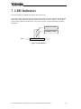
7. LED Indicators
This section applies to ASD-MULTICOM-A option boards only.
The interface board contains two bi-color red/green status LEDs. The lower LED indicates the Module
Status (MS), and the upper LED indicates the Network Status (NS). Refer to Figure 2. The use and
context of these LEDs is network-specific: refer to each network’s section in this manual for further
information.
NS (Network Status)
MS (Module Status)
PCB
Figure 2: LED Indicators
G7 ASD Multi-Protocol Communication Option and PG Feedback Option Manual
14
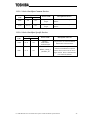
8. Network Configuration Parameters
This section applies to ASD-MULTICOM-A option boards only.
Because the Multicom interface supports several different fieldbus physical layers and protocols, some
configuration must be performed prior to inclusion on the network to inform the Multicom interface
which network it is being asked to communication via, and what the characteristics of that network are.
This configuration is performed by setting ASD parameters F890 ~ F894, which are collectively known
as the “Network Configuration Parameters”.
Note that the values of these 5 Network Configuration Parameters are only read by the Multicom
interface upon initialization after a drive reset or power-up condition. Therefore, if any of these
parameters are changed, be sure to reset the drive to enable the changes (as will be explained later, this
may actually involve resetting the drive twice: once when changing the “Network Selection” parameter
to validate the chosen network, and then once more when changing any of the configuration items
associated with the chosen network). Also note that although parameters F890 ~ F894 are always
available, whether or not all of these configuration parameters are actually used by the Multicom
interface will depend on the Multicom interface’s firmware version and the selected network.
The primary network selection is chosen by parameter F890 (refer to Table 4).
Table 4: Network Selection
Parameter
Function
F890
Network
Selection
Settings
0: Profibus DP
1: Modbus RTU
2: DeviceNet
Default Value
0
The function and adjustment ranges assigned to parameter F890 are fixed; that is to say that parameter
F890 is always the “Network Selection” parameter. The functions and adjustment ranges of the
remaining network configuration parameters (F891 ~ F894), however, will vary based on the setting of
parameter F890. For example, when parameter F890 is configured for Profibus DP communications,
then parameter F891 is unused, and its upper and lower adjustment limits will both be “0”. When
parameter F890 is configured for Modbus RTU communications, however, then parameter F891 is used
to select the Modbus network baud rate, and its adjustment range then becomes 0 ~ 7.
As previously mentioned, the values of the Network Configuration Parameters are validated by the
Multicom interface only during a drive initialization procedure. Therefore, when the drive and the
Multicom interface are initializing, the settings of the Network Configuration Parameters are read and
internally saved by the Multicom interface. These internally-saved values will not change until the next
initialization procedure. For this reason, two drive resets may be required when modifying the Network
Configuration Parameters: one to change and validate the network selection (parameter F890), and
another one to change and validate the remaining Network Configuration Parameters (parameters F891
~ F894) if necessary.
This behavior may best be explained through the use of an example. Say, for instance, that the
Multicom interface is currently configured for Profibus DP communications (parameter F890 = 0).
Let’s also say that we would like to reconfigure the Multicom interface to communicate via Modbus
RTU at 38.4kbaud with even parity, and that all configuration parameters are currently at their factorydefault values:
1.
Apply power to the drive. The drive and Multicom interface initialize. Parameter F890 is set
to 0, so the Multicom interface internally configures itself for Profibus DP communications.
G7 ASD Multi-Protocol Communication Option and PG Feedback Option Manual
15
2.
Change parameter F890 from its current setting of “0” to “1” to select Modbus RTU
communications. Press the “ENTER” key on the drive’s panel to write the change. At this
point, the Multicom interface is still configured for Profibus DP communications, so
parameters F891 ~ F894 will not be adjustable beyond “0”.
3.
Reset the drive (fault the drive and reset it, or momentarily power it off). Now, parameter
F890 is set to 1 during initialization, so the Multicom interface internally configures itself for
Modbus RTU communications.
4.
Now when we inspect parameter F891 (now “Modbus baud rate”), the value will be 5.
Therefore, we need to change parameter F891 from its current setting of “5” (9600 baud) to
“7” (38.4kbaud). Press the “ENTER” key on the drive’s panel to write the change. At this
point, the internal Modbus baud rate is still configured for 9600 baud (until the next
initialization sequence takes place).
5.
Similarly, change parameter F892 (now “Modbus parity & stop bits”) from its factory-default
value of “1” (no parity/2 stop bits) to “2” (even parity).
6.
Reset the drive once more. Now, when the drive and Multicom interface initialize, the
Multicom interface will initialize with Modbus RTU communications at 38.4kbaud and even
parity. The network configuration is now completed.
Once the network configuration parameters are configured for a specific network, their settings for that
network will be retained even if a different network is chosen and the second network’s configuration
parameters changed. Continuing with the above example for demonstration, even if a different network
is chosen, and parameters F891 ~ F894 associated with that network are changed, and then Modbus
RTU communications are once again selected by changing parameter F890 to “1”, the Modbus baud
rate will still be set to 38.4kbaud, and the parity will still be set to “even” when drive/Multicom
initialization has completed.
8.1 Profibus DP Configuration
When parameter F890 is selected for Profibus DP communications, no additional network configuration
is required. The additional Network Configuration Parameters, therefore, are unused (refer to Table 5).
Table 5: Profibus DP Network Configuration Parameters
Parameter
Function
Settings
Default Value
F891
Unused
N/A (Always 0)
0
F892
Unused
N/A (Always 0)
0
F893
Unused
N/A (Always 0)
0
F894
Unused
N/A (Always 0)
0
G7 ASD Multi-Protocol Communication Option and PG Feedback Option Manual
16
8.2 Modbus RTU Configuration
When parameter F890 is selected for Modbus RTU communications, then the additional Network
Configuration Parameters are assigned the functions as indicated in Table 6.
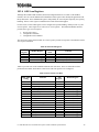
Table 6: Modbus RTU Network Configuration Parameters
Parameter
Function
Settings
0: 300 baud
1: 600 baud
2: 1200 baud
3: 2400 baud
4: 4800 baud
5: 9600 baud
6: 19.2 kbaud
7: 38.4 kbaud
0: no parity (1 stop bit)
1: no parity (2 stop bits)
2: even parity
3: odd parity
Default Value
F891
Baud Rate
F892
Parity & Stop Bits
F893
Response Delay
0 ~ 200 (0.00s ~ 2.00s)
0
F894
Unused
N/A (Always 0)
0
G7 ASD Multi-Protocol Communication Option and PG Feedback Option Manual
5
1
17
8.3 DeviceNet Configuration
When parameter F890 is selected for DeviceNet communications, then the additional Network
Configuration Parameters are assigned the functions as indicated in Table 7.
Table 7: DeviceNet Network Configuration Parameters
Parameter
Function
F891
Baud Rate
F892
Network
Communication
Loss Action
F893
Selected I/O
Assembly
Instance Set
F894
Unused
Settings
0: 125kbaud
1: 250kbaud
2: 500kbaud
0 = Set all consumed data to 0
1 = Retain last data values
2 = Issue STOP command to drive
3 = Issue EMERGENCY OFF
command to drive
4 = Run preset speed #1
5 = Run preset speed #2
6 = Run preset speed #3
7 = Run preset speed #4
8 = Run preset speed #5
9 = Run preset speed #6
10 = Run preset speed #7
11 = Run preset speed #8
12 = Run preset speed #9
13 = Run preset speed #10
14 = Run preset speed #11
15 = Run preset speed #12
16 = Run preset speed #13
17 = Run preset speed #14
18 = Run preset speed #15
0: Toshiba-specific
1: Basic speed control
2: Extended speed control
N/A (Always 0)
G7 ASD Multi-Protocol Communication Option and PG Feedback Option Manual
Default Value
0
0
0
0
18
9. Profibus Interface
This section applies to ASD-MULTICOM-A option boards only.
9.1 Feature Summary
The Multicom interface provides a wide array of network data access and drive control features.
Combined with the flexible configuration and high-speed data transfer capabilities of the Profibus
network, this allows powerful networked control and monitoring systems to be designed. Some of the
main features provided by the Multicom interface which allow for this control and configurability are
briefly described here:
Protocol
Profibus DP (Decentralized Periphery) as specified in European standard EN 50170. The Multicom
interface can also co-exist simultaneously on networks using Profibus-FMS.
Network Baud Rates
Supports all Profibus baud rates from 9.6kbaud to 12Mbaud. The network baud rate is automatically
detected and continuously monitored during operation; no parameter settings are necessary.
Power Supply
Self-contained. Powered directly from the connected drive. No external power supply devices or
connections are required.
Isolation
The drive is fully optically isolated from the Profibus network. By using optically isolated connections,
grounding differential problems are eliminated and noise immunity characteristics are greatly improved.
Global Control Functions
• Freeze mode:
Input (monitor) data values are held constant within the Multicom interface until
the next “freeze” command or an “unfreeze” command is received. Used
primarily for synchronized monitoring of multiple Profibus nodes.
• Sync mode:
Output (control) data values are held constant within the Multicom interface until
the next “sync” command or an “unsync” command is received. Used primarily
for synchronized control of multiple Profibus nodes.
• Clear_Data:
All output (control) data values are cleared to “0”.
Network Watchdog
A network watchdog function is always operating within the Multicom interface (if selected at time of
unit commissioning). In the event of a disconnection from the Profibus network or loss of the network
master, the Multicom interface will automatically set its control data to 0.
G7 ASD Multi-Protocol Communication Option and PG Feedback Option Manual
19
Indicator
A green LED (LED1) is provided to indicate when the Multicom interface has achieved the
DATA_EXCHANGE state with the Profibus network master. This serves as a convenient indicator that
the Profibus master and Multicom interface are configured properly and are exchanging data.
Profibus Network Connector
The network interface is a standard DB-9 female connector. The metallic housing of the DB-9
connector is typically connected to the network shield in the attached Profibus connector. The DB-9
housing can, in turn, then be connected to earth ground if desired.
Input/Output Data
The Multicom interface’s cyclic output (control) and input (status) data sizes are selectable (modular) in
16 different configurations representing sizes of between 4 and 40 bytes.
Via these data structures, any data item (command data, monitor data and configuration parameters)
available in the drive can be accessed. For detailed explanations of the format and usage of the
input/output data, refer to section 9.4.
G7 ASD Multi-Protocol Communication Option and PG Feedback Option Manual
20
9.2 Profibus Interface Connection
Table 8 provides DB-9 connector pin descriptions for Profibus connector CN3.
Table 8: Pin description for Profibus connector CN3
Pin
Number
1
2
3
4
5
6
7
8
9
Function
No connection
No connection
Profibus network “B” (positive) data line
RTS signal – direction control for fiber optic network interface
DGND – power supply ground internally connected to the interface
board’s isolated ground
VP – power supply +5v internally connected to the interface board’s
isolated P5.
No connection
Profibus network “A” (negative) data line
RTS signal ground reference – internally connected to the interface
board’s isolated ground
In/Out
In/out
Out
In/out
-
To connect to the Multicom interface, complete the following steps:
1.
Connect the Profibus network cable to the DB9 connector marked “CN3” on the G7 Multicom
Option. Refer to the Profibus Specification for detailed network wiring guidelines. Ensure that the
Profibus network cable is tightly screwed onto the DB9 connector, and route the cable such that it is
located well away from any drive input power or motor wiring. Also take care to route the cable
away from any sharp edges or positions where it may be pinched.
2.
Grounding is of particular importance for reliable, stable operation. Communication system
characteristics may vary from system to system, depending on the system environment and
grounding method used. The metallic housing of the DB9 connector (CN3) will be regarded as the
“Shield GND” of the Multicom interface. The “Shield GND” should be connected to the shield of
the Profibus network cable through the Profibus connector. To ground the network cable shield,
therefore, connect a wire to the “Shield GND”, and then connect the other end of the wire to an
appropriate ground. For specific requirements regarding protective grounding and the Profibus
network, refer to the Profibus Standard (EN 50 170, part 1).
9.3 Unit Addressing
The Profibus node (slave) address is set via parameter F802 (inverter number parameter). Although
parameter F802 has an adjustment range from 0-255, only 0-126 is an allowable addressing selection for
the Profibus network. Therefore, if parameter F802 is set to 127 through 255, the Multicom interface
will default to an address of 126.
G7 ASD Multi-Protocol Communication Option and PG Feedback Option Manual
21
9.4 Profibus Exchanged Data Structures
9.4.1 Output (Control) Data Format
The size of the output data structure from the network master to the Multicom interface is modular and
selectable from 4 to 40 bytes. The allocation of the maximum 40 bytes of the data structure is
comprised of 1 fixed four-byte command, 1 fixed four-byte extended command, 1 fixed four-byte speed
reference, 5 configurable four-byte scan data selections (selectable via drive parameters F831-F835),
and 1 eight-byte structure for asynchronous parameter accesses. Refer to Table 9 for details.
Table 9: Output (Control) data
Offset
Data
Offset
Data
0
1
2
3
4
5
6
7
8
9
10
11
12
13
14
15
16
17
18
19
Reserved
Reserved
Command high byte
Command low byte
Reserved
Reserved
Extended command high byte
Extended command low byte
Speed reference high byte
:
:
Speed reference low byte
Parameter F831 setting high byte
:
:
Parameter F831 setting low byte
Parameter F832 setting high byte
:
:
Parameter F832 setting low byte
20
21
22
23
24
25
26
27
28
29
30
31
32
33
34
35
36
37
38
39
Parameter F833 setting high byte
:
:
Parameter F833 setting low byte
Parameter F834 setting high byte
:
:
Parameter F834 setting low byte
Parameter F835 setting high byte
:
:
Parameter F835 setting low byte
Action bits / Reserved
Reserved
Parameter number high byte
Parameter number low byte
Reserved
Reserved
Parameter data to write high byte
Parameter data to write low byte
Locations marked “Reserved” in the above table are reserved for future use. Presently, all “Reserved”
output data locations are ignored by the drive. Future releases of the drive firmware, however, may use
these locations for data transfer.
Throughout the remainder of this section, references may be made to internal ASD parameter numbers
and data definitions. For more information regarding the specific accessible ASD parameters, please
refer to the appropriate ASD Serial Communication Interface Manual (obtainable from Toshiba).
G7 ASD Multi-Protocol Communication Option and PG Feedback Option Manual
22
•
Command Word (Offsets 2 and 3)
Bit-mapped drive command word internally located at parameter 0xFA06. Table 10 provides the format
of this command word.
Table 10: Command Word Format
Function
0
1
15
14
13
12
11
10
9
8
7
6
5
4
3
2
1
0
Command priority
Speed reference priority
Control selection
Emergency OFF command
Coast stop command
Error counter reset command
Forward / reverse selection
Jog command
DC injection braking command
PI control OFF command
Brake release command
Excitation current command
Brake close command
Fault reset command
Reserved
Run / stop selection
N/A
N/A
Speed control
N/A
N/A
N/A
Forward
N/A
N/A
N/A
N/A
N/A
N/A
N/A
-Stop
Option priority
Option priority
Torque / position control
Emergency OFF
Coast stop
Reset
Reverse
Jog
DC injection braking
PI control OFF
Brake release
Excitation current
Brake close
Reset
-Run
Low Byte
High Byte
Bit
•
Extended Command Word (Offsets 6 and 7)
Bit-mapped drive extended command word internally located at parameter 0xFA23. Table 11 provides
the format of this extended command word.
Low Byte
High Byte
Table 11: Extended Command Word Format
Bit
Function
0
1
15
14
13
12
11
10
9
8
7
6
5
4
3
2
1
0
Reverse jog command
Forward jog command
Torque limit selection bit 2
Torque limit selection bit 1
V/F selection bit 2
V/F selection bit 1
Accel/decel selection bit 2
Accel/decel selection bit 1
Brake test command
Brake response command
Reserved
Reserved
Preset speed selection bit 4
Preset speed selection bit 3
Preset speed selection bit 2
Preset speed selection bit 1
N/A
N/A
2: Torque limit 3
0: Torque limit 1
2: V/F 3
0: V/F 1
2: Accel/decel 3
0: Accel/decel 1
Brake close
Brake close
--12: 12th speed 13: 13th speed
8: 8th speed
9: 9th speed
th
4: 4 speed
5: 5th speed
0: OFF
1: 1st speed
Jog reverse
Jog forward
3: Torque limit 4
1: Torque limit 2
3: V/F 4
1: V/F 2
3: Accel/decel 4
1: Accel/decel 2
Brake release
Brake release
--14: 14th speed 15: 15th speed
10: 10th speed 11: 11th speed
6: 6th speed
7: 7th speed
nd
2: 2 speed
3: 3rd speed
G7 ASD Multi-Protocol Communication Option and PG Feedback Option Manual
23
•
Speed Reference Command (Offsets 8 ∼ 11)
Unsigned 16-bit value located at parameter 0xFA07. The data contained in the speed reference
command word is the desired speed reference command multiplied by 100, and then converted to
hexadecimal. In other words, if a speed reference command of 55.34Hz is desired, then 55.34 x 100 =
5534, which converted to hexadecimal is 0x159E. The speed reference command low byte (offset 11)
must therefore contain 0x9E and the next-highest byte (offset 10) must contain 0x15.
If the speed reference command exceeds limiting drive parameters (such as the Upper Limit Frequency
or Maximum Frequency), then the drive will ignore it, maintaining its current setting.
•
Drive Command Scan Data (Offsets 12 ∼ 31)
Table 12 provides a list of the available command scan data selections (selectable via drive parameters
F831∼F835). The “Parameter” column indicates the drive’s internal parameter to which the
corresponding selection is mapped.
Table 12: Drive Command Scan Data
F831∼
∼F835
Setting
Description
Unit
Range
Parameter
0
1
2
3
4
5
6
7
8
9
10
11
12
13
14
15
16
No selection
RESERVED
RESERVED
Incremental speed reference
Absolute torque limit
Positive torque limit
Negative torque limit
Torque command
Speed torque bias
Tension torque bias
Load balance gain
Drooping gain
Speed loop proportional gain
Speed loop integral gain
Output terminals
Load moment of inertia
RESERVED
0.01Hz
0.01%
0.01%
0.01%
0.01%
0.01%
0.01%
0.01
0.01
0.1
0.1
0.0001
-
0 ~ 500
0 ~ 25000
0 ~ 25000
0 ~ 25000
-25000 ~ 25000
-25000 ~ 25000
-25000 ~ 25000
0 ~25000
0 ~ 10000
32 ~ 10000
100 ~ 2000
100 ~ 10000
-
0xFFFF
0xFA08
0xFA34
0x0441
0x0443
0xFA33
0x0726
0x0727
0x0728
0x0320
0x0376
0x0377
0xFA50
0xFA35
-
Note 1: Items marked as “RESERVED” in Table 12 are reserved for future use. Selecting
one of the corresponding values as command scan data will have no effect on drive
operation.
Note 2: Although not disallowed, avoid configuring more than 1 scan command data
parameter with the same command data selection (for example, do not set both F831 and
F832 to “3”, etc.). Unexpected drive behavior could result if different data values are
written to the corresponding command locations.
Note 3: Parameters F831∼F835 are only validated on drive reset or power-up.
Therefore, if any of these parameters are changed, be sure to reset the drive to validate
the changes.
Note 4: Data range checking is not performed on command scan items. If a value outside
of a specific item’s valid range is written to the drive, that value will be accepted, but
ignored by the drive.
G7 ASD Multi-Protocol Communication Option and PG Feedback Option Manual
24
•
Action Bits / Parameter Number (Offsets 32 ∼ 35)
Parameter action bits and 16-bit parameter number. Refer to section 9.6 for a detailed explanation of
these items.
•
Parameter Data (Offsets 38 and 39)
During parameter writes, this contains the data to write. Refer to section 9.6 for a detailed explanation
of this location.
9.4.2 Input (Status) Data Format
The size of the input data structure from the Multicom interface to the network master is modular and
selectable from 4 to 40 bytes. The allocation of the maximum 40 bytes of the data structure is
comprised of 1 fixed four-byte status, 1 fixed four-byte output speed reference, 6 configurable four-byte
scan data selections (selectable via drive parameters F841-F846), and 1 eight-byte structure for
asynchronous parameter accesses. Refer to Table 13 for details.
Table 13: Input (Status) data
Offset
0
1
2
3
4
5
6
7
8
9
10
11
12
13
14
15
16
17
18
19
Data
Reserved
Reserved
Status high byte
Status low byte
Operating speed high byte
:
:
Operating speed low byte
Parameter F841 setting high byte
:
:
Parameter F841 setting low byte
Parameter F842 setting high byte
:
:
Parameter F842 setting low byte
Parameter F843 setting high byte
:
:
Parameter F843 setting low byte
Offset
Data
20
21
22
23
24
25
26
27
28
29
30
31
32
33
34
35
36
37
38
39
Parameter F844 setting high byte
:
:
Parameter F844 setting low byte
Parameter F845 setting high byte
:
:
Parameter F845 setting low byte
Parameter F846 setting high byte
:
:
Parameter F846 setting low byte
Response bits / Reserved
Reserved
Parameter number response high byte
Parameter number response low byte
Reserved
Reserved
Parameter data response high byte
Parameter data response low byte
Locations marked “Reserved” in the above table are reserved for future use. Presently, all “Reserved”
input data is set to 0 by the drive. Future releases of the drive firmware, however, may use these
locations for data transfer.
G7 ASD Multi-Protocol Communication Option and PG Feedback Option Manual
25
•
Status Word (Offsets 2 and 3)
Bit-mapped status word. Table 14 provides the format of this status word.
Low Byte
High Byte
Table 14 : Status Word Format
•
Bit
Function
0
1
15
Ready for operation status
(not including MOFF)
Drive healthy signal
Ready for operation status (not
including ST)
Ready for operation status
(including ST)
Control mode status
Speed limit status
Forward / reverse status
Jog status
DC injection braking
OL alarm status
PI control status
Alarm status
Serious fault status
Run / stop status
Alarm stop status
Fault status
Not ready
Ready
14
13
12
11
10
9
8
7
6
5
4
3
2
1
0
Alternating heartbeat: “0” for 1s, then “1” for 1s
Not ready
Ready
Not ready
Ready
Speed control
Normal
Forward
Normal
Normal
Normal
Normal
No alarm
Normal
Stopped
None
None
Torque / position control
Speed limiting
Reverse
Jogging
DC injection braking active
OL alarm
PI control inactive
Alarm
Serious fault
Running
Alarm stopped
Faulted
Operating Speed (Offsets 4 ∼ 7)
Obtained from drive parameter 0xFE58. Continuously reports the drive’s operating speed. In order to
determine the drive’s actual output speed, the data contained in the output speed must first be converted
from hexadecimal to decimal, and then divided by 100. For example, if offset #6 is 0x12 and offset #7
is 0x34, then 0x1234 converted to decimal is 4660. Dividing this number by 100, the actual operating
speed of 46.60Hz is obtained.
G7 ASD Multi-Protocol Communication Option and PG Feedback Option Manual
26
•
Drive Status Scan Data (Offsets 12 ∼ 31)
Table 15 provides a list of the available status scan data selections (selectable via drive parameters
F841-F846). The “Parameter” column indicates the drive’s internal parameter to which the
corresponding selection is mapped. More detailed explanations of some of these status items follow
Table 15.
Table 15: Drive Status Scan Data
F841~F846
Setting
0
1
2
3
4
5
6
7
8
9
10
11
12
13
14
15
16
Description
Unit
Range
Parameter
No selection
Alarm code monitor
Operating speed
Real-time speed feedback
Filtered speed feedback
Internal torque reference
Output current
Excitation current
Torque current
Overload value
Accel / Decel torque
reduction
Motor counter data
Fault code
Input terminal
VI input
RR input
RX input
0.01Hz
0.01Hz
0.01Hz
0.01%
0.01%
0.01%
0.01%
0.01%
0 ~ 40000
0 ~ 40000
0 ~ 40000
-32767 ~ 32767
0 ~ 32767
-32767 ~ 32767
-32767 ~ 32767
0 ~ 10000
0xFFFF
0xFC91
0xFE58
0xFE61
0xFE62
0xFE56
0xFE03
0xFE21
0xFE20
0xFE59
0.01%
-32767 ~ 32767
0xFE60
0.01%
0.01%
0.01%
0 ~ 65535
0 ~ 10000
0 ~ 10000
-10000 ~ 10000
0xFE33
0xFC90
0xFE06
0xFE36
0xFE35
0xFE37
Note 1: Parameters F841∼F846 are only validated on drive reset or power-up.
Therefore, if any of these parameters are changed, be sure to reset the drive to validate
the changes.
G7 ASD Multi-Protocol Communication Option and PG Feedback Option Manual
27
Alarm Code Monitor
Bit-mapped alarm code monitor word internally located at parameter 0xFC91. Table 16 provides the
format of this alarm code monitor word.
Table 16: Alarm Code Monitor Word Format
Function
0
1
15
14
13
12
Reserved
Reserved
Reserved
Communication error alarm
(logic / RS-485 / message transmission)
Communication error alarm
(scan transmission)
Cumulative run timer alarm
Dynamic braking resistor overload alarm
Over-torque alarm
Low current alarm
Low control power alarm
Low main power alarm
Over-voltage alarm
Overheat alarm
Motor overload alarm
Drive overload alarm
Over-current alarm
---N/A
---Alarm on
N/A
Alarm on
N/A
N/A
N/A
N/A
N/A
N/A
N/A
N/A
N/A
N/A
N/A
Alarm on
Alarm on
Alarm on
Alarm on
Alarm on
Alarm on
Alarm on
Alarm on
Alarm on
Alarm on
Alarm on
Low Byte
High Byte
Bit
11
10
9
8
7
6
5
4
3
2
1
0
Fault Code
Current fault code internally located at parameter 0xFC90. Table 17 provides the list of fault codes with
descriptions.
Table 17: Fault Codes
Fault Code
0000
0001
0002
0003
0004
0005
0006
0007
0008
0009
000A
000B
000C
000D
000E
000F
0010
0011
Fault Description
No error
Over-current fault during acceleration
Over-current fault during deceleration
Over-current fault during constant-speed run
Load-side over-current fault at start-up
Over-current fault of U-phase arm
Over-current fault of V-phase arm
Over-current fault of W-phase arm
Input error-phase fault
Output error-phase fault
Over-voltage fault during acceleration
Over-voltage fault during deceleration
Over-voltage fault during constant running speed
Drive overload
Motor overload
Dynamic braking resistor overload
Overheat
Emergency OFF
G7 ASD Multi-Protocol Communication Option and PG Feedback Option Manual
Panel Display
NERR
OC1
OC2
OC3
OCL
OCA1
OCA2
OCA3
EPH1
EPHO
OP1
OP2
OP3
OL1
OL2
OLR
OH
E
28
Fault Code
0012
0013
0014
0015
0016
0017
0018
0019
001A
001B
001C
001D
001E
001F
0020
0021
0022
0023
0024
0025
0026
0027
0028
0029
002A
002B
002C
002D
002E
0031
Fault Description
EEPROM write error
EEPROM initial read error (control EEPROM)
EEPROM initial read error (main circuit EEPROM)
Main RAM error
Main ROM error
CPU error
Communication interruption error
Gate array error
Output current detect fault
Option board error
Flash memory error
Under-current fault
Under-voltage fault (main power)
Under-voltage fault (control power)
Over-torque fault
Earth fault (software detection)
Earth fault (hardware detection)
Fuse error
Dynamic braking resistor over-current fault
DC section over-current fault during acceleration
DC section over-current fault during deceleration
DC section over-current fault during constant-speed run
Automatic tuning error
Drive type error
Sink / source selection error
Electromagnetic brake error
Encoder disconnected fault
Speed error
Positioning error
Key error
G7 ASD Multi-Protocol Communication Option and PG Feedback Option Manual
Panel Display
EEP1
EEP2
EEP3
ERR2
ERR3
ERR4
ERR5
ERR6
ERR7
ERR8
ERR9
UC
UP1
UP2
OT
EF1
EF2
EFU
OCR
OC1P
OC2P
OC3P
ETN
ETYP
E-10
E-11
E-12
E-13
E-14
E-17
29
Input Terminals
Bit-mapped input terminal word internally located at parameter 0xFE06. Table 18 provides the format
of this input terminal word.
Low Byte
High Byte
Table 18: Input Terminals
•
Bit
Terminal Name
(Expansion Terminals)
Function
Parameter
Number
0
1
15
14
13
12
11
10
9
8
7
6
5
4
3
2
1
0
(B15)
(B14)
(B13)
(B12)
(B11)
(B10)
(B9)
(B8)
S4
S3
S2
S1
RES
ST
R
F
Input terminal selection 16
Input terminal selection 15
Input terminal selection 14
Input terminal selection 13
Input terminal selection 12
Input terminal selection 11
Input terminal selection 10
Input terminal selection 9
Input terminal selection 8
Input terminal selection 7
Input terminal selection 6
Input terminal selection 5
Input terminal selection 4
Input terminal selection 3
Input terminal selection 2
Input terminal selection 1
F126
F125
F124
F123
F122
F121
F120
F119
F118
F117
F116
F115
F114
F113
F112
F111
OFF
OFF
OFF
OFF
OFF
OFF
OFF
OFF
OFF
OFF
OFF
OFF
OFF
OFF
OFF
OFF
ON
ON
ON
ON
ON
ON
ON
ON
ON
ON
ON
ON
ON
ON
ON
ON
Response Bits / Parameter Number (Offsets 32 ∼ 35)
Parameter response bits and 16-bit parameter number. Refer to section 9.6 for a detailed explanation of
these items.
•
Parameter Data (Offsets 38 and 39)
During parameter reads, this word contains the requested data response. Refer to section 9.6 for a
detailed explanation of this location.
G7 ASD Multi-Protocol Communication Option and PG Feedback Option Manual
30
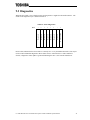
9.5 Diagnostics
When the drive faults, 1 byte of high-priority user diagnostics is supplied to the Profibus master. The
format of the diagnostics byte is shown in Table 19.
7
6
5
4
3
2
1
0
Reserved
Reserved
Reserved
Reserved
Reserved
Reserved
Drive Faulted
Bit #:
Reserved
Table 19: Drive Diagnostics
Reserved bits indicated in the above table are currently set to “0” by the Multicom interface, but may be
used to transfer additional diagnostics data in future releases. When the drive’s fault condition is
cleared, a diagnostics status update is generated indicating the drive’s exit from the faulted state.
G7 ASD Multi-Protocol Communication Option and PG Feedback Option Manual
31
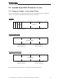
9.6 Asynchronous Drive Parameter Access
9.6.1 Parameter Number / Action Output Words
To access drive parameters, 2 output words and 2 action bits are provided in the drive’s output data
structure. The structure of these output words and action bits is as follows:
15
14
13
12
Reserved
Req1
Req0
Bit #:
Reserved
Action Bits
11
8
7
4
3
0
Reserved
Action bits (offset 32)
Reserved (offset 33)
Parameter Number Word
Bit #:
15
12
11
8
7
4
3
0
Parameter number
Parameter number
high byte (offset 34)
Parameter number
low byte (offset 35)
Parameter Data Write Word
Bit #:
15
12
11
8
7
4
3
0
Parameter data
Parameter data to write
high byte (offset 38)
Parameter data to write
low byte (offset 39)
Note that all locations marked “Reserved” are ignored by the Multicom interface.
G7 ASD Multi-Protocol Communication Option and PG Feedback Option Manual
32
9.6.2 Parameter Number / Action Input Words
The response by the Multicom interface to parameter read and write requests is placed in 2 input words
and 2 input bits of the input data structure. The structure of these data items is as follows:
15
14
13
12
Reserved
Resp1
Resp0
Bit #:
Reserved
Response Bits
11
8
7
4
3
0
Reserved
Action response bits
(offset 32)
Reserved (offset 33)
Parameter Number Response Word
Bit #:
15
12
11
8
7
4
3
0
Parameter number
Parameter number response high byte
(offset 34)
Parameter number response low byte
(offset 35)
Parameter Data / Error Code Response Word
Bit #:
15
12
11
8
7
4
3
0
Parameter data / error code
Parameter data response
high byte (offset 38)
Parameter data response
low byte (offset 39)
Note that all locations marked “Reserved” are set to 0 by the Multicom interface.
G7 ASD Multi-Protocol Communication Option and PG Feedback Option Manual
33
9.6.3 Drive Parameter Access Procedure
In order to read from a drive parameter or write to a drive parameter, two control bits are provided in
the drive’s output data structure. These bits, labeled Req1 and Req0 in the Action Bits word, can have
the following values:
Req1
0
0
1
1
Req0
Meaning
0.............. No action (idle state)
1.............. Parameter read
0.............. Parameter write (RAM & EEPROM)
1.............. Parameter write (RAM only)
Similarly, when the drive responds to a parameter read or write request, two status bits are provided in
the drive’s input data structure. These bits, labeled Resp1 and Resp0 in the Action Bits Response word,
can have the following values:
Resp1
0
0
1
1
Resp0
Meaning
0.............. No action (idle state acknowledge)
1.............. Parameter read success acknowledge
0.............. Parameter write success acknowledge
1.............. Error indication
Note that the Multicom interface will respond with Resp1:Resp0 = 1:0 upon a successful parameter
write, regardless of whether the write was to RAM & EEPROM or to RAM only.
Performing a parameter read or write action from the Profibus master involves the following process:
1.
Send a “no action” code (Req1=0 and Req0=0). Every parameter access must begin from the
idle state. Once this state is sent, the Profibus master must then wait for the Multicom interface
to respond with an idle state acknowledge (Resp1=0 and Resp0=0).
2.
If the action is to be a data write, set the parameter data in the parameter data write word. If
the action is to be a data read, the parameter data write word value is irrelevant.
3.
Set the parameter number and action code (Req1 and Req0). For an explanation of parameter
numbers, refer to section 9.7.
4.
Once the Multicom interface receives the read or write request, it will begin processing it. The
time required to complete the request depends primarily on the specific register being
requested and the drive’s internal state at the time of the request, but can vary from several
milliseconds to several tens of milliseconds.
5.
Once the Multicom interface has completed the request, it will place its response in the action
bits response, parameter number response, and data / error code response locations:
•
If the request was a read, and the read was performed successfully, this will be indicated to the
master by Resp1:Resp0 changing from 0:0 to 0:1. The parameter number response will equal
the accessed parameter number, and the resulting data read will be placed in the data / error
code response word.
•
If the request was a write, and the write was performed successfully, this will be indicated to
the master by Resp1:Resp0 changing from 0:0 to 1:0. The parameter number response will
equal the accessed parameter number, and the data written to the drive will be reflected in the
data / error code response word.
•
If an error occurred during the read or write request, this will be indicated to the master by
Resp1:Resp0 changing from 0:0 to 1:1. The parameter number response will equal the
parameter number that the master was attempting to access, and an error code reflecting the
failure cause will be placed in the data / error code response word. For a list of possible error
codes, refer to section 9.6.4.
G7 ASD Multi-Protocol Communication Option and PG Feedback Option Manual
34
6.
In order to perform another parameter read or write, the master must once again send a “no
action” code (Req1=0 and Req0=0), and the Multicom interface must once again respond with
an idle state acknowledge (Resp1=0 and Resp0=0) before the next read or write action can take
place. Until a “no action” code is sent to the Multicom interface, the interface will ignore all
data in the action bits, parameter number and parameter write data words. Also, as long as the
master sends the “no action” code, the Multicom interface will loop-back in the parameter
number response word and parameter data / error code response word whatever data is sent to
it in the corresponding output words.
9.6.4 Register Access Error Codes
When a parameter read or write error occurs, one of the following error codes will be returned in the
parameter data response word:
Error Code
Meaning
0x0000 ..................... cannot execute (access error)
0x0001 ..................... data error (written data value outside of valid range)
0x0002 ..................... invalid parameter number
0x0064 ..................... attempt to write to a read-only parameter
0x0065 ..................... attempt to read from a write-only parameter
0x0066 ..................... other / unclassified error
9.7 Parameters
The parameters that can be accessed via the parameter access method outlined in section 9.6 are defined
in the Toshiba ASD Operation Manual and/or the ASD Serial Interface Manual. The accessible
parameters, their access behaviors and data ranges may vary depending on the drive’s firmware revision.
The following parameters, which are not implemented in the drive, are used to access local information
on the Multicom interface:
Parameter
Function
Read / Write
Adjustment Range
0xFC82
Multicom interface firmware
version/revision
Read only
High byte = firmware version
Low byte = firmware revision
If an attempt is made to write to this register, error code number 0x0064 (WRITE_TO_READONLY)
will be returned in the parameter data/error code field of the acyclic data.
G7 ASD Multi-Protocol Communication Option and PG Feedback Option Manual
35
10. RS-485 Interface
This section applies to ASD-MULTICOM-A option boards only.
10.1 Physical Layer
Figure 3 shows the physical layer for the RS-485 portion of the Multicom interface. This circuit
diagram is provided as an aid to the system (network) designer to ensure that externally-connected
circuitry will provide the required voltages etc. necessary for sufficient and robust communications.
P5ISO
R37
47k
TB1:9
A
B
ZD1
6.2V
ZD3
6.2V
ZD2
6.2V
ZD4
6.2V
GNDISO
GNDISO
TB1:10
RS-485
NETWORK
R38
47k
GNDISO
TB1:11
R26
200
GNDISO
Figure 3: RS-485 Physical Layer
G7 ASD Multi-Protocol Communication Option and PG Feedback Option Manual
36
10.2 Modbus RTU
10.2.1 Configuration
Besides the Modbus network selection and configuration parameters (F890-F894) described in Section
8.2, the only other ASD parameter requiring configuration is the ASD’s “Inverter Number” parameter
(F802). This parameter setting is used as the drive’s Modbus station address.
Some important points to note regarding parameter F802:
•
Parameter F802 is only validated after a drive reset. Therefore, if this parameter is changed,
remember to reset the drive to validate the change.
•
The standard factory setting for parameter F802 is 0, which is reserved for Modbus broadcast
transmissions. To be valid, this parameter must be set to a value between 1 and 247. If parameter
F802 is 0 or 248 ∼ 255 when Modbus communications are initialized, the Multicom interface’s
“Network Status” LED (the lower LED) will flash red to indicate the configuration error, and
network communications will not be enabled.
If ASD control (frequency command input, RUN/STOP, etc.) is to be performed via the Modbus
network, then the drive’s Command Mode Selection and/or Frequency Mode Selection parameters must
be configured to use the communication card as the drive’s command source location, or the “option
priority” bits of the basic command word (Modbus register 0x0A07) must be set accordingly. For
information on the specific setting methods and values of the Command Mode and Frequency Mode
Selection parameters, please refer to the G7 Adjustable Speed Drive Operation Manual.
10.2.2 Communication Formats
A brief note about Modbus communication formats: According to the Modicon Modbus Protocol
Reference Guide, the specifications for the Modbus RTU communication mode is as follows:
Coding System: ............... 8-bit binary, hexadecimal 0 ∼ 9, A ∼ F
Two hexadecimal characters contained in each 8-bit field of the message
Bits per Byte: .................. 1 start bit
8 data bits, least significant bit sent first
1 bit for even/odd parity; no bit for no parity
1 stop bit if parity is used; 2 bits if no parity
Error Check Field: ......... Cyclical Redundancy Check (CRC)
According to the Modicon Modbus specification, therefore, the number of bits per byte in RTU mode is
1 start + 8 data + 1 parity + 1 stop (if parity is used), or 1 start + 8 data + 2 stop (if parity is not used),
resulting in an RTU data frame that is fixed at 11 bits per byte.
In addition to these standard specified data frame sizes, the Multicom Modbus interface offers an
optional configuration of providing for only 1 stop bit when no parity is selected. As indicated in Table
6 on page 17, by setting parameter F892 (Parity & Stop Bits) to “0”, the RTU data frame size is
modified to consist of 1 start + 8 data + 1 stop bit = 10 bits per byte.
G7 ASD Multi-Protocol Communication Option and PG Feedback Option Manual
37
10.2.3 Modbus/ASD Register Mappings
The Multicom Modbus interface acts as a relatively straightforward network gateway for the ASD into
which it is installed. In general, Modbus holding registers (4X references) are directly mapped to
corresponding ASD registers (also sometimes referred to as “communication numbers” or “parameter
numbers”) with a direct 1-to-1 correspondence. The relationship between Modbus holding registers and
their ASD register counterparts is as follows:
Modbus holding register = ASD register + 1
This means that in order to access a specific ASD register, simply add 1 to its index and access that
Modbus holding register. The reason for this offset is due to the fact that ASD registers begin at index
0, while Modbus holding registers begin at index 1.
The only minor exception to the above 1-to-1 mapping takes place in the “upper address” registers in the
ASD. By inspecting the Toshiba Serial Communications Manual, one can observe that the ASD
registers are divided into two distinct regions within the full 0x0000 ~ 0xFFFF ASD register map: the
“lower address” range covers from 0x0000 to 0x09FF, and the “upper address” range covers from
0xFA00 to 0xFFFF (not all values within those ranges access valid ASD registers, of course). For
access consistency and because some Modbus clients are unable to access holding registers with indexes
greater than 999910 (0x270F), the Multicom Modbus interface automatically maps all “upper address”
ASD registers into the contiguous region immediately following the “lower address” range. To take
advantage of this feature, simply drop the initial “F” on any register index in the “upper address” range
(and add 1 to that number to obtain the corresponding Modbus register), and the register request will
automatically access the correct internal ASD register.
For example, if we wish to read ASD register 0xFE06 (input terminal status), we would change the
0xFE06 to 0x0E06, and then add 1 to obtain the resultant Modbus register: 0x0E07 (359110).
Therefore, making a request to read Modbus register 0x0E07 will return the input terminal status located
at ASD register 0xFE06. If desired, it is also acceptable to access the “upper address” registers at their
original locations, as their default (0xFXXX) locations can still be accessed. Continuing with the
previous example, ASD register 0xFE06 can therefore be equally accessed by requesting either Modbus
register 0x0E07 or 0xFE07 (6503110).
In order to avoid any possible confusion regarding this register-mapping scheme, this manual will
always explicitly use the terms “ASD register” or “Modbus register” where the intended usage may not
be clear. If the term “register” is used alone, then “Modbus register” will be the intended meaning by
default.
With the exception of the “upper address” register mapping feature explained above and the
programmable pointer registers feature detailed in Section 10.2.6, the Multicom Modbus interface does
not in any way modify or otherwise alter valid register access requests originating from the Modbus
client. By adhering to this design parameter, the availability and interpretation of any Modbus registers
is entirely determined by the attached drive. In this way, the Modbus interface allows itself to become
virtually “transparent” on the network, essentially allowing the Modbus client to carry on a dialog
directly with the drive.
An overview of the entire mapping configuration can be found in Section 10.2.9.
G7 ASD Multi-Protocol Communication Option and PG Feedback Option Manual
38
10.2.4 ASD Scan Registers
Although all available ASD command, status and configuration data is accessible via the Modbus
interface, there are certain fundamental command and status registers that virtually all applications will
likely find useful. These fundamental registers will probably be accessed quite frequently, and “priority
handling” of these select registers would therefore benefit network throughput.
For this reason, certain ASD registers can be configured for special handling, which provides very fast
access response. These registers are referred to as “scan registers”. The Multicom Modbus interface
provides three types of scan registers:
1.
2.
3.
Fixed (read or write)
Configurable read/status
Configurable write/command
The fixed scan registers listed in Table 20. These registers provide fast response to the indicated read or
write request at all times.
Table 20: Fixed Scan Registers
ASD
Register
0xFA06
0xFA23
0xFA07
0xFE58
Modbus Register
0x0A07 (256710)
0x0A24 (259610)
0x0A08 (256810)
0x0E59 (367310)
Read /
Write
Write
Write
Write
Read
Function
Basic command
Extended command
Option board frequency command
Output frequency
Table 21 provides a list of the available read/status scan selections. These are selectable via drive
parameters F841-F846, which allows a total of six read scan registers to be configured.
Table 21: Drive Status Scan Data
F841~F846
Setting
0
1
2
3
4
5
6
7
8
9
10
11
12
13
14
15
16
Function
No selection
Alarm code monitor
Output frequency
Real-time speed feedback
Filtered speed feedback
Internal torque reference
Output current
Excitation current
Torque current
Overload value
Accel / Decel torque reduction
Motor counter data
Fault code
Input terminal
VI input
RR input
RX input
ASD
Register
Modbus Register
N/A
0xFC91
0xFE58
0xFE61
0xFE62
0xFE56
0xFE03
0xFE21
0xFE20
0xFE59
0xFE60
0xFE33
0xFC90
0xFE06
0xFE36
0xFE35
0xFE37
N/A
0x0C92 (321810)
0x0E59 (367310)
0x0E62 (368210)
0x0E63 (368310)
0x0E57 (367110)
0x0E04 (358810)
0x0E22 (361810)
0x0E21 (361710)
0x0E5A (367410)
0x0E61 (368110)
0x0E34 (363610)
0x0C91 (321710)
0x0E07 (359110)
0x0E37 (363910)
0x0E36 (363810)
0x0E38 (364010)
G7 ASD Multi-Protocol Communication Option and PG Feedback Option Manual
39
Table 22 provides a list of the available write/command scan selections. These are selectable via drive
parameters F831-F835, which allows a total of five write scan registers to be configured.
Table 22: Drive Command Scan Data
F831∼
∼F835
Setting
0
1
2
3
4
5
6
7
8
9
10
11
12
13
14
15
16
Function
No selection
RESERVED
RESERVED
Incremental speed reference
Absolute torque limit
Positive torque limit
Negative torque limit
Torque command
Speed torque bias
Tension torque bias
Load balance gain
Drooping gain
Speed loop proportional gain
Speed loop integral gain
Output terminals
Load moment of inertia
RESERVED
ASD
Register
Modbus Register
N/A
N/A
N/A
0xFA08
0xFA34
0x0441
0x0443
0xFA33
0x0726
0x0727
0x0728
0x0320
0x0376
0x0377
0xFA50
0xFA35
N/A
N/A
N/A
N/A
0x0A09 (256910)
0x0A35 (261310)
0x0442 (109010)
0x0444 (109210)
0x0A34 (261210)
0x0727 (183110)
0x0728 (183210)
0x0729 (183310)
0x0321 (80110)
0x0377 (88710)
0x0378 (88810)
0x0A51 (264110)
0x0A36 (261410)
N/A
G7 ASD Multi-Protocol Communication Option and PG Feedback Option Manual
40
Scan Register Notes
•
Items marked as “RESERVED” in Table 22 are reserved for future use. Selecting one of the
corresponding values as command scan data will have no effect on drive operation.
•
Configurable scan register selection parameters F831∼F835 and F841∼F846 are only validated on
drive reset or power-up. Therefore, if any of these parameters are changed, be sure to reset the
drive to validate the changes.
•
Data range checking is not performed on command scan items. If a value outside of a specific
item’s valid range is written to the Modbus interface, that value will be accepted by the interface,
but ignored by the drive.
•
Command scan data is written to drive RAM only, and therefore not retained when power is lost.
•
Initial values for command scan data (before the first network update is received) are 0.
•
Basic command (Modbus register 0x0A07) and extended command (Modbus register 0x0A24)
registers: for these command words to have an actual effect on the drive’s operation, either the
drive’s “command mode selection” parameter must be set such that option board commands are
valid, or the “option priority” bit (bit #15) of the basic command word must be set via Modbus
communications.
•
Basic command (Modbus register 0x0A07): for a detail of this register, refer to Table 10 on page
23.
•
Extended command (Modbus register 0x0A24): for a detail of this register, refer to Table 11 on
page 23.
•
Option board frequency command (Modbus register 0x0A08): for this value to have an actual effect
on the drive’s operation, either the drive’s “frequency mode selection” parameter must be set such
that option board frequency command is valid, or the “option priority” bit (bit #14) of the basic
command word must be set via Modbus communications.
10.2.5 Supported Modbus Functions
The Multicom Modbus interface supports three Modbus commands: command 3 (0x03: read holding
registers), command 6 (0x06: preset single register) and command 16 (0x10: preset multiple registers).
Not all drive registers support all commands (for example, certain drive registers may be read-only or
write-only): refer to the Toshiba Serial Communications Manual for specific details about the various
drive registers. Table 23 indicates the maximum number of registers that can be read/written in one
packet transaction.
Table 23: Read / Write Limits
Command
Read Max
Write Max
3
6
16
125 registers
N/A
N/A
N/A
1 register only
123 registers
Except for scan register writes (refer to Section 10.2.4), all register writes update the drive’s EEPROM.
For this reason, do not write to any single non-scan register more than 10,000 times or EEPROM
damage may occur.
G7 ASD Multi-Protocol Communication Option and PG Feedback Option Manual
41
10.2.6 Programmable Pointer Registers
Modbus registers 0x0C00 ~ 0x0C1F (307210 ~ 310310) and 0x0C20 ~ 0x0C3F (310410 ~ 313510) are
collectively used by the Multicom Modbus interface as programmable pointer data and address
registers, respectively. Programmable pointer registers (PPR) allow the user to access non-consecutive
Modbus registers with only one Modbus transaction.
Registers 0x0C20 ~ 0x0C3F (the PPR “address” registers: 32 total) are used to define other Modbus
register addresses from which you would like to read or write, and registers 0x0C00 ~ 0x0C1F (the PPR
“data” registers: 32 total) are the actual registers used to access the data pointed to by the address
registers.
For example, if you would like to continuously read the data from ASD registers 0xFD00, 0xFE01,
0xFE04 and 0xFE05, the standard Modbus register configuration would require 3 read commands to be
issued: one reading 1 Modbus register starting at register 0x0D01, one reading 1 Modbus register
starting at register 0x0E02, and one reading 2 Modbus registers starting at register 0x0E05 (recall the
“+1” offset between drive and Modbus registers). To conserve network bandwidth and speed
processing time, however, the PPRs can be used to allow the same information to be accessed, but by
only issuing 1 command which reads 4 Modbus registers.
To configure this function, program as many address registers as necessary (up to 32) in the 0x0C20 ~
0x0C3F range with the Modbus register numbers you would like to continuously access. In this
example, we would write a value of 0x0D01 (the first Modbus register we want to access), to register
0x0C20, a value of 0x0E02 to register 0x0C21, a value of 0x0E05 to register 0x0C22, and a value of
0x0E06 to registers 0x0C23. The data located at the relevant drive registers can then be obtained by
accessing the corresponding data registers in the 0x0C00 ~ 0x0C1F range: data register 0x0C00
corresponds to address register 0x0C20, data register 0x0C01 corresponds to address register 0x0C21,
etc. Therefore, the 4 registers that are to be monitored can now be accessed simply by issuing 1 holding
register read command with a length of 4 starting from Modbus register 0x0C00. The returned data will
be the data obtained from ASD registers 0xFD00, 0xFE01, 0xFE04, and 0xFE05 (in that order).
Notes:
• PPR address register setting values are MODBUS registers. That is, Modbus registers = ASD
registers + 1.
•
PPR address registers are updated immediately when changed (no drive reset is required).
•
The values of the PPR address registers (0x0C20 ∼ 0x0C3F) are stored in the Modbus interface’s
nonvolatile EEPROM. Therefore, do not write to any of these registers more than 100,000 times.
Typically, these registers would only be written to once, when the drive and Modbus network are
first commissioned.
10.2.7 Response Delay Timer Function
As mentioned in section 8.2, ASD parameter F893 contains the setting for a response delay timer
function. This function is useful for applications where it may not be desirable for the Modbus interface
to respond immediately to the network after a read/write request. An example of this may be when a
radio modem that must be switched from receive mode to transmit mode is being used.
The response delay timer is adjustable in 10ms increments from 0s to 2.00s (factory setting = 0s). A
response delay of 0s means that there is no artificial delay inserted; response packets will be sent by the
Modbus interface as soon as they are available. When non-zero, the delay timer starts when a complete
packet is received, and a response will not be sent until the timer has expired (at a minimum). Note that
this time value only sets a minimum response delay value - depending on the quantity and location of
G7 ASD Multi-Protocol Communication Option and PG Feedback Option Manual
42
registers read / written, more time may actually be required by the Modbus interface before a complete
response is formulated and ready to be returned to the network.
The response delay timer value is read only upon initialization. Therefore, if the delay value is changed,
the drive must be reset for the new value to take effect.
10.2.8 LED Indicators
If the ASD’s “Inverter Number” parameter (F802) is not set to a value between 1 and 247, the Module
Status LED will flash red upon initialization to indicate the configuration error.
Whenever a faulty Modbus packet is detected, the Network Status LED will briefly flash red to indicate
the faulty packet. This can be used as a helpful indicator when communications are not working, and
will usually be the result of incompatible network settings (baud rate, parity, etc.) or reversed RS-485
wires.
10.2.9 Register Summary
Table 25 presents an overview of all accessible information within the entire Modbus register map.
Although the majority of the mapping directly accesses the corresponding ASD registers, not all ASD
registers are available. The specific ASD registers that can be accessed are defined in the Toshiba ASD
Operation Manual and/or the ASD Serial Interface Manual. In addition, the accessible registers, their
access behaviors and data ranges may vary depending on such issues as the drive’s capacity and control
firmware revision.
Table 24 lists the Modbus registers that access local information on the Multicom interface. These
items are also indicated in Table 25.
Table 24: Local Modbus Interface Access
Modbus Register
Function
Read / Write
Adjustment Range
0x0C00~0x0C1F /
0xFC00~0xFC1F
PPR data registers
According to
referenced
register
According to referenced
register
0x0C20~0x0C3F /
0xFC20~0xFC3F
PPR address registers
Read/Write
0x0001 ~ 0xFFFF
(110 ~ 6553510)
0x0C82 / 0xFC82
Multicom interface
firmware
version/revision
Read only
High byte = firmware version
Low byte = firmware revision
G7 ASD Multi-Protocol Communication Option and PG Feedback Option Manual
43
Table 25: Register Map Overview
Modbus
Register Map
ASD Register
Map
Comments
ASD Access
FFFF
FFFF
FFFE
FC83
FC82
FC82
FC81
FC81
FC80
FC40
FC3F
FC3F
FC3E
FC20
FC1F
FC1F
FC1E
FC00
FBFF
FBFF
FBFE
FA01
FA00
FA00
F9FF
1001
1000
1000
0FFF
0C83
0C82
0C82
0C81
0C81
0C80
0C40
0C3F
0C3F
0C3E
0C20
0C1F
0C1F
0C1E
0C00
0BFF
0BFF
0BFE
0A01
0A00
0A00
09FF
0001
0000
ASD Access
Access Interface
Firmware Version
ASD Access
Access PPR address
registers
Access PPR data
registers
ASD Access
ASD Access
Redirect to ASD
upper address range
Access Interface
Firmware Version
Redirect to ASD
upper address range
Access PPR address
registers
Access PPR data
registers
Redirect to ASD
upper address range
ASD Access
G7 ASD Multi-Protocol Communication Option and PG Feedback Option Manual
44
11. DeviceNet Interface
This section applies to ASD-MULTICOM-A option boards only. 5-pin pluggable terminal block TB3
provides a standard connection to DeviceNet networks.
11.1 Feature Summary
Application
Toshiba 7-Series ASDs, internally mounted
Terminations
One 5-pin pluggable gold-plated connector for DeviceNet bus connection. Refer to Figure 4 for wiring
connections (this information is also silkscreened on the interface PCB next to TB3).
V+
CAH H
SHIELD
CAN_L
V-
Figure 4: DeviceNet Network Wiring Connections (TB3)
Network Power Supply
According to ODVA DeviceNet Specifications.
LED Indicators
One bicolor red/green Module Status LED and one bicolor red/green Network Status LED. Behavior
according to ODVA DeviceNet Specifications
Compatibility
Group 2 Server Only device utilizing the Predefined Master / Slave Connection Set.
Vendor-specific I/O POLL connection (8 bytes of data consumed and 8 bytes of data produced). This
product has been self-tested by Toshiba International Corporation and found to comply with ODVA
Conformance Test Software Version A-13.
Node Isolation
Network power and signals are optically isolated from the ASD’s control power.
Bus Interface
Phillips 82C251 or equivalent transceiver.
G7 ASD Multi-Protocol Communication Option and PG Feedback Option Manual
45
11.2 Unit Addressing
The DeviceNet node (slave) address is set via parameter F802 (inverter number parameter). Although
parameter F802 has an adjustment range from 0-255, only 0-63 is an allowable addressing selection for
the DeviceNet network. Therefore, if parameter F802 is set to 64 through 255, the Network Status LED
will light solid red upon initialization to indicate the configuration error. Correct the inverter number
parameter setting and reset the drive to remove the error.
11.3 Grounding
Grounding is of particular importance for reliable, stable operation. Communication system
characteristics may vary from system to system, depending on the system environment and grounding
method used. In general, however, the following grounding checkpoints should be noted when
connecting any communications system to adjustable speed drives:
Grounding method checkpoints
1. Make all ground connections such that no ground current flows through the case or heatsink of a
connected drive.
2. Do not connect the DeviceNet network SHIELD to a power ground or any other potential noiseproducing ground connection (such as a drive’s “G/E” terminal).
3. Do not make connections to unstable grounds (paint-coated screw heads, grounds that are subjected
to inductive noise, etc.)
For specific requirements regarding protective grounding and the DeviceNet network, refer to the
ODVA DeviceNet Specifications.
11.4 Connection Information
11.4.1 Connection Sizes
Connection Instance
Polled I/O (Toshiba assembly)
Polled I/O (AC/DC drive profile)
Explicit Messaging
Notes
•
•
Produced
Consumed
8 bytes
4 bytes
29 bytes
8 bytes
4 bytes
29 bytes
For the Explicit Messaging connection, this is the maximum message length: shorter messages
are also acceptable.
For the Polled I/O connection, if the actual consumed data size is less than the connection
instance’s consumed_connection_size attribute, the consumed data will be ignored, but the
connection will otherwise produce normally. If the actual consumed data size is larger than the
connection instance’s consumed_connection_size attribute, the consumed data will be ignored
and the connection will not produce.
G7 ASD Multi-Protocol Communication Option and PG Feedback Option Manual
46
11.4.2 I/O Assembly Instances
The following table indicates which polled I/O assembly instances are currently supported by the
DeviceNet Interface:
Number
Decimal
Hex
20
21
70
71
100
150
0x14
0x15
0x46
0x47
0x64
0x96
Type
Output
Output
Input
Input
Output
Input
Name
Basic speed control output
Extended speed control output
Basic speed status input
Extended speed status input
Toshiba-specific control output
Toshiba-specific status input
For more detailed information about these assembly instances, refer to section 11.5.4.5.
G7 ASD Multi-Protocol Communication Option and PG Feedback Option Manual
47
11.5 Object Specifications
This section contains the object specifications for all DeviceNet objects currently supported by the
DeviceNet Interface. Table 26 outlines those objects covered:
Table 26: Supported Objects
Object Class
Identity Object
Message Router
DeviceNet Object
Assembly Object
Connection class
Control Supervisor Object
AC/DC Drive Object
Motor Data Object
Parameter Class
# of Instances
Page
1
1
1
6
2
1
1
1
29
49
51
52
54
58
62
67
65
72
For definitions of all data types referred to in these object specifications, refer to the ODVA DeviceNet
Specifications. In general, however, the following are some of the most prevalent types:
SINT .................. Signed 8-bit integer value
USINT................ Unsigned 8-bit integer value
BYTE................. Bit string – 8-bits
INT..................... Signed 16-bit integer value
UINT.................. Unsigned 16-bit integer value
WORD ............... Bit string – 16-bits
UDINT ............... Unsigned 32-bit integer value
G7 ASD Multi-Protocol Communication Option and PG Feedback Option Manual
48
11.5.1 Identity Object
Class code 0x01. This object provides identification of and general information about the device.
11.5.1.1 Identity Object Class Attributes
Default
Value
Attribute ID
Access
Rules
Name
Data
Type
1
Get
Revision
UINT
Revision of this object
1
2
Get
Max
Instance
UINT
Maximum instance number of
an object currently created in
this class level of the device
1
Description
11.5.1.2 Identity Object Instance Attributes
Attribute
ID
Access
Rules
Name
Data Type
Description
Default
Value
1
Get
Vendor
UINT
Identification of vendor by
number
71
2
Get
Device
Type
UINT
Indication of general type
of product
2
3
Get
Product
Code
UINT
Identification of a
particular product of an
individual vendor
2
4
Get
Revision
STRUCT
of:
Revision of the item the
Identity Object represents
--
Major
Revision
USINT
1
Minor
Revision
USINT
1
5
Get
Status
WORD
Summary status of device
6
Get
Serial_
number
UDINT
Serial number of device
7
Get
Product
Name
SHORT_
STRING
Human-readable
identification
G7 ASD Multi-Protocol Communication Option and PG Feedback Option Manual
-Unique for
each unit
Toshiba
Multicom
ASD Interface
49
11.5.1.3 Identity Object Common Services
Service
Code
Supported
Class
Instance
Service Name
0x0E
Yes
Yes
Get_Attribute_
Single
0x05
Yes
Yes
Reset
Description of Service
Returns the contents of the specified
attribute.
Invokes the Reset service for the
device
Please note the following items about the Reset service:
•
The Reset service resets only the interface board’s DeviceNet driver (not the drive into which
the interface is installed).
•
Both “Type 0” and “Type 1” resets are supported. With a “Type 0” reset, the DeviceNet driver
is simply reset. With a “Type 1” reset, the DeviceNet object’s BOI attribute is returned to its
factory default setting and then the DeviceNet driver is reset. All other nonvolatile DeviceNetrelated configuration parameters are accessible via drive parameters F891-F894 and can
therefore be modified via the drive’s front panel if desired.
11.5.1.4 Identity Object Specific Services
The Identity Object provides no object specific services.
G7 ASD Multi-Protocol Communication Option and PG Feedback Option Manual
50
11.5.2 Message Router
Class code 0x02. The Message Router Object provides a messaging connection point through which a
Client may address a service to any object class or instance residing in the DeviceNet interface unit.
11.5.2.1 Message Router Class Attributes
Attribute ID
Access
Rules
Name
Data
Type
1
Get
Revision
UINT
Description
Revision of this object
Default
Value
1
11.5.2.2 Message Router Instance Attributes
Attribute
ID
Access
Rules
Name
Data
Type
2
Get
Number
Available
UINT
Description
Maximum number of
connections supported.
Default
Value
2
11.5.2.3 Message Router Common Services
Service
Code
0x0E
Supported
Class
Instance
Yes
Yes
Service Name
Get_Attribute_
Single
Description of Service
Returns the contents of the specified
attribute.
11.5.2.4 Message Router Specific Services
The Message Router provides no object specific services.
G7 ASD Multi-Protocol Communication Option and PG Feedback Option Manual
51
11.5.3 DeviceNet Object
Class Code 0x03. The DeviceNet Object provides for the configuration and status of a DeviceNet port.
11.5.3.1 DeviceNet Object Class Attributes
Attribute
ID
Access
Rules
Name
Data
Type
Description
1
Get
Revision
UINT
Revision of this object.
Default
Value
2
11.5.3.2 DeviceNet Object Instance Attributes
Default
Value
Attribute
ID
Access
Rules
Name
Data Type
1
Get
MAC ID
USINT
Node address
--
2
Get
Baud Rate
USINT
Baud rate
--
3
Get / Set
BOI
BOOL
Bus-off interrupt
0
4
Get / Set
Bus-Off
Counter
USINT
Number of times CAN
went to the bus-off state
0
5
Get
Allocation
Information
STRUCT
of:
Allocation
Choice Byte
BYTE
Master’s MAC
ID
USINT
Description
0
MAC ID of master
0xFF
Notes
•
The MAC ID and Baud Rate attributes are not settable via the network (they are set via the
drive’s parameter settings). Attempting a Set service will result in a “Service Not Supported”
error.
•
The setting of the BOI attribute is saved in the DeviceNet unit’s internal EEPROM. If the BOI
value is set to TRUE, the DeviceNet interface will attempt to restart the network interface on
the occurrence of a CAN bus-off event. This will continue to be the behavior until the Bus-Off
Counter attribute achieves a value of 255. If a CAN bus-off event occurs after this point, the
unit will not attempt to restart the network interface: it will remain faulted and isolated from the
network until the drive is reset or power cycled.
G7 ASD Multi-Protocol Communication Option and PG Feedback Option Manual
52
11.5.3.3 DeviceNet Object Common Services
Service
Code
Supported
Class
Instance
Service Name
Description of Service
0x0E
Yes
Yes
Get_Attribute_
Single
Returns the contents of the specified
attribute.
0x10
N/A
Yes
Set_Attribute_
Single
Modifies the value of the specified
attribute.
11.5.3.4 DeviceNet Object Specific Services
Service
Code
0x4B
0x4C
Supported
Class
Instance
N/A
N/A
Yes
Yes
Service Name
Description of Service
Allocate_
Master/Slave
_Connection_Set
Requests the use of the Predefined
Master/Slave Connection Set.
Release_Group_2
_Identifier_Set
Indicates that the specified
connections within the Predefined
Master/Slave Connection Set are no
longer desired. These connections are
to be released (deleted).
G7 ASD Multi-Protocol Communication Option and PG Feedback Option Manual
53
11.5.4 Assembly Object
Class code 0x04. The Assembly Object binds attributes of multiple objects, which allows data to or
from each object to be sent or received over a single connection.
11.5.4.1 Assembly Object Class Attributes
Attribute
ID
Access
Rules
Name
Data
Type
Description
1
Get
Revision
UINT
Revision of this object.
Default
Value
2
11.5.4.2 Assembly Object Instance Attributes
The Multicom DeviceNet unit contains 6 static assembly instances, with assigned instance IDs 20, 21,
70, 71, 100 and 150. Refer to section 11.5.4.5 for more details.
Attribute
ID
Access
Rules
Name
Data Type
3
Get or
Get / Set
Data
ARRAY
Description
Default
Value
The data contained in
the assembly object.
--
Output instances (20, 21 and 100) can be accessed via the Get and Set services, whereas input instances
(70, 71 and 150) can only be accessed via the Get service.
11.5.4.3 Assembly Object Common Services
Service
Code
Class
Supported
Instance
0x0E
Yes
Yes
Get_Attribute
_Single
Returns the contents of the
specified attribute.
0x10
N/A
Output instances
only
Set_Attribute
_Single
Modifies the value of the
specified attribute.
Service Name
Description of Service
11.5.4.4 Assembly Object Specific Services
The Assembly Object for static assemblies provides no object specific services.
11.5.4.5 Assembly Instance Details
As mentioned previously, the Multicom DeviceNet Interface provides the option of three different I/O
assembly instance sets. The active set is chosen via ASD parameter F893 (refer to section 8.3).
Whenever changing the active assembly set, always remember to reset the drive to active the change.
G7 ASD Multi-Protocol Communication Option and PG Feedback Option Manual
54
11.5.4.5.1 Output Instance 20 (Basic Speed Control Output)
This is the ODVA AC/DC Drive Profile Basic Speed Control Output assembly. For more information,
refer to the ODVA DeviceNet Specifications and the object explanations in this manual related to each of
the fields of this assembly instance.
Byte #
Bit 7
Bit 6
Bit 5
Bit 4
Bit 3
Bit 2
Bit 1
Fault Reset
0
Bit 0
Run Fwd
1
2
Speed Reference (Low Byte)
3
Speed Reference (High Byte)
11.5.4.5.2 Output Instance 21 (Extended Speed Control Output)
This is the ODVA AC/DC Drive Profile Extended Speed Control Output assembly. For more
information, refer to the ODVA DeviceNet Specifications and the object explanations in this manual
related to each of the fields of this assembly instance.
Byte #
0
Bit 7
Bit 6
Bit 5
NetRef
NetCtrl
Bit 4
Bit 3
Bit 2
Bit 1
Bit 0
Fault Reset
Run Rev
Run Fwd
1
2
Speed Reference (Low Byte)
3
Speed Reference (High Byte)
G7 ASD Multi-Protocol Communication Option and PG Feedback Option Manual
55
11.5.4.5.3 Output Instance 100 (Toshiba ASD Command)
This is a vendor-specific output assembly instance that provides direct access to the most critical control
components of the G7 ASD. For more information, refer to the explanations for the referenced
attributes contained in the AC/DC Drive Object in section 11.5.8.6 on page 69. Note that bytes #0 and
#1 are mapped to the “G7 Command Word” attribute (attribute ID #101) of the AC/DC Drive Object:
the specific bits of this command word are shown in detail in the following table simply for ease of use.
Byte #
Bit 7
Bit 6
Bit 5
Bit 4
Bit 3
Bit 2
Bit 1
Bit 0
0
DC Inject.
Braking
PI Control
ON/OFF
Brake
Release
Excitation
Curr Cmd.
Brake Close
Fault Reset
Reserved
Run / Stop
1
Command
Priority
Speed Ref.
Priority
Control
Selection
EOFF
Coast Stop
Error Count
Reset
FWD /
REV
Jog
2
Frequency Command (Low Byte)
3
Frequency Command (High Byte)
4
F831 Command Data (Low Byte)
5
F831 Command Data (High Byte)
6
F832 Command Data (Low Byte)
7
F832 Command Data (High Byte)
11.5.4.5.4 Input Instance 70 (Basic Speed Control Input)
This is the ODVA AC/DC Drive Profile Basic Speed Control Input assembly. For more information,
refer to the ODVA DeviceNet Specifications and the object explanations in this manual related to each of
the fields of this assembly instance.
Byte #
Bit 7
Bit 6
Bit 5
Bit 4
Bit 3
Bit 2
Running1
0
Bit 1
Bit 0
Faulted
1
2
Speed Actual (Low Byte)
3
Speed Actual (High Byte)
G7 ASD Multi-Protocol Communication Option and PG Feedback Option Manual
56
11.5.4.5.5 Input Instance 71 (Extended Speed Control Input)
This is the ODVA AC/DC Drive Profile Extended Speed Control Input assembly. For more
information, refer to the ODVA DeviceNet Specifications and the object explanations in this manual
related to each of the fields of this assembly instance.
Byte #
Bit 7
Bit 6
Bit 5
Bit 4
Bit 3
Bit 2
Bit 1
Bit 0
0
At
Reference
Ref From
Net
Ctrl From
Net
Ready
Running2
(REV)
Running1
(FWD)
Warning
Faulted
1
Drive State
2
Speed Actual (Low Byte)
3
Speed Actual (High Byte)
11.5.4.5.6 Input Instance 150 (Toshiba ASD Status)
This is a vendor-specific input assembly instance that provides direct access to the most often-used
status components of the G7 ASD. For more information, refer to the explanations for the referenced
attributes contained in the AC/DC Drive Object in section 11.5.8.6 on page 69. Note that bytes #0 and
#1 are mapped to the “G7 Status Word” attribute (attribute ID #111) of the AC/DC Drive Object: the
specific bits of this status word are shown in detail in the following table simply for ease of use.
Byte #
Bit 7
Bit 6
Bit 5
Bit 4
Bit 3
Bit 2
Bit 1
Bit 0
0
DC Inject.
Braking
OL Alarm
Status
PI Status
Alarm
Status
Serious
Fault
Run / Stop
Status
Alarm Stop
Status
Fault Status
1
Ready (exc.
MOFF)
Drive
Healthy
Ready (exc.
ST)
Ready (inc.
ST)
Control
Mode
Speed Limit
FWD /
REV Status
Jog Status
2
Output Frequency (Low Byte)
3
Output Frequency (High Byte)
4
F841 Status Data (Low Byte)
5
F841 Status Data (High Byte)
6
F842 Status Data (Low Byte)
7
F842 Status Data (High Byte)
G7 ASD Multi-Protocol Communication Option and PG Feedback Option Manual
57
11.5.5 Connection class
Class code 0x05. The Connection Class allocates and manages the internal resources associated with
both I/O and Explicit Messaging Connections.
11.5.5.1 Connection Class Attributes
Attribute
ID
Access
Rules
Name
Data
Type
Description
1
Get
Revision
UINT
Revision of this object.
Default
Value
1
11.5.5.2 Connection Class Instance Attributes
The Instance IDs utilized by the DeviceNet Interface connection objects are shown in the following
table:
Connection
Instance ID #
1
2
Description
References the Explicit Messaging Connection
References the Polled I/O Connection
G7 ASD Multi-Protocol Communication Option and PG Feedback Option Manual
58
11.5.5.2.1 Master/Slave Explicit Messaging Connection Object Instance Attributes
Attribute
ID
Access
Rules
Name
Data Type
Description
Default
Value
1
Get
state
USINT
State of the object
--
2
Get
instance_type
USINT
Indicates connection
type
0
3
Get
transportClass_
trigger
USINT
Connection behavior
0x83
4
Get
produced_
connection_id
UINT
Placed in CAN ID field
when transmitting
5
Get
consumed_
connection_id
UINT
6
Get
initial_comm
_characteristics
USINT
7
Get
8
Get
9
Get / Set
expected_
packet_rate
UINT
12
Get / Set
watchdog_
timeout_action
USINT
13
Get
produced_
connection_
path_length
UINT
14
Get
produced_
connection_
path
Array of
USINT
15
Get
consumed_
connection_
path_length
UINT
16
Get
consumed_
connection_
path
Array of
USINT
17
Get
production_
inhibit_time
UINT
produced
_connection
_size
consumed
_connection
_size
UINT
UINT
CAN ID field value
denoting received
messages
Defines producing /
consuming message
groups
Max number of bytes
transmitted across this
connection
Max number of bytes
received across this
connection
Defines timing
associated with this
connection
Inactivity/watchdog
timeout action
Number of bytes in
produced_connection
_path attribute
Specifies Application
Object(s) whose data is
to be produced by this
connection
Number of bytes in
consumed_
connection_path
attribute
Specifies Application
Object(s) whose data is
to be consumed by this
connection
Defines minimum time
between new data
production
G7 ASD Multi-Protocol Communication Option and PG Feedback Option Manual
0x0403 +
(MAC ID
<< 3)
0x0404 +
(MAC ID
<< 3)
0x21
29
29
2500
1
0
Empty
0
Empty
0
59
11.5.5.2.2 Poll Connection Object Instance Attributes
Attribute
ID
Access
Rules
Name
Data Type
Description
Default
Value
1
Get
state
USINT
State of the object
--
2
Get
instance_type
USINT
Indicates connection
type
1
3
Get
transportClass_
trigger
USINT
Connection behavior
0x82
4
Get
produced_
connection_id
UINT
Placed in CAN ID field
when transmitting
0x03C0 +
MAC ID
5
Get
consumed_
connection_id
UINT
0x0405 +
(MAC ID
<< 3)
6
Get
initial_comm
_characteristics
USINT
7
Get
8
Get
9
Get / Set
expected_
packet_rate
UINT
CAN ID field value
denoting received
messages
Defines producing /
consuming message
groups
Max number of bytes
transmitted across this
connection
Max number of bytes
received across this
connection
Defines timing
associated with this
connection
12
Get / Set
watchdog_
timeout_action
USINT
13
Get
produced_
connection_
path_length
UINT
14
Get
produced_
connection_
path
Array of
USINT
15
Get
consumed_
connection_
path_length
UINT
16
Get
consumed_
connection_
path
Array of
USINT
17
Get
production_
inhibit_time
UINT
produced
_connection
_size
consumed
_connection
_size
UINT
UINT
Inactivity/watchdog
timeout action
Number of bytes in
produced_connection
_path attribute
Specifies Application
Object(s) whose data is
to be produced by this
connection
Number of bytes in
consumed_
connection_path
attribute
Specifies Application
Object(s) whose data is
to be consumed by this
connection
Defines minimum time
between new data
production
G7 ASD Multi-Protocol Communication Option and PG Feedback Option Manual
0x01
8
8
0
0
6
20 04 24
96 30 03
6
20 04 24
64 30 03
0
60
11.5.5.3 Connection Class Common Services
Service
Code
Class
Supported
Instance
0x05
No
Yes
Reset
Used to reset all resettable
connection objects.
0x0E
Yes
Yes
Get_Attribute
_Single
Returns the contents of the
specified attribute.
0x10
N/A
Yes
Set_Attribute
_Single
Modifies the value of the
specified attribute.
Service Name
Description of Service
11.5.5.4 Connection Class Specific Services
The Connection Class provides no object specific services.
G7 ASD Multi-Protocol Communication Option and PG Feedback Option Manual
61
11.5.6 Control Supervisor Object
Class Code 0x29. The Control Supervisor Object models all the management functions for devices
within the “hierarchy of Motor Control Devices”.
11.5.6.1 Control Supervisor Object Class Attributes
Attribute
ID
Access
Rules
Name
Data
Type
Description
1
Get
Revision
UINT
Revision of this object.
Default
Value
1
11.5.6.2 Control Supervisor Object Instance Attributes
Attribute
ID
Access
Rules
Name
Data Type
Description
Default
Value
3
Get / Set
Run1
BOOL
Refer to ODVA
Run/Stop Event Matrix
0
4
Get / Set
Run2
BOOL
Refer to ODVA
Run/Stop Event Matrix
0
5
Get / Set
NetCtrl
BOOL
1=Drive control from
DeviceNet
0
6
Get
State
USINT
Refer to DeviceNet
Specification
--
7
Get
Running1
BOOL
Refer to DeviceNet
Specification
--
8
Get
Running2
BOOL
Refer to DeviceNet
Specification
--
9
Get
Ready
BOOL
Refer to DeviceNet
Specification
--
10
Get
Faulted
BOOL
1=fault occurred
(latched)
--
11
Get
Warning
BOOL
0=no warnings present
(this attribute is unused)
0
12
Get / Set
FaultRst
BOOL
0 → 1 = fault reset
0
15
Get
CtrlFromNet
BOOL
1=Drive control is from
DeviceNet
--
Note
When the drive is faulted and the FaultRst attribute is set, the interface card will also be reset.
Dependent on system timing, therefore, a response to setting this attribute may or may not be produced.
G7 ASD Multi-Protocol Communication Option and PG Feedback Option Manual
62
11.5.6.3 Control Supervisor Object Common Services
Service
Code
Supported
Class
Instance
Service Name
Description of Service
0x0E
Yes
Yes
Get_Attribute_
Single
Returns the contents of the specified
attribute.
0x10
N/A
Yes
Set_Attribute_
Single
Modifies the value of the specified
attribute.
0x05
N/A
Yes
Reset
Resets to the “start-up” state
Note
The Control Supervisor Object’s “Reset” service resets only the Control Supervisor Object state
machine (attribute #6). It does not reset the drive or the interface card. To reset the drive and interface
card when the drive is faulted, access the FaultRst attribute (attribute #12) via either the polled I/O
connection or explicit messaging connection. To reset the interface card only, issue a “Reset” service to
the Identity Object.
11.5.6.4 Control Supervisor Object Specific Services
The Control Supervisor object provides no object specific services.
11.5.6.5 Control Supervisor Object Attribute Semantics
This section will detail any specific information that may be useful when accessing the attributes of the
Control Supervisor Object, whether directly via explicit messaging or indirectly via I/O assembly
objects.
Run1 / Run2
Indirectly map to the “run/stop selection” bit (bit #0) of the G7 command word (refer to Table 10 on
page 23) via the AC/DC drive profile’s Run/Stop Event Matrix.
NetCtrl
Maps directly to “command priority” bit (bit #15) of the G7 command word (refer to Table 10 on page
23). When this attribute (and therefore command word bit #15) is “1”, the option command word
(derived from the AC/DC drive profile object attributes when AC/DC drive profile I/O assemblies are
active) becomes the drive’s active command source, regardless of the ASD’s Command Mode selection
parameter. When this attribute is a “0”, the option command word will no longer override the
Command Mode selection parameter, but the option command word may still be used by the ASD as its
overall command source if the Command Mode selection parameter is set to “Use Communication Card
(option)”.
State / Running1 / Running2 / Ready
Refer to the DeviceNet Specification for details regarding these attributes.
Faulted
Maps directly to the “fault status” bit (bit #0) of the G7 status word (refer to Table 14 on page 26).
Warning
This attribute is not used and will always report “0”.
FaultRst
Maps directly to the “fault reset” bit (bit #2) of the G7 command word (refer to Table 10 on page 23).
G7 ASD Multi-Protocol Communication Option and PG Feedback Option Manual
63
CtrlFromNet
This attribute mirrors the value set in attribute #5 “NetCtrl”.
G7 ASD Multi-Protocol Communication Option and PG Feedback Option Manual
64
11.5.7 Motor Data Object
Class Code 0x28. This object serves as a database for motor parameters.
11.5.7.1 Motor Data Object Class Attributes
Attribute
ID
Access
Rules
Name
Data
Type
Description
1
Get
Revision
UINT
Revision of this object.
Default
Value
1
11.5.7.2 Motor Data Object Instance Attributes
Attribute
ID
Access
Rules
Name
Data Type
Description
Default
Value
3
Get / Set
MotorType
USINT
Type of attached motor
7
6
Get / Set
RatedCurrent
UINT
Rated stator current
--
7
Get / Set
RatedVoltage
UINT
Rated base voltage
--
12
Get / Set
PoleCount
UINT
Number of motor poles
--
11.5.7.3 Motor Data Object Common Services
Service
Code
Supported
Class
Instance
Service Name
Description of Service
0x0E
Yes
Yes
Get_Attribute_
Single
Returns the contents of the specified
attribute.
0x10
N/A
Yes
Set_Attribute_
Single
Modifies the value of the specified
attribute.
11.5.7.4 Motor Data Object Specific Services
The Motor Data object provides no object specific services.
11.5.7.5 Motor Data Object Attribute Semantics
This section will detail any specific information that may be useful when accessing the attributes of the
Motor Data object via explicit messaging.
MotorType
Valid settings for this attribute are those detailed in the ODVA DeviceNet Specifications for an “AC
Motor Class”, namely 3 (PM synchronous), 6 (wound rotor induction) and 7 (squirrel cage induction).
G7 ASD Multi-Protocol Communication Option and PG Feedback Option Manual
65
This attribute value is retained in the Multicom board’s nonvolatile EEPROM, but is not used in any
way for drive control (i.e. it is for user reference only).
RatedCurrent
This attribute indirectly maps to ASD parameter number F600 “Electronic Thermal Protection #1”
(found in the Motor Parameters Group). This mapping is “indirect” due to parameter F600 being
default set in units of % rated drive current. Therefore, when the RatedCurrent attribute is changed with
a SET service, the drive’s rated current is used as a basis to determine the corresponding percentage
value to enter into ASD parameter F600.
For example, if the ASD has a rated current of 5.0A (represented as 50 in 100mA units), and the
attached motor has a FLA rated current of 3.5A, then SETting the RatedCurrent attribute to 35 (3.5A
represented with its designated 100mA units) will cause parameter F600 to obtain a value of (35/50) x
100% = 70%.
Note that parameter F600 is only read by the Multicom interface upon drive initialization and as the
result of a DeviceNet SET service. Therefore, be sure to reset the drive whenever parameter F600 is
changed locally via the LCD EOI to validate the new setting.
RatedVoltage
This attribute directly maps to ASD parameter number F306 “#1 Max Output Voltage” (found in the
Motor Parameters Group). Note that parameter F306 is only read by the Multicom interface upon drive
initialization and as the result of a DeviceNet SET service. Therefore, be sure to reset the drive
whenever parameter F306 is changed locally via the LCD EOI to validate the new setting.
PoleCount
This attribute directly maps to ASD parameter number F411 “Number of Motor Poles” (found in the
Motor Parameters Group). Note that parameter F411 is only read by the Multicom interface upon drive
initialization and as the result of a DeviceNet SET service. Therefore, be sure to reset the drive
whenever parameter F411 is changed locally via the LCD EOI to validate the new setting.
G7 ASD Multi-Protocol Communication Option and PG Feedback Option Manual
66
11.5.8 AC/DC Drive Object
Class Code 0x2A. The AC/DC Drive Object models the functions specific to an AC or DC drive.
11.5.8.1 AC/DC Drive Object Class Attributes
Attribute
ID
Access
Rules
Name
Data
Type
Description
1
Get
Revision
UINT
Revision of this object.
Default
Value
1
11.5.8.2 AC/DC Drive Object Instance Attributes
Default
Value
Attribute
ID
Access
Rules
Name
Data Type
3
Get
AtReference
BOOL
1=Drive actual at
reference
--
4
Get / Set
NetRef
BOOL
1=Drive reference from
DeviceNet
0
6
Get / Set
DriveMode
USINT
Operation mode
0
7
Get
SpeedActual
INT
Actual drive speed in
RPM
--
8
Get / Set
SpeedRef
INT
Speed reference in
RPM
0
29
Get
RefFromNet
BOOL
1=Drive reference is
from DeviceNet
--
100
Get / Set
Frequency
Command
UINT
Frequency command in
Hz (x 100)
0
101
Get / Set
Command
Word
WORD
Bit-mapped command
word
0x0000
102
Get / Set
F831 Command
Data
UINT
Write command value
to selected item
0
103
Get / Set
F832 Command
Data
UINT
Write command value
to selected item
0
110
Get
Output
Frequency
UINT
Output frequency in Hz
(x 100)
--
111
Get
Status Word
WORD
Bit-mapped status word
--
112
Get
F841 Status
Data
UINT
Read status value from
selected item
--
113
Get
F842 Status
Data
UINT
Read status value from
selected item
--
Description
G7 ASD Multi-Protocol Communication Option and PG Feedback Option Manual
67
Attribute
ID
Access
Rules
Name
Data Type
120
Get / Set
Universal
Register
UINT
Universal ASD data
register address
0
121
Get / Set
Universal Data
UINT
Universal ASD data
--
Description
Default
Value
11.5.8.3 AC/DC Drive Object Common Services
Service
Code
Supported
Class
Instance
Service Name
Description of Service
0x0E
Yes
Yes
Get_Attribute_
Single
Returns the contents of the specified
attribute.
0x10
N/A
Yes
Set_Attribute_
Single
Modifies the value of the specified
attribute.
11.5.8.4 AC/DC Drive Object Specific Services
The AC/DC drive object provides no object specific services.
11.5.8.5 AC/DC Drive Object Detailed Explanations
As can be seen in the table in section 11.5.8.2, the AC/DC drive object is comprised of two independent
portions: a standard portion which is associated with the ODVA’s AC/DC drive profile (the attributes
above the dual wavy table separator lines), and an extended portion which is vendor-specific for the
Toshiba G7 ASD (the attributes below the table separator lines). With the exception of the Universal
Register and Universal Data attributes (which are always valid and active), these two halves of the
object are mutually exclusive in that only one set of attributes will be linked to the drive’s actual
command and status information at any given time. Which half of the attributes is linked to the drive’s
command and status information is determined by ASD parameter F983, which selects the active I/O
assembly instance set.
As detailed in section 11.5.4, when parameter F893 is set to “0”, vendor-specific Toshiba I/O assembly
instances 100 and 150 are active. These assembly instances map directly to AC/DC drive object
attributes 100-113.
When parameter F893 is set to “1” or “2”, ODVA AC/DC drive profile standard I/O assembly instances
20 and 70 or 21 and 71 are active. In part, these assembly instances map directly to AC/DC drive object
attributes 3-29.
When the Toshiba I/O assembly instances are active, AC/DC drive object attributes 3-29 are still
available via explicit messaging GET/SET services, but these attributes are decoupled from the actual
G7 ASD operation. That is to say that status attributes (such as #7 SpeedActual) are not updated to
reflect actual drive status, and command attributes (such as #8 SpeedRef) do not affect actual drive
operation in any way. In this case, only those attributes that are specific to the Toshiba I/O assembly
instances are coupled to the drive’s operation. For example, writing to attribute #100 (G7 Frequency
Command) will write to the drive’s option frequency command, and reading from attribute #110 (G7
Output Frequency) will always return the current value of the drive’s operating frequency.
G7 ASD Multi-Protocol Communication Option and PG Feedback Option Manual
68
When the ODVA AC/DC drive profile standard I/O assembly instances are active, the same concept
detailed in the previous paragraph applies, except that the first half of the AC/DC drive object attributes
are coupled to the actual ASD operation, and the second half of the attributes are decoupled (and should
therefore be ignored).
11.5.8.6 AC/DC Drive Object Attribute Semantics
This section will detail any specific information that may be useful when accessing the attributes of the
AC/DC Drive Object, whether directly via explicit messaging or indirectly via I/O assembly objects.
AtReference
This attribute is “1” whenever SpeedActual is within ±1 RPM of SpeedRef.
NetRef
Maps directly to the “speed reference priority” bit (bit #14) of the G7 command word (refer to G7
Command Word below). When this attribute (and therefore command word bit #14) is “1”, the option
frequency command (derived from SpeedRef when AC/DC drive profile I/O assemblies are active)
becomes the drive’s active frequency command, regardless of the ASD’s Frequency Mode selection
parameter. When this attribute is a “0”, the option frequency command will no longer override the
Frequency Mode selection parameter, but the option frequency command may still be used by the ASD
as its overall frequency command if the Frequency Mode selection parameter is set to “Use
Communication Card (option)”.
DriveMode
This attribute has no effect on drive operation: values written to it are for user reference only.
SpeedActual
The SpeedActual attribute is the motor’s synchronous operating speed in RPM, and is calculated using
the following formula:
120 x Output Frequency (Hz)
SpeedActual = Int
,
Number of Motor Poles
where “Output Frequency” is the inverter’s current operating frequency and “Number of Motor Poles” is
the value contained in the PoleCount attribute of the Motor Data Object (refer to section 11.5.7). Only
the integer portion of the calculated result will be transmitted across the network.
SpeedRef
The SpeedRef attribute value is used in the following calculation to determine the ASD’s option
frequency command value:
Frequency Command (Hz) =
SpeedRef x Number of Motor Poles
,
120
where “Number of Motor Poles” is the value contained in the PoleCount attribute of the Motor Data
Object (refer to section 11.5.7).
RefFromNet
This attribute mirrors the value set in attribute #4 “NetRef”.
Frequency Command
Unsigned 16-bit value whose value is the desired ASD option frequency command multiplied by 100.
For example, if a frequency command of 55.34Hz is desired, then 55.34 x 100 = 553410 (0x159E). If
the frequency command exceeds limiting drive parameters (such as the Upper Limit Frequency or
Maximum Frequency), then the drive will ignore it, maintaining its current setting.
Command Word
G7 ASD Multi-Protocol Communication Option and PG Feedback Option Manual
69
Bit-mapped drive option command word. Table 10 on page 23 provides the format of this command
word.
F831 Command Data / F832 Command Data
Via ASD parameters F831 and F832, the user has the ability to select two additional high-speed scan
command items to be written to the ASD. Table 27 provides a list of the available command scan data
selections. The “Parameter” column indicates the drive’s internal parameter to which the corresponding
selection is mapped. Once selected, the corresponding command data for the selected scan items can be
written to the drive via AC/DC drive object attributes #102 and #103.
Table 27: Drive Command Scan Data
F831∼
∼F835
Setting
Description
Unit
Range
ASD
Parameter
0
1
2
3
4
5
6
7
8
9
10
11
12
13
14
15
16
No selection
RESERVED
RESERVED
Incremental speed reference
Absolute torque limit
Positive torque limit
Negative torque limit
Torque command
Speed torque bias
Tension torque bias
Load balance gain
Drooping gain
Speed loop proportional gain
Speed loop integral gain
Output terminals
Load moment of inertia
Extended command
0.01Hz
0.01%
0.01%
0.01%
0.01%
0.01%
0.01%
0.01
0.01
0.1
0.1
0.0001
-
0 ~ 500
0 ~ 25000
0 ~ 25000
0 ~ 25000
-25000 ~ 25000
-25000 ~ 25000
-25000 ~ 25000
0 ~25000
0 ~ 10000
32 ~ 10000
100 ~ 2000
100 ~ 10000
-
0xFFFF
0xFA08
0xFA34
0x0441
0x0443
0xFA33
0x0726
0x0727
0x0728
0x0320
0x0376
0x0377
0xFA50
0xFA35
0xFA23
Note 1: Items marked as “RESERVED” in Table 27 are reserved for future use. Selecting
one of the corresponding values as command scan data will have no effect on drive
operation.
Note 2: Although not disallowed, avoid configuring both scan command data parametes
F831 and F832 with the same command data selection (for example, do not set both F831
and F832 to “3”, etc.). Unexpected drive behavior could result if different data values
are written to the corresponding command locations.
Note 3: Parameters F831 and F832 are only validated on drive reset or power-up.
Therefore, if either of these parameters is changed, be sure to reset the drive to validate
the changes.
Note 4: Data range checking is not performed on command scan items. If a value outside
of a specific item’s valid range is written to the attribute (either via explicit messaging or
an I/O assembly object), that value will be accepted by the Multicom interface, but
ignored by the drive.
Item #16 in Table 27 (extended command) is a bit-mapped drive command word internally located at
parameter 0xFA23. Table 11 on page 23 provides the format of this extended command word.
Output Frequency
Unsigned 16-bit value whose value is the current ASD operating frequency multiplied by 100. For
example, if the ASD is currently running at 55.34Hz, then this attribute will be 55.34 x 100 = 553410
(0x159E).
G7 ASD Multi-Protocol Communication Option and PG Feedback Option Manual
70
Status Word
Bit-mapped ASD status word. Table 14 on page 26 provides the format of this status word.
F841 Status Data / F842 Status Data
Via ASD parameters F841 and F842, the user has the ability to select two additional high-speed scan
status items to be read from the ASD. Starting on page 27 of this manual, Table 15, Table 16, Table 17
and Table 18 provide a list of the available status scan data selections and related supporting
information. Once selected, the corresponding status data can be read from the drive via AC/DC drive
object attributes #112 and #113.
Universal Register / Universal Data
These attributes provide direct network access to any internal drive data (configuration parameters,
command data or status data). To use this powerful feature, just set the Universal Register attribute to
the ASD register (also referred to as a “communication number”) that you wish to access, and then
perform the desired operation (“Get” to read from the ASD register or “Set” to write to it) on the
Universal Data attribute. The operation on the Universal Data attribute will be directly performed on
the data value contained in the internal drive register indicated by the Universal Register attribute.
Note that data written to or read from the drive is raw data, which is to say that no scaling (multiplier) is
applied, and all data is expressed as integer values. Also note that the Set service will invoke a
corresponding write request to the drive’s internal nonvolatile EEPROM memory, so that written values
will be retained by the drive through power-off cycles.
Refer to the Toshiba Series 7 Serial Communications Interface Manual for detailed information on
available drive registers, their allowable adjustment ranges, and any scaling factors that may apply.
To demonstrate an example operation, let’s say we would like to write a value of 85.00Hz to ASD
parameter “Maximum Frequency” over DeviceNet via an explicit messaging transaction. The ASD
register (communication number) for Maximum Frequency is 0011, which is a value of 0x0011 in
hexadecimal or 17 in decimal. Therefore, we would Set the Universal Register attribute to 1710
(0x0011). The Maximum Frequency register also has a scaling factor of 0.01Hz associated with it,
which means the value that must be written to this register is 85.00Hz / 0.01Hz = 850010 (0x2134).
Therefore, all we need to do now is perform a Set service on the Universal Data attribute with a value of
850010. In this same manner, any available ASD data can be accessed.
If the requested operation cannot be performed (typically due to such reasons as a non-existent ASD
register being targeted, a data value that is out of range, or a Set (write) operation that is performed
when the drive is running targeting a register that does not allow such action), a corresponding
DeviceNet error code will be returned.
G7 ASD Multi-Protocol Communication Option and PG Feedback Option Manual
71
11.5.9 Parameter Class
Class code 0x0F. The parameter class provides convenient access to various configuration parameters
implemented as attributes of other objects. Table 28 lists the supported parameters and their referenced
originating objects. For further information on a specific parameter (such as adjustment range, etc.)
refer to the referenced originating object. Further information can also be found in the Electronic Data
Sheet (EDS).
Table 28: DeviceNet Interface Configuration Group Parameters
Parameter #
Originating Object
Originating Attribute
Page
1
2
3
4
5
6
7
8
9
10
11
12
13
14
15
16
17
18
19
20
21
22
23
24
25
26
27
28
29
Motor Data
Motor Data
Motor Data
Motor Data
Control Supervisor
Control Supervisor
Control Supervisor
Control Supervisor
Control Supervisor
Control Supervisor
Control Supervisor
Control Supervisor
AC/DC Drive
AC/DC Drive
AC/DC Drive
AC/DC Drive
AC/DC Drive
AC/DC Drive
AC/DC Drive
AC/DC Drive
AC/DC Drive
AC/DC Drive
AC/DC Drive
AC/DC Drive
AC/DC Drive
AC/DC Drive
AC/DC Drive
DeviceNet
DeviceNet
MotorType
RateeCurrent
RatedVoltage
PoleCount
NetCtrl
State
Running1
Running2
Ready
Faulted
FaultRst
CtrlFromNet
AtReference
NetRef
SpeedActual
SpeedRef
RefFromNet
Frequency Command
Command Word
F831 Command Data
F832 Command Data
Output Frequency
Status Word
F841 Status Data
F842 Status Data
Universal Access Register
Universal Access Data
BOI
Bus-Off Counter
65
65
65
65
62
62
62
62
62
62
62
62
67
67
67
67
67
67
67
67
67
67
67
67
67
67
67
52
52
G7 ASD Multi-Protocol Communication Option and PG Feedback Option Manual
72
11.6 Network Communication Loss Action
ASD Parameter F892 configures the drive’s behavior upon loss of DeviceNet network communications.
For the purposes of setting this behavior, the chosen action will be performed both a result of a
connection (inactivity) timeout as well as a network fatal fault (such as a loss of network power or
network BUSOFF after initial successful network operation).
The primary behavior of the network interface and drive upon loss of communications is dictated by the
setting of attribute #12 (watchdog_timeout_action) in the polled I/O connection object of the connection
class. The polled I/O connection’s watchdog_timeout_action can take on the following three values:
0: Transition to timed out. This is the default value. The connection transitions to the “timed out”
state and waits in this state until the connection is reset or deleted.
1: Auto delete. The connection is automatically deleted.
2: Auto reset. The connection remains in the “established” state and the inactivity/watchdog timer is
restarted.
When the polled I/O connection’s watchdog_timeout_action attribute is configured with a value of
either 0 (transition to timed out) or 1 (auto delete), the drive’s behavior upon loss of communications is
controlled by the setting of ASD parameter F892. When the polled I/O connection’s
watchdog_timeout_action attribute is configured with a value of 2 (auto reset), no drive action occurs
during a timeout condition (the drive continues to operate at its last conditions).
By appropriately configuring ASD parameter F892, therefore, it is possible to create a solution that can
provide some level of system “failsafe” operation in the event of master loss or total network failure.
SAFETY WARNING! Because some of these settings will enable the
drive to run automatically, the user must ensure that their system poses no
danger of personal injury or equipment damage, as they may no longer be able
to control the drive from the network due to the loss of communications.
ASD parameter F892 provides the following selections (also refer to Table 7 on page 18):
0
= Set all consumed data to 0
1
= Retain last data values
2
= Issue STOP command to drive
3
= Issue EMERGENCY OFF command to drive
4..18 = Run preset speed #1..#15
Setting “0”: This is the default setting. When network communications are lost, the consumed I/O data
will be set to 0. This will have the effect of stopping the drive and setting its frequency command to
0.00Hz. Note that the drive will not react to the effective STOP command, etc. unless the drive’s
command mode selection parameter is set to use the option card as its command source.
Setting "1": The last consumed data is retained.
Setting "2": A STOP command is issued to the drive. Note that the drive will not react to the STOP
command unless it is operating from the network command source at the time of the watchdog timeout.
Setting "3": An EMERGENCY OFF command is issued to the drive. Note that the drive will not react
to the EMERGENCY OFF command unless it is operating from the network command source at the
time of the watchdog timeout. The drive’s behavior during an EMERGENCY OFF event can be
configured via ASD parameter F603.
G7 ASD Multi-Protocol Communication Option and PG Feedback Option Manual
73
Settings "4" through “18”: Command the drive to run preset speeds #1..#15. Preset speeds can be set
via ASD parameters F018..F024 and F287..F294. Note that the drive will not react to the preset speed
commands unless it is operating from the network command source at the time of the watchdog timeout.
Also note that the drive’s RUN/STOP command is not modified when these settings are selected.
Therefore, the drive will not actually run the preset speed if it was not already being issued a RUN
command at the time of the watchdog timeout.
G7 ASD Multi-Protocol Communication Option and PG Feedback Option Manual
74
12. Notes
G7 ASD Multi-Protocol Communication Option and PG Feedback Option Manual
75
TOSHIBA INTERNATIONAL CORPORATION
INDUSTRIAL DIVISION
13131 West Little York Rd., Houston, TX 77041
Tel: [800] 231-1412 / [713] 466-0277 Fax: [713] 466-8773
World Wide Web http://www.tic.toshiba.com
Printed in U.S.A