1
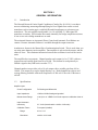
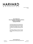
The Harvard Research
Carrier Signal Conditioner
User’s Manual
TABLE OF CONTENTS
SECTION
TITLE
I
GENERAL INFORMATION
II
III
PAGE
INTRODUCTION
1.1
SPECIFICATIONS
1.1
INSTALLATION
2.1
GENERAL
2.1
2.2
INITIAL INSPECTION
2.1
2.3
INSTALLATION
2.1
2.4
INPUT CONNECTIONS
2.1
2.5
POWER AND OUTPUT
2.2
2.6
PRELIMINARY SETUP
2.3
2.7
EXTENDING YOUR RANGE OF BALANCE
2.3
2.8
SIGNAL CABLE CONNECTIONS
2.3
2.9
PREAMPLIFIER POLARITY
2.4
2.10
THE LVDT
2.5
2.11
THE XX-XXXX ADAPTER ARM
2.5
2.12
OUTLINE DIMENSIONS
2.5
GENERAL
3.1
GENERAL
3.1
3.2
FRONT PANEL CONTROLS
3.1
3.3
INTERNAL CONTROLS
3.3
3.4
PLUG-IN COMPONENT TERMINALS
3.4
3.5
BRIDGE CALIBRATION
3.6
3.6
OPERATION
3.7
3.7
USING ZERO SUPPRESSION
3.7
3.8
OUTPUT – CHANNEL 2
3.7
3.9
FUNCTIONAL TEST PROCEDURE
3.8
LIST OF ILLUSTRATIONS
FIGURE
TITLE
PAGE
1–1
XX-XXXX CARRIER AMPLIFIER
1.1
2–1
REAR VIEW
2.1
2–2
INPUT CONNECTOR PIN CONNECTIONS
2.2
2–3
CARD EDGE CONNECTIONS
2.2
2–4
TYPICAL SIGNAL CONNECTIONS
2.4
2–5
PREAMPLIFIER POLARITY
2.5
2–6
SENSITIVITY CONTROLS
2.6
2–7
TYPICAL LVDT SIGNAL CONNECTIONS
2.6
2–8
XX-XXXX ADAPTER
2.7
2–9
OUTLINE DIMENSIONS
2.7
3–1
FRONT PANEL CONTROLS
3.2
3–2
INTERNAL CONTROLS
3.5
3–3
TEST INPUT CIRCUIT
3.8
SECTION I
GENERAL INFORMATION
1.1
Introduction
The Harvard Research Carrier Signal Conditioner (Catalog No. 60--0110), is our latest
answer to balancing, measuring and amplifying low level signals from carrier excited
transducers such as strain gages, variable differential transformers or reluctance type
transducers. The unit supplies an adjustable 1 to 10 volt RMS, 2.5 kHz signal for
transducer excitation. Provision has been made internally for bridge completion resistors
if one or two active bridge transducers are used.
The main unit features are Automatic Phase Control and Automatic Zero Balance on
comma. Remote Automatic Balance is available through the output connector.
Another new feature is the Master/Slave Synchronization Switch. This is used when you
are using more than one carrier amplifier. One amplifier is selected as the master, and the
others as slave. This eliminates interaction between the oscillators in each of the carrier
units.
The amplifier has two outputs. Channel number one's output is 0 to 5 VDC with zero
suppression and variable gain from 20 to 50,000. This channel is used primarily to
furnish a signal to the (2000 series recorder ????).
Channel number two provides a 0 to 10 volt output with a variable gain from 100 to
10,000. This output is set up for digital displays, etc. Both channels have direct and
average filtering available with corner frequencies of 200 or 0.05 Hz with 12 db/octave
roll-off.
1.2
Specifications
Amplifier Input:
Circuit Configuration
Full floating and differential
Input Impedance
1 M at 2.5 kHz floating and guarded
Measurement Range
±100 μV to ±1 V RMS for full scale output at a calibration factor of
1
Input Attenuator
Inaccuracy
X1, X100 (internal switch ± 0.25% of full scale)
Calibration Factor:
Front panel (duodial)
Range
0.5 to 10.5
Resolution
±0.05% of full scale
Non-Linearity
Auto Balance:
±0.25% of full scale
Front panel switch, indicator
Range
0 to ±10 mV RMS (R & C balance)
Resolution
11 bit with 18 k R bal resistor
Non-Linearity
±4 LSB out of 12 bit DAC
Remote Command
TTL compatible
Common Mode Rejection
> 120 dB at 60 Hz with 350 unbalance from input to chassis at
100 μV sensitivity
Leakage Current
< 10 μA RMS between any input terminal, including the
excitation, and chassis with 120 V RMS 60 Hz applied per UL544
Maximum Safe Voltage, Common Mode:
All 3000 and 5900
applications:
No off ground voltage allowed
IEC-601-1 applications
in 2000 recorders:
150 VDC or peak AC from the input terminals to chassis
IEC-348 applications
in 2000 recorders:
500 VDC or peak AC from the input terminals to chassis
Maximum Safe Voltage,
Normal Mode:
50 VDC or peak AC between input terminals
Terminals Provided
for (internal)
3 bridge completion resistors, 1 cal resistor and 1 zero balance
resistor
Instability:
Most sensitive scale (30 minute warm-up)
Zero–Time:
0.05% of full scale/24 hrs
Temperature
0.1% of full scale/°C
Line
0.1% of full scale/10% line variation
Gain-Time:
0.05% of reading/24 hrs
Temperature
0.08% of full scale/°C
Line
0.1% of full scale/10% line voltage change
Channel 1 Output:
Voltage:
0 to ±5 VDC into a 2 k load with 0.02 μfd capacitor or greater in
parallel
Impedance
< 5 (short protected)
Calibration Error
±0.1% of full scale
Non-Linearity
±0.1% of full scale
Noise
With 350 input unbalance and direct filter < 10 μV peak-topeak
Frequency Response:
Direct
DC to 200 Hz, 6 dB down at 200 Hz ±15%
Average
DC to 0.08 Hz, 6 dB down at 0.08 Hz ±20%; 12 dB/octave roll-off
Attenuator:
Steps
OFF, 1000, 500, 250, 100, 50, 25, 10
Inaccuracy
±0.25% between steps
Equivalent Input Signal
Short, 10, 5, 2.5, 1, 0.5, 0.25 and 0.1 mV at a calibration factor of
1
Sensitivity:
Range
> 2.5 to 1 variation also detent X1
Maximum Linear
Input Voltage
10 V RMS, sinusoidal at 2.5 kHz
Zero Suppression:
Range
±100 or ±1000 referred to the input
Resolution
±0.05% full scale
Non-Linearity
±0.25% full scale
Calibration
±0.1% independent of transducer phase
Channel 2 Output Voltage:
0 to ±10 VDC into a 2 k load with 0.02 μfd capacitor in parallel
Impedance
Same as channel 1
Calibration Error
Same as channel 1
Non-Linearity
±0.1% of full scale, X1 gain
Gain:
Internal switch; X1 to X10
X1 position
1 mV RMS input = 1 VDC output
X10 position
1 mV RMS input = 10 VDC output
Noise
Same as channel 1
Frequency Response
Same as channel 1
Instability
Same as channel 1
Direct-Average Filter
Internal switch; switch is overridden to direct position when the
front panel, Cal-Dir-Avg switch is placed in Cal position
Transducer Excitation:
Voltage Internally adjustable from 2 to 10 V RMS, maximum load 0.250 W
Frequency
2500 Hz ±5% sine wave
Total Harmonic Distortion
< 0.25% at 5 V RMS amplitude
Phase Demodulator
Automatic in-phase with signal
Synchronization
Jumper selectable, master to 7 slaves
Phase Reference
0° or 90°, internal switch selectable
Normal-Reverse
Internal switch selectable
Amplitude Instability:
With 30 minute warm-up
Time
±0.02%/24 hrs
Temperature
±0.1%/°C with 350 load
Line
±0.01%/10% line voltage change
Load Regulation
20% no load to full load with a 350 load
Power Requirements
+15 VDC at 125 mA
-15 VDC at 125 mA
13 VAC at 60 Hz at 200 mA
Accessories
11-5407-50
Mating Connector
11-5407-35
Transducer Adapter (Validyne, LVDT)
696238
Starter Kit
887291
Board Asm. Extender
R1-288308-13500
Resistor
242878-121
Resistor (Bridge)
242878-351
Resistor (Bridge)
25-265969-15001
Resistor (Balance)
25-265969-50001
Resistor (Balance)
SECTION II
INSTALLATION
2.1
General
This section describes the checks and inspections that should be made upon receiving
Harvard's 60-0110 Research Carrier Signal Conditioner. It covers installation, signal input
connections, and outline dimensions.
2.2
Initial Inspection
Prior to attempting any electrical connections or operation visually examine the unit for
broken or loose knobs, dented or nicked panels and broken or chipped rear connectors.
2.3
Installation
The 60-0110 Research Carrier Signal Conditioner may be mounted directly in Harvard's
Pressurized Ink and Thermal Pen Recorders, or Harvard's 8-, 4-, and
2-Channel Research Signal Conditioner Cases for use with other recorders.
2.3.1
Insertion
(Paragraph 2.6 Preliminary Set-Up must be completed before insertion)
To install the Signal Conditioner into the appropriate slot:
a.
Slide the Signal Conditioner into the enclosure until the rear output card
edge connector is engaged. See Figure 2-1 REAR VIEW
b.
Tighten the rear retaining screw until the Signal Conditioner front panel is
flush with the edge of the enclosure. Do Not Overtighten. This locks the
Signal Conditioner into the enclosure.
c.
Connect the input signal connector and secure it by grasping the rear of the
connector and pushing it onto the female connector after vertical alignment
of the blue index mark. When a click is heard or an orange ring appears, the
connector is locked in place.
2.3.2
Removal
a.
Disconnect the input connections with a counterclockwise turn to the
connector and pull.
b.
Loosen the rear retaining screw. The Signal Conditioner will move forward
abut 1/8 of an inch.
c.
2.4
Carefully slide the entire Signal Conditioner out of the recorder or signal
conditioner case.
Input Connections
Figure 2-2 shows the pin connections located at the rear of the Carrier Signal Conditioner.
For the convenience of the user, a mating guarded, 12-pin Deutsch Input Connector is
supplied (Catalog No. 60-0109). See Paragraph 2.8 for a typical wiring diagram.
PIN
FUNCTION
11
Signal (+)
12
Signal (-)
8
Excitation (-)
9
Excitation (+)
7
Shunt Cal.
10
2.5
Isolated Common
Power and Output
Output and power connections are made through a 16-pin card-edge connector. Refer to
Figure 2-3 for wired connections. These connections to the recorder are already made,
inside the system.
PIN
FUNCTION
1
* Common
2
Channel 1 Recorder Out
3
(-) 15 Volts
4
(+) 15 Volts
5
* Signal Common
6
Master/Slave Sync.
7
* Common 13 Volts AC
8
13 Volts AC
A
N.C.
B
Channel 1 Output
C
Remote auto-Balance Signal
D
N.C.
E
N.C.
F
N.C.
H
N.C.
J
Channel 2 Output
* Commons are tied on board to chassis ground.
2.5.1
Multi-Carrier Operation
Operating more than one Carrier in a system may require a synchronizing lead.
That is, pin 6 of all the carrier channels are wired together. One Carrier Signal
Conditioner is selected as master and the masterslave jumper is left at E4-E5 (see
Figure 3-2). All other amplifiers are considered slaves, and the jumper is moved to
E5-E6.
2.6
Preliminary Set-Up
2.6.1 – External Control Adjustment
Adjust the external controls to the following settings:
Control
Full Scale
Cal-Dir-Avg
Setting
OFF
Dir
Bal-ON-OFF
ON
Zero Suppression
OFF
Calibrate
Sensitivity
4
At detent (X1)
2.6.2 – Internal Control Adjustment
(Reference Sections 3.3 and 3.4) Remove right hand cover. Check for jumpers at
E1-E2 and E4-E5. Adjust the controls as follows:
Switch
Position
S1 (X100-X1)
X1
S2A (X1-x10)
X10
S2b (D-A)
D
S-3A (N-R)
N
S-3B (0-90)
0
2.6.3 – To Complete the Set-Up
Assuming your transducer is a 4 active element type, follow this set-up to
completion. If your si a 1 or 2 active element type, add bridge completion
resistors.
Install the Carrier Signal Conditioner in the proper channel.
Plug in the cable from the transducer you are going to use.
Make sure the transducer is in an at rest position (no load).
The excitation is set at the factor at 5 V RMS, with a load (see Section 5,
Calibration). If necessary, the excitation voltage can be set between 2 and 10 V
RMS by adjusting R-16 and monitoring TP-10 and 11.
Turn power on to the recorder and the Signal Conditioner.
Allow for a 15 minute warm up period.
Adjust the pen position to the center of the channel.
Turn the F.S. control to 1000.
Switch the Bal-ON-OFF switch to Bal. Hold momentarily.
The Phase light and then the Bal. light will glow and the pen will return to the
chart center.
Your system is now balanced.
If your system is unable to be balanced and oscillation will occur. The pen will
swing to the edge of the chart and then back towards the middle slowly (about 2
cps) but will not go to the center. If this indication occurs, see Note below.
NOTE: Your system will allow you to balance a 40 mV input (error) signal. This
figure is arrived at by multiplying the amplifier gain at 10 mV (with 18 k “R”
Balance Resistor) and the Calibrate setting of (4). If lower sensitivities are
required, a higher number can be adjusted on the Calibrate control, and/or X100X1 switch can be moved. Your total range of operation is from 10 mV to 10 V.
You can now change the FS attenuator to your desired sensitivity. Also the
calibrate control for proper amplification.
2.7
Extending Your Range of Balance
This Signal Conditioner has a gain of about 2.5 to 25 controlled by the front panel
calibration control. Figure 2-6 shows the controls used to change the sensitivity.
2.7.1
The Signal Conditioner, as stated, has an allowable 10 mV input signal range
because of the 18 k resistor in the R Balance position. If it is necessary to
increase the sensitivity to 1 mV we install a 1.3 k resistor, call for details.
The formula for computing the R balance resistor is:
45.54 e(in)
Rbal
=
0.035-e(in)
Where R bal is in k and e(in) is in volts. E(in) is the desired balance range and
should be limited to < 0.025 V.
You should remember that the higher the R balance resistance, the more coarse the
balance will be.
2.8
Signal Cable Connections
Use a four conductor, double foil, shielded signal cable Belden No. 8434, or equivalent.
The cable run from the transducer to Signal Conditioner should be one continuous length.
No Splices are Permitted, but mating low level signal connectors may be used if
necessary.
Connect the double shielded signal cable pair to the Signal Conditioner signal input
connector, pins 11 and 12.
Connect the shielded signal cable pair to the transducer excitation pins 8 and 9 as shown
in Figure 2-4.
Some bridges include a “shunt resistor” for use in calibration. If so, it should be
connected to pin 7 and a jumper must be placed in “Cal R” spot (see Figure 3-2). If Not,
Pin 7 Must Be jumpered to Pin 9 in the Input Connector. (Internal “Cal R“ will be
installed in Paragraph 3.5.)
Connect the signal cable shield to pin 10 located in the input connector and ground the
signal cable shield at the transducer as shown in Figure 2-4.
Note: The transducer enclosure should be grounded at the transducer.
It is important that the signal cable shield be insulated from the metal shell of the
preamplifier input connector. If this is not done “ground loop” noise will be created by
circulating currents in the signal cable shield between the transducer ground and the
preamplifier chassis ground.
2.9 Preamplifier Polarity
1.
When a POSITIVE signal is applied to a transducer we would expect the pen on
the recorder chart to move from chart center to the LEFT. To
accomplish this, the
transducer is connected as shown in Figure 2-4.
2.
Examination of Figure 2-5 will reveal that there is a polarity reversal
between the preamplifier input and output. This is done to compensate
polarity reversal that occurs in Harvard pendrive amplifiers.
3.
for the
POLARITY REVERSAL is accomplished by simply switching the internal
switch, (N-R) from Normal to Reverse. This switch inverts the oscillator output.
2.10 The LVDT
a.
A typical connection of an LVDT to the carrier preamplifier can be seen in
Figure 2-7. The center coil is the driven coil and obtains its signal from the
excitation output pins 8 and 9. The two pick-up coils are hooked in series
and sent to the input amplifier via input pins 11 and 12.
b.
The only change in set-up procedure, paragraph 2.6b, is the X100-X1
switch
is placed in the X100 position. The reason is, most LVDT’s have very high output,
usually in the volts range.
2.11 The 11-5407-35 Adapter Assembly
This Adapter, Figure 2-8, was designed to mate Validyne type transducers with the 134615-35 Carrier Amplifier. It will also reduce the carrier input signal by a factor of
approximately 20 to 1 to accommodate the relatively high Validyne transducer outputs.
2.12 Outline Dimensions
Preamplifier outline dimensions are shown in Figure 2-9.
SECTION III
OPERATION
3.1 General
This section describes and illustrates the controls of Carrier Amplifier models
13-4615-35. 13-G4615-35, and 20-4615-35, and provides complete operating
instructions.
3.2 Front Panel Controls
Item numbers listed below refer to circled numbers in Figure 3-1.
ITEM
CONTROL
DESCRIPTION
1
Full Scale Attenuator
(Channel 1) (S-101)
10 to 1000.
Sets the Full Scale output of
the amplifier in 7 steps from
2
Cal-Dir-Avg (S-102)
Direct for normal operation.
Average for normal operation.
Calibrate to obtain a deflection
change.
without a mechanical load
3
Bal-ON-OFF (S-103)
sets and locks the balance signal.
BAL – A momentary toggle; it
brings the balance and error
ON – for normal operation; it
signals together.
signal from the amplifier. Allows
OFF – removes only the balance
checking Phase Lock.
4
Zero Suppression (Channel 1)
+/-X100 switch (S-104)
±10 x 100 (1000% suppression)
A 5 position switch: OFF, ±1 x
100 (100% suppression) and
5
Vernier (R-102)
can be locked in any position.
major divisions. For use with
A ten-turn adjustable control that
The dial is graduated into 10
item 4.
6
Calibrate (Channels 1 and 2)
(R-103)
Set .5 to 10.5).
A 10-turn vernier resistor that
sets the overall gain (Gage factor
7
Sensitivity (Channel 1)
(R-104)
Provides a 25:1 Signal Change
A lockable variable resistor that
sets the gain of Channel 1 only.
from X1.
8
Trim Calibrate Resistor
(R-101)
amount of correction can be
switch.
This resistor is placed in series
with ”Cal R” so that a small
adjusted when using the Cal.
9
Bal Indicator (DS-102)
balancing of the amplifier. When
Green light is ON during the
”Bal” switch is activated.
10
Phase Indicator (DS-101)
excitation to signal phase shift
function of the internal switch
Yellow light goes on when the
exceeds ± 45° or ±90° as a
S3B.
3.3 Internal Controls
Item number listed below refer to those in Figure 3-2.
ITEM
CONTROL
DESCRIPTION
R-5
Gain Control Channel 2
Channel 2.
Adjustment to set the gain of
R-6
Zero Control Channel 1
Zero adjustment for Channel 1.
R-7
Phase Zero
amplifier.
Zero adjustment for the Phase
R-8
X10 Zero Suppression
X10 suppression circuit.
Calibration adjustment for the
R-9
X1 Zero Suppression
suppression circuit.
Calibration adjustment for the X1
R-10
Negative Zero Suppression
adjusted the negative component
Once the positive suppression is
is brought in with this
R-11
Quad Zero
adjustment.
Quadrature amplifier zero
R-13
Phase Balance
amplifier.
Balance control of the phase
R-14
Quad Balance
amplifier.
Balance control of the quadrature
R-15
Slave Phase
amplifier. Used to produce
Phase control of the Slave
2.5KHz signal for the bridge.
R-16
Excitation Span
oscillator.
Adjusts the output of the
R-17
Slave Balance
of the power supply for U-1
Balances the ripple component
against the oscillator output
the transducer.
R-82
Slave Zero
zero.
Balances U42 Slave Amplifier to
R-84
Input X100 CMR
position.
CMR adjustment in the X 100
R-85
Input X100 Gain
amplifier in the X100 position.
Gain adjustment of the input
R-88
Input X1 CMR
the first stage amplifier in the X1
CMR adjustment or balance of
position.
control.
to
R-89
Gain Control Channel 1
proper level.
Sets the gain of Channel 1 to its
S-1
Input Attenuator X1-X100
by 100 so instead of 10 to 1000 FS
This switch multiplies the input
we would have 1000 to
Channel 2 Gain X1-X10
only by a factor of 10.
This switch multiplies Channel 2
100K.
S-2A
3.3 Internal Controls (continued)
ITEM
CONTROL
DESCRIPTION
S-2B
Channel 2 Dir-Avg. Filter
Channel 2 in Dir or Avg mode
Channel 2 goes to Dir regardless
By this switch you can operate
independent of Channel 1.
when the Cal-Dir-Avg is
to Cal.
S-3A
Excitation Norm-Rev. Phase
switch reverses the phase of the
Just as the name implies, this
oscillator.
S-3B
Excitation 0 Degree – 90 Degree Phase
be 0 Degrees with resistive
Normal operation would
type Transducers.
other configurations a
necessary and
switched
For
Phase shift may be
is available.
3.4 Plug-In Component Terminals
Item numbers listed below refer to those on Figure 3-2.
ITEM
DESCRIPTION
R1-R2-R3
Bridge completion.
Cal R. (R-4)
Bridge Shunt Calibration.
Jumper
E1-E2 Normal
Calibration polarity reversal.
Jumper
E2-E3 Reverse
(Reverses calibration only).
Jumper
E4-E5 Master
be master, all others should be
Synchronization: One unit must
slave.
Jumper
E5-E6 Slave
+/-10mV offset (18Kohms).
Balance Resistor normally set for
3.4.1 Optional Filtering
For noisy environments a means of changing the filter frequency of 200 Hz.
(6 Db. down at 200 Hz. ± 15%) is provided. Both C-10 and C-11 must be
changed. Use Figure 3-2 to determine their location.
For Frequencies other than 200 Hz., C-10 and C-11 values may be calculated
using the following formula:
3.5 Bridge Calibration
After completing installation and setup instructions in Section 11, the unit may now be
calibrated. Three methods of calibration are used and are described below:
1.
Known calibration resistance (a given resistance equals a given mount of
micro-inches per inch, lbs/sq. inch, etc.).
2.
Transducer loading.
3.
Calculating calibration resistance.
mmHg,
All three methods will be described in detail. User must determine most convenient
method.
Note: If your bridge includes a “Shunt R” for calibration, just place a jumper in the “Cal
R” spot in the following steps.
1.
Known Calibration Resistance
a)
Install transducer.
b)
If calibration resistance is known, simply insert correct calibration resistor where
marked “CAL R”, and, if necessary, adjust the front panel trim
control for exact
resistance reading. (Internal Cal Resistor and the front
panel trim control are
additive. Part 3 below tells how to measure.)
c)
Turn “Full Scale” switch to 1000 and switch the “Bal-On-Off” switch to “Bal”
momentarily. This balances the Bridge.
d)
With resistance controls properly set, push “Cal-Dir-Avg” switch to “Cal”
position.
e)
Advance “Full Scale” control clockwise until desired Full Scale setting is
reached.
f)
Now adjust “Calibrate” control to place pen on desired chart division.
g)
Return “Cal” switch to “Dir”.
Example: For given transducer, 430K ohms equal 50mmHg. Install transducer and 430 K
ohm R CAL resistor. Turn the “Full Scale” switch to 1000 and switch the “Bal-On-Off”
switch to “Bal” momentarily. This balances the bridge. Turn “Cal-Dir-Avg”switch to
“Cal” position. Advance “Full Scale” to 100 position. Adjust “Calibrate” control to 50%
F.S. (25 divisions). Return toggle switch to“Dir” position. Each division on recorder
chart now represents 2mmHg.
2.
Transducer Loading
a)
If calibration resistance is unknown, it will be necessary to establish a
known
load or deflection at the transducer. Balance transducer per Section
2.6 and apply
a known load.
b)
Advance “Full Scale” to desired full scale setting.
c)
Now adjust “Calibrate” control to place pen on desired chart division and lock
control.
d)
Establish no-load condition at transducer.
e)
Set toggle switch to “Cal” position.
f)
Adjust internal CAL R and front panel “Trim” control until same pen
deflection is achieved.
g)
Record dial setting versus load or deflection and transducer number for
future
calibration reference. Also note total resistance. (Cal R and “Trim”
are in series in
the “Cal” position. Part 3 below tells how to measure.)
Example: For a typical transducer, apply a pressure of 100mmhg. Rotate “Full Scale” to
250 position. Adjust “Calibrate” control to set pen to 40% F.S. (20 division – 2VDC
output). Each chart division now represents 5mmHg. Vent transducer to air and push
toggle switch to “Cal” position. Adjust value of CAL R and front panel ”Trim” control
until same output is achieved. Note total resistance.
3.
Calculating Calibration Resistance
The proper calibration resistance (Rcal) can also be calculated using the following
equation:
R=
output resistance of transducer in ohms
F=
transducer calibration factor in microvolts (open circuit) per volt
per cmHg.
(excitation)
Example:
Determine the calibration resistance necessary to calibrate a Statham
P23 DB for 10 cmHg when given.
The calculated value is obtained by inserting a 1/4% resistor which is between the
calculated value minus 5K ohms. The front panel “Trim” control is then adjusted until
the desired resistance is achieved measuring across E1 and E3 with a precision ohmmeter.
CAL R and the TRIM pot are in series and the TRIM pot has a max R of 10K ohms.
3.6 Operation
Install the amplifier in its frame and properly lock it in place.
Turn the power on for warm up, approximately 15 minutes.
Connect the transducer to the input connector.
Turn the “Full Scale” control to Off and the “Bal-On-Off” switch to Off.
Calibrate control to 1.0 (unless otherwise determined). Sensitivity to X1-detent.
Zero suppression Off. “Cal-Dir-Avg” to “Dir”.
Turn on the chart drive and set pen position to chart center.
Switch “Bal-On-Off” to On.
Switch “Full Scale” to 1000. Now switch “Bal-On-Off” momentarily to “Bal”.
When the green and yellow lights go off, your unit is in balance. You may advance the
F.S. switch to a more appropriate sensitivity level. Your unit can now be “Cal”ed as in
Par. 3.5 and you will then be ready for operating.
3.7 Using Zero Suppression
Zero suppression permits the steady-state component of a complex signal (load) to be
suppressed allowing the dynamic portion to be amplified and recorded in greater detail.
a.
Set up the bridge as described in paragraph 3.5.
b.
Turn Zero Suppression “Vernier” to 1.00 (1 turn CW from full
counterclockwise position.)
c.
Apply a load to the strain gage and rotate the “Full Scale” control until the
pen approaches chart edge.
d.
Set the “Zero Suppression” (item 4) control to the appropriate range and
polarity. Pen should move back toward zero.
e.
Advance Zero Suppression “Vernier” dial clockwise until pen approaches chart
zero.
f.
Advance “Full Scale” control clockwise until desired sensitivity is reached,
keeping pen to chart zero with Xero Suppression “Vernier”.
g.
The load now may be varied around the static portion to obtain more
information.
useful
3.8 Output – Channel 2
Channel 2 was primarily designed to provide a signal for digital display and operates
regardless of the position of the attenuator. Its full scale output is 0 to
10 VDC and is located at pin J on the XA-201 output strip. With the use of switch
S-2A (internal) you can change the sensitivity of channel 2 by a factor of 10. With
1mVRMs input, the output will be 1 VDC in the x1 position, or 10 VDC in the x10
position. With switch S-2B you can change the output from direct (D) to average (A) DC
display.
3.9 Functional Test Procedure
This procedure should be performed to verify operation and calibration of the unit. If
calibration is required, refer to Section V of this manual.
1.
Connect two, 350 ohm resistors to the input connector as shown in Figure
3-3, below. Monitor channel 1 output (XA201-2) with a DMV.
2.
Set the “Calibrate” control, R103, fully CW and the “Full Scale” switch, S101,
to 1000. Set the “Sensitivity” control, R104, fully CW to the x1 position.
3.
Set the “Zero Suppression” switch, S104, to +10 and adjust the Zero
Suppression “Vernier”, R102, for a reading of .4.5 ±.001 VDC on the DVM
and lock it. Turn the “Zero Suppression” switch, S104, through its various
positions. The output on channel 1 should be shown below.
Zero Suppression
Switch
Channel 1
Output (VDC)
+10
+1
OFF
-1
-10
4.
-4.5 ± .001
-.45 ± .010
0 ± .010
+.45 ± .010
+4.5 ± .010
With the “Zero Suppression” switch, S104, set to -10, adjust the “Zero
Suppression” control, R102, as shown below and read channel 1 output to
check for linearity.
Zero Suppression
Switch
Channel 1
Output (VDC)
10.00
8.00
6.00
4.00
2.00
0.00
+5.0 ± .0075
+4.0 ± .025
+3.0 ± .025
+2.0 ± .025
+1.0 ± .025
0.0 ± .025
5.
Adjust the “Zero Suppression” control, R104, for a 2.5 ±.001 VDC reading
on the DVM and then change the “Full Scale” switch, S101, to 500. The output
on the DVM should change to 5.0 ±.02 VDC.
6.
7.
Repeat Step 5 for the other “Full Scale” switch settings, adjusting the “Zero
Suppression” switch and “Vernier” as shown below. The output should be
5.0 ±.02 VDC after switching to the next lower range.
Full
Scale Sw.
(Before)
1000
500
250
100
50
25
Suppression
Sw.
Output
Set
(Before)
Full
Scale Sw.
(After)
-10
-10
-10
-1
-1
-1
2.5 ± .001
2.5 ± .001
2.0 ± .001
2.5 ± .001
2.5 ± .001
2.0 ± .001
500
250
100
50
25
10
Remove input network and DVM.