Home
Explore
Baby & children
Computers & electronics
Entertainment & hobby
Fashion & style
Food, beverages & tobacco
Health & beauty
Home
Industrial & lab equipment
Office
Old
Pet care
Sports & recreation
Vehicles & accessories
Top types
Audio & home theatre
Cameras & camcorders
Computer cables
Computer components
Computers
Data input devices
Data storage
Networking
Print & Scan
Projectors
Smart wearables
Software
Telecom & navigation
TVs & monitors
Warranty & support
other →
Top brands
APC
Canon
Conceptronic
IBM
Sony
Targus
other →
Top types
Infotainment
Musical instruments
Video games & consoles
other →
Top brands
other →
Top types
Binding machines
Boards
Calculators
Correction media
Desk accessories & supplies
Drawing supplies
Equipment cleansing kit
Folders, binders & indexes
Laminators
Mail supplies
Paper cutters
Sorters
Storage accessories for office machines
Typewriters
Writing instruments
other →
Top brands
Belkin
Brother
Cables Direct
Canon
Casio
Fujitsu
HP
Kensington
Philips
Sharp
T'nB
Targus
Tripp Lite
Trust
V7
other →
Top types
Bedding & linens
Cleaning & disinfecting
Do-It-Yourself tools
Domestic appliances
Home décor
Home furniture
Home security & automation
Kitchen & houseware accessories
Kitchenware
Lighting
other →
Top brands
Baumatic
Bosch
Cuisinart
DeLonghi
Electrolux
Franke
Hama
Kenwood
KitchenAid
Miele
Panasonic
Philips
Siemens
Smeg
Tristar
other →
Top types
Bags & cases
Children carnival costumes
Clothing care
Clothing hangers
Dry cleaners
Fabric shavers
Men's clothing
Tie holders
Ultrasonic cleaning equipment
Watches
Women's clothing
other →
Top brands
Braun
Grundig
Irox
Mitsubishi Electric
Olympia
Omega
Philips
Sencor
SEVERIN
Shark
Solac
Termozeta
Timex
V7
Velleman
other →
Top types
Electrical equipment & supplies
Measuring, testing & control
Personal safety & protection
other →
Top brands
other →
Top types
Blood pressure units
Electric toothbrushes
Epilators
Feminine hygiene products
Foot baths
Hair trimmers & clippers
Makeup & manicure cases
Men's shavers
Personal paper products
Personal scales
Shaver accessories
Skin care
Solariums
Teeth care
Women's shavers
other →
Top brands
AEG
Audiovox
Black & Decker
Bosch
Hama
Honeywell
Kenmore
König
Panasonic
Philips
RCA
Rexel
SEVERIN
Siemens
Zanussi
other →
Top types
Hot beverage supplies
other →
Top brands
other →
Top types
Electric scooters
Motor vehicle accessories & components
Motor vehicle electronics
other →
Top brands
Razer
other →
Top types
Baby bathing & potting
Baby furniture
Baby safety
Baby sleeping & bedding
Baby travel
Feeding, diapering & nursing
Toys & accessories
other →
Top brands
other →
Top types
Bicycles & accessories
Bubble machines
Camping, tourism & outdoor
Fitness, gymnastics & weight training
Martial arts equipment
Skateboarding & skating
Smoke machines
Sport protective gear
Target & table games
Water sports equipment
Winter sports equipment
other →
Top brands
Chauvet
CHAUVET DJ
HQ Power
PROEL
other →
Top types
Pet hair clippers
other →
Top brands
Andis
other →
Top types
Baby Care
Computer equipment
Gadgets
Games
Home audio
Household appliances
Kitchen appliances
Lawn and Garden
Marine
Musical equipment
Personal care
Photography and Optics
Power tools
Sport & travel
Video and TV accessories
other →
Top brands
Acer
Asus
Canon
Cisco
Craftsman
Emerson
Epson
Makita
Miele
Motorola
Samsung
Sharp
Siemens
Whirlpool
Yamaha
other →
Upload
No category
Download
DatasheetDirect.com
1
2
3
4
5
6
7
8
9
10
11
12
13
14
15
16
17
18
19
20
21
22
23
24
25
26
27
28
29
30
31
32
33
34
35
36
37
38
39
40
41
42
43
44
45
46
47
48
49
50
51
52
53
54
55
56
57
58
59
60
61
62
63
64
65
66
67
68
69
70
71
72
73
74
75
76
77
78
79
80
81
82
83
84
85
86
87
88
89
90
91
92
93
94
95
96
97
98
99
100
101
102
103
104
105
106
107
108
109
110
111
112
113
114
115
116
117
118
119
120
121
122
123
124
125
126
127
128
129
130
131
132
133
134
135
136
137
138
139
140
141
142
143
144
145
146
147
148
149
150
151
152
153
154
155
156
157
158
159
160
161
162
163
164
165
166
167
168
169
170
171
172
173
174
175
176
177
178
179
180
181
182
183
184
185
186
187
188
189
190
191
192
193
194
195
196
197
198
199
200
201
202
203
204
205
206
207
208
209
210
211
212
213
214
215
216
217
218
219
220
221
222
223
224
225
226
227
228
229
230
231
232
233
234
235
236
237
238
239
240
241
242
243
244
245
246
247
248
249
250
251
252
253
254
255
256
257
258
259
260
261
262
263
264
265
266
267
268
269
270
271
272
273
274
275
276
277
278
279
280
281
282
283
284
285
286
287
288
289
290
291
292
293
294
295
296
297
298
299
300
301
302
303
304
305
306
307
308
309
310
311
312
313
314
315
316
317
318
319
320
321
322
323
324
325
326
327
328
329
330
331
332
333
334
335
336
337
338
339
340
341
342
343
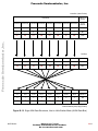
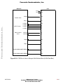
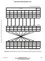
Transcript
Related documents
SC110 DSP Core Reference Manual
VAASAN AMMATTIKORKEAKOULU
Motorola MSC8101 ADS User`s guide
NAMC-ECAT_manual
An Approach in Nine Exercises
StarCore SC140 Application Development Tutorial
Manual
MC56F8013 Gang Programming
AN2450: Intializing Flash Memory for the MPC8260ADS
Full paper
MSC8102ADS - Freescale Semiconductor
Megawin 8051 ISP-ICP Programmer User Manual
CDQPrima 6.34 User's Manual
Freescale Semiconductor SC140 Computer Hardware User Manual
8051 ISP-ICP Programmer User Manual
PCI384
Megawin 8051 ISP
revising code designed for the eng board to also run on the pilot board
Megawin 8051 Writer
CodeWarrior™ Development Tools for StarCore DSP
Motorola ONCE SC140 User's Manual
56F8014 - NXP Semiconductors