1
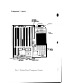
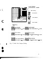
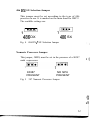
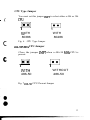
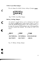
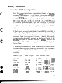
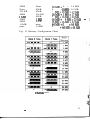
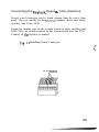
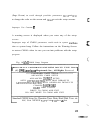
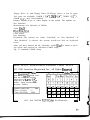
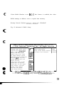
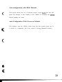
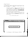
VESA
LOCAL BUS
3486
VL-BUS 3486
786 MINI-BOARD
USER’S MANUAL
Introduction ....................................................................2
Chapter 1 Main Features of System Board.. ....................3
Intel 486SX, 486DXf2,486DX, 386DX
Microprocessor ..................................................3
64 MB On-Board Main Memory.. ......................3
Secondary Cache Memory System .....................3
USA Integration Chip Set ..................................4
8 Fully Accessible Bus Slots ..............................7
Component Layout ................................8
Chapter 2 Hardware Configuration .................................9
Static Discharge Precautions 1. ............................9
Jumper Settings ..................................................9
Cache Memory Size Jumper .................. 10
486 DX/ SX Selection Jumper.. .............12
Numeric Processor Jumper ....................12
CPU Type Jumper .................................13
486-50 MHz CPU Jumper .....................13
CPU Clock Frequency Jumper.. .............14
VESA Local Bus Jumper .......................15
Battery Setting Jumper .......................... 15
Processor Installation .........................................16
Installing CPU .......................................16
Memory Installation........................................... 17
Available SIMM Configurations........... .17
InstaIling SIMMs ...................................19
Automatic Memory Sizing .....................19
Available Cache SRAM Configuration.. 20
Installing Cache SRAM .........................21
Chapter 3 Installation Guide ...........................................24
Static Discharge Precautions .1 ............................24
Installing The System Board ..............................24
Installing Power Connector ................................25
Connecting the Keylock, Reset & Turbo Switches 26I
Chapter 4 Using the BIOS Setup ................................... 21
1
The 786 AI0 system board is a “MINI” AT size, fully PC/AT
compatible motherboard with two 32 bit VESA standard Local Bus
slots, and the ability to use 486 or 386 microprocessor. It combines
the latest technology with design elegance unsurpassed by other
comparable system boards.
With a sophisticated secondary cache of 64 KB , 128 KB, or 256
KB high speed SRAM, and a maximum of 64 MB on-board main
memory, it is well suited for all high-end applications such as fileservers and advanced workstations.
The 786 AI0 system board incorporates the highly integrated USA
Integration chip set. System reliability is greatly enhanced by using
this chip set with few other discrete components.
The memory banks on the system board are located on the side of
the expansion slots. Full length cards can be installed in all expansion slots. Seven 16.bit expansion slots ( two with 32.bit Local
Bus socket ) and one 8-bit slot are provided.
Intel 486 DX, 486 DX/2,486 SX and 386DX microprocessors can
be used.
Other features include programmable bus speed, 2 programmable
non-cacheable areas and BIOS shadow RAM.
The system board is fully compatible with many operating environments including MS-DOS, Windows, UNIX, XENIX, OS/2 and the
NOVELL Netware Operating System.
2
CharHer 1 Main Features of Svstem Board
Intel 486SX, 486DX/2,486DX, 386DX Microprocessor
The Intel 486 microprocessor offers the highest performance possible for all operating systems and applications. Its one million
transistors integrate 8 KB of internal cache with a built-in cache
controller, floating-point coprocessor (except 486SX) and memory
management unit, while it remains fully compatible with 386DX
and SX microprocessors.
The Intel 486DX/2 clock-doubling microprocessor operates at the
maximum rated internal speed, while it interfaces with external
logics in half the internal clock rate. The DX/2 processor offers the
best price/performance ratio possible.
The 386 DX microprocessor has the same 32 bit addressing and
instruction capability, but it does not contain an internal cache or a
built-in floating point processor. It is an entry-level member the
486/386 family of microprocessors.
The 786AI0 Motherboard can utilize all the follow
microprocessors: 486 DX, 486DX/2,486 SX, and 386DX.
64 MB On-Board Main Memory
The 786 AI0 system board has 2 DRAM banks. Four types of
SWIMS are supported for up to 64 MB on-board memory: 256 KB
x 9,l MB x 9 ,4 MB x 9 and 16 MB x 9 SIMM modules, which
should satisfy even the most demanding applications.
Secondary Cache Memory System
To compliment the microprocessor’s internal cache, and to reduce
the need for main memory access, a secondary cache system is provided, utilizing 64 KB, 128 KB or 256 KB bytes of high speed
3
SRAhK The Secondary Cache System utilizes a Write-Back
Algorithm for optimum speed and performance.
Cache memory is used to store the most recently used instructions
or data. When the system is reset or powered-up, the cache memory
is empty. As the CPU reads data or instructions from the main
memory, this information is copied into the cache memory. Contents of cache memory are referenced by cache “‘tags” stored in high
speed SRAM tag memory. When an address is applied to access
data or instructions, the tags are compared with the address, and access to the contents of cache memory is granted if the tag and the
address match. This is called a cache hit. If they do not match, it is
called a cache miss, and a main memory read cycle is performed.
Since the typical access time of cache SRAM is about 20 to 25 ns,
compared to the 60 to 100 ns for main memory DRAM, cache
memory access is much faster. However, the actual increase in system performance depends on the nature of the software application.
Operation of the internal and secondary cache is transparent to the
user and to the software. When there are many more cache hits
than misses, the cache hit ratio is high. Memory access becomes
virtually immediate, and zero wait state memory access is achieved.
USA Integration Chip Set
The USA Integration chip set has the following features:
-Direct mapped organization with write-back protocol
-0 wait state for cache read / write hit
-Programmable cache read / write hit wait state.
Cache controller can be enabled or disabled
-Programmable cache line size
-Flexible cache size
-One or two bank of cache SRAM
-Flexible direct SRAM access mode
-Support for both hidden and conventional DRAM refresh
-Support for two independent non-cacheable regions
4
-Video and System BIOS Shadow RAM can be cacheable
in either the secondary cache or the 486 internal cache
-Support of fast Gate A20 operation for optimization of
OS / 2 operations
Support for Fast / Standard page mode DRAM
-Support for 2 banks of DRAM with memory size up to 64
MB
-Flexible system memory configurations
-Support mixable 256 KB x 9,1 MB x 9,4 MB x 9 , and 16
MB x 9 SIMM modules between banks
-Programmable DRAM wait state
Programmable cache flush
-Relocation of unused first 1 MB segments (128 KB, 256
KB, or 384 KB) to top of DRAM memory
-Automatic memory size detection
-CPU interface logic
-Data bus buffer control logic
-Reset and shutdown logic
-NM1 and port B support
-Feedback CPU clock to reduce clock skew
-Support for turbo / non-turbo mode
-Support for software turbo switch
-Support for conventional / hidden refresh
-Programmable bus clock
-DMA interface and arbitration logic
-Refresh address and control logic
-Data bus conversion logic
-Bus interface between different data buses
-Parity generation and checking logic
- 14.3 18Mhz and divide 12 counter
-AT Bus I/O recovery option for slower I/O cards
5
0
-_
130
PlrDW
PSE3N
IPBE2N
IP6ElN
PBEW
0
,.
X013
,
XDM
xDl5
’
KxJT2 h
OAEN6N &
OAENWI
ACXlB8
vDD13
VW
ADSTB16
SMEMWN
SMEMRN
OMWWN
OMEWW
KBDCW
GAlE2CN
DhUHDA
GATE2
RUWN
lUIA2W
moKN
CiMAN
-13
RTCAS
HRO
KSMTN
cwl
IOCW
8 Fully Accessible Bus Slots
The 786 AI0 system board has 7 standard 16.bit slots and 1
standard g-bit slots. Two of the 16 bit slots has VESA standard 32
-bit Local Bus expansion sockets. These slots accept all AT and
XT compatible expansion cards as well as VESA complient Local
Bus expansion cards.
The 16 bit expansion slots consists of parallel rows of pins which
match the connectors on the expansion cards. There are two
sections on the expansion slots: one long and one short. The long
sections are fully functional g-bit slots. Both sections are used
together to function as a 16.bit slot.
Local Bus slots are available on the two right-most expansion slots.
These two slots could accomodate g-bit, 16.bit or VESA Local Bus
32.bit expansion cards. Local Bus expansion cards bypass the
slower ISA Bus and communicate with the CPU Bus directly at the
maximum bandwidth of 66MHz (with 486 DX/2 66MHz
processor).
Since the memory banks are located on the right side of the
expansion slots, full length expansion cards can be used in all 8
slots without obstruction by the DRAM SIMMs.
Component Layout
OPTKNAL
E ERNALBATr.
“i
151 JMP3
8’
.
JMf’7 B
SIMM
SOCKETS
- CACHE
/ SRAMs
.
TURBO LED
KdLOCK
JtiP2
CACHE
JMP4 CONFIGURATION
JUMPER BLOCK
Fig. 2 System Board Component Layout
Chapter 2 Hardware Configuration
Static Discharge Precautions
!
,
Many components on the system board are sensitive to static
electricity. Special precautions must be taken when/ you handle the
system board to prevent damage. Discharge the static electricity on
your body by touching a grounded metal object, or by wearing a
grounded static wrist strap. Handle the system board by the edges
whenever possible. Avoid touching the surface on the system
board, and put the system board in a static-safe plastic bag before
transportation.
Jumper Settings
Jumper switches allow the user to choose among two or more
modes of operations. The switches have pins projecting from the
system board. A jumper cap is used to make connection between
two jumper pins. A jumper switch is closed when a jumper cap is
installed, and it is open when the pins are not connected by the
jumper cap.
Cache Memory Size Jumper
Two jumpers have to be set to choose the secondary cache
memory size: JMPl and JMP8.
Jumper JMPl has 3 rows of pins adjacent to each other.
JMPl has the following settings:
Jumper Setting
Cache Size
Memory Size
64 kBytes
64 kBytes
1 - <=16 MB
>16 - <=32 MB
128 kBytes
128 kBytes
1 - <=32 MB pins 2-3,4-5, 8-9 closed
>32 - <=64 MB pins 2-3,4-$7-8 closed
256 kBytes
256 kBytes
l-<=32MB
>32 - <=64 MB
pins l-2,4-5,7-8 closed
pins l-2,4-5,7-8 closed
pins 2-3,5-6, 8-9 closed
pins 2-3,5-6,7-8 closed
Jumper JMP8 has two rows of pins. It has the following
settings:
Cache Size
Jumper Setting
64 kBytes
pins
l-2 9
4-5
closed
128k Bytes
pins
2-3 9
4-5
closed
256k Bytes
pins
2-3 9
5-6
closed
I
,
.
0
0
CACHE MEMORY
CONFIGURATION JUMPER
.I 8
c,
/
JMP 8 Setting:
41
64 K CACHE
6 3
ki
1
1
128 K CACHE
0
256 k CACHE
JM Pl Setting:
MAIN MEMORY < = 16MB
16 MB < MAIN MEMORY < = 32 MB
963
128 K CACHE
MAIN MEMORY < = 32 MB
32 MB < MAIN MEMORY < = 64 MB
1
256 K CACHE MEMORY
MAIN MEMORY < = 32 MB
1
32 MB < MAIN MEMORY < = 64 MB
Fig. 3 Cache Size Jumper Setting
11
486 DX/ SX Selection Jumper
This jumper must be set according to the type of 486
processor in use. It is marked on the main board as JMP 2.
The available settings are:
486 DX
486 SX
Fig. 4 486 DX / SX Selection Jumper
Numeric Processor Jumper
This jumper, JMP4, must be set in the presence of a 80387
math coprocessor:
1
80387
PRESENT
NO NPU
PRESENT
Fig. 5 387 Numeric Processor Jumper
I
CPU Type Jumper
c
You must set this jumper JMPS to select either a 486 or 386
CPU:
ma
I
j/
ITH
80386
P
q
e
WITH
80486
Fig. 6 CPU Type Jumper
486-50 MHz CPU Jumper
Close the jumper JMP7 when a 486-50 MHz CPU is
present:
ra
-“-
ml.
1
WSTH
486-50
c----l
1
Ime
WITHOUT
486-50
Fig. 7 486-50 CPU Present Jumper
13
CPU Clock Frequency Jumper
Set this jumper JMP 9 according to the type of CPU
installed:
CPU
Jumper Closed
386/40
386133
386125
486DX/50
486DX/33,486DX2/66
486SX/25,486DX2,‘50
l-5,2-6
l-5,3-7,4-8
l-5,2-6,4-8
3-7
3-7,408
2-6,4-S
386/40
386133
386125
I::m:I
486DW50
486DW33
486DX2/66
486SXl25
486DXU50
Fig. 8 CPU Clock Frequency Jumper
VESA Local Bus Jumper
Do not change the default factory setting of jumper JMP 6.
10
6 woo 4
0.0 1
3
Fig. 9 VESA Local Bus Jumper
Battery Setting Jumper
An optional external battery can be attached to the board
via jumper pins 57. Battery setting jumper JMP3 is used to
select the built-in internal battery , the external battery, or
to erase the current CMOS setup in case of the its setting
becomes corrupt and unusable. The setting for JMP3 is as
below:
EXTERNAL INTERNAL DISCHARGE
BATTERY
BATTERY
CMOS
Fig. 10 Battery Setting Jumper
15
Processor Installation
Installing CPU
Special care should be taken when you install the CPU. It
should be installed only when the system board has not yet
been installed inside the system case. You should be aware
of possible static discharge causing damage to the CPU and
system board.
The system board should be laying on a flat surface facing
upward and be supported by a firm pad of foam or rubber.
Locate the CPU socket on the system board. The socket
has many holes which match the pins on the CPU itself. One comer of the socket is notched; this is the pin 1 comer
of the socket. The CPU has a notched pin 1 comer as well,
which is also indicated by a “dot” at that comer. Carefully
align the CPU with the socket so that the notched comers
are oriented in the same direction. Line up the pins on the
chip with the holes on the socket and press down firmly to
complete the installation.
t
l
I
Fig. 11 Intel 486 & 386 CPU
1
Memory Installation
Available SIMM Configurations
The 786 AI0 system board supports two banks of SWIMS.
Memory configuration is very simple due to the automatic
memory sizing and re-map feature of the system board. Up
to 64 MB of SIMMs may be installed. Different types (256
KBx9,1MBx9,4MBx9,16MBx9)ofSIMMsmay
be used for different banks, but only one type of memory
can be used in each bank. Each memory bank can be
disabled or ignored by setting the appropriate CMOS
register.
If the lowest memory bank (bank 0) has SIMMs installed, it
will be the logically lowest memory bank. However, the
system board automatically detects the logically lowest
memory bank for memory re-map, without having the
memory to be physically present on the lowest bank. If the
SWIMS on bank 0 are not present , SIMMs located on
memory bank 1 will be re-mapped to bank 0, the logically
lowest bank.
A memory bank must be filled completely in order for the
system board to work properly; therefore, the minimum
memory size is 1 MB. Up to 17 memory configurations are
possible:
Bank 0 Type
Bank 1 Type
Total Memory Size
256 KB
None
256 KB
1MB
None
256 KB
1MB
1MB
None
256 KB
256 KB
None
1MB
1MB
256 KB
1MB
1
0
1
4
0
1
4
4
MB+
0 = 1MB
+ lMB= 1MB
MB + lMB= 2MB
MB+
0 = 4MB
+ 4MB= 4 M B
MB+ 4MB= 5MB
MB+ 1 MB= 5MB
MB+4MB= 8 M B
17
4MB
None
256 KB
4MB
1MB
4MB
4MB
16MB
none
None
4MB
4MB
256 KB
4MB
1MB
4MB
none
16MB
16MB+ 0 = 1 6 M B
0
+ 16MB = 16 MB
1 MB+16MB=17MB
16MB+ lMB=l7MB
4 MB+16MB=20MB
16MB+
4MB=20MB
16MB+16MB=32MB
64MB+O
=64MB
0
+64MB=64MB
1
1;
Fig. 12 Memory Configuration Chart
Cl-
No SlMMs
installed
Jt
.
18
Installing SIMMs
Before installing or removing SWIMS on the system board,
turn off the power supply !
You should refer to Available SM.. Configuration to find
out the desired memory configuration. Make sure only
same type of SWIMS are used in each bank. SIMM
modules of different types are not allowed within the same
bank.
Whether Bank 0 only, Bank 1 only, or both memory banks
are installed, you should start the installation from the right
side of the board and proceed to the left (near the ISA
expansion slots).
A small hole is present on both ends of each SIMM. They
are used to snap the SIMM into the socket. Orient the
SIMM module such that the side without memory chips
faces the ISA expansion slots. Insert the SIMM firmly at
an 45 degree angle in the SIMM socket and push the SIMM
module down and to the right, towards the retaining arms of
the socket. The SIMM should gently snap into place.
Repeat the above process until the desired memory size is
reached.
Automatic Memory Sizing
Once the system is powered up, the BIOS automatically
determines how much memory is present in the system.
However, it needs to be configured before the system can
operate. Please refer to Chapter 4 - Using the BIOS setup
for more information.
19
Available Cache SRAM Configuration
Up to 2 banks of data cache SRAM are supported on the
486 ISA system board to give possible cache size of 64 KB,
128 KB, and 256 KB. The access time of the cache SRAM
must be 25 ns or better. Two types of SRAM are used to
achieve different cache sizes:
ata Cache Size
64 KB
128 KB
256 KB
four 8 KB x 8
four 32 KB x 8
four 32 KB x 8
Bank 1
four 8 KB x 8
four 32 KB x 8
Cache Banks are labeled on the system board as follows:
Cache Bank 0
Cache Bank 1
U18, U19, U20, and U21
U22, U23, U24, and U25
The corresponding SRAM Tag size is as follows:
Memorv Size SRAM Tag Size
Data Cache Size
1 - <=16MB
64 KB
8Kx8
>16 - <=32 MB
8Kx8 +16Kx4
64KB
128 KB
128 KB
1 - <=32 MB
>32 - <= 64 MB
8Kx8
8Kx8 + 16Kx4
256 KB
256 KB
1 -<= 32MB
>32 - <= 64 MB
32Kx8
32Kx8+16Kx4
The tag SRAM is located on the system board as U26 and
u 27.
Fig. 13 The SRAM
20
Installing Cache SRAM
If the 786 AI0 system board has SRAM installed already,
and you do not wish to alter the size of the Cache Memory,
please skip this section. Otherwise, we assume you are
installing cache SRAM on the system board for the first
time, or you wish to change the size of the cache memory.
Two types of SRAM (8 KB x 8 and 32 KB x 8) are used to
obtain different cache sizes. Correct cache size is obtained
by using the proper type of SRAM for the Cache Memory
AND the Cache Tag.
The Cache Tag stores the address of the information that is
located in the cache. Its function is similar to a look-up
table; the processor looks in the cache tag for the required
address, if the address is found, the corresponding cache
memory location is accessed. Otherwise, the main memory
is accessed.
Before procee,ding to installation, notice the following:
-Observe static discharge precautions!
-Timing requirements of the Cache Memory and the Cache
Tag are different. Access time of Cache Memory chips
should be equal to or less than 25 ns, and 20 ns or less for
the Cache Tag SRAM.
-Special toois may be required to remove the installed
SRAM chips from their sockets without causing damage.
If you are unsure of your ability to perform the
installation, you should have a trained technician perform
the iins~allation for you.
21
Identify the type of the SRAM chips already installed on
the board. Two types of chips are used: 8 KB x 8 and 32
KB x 8. The actual identification on the chips are quite
different and they are manufacturer dependant. Consult the
respective chip manufacturer’s hardware guide to detemline
the appropriate part required.
Two alternatives may be used to determine the current
cache memory size:
-If the system board is already installed in a complete
computer system, turn on the power and observe the
reported cache size on the screen. Remove the system
board from the case before proceeding to installation.
-Read the Cache Memory Jumper setting on the system
board, and the number of cache memory banks occupied.
Compare the jumper setting and the number of SRAM
banks occupied with Fig
Cache Memory Setting to
determine the current cache size.
The system board should be laying flat on a firm surface
facing upward, supported by a piece of foam or rubber.
Locate the SRAM sockets on the system board. Carefully
remove the installed SRAM chips if necessary.
Prepare the SRAM chips to be installed by orienting the
chips correctly as in Fig.1 3 Each chip has a notch on one
end, and it should match the notch on the socket where the
chip is to be installed.
Align the pins on the chip with the holes in the socket.
Press the chip down firmly. Inspect the pins on the chip to
make sure that none are bent.
Install each chip individually until the desired cache size is
reached.
22
Locate the cache memory jumper blocks JMPl and JMP8
on the system board.
Set the jumpers according to the installed cache size:
Data Cache Size
Memory Size SRAM TQ Size
64KB
1 - <=I6 MB
8Kx8
64KB
>16 - <=32 MB
8Kx8+16Kx4
128 KB
128 KB
1 - <=32 MB
>32 - <= 64 MB
8Kx8
8K%8+16Kx4
256 KB
256 KB
1 -<= 32MB
>32 - <= 64 MB
32Kx8
32Kx8+16Kx4
Verify the jumper settings with Fig 3 to complete the
installation.
23
Chapter 3 Installation Guide
Static Discharge Precautions
!
Many components on the system board are sensitive to static
electricity. Special precautions must be taken when you handle the
system board to prevent damage. Discharge static electricity on
your body by touching a grounded metal object, or by wearing a
grounded static wrist strap. Handle the system board by the edges
whenever possible. Avoid touching the surface on the system
board, and put the system board in a static-safe plastic bag before
transportation.
installing The System Board
If your system board has not yet been installed, follow the
instructions below to insure proper installation. Otherwise, you
may skip this chapter and proceed to the next.
The 786AI0 system board is designed to fit into many different
types of cases. Since it is not possible to cover all installation
situations, this chapter will illustrate the basic steps to install the
board in most common cases.
The system board has many drilled mounting holes. Some of which
line up with the mounting holes in the case. Mounting hardwares
such as plastic stand-offs, metal fasteners and screws are required to
secure the board inside the case.
You should use the mounting hardwares which came with the case
if possible to allow a better fit.
The locations to install the plastic stand-off on the system board
varies with the make and type of cases you use. You should use as
many stand-offs as the case will allow, to provide the system board
24
a good support in the case’s chassis, and to resist the downward
force from the expansion cards.
Try out the stand-off locations by aligning the system board with
the chassis of the system case.
Most. cases have several pre-drilled screw holes for metal fasteners.
Identify the proper locations to install the metal fasteners onto the
chassis. Two metal fasteners should be sufficient.
Snap on the plastic stand-offs on the system board from the bottom,
and gently lower the board inside the case. Line up the stand-offs
with the notches on the chassis and slide the board into place.
Carefully line up the board on the chassis such that the threads of
the metal fasteners are exposed inside the holes on the board.
Install the screws on the metal fasteners to complete the installation.
installing Power Connector
The system board draws power from the power supply through its
power connector. Most expansion cards also draw power from the
power supply indirectly through the AT expansion slots.
There are two power connectors from the power supply to the
system board. They are distinguishable only by the color of wires
which they are attached to. Extreme care should be taken to ensure
proper polarity. Severe damage to the system board could occur if
the position of the power connectors is incorrect.
A simple rule to instalI the power connectors:
Black colored ground wires should be in the middle of the
connector.
Locate the power connectors on the system board and connect them
to the power supply exactly as shown in Fig.\*
25
Connecting the Keylock, Reset 81 Turbo Switches
Several wired connectors can be found coming from the case’s front
panel. They are usually for the Keylock, Speaker, Reset and Turbo
switches, and Turbo LED.
Locate the jumper pins on the system board for these switches and
LED. They are clearly marked on the system board near the CPU.
Connect all tie switches as marked.
.
FG . 14 Installing Power Connector
BLACK WiRES
26
Chapter 4 Using the BIOS Setup
In this chapter we will explain the use of the BIOS setup program
from American. Megatrends Inc.
This setup program resides n the ROM BIOS and it is used to record system hardware settinge. If the system board has already been
installed and is functional, you do not need to alter the settings in
the CMOS Setup. If you are setting up the system board for the first
time, changing systm hardware configuration, or you have lost the
CMOS Setup due to battery drainage, the system board via the
BIOS setup program.
If you are settion up a new system board, the BIOS Setup program
is invoked automatically after Power On Self Test (POST). If an
error is encountered during POST, te system would notify the user in
two ways. If the display device (i.e. video Adapter) has not been initialized, a beep code is sent to the speaker. Otherwise, an error message is displayed on the screen. For non-fatal errors, you could
byapss the setup program by pressing the <Fl> key and allow to system to boot up from the floppy drive or hard drive.
The enter the CMOS setup, perform a system reset by one of the
following methods:
a. Turn off the power. Wait 10 seconds. Turn power back on.
b. Press the Reset Switch on the casz’s front panel.
c. Press (Del> keys simultaneously.
the follcwing message is displayed on the screen:
“Hit (Del>, if you want to run SETUP”
Press <Del> key immediately to enter the CMOS SETUP program.
Follow the instructions displayed to move around the different setup
screens. Use the arrow keys to switch fields. <Page Up> and
27
______l_______” _ “_____ _ -
. I ._
(Page Down) to scroll through possiblee parameters. (Fl> and <F3>
to change the color on the screen and <Et& to exit the setup screens.
Improper Use Caution !
A warning screen is displayed when you enter any of the setup
screens.
Improper setp of CMOS parameters could result in system malfunction or system hang. Follow the instructions on the Warning Screen
to restore CMOS values in case you run into problems with the setup
program.
Fig. 10 AMI BIOS Setup Program
(C) 1990 llmeriocan Megatrends Inc., All Rights Reserved
STANDARD CMOS SETUP
ADVANCED CMOS SETUP
ADVANCED CHIPSET SETUP
AUTO CNFIGURATION WITH BIOS DERAULTS
ART0 CONFTGURATION WITH OPWER-ON DEFAULTS
CHANGE PASSWOR-D
HAR.D DISK UTILITY
WRITE TO CMOS AND EXIT
DO ‘NOT WRITE TO CMOS AND EXIT
ESC; Exit XXXXX F2/F3 Color FlO: Save & Exit
28
,
Stanard CMOS Setup
Standard CMOS Setup records such information as date, time, hard
drive types and etc. As you enter the Standard CMOS Setup screen. A
small “Help Window” is displayed, showing a description of the current field and the acceptabl efi eld entries. the calendar and memory size
disp;ayed on the right side of screen are automatic.
The first twr lines in this screen records the date and time. Enter them
according to the format suggested in the, Help Window.
Daylight Savings--adds one hour to the CMOS time when daylight saving begins, and subtracts one hour when standard time returns.
Hard Disk C: and Hard Disk D: Type--type of hard disks prsent for
the first and second physical hard drives. Forty-seven types are possible
under AM1 BIOS. With the last type being an User Definable Types.
If no drives are present, choose “Not Installed”.
Drive type number 1-46 are pre-defined types. Please refer to Chapter
5: Technical Information--AM1 BIOS Hard Drive types for more information
Type 47 is a user definable type, the following information are needed
for each hard drive installed:
Clyn-Head-WPcom-Lzone-Size--
Number of cylinders.
Number of heads.
Write precom.
Landing zone of heads.
Capacity of drive, datermined automatically.
Notice that if yor are using a SCSI hard drive, the drive type should
be “not Installed”. If you are using an Intelligent IDE Controller or
ESDI the drive type should be “1”.
29
Floppy Drive A: and Floppy Drive B--Floppy drives A ans B types,
Fire types are available: 360KB 5 l/4”, 1.2MB 5 l/4”, 720KB 3 l/2”, 1.
44MB 3 l/2”, and “Not Installed”
Primary Display--Type of video display in the systim. The options are:
Not Installed
Monochrome (for Hercules of MDA)
Color 40x25
VGA/PGA/EGA
Color 80x25
Not Installed
Keyboard--The options are either “Installed” or “Not Installed”. If
“Not Installed” is chosen, the system would not halt on keyboard
errors.
After you have entered all the selections, oredd (Esc) to return to previous screen and opoceed to Advanced CMOS setup.
Fig. 11 Standard CMOS Setup
BIOS SETUP PROGRAM-STANDARD CMOS SETUP
(C) 1990 American Megatrends Inc., All Rights Recerved
Date (mm/date/year): Wed, Dee 26 1991
Time (hourlminlsec): 08: 09: 15
Hard disk C: type:47= USER TYPE
Hard disk D: type:Not Installed
Floppy drive A: I .2 MB, 5 l/4”
Floppy drive B: 1.44 MB, 3 l/2*
Primary display:VGA/PGA/EGA
Keyboard: Installed
Cylin Head Wpcom LZone Set Size MB
13
0
0
37
199
873
20
21
22
23
24
25 s 26
3
4
5
6
7
8
ESC: Exit XXXXX F2/F3:Color PU/PD:Modify
9
-
Advanced UMOS Setup
Advanced CMOS Setup csreen contains a list of systom features.
Some of which are urilized to fme tune systim performance. The default settings are listed in Figure 13.
Typematic Rate Programming--Control the rate at shich the system
can accept input from the keyboard. Default setting is “Disabled”.
Typematic Rte--Delay time for keyboard input. Options are 250ms,
SOOms, 750ms, and looms, Default setting is 500ms, 15 chars/set.
Above 1MB Memory Test--Default setting is “Enabled”.
Memory Parity Error Check--Test for errors during memory read. Default is “Enabled”.
Hit <Del> Message Display--Controls the screen prompt to access the
setup program. Default is <Enabled).
Hard Disk Type 47 RAM Area--Two options are available: 0;300 and
D O S 1KB. Option 0:300 places the hard disk type information at
RAM address 0:300, while DOS 1KB places them in the top 1KB of
the 640KB base memory. Default is “DOS 1KB”.
Wtit For <Fl) If Ang Error--System halts when error is encountered.
Resume operation wher <Fl> is pressed. Default is “Enabled”.
System Boot Up Mum Lock--Enables the numeric keys on the keypad
upon power up, instead of the regular arrow key functions, Default is
“On”.
31
Weitek Processsor--If installed, enable Weitek Processor by setting this
feature to “Present”. Default setting is “‘4bsent”.
System Boot Up Sequence--the default boot sequence is “C:;A:“, from
drive C: to drive A: It can be reversed to “A:$:“, from drive A: to drive C:.
System Boot Up CPU Speed--Default is ?3igh”.
Cache Memory controller--CPU Internal Cache Memory
Con troller enable. Default is “Enabled”.
Internal Cache Memory--Internal Cache Memory enable.
Default is “Enabled”.
Fast Gate A20 Option--Default is “Enabled”.
Password Check Option--This feature can becaused to prevent unauthorized system boot-up or unauthorized use of BIOS CMOS setup program. Two options are available:
1. “Always’‘--Prompt for password is displayed when the system is powered up.
2. “Setup’‘--Prompt for password is displayed when CMOS setyp program is accessed.
If enabled, the user has three attempts to enter the correct password.
After the third incorrect attempt, the system locks up and a reboot is
required.
To enable this feature, or to change the password, select the Change
Password option from the first setup screen.
32
Video ROM Shadow xxxx. i GK--IT this feature is enabled, the video
KOM starting at address xxxx is copied into memory.
Remap Unused Shadow memory--Default is “Disabled”.
Fig. 12 Advanced CMOS Setup
BIOS SETUP PROGRAM-ADVANCED CMOS SETUP
(C) 1990 American Megatrends Inc., All Rights Reserved
Typematic Rate Programming
Typematic Rate Delay (msec)
Typematic Rate (Chars/Set)
Above 1 MB Memory Test
Memory Test Tick Sound
Memory Parity Error Check
Hit [DEL] Message Display
Hard Disk Type 47 RAM Area
Wait For [Fl] If Any Error
System Boot Up Num Lock
Weitek Processor
Floppy Drive Seek At Boot
System Boot Up Sequence
System Boot Up CPU Speed
Cache Memory Controller
Internal Cache Memory
Fast Gate A20 Option
Turbo Switch Function
:Disabled
500
:15
:Disabled
:Enabled
:Enabled
:Enabled
:0:300
:Enabled
:On
:Absent
:Disabled
:C:,A:
:High
:Enabled
:Enabled
:Enabled
:Enabled
Password Checking Option’
Shadow RAM Option
Remap Unused Shadow MemoryBoot Sector Virus Protection
:
:
:
:
Setup
Both
Enablec
Enablec
------ESC:Exit XXXXX (Ctr!) Pu/Pd:Modify Fl :I-Iclp F2/F3:coior----.---F5:Old Values F6:BIOS Setup Defaults F7:PowerOon Dc6’;tu1ts------
33
Bus Frequency Select--This feature is used only if the CPU is driven
by its synchronous clock source “CLKIN” The actual bus clock
frequency is CLKIN divided by a factor of 4, 6, 8 or 10. Select the
proper speed according to the frequency of crystal used as CLKIN,
which is marked on the crystal next to the CPU socket. The resulting
bus clock frequency should not exceed 8.33M.H~.
CLKIN/x= Bus Clock Freq.
I/O Cyle Delay--Default is 250ns. Available options are Ons.
250ns, 500ns, 1000ns.
Refresh Methods--Memory Refresh Methods. Options are “Normal “
and “Hidden . Choose “Hidden” for faster performance.
Diagnostic Bits OxxH--Default setting is “0” .
Diagnostic Bits 03EH,(7,6)--Default setting is “1 n .
Diagnostic Bits 041H--Default setting is “0” ,If a 20MHz486SX is
used, change this value to “16))
Diagnostic bits 03DH--These Bits are used to program the CPU
speed in Non Turbo Mode. The smaller the value, the slower the
CPU speed Default setting is OCH.
Advanced CMOS Setup
Above 1 MB Memory Test--Default Setting
is “Disable”
For 50MHz:Cache read wait states is :l
:Cache write wait states is :l
:DRAM wait states is
:2
:BUS frequency select
:CLKIN/6
BIOS SETUP PROGRAM-ADflANCED
CHIPSET SETUP
(C)l990 American Megatrends Inc., All Rights Rewxved
Co-Processor Wait States
Cache Read Wait States
Cache Write Wait States
DRAM Wait States
Non-Cacheable Block 0 Size
Non-Cacheable Block 0
Non-Cacheable Block 1 Size
Non-Cacheable Block 1
Cache FOOO Shadow ROM, 64KB
486 Internal Cache, FOOO
486 Internal Cache, COO0
:o w/s
Keyboard Frequency Select
:l w / s
Bus Frequency Select
:l w / s
:2 w / s
I/O Cycle Delay
Refresh Method
:0 KB
:512 KB Parity Checking Method
:0 KB
Diagnostic bits 03EH, (7,6)
:512 KB Diagnostic bits 03FH, (7-O)
:Disabled
Diagnostic bits 041H, (7-O)
:Enabled Diabnostic bits 03DH, ( 7 - O )
:Enabled
:BUS CLK
:CLKIN/8
:250 nS
:Hidden
:Every
:o
:o
:o
:12
ESC:Exit XXXX (Ctrl) Pu/Pd:Modify Fl :Help F2/F3:color
, F5:Cld Walues F6:RIOS Setup Defaults F7:Power-on Defaults
34
Auto-configuration with BIOS Defaults
This option allows the use of default system values befor the user has
made any changes to the CMOS. If the CMOS is corrupted, the BIOS
default settings are used.
Auto-Configuration With Power-on Defaults
This features uses the CMOS values from the last system power up. It
is useful as a diagnostic aid if the system is having abnormal behavior.
Change Password
The Password-Check option is enabled when the system board is shipped. With default password “AMI” . The maximum length of password is 6 characters.
If Password is Enabled: To disable the password-check enter
a (return) character at the UNew Password” prompt and
press (return)again to confirm. To change the current password, enter the current password at YCurrent PasswordB
prompt. You will be asked to enter a new password. Enter
the new passowrd and press (return). Enter the password
again and press (return) to confirm the setup.
If Password is Disabled: To enable the password-check enter
a new password at the “New Password* prompt and press
(return). Enter the password again and press (return) to confirm the setup.
Fig. 14 Password Setup Screen
BIOS SETUP PROGRAM-CHANGE PASSWORD
(01990 American Menatrends Inc.. All Rights Reserved
Enter current password:
Use Maximum 6 ASCII Characters, ESC:Exit
36
Hard Disk Utillity
This utility is for MFM encoded hard drives only. It peroforms low-level formatting on Mfm HARD DRIVES. All the options in this utility
are data destructive, and they should be used only when low-level formatting is required.
1. Hard Disk Format--Perform low-level format on hard disk
2. Auto Inter leave--determines the optimum inter leave factor by measureing the transfer rate for four different inter leave values
prior to formatting.
3. Media Analysis--performs an analysis of each track of the hard drive
to determine whether it is usable. If the track is found unusable, it is marked as u bad” in the bad Track List Table.
IDE, ESDI, and SCSI hard drives cannot use the AMI BIOS hard
disk utility. Separate utilities are required for these drives.
Fig. 15 AMI BIOS Hard Disk Utility Screen
BIOS SETUP PROGRAM-HAARD DISK UTILITIES
(C)l990 American Megatrends Inc., All Rights Reserved
Cyln Head Wpcom LZone Sect Size(MB)
Hard Disk C: Type: 47USER TYPE 873 13 0 0 37 199
Hard Disk D: Type: Not Installed
Hard disk Type can be changed from the STANDARD CMOS SETUP
option in Main Menu
Hard Disk Format
Auto Interleave
Media Analysis
ESC:Exit XXXX F2/F3:Color
37
Write To CMOS And Exit
After the completion of all setups, choose Write To CMOS And Exit
to save the data and values changed. System reboots automaticaliy.
Do Not Write To CMOS And Exit
Abandon the BIOS Setup program and reboot system.
38