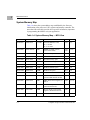
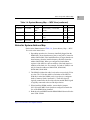
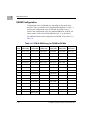
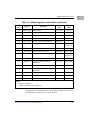
1
MBX Series Embedded Controller
Version C
Programmer’s Reference
Guide
MBXCA/PG1
December 2001 Edition
© Copyright 1997, 1998, 2001 Motorola Inc.
All rights reserved.
Printed in the United States of America.
Motorola® and the Motorola logo are registered trademarks of Motorola, Inc.
PowerQUICC™ is a trademark of Motorola, Inc.
PowerPC™ is a trademark of International Business Machines Corporation and is used by
Motorola with permission.
QSpan™ is a trademark of Tundra Semiconductor Corporation.
PC/104™ and PC/104-Plus™ are trademarks of the PC/104 Consortium.
I2C is a registered trademark of Philips Electronics.
All other products and/or services mentioned in this document may be trademarks or
registered trademarks of their respective holders.
Safety Summary
The following general safety precautions must be observed during all phases of operation, service, and repair of
this equipment. Failure to comply with these precautions or with specific warnings elsewhere in this manual
could result in personal injury or damage to the equipment.
The safety precautions listed below represent warnings of certain dangers of which Motorola is aware. You, as
the user of the product, should follow these warnings and all other safety precautions necessary for the safe
operation of the equipment in your operating environment.
Ground the Instrument.
To minimize shock hazard, the equipment chassis and enclosure must be connected to an electrical ground. If the
equipment is supplied with a three-conductor AC power cable, the power cable must be plugged into an approved
three-contact electrical outlet, with the grounding wire (green/yellow) reliably connected to an electrical ground
(safety ground) at the power outlet. The power jack and mating plug of the power cable meet International
Electrotechnical Commission (IEC) safety standards and local electrical regulatory codes.
Do Not Operate in an Explosive Atmosphere.
Do not operate the equipment in any explosive atmosphere such as in the presence of flammable gases or fumes.
Operation of any electrical equipment in such an environment could result in an explosion and cause injury or
damage.
Keep Away From Live Circuits Inside the Equipment.
Operating personnel must not remove equipment covers. Only Factory Authorized Service Personnel or other
qualified service personnel may remove equipment covers for internal subassembly or component replacement
or any internal adjustment. Service personnel should not replace components with power cable connected. Under
certain conditions, dangerous voltages may exist even with the power cable removed. To avoid injuries, such
personnel should always disconnect power and discharge circuits before touching components.
Use Caution When Exposing or Handling a CRT.
Breakage of a Cathode-Ray Tube (CRT) causes a high-velocity scattering of glass fragments (implosion). To
prevent CRT implosion, do not handle the CRT and avoid rough handling or jarring of the equipment. Handling
of a CRT should be done only by qualified service personnel using approved safety mask and gloves.
Do Not Substitute Parts or Modify Equipment.
Do not install substitute parts or perform any unauthorized modification of the equipment. Contact your local
Motorola representative for service and repair to ensure that all safety features are maintained.
Observe Warnings in Manual.
Warnings, such as the example below, precede potentially dangerous procedures throughout this manual.
Instructions contained in the warnings must be followed. You should also employ all other safety precautions
which you deem necessary for the operation of the equipment in your operating environment.
Warning
Warning
To prevent serious injury or death from dangerous voltages, use extreme
caution when handling, testing, and adjusting this equipment and its
components.
Flammability
All Motorola PWBs (printed wiring boards) are manufactured with a flammability rating
of 94V-0 by UL-recognized manufacturers.
EMI Caution
Caution
!
Caution
This equipment generates, uses and can radiate electromagnetic energy. It
may cause or be susceptible to electromagnetic interference (EMI) if not
installed and used with adequate EMI protection.
Lithium Battery Caution
This product contains a lithium battery to power the clock and calendar circuitry.
Caution
!
Caution
Caution
!
Attention
Caution
!
Vorsicht
Danger of explosion if battery is replaced incorrectly. Replace battery only
with the same or equivalent type recommended by the equipment
manufacturer. Dispose of used batteries according to the manufacturer’s
instructions.
Il y a danger d’explosion s’il y a remplacement incorrect de la batterie.
Remplacer uniquement avec une batterie du même type ou d’un type
équivalent recommandé par le constructeur. Mettre au rebut les batteries
usagées conformément aux instructions du fabricant.
Explosionsgefahr bei unsachgemäßem Austausch der Batterie. Ersatz nur
durch denselben oder einen vom Hersteller empfohlenen Typ. Entsorgung
gebrauchter Batterien nach Angaben des Herstellers.
CE Notice (European Community)
Motorola Computer Group products with the CE marking comply with the EMC Directive
(89/336/EEC). Compliance with this directive implies conformity to the following
European Norms:
EN55022 “Limits and Methods of Measurement of Radio Interference Characteristics
of Information Technology Equipment”; this product is tested to Equipment Class B
EN55024 “Information technology equipment—Immunity characteristics—Limits and
methods of measurement”
Board products are tested in a representative system to show compliance with the above
mentioned requirements. A proper installation in a CE-marked system will maintain the
required EMC/safety performance.
In accordance with European Community directives, a “Declaration of Conformity” has
been made and is available on request. Please contact your sales representative.
Notice
While reasonable efforts have been made to assure the accuracy of this document,
Motorola, Inc. assumes no liability resulting from any omissions in this document, or from
the use of the information obtained therein. Motorola reserves the right to revise this
document and to make changes from time to time in the content hereof without obligation
of Motorola to notify any person of such revision or changes.
Electronic versions of this material may be read online, downloaded for personal use, or
referenced in another document as a URL to the Motorola Computer Group Web site. The
text itself may not be published commercially in print or electronic form, edited, translated,
or otherwise altered without the permission of Motorola, Inc.
It is possible that this publication may contain reference to or information about Motorola
products (machines and programs), programming, or services that are not available in your
country. Such references or information must not be construed to mean that Motorola
intends to announce such Motorola products, programming, or services in your country.
Limited and Restricted Rights Legend
If the documentation contained herein is supplied, directly or indirectly, to the U.S.
Government, the following notice shall apply unless otherwise agreed to in writing by
Motorola, Inc.
Use, duplication, or disclosure by the Government is subject to restrictions as set forth in
subparagraph (b)(3) of the Rights in Technical Data clause at DFARS 252.227-7013 (Nov.
1995) and of the Rights in Noncommercial Computer Software and Documentation clause
at DFARS 252.227-7014 (Jun. 1995).
Motorola, Inc.
Computer Group
2900 South Diablo Way
Tempe, Arizona 85282
Contents
About This Book
Overview of Contents ................................................................................................xii
Comments and Suggestions ..................................................................................... xiii
Terminology ............................................................................................................. xiii
Conventions Used in This Manual .............................................................................xv
CHAPTER 1
MBX Initialization
Introduction .............................................................................................................. 1-1
Initialization Sequence ............................................................................................. 1-1
PowerPC Core ................................................................................................... 1-2
I2C/SPI Parameter RAM Patch ........................................................................ 1-3
System Interface Unit (SIU) Registers ............................................................. 1-4
Memory Controller ........................................................................................... 1-5
System Memory Map ........................................................................................ 1-8
Notes for System Address Map ........................................................................ 1-9
ISA Memory Map ............................................................................................1-11
DRAM Configuration ..................................................................................... 1-12
QSpan Initialization Values ............................................................................. 1-14
Winbond 83C554 Initialization Values ........................................................... 1-16
37C672 Peripheral I/O Device ............................................................................... 1-18
Required Interrupt Routing ............................................................................. 1-18
I/O Device Address Offsets ............................................................................ 1-20
I/O Device Configuration ............................................................................... 1-21
Interrupt Routing .................................................................................................... 1-24
Resets ..................................................................................................................... 1-26
Hardware Reset ............................................................................................... 1-26
Software Reset ................................................................................................ 1-27
CHAPTER 2
MPC8xx Multiple-Function Pins
Introduction .............................................................................................................. 2-1
Processor Bus Interface ............................................................................................ 2-1
PCMCIA and/or IPA Port Pins ......................................................................... 2-1
Interrupt Pins ..................................................................................................... 2-3
IPB Port Pins ..................................................................................................... 2-4
vii
Debug/IEEE 1149 Port Pins .............................................................................. 2-5
Miscellaneous Pins ............................................................................................ 2-5
Processor I/O Ports ................................................................................................... 2-7
Port A Pins — Definition vs. Function ............................................................. 2-7
Port B Pins — Definition vs. Function .............................................................. 2-8
Port C Pins — Definition vs. Function .............................................................. 2-9
Port D Pins — Definition vs. Function ........................................................... 2-10
CHAPTER 3
Additional Programming Information
Introduction .............................................................................................................. 3-1
Control and Status Registers ..................................................................................... 3-1
Control Register #1 ........................................................................................... 3-1
Status Register #1 .............................................................................................. 3-3
Control Register #2 ........................................................................................... 3-4
Status Register #2 .............................................................................................. 3-5
I2C Address Assignments ........................................................................................ 3-7
Digital Thermometer/Thermostat ............................................................................. 3-7
Utility Connectors ..................................................................................................... 3-8
Utility Connector #1 .......................................................................................... 3-8
Utility Connector #2 .......................................................................................... 3-9
APPENDIX A
NVRAM Map and EPPCBug
Overview ................................................................................................................. A-1
NVRAM Map ................................................................................................... A-2
Primary Network Configuration Parameters .................................................... A-4
CRC Calculation Routine ................................................................................. A-5
APPENDIX B
Related Documentation
MCG Documents ..................................................................................................... B-1
Manufacturers’ Documents ..................................................................................... B-2
Related Specifications ............................................................................................. B-3
GLOSSARY
viii
List of Tables
Table 1-1. Processor Core Configuration/Initialization .......................................... 1-2
Table 1-2. SIU Registers: Initial Values .................................................................. 1-4
Table 1-3. Memory Controller Register: Initial Values ........................................... 1-6
Table 1-4. System Memory Map — MPU View ..................................................... 1-8
Table 1-5. ISA Address Map ..................................................................................1-11
Table 1-6. UPM A RAM Array for DRAM at 50 MHz ........................................ 1-12
Table 1-7. Enhanced UPM A RAM Array for DRAM at 50 MHz ....................... 1-13
Table 1-8. QSpan Registers: Initial Values ............................................................ 1-14
Table 1-9. 83C554 Interrupt Initialization ............................................................. 1-17
Table 1-10. 37C672 I/O Device Interrupt Routing ................................................ 1-19
Table 1-11. 37C672 I/O Device Address Offsets .................................................. 1-20
Table 1-12. 37C672 I/O Device Configuration ..................................................... 1-21
Table 1-13. Interrupt Structure — ISA and PCI .................................................... 1-24
Table 1-14. Interrupt Structure — MPC8xx .......................................................... 1-25
Table 1-15. Hard Reset Configuration Word: Bit Definitions ............................... 1-27
Table 2-1. PCMCIA/IPA Port — Pin Definition vs. Function ................................ 2-2
Table 2-2. Interrupts — Pin Definition vs. Function ............................................... 2-3
Table 2-3. IPB Port — Pin Definition vs. Function ................................................ 2-4
Table 2-4. Debug/IEEE 1149 Port — Pin Definition vs. Function ......................... 2-5
Table 2-5. Miscellaneous Signals — Pin Definition vs. Function .......................... 2-6
Table 2-6. Peripheral Port A .................................................................................... 2-7
Table 2-7. Peripheral Port B .................................................................................... 2-8
Table 2-8. Peripheral Port C .................................................................................... 2-9
Table 2-9. Peripheral Port D ...................................................................................2-11
Table 3-1. Control Register #1: Bit Definitions ...................................................... 3-2
Table 3-2. Status Register #1: Bit Definitions ......................................................... 3-3
Table 3-3. Control Register #2: Bit Definitions ...................................................... 3-4
Table 3-4. Status Register #2: Bit Definitions ......................................................... 3-5
Table 3-5. I2C Address Assignments ...................................................................... 3-7
Table A-1. NVRAM Map ........................................................................................A-2
Table A-2. Primary Network Configuration Parameters .........................................A-4
Table B-1. Motorola Computer Group Documents .................................................B-1
Table B-2. Manufacturers’ Documents ...................................................................B-2
Table B-3. Related Specifications ...........................................................................B-3
ix
About This Book
The MBX Series Embedded Controller Version C Programmer’s Reference
Guide provides board-level information, complete memory maps, and
detailed chip information including register bit descriptions for the MBX
family of embedded controller boards. It is intended for use as a
companion to the MBX Series Embedded Controller Version C Installation
and Use manual listed under Motorola Computer Group Documents in
Appendix B, Related Documentation. This manual is intended for anyone
who wants to program these boards in order to design OEM systems, add
capability to an existing compatible system, or work in a lab environment
for experimental purposes. A knowledge of computers and digital logic is
assumed.
The information in this manual applies to MBX version C models in both
entry-level and standard configurations. The following table lists the
specific MBX models documented in this manual:
Model Number
Description
Entry-Level
MBX821-001C
50 MHz MPC821 processor, 4MB DRAM, 2MB Flash, 10BaseT Ethernet,
32KB NVRAM, COMM interface connector
MBX860-001C
50 MHz MPC860 processor, 4MB DRAM, 2MB Flash, 10BaseT Ethernet,
32KB NVRAM, COMM interface connector
Standard
MBX821 models include 50 MHz MPC821 processor; PC/104-Plus; 10BaseT Ethernet; EIDE
and Floppy interfaces; 32KB NVRAM; keyboard, mouse, IR, COM1 and COM2 ports; LCD
panel connector
MBX821-002C
4MB DRAM, 4MB Flash
MBX821-004C
16MB DRAM, 4MB Flash
MBX821-006C
16MB DRAM, 8MB Flash
xi
Model Number
Description
MBX860 models include 50 MHz MPC860 processor; PC/104-Plus; 10BaseT Ethernet; EIDE
and Floppy interfaces; 32KB NVRAM; keyboard, mouse, IR, COM1 and COM2 ports; COMM
interface connector
MBX860-002C
4MB DRAM, 4MB Flash
MBX860-004C
16MB DRAM, 4MB Flash
MBX860-006C
16MB DRAM, 8MB Flash
For programming reference information about other versions of the
MBX821 or MBX860, refer to the documentation that covers your model:
For MBX Model Numbers . . .
Refer to . . .
MBX821-00x, MBX860-00x
MBX Series Embedded Controller Programmer’s Reference
Guide (MBXA/PG1)
MBX821-00xA, MBX860-00xA
MBX Series Embedded Controller Programmer’s Reference
Guide (MBXA/PG1) and MBX Series version A customer
letter (MBXA/LT1)
MBX860-00xB
MBX Series Embedded Controller Version B Programmer’s
Reference Guide (MBXA/PG3)
Overview of Contents
This manual is divided into the chapters and appendices listed below.
❏ Chapter 1, MBX Initialization: Memory maps and guidelines for
initialization of the board.
❏ Chapter 2, MPC8xx Multiple-Function Pins: An examination of
the multiple-function pins on the MPC821 and MPC860
processors.
❏ Chapter 3, Additional Programming Information: A description of
various control and status registers on the MBX embedded
controller as well as the board’s I2C devices.
xii
❏ Appendix A, NVRAM Map and EPPCBug: A discussion of stored
data items that are pertinent to board configuration and operation.
❏ Appendix B, Related Documentation: A listing of other
publications that may be helpful in using the MBX board.
Comments and Suggestions
Motorola welcomes and appreciates your comments on its documentation.
We want to know what you think about our manuals and how we can make
them better. Mail comments to:
Motorola Computer Group
Reader Comments DW164
2900 S. Diablo Way
Tempe, Arizona 85282
You can also submit comments to the following e-mail address:
[email protected]
In all your correspondence, please list your name, position, and company.
Be sure to include the title and part number of the manual and tell how you
used it. Then tell us your feelings about its strengths and weaknesses and
any recommendations for improvements.
Terminology
Throughout this manual, a convention is used which precedes data and
address parameters by a character identifying the numeric format as
follows:
$
dollar
specifies a hexadecimal value
%
percent
specifies a binary number
&
ampersand
specifies a decimal number
For example, “&12” is the decimal number twelve, and “$12” is the
hexadecimal equivalent of the decimal number eighteen.
xiii
Unless otherwise specified, all address references are in hexadecimal
format.
A pound sign (#) or underscore-L (_L) following the signal name for
signals which are level significant denotes that the signal is true or valid
when the signal is low.
A pound sign (#) or underscore-L (_L) following the signal name for
signals which are edge significant denotes that the actions initiated by that
signal occur on high-to-low transitions.
In this manual, assertion and negation are used to specify forcing a signal
to a particular state. In particular, assertion and assert refer to a signal that
is active or true; negation and negate indicate a signal that is inactive or
false. These terms are used independently of the voltage level (high or low)
that they represent.
Data and address sizes for MPC8xx chips are defined as follows:
❏ A byte is eight bits, numbered 0 through 7, with bit 0 being the
most significant.
❏ A half-word is 16 bits, numbered 0 through 15, with bit 0 being the
most significant.
❏ A word or single word is 32 bits, numbered 0 through 31, with bit
0 being the most significant.
❏ A double word is 64 bits, numbered 0 through 63, with bit 0 being
the most significant.
Refer to the Endian Modes chapter in the PowerPC MPC821 Portable
Systems Microprocessor User’s Manual or MPC860 User’s Manual for
information on big-endian, small-endian, and PowerPC little-endian byte
ordering. For information on byte ordering in the PowerSpan PCI
interface, refer to the PowerSpan PowerPC-to-PCI Bus Switch Manual
listed in the Related Documentation appendix.
The terms control bit and status bit are used extensively in this document.
The term control bit describes a bit in a register that can be set and cleared
under software control. The term true indicates that a bit is in the state that
enables the function it controls. The term false indicates that the bit is in
the state that disables the function it controls. The terms 0 and 1 describe
xiv
the actual value that should be written to a bit, or the value that it yields
when read. The term status bit describes a bit in a register that reflects a
specific condition. The status bit can be read by software to determine
operational or exception conditions.
Conventions Used in This Manual
The following typographical conventions are used in this document:
bold
is used for user input that you type just as it appears; it is also used for
commands, options and arguments to commands, and names of
programs, directories and files.
italic
is used for names of variables to which you assign values, for function
parameters, and for structure names and fields. Italic is also used for
comments in screen displays and examples, and to introduce new
terms.
courier
is used for system output (for example, screen displays, reports),
examples, and system prompts.
<Enter>, <Return> or <CR>
represents the carriage return or Enter key.
Ctrl
represents the Control key. Execute control characters by pressing the
Ctrl key and the letter simultaneously, for example, Ctrl-d.
xv
1MBX Initialization
1
Introduction
This chapter details the default MBX initialization values as well as the
EPPCBug firmware initialization values. It is organized according to the
initialization hierarchy inherent in the hardware.
Initialization Sequence
At start-up or reset, the MPC8xx processor samples the data bus for initial
configuration based on current jumper settings and the design of the MBX
board. It then passes control to firmware for further initialization.
Initialization flows in a sequence determined by the hierarchy inherent in
the hardware:
1. MPC821/860 PowerPC core
2. MPC821/860 System Interface Unit (SIU)
3. MPC821/860 Memory Controller and memory
4. Primary PCI Bus Bridge device (Tundra QSpan chip; standard
configurations only)
5. ISA Bus Bridge device (Winbond W83C554F; standard
configurations only)
6. Super I/O device (Standard Microsystems Corporation 37C672;
standard configurations only)
7. PCI Address Spaces configuration and PCI Device configuration
(standard configurations only)
8. PCMCIA Module configuration
For further details on board initialization, you may also wish to review the
MBX Version C Installation and Use manual or the EPPCBug Firmware
Package User’s Manual listed in Appendix B, Related Documentation.
1-1
1
MBX Initialization
PowerPC Core
Within the processor chip is a module (the “core”) that embodies the
PowerPC architecture within the MPC8xx. Table 1-1 lists the firmware
initialization values for the principal control registers located within the
core.
Core registers not listed in the table either have indeterminate values or use
the processor default values. For more information, refer to the MPC821
or MPC860 processor manuals listed in Appendix B, Related
Documentation.
Table 1-1. Processor Core Configuration/Initialization
1-2
Special-Purpose
Register Value
Register
Mnemonic
Type
Firmware
Initialization
Value
&22
DEC
Supervisor
FFFF FFFF
&148
ICR
Debug
0000 0000
&149
DER
Debug
0000 0000
&158
ICTRL
Debug
0000 0000
&275
SPRG3
Supervisor
Reserved
&284
TB Write
Supervisor
0000 0000
&285
TBU Write
Supervisor
0000 0000
&560
IC_CST
Supervisor
0A00 0000
0400 0000
0C00 0000
0200 0000
Notes
1
2
Computer Group Literature Center Web Site
I2C/SPI Parameter RAM Patch
Table 1-1. Processor Core Configuration/Initialization (continued)
Firmware
Initialization
Value
Special-Purpose
Register Value
Register
Mnemonic
Type
&568
DC_CST
Supervisor
0A00 0000
0400 0000
0C00 0000
2
&638
IMMR
Supervisor
FA20 0000
3
—
MSR
Supervisor
0000 1002
Notes
Notes
1.
This register is reserved by the firmware.
2.
The series of values shown is written to cause invalidation of the code and data
cache.
3.
The firmware uses this register as a pointer to its internal data structures. When
system calls are made (the programmatic interface function) this register must
be restored to the same value at the time of client/target execution.
I2C/SPI Parameter RAM Patch
Due to an overlap in the parameter RAM of the MPC8xx processor,
I2C/SPI entries must be relocated in order to implement Ethernet (SCC1)
and I2C/SPI concurrently. Since IDMA1 is not used on the MBX, its
parameter RAM is reused for relocating the I2C.
EPPCBUG firmware downloads the MPC8xx I2C/SPI Microcode Package
and then relocates the I2C parameter RAM base to DPRAM_Base+$1CC0
(IDMA1 parameter base). Information about the microcode patch can be
found at:
http://www.mot.com/SPS/ADC/pps/subpgs/etoolbox/8XX/i2c_spi.html
http://www.motorola.com/computer/literature
1-3
1
1
MBX Initialization
System Interface Unit (SIU) Registers
Table 1-2 lists hardware initialization values used for SIU registers after
reset. For additional information about the state of the SIU Module
Configuration Register (SIUMCR) after reset, refer to the MPC821 or
MPC860 processor manuals listed in Appendix B, Related
Documentation.
Table 1-2. SIU Registers: Initial Values
Internal
Address
Register
Mnemonic
Register Name
MBX
Default
Value
Firmware
Initialization
Value
000
SIUMCR
SIU Module Configuration Register
006A 2900
0060 2900
004
SYPCR
System Protection Control Register
FFFF FF88
FFFF FF88
008
SWT
Software Watchdog Timer Current
Value
00E
SWSR
010
SIPEND
SIU Interrupt Pending Register
014
SIMASK
SIU Interrupt Mask Register
018
SIEL
01C
SIVEC
SIU Interrupt Vector Register
0000
020
TESR
Transfer Error Status Register
0001 0000
030
SDCR
SDMA Configuration Register
200
TBSCR
Timebase Status and Control
Register
0003
00C3
220
RTCSC
Real-Time Clock Status and Control
Register
00C3
00C3
240
PISCR
Periodic Interrupt Status and
Control Register
0083
0083
280
SCCR
System Clock Control Register
6200 0000
6200 0000
1-4
Software Service Register
SIU Interrupt Edge Level Mask
Register
AAAA 0000
FFFF FFFF
0000 0001
Computer Group Literature Center Web Site
Memory Controller
Table 1-2. SIU Registers: Initial Values (continued)
MBX
Default
Value
Firmware
Initialization
Value
0000 D000
0000 D000
Internal
Address
Register
Mnemonic
284
PLPRCR
PLL, Low Power and Reset Control
Register
320
RTCSCK
Real-Time Clock Status/Control
Register Key
55CC AA33
324
RTCK
Real-Time Clock Register Key
55CC AA33
328
RTCECK
Real-Time Alarm Seconds Key
55CC AA33
32C
RTCALK
Real-Time Alarm Register Key
55CC AA33
Register Name
Memory Controller
In hardware, all address decoding originates with the eight chip-select
banks of the memory controller incorporated into the MPC8xx processor.
Table 1-3 lists the initial values established by EPPCBug firmware for the
memory controller registers. Some values are dependent on the state of
jumper J4 (boot ROM device selection), the size of the on-board DRAM
memory, and the size of the optional DIMM memory.
Underlined values in Table 1-3 identify parameters required by the design
of the MBX board; they should not be modified. Other values are userselectable. For additional details about the processor Base and Option
registers, refer to the MPC821 or MPC860 processor manuals listed in
Appendix B, Related Documentation.
http://www.motorola.com/computer/literature
1-5
1
1
MBX Initialization
Table 1-3. Memory Controller Register: Initial Values
1-6
Offset
Mnemonic
Name
100
BR0
Base Register
Bank 0
104
OR0
Option Register
Bank 0
108
BR1
Base Register
Bank 1
10C
OR1
Option Register
Bank 1
110
BR2
Base Register
Bank 2
114
OR2
Option Register
Bank 2
118
BR3
Base Register
Bank 3
11C
OR3
Option Register
Bank 3
120
BR4
Base Register
Bank 4
124
OR4
Option Register
Bank 4
128
BR5
Base Register
Bank 5
12C
OR5
Option Register
Bank 5
130
BR6
Base Register
Bank 6
134
OR6
Option Register
Bank 6
Device
On-Board or
Socketed
Flash
Value
50MHz
Notes
FE00 0001
or
FC00 0401
1
FF80 0940
2
XXX0 0081
On-board
DRAM
XXX0 0400
DIMM
DRAM (Bank
0)
XXX0 0081
DIMM
DRAM (Bank
1)
XXX0 0081
NVRAM,
board-local
control/status
register spaces
FA00 0401
PCI I/O,
PCI memory
spaces
PCI Bus
bridge
registers
XXX0 0400
XXX0 0400
FFE0 0930
3
8000 0001
A000 0008
3
FA21 0001
FFFF 0108
3
Computer Group Literature Center Web Site
Memory Controller
Table 1-3. Memory Controller Register: Initial Values (continued)
Offset
Mnemonic
Name
138
BR7
Base Register
Bank 7
13C
OR7
Option Register
Bank 7
170
MAMR
Machine A
Mode Register
174
MBMR
Machine B
Mode Register
17A
MPTPR
Memory
Periodic Timer
Prescaler
Value
50MHz
Notes
FE00 0401
or
FC00 0001
1
FF80 0940
2
All DRAM
1880 1000
(no DIMM)
0880 1000
(DIMM
installed)
4
All DRAM
0200
Device
Socketed or
On-Board
Flash
Notes
1.
EPPCBug configures the reset Flash device at the lower address, and the
nonreset Flash device at the higher address, based on the setting of jumper
header J4 (boot ROM device selection).
2.
These initialization values assume 90ns or better access timing.
3.
These initialization values assume 70ns or better access timing.
4.
With a DIMM installed, the system has three banks of memory from a
hardware perspective: one soldered, and two on the DIMM. The refresh
periodic timer should be scaled back to 5µs so that the aggregate refresh time
comes to 15µs.
http://www.motorola.com/computer/literature
1-7
1
1
MBX Initialization
System Memory Map
Table 1-4 shows the system address map established by the firmware
initialization of the processor’s SIU registers and memory controller. The
notes that follow the table provide device-specific information, important
in programming the MBX to suit your application.
Table 1-4. System Memory Map — MPU View
Start
0000 0000
End
00XF FFFF
Size
4/16 MB
Definition
On-board DRAM (32 bit)
CS
Notes
CS1
1,4,7
X = 3 for 4M
X = F for 16M
00X0 0000
0XXX XXXX
x MB
DIMM slot (Bank 0 and 1)
(8/16/32/64/128M)
CS2
CS3
1,2,3,4
8000 0000
9FFF FFFF
512 MB
PCI/ISA I/O space
CS5
5,6,8,11
A000 0000
BFFF FFFF
512 MB
Reserved
C000 0000
DFFF FFFF
512 KB
PCI/ISA memory space
CS5
5,8,11
E000 0000
E3FF FFFF
64 MB
PCMCIA memory space
N/A
9,16
E400 0000
E7FF FFFF
64 MB
PCMCIA DMA memory space
N/A
9,16
E800 0000
EBFF FFFF
64 MB
PCMCIA attribute space
N/A
9,16
EC00 0000
EFFF FFFF
64 MB
PCMCIA I/O space
N/A
9,16
F000 0000
F9FF FFFF
160 MB
Unused
FA00 0000
FA0F FFFF
1 MB
NVRAM (BBSRAM; 8 bit)
(32/128/512K internal decode)
CS4
9,11
FA10 0000
FA1F FFFF
1 MB
MBX status/control registers #1
and #2
CS4
9,11,12
FA20 0000
FA20 FFFF
64 KB
MPC8xx dual-port RAM
(16K internal decode)
N/A
9
FA21 0000
FA21 FFFF
64 KB
PCI bus bridge control/status
registers (4K internal decode)
CS6
5,8
FA22 0000
FBFF FFFF
30592 KB
Unused
1-8
10
10
10
Computer Group Literature Center Web Site
Notes for System Address Map
Table 1-4. System Memory Map — MPU View (continued)
Start
End
Size
Definition
FC00 0000
FC7F FFFF
1/2/4/8
MB
Flash memory (1/2/4/8 MB;
32 bit)
FC80 0000
FDFF FFFF
24 MB
Reserved
FE00 0000
FE7F FFFF
8 MB
Boot ROM (128/256/512KB;
8 bit)
FE80 0000
FFFF FFFF
24 MB
Reserved
CS
Notes
CS0
CS7
7,13,14,
15
10
CS7
CS0
9,3,14,
15
10
Notes for System Address Map
Entries in the Notes column of Table 1-4, System Memory Map — MPU
View refer to the items below.
1. Depending upon the size of memory installed (plugged into the
DIMM slot), the on-board memory may or may not be located at
address $0000 0000. If the installed memory is larger than the onboard memory, then the installed memory should be located at
address $0000 0000. When you configure the bank address
registers of the MPC8xx, the base address of the bank must be a
modulus of the bank size. For example, if a bank is 32MB, it can
only be located at addresses $0000 0000, $0200 0000,
$0400 0000, $0600 0000.
2. The DIMM is 64 data bits wide, but it can be accessed only 32 bits
at a time. The 32-bit data width is a limitation of the MPC8xx.
With this in mind, the DIMM can be viewed as two contiguous
banks of memory (bank 0 and bank 1). The RAS0 signal is
logically connected to the first chip selection and the RAS2 signal
is logically connected to the second chip selection.
3. When installing DIMM modules, ensure that the jumpers
(J8/9/10) on the MBX Series board are configured to match the
size of the DIMM being installed.
4. Both the on-board DRAM and the DIMM DRAM share/utilize the
same UPM: UPMA.
http://www.motorola.com/computer/literature
1-9
1
1
MBX Initialization
5. The location of these address spaces is dependent upon the
presence of the PCI bus host bridge. PCI/ISA I/O space and
PCI/ISA memory space are programmable via the PCI bus host
bridge device (QSpan). On entry-level boards, CS5# and CS6# are
available at the 8xx/COMM expansion connector (P1) as well.
6. For details, see ISA Memory Map on page 1-11.
7. The size of these address spaces is queried from the I2C SROM
device.
8. The presence of the PCI bus host bridge device is queried from the
I2C SROM device.
9. These address spaces are smaller than the indicated size. The
actual decode is dependent upon the device. Address “wrapping”
may occur.
10. Access to any reserved/unused address space is undefined with
respect to boundaries. One cannot assume a behavior, predicted or
experienced, and any outcome is uncertain.
11. These address spaces share a common chip select; the specified
selection is further decoded by the appropriate address lines.
12. MBX control and status registers are byte addressed.
Control/Status Register #1 is located at all even addresses
$FA10 0000–$FA1F FFFE. Control/Status Register #2 is located
at all odd addresses $FA10 0001–$FA1F FFFF.
13. The MBX is designed to boot from either the on-board Flash or the
socketed Flash as determined by jumper J4, which variously
routes CS0# and CS7# to the two devices. The actual chip select
used is dependent upon the position of jumper J4. The MPC8xx
processor always uses CS0# as the source to the reset vector. By
default, the on-board Flash is on CS0# and the socketed Flash is at
CS7#.
After reset, CS0# is active for the entire memory. Software should
reconfigure to limit the range of CS0#.
1-10
Computer Group Literature Center Web Site
ISA Memory Map
14. EPPCBug can be executed from either the on-board Flash or the
socketed Flash. EPPCBug configures the reset Flash device at the
lower address, and the nonreset Flash device at the higher address.
Refer to the MBX Series Embedded Controller Version C
Installation and Use manual for information about selecting a boot
ROM device via jumper J4.
15. CS7# can alternatively be used for the 8xx/COMM expansion
connector (P1), if you boot from the 32-bit on-board Flash device
and the socketed Flash device is removed from XU1.
16. PCMCIA decodes are enabled only if a PCMCIA card is present
in the PCMCIA socket.
ISA Memory Map
Table 1-5 lists the firmware initialization values for the ISA address map
beginning at $80000000.
Table 1-5. ISA Address Map
Port
Description
ISA
Address
Enabled
FDC
Floppy disk controller
3F0–3F7
Y
UART1
Serial port 1
3F8–3FF
Y
UART2/IR
Serial port 2/Infrared
2F8–2FF
Y
Parallel
Parallel port
3BC–3BF
N
KBC
Keyboard controller
060, 064
Y
MOUSE
Mouse controller
060, 064
Y
Notes
1.
Base address of the peripheral I/O controller is $370 (the
alternate may be $3F0).
2.
Addresses are relocatable through software.
http://www.motorola.com/computer/literature
1-11
1
1
MBX Initialization
DRAM Configuration
Configuration values for DRAM vary depending on the speed of the
processor. They are stored in User Programmable Machine A. Table 1-6
specifies the configuration values for DRAM at 50 MHz. Table 1-7
specifies the configuration values for enhanced DRAM at 50 MHz. All
values assume 60 ns or faster EDO DRAM with 1, 2, or 4K refresh.
For additional details on the configuration of DRAM, refer to notes 1–4,
Table 1-4.
Table 1-6. UPM A RAM Array for DRAM at 50 MHz
Word
Single Read
(Offset $00)
Burst Read
(Offset $08)
Single Write
(Offset $18)
Burst Write
(Offset $20)
Refresh
(Offset $30)
Exception
(Offset $3C)
0
CFAF C004
CFAF C004
CFFF 0004
CFFF 0004
FCFF C004
FFFF C007
1
0FAF C404
0FAF C404
0FFF 0404
0FFF 0404
C0FF C004
2
0CAF 8C04
0CAF 8C04
0CFF 0C00
0CFF 0C00
01FF C004
3
10AF 0C04
00AF 0C04
13FF 4804
03FF 0C0C
0FFF C004
4
F0AF 0C00
07AF 0C08
FFFF C004
0CFF 0C00
1FFF C004
5
F3BF 4805
0CAF 0C04
FFFF C005
03FF 0C0C
FFFF C004
6
FFFF C005
01AF 0C04
0CFF 0C00
FFFF C005
7
0FAF 0C08
03FF 0C0C
8
0CAF 0C04
0CFF 0C00
9
01AF 0C04
13FF 4804
A
0FAF 0C08
FFFF C004
B
0CAF 0C04
FFFF C005
C
10AF 0C04
D
F0AF C000
E
F3BF 4805
F
FFFF C005
1-12
Computer Group Literature Center Web Site
DRAM Configuration
Table 1-7. Enhanced UPM A RAM Array for DRAM at 50 MHz
Word
Single Read
(Offset $00)
Burst Read
(Offset $08)
Single Write
(Offset $18)
Burst Write
(Offset $20)
Refresh
(Offset $30)
Exception
(Offset $3C)
0
CFEF C004
CFEF C004
CFFF 0004
CFFF 0004
FCFF C004
FFFF C007
1
0FAF C404
0FAF C404
0FFF 0404
0FFF 0404
C0FF C004
2
0CAF 0C04
0CAF 0C04
0CFF 0C00
0CFF 0C00
01FF C004
3
30AF 0C00
03AF 0C08
33FF 4804
03FF 0C0C
0FFF C004
4
F3BF 4805
0CAF 0C04
FFFF C005
0CFF 0C00
1FFF C004
5
03AF 0C08
03FF 0C0C
FFFF C004
6
0CAF 0C04
0CFF 0C00
FFFF C005
7
03AF 0C08
03FF 0C0C
8
0CAF 0C04
0CFF 0C00
9
30AF 0C00
33FF 4804
A
F3BF 4805
FFFF C004
B
0CAF 0C04
FFFF C005
C
D
E
F
http://www.motorola.com/computer/literature
1-13
1
1
MBX Initialization
QSpan Initialization Values
The QSpan R/W registers are initialized by firmware to the values listed in
Table 1-8. Read-only registers are left blank.
Table 1-8. QSpan Registers: Initial Values
Address
Offset
Register
000
PCI_ID
PCI Configuration Space ID
0860 10E3
004
PCI_CS
PCI Configuration Space Control
and Status
0280 0000
008
PCI_CLASS
PCI Configuration Class
0680 0000
00C
PCI_MISC0
PCI Configuration Miscellaneous 0
0000 0000
0000 0000
010
PCI_BSM
PCI Configuration Base Address
for Memory
xxxx x000
0100 0000
014
PCI_BSIO
PCI Configuration Base Address
for I/O
xxxx x001
1FFF F001
02C
PCI_SID
PCI Configuration Subsystem ID
xxxx xxxx
030
PCI_BSROM
PCI Configuration Expansion ROM
Base Address
0000 0000
0000 0000
03C
PCI_MISC1
PCI Configuration Miscellaneous 1
0000 0100
0000 0100
100
PBTI0_CTL
PCI Bus Target Image 0 Control
0000 0000
8F80 0080
(QSpan 1.2)
104
PBTI0_ADD
PCI Bus Target Image 0 Address
xxxx xxxx
8000 0000
110
PBTI1_CTL
PCI Bus Target Image 1 Control
0000 0000
0000 0000
114
PBTI1_ADD
PCI Bus Target Image 1 Address
xxxx xxxx
0000 0000
13C
PBROM_CTL
PCI Bus Expansion ROM Control
0000 0000
0000 0000
140
PB_ERRCS
PCI Bus Error Control and Status
0000 0070
8000 0000
144
PB_AERR
PCI Bus Address Error Log
0000 0000
148
PB_DERR
PCI Bus Data Error Log
0000 0000
400
IDMA_CS
IDMA Control and Status
0000 0000
1-14
Default
Value
Description
Initialization
Value
FB00 0147
0078 00081
Computer Group Literature Center Web Site
QSpan Initialization Values
Table 1-8. QSpan Registers: Initial Values (continued)
Address
Offset
Register
404
IDMA_ADD
IDMA Address
xxxx xxxx
Note 1
408
IDMA_CNT
IDMA Transfer Count
00xx xxxx
Note 1
500
CON_ADD
Configuration Address
0000 0000
Note 2
504
CON_DATA
Configuration Data
0000 0000
Note 2
508
IACK_GEN
IACK Cycle Generator Register
0000 0000
600
INT_STAT
Interrupt Status
0000 0000
EFF0 000F
(QSpan 1.2)
604
INT_CTL
Interrupt Control
0000 0000
0000 0000
608
INT_DIR
Interrupt Direction Control
0000 0000
0000 0000
800
MISC_CTL
Miscellaneous Control and Status
0000 0003
000C 0043
(QSpan 1.2)
F00
QBSI0_CTL
QBus Slave Image 0 Control
0000 0000
0100 0000
F04
QBSI0_AT
QBus Slave Image 0 Address
Translation
xxxx 00x0
0000 00D1
F10
QBSI1_CTL
QBus Slave Image 1 Control
0000 0000
0000 0000
F14
QBSI1_AT
QBus Slave Image 1 Address
Translation
xxxx 00x0
0000 00D1
F80
QB_ERRCS
QBus Error Log Control and Status
0000 0000
8100 0000
F84
QB_AERR
QBus Address Error Log
0000 0000
F88
QB_DERR
QBus Data Error
0000 0000
Description
Default
Value
Initialization
Value
Notes
1.
IDMA not supported.
2.
Variable depending on PCI peripherals.
The QSpan PCI Bus Bridge device can act either as master or as slave on
the local processor bus as well as on the PCI bus.
http://www.motorola.com/computer/literature
1-15
1
1
MBX Initialization
As a slave on the processor bus, the QSpan device can accept single-beat
or burst accesses from the processor. The GPCM (general-purpose chip
select machine) is used to interface to the QSpan; enabling the burst read
capability of the GPCM will enhance system performance.
As a master on the processor bus, the QSpan device performs memory
accesses to the area of memory controlled by the UPMA (userprogramable machine A). Due to the nature of the MPC8xx UPM memory
controller interface, the QSpan interface on the MPC8xx processor bus
cannot perform bursting in this case. The burst write feature should be
disabled.
QSpan register space is on chip select line CS6#. QSpan PCI space is on
CS5#. On entry-level boards, CS5# and CS6# are available at the
8xx/COMM expansion connector (P1) as well.
All accesses to the QSpan register space must be single-beat. The
programmer should mark this area noncacheable, to inhibit bursting to the
QSpan register space (see BR6 and OR6 in Table 1-3, Memory Controller
Register: Initial Values).
Accesses to the QSpan PCI memory space can be burst or single from the
processor perspective. To enable bursting to PCI memory space from the
processor, enable the burst bit in the BRn controlled by the GPCM (see
BR5 and OR5 in Table 1-3, Memory Controller Register: Initial Values).
Winbond 83C554 Initialization Values
The Winbond 83C554 PCI-to-ISA bridge register initialization values are
subject to change based on driver and application requirements. This
includes the support for application-specific EIDE-type devices. Interrupts
are defined in Table 1-13. For more information, refer to the EPPCBug
Firmware Package User’s Manual.
The 83C554 wakes up in an operational state. Initialization consists of:
❏ Programming the PCI interrupt routing registers
❏ Programming the interrupt edge/level detect registers
1-16
Computer Group Literature Center Web Site
Winbond 83C554 Initialization Values
❏ Setting up the three PC-type timers
❏ Programming the ISA bus control registers to a state conducive to
host operation
The Interrupt Controller portion of the 83C554 device is initialized by
firmware to the values listed in Table 1-9.
Table 1-9. 83C554 Interrupt Initialization
PRI
ISA
IRQ
PCI
IRQ
Contr.
Edge/
Level
INT1
Edge
High
Timer-0/Counter-0
Polarity
Interrupt Source
Notes
1
IRQ0
2
IRQ1
Edge
High
Keyboard
3-10
IRQ2
Edge
High
Cascaded Interrupt from
INT2
3
IRQ8
Edge
Low
4
IRQ9
Edge
Low
5
IRQ10
INTA#
Edge
Low
PCI Slot - INTA#
2,3
6
IRQ11
INTB#
Edge
Low
PCI Slot - INTB#
2,3
7
IRQ12
Edge
High
Mouse
8
IRQ13
Edge
High
9
IRQ14
INTC#
Edge
Low
PCI Slot - INTC#
2,3
10
IRQ15
INTD#
Edge
Low
PCI Slot - INTD#
2,3
INT2
http://www.motorola.com/computer/literature
1
1-17
1
1
MBX Initialization
Table 1-9. 83C554 Interrupt Initialization (continued)
PRI
ISA
IRQ
PCI
IRQ
Contr.
Edge/
Level
INT1
Polarity
Interrupt Source
Edge
High
COM2 (Async Serial Port #2)
COM1 (Async Serial Port #1)
11
IRQ3
12
IRQ4
Edge
High
13
IRQ5
Edge
High
14
IRQ6
Edge
High
Floppy
15
IRQ7
Edge
High
Parallel Port
Notes
Notes
1.
Internally generated by the 83C554.
2.
Initialize the PIRQ registers with the associated ISA IRQ value.
3.
The PIRQ values reside in NVRAM. These values are used upon a reset condition to initialize
the PIRQ registers located within the PCI-to-ISA bridge. This allows for a custom
initialization.
37C672 Peripheral I/O Device
The 37C672 I/O device is a collection of industry-standard PC I/O
peripherals (e.g., two UARTs, parallel port, FDC, keyboard/mouse
controller). The 37C672 peripheral I/O device register initialization values
are subject to change based upon driver and application requirements.
Required Interrupt Routing
The 37C672 device must be programmed to bring out the:
❏ Floppy Disk Controller (FDC) interrupt signal on pin 100, which
is defined as IRQ7 in the device. Pin 100 is then hardwired on the
board to ISA interrupt ISA_IRQ6.
❏ Keyboard interrupt signal on pin 97, which is defined as IRQ10 in
the device. Pin 97 is then hardwired on the board to ISA interrupt
ISA_IRQ1.
1-18
Computer Group Literature Center Web Site
Required Interrupt Routing
❏ Mouse interrupt signal on pin 92, which is defined as IRQ12 in the
device. Pin 92 is then hardwired on the board to ISA interrupt
ISA_IRQ12.
❏ Parallel port interrupt signal on pin 94, which is defined as IRQ11
in the device. Pin 94 is then hardwired on the board to ISA
interrupt ISA_IRQ7.
Table 1-10. 37C672 I/O Device Interrupt Routing
ISA IRQ
(Hardwired)
Function
Pin Number – Signal Name
Keyboard
Pin 97 - DSR#/SA15/ISA_IRQ10
ISA_IRQ1
COM2
Pin 33 - SER_IRQ/ISA_IRQ3
ISA_IRQ3
COM1
Pin 32 - PCI_CLK/ISA_IRQ4
ISA_IRQ4
FDC
Pin 100 - DTR#/SA14/ISA_IRQ7
ISA_IRQ6
Parallel Port
Pin 94 - DCD#/8042P12/ISA_IRQ11
ISA_IRQ7
Mouse
Pin 92 - RI#/8042P16/ISA_IRQ12
ISA_IRQ12
http://www.motorola.com/computer/literature
1-19
1
1
MBX Initialization
I/O Device Address Offsets
The 37C672 is plug-and-play (PnP) compatible. The PnP compatibility
requires that each of the I/O peripherals be located in the ISA address map
and that each of these address spaces be enabled.
To initialize the hardware, program each I/O peripheral’s base address
register and enable the address decode for it. Device initialization beyond
this occurs as needed by the specific device driver.
This is the same level of initialization that occurs with EPPCBug. Table
1-11 lists the I/O address offsets into PCI/ISA I/O space for the different
37C672 entities. These address offsets are a result of the firmware
initialization.
Table 1-11. 37C672 I/O Device Address Offsets
Resource
Enabled
Address
Mnemonic
Address
Offset(s)
Description
FDC
Yes
PRI
3F0-3F7
Floppy Disk Controller
Keyboard
Yes
COM1
3F8-3FF
Serial Port #1
Mouse
Yes
COM2
2F8-2FF
Serial Port #2
Parallel Port
Yes
LPTI
3BC-3BF
Parallel Port
KBC
Yes
060, 064
Keyboard/Mouse Controller
1-20
Computer Group Literature Center Web Site
I/O Device Configuration
I/O Device Configuration
Table 1-12 lists the firmware initialization values (in hexadecimal format)
for configuration-type registers of the 37C672. As previously stated, these
are just the initialization values. Operation of specific 37C672 drivers may
require additional initialization such as interrupt enabling, DMA
operations, operation modes/parameters, etc.
Table 1-12. 37C672 I/O Device Configuration
Index
Type
Configuration Register
Description
Hard Reset
Soft Reset
Initialization
Value
Global Configuration Registers
02
W
Configuration Control
00
00
03
R/W
Index Address
03
N/A
07
R/W
Logical Device Number
00
00
20
R
Device Identifier
40
40
21
R
Device Revision
01
01
22
R/W
Power Control
00
00
3F
23
R/W
Power Management
00
N/A
00
24
R/W
OSC
04
N/A
2B
R/W
Test 4
00
N/A
2C
R/W
Test 5
00
N/A
2D
R/W
Test 1
00
N/A
2E
R/W
Test 2
00
N/A
2F
R/W
Test 3
00
N/A
xx
Logical Device 0 Configuration Registers (FDD)
30
R/W
Activate
00
00
01
60
R/W
Primary Base I/O Address (15:8)
03
03
03
61
R/W
Primary Base I/O Address (7:0)
F0
F0
F0
70
R/W
Primary Interrupt Select
06
06
07
http://www.motorola.com/computer/literature
1-21
1
1
MBX Initialization
Table 1-12. 37C672 I/O Device Configuration (continued)
Configuration Register
Description
Hard Reset
Soft Reset
Initialization
Value
DMA Channel Select
02
02
02
R/W
FDD Mode Register
0E
N/A
06
F1
R/W
FDD Option Register
00
N/A
0C
F2
R/W
FDD Type Register
FF
N/A
55
F4
R/W
FDD0
00
N/A
01
F5
R/W
FDD1
00
N/A
01
Index
Type
74
R/W
F0
Logical Device 1 Configuration Registers (Reserved)
Logical Device 2 Configuration Registers (Reserved)
Logical Device 3 Configuration Registers (Parallel Port)
30
R/W
Activate
00
00
01
60
R/W
Primary Base I/O Address (15:8)
00
00
03
61
R/W
Primary Base I/O Address (7:0)
00
00
BC
70
R/W
Primary Interrupt Select
00
00
0B
74
R/W
DMA Channel Select
04
04
04
F0
R/W
Parallel Port Mode Register 1
3C
N/A
3C
F1
R/W
Parallel Port Mode Register 2
00
N/A
Logical Device 4 Configuration Registers (Serial Port 1)
30
R/W
Activate
00
00
01
60
R/W
Primary Base I/O Address (15:8)
00
00
03
61
R/W
Primary Base I/O Address (7:0)
00
00
F8
70
R/W
Primary Interrupt Select
00
00
04
F0
R/W
Serial Port 1 Mode Register
00
N/A
00
Logical Device 5 Configuration Registers (Serial Port 2)
30
R/W
Activate
00
00
01
60
R/W
Primary Base I/O Address (15:8)
00
00
02
1-22
Computer Group Literature Center Web Site
I/O Device Configuration
Table 1-12. 37C672 I/O Device Configuration (continued)
Index
Type
Configuration Register
Description
Hard Reset
Soft Reset
Initialization
Value
61
R/W
Primary Base I/O Address (7:0)
00
00
F8
62
R/W
Fast IR Base I/O Address (15:8)
00
00
63
R/W
Fast IR Base I/O Address (7:0)
00
00
70
R/W
Primary Interrupt Select
00
00
74
R/W
DMA Channel Select
04
04
F0
R/W
Serial Port 2 Mode Register
00
N/A
00
F1
R/W
IP Options Register
02
N/A
00
F2
R/W
IP Half-Duplex Timeout
03
N/A
03
Logical Device 6 Configuration Registers (Reserved)
Logical Device 7 Configuration Registers (Keyboard)
30
R/W
Activate
00
00
01
70
R/W
Primary Interrupt Select
00
00
0A
72
R/W
Secondary Interrupt Select
00
00
0C
F0
R/W
KRESET and GateA20 Select
00
N/A
Logical Device 8 Configuration Registers (Auxiliary I/O)
30
R/W
Activate
00
00
C0
R/W
Pin Multiplex Controls
00
N/A
http://www.motorola.com/computer/literature
00
1-23
1
MBX Initialization
Interrupt Routing
Table 1-13 and Table 1-14 present the interrupt structure of the MBX
Series embedded controller.
Table 1-13. Interrupt Structure — ISA and PCI
Source
F or S
ISA_IRQ0
Timer
F
ISA_IRQ1
Keyboard
F
ISA_IRQ2
Cascaded from ISA CNTLR #2
F
ISA_IRQ3
UART #2 / COM2
F
ISA_IRQ4
UART #1 / COM1
F
ISA_IRQ6
Floppy Disk
F
ISA_IRQ7
Parallel Port
F
ISA_IRQ10
PCI INTA (IDE)
S
ISA_IRQ11
PCI INTB
S
ISA_IRQ12
Mouse
F
ISA_IRQ5
ISA CONTROLLER #1
Interrupt
ISA_IRQ8
ISA_IRQ13
1-24
F
ISA_IRQ14
PCI INTC
S
ISA_IRQ15
PCI INTD
S
ISA_IRQA
S
ISA_IRQB
S
ISA_IRQC
S
ISA_IRQD
S
ISA CONTROLLER #2
Relocatable to any INT except 0,1,2,8, or 13
ISA_IRQ9
PCI
1
Computer Group Literature Center Web Site
Interrupt Routing
Table 1-14. Interrupt Structure — MPC8 xx
Interrupt
8xx_IRQ0
Source
Power Fail
LEVEL0
8xx_IRQ1
Temperature High/Low
QSpan
INTERNAL MPC8xx CONTROLLER
ISA CNTLR #1
Unavailable
S
Unavailable
LEVEL5
8xx_IRQ6
S
COMMINT_L
LEVEL6
8xx_IRQ7
F
S
LEVEL4
8xx_IRQ5
F
S
LEVEL3
8xx_IRQ4
F
S
LEVEL2
8xx_IRQ3
F
S
LEVEL1
8xx_IRQ2
F or S
F
S
Stop / Abort
LEVEL7
F
S
NMI
Watchdog Timer or IRQ
F
DEC
Decrementer
F
SIU
DEC, TB, PIT, RTC, PCMCIA
S
CPM
Port C Pins, Timers, SCCs, SMCs,
SPI, I2C, PIP, DMA
S
http://www.motorola.com/computer/literature
1-25
1
1
MBX Initialization
Notes
1.
S = Software configurable.
2.
F = Fixed hardware connection.
3.
TB, PIT, RTC, PIP, PCMCIA, and CPM_IRQ_Controller are all softwareconfigurable to any LEVELx.
4.
Watchdog Timer is configurable to generate NMI or HRESET.
5.
PCI interrupts and IDE interrupt are routable to any ISA interrupt except
0, 1, 2, 8, or 13. Default maps are A – 10, B – 11, C – 14, D – 15.
6.
For polarities, refer to Interrupt Pins on page 2-3.
Resets
To preserve the energy of the on-board battery, the battery will not supply
the processor keep-alive power (KAPWR) circuits until the board is first
placed in service.
When power is first applied to the MBX, the KAPWR supply is generally
below a minimum voltage threshold because of the “freshness seal” on the
battery. As a result, the reset circuitry on the board issues a power-on reset
(POR#) to the entire board, including the registers powered by the
KAPWR circuits.
The POR# signal also causes the MPC8xx processor to assert a hardware
reset (HRESET#) signal.
After this initialization, the freshness seal is broken and the battery always
supplies power to the processor KAPWR circuits when the main power is
removed. The processor never sees another POR# signal unless the battery
is removed and the main power disconnected.
Hardware Reset
The hardware reset (HRESET#) signal resets the entire system except the
portion of the processor powered by the KAPWR circuits.
When coming out of a hardware reset, the processor samples the data bus
for a hard reset configuration word. The configuration word is built in part
1-26
Computer Group Literature Center Web Site
Software Reset
from jumper settings; the jumpers should be set before you power up the
board.
The 32 bits that comprise the configuration word are defined in Table 1-15.
Table 1-15. Hard Reset Configuration Word: Bit Definitions
Bits
Definition
0-15
J100 0J01 0110 J000 (where J represents a jumper setting)
16-31
0000 0000 0000 0000 (reserved and must be zero)
Notes
1.
The jumper for bit position 0 (J6) specifies internal or external arbitration.
2.
The jumper for bit position 5 (J4) specifies a boot port size of 8 bits or 32 bits.
3.
The jumper for bit position 12 (J5) defines whether the DEBUG signals or the IEEE
1149 signals are active on the multiplexed DEBUG/IEEE1149 processor pins.
4.
The reset vector for the MPC8xx is set to 0000 0100 (IP=1, MSRIP=0).
5.
The Initial IMMR value is FF00 0000.
6.
The CLKOUT frequency is divided by 1 (EBDF=00).
The Power Monitor circuit monitors both +3.3V and +5V. At power-up, it
pulls HRESET# low until 350ms after both voltages reach their proper
operating levels. HRESET# is kept low (asserted) for as long as either
+3.3V or +5V is out of tolerance.
When the processor detects an HRESET# signal, it also drives SRESET#
low.
Software Reset
The software reset (SRESET#) signal is for use with an emulator or
debugger in development applications. SRESET# is present at pin 2 of the
MBX Debug connector (J24); it is routed to the MPC8xx SRESET# pin.
To enter Debug mode, SRESET# can be cleared to 0 while DSCK (pin 8
on the Debug connector) is set to 1. DSCK should remain set to 1 after
negation of SRESET# to enable the Debug mode immediately.
http://www.motorola.com/computer/literature
1-27
1
1
MBX Initialization
Note that the above is one of many ways to enter Debug mode. For further
information, refer to the appropriate processor manual or to the EPPCBug
Firmware Package User’s Manual listed in Appendix B, Related
Documentation.
1-28
Computer Group Literature Center Web Site
2MPC8xx
Multiple-Function Pins
2
Introduction
The MPC821 and MPC860 processors are highly integrated; a number of
pins serve multiple functions. Multi-function pins must be programmed in
accordance with the requirements of your application.
This chapter describes how the pins associated with the MPC821/860
processor bus interface and peripheral ports are multiplexed on the
MPMC8xx.
Processor Bus Interface
This section describes pins on the MPC8xx bus and control interface that
have multiple functions but have dedicated functionality. Programmable
pins must be set accordingly.
PCMCIA and/or IPA Port Pins
The PCMCIA interface signals for slot 1 are routed to the MPC8xx as
defined in Table 2-1. The MPC8xx IPA port is used for the PCMCIA slot
1 interface signals. The active-low signals (those with names followed by
a pound sign) can be defined as signals active on a low logic level or on the
falling edge.
2-1
MPC8xx Multiple-Function Pins
2
Table 2-1. PCMCIA/IPA Port — Pin Definition vs. Function
Processor
Pin Number
Pin Name
PCMCIA Function
T5
IPA0
VS1
T4
IPA1
VS2
U3
IPA2
WP or IOCS16#
W2
IPA3
CD2
U4
IPA4
CD1
U5
IPA5
BVD1 or SPKR
T6
IPA6
BVD2 or STSCHG
T3
IPA7
RDY or IRQ#
R3
WAITA#
WAIT#
L4
OP(0)
RESET
L2
OP(1)
PC Card Enable for Control
Signal Buffer
Alternate
DREQ#
DREQ#
The PCMCIA signal INPACK# is not needed for non-DMA type PCMCIA
cards in this design. To support PCMCIA cards that have DMA capability
and use the INPACK# pin for the DREQ# signal, a jumper (J11) on the
board enables you to connect the INPACK# signal to the IPA5 pin. For a
description of J11 functionality, refer to the MBX Series Embedded
Controller Version C Installation and Use manual listed under Motorola
Computer Group Documents in Appendix B, Related Documentation.
2-2
Computer Group Literature Center Web Site
Interrupt Pins
Interrupt Pins
2
The external interrupt pins available on the MPC8xx are defined in Table
2-2. The interrupt signals can be defined as active low or falling edge.
Table 2-2. Interrupts — Pin Definition vs. Function
Processor
Pin Number
Pin Name
Function
V14
8xx_IRQ0#
Power Fail Interrupt
U14
8xx_IRQ1#
Temperature Interrupt
H3
RSV# / 8xx_IRQ2#
8xx_IRQ2# as QSpan Interrupt
F2
CR# / 8xx_IRQ3#
8xx_IRQ3# as ISA Bus Interrupt
V5
DP1 / 8xx_IRQ4#
DP1 (IRQ4# unavailable)
W4
DP2 / 8xx_IRQ5#
DP2 (IRQ5# unavailable)
G3
FRZ / 8xx_IRQ6#
8xx_IRQ6# as 8xx/COMM Expansion Interrupt
W15
8xx_IRQ7#
Stop or Abort Interrupt
D18
PC14
User-selectable
E18
PC13
User-selectable
F18
PC12
User-selectable
L18
PC9
User-selectable
M18
PC8
User-selectable
M16
PC7
User-selectable
R19
PC6
User-selectable
T18
PC5
User-selectable
T17
PC4
User-selectable
External interrupt lines 4 and 5 are not available as interrupt lines (see
Miscellaneous Pins on page 2-5). All external interrupts feeding the
external interrupt pins of the MPC8xx are active low in polarity. The
8xx_IRQ1# interrupt (temperature interrupt) polarity is programmed in the
http://www.motorola.com/computer/literature
2-3
MPC8xx Multiple-Function Pins
digital thermometer and thermostat (DS1621S) device itself depending on
whether the interrupt is desired on a high temperature limit or a low
temperature limit. The MPC8xx allows for both level detection or edge
detection. For more information, refer to the EPPCBug Firmware Package
User’s Manual.
2
The Port C pins identified above can be redefined as interrupt lines to the
MPC8xx processor core when not used for another function/purpose. Each
available Port C pin, when configured as an interrupt signal, has a unique
interrupt vector as defined in Table 16-44 (Encoding the Interrupt Vector)
in the MPC860 User’s Manual and PowerPC MPC821 Portable Systems
Microprocessor User’s Manual. Making use of these pins involves tradeoffs with the other functionality they provide. See Port C Pins —
Definition vs. Function on page 2-9.
IPB Port Pins
The MPC8xx IPB(0:7) signals are defined in Table 2-3.
Table 2-3. IPB Port — Pin Definition vs. Function
Processor
2-4
Pin Number
Pin Name
Function
H2
IPB0 / IWP0 / VFLS0
VFLS0 (Debug Port)
J3
IPB1 / IWP1 / VFLS1
VFLS1 (Debug Port)
J2
IPB2 / IOIS16B# / AT2
AT2 (Unused)
G1
IPB3 / IWP2 / VF2
VF2 (No connection on board)
G2
IPB4 / IWP0 / VF0
VF0 (No connection on board)
J4
IPB5 / IWP1 / VF1
VF1 (No connection on board)
K3
IPB6 / DSDI / AT0
AT0 (Unused)
H1
IPB7 / PTR / AT3
AT3 (Unused)
Computer Group Literature Center Web Site
Debug/IEEE 1149 Port Pins
Debug/IEEE 1149 Port Pins
2
The MPC8xx Debug and/or Test Port pins are defined in Table 2-4.
Table 2-4. Debug/IEEE 1149 Port — Pin Definition vs.
Function
Processor
Pin Number
Pin Name
Function
H16
TCK / DSCK
If J5 1-2 then TCK
If J5 2-3 then DSCK
H17
TDI / DSDI
If J5 1-2 then TDI
If J5 2-3 then DSDI
G17
TDO / DSDO
If J5 1-2 then TDO
If J5 2-3 then DSDO
Note
Leaving J5 empty has the same effect as placing the jumper on
pins 2-3: it enables Debug functionality at the Debug header on
the board.
Miscellaneous Pins
A number of miscellaneous MPC8xx signals not covered in previous
sections are defined in Table 2-5. The active-low signals (those with names
followed by a pound sign) can be defined as signals active on a low logic
level or on the falling edge.
http://www.motorola.com/computer/literature
2-5
MPC8xx Multiple-Function Pins
2
Table 2-5. Miscellaneous Signals — Pin Definition vs. Function
Processor
Pin Number
Pin Name
Function
D2
BDIP/GPLB5#
BDIP
K1
KR#/RETRY#/8xx_IRQ4#/SPKROUT
RETRY#
H3
RSV#/8xx_IRQ2#
8xx_IRQ2#
F2
CR#/8xx_IRQ3#
8xx_IRQ3#
V3
DP0/8xx_IRQ3#
DP0
V5
DP1/8xx_IRQ4#
DP1
W4
DP2/8xx_IRQ5#
DP2
V4
DP3/8xx_IRQ6#
DP3
G3
FRZ/8xx_IRQ6#
8xx_IRQ6#
D5
CS6#/CE1B#
CS6#
C4
CS7#/CE2B#
CS7#
D7
GPLA0#/GPLB0#
DRAM Output Enable
C6
GPLA1#/GPLB1#
General Output Enable
B6
GPLA2#/GPLB2#
Unused and unconnected
C5
GPLA3#/GPLB3#
DRAM Buffer Output Enable
C1
UPWAITA/GPLA4#
Unused and unconnected
B1
UPWAITB/GPLB4#
Unused and unconnected
D3
GPLA5#/GPLB5#
DRAM Row/Column Selector
J1
ALEB/DSCK/AT1
AT1 (unused)
L1
OP2/MODCK1/STS#
MODCK1
M4
OP3/MODCK2/DSDO
MODCK2
M3
BADDR30/REG#
Unused and unconnected
2-6
Computer Group Literature Center Web Site
Processor I/O Ports
Processor I/O Ports
2
MPC8xx I/O Ports A B, C, and D have multiple functions but dedicated
functionality. In the following tables, “User selectable” means that any of
the signals listed under “Pin Name” are available for use. Wherever
applicable, the port pins must be programmed according to the tables
below.
Port A Pins — Definition vs. Function
The following tables list the pin assignments of the MPC8xx I/O ports with
respect to the processor pin name and the associated interface function.
Port A pins are defined in Table 2-6.
Table 2-6. Peripheral Port A
On
Header
Pin
Pin Name
Interface Function
C18
PA(15)/RXD1
SCC1_ETHERNET_RXD
No
D17
PA(14)/TXD1
SCC1_ETHERNET_TXD
No
E17
PA(13)/RXD2
SCC2_RXD
Yes
F17
PA(12)/TXD2
SCC2_TXD
Yes
G16
PA(11)/L1TXDb
User selectable
Yes
J17
PA(10)/L1RXDb
User selectable
Yes
K18
PA(9)/L1TXDa
User selectable
Yes
L17
PA(8)/L1RXDa
User selectable
Yes
M19
PA(7)/CLK1/TIN1/L1RCLKa/BRGO1
User selectable
Yes
M17
PA(6)/CLK2/TOUT1#/BRGCLK1
SCC1_ETHERNET_TCLK
No
N18
PA(5)/CLK3/TIN2/L1TCLKa/BRGOUT2
User selectable
Yes
P19
PA(4)/CLK4/TOUT4
SCC1_ETHERNET_RCLK
No
http://www.motorola.com/computer/literature
2-7
MPC8xx Multiple-Function Pins
Table 2-6. Peripheral Port A (continued)
2
On
Header
Pin
Pin Name
Interface Function
P17
PA(3)/CLK5/TIN3/BRGOUT3
User selectable
Yes
R18
PA(2)/CLK6/TOUT3#/L1RCLKb/BRGOUT2
User selectable
Yes
T19
PA(1)/CLK7/TIN4/BRGO4
User selectable
Yes
U19
PA(0)/CLK8/TOUT4#/L1TCLKb
User selectable
Yes
Port B Pins — Definition vs. Function
Port B is a dual-purpose port. If the MPC8xx parallel port is used, the Port
B pins function as described in the “Alternate Parallel Port” column in
Table 2-7. If the parallel port is not used, then the pins function as
described in the “Interface Function” column in Table 2-7. User-selectable
pins are routed to the 8xx/COMM expansion connector.
Table 2-7. Peripheral Port B
2-8
Pin
Pin Name
Interface
Function
Alternate
Parallel Port
On
Header
C17
PB(31)/SPISEL#/REJECT1#
User selectable
BUSY
Yes
C19
PB(30)/SPICLK
User selectable
SELECTOUT
Yes
E16
PB(29)/SPIMOSI
User selectable
PE or PERROR
Yes
D19
PB(28)/SPIMISO
User selectable
FAULT# or ERROR#
Yes
E19
PB(27)/I2CSDA/BRGO1
I2C_SDA
Yes
F19
PB(26)/I2CSCL/BRGO2
I2C_SCL
Yes
J16
PB(25)/SMTXD1
SMC1_TXD
Yes
J18
PB(24)/SMRXD1
SMC1_RXD
Yes
K17
PB(23)/SMSYN1#/SDACK1
User selectable
D0
Yes
L19
PB(22)/SMSYN2#/SDACK2
User selectable
D1
Yes
K16
PB(21)/SMTXD2/L1CLKOb
User selectable
D2
Yes
Computer Group Literature Center Web Site
Port C Pins — Definition vs. Function
Table 2-7. Peripheral Port B (continued)
2
Pin
Pin Name
Interface
Function
Alternate
Parallel Port
On
Header
L16
PB(20)/SMRXD2/L1CLKOa
User selectable
D3
Yes
N19
PB(19)/RTS1#/L1ST1
User selectable
D4
No
N17
PB(18)/RTS2#/L1ST2
User selectable
D5
No
P18
PB(17)/L1RQb/L1ST3
User selectable
D6
No
N16
PB(16)/L1RQa/L1ST4
User selectable
D7
No
R17
PB(15)/BRGO3
User selectable
STROBE_OUT#
No
U18
PB(14)/RSTRT1
User selectable
STROBE_IN#
No
The PB(25) and PB(24) signals are also routed to the 8xx/COMM
expansion connector and are available for general-purpose (userselectable) use if the on-board EIA-232 transceiver is disabled.
The I2C signals should be configured as open-drain type outputs. If you are
using the parallel port functionality of Port B, the appropriate parallel port
output signals should also be configured as open-drain type outputs.
Port C Pins — Definition vs. Function
Port C pins are described in Table 2-8.
Table 2-8. Peripheral Port C
Function
on MPC860
Function
on MPC821
On
Header
Pin
Pin Name
D16
PC(15)/DREQ1/RTS1#/L1ST1
SCC1_ETHERNET_TXEN#
No
D18
PC(14)/DREQ2/RTS2/L1ST2
SCC2_RTS#
Yes
E18
PC(13)/L1RQb/L1ST3
User selectable
Yes
F18
PC(12)/L1RQa/L1ST4
User selectable
Yes
J19
PC(11)/CTS1#
SCC1_ETHERNET_CLSN#
No
http://www.motorola.com/computer/literature
2-9
MPC8xx Multiple-Function Pins
Table 2-8. Peripheral Port C (continued)
2
Function
on MPC860
Pin
Pin Name
K19
PC(10)/CD1#/TGATE1#
L18
Function
on MPC821
On
Header
SCC1_ETHERNET_RXEN#
No
PC(9)/CTS2#
SCC2_CTS#
Yes
M18
PC(8)/CD2#/TGATE2#
SCC2_DCD#
Yes
M16
PC(7)/CTS3#/L1TSYNCb/SDACK2
SCC3_CTS#
User selectable
Yes
R19
PC(6)/CD2#/L1RSYNCb
SCC3_DCD#
User selectable
Yes
T18
PC(5)/CTS4#/L1TSYNCa/SDACK1
SCC4_CTS#
User selectable
Yes
T17
PC(4)/CD4#/L1RSYNCa
SCC4_DCD#
User selectable
Yes
Note
The SCC3 and SCC4 signals are not available on the MPC821.
Each of the SCC2, SCC3, and SCC4 signals listed above can be redefined
as “user selectable”. All of them are available on the 8xx/COMM
expansion connector.
In addition, all other Port C signals except PC15, PC11, and PC10 are
routed to the 8xx/COMM expansion connector. They may be redefined as
interrupt lines to the MPC8xx processor core when not in use for another
function/purpose. Each available Port C pin (when configured as an
interrupt signal) has a unique interrupt vector as defined in Table 16-44,
“Encoding the Interrupt Vector”, in the MPC860 User’s Manual and the
PowerPC MPC821 Portable Systems Microprocessor User’s Manual.
Port D Pins — Definition vs. Function
The Port D pins are described in Table 2-9. Port D is a dual-purpose port:
❏ MPC860. Port D is used for SCC3, SCC4, and several userselectable functions. All signals except PD(5:3) are routed to the
8xx/COMM expansion connector. Each of the SCC3 and SCC4
2-10
Computer Group Literature Center Web Site
Port D Pins — Definition vs. Function
signals listed in Table 2-9 may be redefined as “user selectable”.
All of them are available on the 8xx/COMM expansion connector.
❏ MPC821. All pins are reserved for an LCD interface. If no LCD
interface is used, then the PD(15:3) signals can serve as generalpurpose I/O lines. All signals except PD(5:3) are routed to the
8xx/COMM expansion connector.
Table 2-9. Peripheral Port D
Pin
Pin Name
Function
on MPC860
Function
on MPC821
On
Header
U17
PD(15) - L1TSYNCa or LD8
User selectable
LD8
Yes
V19
PD(14) - L1RSYNCa or LD7
User selectable
LD7
Yes
V18
PD(13) - L1TSYNCb or LD6
User selectable
LD6
Yes
R16
PD(12) - L1RSYNCb or LD5
User selectable
LD5
Yes
T16
PD(11) - RXD3 or LD4
SCC3_RXD
LD4
Yes
W18
PD(10) - TXD3 or LD3
SCC3_TXD
LD3
Yes
V17
PD(9) - RXD4 or LD2
SCC4_RXD
LD2
Yes
W17
PD(8) - TXD4 or LD1
SCC4_TXD
LD1
Yes
T15
PD(7) - RTS3# or LD0
SCC3_RTS#
LD0
Yes
V16
PD(6) - RTS4# or LCD_AC/OE
SCC4_RTS#
LCD_AC/OE
Yes
U15
PD(5) - REJECT2 or FRAME/VSYNC
User selectable
FRAME/VSYNC
Yes
U16
PD(4) - REJECT3 or LOAD/HSYNC
User selectable
LOAD/HSYNC
Yes
W16
PD(3) - REJECT4 or SHIFT/CLK
User selectable
SHIFT/CLK
Yes
Notes
1. The SCC3 and SCC4 signals are not available on the
MPC821.
2. LCD signals are not available on the MPC860.
http://www.motorola.com/computer/literature
2-11
2
MPC8xx Multiple-Function Pins
2
2-12
Computer Group Literature Center Web Site
3Additional Programming
Information
3
Introduction
This chapter describes various control and status registers on the MBX as
well as the board’s I2C address assignments and the DS1621 digital
thermometer and thermostat implementation.
Control and Status Registers
The MBX design includes two control and status registers. Both registers
are byte addressed. Control/Status Register #1 is located at all even
addresses $FA10 0000–$FA1F FFFE. Control/Status Register #2 is
located at all odd addresses $FA10 0001–$FA1F FFFF. Data lines 0
through 7 of the processor data bus connect to the respective registers, with
data line 0 carrying the most significant bit. The following sections define
the bits in those registers.
NVRAM and the control/status registers all share chip select signal CS4#.
PowerPC address line A11 distinguishes NVRAM from the control and
status registers.
Control Register #1
Control Register #1 sets and defines the configuration of the Ethernet Port
(bits 0 through 5) and the configuration of the on-board EIA-232-D serial
port transceiver (bits 6 and 7). The default setting of this register after reset
is $00. Firmware then initializes the register to $90 (entry-level boards) or
$92 (standard boards). The bits are defined in Table 3-2.
3-1
Additional Programming Information
Table 3-1. Control Register #1: Bit Definitions
3
Bit
0
Mnemonic
ETEN
Definition
0 = Disable Ethernet transceiver, Low Power mode
1 = Enable Ethernet transceiver
1
ELEN
0 = Disable Ethernet transceiver loopback capability
1 = Enable Ethernet transceiver internal loopback
2
EAEN
0 = Disable 10BaseT (TP) / AUI auto selection feature. Port selected
via bit 3.
1 = Enable auto selection of 10BaseT (TP) or AUI port
3
TPEN
This bit is functional only if bit 2 = 0.
0 = AUI port is manually selected
1= 10BaseT (TP) port is manually selected
4
FDDIS
This bit is functional only if the 10BaseT port is operational. Do not
enable if Loopback is enabled (bit 1 = 1).
0 = Enable Full Duplex mode of operation on 10BaseT port—
Disable Half Duplex
1 = Disable Full Duplex mode of operation—Enable Half Duplex
5
FCTEN
0 = Enable Forced Collision Testing on TP
1 = Disable Collision Testing capability on transceiver
6
COM1EN
(see Note)
This bit is irrelevant if the EIA-232 transceiver is disabled (bit 7 = 1).
0 = Route SMC1 communication signals to the EIA-232 transceiver
1 = Route COM1 communication signals to the EIA-232 transceiver
7
XCVRDIS
Setting this bit to 1 allows SMC1 to be utilized at the 8xx/COMM
interface.
0 = Enable on-board EIA-232 transceiver
1 = Disable the on-board EIA-232 transceiver, place it in Low Power
mode, and tri-state all transceiver outputs.
Note: On entry-level boards, bit 6 should be programmed to select SMC1. On standard
boards, program bit 6 to select COM1.
3-2
Computer Group Literature Center Web Site
Status Register #1
Status Register #1
Status Register #1 provides read-back capability of Control Register #1.
The bits are defined in Table 3-2.
Table 3-2. Status Register #1: Bit Definitions
Bit
0
Mnemonic
ETEN
Definition
0 = Ethernet transceiver disabled and in Low Power mode
1 = Ethernet transceiver enabled
1
ELEN
0 = Ethernet transceiver not looped back
1 = Ethernet transceiver in internal loopback
2
EAEN
0 = 10BaseT (TP) / AUI auto selection feature disabled.
1 = Auto selection of 10BaseT (TP) or AUI port enabled
3
TPEN
This bit is valid only if bit 2 = 0.
0 = AUI port is manually selected
1= 10BaseT (TP) port is manually selected
4
FDDIS
This bit is valid only if the 10BaseT port is operational.
0 = Full Duplex mode of operation on 10BaseT port enabled
1 = Full Duplex mode of operation on 10BaseT port disabled
5
FCTEN
0 = Forced Collision Testing on TP enabled
1 = Collision Testing on transceiver disabled
6
COM1EN
0 = SMC1 communication signals routed to the EIA-232 transceiver
1 = COM1 communication signals routed to the EIA-232 transceiver
7
XCVRDIS
Set to 1, this bit indicates that SMC1 can be utilized at the 8xx/COMM
interface.
0 = On-board EIA-232 transceiver enabled
1 = On-board EIA-232 transceiver disabled and in Low Power mode;
all transceiver outputs are tri-stated.
http://www.motorola.com/computer/literature
3-3
3
Additional Programming Information
Control Register #2
The first four bits in Control Register #2 (bits 0 through 3) set and define
the voltage requirements of the PCMCIA card that plugs into the on-board
PCMCIA socket. Bits 4 through 6 control status LEDs 4 through 6. When
Bit 7 is set, the processor has the ability to reset the PCI interface.
3
After reset, the default setting of this register is $00. If the board passes
startup diagnostics and a PCMCIA card is not installed, the register is
initialized by firmware to $0E. The bits are defined in Table 3-3.
Table 3-3. Control Register #2: Bit Definitions
Bit(s)
0 and 1
2 and 3
4
Mnemonic
VDDSEL(0:1)
VPPSEL(0:1)
BRDFAIL1
Definition
These two bits define the supply (Vcc or Vdd) voltage that is
presented to the PCMCIA card socket:
Bit 0
Bit 1
0
0
1
1
0
1
0
1
= Hi-Z
= +5.0V
= +3.3V
= Hi-Z
These two bits define the programming (Vpp) voltage that is
presented to the PCMCIA card socket:
Bit 0
Bit 1
0
0
0
1
1
1
0
1
= Ground
= +12.0V if bits 0 and 1 are 01 or 10,
Hi-Z if bits 0 and 1 are 00 or 11
= The value specified by bits 0 and 1 above
= Hi-Z
LED 4, orange:
0 = On (fail)
1 = Off (pass)
3-4
Computer Group Literature Center Web Site
Status Register #2
Table 3-3. Control Register #2: Bit Definitions (continued)
Bit(s)
Mnemonic
Definition
Battery Low1
5
3
LED 5, yellow:
0 = On
1= Off
6
7
Flash
Programming1,2
LED 6, yellow:
QSPANRST
0 = Normal operation, QSpan (host PCI bridge device) not reset.
1 = Reset QSpan (host PCI bridge device). PCI bus not reset.
0 = On
1 = Off
Notes
1.
The functions of LEDs 4, 5, and 6 respectively are defined and controlled in software through
these registers. The mnemonics for bits 4–6 represent the recommended configuration. These
bits may be used in other applications, however.
2.
Burst accesses to Flash memory are not supported.
Status Register #2
The first four bits in Status Register #2 (bits 0 through 3) are a read-back
of bits 0–3 in Control Register #2. The last four bits are defined in Table
3-4.
Table 3-4. Status Register #2: Bit Definitions
Bit(s)
0 and 1
Mnemonic
VDDSEL(0:1)
Definition
These two bits define the supply (Vcc or Vdd) voltage that is
presented to the PCMCIA card socket:
Bit 0
Bit 1
0
0
1
1
0
1
0
1
http://www.motorola.com/computer/literature
= Hi-Z
= +5.0V
= +3.3V
= Hi-Z
3-5
Additional Programming Information
Table 3-4. Status Register #2: Bit Definitions (continued)
Bit(s)
3
2 and 3
4
Mnemonic
VPPSEL(0:1)
BATGD
Definition
These two bits define the programming (Vpp) voltage that is
presented to the PCMCIA card socket:
Bit 0
Bit 1
0
0
0
1
1
1
0
1
= Ground
= +12.0V if bits 0 and 1 are 01 or 10,
Hi-Z if bits 0 and 1 are 00 or 11
= The voltage as specified by bits 0 and 1 above
= Hi-Z
Low battery voltage indication for the on-board or external backup
battery:
0 = Battery voltage is low. Battery requires replacement.
1 = Battery is good.
5
NVBATGD
Low Battery Voltage indication for the on-board battery-backed
SRAM (NVRAM):
0 = Battery voltage is low and NVRAM device should be replaced.
1= Battery voltage is good in the NVRAM device.
6
RDY/BSY#
Flash programming status bit. Valid only with Flash devices that
have a dedicated output pin to indicate programming status;
otherwise read as logical “1.”
0 = On-board Flash programming cycle not complete.
1 = On-board Flash programming cycle complete.
7
3-6
FT#
Reserved for factory test purposes.
Computer Group Literature Center Web Site
I2C Address Assignments
I2C Address Assignments
The MBX uses four of the 128 possible I2C connections. Table 3-5 lists the
address assignments (in hexadecimal format) for the devices implemented.
These I2C signals are also routed to the 8xx/COMM connector.
Table 3-5. I2C Address Assignments
Write
Address
Read
Address
A4
A5
A6
A7
DIMM (Serial Presence Detect)
A2
A3
Reserved
A8
A9
Digital Thermometer and Thermostat
90
91
Device
Board configuration EEPROM
Note: The Board Configuration serial EEPROM is
partitioned in two halves. The first half responds to addresses
A4 and A5; the second half responds to addresses A6 and A7.
Digital Thermometer/Thermostat
The MBX provides a DS1621 digital thermometer and thermostat for
temperature-sensitive applications. The DS1621 device supports the I2C
protocol. It can be programmed to assert an interrupt (TOUT active on
8xx_IRQ1#) when the temperature exceeds a user-defined upper limit
(TH) or lower limit (TL). The interrupt signal remains active until the
temperature crosses the other threshold, allowing for any amount of
hysteresis.
The DS1621 device is accurate to within 0.5° C from 0° C to 70° C. This
device is assigned I2C address $90 for write operations and address $91 for
read operations. For additional programming information including
commands, refer to the DS1621 data sheet listed in Appendix C, Related
Documentation.
http://www.motorola.com/computer/literature
3-7
3
Additional Programming Information
Utility Connectors
No actual switches or LEDs are mounted on the MBX board. Instead, a
pair of headers is provided for user interface purposes.
3
Utility Connector #1
A 20-pin dual-row header referred to as “Utility Connector #1” (J16)
supplies the interface between the MBX series embedded controller and
external devices such as status LEDs, Reset and Abort switches, and power
sources. The header enables an end user application to route these signals
via cable to a panel of some sort.
Utility Connector #1 is present on both entry-level and standard versions
of the board. It provides a connection point for the following functions:
1. A Power Fail Sense input. This signal activates an NMI to the
processor when the voltage falls out of tolerance, typically below
0.8V. The signal is pulled up via a 3.3KΩ resistor and filtered on
the board.
2. An external connection for battery backup of the processor in deep
sleep mode. The external battery will also power the keep-alive
circuits of the MPC8xx.
3. Five status lines relating to Ethernet functionality: Eth_Tx#,
Eth_Rx#, Eth_Col#, Eth_TPI#, Eth_TPP#. The status lines are
provided for use with an LED interface.
4. A status line for hard disk activity.
5. An active-low switch connection for resetting the MBX. When
pulled to ground, this line produces an HRESET# signal on the
board. The switched Reset signal is pulled up to 3.3V via a 40KΩ
resistor. The Reset signal is debounced and filtered; it provides an
active pulse at least 350msec in duration once the Reset switch has
been pressed and released.
6. An active-low switch connection for stopping or aborting
processes running on the MPC8xx. This signal is pulled up and
filtered via an RC network. The pullup is 4.7KΩ. If possible,
3-8
Computer Group Literature Center Web Site
Utility Connector #2
aborts should be initiated before board resets so that all processes
running can be shut down in an orderly fashion.
7. Four status lines relating to board activity: Battery_Low#,
Flash_Programming#, MBX_Bus_Activities#, and
PCI_Bus_Activities#. The status lines are provided for use with an
LED interface.
8. +3V, +5V, GND, –5V, –12V are provided as reference voltages.
These are outputs, but hey should only be used in low-power
applications.
Utility Connector #2
A 16-pin dual-row header referred to as “Utility Connector #2” (J19)
collects a number of MBX I/O signals for use with an external usersupplied expansion board if necessary in a given application. This utility
connector is only available on standard board configurations.
Utility Connector #2 is present on standard versions of the board only. It
provides a connection point for the following functions:
1. The COM2 signals from the Peripheral I/O controller.
2. The Keyboard and Mouse interface signals. These signals are
intended for direct connection to standard keyboard and mouse
connectors.
3. Fuse-protected +5V drawn from the board. The fuse will open if
the current drawn by the keyboard and mouse totals more than
0.75A.
4. The infrared TTL serial signals from the Peripheral I/O controller.
All the signals present on Utility Connector #2 are EMC filtered and ESD
protected. It is recommended, however, that you use a keyboard and mouse
that are FCC certified and UL approved.
The pin assignments for Utility Connectors #1 and #2 can be found in the
MBX Series Embedded Controller Version C Installation and Use manual
listed under Motorola Computer Group Documents in Appendix B,
Related Documentation.
http://www.motorola.com/computer/literature
3-9
3
Additional Programming Information
3
3-10
Computer Group Literature Center Web Site
ANVRAM Map and EPPCBug
A
Overview
EPPCBug uses the first 4KB of NVRAM on the MBX for storage of
various user-tunable parameters (such as the ENV and NIOT parameters).
The remainder of NVRAM is unused by EPPCBug and is available for
user applications.
The first portion ($0000 to $0EFF) of EPPCBug’s 4K NVRAM block is
public. Any future changes to the public segment of EPPCBug’s NVRAM
block will be backwards compatible. In other words, elements added to the
public area in future EPPCBug releases will be placed in previously
unused areas of NVRAM, and the NVRAM revision field at offset $0008
will be updated to reflect the presence of the additional elements.
The second portion ($0F00 to $0FFD) of EPPCBug’s NVRAM block is
private. User applications should avoid modifying or relying on its
contents.
NVRAM and the control/status registers all share chip select signal CS4#.
(PowerPC address line A11 distinguishes NVRAM from the control and
status registers.)
EPPCBug does not use NVRAM to store board-specific information such
as serial number, Ethernet address, artwork id, etc. This type of
information is stored in the I2C SROM instead. For more information,
refer to the EPPCBug Firmware Package User’s Manual listed in
Appendix B, Related Documentation.
A-1
A
NVRAM Map and EPPCBug
NVRAM Map
Data items in the NVRAM are mapped at the following offsets from the
beginning of NVRAM.
Table A-1. NVRAM Map
Offset
Size
(Bytes)
Description
$0000
4
The magic constant $1230 1983, used to detect uninitialized NVRAM.
$0004
4
The size of NVRAM claimed by EPPCBug.
$0008
4
NVRAM structure revision.
The value $0001 0001 indicates a structure layout as described in this
table.
$000C
4
Offset to EPPCBug startup command buffer. Add the contents of this
location to the base address of NVRAM ($FA00 0000) to find the starting
address of the EPPCBug command buffer.
For more information about using the command buffer, refer to the
EPPCBug Firmware Package User’s Manual.
$0010
4
Amount of NVRAM (in bytes) allocated to the command buffer.
$0014
4
Time to delay (in milliseconds) before EPPCBug begins execution of the
commands contained in the command buffer.
$0018
4
Specifies the address in memory that binary images will be loaded into
when using the PL command. This affects binary loads only—ELF files
and S records are loaded into the location(s) indicated by the file loaded.
$001C
4
Specifies the offset from the binary load address that execution will start
from. This affects binary loads only—ELF files and S records are loaded
into the location(s) indicated by the file loaded.
$0020
4
Specifies the address in memory that files will initially be loaded into.
From this area in memory, they will be relocated to the appropriate area in
memory for execution.
$0024
4
$0028
4
These are currently unused but are reserved for future support of an OEMspecified startup message.
$002C
16
A-2
Reserved for future use.
Computer Group Literature Center Web Site
NVRAM Map
Table A-1. NVRAM Map (continued)
Offset
Size
(Bytes)
$003C
1
$003D
1
$003E
2
Reserved.
$0040
256
Primary network configuration block. See Primary Network
Configuration Parameters on page A-4 for details.
$0140
256
Reserved for future use.
$0240
1
ISA IRQ number corresponding to PCI INT 0.
$0241
1
ISA IRQ number corresponding to PCI INT 1.
$0242
1
ISA IRQ number corresponding to PCI INT 2.
$0243
1
ISA IRQ number corresponding to PCI INT 3.
$0244
1
“Y” or “N” character which indicates whether or not to reset the system
SCSI buses during startup.
$0245
1
“Y” or “N” character which indicates whether or not to probe the system
for controllers during startup.
$0246
1
“Y” or “N” character which indicates whether or not to always negate
SYSFAIL at startup. This capability is not currently used on the MBX, but
is available for possible future use.
$0247
1
Reserved.
$0248
64
PCI probe list. This is not yet used on the MBX, but is available for
possible future use.
$0288
64
Reserved for future expansion.
$02C8
3116
Heap for dynamic NVRAM allocation.
Description
Contains the CLUN and DLUN of the network device which EPPCBug
should consider the “primary” network device. There is no distinction
between the primary network device and all others except that the primary
device parameters are stored in the NVRAM primary network
configuration block beginning at offset $0040.
The command and OEM buffers are located here. The actual locations of
items in this area may change from release to release, but will always be
determinable from information stored in NVRAM at fixed offsets as
described previously.
http://www.motorola.com/computer/literature
A-3
A
A
NVRAM Map and EPPCBug
Table A-1. NVRAM Map (continued)
Offset
Size
(Bytes)
$0F00
254
EPPCBug private NVRAM area. The contents of this area are subject to
change from release to release.
$0FFE
2
Contains the checksum of the EPPCBug NVRAM block. See CRC
Calculation Routine on page A-5 for the algorithm to recalculate the
checksum.
$1000
Remainder
of
NVRAM
User-definable area.
Description
Primary Network Configuration Parameters
Configuration parameters for the network device designated as “primary”
are stored in NVRAM from $0040 to $013F. The following table shows the
exact locations of these parameters.
Table A-2. Primary Network Configuration Parameters
A-4
Offset
Size
(Bytes)
Description
$0040
4
Magic number ($1230 1983)
$0044
4
Reserved.
$0048
4
Reserved.
$004C
4
Reserved.
$0050
4
Reserved.
$0054
4
Reserved.
$0058
4
Reserved.
$005C
4
Reserved.
$0060
4
Client (i.e., EPPCBug) IP address
$0064
4
Server (i.e., host) IP address
Computer Group Literature Center Web Site
CRC Calculation Routine
Table A-2. Primary Network Configuration Parameters
Offset
Size
(Bytes)
Description
$0068
4
Subnet mask
$006C
4
Broadcast IP address
$0070
4
Gateway IP address
$0074
1
Maximum BOOTP/RARP retries
$0075
1
Maximum TFTP/ARP retries
$0076
1
Reserved.
$0077
1
Reserved.
$0078
64
Bootfile name
$00B8
64
Argument string
$00F8
72
Reserved.
CRC Calculation Routine
There is a two-byte checksum field at $0FFE of the EPPCBug NVRAM
block. If a user application modifies the contents of EPPCBug’s NVRAM
area, it must also update the checksum field to reflect the new checksum;
otherwise, EPPCBug will detect the bad checksum at the next boot and reinitialize NVRAM. The following algorithm is used to recalculate the
checksum.
/*
*
*/
unsigned int
srom_crc(elements_p, elements_n)
register unsigned char *elements_p;/* buffer pointer */
register unsigned int elements_n;/* number of elements */
http://www.motorola.com/computer/literature
A-5
A
A
NVRAM Map and EPPCBug
{
register unsigned int crc;
register unsigned int crc_flipped;
register unsigned char cbyte;
register unsigned int index, dbit, msb;
crc = 0xffffffff;
for (index = 0; index < elements_n; index++) {
cbyte = *elements_p++;
for (dbit = 0; dbit < 8; dbit++) {
msb = (crc >> 31) & 1;
crc <<= 1;
if (msb ^ (cbyte & 1)) {
crc ^= 0x04c11db6;
crc |= 1;
}
cbyte >>= 1;
}
}
crc_flipped = 0;
for (index = 0; index < 32; index++) {
crc_flipped <<= 1;
dbit = crc & 1;
crc >>= 1;
crc_flipped += dbit;
}
A-6
Computer Group Literature Center Web Site
CRC Calculation Routine
crc = crc_flipped ^ 0xffffffff;
return (crc)
http://www.motorola.com/computer/literature
A-7
A
A
NVRAM Map and EPPCBug
A-8
Computer Group Literature Center Web Site
BRelated Documentation
B
MCG Documents
The Motorola Computer Group publications listed below are referenced in
this manual. You can obtain paper or electronic copies of MCG
publications by:
❏ Contacting your local Motorola sales office
❏ Visiting MCG’s World Wide Web literature site,
http://www.motorola.com/computer/literature
Table B-1. Motorola Computer Group Documents
Document Title
Publication
Number
MBX Series Embedded Controller Version C Installation and Use
MBXCA/IH
EPPCBug Firmware Package User’s Manual
EPPCBUGA/UM
EPPCBug Diagnostic Firmware User’s Manual
EPPCDIAA/UM
To locate and view the most up-to-date product information in PDF or
HTML format, visit http://www.motorola.com/computer/literature.
B-1
Related Documentation
B
Manufacturers’ Documents
For additional information, refer to the following table for manufacturers’
data sheets or user’s manuals. As a further help, a source for the listed
document is also provided. Please note that while these sources have been
verified, the information is subject to change without notice.
Table B-2. Manufacturers’ Documents
Document Title and Source
Publication Number
PowerPC MPC821 Portable Systems Microprocessor User’s Manual
MPC821UM
PowerPC PowerQUICC MPC860 User’s Manual
MPC860UM
Literature Distribution Center for Motorola
Telephone: 1-800-441-2447 FAX: (602) 994-6430 or (303) 675-2150
E-mail: [email protected]
Web: http://www.mot.com/SPS/RISC/netcomm
W83C554 Enhanced System I/O Controller with PCI Arbiter (PIB)
W83C554
Winbond Electronics Corporation – America Headquarters
2727 North First Street – San Jose, CA 95134
Telephone: 1-800-677-0769 or (408) 943-6666 FAX: (408) 544-1789
Web: http://www.winbond.com.tw
Peripheral I/O Controller
FDC37C67X
Standard Microsystems Corporation
80 Arkay Drive, P.O. Box 18047 – Hauppage, NY 11788
Telephone: 1-800-443-SEMI or (631) 435-6000
Web: http://www.smsc.com
QSpan User’s Manual
CA91C860-50
Tundra Semiconductor Corporation
603 March Road – Kanata, Ontario, Canada K2K 2M5
Telephone: 1-800-267-7231 or (613) 592-0714 FAX: (613) 592-1320
or,
Tundra Semiconductor Corporation
39 Darling Avenue – Portland, ME 04106
Telephone: (207) 773-2662 FAX: (207) 773-1550
Web: http://www.tundra.com
B-2
Computer Group Literature Center Web Site
Related Specifications
Related Specifications
B
The related specifications listed in the following table are a source of
additional information. As a further aid, sources for the listed documents
are also supplied. Please note that, while these sources have been verified,
the information is subject to change without notice.
Table B-3. Related Specifications
Document Title and Source
Publication Number
EBX Specification, Version 1.1
For information visit the EBX Form Factor Overview available at the
Motorola Computer Group Web site.
The following IEEE specifications are available from:
Institute of Electrical and Electronics Engineers, Inc. – Customer Service Department,
445 Hoes Lane, P.O. Box 1331, Piscataway, NJ 08855-1331 — Telephone: (732) 981-0060
Web: http://www.ieee.org
IEEE Common Mezzanine Card Specification (CMC)
P1386 Draft 2.0
IEEE PCI Mezzanine Card Specification (PMC)
P1386.1 Draft 2.0
IEEE P996.1 Standard for Compact Embedded PC Modules
IEEE P996.1
Bidirectional Parallel Port Interface Specification
IEEE Standard 1284
IEEE Standard for Local Area Networks: Carrier Sense Multiple
Access with Collision Detection (CSMA/CD) Access Method and
Physical Layer Specifications
IEEE 802.3
Peripheral Component Interconnect (PCI) Local Bus Specification,
Revision 2.2
PCI Local Bus
Specification
PCI Special Interest Group
2575 NE Kathryn St. #17, Hillsboro, OR 97124
Telephone: 1-800-433-5177 or (503) 693-6232
FAX: (503) 693-8344
Web: http://www.pcisig.com
http://www.motorola.com/computer/literature
B-3
Related Documentation
Table B-3. Related Specifications (continued)
B
Document Title and Source
Publication Number
PC Card Standard
PCMCIA/JEIDA
PCMCIA – 2635 N. First Street, San Jose, CA 95134
Telephone: (408) 433-2273 FAX: (408) 433-9558
E-mail: [email protected]
Web: http://www.pc-card.com
PowerPC Microprocessor Common Hardware Reference Platform: A
System Architecture (CHRP), Version 1.0
TB338/D
Literature Distribution Center for Motorola
Telephone: 1-800-441-2447 FAX: (602) 994-6430 or (303) 675-2150
E-mail: [email protected]
Web: http://www.mot.com/SPS/RISC/netcomm
The above specification is also available from:
IBM, 1580 Route 52, Bldg. 504, Hopewell Junction, NY 12533-6531
Telephone: 1-800-PowerPC (1-800-769-3772)
MPRP-CHRP-01
And from:
Morgan Kaufmann Publishers, Inc.
340 Pine Street, Sixth Floor – San Francisco, CA 94104-3205, USA
Telephone: (415) 392-2665 FAX: (415) 982-2665
ISBN 1-55860-394-8
PC/104 and PC/104-Plus Specifications
PC/104, PC/104-Plus
PC/104 Consortium – P.O. Box 4303, Mountain View, CA 94040
Telephone: (415) 903-8304 FAX: (415) 967-0995
PowerPC Reference Platform (PRP) Specification, Third Edition,
Version 1.0, Volumes I and II
MPR-PPC-RPU-02
International Business Machines Corporation
Power Personal Systems Architecture
11400 Burnet Rd., Austin, TX 78758-3493
Telephone: 1-800-PowerPC (1-800-769-3772) or (708) 296-9332
B-4
Computer Group Literature Center Web Site
Related Specifications
Table B-3. Related Specifications (continued)
Document Title and Source
Information Technology—Local and Metropolitan Networks—Part 3:
Carrier Sense Multiple Access with Collision Detection (CSMA/CD)
Access Method and Physical Layer Specifications
B
Publication Number
ISO/IEC 8802-3
Global Engineering Documents
Suite 400, 1991 M Street, NW – Washington, DC 20036
Telephone: 1-800-854-7179 or (303) 397-7956
Web: http://global.ihs.com
(This document can also be obtained through the national standards
body of member countries.)
Interface Between Data Terminal Equipment and Data CircuitTerminating Equipment Employing Serial Binary Data Interchange
(EIA-232-D)
ANSI/EIA-232-D
Standard
Electronic Industries Association – Engineering Department
2001 Eye Street, N.W. – Washington, D.C. 20006
http://www.motorola.com/computer/literature
B-5
Related Documentation
B
B-6
Computer Group Literature Center Web Site
Glossary
ACK
Acknowledgement (signal).
ANSI
American National Standards Institute.
BBRAM
Battery-Backed-up RAM.
BDM
Background Debug Mode.
Big-Endian
Byte-ordering method in memory whereby bytes are ordered 0, 1,
2, 3 (left to right) with 0 being the most significant byte. See also
Little-Endian.
CPM
Communication Processor Module.
CPU
Central Processor Unit.
DMA
Direct Memory Access.
DRAM
Dynamic Random-Access Memory.
ECC
Error Checking and Correction.
GL-1
Glossary
EEPROM
Electrically Erasable PROM.
EIA
Electronic Industries Association.
EMI
Electromagnetic Interference.
ESD
Electrostatic Discharge.
HDLC
High-level Data Link Control.
Hz
Hertz.
IEEE
G
L
O
S
S
A
R
Y
Institute of Electrical and Electronics Engineers.
I 2C
Inter-IC.
I/O
Input/Output.
JTAG
Joint Test Action Group.
Kb
Kilobit (1024 bits).
KB
Kilobyte (1024 bytes).
GL-2
Computer Group Literature Center Web Site
LAN
Local Area Network.
Mb
Megabit (1024 Kb).
MB
Megabyte (1024 KB).
Mbps
Megabits per second.
MHz
Megahertz.
msec
Millisecond.
NVRAM
G
L
O
S
S
A
R
Y
Non-Volatile RAM.
PCI
Peripheral Component Interconnect.
PLL
Phase Lock Loop.
RAM
Random-Access Memory.
ROM
Read-Only Memory.
RTC
Real-Time Clock.
http://www.motorola.com/computer/literature
GL-3
Glossary
SCC
Serial Communication Controller.
SDRAM
Synchronous DRAM.
SRAM
Static RAM.
UPM
User-Programmable Machine in the MPC8xx processor.
VME
VersaModule Eurocard (VMEbus).
VPD
Vital Product Data.
WAN
G
L
O
S
S
A
R
Y
Wide-Area Network.
GL-4
Computer Group Literature Center Web Site
Index
A
assertion, defined xiv
B
DRAM
bank address configuration 1-9
values for configuration 1-12
base registers, configuration 1-5
binary number, symbol for xiii
boot vectors, configuring addresses for 1-10
byte, defined xiv
E
C
F
checksum calculation (EPPCBug) A-5
chip selects, configuration 1-5
comments, sending xiii
configuration
base and option registers 1-5
boot vectors 1-10
chip selects 1-5
control/status registers 1-10
DRAM 1-12
Ethernet port 3-1
primary network device A-4
serial port 3-1
control bit, defined xiv
control/status registers
configuring addresses for 1-10
description of 3-1
conventions used in the manual xv
conventions, numeric xiii
CS7# line, use on 8xx/COMM 1-11
features by model xi
Flash memory
configuring bank address 1-11
programming signal on Utility connector
#1 3-9
D
Debug/IEEE 1149 port
multifunction pins 2-5
decimal number, symbol for xiii
definitions xiii
digital thermometer/thermostat 3-7
double word, defined xiv
EBX specification B-3
EIA-232 transceiver, enable/disable 3-2, 3-3
Ethernet port configuration 3-1
G
GPCM (general-purpose chip select
machine)
controlling QSpan device 1-16
H
half-word, defined xiv
hardware features xi
hexadecimal value, symbol for xiii
I
I/O map, system 1-8
I2C bus
address assignments 3-7
initialization
boot vectors 1-10
chip selects 1-5
control/status registers 1-10
DRAM 1-9, 1-12
Flash memory 1-11
ISA address map 1-11
IN-1
ISA devices 1-24
memory controller 1-5, 1-12
PCI devices 1-24
PCI-to-ISA bridge (Winbond chip) 1-16
PowerPC core 1-2
QSpan bridge 1-14
system 1-1
system interface unit (SIU) 1-4
initialization sequence 1-1
interrupt
keyboard 1-18
mouse 1-19
pins, IPB port 2-4
pins, MPC8xx processor 2-3
polarity 2-3
routing, required 1-24
signals, I/O 1-18
structure 2-3, 2-4
IPB port interrupt pins 2-4
ISA address map 1-11
K
KAPWR (keep-alive power)
hardware reset 1-26
power-on reset 1-26
keyboard interrupt 1-18
L
LCD interface, configuring 2-11
LEDs, configuration 3-4
M
I
N
D
E
X
manual conventions xv
manual terminology xiii
manufacturers’ documents B-2
MBX models xi
memory controller 1-5, 1-12
memory map, system 1-8
mouse interrupt 1-19
MPC8xx processor
interrupt pins 2-3
memory controller 1-5, 1-12
IN-2
multifunction pins 2-3, 2-4, 2-5
parameter RAM patch 1-3
multifunction pins
Debug/IEEE 1149 port 2-5
miscellaneous signals 2-5
MPC8xx processor 2-3, 2-4, 2-5
PCMCIA/IPA port 2-1
processor port A 2-7
processor port B 2-8
processor port C 2-9
processor port D 2-11
N
negation, defined xiv
network device, configuation A-4
numeric format xiii
NVRAM allocation A-1
O
option registers, configuration 1-5
P
parallel port
configuring 2-8
interrupt 1-19
PCI-to-ISA bridge (Winbond chip)
registers 1-16
PCMCIA
configuring voltage requirements 3-4
multifunction pins, PCMCIA/IPA
port 2-1
peripheral I/O controller
address offsets 1-20
interrupt routing 1-19
polarity, interrupt signals 2-3
pound sign (#), defined xiv
PowerPC core registers 1-2
Q
QSpan bridge registers 1-14
R
related specifications B-3
Computer Group Literature Center Web Site
resets
HRESET# vs. POR# 1-26
Utility connector #1 3-8
S
serial port configuration 3-1
single word, defined xiv
suggestions, submitting xiii
symbols, meaning of xiii
system
address map 1-8
initialization 1-1
interface unit (SIU) registers 1-4
T
terminology xiii
thermometer/thermostat, digital 3-7
true, defined xiv
typeface, meaning of xv
U
underscore-L (_L), defined xiv
W
word, defined xiv
I
N
D
E
X
http://www.mcg.mot.com/literature
IN-3