1
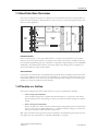
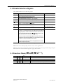
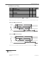
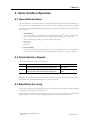
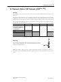
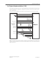
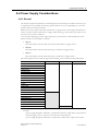
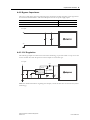
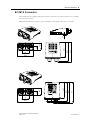
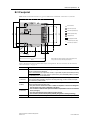
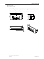
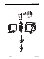
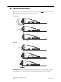
Hardware Design Guide
Anybus CompactCom 30
®
Doc. Id. HMSI-168-31
Doc. Rev. 2.24
Twincomm
de Olieslager 44
5506 EV Veldhoven
the Netherlands
T +31-(0)40-2301.924
F +31-(0)40-2301.923
E [email protected]
www.twincomm.nl
Connecting DevicesTM
HALMSTAD • CHICAGO • KARLSRUHE • TOKYO • BEIJING • MILANO • MULHOUSE • COVENTRY • PUNE • COPENHAGEN
HMS Industrial Networks
Mailing address: Box 4126, 300 04 Halmstad, Sweden
Visiting address: Stationsgatan 37, Halmstad, Sweden
E-mail: [email protected]
www.hms-networks.com
Important User Information
This document is intended to provide a good understanding of the mechanical and electric properties of the Anybus CompactCom platform. It does not cover any of the network specific features offered by the various incarnations of the product; this information is instead available as separate documents (Network Interface Appendix).
The reader of this document is expected to be familiar with hardware design and communication systems in general. For more information, documentation etc., please visit the HMS web site, ‘www.anybus.com’.
Liability
Every care has been taken in the preparation of this manual. Please inform HMS Industrial Networks AB of any
inaccuracies or omissions. The data and illustrations found in this document are not binding. We, HMS Industrial
Networks AB, reserve the right to modify our products in line with our policy of continuous product development.
The information in this document is subject to change without notice and should not be considered as a commitment by HMS Industrial Networks AB. HMS Industrial Networks AB assumes no responsibility for any errors that
may appear in this document.
There are many applications of this product. Those responsible for the use of this device must ensure that all the
necessary steps have been taken to verify that the applications meet all performance and safety requirements including any applicable laws, regulations, codes, and standards.
HMS Industrial Networks AB will under no circumstances assume liability or responsibility for any problems that
may arise as a result from the use of undocumented features, timing, or functional side effects found outside the
documented scope of this product. The effects caused by any direct or indirect use of such aspects of the product
are undefined, and may include e.g. compatibility issues and stability issues.
The examples and illustrations in this document are included solely for illustrative purposes. Because of the many
variables and requirements associated with any particular implementation, HMS Industrial Networks AB cannot
assume responsibility for actual use based on these examples and illustrations.
Intellectual Property Rights
HMS Industrial Networks AB has intellectual property rights relating to technology embodied in the product described in this document. These intellectual property rights may include patents and pending patent applications
in the US and other countries.
Trademark Acknowledgements
Anybus ® is a registered trademark of HMS Industrial Networks AB. All other trademarks are the property of their
respective holders.
Warning:
This is a class A product. In a domestic environment this product may cause radio interference in
which case the user may be required to take adequate measures.
ESD Note: This product contains ESD (Electrostatic Discharge) sensitive parts that may be damaged if ESD
control procedures are not followed. Static control precautions are required when handling the product. Failure to observe this may cause damage to the product.
Anybus CompactCom 30 Hardware Design Guide
Rev 2.24
Copyright© HMS Industrial Networks AB
Apr 2014 Doc Id HMSI-168-31
Table of Contents
Table of Contents
Preface
About This Document
Related Documents.................................................................................................................................. 5
Document History ................................................................................................................................... 5
Conventions & Terminology.................................................................................................................. 6
Support ...................................................................................................................................................... 6
Chapter 1
Introduction
General Description................................................................................................................................. 7
Features...................................................................................................................................................... 7
Host Interface Overview......................................................................................................................... 8
Passive vs. Active ..................................................................................................................................... 8
M12 Connector......................................................................................................................................... 9
Chapter 2
Host Connector
Host Interface Signals............................................................................................................................ 10
Signal Descriptions................................................................................................................................. 12
OM[0...2] (Operating Mode) ........................................................................................................ 12
MI[0...1] (Module Identification)................................................................................................... 12
RESET (Reset Input)................................................................................................................... 13
MD[0...1] (Module Detection) ...................................................................................................... 14
Parallel Interface ............................................................................................................................ 14
Serial Interface ............................................................................................................................... 14
Safety Serial Interface (PROFINET 2-port only).......................................................................... 14
Network Status LED Outputs ..................................................................................................... 15
General Purpose I/O..................................................................................................................... 15
Chapter 3
Parallel Interface Operation
General Information.............................................................................................................................. 16
Parallel Interface Signals........................................................................................................................ 17
Function Table (CE, R/W, OE, D[0...7]) .......................................................................................... 17
Timing Diagrams.................................................................................................................................... 18
Read Access Timing....................................................................................................................... 18
Write Access Timing...................................................................................................................... 19
Network Identification .......................................................................................................................... 20
Chapter 4
Serial Interface Operation
General Description............................................................................................................................... 21
Serial Interface Signals........................................................................................................................... 21
Baud Rate Accuracy ............................................................................................................................... 21
Chapter 5
General Purpose I/O
General..................................................................................................................................................... 22
Functional Description.......................................................................................................................... 22
Appendix A Implementation Guidelines
Module Compatibility ............................................................................................................................ 23
Additional Address Lines (A[11...13])................................................................................................. 23
Network Status LED Outputs (LED[1A...2B]) ................................................................................ 24
Typical Implementation (3.3V) ............................................................................................................ 25
Interfacing to 5V Logic ......................................................................................................................... 26
Power Supply Considerations............................................................................................................... 27
General.......................................................................................................................................... 27
Bypass Capacitance ........................................................................................................................ 28
3.3V Regulation ........................................................................................................................... 28
Appendix B Mechanical Specification
Overview ................................................................................................................................................. 29
M12 Connector....................................................................................................................................... 30
Footprint.................................................................................................................................................. 31
Housing Preparations ............................................................................................................................ 32
Slot Cover................................................................................................................................................ 33
Host Connector...................................................................................................................................... 34
Host Connector Considerations....................................................................................................... 36
Host Connector Pin Numbering..................................................................................................... 36
Fastening Mechanics.............................................................................................................................. 37
Appendix C Technical Specification
Environmental ........................................................................................................................................ 38
Shock and Vibration .............................................................................................................................. 38
Electrical Characteristics ....................................................................................................................... 39
Regulatory Compliance ......................................................................................................................... 40
Preface
P. About This Document
For more information, documentation etc., please visit the HMS website, ‘www.anybus.com’.
P.1 Related Documents
Document
Anybus CompactCom Software Design Guide
Anybus CompactCom Driver User Manual
Anybus CompactCom 30 Network Appendix (separate document for each supported fieldbus system)
Anybus CompactCom Brick and without Housing Design Guide
Low-Cost, Low-Power Level Shifting in Mixed-Voltage (5V, 3.3V) Systems (SCBA002A)
LT1767 Data sheet
EN 60950
EN 61000
EN 55011
Author
HMS
HMS
HMS
HMS
Texas Instruments
Linear Technology
European Union
European Union
European Union
P.2 Document History
Summary of Recent Changes (2.23... 2.24)
Change
Added service mode in chapter 2.2.1
Updated support information
Page(s)
12
6
Revision List
Revision
1.00 - 1.25
2.00
2.10
2.11
2.12
2.20
2.21
2.22
2.23
2.24
Date
Author
2010-05-31
2012-02-29
2012-05-25
2012-05-31
2012-09-13
2013-04-02
2013-05-13
2014-01-28
2014-04-01
KeL
KeL
KeL
KeL
KeL
KeL
KaD
KeL
KaD
Chapter(s) Description
See earlier revisions
All
Major update
2, 3, A
Updates
B
Minor update
B
Minor correction
1, 2, B
New connector type, minor corrections
2, 5
Minor update
P, B
Minor update
1, 2
Added info on functional safety, minor corrections
2
Minor updates
Anybus CompactCom 30 Hardware Design Guide
Doc.Rev. 2.24
Doc.Id. HMSI-168-31
About This Document 6
P.3 Conventions & Terminology
The following conventions are used throughout this manual:
•
Numbered lists provide sequential steps
•
Bulleted lists provide information, not procedural steps
•
The term ‘Anybus’ or ‘module’ refers to the Anybus CompactCom.
•
The terms ‘host’ or ‘host application’ refers to the device that hosts the Anybus module.
•
Hexadecimal values are written in the format NNNNh or 0xNNNN, where NNNN is the hexadecimal value.
•
A byte always consists of 8 bits.
•
All measurements in this document have a tolerance of ±0.20mm unless otherwise stated.
•
Outputs are TTL compliant unless otherwise stated.
•
Signals which are ‘pulled to NN’ are connected to NN via a resistor.
•
Signals which are ‘tied to NN’ are directly connected to NN.
P.4 Support
For general contact information and support, please refer to the contact and support pages at
www.anybus.com.
Anybus CompactCom 30 Hardware Design Guide
Doc.Rev. 2.24
Doc.Id. HMSI-168-31
Chapter 1
1. Introduction
1.1 General Description
The Anybus CompactCom network communication module is a high performance, low cost communication solution for industrial field devices. All Anybus CompactCom implementations share the same
footprint and electrical interface, allowing the host application to support all major networking systems
using the same hardware platform.
Two different host interface options are provided, serial and parallel, allowing easy integration into almost any platform. The parallel interface is based on a dual port memory architecture, where the host
application and the Anybus module exchange data by means of shared memory. This allows for very
efficient data exchange, and generally produces very little overhead for the host application. The serial
interface is a common asynchronous serial interface which can operate at baud rates from 19.2 kbps 625 kbps.
A unique mechanical concept allows the module to be implemented as an end-user option (plug-in), or
embedded into the host product at the manufacturing stage. The plug-in concept allows the vendor to
assemble and ship their product without the Anybus CompactCom module fitted. The end user can then
at a later stage decide whether to install an Anybus module or not.
Typical applications are Frequency Inverters, PLC's, HMI's, Visualization Devices, Instruments, Scales,
Robotics and Intelligent measuring devices.
1.2 Features
•
Integrated protocol stack handling (Where applicable)
•
Galvanically isolated network interface (Where applicable)
•
On-board network status indications according to each network standard (Where applicable)
•
On-board network connectors according to each network standard
•
Compact size (52 x 50mm, 2” x 1.97”)
•
Firmware upgradable (FLASH technology)
•
3.3 V design
•
Low power consumption
•
Parallel & serial interface modes
•
Pre-compliance tested for network conformance (Where applicable)1
•
Pre-compliance tested for CE & UL
•
Version with M12 connector available for PROFINET (2-port), EtherNet/IP (2-port), ModbusTCP (2-port), PROFIBUS DP-V1, EtherCAT, and DeviceNet.
•
Support for functional safety communication (PROFINET 2-port)
1. All Anybus CompactCom versions will be pre-certified for network conformance. While this is done to
ensure that the final product can be certified, it does not necessarily mean that the final product does not
require re-certification. Contact HMS for further information.
Anybus CompactCom 30 Hardware Design Guide
Doc.Rev. 2.24
Doc.Id. HMSI-168-31
Introduction 8
1.3 Host Interface Overview
The Anybus CompactCom features two different host communication interfaces. The figure below illustrates the basic properties of these interfaces as well as various I/O and control signals, and how they
relate to the host application.
Parallel Interface
IRQ
Host
CPU
Tx
Rx
Serial Interface
GOP[0...1]
GIP[0...1]
I/O
Anybus
CPU
Network
CE
OE
R/W
Physical Interface
RAM
Communications Controller
Flash
A0 ... A13
D0 ... D7
RESET
OM[0...2]
MI[0...1]
MD[0...1]
Parallel Interface
From an external point of view, the parallel interface is a common 8 bit parallel slave port interface,
which can easily be incorporated into any microprocessor based system that has an address/data type
bus. Generally, implementing this type of interface is comparable to implementing an 8 bit wide SRAM.
Additionally, the parallel interface features an interrupt request line, allowing the host application to
service the module only when actually needed.
Serial Interface
Compared to the serial interface, the parallel interface generally offers much higher performance. However, in some applications this solution may be impractical, e.g. when the host CPU doesn’t have an external address/data bus etc. In such cases, the serial interface provides a simple way of interfacing the
module via a common asynchronous serial interface.
1.4 Passive vs. Active
The Anybus CompactCom product family features two types of communication modules:
•
Active CompactCom Modules
Active modules integrates the complete network functionality (i.e. the protocol stack and the
physical interface) in the same package in order to provide network data exchange in a uniform
manner.
•
Passive CompactCom Modules
Passive modules uses a subset of the host interface signals, and generally operates on the physical
level of a serial signal (i.e. RS-232, RS-485 etc.), or enables serial data exchange on another medium/protocol such as USB or Ethernet (serial server).
Both types of modules can be supported in the host application by implementing the proper host interface signals. For more information, see “Module Compatibility” on page 23.
Anybus CompactCom 30 Hardware Design Guide
Doc.Rev. 2.24
Doc.Id. HMSI-168-31
Introduction 9
1.5 M12 Connector
A number of the Anybus CompactCom 30 modules are available with an M12 connector instead of the
usual network connector. This applies for the EtherNet/IP (2-port), PROFINET (2-port), PROFIBUS
DP-V1, Modbus-TCP (2-port), and DeviceNet modules.
The M12 connector gives the opportunity to raise the IP rating of a product up to IP67. However, the
standard Anybus CompactCom housing does not qualify for IP ratings above IP20. If a higher rating is
needed, careful design of housings and/or module fronts is necessary. It is then recommended to use
the Anybus CompactCom 30 module without housing, and design a new housing/front that fulfills the
requirements for IP67.
Anybus CompactCom 30 Hardware Design Guide
Doc.Rev. 2.24
Doc.Id. HMSI-168-31
Chapter 2
2. Host Connector
2.1 Host Interface Signals
The Anybus CompactCom host interface
uses a 50 pin CompactFlash™ style connector.
MD1
A1
A3
A5
A7
A9
A11
A13
D6
D4
D2
D0
VDD
VSS
OM1
CE
IRQ
RESET
GOP0
GIP0
LED2B
LED1B
Tx
MI1
VSS
Important Note:
The host interface is not pin compatible
with the CompactFlash™ standard, nor is
it hot-swap capable. Failure to observe
this may damage to the host product and/
or the Anybus CompactCom module.
1
26
VSS
A0
A2
A4
A6
A8
A10
A12
D7
D5
D3
D1
VDD
VSS
OM0
OM2
R/W
OE
GOP1
GIP1
LED2A
LED1A
Rx
MI0
MD0
25
50
Also note that the passive CompactCom modules use a limited number of the host interface signals.
Each signal presented in the tables below is described in detail later in this document.
Active modules
Position
36, 11, 35
Signal
OM[0...2]
Type
I
Function
Operating Mode
Page
12
27, 2
MI[0...1]
O
Module Identification
12
8
RESET
I
Reset Input, active low
13
26, 25
MD[0...1]
O
Module Detection
14
14, 39, 15, 40, 16, 41, 17, 42
D[0...7]
BI
Parallel Interface
17
Note: When the serial interface is used by the Anybus
CompactCom 30 module, signals A12 and A13 can be
used for functional safety communication (Anybus
CompactCom 30 PROFINET 2-Port module only). For
more information, see “Safety Serial Interface (PROFINET 2-port only)” on page 14.
49, 24, 48, 23, 47, 22, 46, 21, A[0...13]
45, 20, 44, 19, 43, 18
10
CE
33
OE
I
34
R/W
I
9
IRQ
Rx
Tx
LED2A
LED1A
LED2B
LED1B
O
28
3
30
29
5
4
6, 31
GIP[0...1]
7, 32
13, 38
1, 12, 37, 50
I
O
BI
P
GOP[0...1]
VDD
VSS
= Input, CMOS (3.3V)
= Output, CMOS (3.3V)
= Bidirectional, Tristate
= Power supply inputs
I
I
I
O
O
O
O
O
I
Serial Interface
21
Network Status LED Outputs
15
General Purpose I/O
22
Power Supply
Ground
27
O
PWR
PWR
Note: None of the host interface signals are 5V tolerant.
Note 1: For mechanical properties, measurements etc. see “Mechanical Specification” on page 29.
Note 2: For electrical characteristics, see “Electrical Characteristics” on page 39
Anybus CompactCom 30 Hardware Design Guide
Doc.Rev. 2.24
Doc.Id. HMSI-168-31
Host Connector 11
Passive modules
Position
27, 2
MI[0...1]
Signal
Type
O
Function
Module Identification
Page
12
8
RESET
I
Reset Input, active low
13
26, 25
MD[0...1]
O
Module Detection
14
14, 39, 15, 40, 16, 41, 17, 42 D[0...7]
BI
Parallel Interface
17
10a
CE
I
34a
R/W
I
33a
28
3
30
29
5
4
6
OE
Rx
Tx
LED2A
LED1A
LED2B
LED1B
I
Serial Interface
21
Network Status LED Outputs
15
General Purpose I/O
22
Power Supply
Ground
(not used)
27
GIP[0...1]
7
GOP[0...1]
13, 38
VDD
1, 12, 37, 50
VSS
9, 11, 18, 19, 20, 21, 22, 23, 24, 31, 32, 35, 36, 43, 44, 45,
46, 47, 48, 49
I
O
BI
P
NC
= Input, CMOS (3.3V)
= Output, CMOS (3.3V)
= Bidirectional, Tristate
= Power supply inputs
= Not connected
I
O
O
O
O
O
I
O
PWR
PWR
NC
Note: None of the host interface signals are 5V tolerant.
a. The type of a passive module can be identified from host interface signals D0-D7 (on the parallel interface) if CE
(10) and OE (33) are set to low and R/W (34) to high, see also “Network Identification” on page 20.
Note 1: For mechanical properties, measurements etc. see “Mechanical Specification” on page 29.
Note 2: For electrical characteristics, see “Electrical Characteristics” on page 39
Anybus CompactCom 30 Hardware Design Guide
Doc.Rev. 2.24
Doc.Id. HMSI-168-31
Host Connector 12
2.2 Signal Descriptions
2.2.1 OM[0...2] (Operating Mode)
On active modules, these inputs selects which interface that should be used to exchange data (parallel
or serial) and, if the serial interface option is used, the operating baud rate. The state of these signals is
sampled once during startup, i.e. any changes requires a reset in order to have effect.
Parallel interface State
Enabled
(disabled, see note 2)
Operating Mode
Serial interface State
(disabled, se note 2)
Enabled, baud rate: 19.2kbps
Enabled, baud rate: 57.6kbps
Enabled, baud rate: 115.2kbps
Enabled, baud rate: 625kbps
(reserved)
Service mode
OM2
LOW
LOW
LOW
LOW
HIGH
HIGH
HIGH
HIGH
Setting
OM1
LOW
LOW
HIGH
HIGH
LOW
LOW
HIGH
HIGH
OM0
LOW
HIGH
LOW
HIGH
LOW
HIGH
LOW
HIGH
LOW = VIL
HIGH = VIH
For more information regarding the parallel and serial interfaces, see “Parallel Interface Operation” on
page 16 and “Serial Interface Operation” on page 21.
Note 1: The state of these signals must be stable prior to releasing the RESET signal (see “RESET (Reset Input)” on page 13). Failure to observe this may result in faulty or unexpected behavior.
Note 2: These signals have no effect on passive modules; instead the communication settings are determined by other network specific factors. Furthermore, a subset of the parallel interface signals are used
for network identification purposes, see “Additional Address Lines (A[11...13])” on page 23.
2.2.2 MI[0...1] (Module Identification)
These signals indicate which type of module that is connected. It is recommended to check the state of
these signals before accessing the module.
State
MI0
LOW
HIGH
LOW
HIGH
MI1
LOW
LOW
HIGH
HIGH
Module Type
Anybus CompactCom (Active module)
Anybus CompactCom (Passive module)
(reserved)
LOW = VOL
HIGH = VOH
Anybus CompactCom 30 Hardware Design Guide
Doc.Rev. 2.24
Doc.Id. HMSI-168-31
Host Connector 13
2.2.3 RESET (Reset Input)
Active low master reset input. This signal should be connected to a host application controllable output
pin in order to be able to support network reset requests etc.
The module does not feature any internal reset regulation, which means that the host application is solely
responsible for resetting the module in case the supply voltage has gone outside the specified range (see
“Electrical Characteristics” on page 39). If this requirement is not fulfilled, a power brown-out (a drop
in voltage) may cause unwanted side-effects such as data loss in nonvolatile memory etc.
There is no schmitt trigger circuitry on this signal, which means that the module requires a fast RESET
rise time, preferably equal to the slew rate of typical logical circuits. Stable operation is not guaranteed
unless RESET slews from logic 0 (zero) to 1 at a minimum rate; i.e. a simple RC-circuit is not sufficient.
Note: Since some devices may be powered from the network, this signal must be pulled to VSS on the
host application side.
Reset (Powerup)
During startup, the reset signal must be held low as shown in the figure below.
Power
On
Power
Stable
3.3V
Power
t
0V
tA
tB
VIH
/RESET
VIL
Symbol Min.
tA
tB
t
Max. Definition
50 ms Power supply rise time (0.1 VCC to 0.9 VCC).
100 ms -
Safety margin.
Reset (Restart)
The reset pulse duration must be at least 100µs in order for the module to properly recognize a reset.
tC
VIH
RESET
t
VIL
Symbol Min.
Max.
100µs tC
Definition
Reset pulse width.
Anybus CompactCom 30 Hardware Design Guide
Doc.Rev. 2.24
Doc.Id. HMSI-168-31
Host Connector 14
2.2.4 MD[0...1] (Module Detection)
These signals are internally connected to VSS, and can be used by the host application to detect whether
a module is present or not.
State
MD0
HIGH
LOW
HIGH
LOW
MD1
HIGH
HIGH
LOW
LOW
Indication
Module not present
Module present
LOW = VOL
HIGH = VOH
Note: If unused, leave these signals unconnected.
2.2.5 Parallel Interface
For a description of the parallel interface signals, see “Parallel Interface Operation” on page 16.
2.2.6 Serial Interface
For a description of the serial interface signals, see “Serial Interface Operation” on page 21.
2.2.7 Safety Serial Interface (PROFINET 2-port only)
If the parallel interface is used for the host application, the serial interface can be used for functional
safety communication, using an add on safety module. If the host application uses the serial interface,
an extra serial channel, only for functional safety communication, will be used:
Position
43
18
Signal
ASM_Rx
ASM_Tx
Type
I
O
Function
Functional safety communication. If a Safety Module is
connected, these signals must not be tied to VDD.
Functional safety communication is only available for Anybus CompactCom 30 PROFINET 2-port.
For more information, see the Anybus CompactCom 30 PROFINET 2-port Network Appendix.
Anybus CompactCom 30 Hardware Design Guide
Doc.Rev. 2.24
Doc.Id. HMSI-168-31
Host Connector 15
2.2.8 Network Status LED Outputs
In some applications, the module may be mounted in a fashion that does not enable the user to see the
on-board network indication LEDs. The LED[1A....2B] outputs are directly connected to the internal
CPU and the on-board LEDs, and can be used to relay the network status indications to elsewhere on
the host application.
Note that these outputs are unbuffered and thus not capable of driving LEDs directly.
Led # Corresponding Signals
1
LED1A
Front View
Fieldbus connector
1
2
LED1B
2
M12 connectors
LED2A
1
2
LED2B
Note 1: If unused, leave these signals unconnected.
Note 2: The placement and the numbering of the LEDs in this picture are only given as an example.
Please refer to the network interface appendices for each specific module.
See also “Network Status LED Outputs (LED[1A...2B])” on page 24.
2.2.9 General Purpose I/O
See “General Purpose I/O” on page 22.
Anybus CompactCom 30 Hardware Design Guide
Doc.Rev. 2.24
Doc.Id. HMSI-168-31
Chapter 3
3. Parallel Interface Operation
3.1 General Information
Passive and active modules behave slightly differently concerning the parallel interface:
•
Active Modules
On active modules, the parallel interface is based on an asynchronous dual port memory architecture, allowing the Anybus module to be interfaced directly as a memory mapped peripheral.
For increased efficiency, an optional interrupt request signal (IRQ) allows the host application to
service the Anybus module only when necessary. Polled operation is also possible, albeit at the
cost of a slightly overhead.
On active modules, the parallel interface must be enabled using OM[0... 2].
See also...
- “OM[0...2] (Operating Mode)” on page 12)
•
Passive Modules
Passive module uses a subset of the parallel interface signals to provide means of network identification. Unlike active modules, it is not necessary to activate this functionality using OM[0... 2].
The serial interface remains enabled and is used as the main channel of communication.
See also...
- “Network Identification” on page 20
See also...
•
“Introduction” on page 7 (“Passive vs. Active” on page 8)
•
“Implementation Guidelines” on page 23(“Module Compatibility” on page 23)
IMPORTANT: The parallel interface does not support sequential or nonsequential burst access methods.
Anybus CompactCom 30 Hardware Design Guide
Doc.Rev. 2.24
Doc.Id. HMSI-168-31
Parallel Interface Operation 17
3.2 Parallel Interface Signals
The parallel interface uses the following signals:
Signal
Description
Mandatory address input signals.
Selects source/target location in shared memory.
Additional address input signals (optional)
(See “Additional Address Lines (A[11...13])” on page 23)
Notes
Tie to VSS when unused
D[0...7]
Bidirectional data bus. Target location is specified by A[0...13]
Tie to VSS when unused
CE
Bus chip enable; enables parallel access to the module when low.
Note: A[0...13] must be stable while CE is active.
Tie to VDD when unused
R/W
Bus read/write; enables input on D[0...7] when low.
Tie to VDD when unused
OE
Bus output enable; enables output on D[0...7] when low.
Tie to VDD when unused
IRQ
Active low Interrupt Request signal. Asserted by the Anybus module, and Leave unconnected if unused
de-asserted (i.e. acknowledged) by the host application by reading the Status Register (3FFFh). Please note that due to technical reasons, the module may acknowledge interrupts even if OE has not been asserted, if this
address (3FFFh) is present on the bus while CE is active.
A[0...10]
A[11...13]
Tie to VDD when unuseda
The use of this signal is optional albeit highly recommended. Even if the
host application lacks interrupt capabilities, it is recommended to connect
this signal to an input port to simplify software design.
This signal must be pulled to VDD on the host application side to prevent
spurious interrupts during startup.
a. Please note that if a Safety Module is connected, these signals must not be tied to VDD.
Note: There are no internal pullup resistors on any of the signals above.
Note: It is important to connect the serial interface signals correctly for proper functioning of the parallel interface. See “Serial Interface Signals” on page 21 for details.
3.3 Function Table (CE, R/W, OE, D[0...7])
CE
R/W
OE
HIGH
LOW
X
LOW
X
X
LOW
HIGH
LOW
LOW
HIGH
HIGH
X =Don’t care
D[0...7] State
High impedance
Data Input (Write)
Comment
Module not selected.
Data on D[0...7] is written to shared memory.
Data Output (Read) Data from shared memory is available on D[0...7]
High impedance
Module is selected, but D[0...7] is in a high impedance state.
LOW = VIL
HIGH = VIH
Anybus CompactCom 30 Hardware Design Guide
Doc.Rev. 2.24
Doc.Id. HMSI-168-31
Parallel Interface Operation 18
3.4 Timing Diagrams
Note: Timing depends on capacitive load. The figures in this section are valid for loads up to 25 pF.
Note: CE must be high at least 3 ns between two accesses. This is applicable in both Read and Write
Cycle.
3.4.1 Read Access Timing
Symbol
tAV
tAA
tACE
tAR
tAH
tLZ
tHZ
Parameter
Address Valid After Chip Enable
Address Access Time
Chip Enable Access Time
Min.
-
Max.
7
30
30
15
b
0
0
-
Output High-Z Timec
-
15
Read Access Timea
Address Hold Time
Output Low-Z Time
Unit
ns
a. Start of valid data depends on which timing becomes effective last; tAR, tACE or tAA
b. Timing depends on which signal is asserted last, OE or CE
c. Timing depends on which signal is de-asserted first, OE or CE
Read Access Timing1
Address
Address Valid
tAH
tACE
CE
tAR(a)
tAV
tHZ(c)
OE
tHZ(c)
tLZ(b)
D[0...7] (Out)
Data Valid
tLZ(b)
tAA
1. R/W = HIGH.
Anybus CompactCom 30 Hardware Design Guide
Doc.Rev. 2.24
Doc.Id. HMSI-168-31
Parallel Interface Operation 19
3.4.2 Write Access Timing
Symbol
tWC
tSW
tAW
tAS
Parameter
Write Cycle Time
Chip Enable to End-of-Write
Address Valid to End-of-Write
tWP
Write Pulse Widthb
Address Hold Time
Address Valid After Chip Enable
Data Valid to End-of-Write
Data Hold Time
Address Set-up Timea
tAH
tAV
tDW
tDH
Min.
30
25
25
0
Max.
-
25
-
0
15
0
7
-
Unit
ns
a. Timing depends on which enable signal (CE or R/W) is asserted last
b. A write occurs during the overlap (tSW or tWP) of CE = LOW and R/W = LOW
Note: Timing depends on capacitive load. The figures in this section are valid for loads up to 25 pF.
Write Cycle (R/W controlled timing)1
tWC
tAV
Address
tAH
tAW
CE
tAS(a)
tWP(b)
tAH
R/W
tDW
tDH
D[0...7] (In)
Write Cycle (CE controlled timing)2
tWC
Address
tAW
CE
tAS(a)
tSW(b)
tAH
R/W
tDW
[0...7]
D
tDH
(In)
Please note that once the address is stable it must not change for the duration of the low CE signal.
1. OE = HIGH
2. OE = Don’t care
Anybus CompactCom 30 Hardware Design Guide
Doc.Rev. 2.24
Doc.Id. HMSI-168-31
Parallel Interface Operation 20
3.5 Network Identification
As mentioned previously, the host application can detect the module type by examining the state of the
MI[0...1] signals. On passive modules, the network type can then be established by reading a byte in the
range 3800h... 38FFh.1 In case of active modules, the network type is retrieved by means of the host
interface protocol (consult the Anybus CompactCom Software Design Guide for further information).
In case the host application for some reason cannot use the MI[0...1] signals, it is still possible to retrieve
the module and network type as follows:
1. Release RESET signal
2. Wait at least 1.5 s2 (if only using passive modules, skip this step)
3. Read a byte in the range 3800h... 38FFh
The result obtained while reading from the range 3800h... 38FFh shall be interpreted as follows:
Value
00h
Module Type & Network
Active module (network type identified by means of the host communication protocol)
01h
Passive module, RS232
02h
Passive module, RS422
03h
Passive module, USB
04h
(reserved for future use)
05h
Passive module, Bluetooth
06h
(reserved for future use)
07h
(reserved for future use)
08h... 09h
(reserved for future use)
0Ah
Passive module, RS485
(0Bh... FFh)
(reserved for future use)
See also...
•
“Introduction” on page 7 (“Passive vs. Active” on page 8)
•
“General Information” on page 16
•
“Implementation Guidelines” on page 23 (“Module Compatibility” on page 23)
•
Anybus CompactCom Software Design Guide
1. The type of a passive module can also be identified from host interface signals D0-D7 (on the parallel
interface) if CE (10) and OE (33) are set to low and R/W (34) to high.
2. This time correlates to the start-up procedure (Initial Handshake) described in the Anybus CompactCom
Software Design Guide.
Anybus CompactCom 30 Hardware Design Guide
Doc.Rev. 2.24
Doc.Id. HMSI-168-31
Chapter 4
4. Serial Interface Operation
4.1 General Description
The serial interface is a common asynchronous serial interface, which can easily be interfaced directly to
a micro controller or UART (For connection examples etc., see “Interfacing to 5V Logic” on page 26).
The serial interface is handled differently depending on which type of module that is used (active or passive), see below.
•
Active Modules
On active modules, the serial interface is activated using the (OM[0...2]) inputs, which are also
used to select the operating baud rate (see “OM[0...2] (Operating Mode)” on page 12).
Other communication settings are fixed to the following values:
Data bits: 8
Parity: None
Stop bits: 1
•
Passive Modules
On passive modules, the serial interface is always active (regardless of the state of the OM[0...2]
inputs), and the communication settings are determined by other factors (network specific).
4.2 Serial Interface Signals
The serial interface option uses only two signals:
Signal
Tx
Description
TTL-compliant asynchronous serial transmit output.
This signal must be pulled to VDD on the host application side.
Rx
Asynchronous serial receivea.
This signal must be pulled to VDD on the host application side.
Notes
Leave this signal unconnected
when unused.
Tie this signal to VDD when
unused.
a. This input is not 5V tolerant
Note: It is important to connect the parallel interface signals correctly for proper functioning of the serial interface. See “Parallel Interface Signals” on page 17 for details.
4.3 Baud Rate Accuracy
As with most asynchronous communication devices, the actual baud rate used on the Anybus CompactCom may differ slightly from the ideal baud rate.
The baud rate error of the Anybus module is less than ±1.5%. For proper operation, it is recommended
that the baud rate accuracy in the host application lies within ±1.5% from the ideal value.
Anybus CompactCom 30 Hardware Design Guide
Doc.Rev. 2.24
Doc.Id. HMSI-168-31
Chapter 5
5. General Purpose I/O
5.1 General
The functionality of these signals is module type dependent. These signals have no dedicated function,
but it is still generally recommended to connect these signals to discreet inputs/outputs in the host application to be prepared for future functionality.
Signal Description
GIP0 General Input Port 0a
GIP1 General Input Port 1a
GOP0 General Output Port 0b
GOP1 General Output Port 1b
Notes
Active high general purpose input ports. Preferably, connect these inputs
to discreet outputs in the host application.
Note: These signals should be pulled to VSS on the host application.
Active low general purpose output ports. Preferably, connect these outputs to interrupt capable inputs on the host application.
Note: These signals should be pulled to VDD on the host application.
If unused, leave these signals unconnected.
a. Tie to VSS if unused.
b. If unused, leave these signals unconnected.
Please consult the network appendices for more information.
5.2 Functional Description
As mentioned previously, the function of these signals is different depending on module type. Please
check the Implementation Details section in the network appendix for each module for more information.
Active Modules
At the time of writing, some active modules use these signals. For example, the General Purpose IO
signals can, together with the LED[1A....2B] outputs, for some networks be used for extended LED
functionality. However it is strongly recommended to implement the signals in the host application in
order to be prepared for future functionality, whether or not they are used at the time being. Please consult the network appendices for more information.
Passive Modules
The following functionality has been defined for these signals when using passive modules:
Signal
GIP0
GIP1
GOP0
GOP1
Function
DE
(reserved)
CA
(reserved)
Notes
Data Enable; enables data transmission on half duplex networks such as RS-485.
Preferably, connect this input to a discreet output in the host application.
Communication Active; indicates if the connected network is ready for communication.
Preferably, connect this output to a discreet input in the host application.
Anybus CompactCom 30 Hardware Design Guide
Doc.Rev. 2.24
Doc.Id. HMSI-168-31
Appendix A
A. Implementation Guidelines
A.1 Module Compatibility
General
As mentioned previously, the Anybus CompactCom 30 product family holds two major types of communication modules called ‘Passive’ and ‘Active’. Both types can be supported in the host application
by implementing the proper host interface signals, see table below.
Compatibility Chart
Host Interface Implementation
General Purpose I/O
Serial Interface
Parallel Interface
Yes
Yes
Yes
No
Yes
No
Yes
Yes
Yes
Noa
Yes
No
No
Yes
Compatibility
Active Modules
Passive Modules
Yes
Yes
No
(Yes)
a
a. At the time of writing, the general purpose I/O signals (GIPx & GOPx) are unused on active modules. However,
since future products will utilize these signals for advanced fieldbus functions, it is generally recommended to
implement them anyway.
A.2 Additional Address Lines (A[11...13])
At the time of writing, address lines 11-13 are unused. Future products may however utilize these extra
address lines to accommodate a larger amount of high speed network I/O. To be able to take advantage
of this future functionality, it is recommended to implement as many of the address lines as possible.
Note: Unused address lines must be tied to VDD in order to maintain software compatibility and keep
the memory map intact, see table below. If a Safety Module is connected, A12 and A13 must not be tied
to VDD, though.
Available Address Lines
11
Recommendation
12
Implement A[0...11]. Tie A[12...13] to VDD
13
Implement A[0...12]. Tie A[13] to VDD
14
Implement A[0...13]
Implement A[0...10]. Tie A[11...13] to VDD
Anybus CompactCom 30 Hardware Design Guide
Doc.Rev. 2.24
Doc.Id. HMSI-168-31
Implementation Guidelines 24
A.3 Network Status LED Outputs (LED[1A...2B])
General
The LED[1A....2B] outputs can be used to relay the network status LEDs to elsewhere on the host application.
Note that it is the responsibility of the host application to ensure that each LED output is connected to
a LED of the correct color (on active modules, it is possible to retrieve this information from the Anybus
Object (01h); consult the general Anybus CompactCom Software Design Guide for more information).
An overview of the LED colors used are presented below. Most networks use the standard configuration, but there are a few exceptions.
Network
Standard configuration (Profibus
DP-V1 and DP-V0, DeviceNet,CANopen, Ethernet ModbusTCP, CC-Link etc.)
Modbus RTU
RS232
RS422
RS485
USB
LED1A
Green
LED1B
Red
Yellow
-
-
LED2A
Green
LED2B
Red
-
VDD
Buffering
The outputs are unbuffered, and cannot drive LEDs directly. In this example, a LED is connected to one of the LED outputs of the Anybus
module via an NPN transistor.
LEDnn
NPN
Note: The LED[1A....2B] outputs can, together with the General Purpose IO signals, for some networks be used for extended LED functionality. Please consult the network appendices for more information.
Anybus CompactCom 30 Hardware Design Guide
Doc.Rev. 2.24
Doc.Id. HMSI-168-31
Implementation Guidelines 25
A.4 Typical Implementation (3.3V)
The example in the figure below shows a typical implementation with both parallel- and serial communications, allowing the host application to support passive modules as well as active modules in either
serial or parallel mode.
Note that to increase readability, certain signals have intentionally been left out from this example.
A0 ... A13
A0 ... A13
D0 ... D7
D0 ... D7
CHIP SELECT
WRITE
READ
CE
R/W
OE
VDD
4.7k
4.7k
4.7k
Rx
Tx
Tx
Rx
IO PORT 1 (Interrupt Input)
IRQ
IO PORT 2 (Output)
RESET
VDD
4.7k
Host Application
CPU (3.3V)
4.7k
4.7k
IO PORT 3 (Input)
IO PORT 4 (Input)
IO PORT 5 (Output)
IO PORT 6 (Output)
GOP0
GOP1
GIP0
GIP1
VDD
4.7k
4.7k
4.7k
4.7k
IO PORT 7 (Input)
IO PORT 8 (Input)
IO PORT 9 (Input)
MI0
MI1
MD0
MD1
74LVC32
(3.3V)
VDD
OM0
OM1
OM2
4.7k
4.7k
4.7k
Note: As with many common microcontrollers, the direction of the IO PORT pins on the CPU in this
example is determined during power up; hence the pullup/pulldown resistors on the signals marked ‘IO
PORT (OUTPUT) n’.
Anybus CompactCom 30 Hardware Design Guide
Doc.Rev. 2.24
Doc.Id. HMSI-168-31
Implementation Guidelines 26
A.5 Interfacing to 5V Logic
The Anybus CompactCom is not 5V tolerant. This means that a level shifting circuit of some sort is required when interfacing the module in systems based on 5V logic. To better understand the issues involved when designing mixed voltage systems, it is recommended to read “Low-Cost, Low-Power Level
Shifting in Mixed-Voltage (5V, 3.3V) Systems” (Publication: SCBA002A) by Texas Instruments.
The example in the figure below uses four 74LVC245 bus transceivers powered with 3.3V to buffer the
signals towards Anybus module. The CHIPSELECT and READ signals from the host application CPU
are fed into a 74LVC32 logical ‘OR’ gate (also powered by 3.3V) of which the output is used to control
the direction of the bus transceiver that buffers the data bus.
VDD
A8
A9
A10
A11
A12
A13
VDD
VDD
4.7k
A0
A1
A2
A3
A4
A5
A6
A7
DIR
OE
A0
A1
A2
A3
A4
A5
A6
A7
DIR
OE
74LVC245 (3.3V)
A0
A1
A2
A3
A4
A5
A6
A7
B0
B1
B2
B3
B4
B5
B6
B7
A0
A1
A2
A3
A4
A5
A6
A7
74LVC245 (3.3V)
Note that to increase readability, certain signals have intentionally been left out from this example.
B0
B1
B2
B3
B4
B5
B6
B7
A8
A9
A10
A11
A12
A13
Rx
VDD
4.7k
Tx
Rx
A0
A1
A2
A3
A4
A5
A6
A7
DIR
OE
74LVC32
(3.3V)
CHIP SELECT
WRITE
READ
IO PORT 1 (Output)
IO PORT 2 (Output)
4.7k
4.7k
VDD
A0
A1
A2
A3
A4
A5
A6
A7
DIR
OE
74LVC245 (3.3V)
D0
D1
D2
D3
D4
D5
D6
D7
B0
B1
B2
B3
B4
B5
B6
B7
D0
D1
D2
D3
D4
D5
D6
D7
74LVC245 (3.3V)
Host Application
CPU (5V)
Tx
B0
B1
B2
B3
B4
B5
B6
B7
CE
R/W
OE
GIP0
GIP1
VDD
4.7k 4.7k
4.7k
GOP0
GOP1
IO PORT 3 (Input)
IO PORT 4 (Input)
IO PORT 5 (Interrupt Input)
IRQ
IO PORT 6 (Output)
4.7k
74LVC32
(3.3V)
RESET
Note: As with many common microcontrollers, the direction of the IO PORT pins on the CPU in this
example is determined during power up; hence the pullup/pulldown resistors on the signals marked ‘IO
PORT (OUTPUT) n’.
Anybus CompactCom 30 Hardware Design Guide
Doc.Rev. 2.24
Doc.Id. HMSI-168-31
Implementation Guidelines 27
A.6 Power Supply Considerations
A.6.1 General
The Anybus CompactCom platform in itself is designed to be extremely power efficient. The exact power requirements for a particular networking systems will however vary a lot depending on to the components used in the actual bus circuitry.
While most systems usually require less than 250 mA of supply current, certain high performance networks, or networks which require the use of legacy ASIC technology, will consume up to 500 mA, or in
rare cases even as much as 1000 mA.
As an aid when designing the power supply electronics, the networks have been divided into classes
based on their power consumption as follows.
•
Class A
This class includes systems which consume less than 250 mA of supply current.
•
Class B
This class includes systems which consume up to 500 mA of supply current.
•
Class C
This class includes systems which consume up to 1000 mA of supply current.
The following table lists the currently supported networking systems and their corresponding class.
Network
CANopen
DeviceNet
Modbus RTU
Profibus DP-V1
RS232 (Passive)
RS422/485 (Passive)
USB (Passive)
EtherNet/IP
Profibus DP-V0
CompoNet
Profinet
Modbus-TCP
BACnet MSTP
Bluetooth (Passive)
Sercos III
EtherCAT
Profinet 2-Port
Ethernet/IP 2-Port
CC-Link
BACnet/IP 2-Port
Modbus-TCP 2-Port
ControlNet
Class A
Yes
Class B
Yes
Class C
Yes
No
No
Examples:
A power supply designed to fulfil Class A requirements (250 mA), will be able to support all networks belonging to class A, but none of the networks in Class B and C.
A power supply designed to fulfil Class C requirements, will be able to support all networks.
Anybus CompactCom 30 Hardware Design Guide
Doc.Rev. 2.24
Doc.Id. HMSI-168-31
Implementation Guidelines 28
A.6.2 Bypass Capacitance
The power supply inputs must have adequate bypass capacitance for high-frequency noise suppression.
It is therefore recommended to add extra bulk capacitors near the power supply inputs:
Reference
C1
C2
Value (Ceramic)
22 uF / 6.3 V
100 nF / 16 V
Example:
VDD (3.3V)
VDD
C1
C2
GND
GND
A.6.3 3.3V Regulation
The following example uses the LT1767 from Linear Technology to provide a stable 3.3 V power source
for the module. Note that all capacitors in this example are of ceramic type.
Example:
BAV70
5V
VDD (3.3V)
BOOST
LT1767
Vin
Vsw
100nF
(16V)
10uH
Vc
1,5nF
(50V)
4k7
GND
100nF
(16V)
SYNC
SHDN
22uF
(6.3V)
FB
10uF
(6.3V)
SS14
GND
Note: For detailed information regarding this example, consult the data sheet for the LT1767 (Linear
Technology).
Anybus CompactCom 30 Hardware Design Guide
Doc.Rev. 2.24
Doc.Id. HMSI-168-31
Appendix B
B. Mechanical Specification
B.1 Overview
Note: The measurements below are given in millimeters and include a tolerance of ±0.20 mm.
A
C
B
C
18.9
18.1
8.4
A
New Grounding (VSS) Mechanics
B
Protective Earth (PE) Mechanics
C
Fastening Mechanics
0
1.3
3.4
0
33.7
39.6
49.2
50.7
51.8
1.7
R3
42.1
50.1
48
22.3
Anybus CompactCom 30 Hardware Design Guide
Doc.Rev. 2.24
Doc.Id. HMSI-168-31
Mechanical Specification 30
B.2 M12 Connector
The modules that are equipped with M12 connectors, either have two female connectors or one female
and one male connector.
64,7
21
62,7
50,7
22,3
12,7
3,4
Note: The measurements below are given in millimeters and include a tolerance of ±0.10 mm.
67
64,7
62,7
50,7
22,3
12,7
50,1
21
50,1
Anybus CompactCom 30 Hardware Design Guide
Doc.Rev. 2.24
Doc.Id. HMSI-168-31
Mechanical Specification 31
B.3 Footprint
Note 1: The measurements below are given in millimeters and include a tolerance of ±0.10 mm.
Reserved Area
A
33,0
6,5
44,0
4,4
7,3
33,0
9,8
VSS Plane (Coated)
A
VSS Plane (Conductive)
B
PE Area (Conductive)
Support Holes
Host Application PCB
Via (Connection to VSS)
CF Connector Outline
R1
,
5
6,9
51,0
B
9,4
7,0
5,5
3,0*
31,0
49,0
50,5
*Depending on Compact Flash connector. The plane/vias
may not be in contact with the pads for pins.
Note 2: Footprint for the recommended Anybus CompactCom 30 host connector can be found in
“Host Connector” on page 34.
Area
Description
Reserved Area To ensure isolation and mechanical compatibility, it is strongly advised that this area is kept completely
free from components and signal lines.
Under no circumstances may components, via holes, or signal lines, be placed on the PCB layer facing
the Anybus module. Failure to comply with this requirement may induce EMC/EMI problems, mechanical compatibility issues, or even short circuit.
PE Area
To achieve proper EMC behavior and to provide support for different cable shielding standards, this
(Conductive)
area must be tin plated (preferably using Hot Air Levelling technology) and have a stable, low impedance connection to protective earth.
VSS Plane
The exact shape of this area depends on the properties of the CompactFlash connector. It is however
(Coated)
important to follow these basic design rules:
• The plane must be continuous and have a stable, low impedance connection to VSS (preferably through at least 16 vias as illustrated in the figure)
•
The
connection to VSS should be placed beneath the CompactFlash connector as illustrated
VSS Plane
above (see figure)
(Conductive)
• The plane must follow the signal path through the connector
• The conductive part must be tin plated, preferably using Hot Air Levelling technology
Support Holes
These holes are used by the fastening mechanics to secure the module onto the host application.
Anybus CompactCom 30 Hardware Design Guide
Doc.Rev. 2.24
Doc.Id. HMSI-168-31
Mechanical Specification 32
B.4 Housing Preparations
Note: The measurements below are given in millimeters and include a tolerance of ±0.10 mm.
1.7
Front
R3
R2
1
1
48.6
20.8
22.9
1.1
0.8
6.5
33.6
R 0.5
50.8
Anybus CompactCom 30 Hardware Design Guide
Doc.Rev. 2.24
Doc.Id. HMSI-168-31
Mechanical Specification 33
B.5 Slot Cover
HMS can supply a “blind” slot-cover, which may be used to cover the Anybus CompactCom slot when
not in use, allowing the Anybus CompactCom module to be supplied as an end-user option instead of
being mounted during manufacturing.
Note: The measurements below are given in millimeters and include a tolerance of ±0.10 mm.
50.1
22.3
19.9 13.0
50.5
40.0
8.8
1.1
3.5
Anybus CompactCom 30 Hardware Design Guide
Doc.Rev. 2.24
Doc.Id. HMSI-168-31
Mechanical Specification 34
B.6 Host Connector
The Anybus CompactCom 30 is designed to use a compact flash connector as application connector. HMS offers a host connector, that is designed to simplify the
mounting and to meet the demands for a secure and stable connection of the Anybus CompactCom 30 modules.
The recommended PCB layout is presented in the figures
below.
Recommended PCB-layout
General tolerances ±0,05mm
40,2
38,7
31,115
0,45
2,3
4
D
46
Enable usage of
other connectors
(Second Source)
3,6
11,5
0,9
2,
3,5
18,5
1,7
15
8,1
3
0,635
Position hole
Position knob
50,87
DETAIL D
Please note that it is recommended to drill oval holes in the PCB, to enable usage of other connectors.
Warning: Always verify that the dimensions of another connector is compatible with this design.
Manufacturer
Part No.
Web
HMS Industrial Networks
SP1137
For more information visit the support pages for Anybus CompactCom 30 at www.anybus.com
Anybus CompactCom 30 Hardware Design Guide
Doc.Rev. 2.24
Doc.Id. HMSI-168-31
Mechanical Specification 35
The measurements of the connector are presented in the figure below.
Note: To ensure that you receive the correct measurements for the latest version of the connector,
please consult the support pages at www.anybus.com, where you will find all the latest available information for the connector.
Pin 25
Pin 50
Pin 1
Anybus CompactCom 30 Hardware Design Guide
Doc.Rev. 2.24
Doc.Id. HMSI-168-31
Mechanical Specification 36
B.6.1 Host Connector Considerations
When using other connectors, the following needs to be considered:
To prevent incorrect insertion and to ensure that the grounding mechanics work as intended, use connectors with guiding rails of sufficient length (preferably longer
than 19 mm), or provide an equivalent mechanical solution.
The distance of the connectors to the PCB has to conform to the picture below:
2.37
1.1
0
It is recommended to use connectors which can be screwed into the host application board, to minimize
mechanical strain on solder joints etc.
The following connectors have been verified for use with the Anybus CompactCom:
Manufacturer
Part No.
Web
Tyco
1734451-1
www.tycoelectronics.com
AllConnectors
101D-TAAB-R
www.allconnectors.de
Suyin
127531MB050XX04NA
www.suyin.com, www.suyin-europe.com, www.suyinusa.com
Harwin
M504-8815042
M504-88 25042
www.harwin.com
Note: The dimensions of the holes for the fixing pins of this connector is
1.8 mm, i.e. slightly larger than the dimensions given in the figure above.
B.6.2 Host Connector Pin Numbering
The surface mounted pins of the compact flash connector are numbered from left to right (see figure
below), corresponding to pin numbers 1, 26, 2, 27...... 25, 50 of the host interface connector, see “Host
Interface Signals” on page 10.
1
50
26
25
Bottom view of the host connector
Anybus CompactCom 30 Hardware Design Guide
Doc.Rev. 2.24
Doc.Id. HMSI-168-31
Mechanical Specification 37
B.7 Fastening Mechanics
Note 1: To support the fastening mechanism, the host application PCB must be 1.60 (±10%) mm thick.
Note 2: Recommended terminal tightening torque is 0.25 Nm.
Fastening
1
TORX 8
0.25Nm
2
3
Removal
1
TORX 8
2
3
IMPORTANT: When fastening the module into the end product, make sure that the Anybus module is properly
aligned into the CompactFlash socket prior to applying any force. Rough handling and/or excessive force in combination
with misalignment may cause mechanical damage to the Anybus CompactCom module and/or the end product.
Anybus CompactCom 30 Hardware Design Guide
Doc.Rev. 2.24
Doc.Id. HMSI-168-31
Appendix C
C. Technical Specification
Note: The properties specified in this chapter applies to all Anybus CompactCom modules unless otherwise stated. Any deviations from what is stated in this chapter is specified separately in each network
appendix.
C.1 Environmental
Operating temperature
Active modules:
Passive modules:
-40 to 70°C (-40 to 158°F)
-40 to 70°C (-40 to 158°F)
(Tests performed according to IEC 60068-2-1 and IEC 60068-2-2)
Storage temperature
Active modules:
Passive modules:
-40 to 85°C (-40 to 176°F)
-40 to 85°C (-40 to 176°F)
(Tests performed according to IEC 60068-2-1 and IEC 60068-2-2)
Humidity
Active modules:
Passive modules:
5 to 95% non-condensing
5 to 95% non-condensing
(Tests performed according to IEC 60068-2-30)
C.2 Shock and Vibration
•
Shock test, operating IEC 68-2-27 half-sine 30g, 11 ms, 3 positive and 3 negative shocks in each
of three mutually perpendicular directions
•
Shock test, operating IEC 68-2-27 half-sine 50g, 11 ms, 3 positive and 3 negative shocks in each
of three mutually perpendicular directions
•
Sinusoidal vibration, operating IEC 68-2-6 10-500 Hz, 0.35 mm, 5g, 1oct/min., 10 double-sweep
in each of three mutually perpendicular directions.
Anybus CompactCom 30 Hardware Design Guide
Doc.Rev. 2.24
Doc.Id. HMSI-168-31
Technical Specification 39
C.3 Electrical Characteristics
Operating Conditions
Symbol Parameter
Supply Voltage (DC)
VDD
Pin Types Conditions
PWR
-
Min.
3.15
Typ.
3.30
Max.
3.45
Unit
V
Ripple (AC)
-
-
± 100
mV
VSS
Ground reference
0.00
0.00
0.00
V
IIN
Current consumptiona
Class A
-
-
250
mA
Class B
-
-
500
mA
Class C
-
-
1000
mA
-
0.7 x VDD
-
VDD + 0.2
V
-0.2
-
0.2 x VDD
V
-
-4.0
-
4.0
mA
VIH
Input High Voltage
I, BI
VIL
Input Low Voltage
IOH
Current, Output High
IOL
Current, Output Low
VOH
Output High Voltage
IOH = -4mA
2.4
-
-
V
VOL
Output Low Voltage
IOL = 4mA
-
-
0.4
V
O, BI
a. See also A-27 “Power Supply Considerations”
I
= Input, CMOS (3.3V)
O
= Output, CMOS (3.3V)
BI = Bidirectional, Tristate
PWR = Power supply inputs
Isolation
Isolation distances for PCB between host, network, and PE (according to EN 60950-1; Pollution Degree
2; Material Group IIIb):
Isolation Barrier
Host to PE
Host to Network
Working Voltage/Transient Voltage
Creepage
Clearance
250V/2500V
250V/2500V
250V/2500V
250V/2500V
External
2.5mm
2.5mm
Distance
Internal
0.4mm
0.4mm
Protective Earth & Shielding
All Anybus CompactCom modules features a cable shield filter designed according to each network
standard. To be able to support this, the host application must have a conductive area connected to protective earth as described in B-29 “Mechanical Specification” (PE Connection Pad).
HMS cannot guarantee proper EMC behavior unless this requirement is fulfilled.
Anybus CompactCom 30 Hardware Design Guide
Doc.Rev. 2.24
Doc.Id. HMSI-168-31
Technical Specification 40
C.4 Regulatory Compliance
EMC Compliance (CE)
Since the Anybus CompactCom (ABCC) is considered a component for embedded applications, it cannot be CE-marked as an end product. However, the ABCC family is pre-compliance tested in a typical
installation providing that all modules conforms to the EMC directive in that installation.
Once the end product has successfully passed the EMC test using any of the ABCC modules, the precompliance test concept allows any other interface of the same type (see 1-8 “Passive vs. Active”) in the
ABCC family to be embedded in that product without further EMC tests.
To be compliant to the EMC directive 2004/108/EC, the pre-compliance testing has been conducted
according to the following standards:
•
Emission: EN61000-6-4
EN55011 Radiated emission
EN55011 Conducted emission
•
Immunity: EN61000-6-2
EN61000-4-2 Electrostatic discharge
EN61000-4-3 Radiated immunity
EN61000-4-4 Fast transients/burst
EN61000-4-5 Surge immunity
EN61000-4-6 Conducted immunity
Since all ABCC modules have been evaluated according to the EMC directive through the above standards, this serve as a base for our customers when certifying ABCC-based products.
UL/c-UL Compliance
The certification has been documented by UL in file E214107.
Anybus CompactCom 30 Hardware Design Guide
Doc.Rev. 2.24
Doc.Id. HMSI-168-31