1
S3FN429
32-bit CMOS Microcontrollers
Revision 1.20
May 2012
User's Manual
2012
Samsung Electronics Co., Ltd. All rights reserved.
Important Notice
Samsung Electronics Co. Ltd. ("Samsung") reserves the
right to make changes to the information in this publication
at any time without prior notice. All information provided is
for reference purpose only. Samsung assumes no
responsibility for possible errors or omissions, or for any
consequences resulting from the use of the information
contained herein.
This publication on its own does not convey any license,
either express or implied, relating to any Samsung and/or
third-party products, under the intellectual property rights of
Samsung and/or any third parties.
any information provided in this publication. Customer shall
indemnify and hold Samsung and its officers, employees,
subsidiaries, affiliates, and distributors harmless against all
claims, costs, damages, expenses, and reasonable attorney
fees arising out of, either directly or indirectly, any claim
(including but not limited to personal injury or death) that
may be associated with such unintended, unauthorized
and/or illegal use.
Customers are responsible for their own products and
applications. "Typical" parameters can and do vary in
different applications. All operating parameters, including
"Typicals" must be validated for each customer application
by the customer's technical experts.
WARNING No part of this publication may be reproduced,
stored in a retrieval system, or transmitted in any form or by
any means, electric or mechanical, by photocopying,
recording, or otherwise, without the prior written consent of
Samsung. This publication is intended for use by designated
recipients only. This publication contains confidential
information (including trade secrets) of Samsung protected
by Competition Law, Trade Secrets Protection Act and other
related laws, and therefore may not be, in part or in whole,
directly or indirectly publicized, distributed, photocopied or
used (including in a posting on the Internet where
unspecified access is possible) by any unauthorized third
party. Samsung reserves its right to take any and all
measures both in equity and law available to it and claim full
damages against any party that misappropriates Samsung's
trade secrets and/or confidential information.
Samsung products are not designed, intended, or authorized
for use in applications intended to support or sustain life, or
for any other application in which the failure of the Samsung
product could reasonably be expected to create a situation
where personal injury or death may occur. Customers
acknowledge and agree that they are solely responsible to
meet all other legal and regulatory requirements regarding
their applications using Samsung products notwithstanding
警 告 本文件仅向经韩国三星电子株式会社授权的人员提供,
其内容含有商业秘密保护相关法规规定并受其保护的三星电
子株式会社商业秘密,任何直接或间接非法向第三人披露、
传播、复制或允许第三人使用该文件全部或部分内容的行为
(包括在互联网等公开媒介刊登该商业秘密而可能导致不特
定第三人获取相关信息的行为)皆为法律严格禁止。此等违
法行为一经发现,三星电子株式会社有权根据相关法规对其
采取法律措施,包括但不限于提出损害赔偿请求。
Samsung makes no warranty, representation, or guarantee
regarding the suitability of its products for any particular
purpose, nor does Samsung assume any liability arising out
of the application or use of any product or circuit and
specifically disclaims any and all liability, including without
limitation any consequential or incidental damages.
Copyright 2012 Samsung Electronics Co., Ltd.
Samsung Electronics Co., Ltd.
San #24 Nongseo-Dong, Giheung-Gu
Yongin-City, Gyeonggi-Do, Korea 446-711
Contact Us: [email protected]
TEL:
(82)-(31)-209-4956
FAX:
(82)-(31)-8000-2005
Home Page: http://www.samsungsemi.com
Trademarks
All brand names, trademarks and registered trademarks belong to their respective owners.
Exynos, Exynos4210, FlexOneNAND, and OneNAND are trademarks of Samsung Electronics.
ARM, Jazelle, TrustZone, and Thumb are registered trademarks of ARM Limited. Cortex, ETM, ETB,
Coresight, ISA, and Neon are trademarks of ARM Limited.
Java is a trademark of Sun Microsystems, Inc.
SD is a registered trademark of Toshiba Corporation.
MMC and eMMC are trademarks of MultiMediaCard Association.
JTAG is a registered trademark of JTAG Technologies, Inc.
Synopsys is a registered trademark of Synopsys, Inc.
I2S is a trademark of Phillips Electronics.
I2C is a trademark of Phillips Semiconductor Corp.
MIPI and Slimbus are registered trademarks of the Mobile Industry Processor Interface (MIPI) Alliance.
All other trademarks used in this publication are the property of their respective owners.
Chip Handling Guide
Precaution against Electrostatic Discharge
When using semiconductor devices, ensure that the environment is protected against static electricity:
1. Wear antistatic clothes and use earth band.
2. All objects that are in direct contact with devices must be made up of materials that do not produce static
electricity.
3. Ensure that the equipment and work table are earthed.
4. Use ionizer to remove electron charge.
Contamination
Do not use semiconductor products in an environment exposed to dust or dirt adhesion.
Temperature/Humidity
Semiconductor devices are sensitive to:
Environment
Temperature
Humidity
High temperature or humidity deteriorates the characteristics of semiconductor devices. Therefore, do not store or
use semiconductor devices in such conditions.
Mechanical Shock
Do not to apply excessive mechanical shock or force on semiconductor devices.
Chemical
Do not expose semiconductor devices to chemicals because exposure to chemicals leads to reactions that
deteriorate the characteristics of the devices.
Light Protection
In non- Epoxy Molding Compound (EMC) package, do not expose semiconductor IC to bright light. Exposure to
bright light causes malfunctioning of the devices. However, a few special products that utilize light or with security
functions are exempted from this guide.
Radioactive, Cosmic and X-ray
Radioactive substances, cosmic ray, or X-ray may influence semiconductor devices. These substances or rays
may cause a soft error during a device operation. Therefore, ensure to shield the semiconductor devices under
environment that may be exposed to radioactive substances, cosmic ray, or X-ray.
EMS (Electromagnetic Susceptibility)
Strong electromagnetic wave or magnetic field may affect the characteristic of semiconductor devices during the
operation under insufficient PCB circuit design for Electromagnetic Susceptibility (EMS).
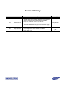
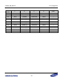
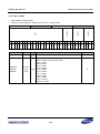
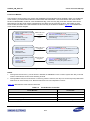
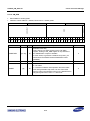
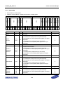
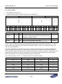
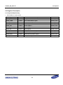
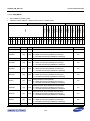
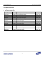
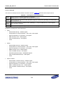
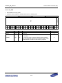
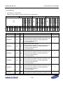
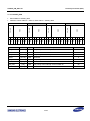
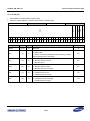
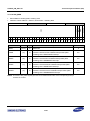
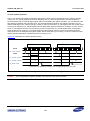
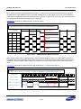
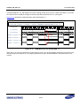
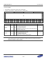
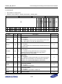
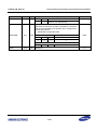
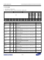
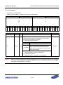
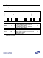
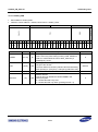
Revision History
Revision No.
1.00
Date
Jan. 17, 2012
Description
Promoted from preliminary to V1.0 and released
Author(s)
YH Jin
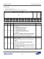
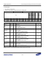
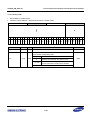
Added guide notes (caution) related to the pin (XIN and
XOUT) connection for unused external oscillator.
1.10
Feb. 22, 2012
Page 2-7, 5-8, 5-21, 5-41, 5-59, and 19-7
Corrected the errata.
MCU solution
part
The offset address of PPD_SCTVHR register in page
7-37 was fixed from 0x006C to 0x005C.
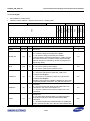
Added guide notes related to the pin (OPAMP output
1.20
May. 16, 2012
pin) configuration when OPAMP is enabled.
Page 12-5, 13-8
MCU solution
part
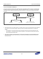
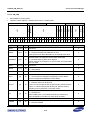
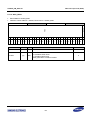
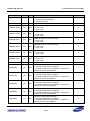
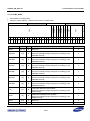
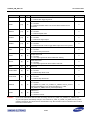
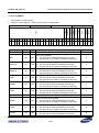
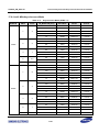
Table of Contents
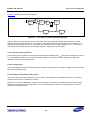
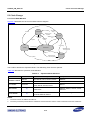
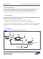
1 PRODUCT OVERVIEW .................................................................................1-1
1.1 Introduction .............................................................................................................................................. 1-1
1.2 Features ................................................................................................................................................... 1-2
1.3 Block Diagram .......................................................................................................................................... 1-9
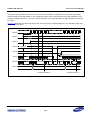
2 PIN CONFIGURATION ..................................................................................2-1
2.1 Overview .................................................................................................................................................. 2-1
2.2 Pin Map .................................................................................................................................................... 2-2
2.3 Pin Assignment ........................................................................................................................................ 2-3
2.4 Mirror Pins ................................................................................................................................................ 2-5
2.5 Pin Description ......................................................................................................................................... 2-6
2.5.1 Power Pins ........................................................................................................................................ 2-6
2.5.2 System Pins ...................................................................................................................................... 2-7
2.5.3 Function Pins .................................................................................................................................... 2-9
2.5.4 Debug Interface Pins ...................................................................................................................... 2-10
2.5.5 Flash Serial Program Pins .............................................................................................................. 2-10
2.6 Pin Circuit Type ...................................................................................................................................... 2-11
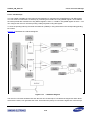
2.6.1 Block Diagram ................................................................................................................................ 2-11
3 SYSTEM MEMORY MANAGEMENT.............................................................3-1
3.1 Overview .................................................................................................................................................. 3-1
3.2 Default Memory Map ................................................................................................................................ 3-1
3.3 Special Function Register Map ................................................................................................................ 3-2
3.3.1 Core Special Function Register Map ................................................................................................ 3-2
3.3.2 Peripheral Special Function Register Map ....................................................................................... 3-3
4 ANALOG TO DIGITAL CONVERTER (ADC) ................................................4-1
4.1 Overview .................................................................................................................................................. 4-1
4.1.1 Features ............................................................................................................................................ 4-1
4.1.2 Pin Description.................................................................................................................................. 4-1
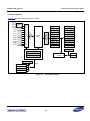
4.1.3 Block Diagram .................................................................................................................................. 4-2
4.1.4 Input and Output ............................................................................................................................... 4-3
4.1.5 Clock Frequency and Conversion Time ........................................................................................... 4-4
4.1.6 Conversion Mode.............................................................................................................................. 4-5
4.1.7 Conversion Start Trigger .................................................................................................................. 4-9
4.1.8 Conversion Data ............................................................................................................................. 4-10
4.1.9 Interrupt and Flag ........................................................................................................................... 4-10
4.1.10 Calibration ..................................................................................................................................... 4-11
4.1.11 Operation Sequence ..................................................................................................................... 4-14
4.2 Register Description ............................................................................................................................... 4-16
4.2.1 Register Map Summary .................................................................................................................. 4-16
5 CLOCK AND POWER MANAGER ................................................................5-1
5.1 Overview .................................................................................................................................................. 5-1
5.1.1 Features ............................................................................................................................................ 5-2
5.1.2 Block Diagram .................................................................................................................................. 5-4
5.2 Clocks ...................................................................................................................................................... 5-5
5.2.1 SYSCLK ............................................................................................................................................ 5-5
5.2.2 IMCLK ............................................................................................................................................... 5-7
5.2.3 EMCLK ............................................................................................................................................. 5-7
5.2.4 PLL ................................................................................................................................................... 5-8
5.2.5 Clock Monitor .................................................................................................................................. 5-11
5.2.6 Clock Out ........................................................................................................................................ 5-13
5.3 Clock Change......................................................................................................................................... 5-14
5.3.1 Clock State Machine ....................................................................................................................... 5-14
5.3.2 SYSCLK Change ............................................................................................................................ 5-16
5.3.3 WDTCLK Source Change .............................................................................................................. 5-16
5.4 Power Management ............................................................................................................................... 5-17
5.4.1 Operation Modes ............................................................................................................................ 5-17
5.4.2 Low Power Modes and Wake-Up ................................................................................................... 5-18
5.5 External Events (External Interrupts and Wake-up Event) .................................................................... 5-24
5.5.1 Operating Mode .............................................................................................................................. 5-24
5.5.2 Idle Modes ...................................................................................................................................... 5-25
5.5.3 Stop Modes ..................................................................................................................................... 5-25
5.6 Reset Management ................................................................................................................................ 5-26
5.6.1 nRESET Pin Reset (NRST) ............................................................................................................ 5-27
5.6.2 Power-On Reset (PORST) ............................................................................................................. 5-27
5.6.3 LVD Reset (LVDRST) ..................................................................................................................... 5-27
5.6.4 External Main Clock Monitor Reset (EMCMRST) .......................................................................... 5-29
5.6.5 Watchdog Timer Reset (WDTRST) ................................................................................................ 5-29
5.6.6 Software Reset (SWRST) ............................................................................................................... 5-29
5.6.7 CPU Request Reset (SYSRST) ..................................................................................................... 5-29
5.7 Basic Timer ............................................................................................................................................ 5-30
5.8 Fast Wake-up ......................................................................................................................................... 5-32
5.9 Register Description ............................................................................................................................... 5-34
5.9.1 Register Map Summary .................................................................................................................. 5-34
5.10 Guide-Clock Initialization ..................................................................................................................... 5-76
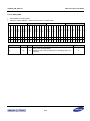
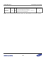
6 COMPARATOR .............................................................................................6-1
6.1 Overview .................................................................................................................................................. 6-1
6.1.1 Features ............................................................................................................................................ 6-1
6.1.2 Pin Description.................................................................................................................................. 6-1
6.2 Functional Description ............................................................................................................................. 6-2
6.2.1 Block Diagram .................................................................................................................................. 6-3
6.2.2 Comparator Input .............................................................................................................................. 6-4
6.2.3 Comparator Output ........................................................................................................................... 6-4
6.2.4 IMC Output-Off Control ..................................................................................................................... 6-4
6.2.5 Interrupt ............................................................................................................................................ 6-4
6.3 Register Description ................................................................................................................................. 6-5
6.3.1 Register Map Summary .................................................................................................................... 6-5
7 PULSE POSITION DECODER ......................................................................7-1
7.1 Overview .................................................................................................................................................. 7-1
7.1.1 Features ............................................................................................................................................ 7-1
7.1.2 Pin Description.................................................................................................................................. 7-1
7.2 Functional Description ............................................................................................................................. 7-2
7.2.1 Block Diagram .................................................................................................................................. 7-2
7.2.2 Operating Mode ................................................................................................................................ 7-3
7.3 Register Description ................................................................................................................................. 7-6
7.3.1 Register Map Summary .................................................................................................................... 7-6
8 GENERAL PURPOSE I/O (GPIO) .................................................................8-1
8.1 Overview .................................................................................................................................................. 8-1
8.1.1 Features ............................................................................................................................................ 8-1
8.1.2 Pin Description.................................................................................................................................. 8-1
8.2 Functional Description ............................................................................................................................. 8-2
8.2.1 GPIO Configuration .......................................................................................................................... 8-2
8.2.2 Input Configuration ........................................................................................................................... 8-2
8.2.3 Output Configuration ........................................................................................................................ 8-3
8.2.4 Operation Mode ................................................................................................................................ 8-3
8.2.5 Interrupt ............................................................................................................................................ 8-4
8.3 Register Description ................................................................................................................................. 8-5
8.3.1 Register Map Summary .................................................................................................................... 8-5
9 INTERNAL FLASH CONTROLLER (IFC) .....................................................9-1
9.1 Overview .................................................................................................................................................. 9-1
9.1.1 Features ............................................................................................................................................ 9-1
9.2 Functional Description ............................................................................................................................. 9-2
9.2.1 Organization ..................................................................................................................................... 9-3
9.2.2 Smart Option ..................................................................................................................................... 9-6
9.2.3 Modes ............................................................................................................................................. 9-10
9.2.4 Flow Chart ...................................................................................................................................... 9-16
9.2.5 Error ................................................................................................................................................ 9-22
9.3 Register Description ............................................................................................................................... 9-26
9.3.1 Register Map Summary .................................................................................................................. 9-26
10 INVERTER MOTOR CONTROLLER (IMC) ...............................................10-1
10.1 Overview .............................................................................................................................................. 10-1
10.1.1 Features ........................................................................................................................................ 10-1
10.1.2 Pin Description.............................................................................................................................. 10-1
10.2 Functional Description ......................................................................................................................... 10-2
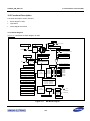
10.2.1 Block Diagram .............................................................................................................................. 10-2
10.2.2 Operation ...................................................................................................................................... 10-3
10.2.3 Phase Signal Generation .............................................................................................................. 10-5
10.3 Register Description ........................................................................................................................... 10-25
10.3.1 Register Map Summary .............................................................................................................. 10-25
11 INTERRUPT CONTROLLER (INTC) .........................................................11-1
11.1 Overview .............................................................................................................................................. 11-1
11.1.1 Features ........................................................................................................................................ 11-1
11.2 Functional Description ......................................................................................................................... 11-2
11.2.1 Interrupt Vector ............................................................................................................................. 11-2
11.2.2 Block Diagram .............................................................................................................................. 11-4
11.3 Register Description ............................................................................................................................. 11-6
11.3.1 Register Map Summary ................................................................................................................ 11-6
12 I/O CONFIGURATION ...............................................................................12-1
12.1 Overview .............................................................................................................................................. 12-1
12.1.1 Features ........................................................................................................................................ 12-1
12.2 Functional Description ......................................................................................................................... 12-2
12.2.1 General Description ...................................................................................................................... 12-2
12.2.2 Peripheral Configuration ............................................................................................................... 12-2
12.3 Register Description ............................................................................................................................. 12-4
12.3.1 Register Map Summary ................................................................................................................ 12-4
13 OPERATIONAL AMPLIFIER .....................................................................13-1
13.1 Overview .............................................................................................................................................. 13-1
13.1.1 Features ........................................................................................................................................ 13-1
13.1.2 Pin Description.............................................................................................................................. 13-1
13.1.3 Block Diagram .............................................................................................................................. 13-2
13.1.4 Gain Generation Circuit ................................................................................................................ 13-3
13.2 Register Description ............................................................................................................................. 13-4
13.2.1 Register Map Summary ................................................................................................................ 13-4
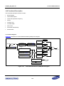
14 PULSE WIDTH MODULATION .................................................................14-1
14.1 Overview .............................................................................................................................................. 14-1
14.1.1 Features ........................................................................................................................................ 14-1
14.1.2 Pin Description.............................................................................................................................. 14-1
14.2 Functional Description ......................................................................................................................... 14-2
14.2.1 Block Diagram .............................................................................................................................. 14-2
14.2.2 General Description ...................................................................................................................... 14-3
14.2.3 Clock and Operation Frequency ................................................................................................... 14-4
14.2.4 Period ........................................................................................................................................... 14-4
14.2.5 PULSE Level ................................................................................................................................ 14-4
14.2.6 nPULSE Width .............................................................................................................................. 14-4
14.2.7 IDLE Level .................................................................................................................................... 14-5
14.2.8 Parameter Relationship ................................................................................................................ 14-5
14.2.9 Extension Bit ................................................................................................................................. 14-8
14.3 Register Description ........................................................................................................................... 14-13
14.3.1 Register Map Summary .............................................................................................................. 14-13
15 SERIAL PERIPHERAL INTERFACE (SPI) ................................................15-1
15.1 Overview .............................................................................................................................................. 15-1
15.1.1 Features ........................................................................................................................................ 15-1
15.1.2 Pin Description.............................................................................................................................. 15-2
15.2 Functional Description ......................................................................................................................... 15-3
15.2.1 Block Diagram .............................................................................................................................. 15-3
15.2.2 Operation ...................................................................................................................................... 15-4
15.3 Register Description ........................................................................................................................... 15-18
15.3.1 Register Map Summary .............................................................................................................. 15-18
16 TIMER/COUNTER .....................................................................................16-1
16.1 Overview .............................................................................................................................................. 16-1
16.1.1 Features ........................................................................................................................................ 16-1
16.1.2 Pin Description.............................................................................................................................. 16-2
16.2 Functional Description ......................................................................................................................... 16-3
16.2.1 Block Diagram .............................................................................................................................. 16-3
16.2.2 Counter Size ................................................................................................................................. 16-3
16.2.3 Counter Clock ............................................................................................................................... 16-4
16.2.4 Debug Option................................................................................................................................ 16-4
16.2.5 ADC Trigger Source ..................................................................................................................... 16-4
16.2.6 Overflow Mode.............................................................................................................................. 16-5
16.2.7 Period Mode ................................................................................................................................. 16-8
16.2.8 Interrupt ...................................................................................................................................... 16-17
16.3 Register Description ........................................................................................................................... 16-18
16.3.1 Register Map Summary .............................................................................................................. 16-18
17 UNIVERSAL SYNCHRONOUS/ASYNCHRONOUS
RECEIVER/TRANSMITTER ...........................................................................17-1
17.1 Overview .............................................................................................................................................. 17-1
17.1.1 Feature ......................................................................................................................................... 17-2
17.1.2 Pin Description.............................................................................................................................. 17-2
17.2 Functional Description ......................................................................................................................... 17-3
17.2.1 Block Diagram .............................................................................................................................. 17-3
17.2.2 BaudRate Generator .................................................................................................................... 17-4
17.2.3 General Description ...................................................................................................................... 17-4
17.3 Asynchronous Mode ............................................................................................................................ 17-5
17.3.1 Synchronous Mode ....................................................................................................................... 17-5
17.4 Receiver ............................................................................................................................................. 17-12
17.4.1 Asynchronous Receiver .............................................................................................................. 17-12
17.4.2 Synchronous Receiver ............................................................................................................... 17-13
17.5 Transmitter ......................................................................................................................................... 17-15
17.5.1 General Description .................................................................................................................... 17-15
17.5.2 Time-Guard................................................................................................................................. 17-16
17.5.3 Multi-Drop Mode ......................................................................................................................... 17-16
17.6 Break .................................................................................................................................................. 17-17
17.6.1 Transmit Break ........................................................................................................................... 17-17
17.6.2 Receive Break ............................................................................................................................ 17-17
17.6.3 Interrupts ..................................................................................................................................... 17-17
17.6.4 Test Modes ................................................................................................................................. 17-18
17.6.5 Smart Card Protocol ................................................................................................................... 17-18
17.6.6 Character Transmission to Smart Card ...................................................................................... 17-19
17.6.7 Character Reception from Smart Card ....................................................................................... 17-20
17.6.8 USART Configuration in Smart Card Mode ................................................................................ 17-20
17.7 Programming Examples ..................................................................................................................... 17-21
17.8 Register Description ........................................................................................................................... 17-22
17.8.1 Register Map Summary .............................................................................................................. 17-22
17.9 4 to 40 MHz Asynchronous Mode ...................................................................................................... 17-46
18 WATCHDOG TIMER..................................................................................18-1
18.1 Overview .............................................................................................................................................. 18-1
18.1.1 Feature ......................................................................................................................................... 18-1
18.2 Functional Description ......................................................................................................................... 18-2
18.2.1 Block Diagram .............................................................................................................................. 18-2
18.2.2 Watchdog Timer Functionality ...................................................................................................... 18-3
18.2.3 Watchdog Timer Events ............................................................................................................... 18-4
18.3 Register Description ............................................................................................................................. 18-5
18.3.1 Register Map Summary ................................................................................................................ 18-5
19 ELECTRICAL DATA..................................................................................19-1
19.1 Overview .............................................................................................................................................. 19-1
19.2 Absolute Maximum Ratings ................................................................................................................. 19-1
19.3 Recommended Operating Conditions .................................................................................................. 19-2
19.4 I/O Characteristics ............................................................................................................................... 19-3
19.5 I/O AC Electrical Characteristics .......................................................................................................... 19-4
19.6 Reset Input Characteristics .................................................................................................................. 19-5
19.7 External Interrupt Input Characteristics ............................................................................................... 19-6
19.8 Oscillator Characteristics ..................................................................................................................... 19-7
19.8.1 External Main Oscillator Characteristics ....................................................................................... 19-7
19.8.2 Internal Main Oscillator Characteristics ........................................................................................ 19-8
19.9 Current Consumption ........................................................................................................................... 19-9
19.10 PLL Characteristics .......................................................................................................................... 19-10
19.11 LVD Characteristics ......................................................................................................................... 19-11
19.12 12-bit ADC Electrical Characteristics ............................................................................................... 19-12
19.13 Comparator Electrical Characteristics ............................................................................................. 19-13
19.14 OP-AMP Electrical Characteristics .................................................................................................. 19-14
19.15 Flash Memory Characteristics ......................................................................................................... 19-15
19.16 SPI (SSP) Timing Characteristics .................................................................................................... 19-16
19.17 ESD Characteristics ......................................................................................................................... 19-17
20 PACKAGE SPECIFICATION .....................................................................20-1
20.1 Overview .............................................................................................................................................. 20-1
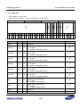
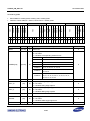
List of Figures
Figure
Number
Title
Page
Number
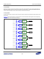
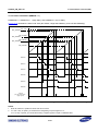
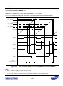
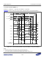
Figure 1-1
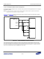
Block Diagram................................................................................................................................... 1-9
Figure 2-1
Figure 2-2
Figure 2-3
Figure 2-4
Figure 2-5
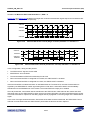
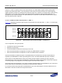
Pin Map Diagram .............................................................................................................................. 2-2
Pin Circuit Type A (P0.0 to P0.11 and P0.18 to P0.31) .................................................................. 2-11
Pin Circuit Type B (P0.12 to P0.17) ................................................................................................ 2-12
Pin Circuit Type C (MODE1 and MODE0) ...................................................................................... 2-12
Pin Circuit Type D (nRESET) ......................................................................................................... 2-13
Figure 3-1
S3FN429 Memory Map ..................................................................................................................... 3-1
Figure 4-1
Figure 4-2
Figure 4-3
Figure 4-4
Figure 4-5
Figure 4-6
Figure 4-7
Figure 4-8
Figure 4-9
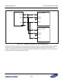
ADC Block Diagram .......................................................................................................................... 4-2
ADC Operation Timing Diagram ....................................................................................................... 4-4
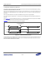
One-Shot Mode, Single Channel Conversion ................................................................................... 4-7
One-Shot Mode, Multi-Channel Conversion ..................................................................................... 4-7
Continuous Mode, Single-Channel Conversion ................................................................................ 4-8
Continuous Mode, Multi-Channel Conversion .................................................................................. 4-8
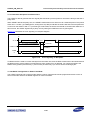
ADC Calibration Scheme ................................................................................................................ 4-11
2 Point Calibration .......................................................................................................................... 4-12
ADC Flowchart ................................................................................................................................ 4-14
Figure 5-1
Figure 5-2
Figure 5-3
Figure 5-4
Figure 5-5
Figure 5-6
Figure 5-7
Figure 5-8
Figure 5-9
Figure 5-10
Figure 5-11
Figure 5-12
Figure 5-13
Figure 5-14
Figure 5-15
Figure 5-16
Figure 5-17
Figure 5-18
Figure 5-19
Figure 5-20
Figure 5-21
Figure 5-22
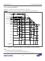
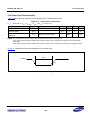
System Clock Tree Block Diagram ................................................................................................... 5-4
System Clock Selection .................................................................................................................... 5-5
Crystal/Ceramic Resonator or External Clock Circuit ....................................................................... 5-7
PLL (Phase-Locked Loop) Block Diagram ....................................................................................... 5-9
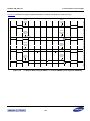
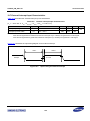
Clock Monitor Function ................................................................................................................... 5-11
External Main Oscillator Fail and Reset ......................................................................................... 5-12
End of Clock Fail ............................................................................................................................. 5-13
Clock Control State Machine .......................................................................................................... 5-14
The Change Clock Source of SYSCLK .......................................................................................... 5-15
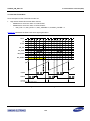
Instruction for IDLE and STOP ..................................................................................................... 5-18
Interrupt and Event ....................................................................................................................... 5-22
Different Handling Process for Interrupt and Event in IDLE or Stop Mode .................................. 5-23
External Interrupt Diagram ............................................................................................................ 5-25
Reset Sources .............................................................................................................................. 5-26
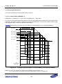
LVD Block Diagram ...................................................................................................................... 5-28
RESET@EMCLK .......................................................................................................................... 5-31
Start-Up with Basic Timer ............................................................................................................. 5-31
Fast Wake-Up ............................................................................................................................... 5-32
Basic Timer and Exit of Stop Mode when FWAKE is "0".............................................................. 5-32
Basic Timer and Exit of Stop Mode when FWAKE is "1" (SYSCLK = IMCLK) ............................. 5-33
Clock Initialization when Reset Value of SYSCLK is EMCLK ...................................................... 5-76
Clock Initialization when Reset Value of SYSCLK is IMCLK ........................................................ 5-77
Figure 6-1
Comparator Block Diagram .............................................................................................................. 6-3
Figure 7-1
Figure 7-2
Figure 7-3
Figure 7-4
Figure 7-5
PPD Block Diagram .......................................................................................................................... 7-2
Counter Operation (4 Multiplication Mode) ....................................................................................... 7-3
Counter Operation (1 Multiplication Mode) ....................................................................................... 7-4
Counter Operation (Type 1) .............................................................................................................. 7-5
Counter Operation (Type 2) .............................................................................................................. 7-5
Figure 9-1
Figure 9-2
Figure 9-3
Figure 9-4
Figure 9-5
Figure 9-6
Figure 9-7
Figure 9-8
Figure 9-9
Figure 9-10
Figure 9-11
Figure 9-12
Figure 9-13
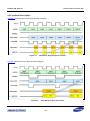
Flash Block Diagram (Non Pre-Fetch) .............................................................................................. 9-2
Flash Block Diagram (Pre-Fetch) ..................................................................................................... 9-2
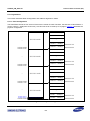
Physical Configuration ...................................................................................................................... 9-3
Normal Program Flowchart ............................................................................................................. 9-16
Page Erase Flowchart .................................................................................................................... 9-17
Sector Erase Flowchart .................................................................................................................. 9-18
Entire Erase Flowchart ................................................................................................................... 9-19
Smart Option Program Flowchart ................................................................................................... 9-20
Smart Option Erase Flowchart ........................................................................................................ 9-21
Error0 Condition ............................................................................................................................ 9-22
Error0 Condition ............................................................................................................................ 9-23
Error1 Condition ............................................................................................................................ 9-24
Error2 Condition ............................................................................................................................ 9-25
Figure 10-1
Figure 10-2
Figure 10-3
Figure 10-4
Figure 10-5
Figure 10-6
Figure 10-7
Figure 10-8
Figure 10-9
Figure 10-10
Figure 10-11
Figure 10-12
Figure 10-13
Figure 10-14
Figure 10-15
Figure 10-16
Figure 10-17
Figure 10-18
Figure 10-19
Figure 10-20
Figure 10-21
Figure 10-22
Figure 10-23
Figure 10-24
Figure 10-25
Figure 10-26
Figure 10-27
Figure 10-28
Figure 10-29
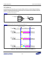
IMC Block Diagram ....................................................................................................................... 10-2
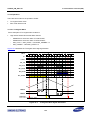
Tri-Angular Wave Signal Generation ............................................................................................ 10-3
Saw-Tooth Wave Signal Generation ............................................................................................ 10-4
Tri-Angular Wave (No SWAP, a Low Start PWMxUy, and High Start PWMxDy) ........................ 10-5
Tri-Angular Wave Duty (No SWAP, a Low Start PWMxUy, and High Start PWMxDy) ................ 10-6
Tri-Angular Wave (SWAP, a Low Start PWMxUy, and High Start PWMxDy) .............................. 10-7
Tri-Angular Wave Duty (SWAP, a Low Start PWMxUy, and High Start PWMxDy) ...................... 10-8
Tri-Angular Wave (No SWAP, a Low Start PWMxUy, and Low Start PWMxDy) ......................... 10-9
Tri-Angular Wave (SWAP, a Low Start PWMxUy, and Low Start PWMxDy) ............................. 10-10
Tri-Angular Wave (No SWAP, a High Start PWMxUy, and Low Start PWMxDy) .................... 10-11
Tri-Angular Wave Duty (No SWAP, a High Start PWMxUy, and Low Start PWMxDy) ............ 10-12
Tri-Angular Wave (SWAP, a High Start PWMxUy, and Low Start PWMxDy) .......................... 10-13
Tri-Angular Wave (No SWAP, a High Start PWMxUy, and High Start PWMxDy) .................... 10-14
Tri-Angular Wave (SWAP, a High Start PWMxUy, and High Start PWMxDy) ......................... 10-15
Saw-Tooth Wave (No SWAP, a Low Start PWMxUy, and High Start PWMxDy) ..................... 10-16
Saw-Tooth Wave Duty (No SWAP, a Low Start PWMxUy, and High Start PWMxDy) ............ 10-17
Saw-Tooth Wave (SWAP, a Low Start PWMxUy, and High Start PWMxDy) .......................... 10-18
Saw-Tooth Wave (No SWAP, a Low Start PWMxUy, and Low Start PWMxDy) ...................... 10-19
Saw-Tooth Wave (SWAP, a Low Start PWMxUy, and Low Start PWMxDy) ........................... 10-20
Saw-Tooth Save (No SWAP, a High Start PWMxUy, and Low Start PWMxDy) ...................... 10-21
Saw-Tooth Wave (SWAP, a High Start PWMxUy, and Low Start PWMxDy) .......................... 10-22
Saw-Tooth Wave (No SWAP, a High Start PWMxUy, and High Start PWMxDy) .................... 10-23
Saw-Tooth Wave (SWAP, a High Start PWMxUy, and High Start PWMxDy) .......................... 10-24
Synchronous Write at Zero and IMC_TCR Match (SYNCSEL = 00'b, NUMSKIP = 00000'b) . 10-33
Synchronous Write at Zero and IMC_TCR Match (SYNCSEL = 00'b, NUMSKIP = 00000'b) . 10-34
Synchronous Write at Zero Match (SYNCSEL = 01'b, NUMSKIP = 00000'b) ......................... 10-34
Synchronous Write at IMC_TCR Match (SYNCSEL = 10'b, NUMSKIP = 00000'b) ................. 10-35
Synchronous Write at Zero and IMC_TCR Match (SYNCSEL = 00'b, NUMSKIP = 00001'b) . 10-35
Synchronous Write at Zero Match (SYNCSEL = 01'b, NUMSKIP = 00001'b) ......................... 10-36
Figure 10-30
Figure 10-31
Synchronous Write at IMC_TCR Match (SYNCSEL = 10'b, NUMSKIP = 00001'b) ................. 10-36
Skip Control of ADC Trigger Signal Interrupt ............................................................................ 10-37
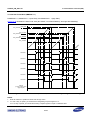
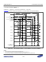
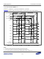
Figure 11-1
Interrupt Block Diagram ................................................................................................................ 11-4
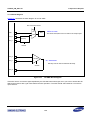
Figure 13-1
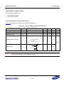
OP-AMP Block Diagram ............................................................................................................... 13-2
Figure 14-1
Figure 14-2
Figure 14-3
Figure 14-4
Figure 14-5
Figure 14-6
Figure 14-7
Figure 14-8
Figure 14-9
Pulse Width Modulation (PWM) Block Diagram ........................................................................... 14-2
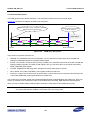
PWM Cycle Description ................................................................................................................ 14-3
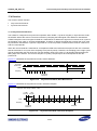
PWM Basic Waveform (OUTSL = 1, PWM Period = 0x40, Pulse = 0x0, 0x1, 0x20, 0x3F, 0x40) 14-6
PWM Basic Waveform (OUTSL = 0, PWM Period = 0x40, Pulse = 0x0, 0x1, 0x20, 0x3F, 0x40) 14-7
Extended PWM Waveform (PWM Period = 0x40, Pulse = 0x3E, PWMEX0) .............................. 14-9
Extended PWM Waveform (PWM Period = 0x40, Pulse = 0x3E, PWMEX1) ............................ 14-10
Extended PWM Waveform (PWM Period = 0x40, Pulse = 0x3E, PWMEX1 and PWMEX0) ..... 14-11
Extended PWM Waveform (High Start) ...................................................................................... 14-12
Extended PWM Waveform (Low Start) ....................................................................................... 14-12
Figure 15-1
Figure 15-2
Figure 15-3
Figure 15-4
Figure 15-5
Figure 15-6
Figure 15-7
Figure 15-8
Figure 15-9
SSP Block Diagram ...................................................................................................................... 15-3
Motorola SPI Frame Format (Single Transfer) with SPO = 0 and SPH = 0 ............................... 15-10
Motorola SPI Frame Format (Continuous Transfer) with SPO = 0 and SPH = 0 ....................... 15-11
Motorola SPI Frame Format with SPO = 0 and SPH = 1 ........................................................... 15-12
Motorola SPI Frame Format (Single Transfer) with SPO = 1 and SPH = 0 ............................... 15-13
Motorola SPI Frame Format (Continuous Transfer) with SPO = 1 and SPH = 0 ....................... 15-13
Motorola SPI Frame Format with SPO = 1 and SPH = 1 ........................................................... 15-14
PrimeCell SSP Master Coupled to Two Slaves .......................................................................... 15-15
SPI Master Coupled to two PrimeCell SSP Slaves .................................................................... 15-16
Figure 16-1
Figure 16-2
Figure 16-3
Figure 16-4
Figure 16-5
Figure 16-6
Figure 16-7
Figure 16-8
Figure 16-9
Figure 16-10
Figure 16-11
Figure 16-12
Figure 16-13
TC Block Diagram ......................................................................................................................... 16-3
Match and Overflow Operation Timing ......................................................................................... 16-5
Counter Values According to START, STOPCLEAR and STOPHOLD ....................................... 16-6
Capture Operation Timing ............................................................................................................ 16-7
Period Mode Timing ...................................................................................................................... 16-8
Interval Operation ......................................................................................................................... 16-9
PWM Operation .......................................................................................................................... 16-10
PWM Extension Waveform ......................................................................................................... 16-11
PWM Waveform with OUTSL = 0 ............................................................................................... 16-13
PWM Waveform with OUTSL = 1 ............................................................................................. 16-13
PWM Waveform Under IDLE State .......................................................................................... 16-15
PWM Waveform with STOPHOLD = 1, STOPCLEAR = 0 ....................................................... 16-15
PWM Waveform with STOPCLEAR = 1 ................................................................................... 16-16
Figure 17-1
Figure 17-2
Figure 17-3
Figure 17-4
Figure 17-5
Figure 17-6
Figure 17-7
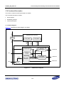
USART Block Diagram ................................................................................................................. 17-3
USART BaudRate Generator Block Diagram ............................................................................... 17-5
Asynchronous Mode, Start Bit Detection .................................................................................... 17-12
Asynchronous Mode, Character Reception ................................................................................ 17-12
Synchronous Mode, Character Reception .................................................................................. 17-13
IDLE Flag .................................................................................................................................... 17-14
Synchronous and Asynchronous Modes, Character Transmission............................................ 17-15
Figure 17-8
Figure 17-9
Smart Card Transmission Error .................................................................................................. 17-19
Error Signaling on Reception ...................................................................................................... 17-20
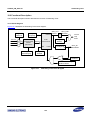
Figure 18-1
Watchdog Timer Block Diagram ................................................................................................... 18-2
Figure 19-1
Figure 19-2
Figure 19-3
Input Timing for nRESET .............................................................................................................. 19-5
Input Timing for External Interrupt ................................................................................................ 19-6
SPI Interface Transmit/Receive Timing ...................................................................................... 19-16
Figure 20-1
44-QFP-1010 Package Dimension ............................................................................................... 20-2
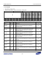
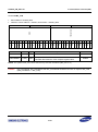
List of Tables
Table
Number
Title
Page
Number
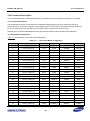
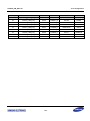
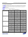
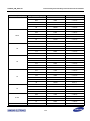
Table 2-1
Table 2-2
Table 2-3
Table 2-4
Table 2-5
Table 2-6
Table 2-7
Pin Assignment by Pin Number Order ............................................................................................... 2-3
Summary of Mirror Pins ..................................................................................................................... 2-5
Power Pin Description ........................................................................................................................ 2-6
System Pin Description ...................................................................................................................... 2-7
Function Pin Description .................................................................................................................... 2-9
Debug Interface Pin Description ...................................................................................................... 2-10
Flash Serial Program Pin Description .............................................................................................. 2-10
Table 3-1
Table 3-2
Table 3-3
S3FN429 Memory Map ...................................................................................................................... 3-1
Core Special Function Register Map ................................................................................................. 3-2
Peripheral Memory Map ..................................................................................................................... 3-3
Table 4-1
Table 4-2
Table 4-3
Table 4-4
ADC Pin Description .......................................................................................................................... 4-1
ADC Input and Digital Output ............................................................................................................. 4-3
CCNT Values and the Number of Conversions ................................................................................. 4-5
ICNUMx Value and Selected Input .................................................................................................... 4-6
Table 5-1
Table 5-2
Table 5-3
Table 5-4
Table 5-5
Table 5-6
Table 5-7
Table 5-8
Table 5-9
Table 5-10
Table 5-11
Table 5-12
Table 5-13
Table 5-14
Clock Definition .................................................................................................................................. 5-4
Summary of Smart Option for Clock Manager ................................................................................... 5-6
Clock Status at Reset and Wake-Up ................................................................................................. 5-6
Clock Monitor Control Bit ................................................................................................................. 5-11
Operation Mode Definition ............................................................................................................... 5-14
IDLE on Sleep-Now ......................................................................................................................... 5-20
IDLE on Sleep-on-Exit ..................................................................................................................... 5-20
Clock Status on STOP and Wake-Up .............................................................................................. 5-21
External Event Function ................................................................................................................... 5-24
Reset ID Flag ................................................................................................................................. 5-26
256 Counting Time by BT .............................................................................................................. 5-30
SYSCLK Divider Value .................................................................................................................. 5-60
PMS Value Table ........................................................................................................................... 5-64
The External Event Sources and Pin Assignment ......................................................................... 5-69
Table 6-1
Pin Description ................................................................................................................................... 6-1
Table 7-1
PPD Pin Description .......................................................................................................................... 7-1
Table 8-1
GPIO Pin Description ......................................................................................................................... 8-1
Table 9-1
Table 9-2
Flash Configuration ............................................................................................................................ 9-1
Base Address of Each Sector ............................................................................................................ 9-4
Table 9-3
Table 9-4
Table 9-5
Table 9-6
Table 9-7
Base Address of Each Page .............................................................................................................. 9-5
Configuration Smart Option Address and Control Bits ...................................................................... 9-6
Protection Smart Option Address and Control Bits ............................................................................ 9-8
Description of Interrupt Sources ...................................................................................................... 9-14
Pins Used to Read/Write/Erase the Flash ROM in Tool Program Mode ......................................... 9-15
Table 10-1
IMC Pin Description ....................................................................................................................... 10-1
Table 11-1
Table 11-2
Core Interrupt Vector ..................................................................................................................... 11-2
Device Interrupt Vector .................................................................................................................. 11-3
Table 12-1
I/O Function Mode Configuration ................................................................................................... 12-2
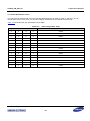
Table 13-1
Table 13-2
OP-AMP Pin Description ................................................................................................................ 13-1
Gain Configuration Table ............................................................................................................... 13-3
Table 14-1
Table 14-2
Table 14-3
PWM Pin Description ..................................................................................................................... 14-1
PERIOD and PULSE Field Relationship in Normal Mode ............................................................. 14-5
PWM Output................................................................................................................................... 14-6
Table 15-1
SSP Pin Description ....................................................................................................................... 15-2
Table 16-1
Table 16-2
Table 16-3
Pin Description ............................................................................................................................... 16-2
PWM Extension Bits .................................................................................................................... 16-11
PWM Output Polarity According to Control Bits ........................................................................... 16-14
Table 17-1
Table 17-2
Table 17-3
Table 17-4
USART Pin Description .................................................................................................................. 17-2
Asynchronous Mode (SYNC = 0) ................................................................................................... 17-6
Synchronous Mode (SYNC = 1) .................................................................................................... 17-9
Asynchronous Mode (SYNC = 0) ................................................................................................. 17-46
Table 19-1
Table 19-2
Table 19-3
Table 19-4
Table 19-5
Table 19-6
Table 19-7
Table 19-8
Table 19-9
Table 19-10
Table 19-11
Table 19-12
Table 19-13
Table 19-14
Table 19-15
Absolute Maximum Ratings ........................................................................................................... 19-1
Recommended Operating Conditions ............................................................................................ 19-2
I/O Characteristics ......................................................................................................................... 19-3
Reset Input Characteristics ............................................................................................................ 19-4
Reset Input Characteristics ............................................................................................................ 19-5
External interrupt Input Characteristics .......................................................................................... 19-6
External Main Oscillator Characteristics ........................................................................................ 19-7
Internal Main Oscillator Characteristics ......................................................................................... 19-8
Current Consumption at 5.5 V ....................................................................................................... 19-9
PLL Characteristics .................................................................................................................... 19-10
LVD Characteristics ................................................................................................................... 19-11
ADC Characteristics ................................................................................................................... 19-12
Comparator Electrical Characteristics ....................................................................................... 19-13
OP-AMP Electrical Characteristics ............................................................................................ 19-14
Flash Memory Characteristics ................................................................................................... 19-15
Table 19-16
Table 19-17
SPI Timing Characteristics ......................................................................................................... 19-16
ESD Characteristics ................................................................................................................... 19-17
Table 20-1
Package Specification Information................................................................................................. 20-1
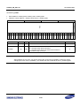
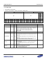
List of Conventions
Register RW Access Type Conventions
Type
Definition
Description
R
Read Only
The application has permission to read the Register field. Writes to read-only fields
have no effect.
W
Write Only
The application has permission to write in the Register field.
RW
Read & Write
The application has permission to read and writes in the Register field. The
application sets this field by writing 1'b1 and clears it by writing 1'b0.
Register Value Conventions
Expression
Description
x
Undefined bit
X
Undefined multiple bits
?
Undefined, but depends on the device or pin status
Device dependent
Pin value
The value depends on the device
The value depends on the pin status
Reset Value Conventions
Expression
Warning:
Description
0
Clears the register field
1
Sets the register field
x
Don't care condition
Some bits of control registers are driven by hardware or write operation only. As a result the indicated
reset value and the read value after reset might be different.
S3FN429_UM_REV1.20
1
1 Product Overview
Product Overview
1.1 Introduction
The S3FN429 user manual describes the complete reference specification of S3FN429.
The improved features of S3FN429 are:
ARM Cortex-M0 Core
Built-in 32 KB flash memory
Internal 2 KB SRAM for stack, data memory, or code memory
32 General Purpose IOs (GPIO)
Operating temperature: – 40 to 105 C
Operating voltage range: 2.5 to 5.5 V
Interrupt controller: Dynamically reconfigurable Nested Vectored Interrupt Controller (NVIC)
Clock and Power Management Controller (CM)
Watchdog Timer (WDT)
3 16-bit Timer/Counter (TC)
4 16-bit Pulse Width Modulation (PWM)
1 16-bit Pulse Position Decoder (PPD)
1 3-Phase Inverter Motor Controller (IMC)
1 USART, 1 SPI
12-bit Analog to Digital Converter (ADC) with external input AINx 10 Channel
1 Operational Amplifier (OP-AMP)
4 Comparator (COMP)
Supports idle and stop mode for reducing current
1-1
S3FN429_UM_REV1.20
1 Product Overview
1.2 Features
S3FN429 device contains:
CPU
Memory
Interrupt Controller
Clock Manager (CM)
Watchdog Timer (WDT)
16-bit Timer/Counter (TC)
Pulse Width Modulation (PWM)
Pulse Position Decoder (PPD)
Inverter Motor Controller (IMC)
Universal Synchronous/Asynchronous Receiver/Transmitter (USART)
Serial Peripheral Interface (SPI)
Analog to Digital Converter (ADC)
Operational Amplifier (OP-AMP)
Comparator (COMP)
General Purpose IO (GPIO)
Two Low Power Modes
Power-On Reset (POR)
Low Voltage Detection (LVD)
Phase-Locked Loop (PLL)
Operating Voltage Range
Operating Frequency Range
Operating Temperature Range
Available in 44 QFP Package
1-2
S3FN429_UM_REV1.20
1 Product Overview
CPU
The CPU contains:
32-bit RISC ARM Cortex-M0 Core
Serial Wire Debug (SWD)
Memory
The Memory supports:
32 KB internal program full flash
2 KB internal SRAM
Only little-endian
Interrupt Controller
The Interrupt Controller supports:
NVIC of Cortex-M0
Dynamically reconfigurable interrupt priority (four priority levels)
32 device interrupt vectors
Selectable eight External Interrupts EXI (n)
Programmable eight wake-up sources from stop
Clock Manager (CM)
The Clock Manager (CM) supports:
External Main Oscillator Clock (EMCLK) 1 to 12 MHz
Internal Main Oscillator Clock (IMCLK) 40 MHz
Phase-Locked Loop (PLL) control , from 12 to 40 MHz
Clock monitor to detect an external main oscillator failure
Low power mode (IDLE/STOP) by clock gating control
Programmable clock dividers (SDIV and PDIV)
Reset management
Basic timer for reset generation
1-3
S3FN429_UM_REV1.20
1 Product Overview
Watchdog Timer (WDT)
The Watchdog Timer (WDT) contains:
Configurable microcontroller reset event
Programmable 16-bit down counter
16-bit Timer/Counter (TC)
The 16-bit Timer/Counter (TC) contains:
Operation in an interval, capture, match, and overflow or PWM mode
Match and overflow interrupt
Selectable an internal or external clock
Pulse Width Modulation (PWM)
The Pulse Width Modulation (PWM) supports:
16-bit PWM signal generation
Interval mode
Programmable idle level
Extension PWM function
Pulse Position Decoder (PPD)
The Pulse Position Decoder (PPD) contains:
3 input signals are:
PHASEA
PHASEB
PHASEZ
Position counter and position capture timer
Speed counter and speed capture timer
Up/Down counter
1-4
S3FN429_UM_REV1.20
1 Product Overview
Inverter Motor Controller (IMC)
The Inverter Motor Controller (IMC) supports:
3-Phase 16-bit PWM generation
Programmable dead time insertion
Output off-control by fault input signals
ADC conversion start signal generation
Universal Synchronous/Asynchronous Receiver/Transmitter (USART)
The Universal Synchronous/Asynchronous Receiver/Transmitter (USART) supports:
5, 6, 7, 8 and 9-bit data length
Programmable baud rate generator
Parity, framing, and overrun error detection
Loop-back mode
Full duplex
Idle flag for J1587 protocol
Smart-card protocol: error signaling and re-transmission
Serial Peripheral Interface (SPI)
The Serial Peripheral Interface (SPI) supports:
Programmable data frame from 4 to 16-bit
Master and slave mode
Programmable clock pre-scale
Separate 8/8 16-bit width Transmit/Receive First-In First-Out (FIFO)
Analog to Digital Converter (ADC)
The Analog to Digital Converter (ADC) contains:
12-bit resolution
10 input pins for conversion input signal, AIN[10:1]
ADC has a conversion channel for OP-AMP (AIN0)
Various conversion start sources - START (software), ADTRG (external input signal), and internal peripherals
(IMC, Timer)
1-5
S3FN429_UM_REV1.20
1 Product Overview
Operational Amplifier (OP-AMP)
The Operational Amplifier (OP-AMP) supports:
The operation with ADC
Both an internal and external gain control
Comparator (COMP)
The Comparator contains:
Configurable reference voltage selection
Control signal for IMC output or input signal for PPD
General Purpose IO (GPIO)
The General Purpose IO (GPIO) contains:
Input or Output configuration
Output open-drain/push-pull configuration
GPIO interrupt
Low Power Modes
The Two Low Power Mode supports:
IDLE: Only CPU clock stops
STOP: All clocks stop
Fast wake-up with internal main oscillator (from stop mode to normal mode)
Programmable external event/interrupt sources for wake-up
Power-On Reset (POR)
The Power-On Reset (POR) contains:
Built-in POR circuit
1-6
S3FN429_UM_REV1.20
1 Product Overview
Low Voltage Detection (LVD)
The Low Voltage Detection (LVD) contains:
LVD for reset with configurable voltage levels
LVD for interrupt with configurable voltage levels
LVD reset/interrupt enable/disable can be controllable
Phase-Locked Loop (PLL)
The Phase-Locked Loop (PLL) contains:
Input clock source: EMCLK
Input frequency: 1 to 12 MHz
Output frequency: 12 to 40 MHz
Operating Voltage Range
The Operating Voltage Range contains:
2.5 to 5.5 V
Operating Frequency Range
The Operating Frequency Range contains:
Up to 40 MHz
EMCLK: 1 to 12 MHz
IMCLK: 40 MHz
PLL clock: 12 to 40 MHz
Operating Temperature Range
The Operating Temperature Range contains:
– 40 C to 105 C
1-7
S3FN429_UM_REV1.20
1 Product Overview
Package
The Package contains:
Available in 44-QFP
Width Length: 10.0 mm 10.0 mm
Lead pitch: 0.8 mm
1-8
S3FN429_UM_REV1.20
1 Product Overview
1.3 Block Diagram
SWDBG
sleep
CM0
Core
debug
Systick
Data
Peripheral IRQ
Cortex -M0
Interrupts
Inst
N
V
I
C
I INTMI
W INTISR
D
SWJ-DP
G
P
I
O
I/Os Conf
Figure 1-1 illustrates the block diagram of S3FN429 device.
DWP
ITM
TPIU
Cortex -M0
APB
AHB-AP
APB
SRAM
2KB
Contorller
AHB2APB
AHB
Internal Flash
32KB
IFController
WDT
nRESET
CM
LVD
16-bit TC1
EMCLK (1 to 12MHz)
16-bit TC2
PLLCLK (12 to 40MHz)
USART0
IMC
U, /U
V, /V
W, /W
SP10
PWM0
PPD
PWM1
PhaseA
PhaseB
PhaseZ
PWM2
PWM3
12-bit ADC: 10 ch
Comparator0
Comparator1
Comparator2
OP-AMP0
Comparator3
I/Os conf
Figure 1-1
1-9
Block Diagram
G
P
I
O
I/O Conf
I/O Conf
XIN
XOUT
IMCLK (40MHz)
16-bit TC0
G
P
I
O
POR
S3FN429_UM_REV1.20
2
2 Pin Configuration
Pin Configuration
2.1 Overview
The Pin Configuration chapter describes the pin information of S3FN429.
This chapter includes:
Pin map diagram
Pin assignment table
Mirror pins
Pin description
Power pins
System pins
Function pins
Debug interface pins
Flash serial program pins
Pin circuit type
Type A
Type B
Mode pins
nReset pin
2-1
S3FN429_UM_REV1.20
2 Pin Configuration
2.2 Pin Map
44
43
42
41
40
39
38
37
36
35
34
PLLCAP
P0.29/COMP3_P/EXI21/SWDCLK
P0.28/COMP3_N/EXI20/SWDIO
P0.27/COMP2_P/USARTTX0/EXI19
P0.26/COMP2_N/USARTRX0/EXI18
P0.25/COMP1_P/FSS0/COP4
P0.24/COMP1_N/SCLK0/PWM2
P0.23/COMP0_P/MOSI0/PWM1
P0.22/COMP0_N/MISO0/EXI17
P0.21/PHASEZ/USARTCLK0/EXI16
P0.20/PHASEB/USARTTX0/EXI15
Figure 2-1 illustrates the pin map for S3FN429 device.
1
2
3
4
5
6
7
8
9
10
11
S3FN429
(40-QFP)
33
32
31
30
29
28
27
26
25
24
23
P0.3/AIN2/PWM0/EXI2
P0.4/AIN3/PWM1/EXI3
P0.5/AIN4/PWM2/EXI4
P0.6/AIN5/PWM3/EXI5
P0.7/AIN6/PWM0/TPWM1
P0.8/AIN7/PWM1/TCAP1
P0.9/AIN8/PWM2/TCLK1
P0.10/AIN9/PWM3/EXI6
P0.11/AIN10/USARTCLK0/ADTRG
AVREF
AVSS
12
13
14
15
16
17
18
19
20
21
22
MODE1
MODE0
nRESET
VSSCORE
VDDCORE
VDDCOREOUT
XOUT/P0.30/ - /USARTTX0/EXI22
XIN/P0.31/EXI23/USARTRX0/PWM0
P0.0/EXI0/TPWM0/OP0_N
P0.1/EXI1/TCAP0/OP0_P
P0.2/AIN1/TCLK0/OP0_O
Figure 2-1
Pin Map Diagram
NOTE: If you use OP amp, AIN1 should not be used for ADC input.
2-2
P0.19/PHASEA/USARTRX0/EXI14
P0.18/PWMOFF/COP3/EXI13
VDDIO
VSSIO
P0.17/PWMD0/COP2/EXI12
P0.16/PWMD1/COP1/EXI11
P0.15/PWMD2/COP0/EXI10
P0.14/PWMU0/TCLK2/EXI9/F_SDAT
P0.13/PWMU1/TCAP2/EXI8/F_SCLK
P0.12/PWMU2/TPWM2/EXI7
AVDD
S3FN429_UM_REV1.20
2 Pin Configuration
2.3 Pin Assignment
Table 2-1 describes the pin assignment details.
Table 2-1
Pin Assignment by Pin Number Order
Pin
Number
1
1
MODE1
MODE1
2
MODE0
3
st
nd
rd
2
3
th
4
Flash
MODE1
MODE1
MODE1
MODE0
MODE0
MODE0
MODE0
nRESET
nRESET
nRESET
nRESET
nRESET
4
VSSCORE
VSSCORE
VSSCORE
VSSCORE
VSSCORE
5
VDDCORE
VDDCORE
VDDCORE
VDDCORE
VDDCORE
6
VDDCOREOUT
VDDCOREOUT
VDDCOREOUT
VDDCOREOUT
VDDCOREOUT
7
XOUT/P0.30
XOUT/–
XOUT/USARTTX0
XOUT/EXI22
–
8
XIN/P0.31
XIN/EXI23
XIN/USARTRX0
XIN/PWM0
–
9
P0.0
EXI0
TPWM0
OP0_N
–
10
P0.1
EXI1
TCAP0
OP0_P
–
11
P0.2
AIN1
TCLK0
OP0_O
–
12
P0.3
AIN2
PWM0
EXI2
–
13
P0.4
AIN3
PWM1
EXI3
–
14
P0.5
AIN4
PWM2
EXI4
–
15
P0.6
AIN5
PWM3
EXI5
–
16
P0.7
AIN6
PWM0
TPWM1
–
17
P0.8
AIN7
PWM1
TCAP1
–
18
P0.9
AIN8
PWM2
TCLK1
–
19
P0.10
AIN9
PWM3
EXI6
–
20
P0.11
AIN10
USARTCLK0
ADTRG
–
21
AVREF
AVREF
AVREF
AVREF
–
22
AVSS
AVSS
AVSS
AVSS
–
23
AVDD
AVDD
AVDD
AVDD
–
24
P0.12
PWMU2
TPWM2
EXI7
–
25
P0.13
PWMU1
TCAP2
EXI8
F_SCLK
26
P0.14
PWMU0
TCLK2
EXI9
F_SDAT
27
P0.15
PWMD2
COP0
EXI10
–
28
P0.16
PWMD1
COP1
EXI11
–
29
P0.17
PWMD0
COP2
EXI12
–
30
VSSIO
VSSIO
VSSIO
VSSIO
VSSIO
31
VDDIO
VDDIO
VDDIO
VDDIO
VDDIO
32
P0.18
PWMOFF
COP3
EXI13
–
2-3
S3FN429_UM_REV1.20
2 Pin Configuration
Pin
Number
1
33
P0.19
PHASEA
USARTRX0
EXI14
–
34
P0.20
PHASEB
USARTTX0
EXI15
–
35
P0.21
PHASEZ
USARTCLK0
EXI16
–
36
P0.22
COMP0_N
MISO0
EXI17
–
37
P0.23
COMP0_P
MOSI0
PWM1
–
38
P0.24
COMP1_N
SCLK0
PWM2
–
39
P0.25
COMP1_P
FSS0
COP4
–
40
P0.26
COMP2_N
USARTRX0
EXI18
–
41
P0.27
COMP2_P
USARTTX0
EXI19
–
42
P0.28
COMP3_N
EXI20
SWDIO
–
43
P0.29
COMP3_P
EXI21
SWDCLK
–
44
PLLCAP
PLLCAP
PLLCAP
PLLCAP
–
st
nd
rd
2
3
2-4
th
4
Flash
S3FN429_UM_REV1.20
2 Pin Configuration
2.4 Mirror Pins
Several pins have mirror pins. This helps in flexibility in arranging. These pins are, however, defined for one
instance (IP) only.
Table 2-2 describes the summary of mirror pins.
Table 2-2
Summary of Mirror Pins
IP (Instance)
Pin
PWM0
P0.31/EXI23/USARTRX0/PWM0
P0.3/AIN2/PWM0/EXI2
P0.7/AIN6/PWM0/TPWM1
PWM1
P0.4/AIN3/PWM1/EXI3
P0.8/AIN7/PWM1/TCAP1
P0.23/COMP0_P/MOSI0/PWM1
PWM2
P0.5/AIN4/PWM2/EXI4
P0.9/AIN8/PWM2/TCLK1
P0.24/COMP1_N/SCLK0/PWM2
PWM3
P0.6/AIN5/PWM3/EXI5
P0.10/AIN9/PWM3/EXI6
USART0
P0.30/–/USARTTX0/EXI22
P0.31/EXI23/USARTRX0/PWM0
P0.11/AIN10/USARTCLK0/ADTRG
P0.19/PHASEA/USARTRX0/EXI14
P0.20/PHASEB/USARTTX0/ExI15
P0.21/PHASEZ/USARTCLK0/EXI16
P0.26/COMP2_N/USARTRX0/EXI18
P0.27/COMP2_P/USARTTX0/EXI19
2-5
S3FN429_UM_REV1.20
2 Pin Configuration
2.5 Pin Description
The pin description section describes:
Power Pins
System Pins
Function Pins
Debug Interface Pins
Flash Serial Program Pins
NOTE:
1.
D/A: Digital or Analog, D: Digital, A: Analog
2.
I/O: Input or Output, I: Input, O: Output
3.
PIN[Z:A]: The same function pin group, PIN.A, PIN.B, to ,PIN.Z
2.5.1 Power Pins
Table 2-3 describes the power pin description.
Table 2-3
Module
Power
Pin Name
Power Pin Description
Function Description
Comments
VDDCORE
Core DC Supply Voltage
See recommended operating condition
VSSCORE
Core Ground Voltage
VDDIO
I/O DC Supply Voltage
VSSIO
I/O Ground Voltage
AVDD
ADC Supply Voltage
AVSS
ADC Ground Voltage
–
AVREF
ADC Reference Input Voltage
–
VDDCOREOUT
Cap Output Port from Internal
Regulator
Connected to GND through a 0.1 F
capacitor (From internal regulator)
PLLCAP
Cap Output Port for PLL
Connected to GND through a 220 pF
capacitor for PLL
–
See recommended operating condition
–
See recommended operating condition
2-6
S3FN429_UM_REV1.20
2 Pin Configuration
2.5.2 System Pins
Table 2-4
Module
RESET
Pin Name
Function
D/A
I/O
nRESET
Hardware Reset Input
This nRESET pin contains an internal pull up resistor
typical 250 k. Setting this pin to low level initialize the
internal state of the device. Thereafter, setting the input
to high release the reset status. The S3FN429 waits for
the system clock to be stabled, and the PC to the reset
interrupt vector. Internal Reset is generated after clock
stabilization.
D
I
XIN (1)
External Main Oscillator Input
A
I
–
XOUT (2)
External Main Oscillator Output
A
O
–
COP[4:0]
Internal Clock Out Port
COP0 = EMCLK/8
COP1 = IMCLK/8
COP2 = PLLCLK/8
COP3 = CORECLK/8
COP4 = PCLK/8
These pins help you to check clock status when your
system has some problem or you are sure about
programmed clock configuration.
D
O
–
MODE1
Mode Selection
MODE1 is for a factory test, so it should be connected
with ground in user mode.
D
I
Internal
pull-down
D
I
Internal
pull-down
CM
MODE
MODE0
Caution:
System Pin Description
This pin decides either normal mode or tool mode. If onboard writing (programming in tool mode) is needed,
0.1 uF capacitor should be connected between MODE0
pin and ground. Parallel 1 k resistor should be
connected for better noise immunity. (3)
But if you use S3FN429 only in normal mode without
on-board writing, this pin should be connected to
ground directly.
Mode 1
Mode 0
0
0
Normal Mode
0
1
Tool Mode
Comments
Internal filter
Mode Setting
If you don't the external main-oscillator when pin7 and pin8 are defined XOUT and XIN function, you
should tie XIN to ground. XOUT should be opened.
2-7
S3FN429_UM_REV1.20
2 Pin Configuration
NOTE:
1.
After reset, the default function of pin8 can be one of two. One is XIN, the other is P0.30. The hardware reset condition
is decided by smart option. That means you need to program the chip configuration smart option if you want to change
that pin's reset function. You can program and erase the smart option in normal or tool mode. Refer to Chapter 9. Internal
Flash Controller IFC).
2.
After reset, the default function of pin7 can be one of two. One is XOUT, the other is P0.31. The hardware reset condition
is decided by smart option. That means you need to program the chip configuration smart option if you want to change
that pin's reset function. You can program and erase the smart option in normal or tool mode. Refer to Chapter 9. Internal
Flash Controller (IFC).
3.
MODE0
1KΩ
0.1uF
2-8
S3FN429_UM_REV1.20
2 Pin Configuration
2.5.3 Function Pins
Table 2-5 describes pin description.
Table 2-5
Module
Pin Name
Function Pin Description
Function
D/A
I/O
Comments
Multiplexed with
peripheral module
GPIO
P0[31:0]
General purpose I/O multiplexed
D
I/O
Interrupt
EXI[23:0]
External interrupt request
D
I
–
TCLK[2:0]
External clock input for timer
D
I
–
TCAP[2:0]
Capture input for timer
D
I
–
TPWM[2:0]
PWM output for timer
D
O
–
PWM[3:0]
Pulse width modulation output
D
O
–
PWMU[2:0]
PWM output for inverter motor
D
O
–
PWMD[2:0]
PWM output for inverter motor
D
O
–
PWMOFF
Input pin for PWM output off
D
I
–
PHASEA
Phase A input
D
I
–
PHASEB
Phase B input
D
I
–
PHASEZ
Phase Z input
D
I
–
SCLK0
SPI serial clock
D
I/O
–
MISO0
Master in slave out
D
I/O
–
MOSI0
Master out slave in
D
I/O
–
FSS0
Frame or slave select (master)
frame input (slave)
D
I/O
–
USARTRX0
Received signal input
D
I
–
USARTTX0
Transmit signal output
D
O
–
USARTCLK0
Clock signal
D
I/O
–
AIN[10:1]
Analog Input channels
A
I
–
ADTRG
ADC external Trigger input pin
D
I
–
OP0_N
OP-AMP negative input
A
I
–
OP0_P
OP-AMP positive input
A
I
–
OP0_O
OP-AMP out
A
O
–
COMP[3:0]_N
Comparator negative input
A
I
–
COMP[3:0]_P
Comparator positive input
A
I
–
16-bit timer
PWM
IMC
PPD
SPI
USART
ADC
OP-AMP
Comparator
2-9
S3FN429_UM_REV1.20
2 Pin Configuration
2.5.4 Debug Interface Pins
Table 2-6
Module
DEBUG
Debug Interface Pin Description
Pin Name
Function
D/A
I/O
SWDIO
Select/serial wire data input output
D
I/O
SWDCLK
Serial wire clock
D
I
Comments
Internal pull-up 55 k
–
2.5.5 Flash Serial Program Pins
Table 2-6 describes pin description. Refer to 9.2.3.2 Tool Program Mode for more details.
Table 2-7
Module
FLASH
Pin Name
Flash Serial Program Pin Description
Function
D/A
I/O
F_SDAT
Serial Data pin
(output when reading, input when writing)
–
I/O
F_SCLK
Serial Clock
–
I
2-10
Comments
Input and push-pull
output
–
S3FN429_UM_REV1.20
2 Pin Configuration
2.6 Pin Circuit Type
2.6.1 Block Diagram
Figure 2-2, Figure 2-3, Figure 2-4, and Figure 2-5 illustrate the Type A, Type B, MODEx and nRESET pin circuits
respectively.
2.6.1.1 Type A
Bi-directional buffer with B4 (NOTE) output driver and enables schmitt trigger cmos input with controllable 55K pullup resistor and 250 analog input. The status of input data is high when this is an output mode.
NOTE: B4: Output Max. Operation Freq. 8 MHz
PAD
Output Data
Output Enable
Pull-up Enable
Input Enable
Input Data
Analog In/Output
Figure 2-2
Pin Circuit Type A (P0.0 to P0.11 and P0.18 to P0.31)
2-11
S3FN429_UM_REV1.20
2 Pin Configuration
2.6.1.2 Type B
Bi-directional buffer with Iol = 24 mA (@1 V in 5 V operation at 25 C) output driver and enables schmitt trigger
cmos input with controllable 55K pull-up resistor and 250 analog input.
PAD
Output Data
Output Enable
Pull-up Enable
Input Enable
Input Data
Analog In/Output
Figure 2-3
Pin Circuit Type B (P0.12 to P0.17)
2.6.1.3 MODE1 and MODE0
Schmitt trigger cmos input with 55K pull-down resistor
Input Data
PAD
55Kohm
Figure 2-4
Pin Circuit Type C (MODE1 and MODE0)
2-12
S3FN429_UM_REV1.20
2 Pin Configuration
2.6.1.4 nRESET
Bi-directional buffer with B8 (NOTE) output driver and enable schmitt trigger cmos input with always 250K pull-up
resistor.
NOTE: B8: Output Max. Operating Freq. 15 MHz
PAD
Output Data
Output Enable
Input Enable
Input Data
Figure 2-5
Pin Circuit Type D (nRESET)
2-13
S3FN429_UM_REV1.20
3
3 System Memory Management
System Memory Management
3.1 Overview
The System Memory Management chapter describes the system memory management for S3FN429.
The chapter includes:
Memory map
Special function register map. The register maps are:
Core special function register map
Peripheral special function register map
3.2 Default Memory Map
Table 3-1 describes the S3FN429 memory space allocation.
Table 3-1
S3FN429 Memory Map
Address
Memory
Reserved
Reserved
0xE00F_FFFF to 0xE000_0000
Cortex-M0 internal peripheral registers
Reserved
Reserved
0x400F_FFFF to 0x4000_0000
Special function registers
Reserved
Reserved
0x2000_07FF to 0x2000_0000
2 KB internal SRAM memory
Reserved
Reserved
0x0000_7FFF to 0x0000_0000
32 KB internal program flash memory (Including smart option area)
3-1
S3FN429_UM_REV1.20
3 System Memory Management
Reserved
0xE00F_FFFF
~
0xE000_0000
Cortex-M0 Internal Peripheral Registers
Reserved
0x400F_FFFF
~
0x4000_0000
Special Function Registers
Reserved
0x2000_07FF
~
0x2000_0000
2Kbytes Internal SRAM Memory
Reserved
0x0000_7FFF
~
0x0000_00C4 ···(a)
0x0000_00C0 ···(b)
~
0x0000_0000
32Kbytes Internal Flash Memory
(a) Protection Smart Option
(b) Configuration Smart Option
Figure 3-1
S3FN429 Memory Map
3-1
S3FN429_UM_REV1.20
3 System Memory Management
3.3 Special Function Register Map
The two types of special function register maps are:
Core special function register map
Peripheral special function register map
3.3.1 Core Special Function Register Map
Table 3-2 describes the core special function register map.
Table 3-2
Core Special Function Register Map
Base Address
Peripheral
Description
0xE00F_F000
ROM Table
ROM Memory Table
0xE004_2000
External PPB
Private Peripheral Bus
0xE004_1000
Reserved
0xE004_0000
TPIU
0xE000_F000
Reserved
0xE000_E000
SCS
0xE000_3000
Reserved
0xE000_2000
FPB
Flash Patch and Break Pint
0xE000_1000
DWT
Data Watch Point and Trace
0xE000_0000
ITM
Instrumentation Trace Macro-cell
–
Trace Port Interface
–
System Control Space
–
3-2
S3FN429_UM_REV1.20
3 System Memory Management
3.3.2 Peripheral Special Function Register Map
Table 3-3 describes the peripheral special function register map.
Table 3-3
Module
Peripheral Memory Map
Base Address
Peripheral
PPD
0x400C_0000
PPD
Pulse Position Decoder
IMC
0x400B_0000
IMC
Inverter Motor Controller
SPI
0x4009_0000
SPI
Serial Peripheral Interface
USART
0x4008_0000
USART
Universal Synchronous/Asynchronous Receiver/Transmitter
0x4007_3000
PWM3
Pulse Width Modulation 3 (16-bit)
0x4007_2000
PWM2
Pulse Width Modulation 2 (16-bit)
0x4007_1000
PWM1
Pulse Width Modulation 1 (16-bit)
0x4007_0000
PWM0
Pulse Width Modulation 0 (16-bit)
0x4006_2000
TC2
Timer/Counter 2 (16-bit)
0x4006_1000
TC1
Timer/Counter 1 (16-bit)
0x4006_0000
TC0
Timer/Counter 0 (16-bit)
0x4005_8000
IOCONF
0x4005_0000
GPIO0
General Purpose IO Group 0
Comparator
0x4004_2000
COMP
Comparator
OP-AMP
0x4004_1000
OP-AMP
ADC
0x4004_0000
ADC
Analog to Digital Converter
WDT
0x4003_0000
WDT
Watchdog Timer (16-bit)
SYSTEM
0x4002_0000
CM
Clock Manager
MEMORY
0x4001_0000
IFC
Internal Flash Controller
PWM
TC
GPIO
Description
IO Configuration
Operational Amplifier
3-3
S3FN429_UM_REV1.20
4
4 Analog to Digital Converter (ADC)
Analog to Digital Converter (ADC)
4.1 Overview
This chapter describes the complete functional description of the Analog to Digital Converter (ADC) controller and
the operation of design from the end user perspective.
4.1.1 Features
The distinctive features of ADC are:
Resolution: 12-bit
One input channel (AIN0) is assigned to Operational Amplifier (OP-AMP)
10 external input channels, AIN[10:1]
Conversion start sources
Software start
External trigger input (ADTRG)
Internal peripheral trigger signals (Inverter Motor Controller (IMC) and Timer/Counter (TC))
Maximum conversion rate: 5 MHz clock
Analog input voltage range: 0 to VAVREF
Differential linearity error: 1.5 LSB (Max.) at 2.5 to 5.5 V
Integral linearity error: 3.5 LSB (Max.) at 2.5 to 5.5 V
4.1.2 Pin Description
Table 4-1 describes the pin description of ADC.
Table 4-1
Pin Name
ADC Pin Description
Function
I/O Type
Comments
AVREF
Reference top voltage
Analog Input
–
AIN[10:1]
Analog inputs
Analog Input
–
ADTRG
External start trigger signal
Digital Input
–
NOTE: You should write "AIN1" value in ICNUM field of CCSRx register to convert analog signal asserted on AIN1 pin.
4-1
S3FN429_UM_REV1.20
4 Analog to Digital Converter (ADC)
4.1.3 Block Diagram
Figure 4-1 illustrates the block diagram of ADC.
AIN1
AIN2
AIN3
AIN4
AIN5
AIN6
AIN7
AIN8
AIN9
AIN10
12-bit
ADC
Calibration
ADC_OCR
Conversion Channel Select MUX
OPA_N OPAMP
SHA
OPA_P
ADC_CBR0
ADC_CRR0[11:0]
ADC_CBR1
ADC_CRR1[11:0]
ADC_CBR2
ADC_CRR2[11:0]
ADC_CBR3
ADC_CRR3[11:0]
ADC_CBR4
ADC_CRR4[11:0]
ADC_CBR5
ADC_CRR5[11:0]
ADC_CBR6
ADC_CRR6[11:0]
ADC_CBR7
ADC_CRR7[11:0]
ADC_CBR8
ADC_CRR8[11:0]
ADC_CBR9
ADC_CRR9[11:0]
ADC_CBR10
ADC_CRR10[11:0]
ADC_IMSCR.x
ADC_MR.CCNT
ADC_CCSR0.ICNUM[7:0]
Interrupt
controller
ADC_CCSR1.ICNUM[10:8]
ADC_MR[x.x]
START(S/W)
SOC
ADTRG
Timer
IMC ADCTrigger
Figure 4-1
ADC Block Diagram
4-2
INT_OVR
INT_EOC
S3FN429_UM_REV1.20
4 Analog to Digital Converter (ADC)
4.1.4 Input and Output
ADC operation converts the signal asserted on AINx input pin to digital data. The valid input signals are:
Voltage range is from reference bottom to Top. ADC uses AINx function pins to convert an analog input
source.
Input signal range is from reference top to reference bottom.
Input Voltage Range: 0.0 V – VAVREF
Reference Bottom = 0.0 V
Reference Top = VAVREF
VAVREF can be from 2.5 to 5.5 V (typical 5 V).
Assume VAVREF = 5 V.
1 LSB
=
Reference Top - Reference Bottom
2
Resolution
=
5.0V - 0.0V
2
12
=
5.0V
4096
≈
1.22mV
Table 4-2 describes the ADC Input and digital Output values.
Table 4-2
ADC Input and Digital Output
Index
AINx Input Voltage (V)
Digital Output (Binary)
Digital Output (HEX)
0
– 0.001220703
0000 0000 0000
0x000
1
0.001221 to 0.002441406
0000 0000 0001
0x001
2
0.002441 to 0.003662109
0000 0000 0010
0x002
–
–
–
–
4093
4.996338 – 4.997558594
1111 1111 1101
–
4094
4.997559 – 4.998779297
1111 1111 1110
0xFFE
4095
4.998779 to
1111 1111 1111
0xFFF
4-3
S3FN429_UM_REV1.20
4 Analog to Digital Converter (ADC)
4.1.5 Clock Frequency and Conversion Time
ADC operation obtains clock from PCLK. ADC clock is not more than 5 MHz. This feature is effective up to a 5
MHz maximum ADC clock. If ADC operates with 5 MHz, the conversion per channel is done in the minimum time
(1 s).
Figure 4-2 illustrates the ADC operation timing.
Disable
TS
Enable
AINx Conversion
Enable
ADCEN
START Trigger
BUSY
EOC
Access CRRx
Figure 4-2
ADC Operation Timing Diagram
4-4
S3FN429_UM_REV1.20
4 Analog to Digital Converter (ADC)
4.1.6 Conversion Mode
This section describes Conversion Mode and Sequence of ADC.
4.1.6.1 Conversion Sequence
A conversion sequence is a sequence of conversion of analog inputs. You can configure ADC block to make
conversions of some of the 10 inputs and an input by OP-AMP in its own order. The setting of the CCNT field in
the ADC Mode Register (ADC_MR) defines the length of the sequence (the number of conversions).
Table 4-3 describes the relation between the CCNT field and the number of conversion performed in a sequence.
Table 4-3
CCNT Values and the Number of Conversions
CCNT[3:0]
Count Value
Description
0000
1
One conversion operation of ICNUM0[3:0]
0001
2
2 times conversion operation from ICNUM0[3:0] to ICNUM1[3:0]
0010
3
3 times conversion operation from ICNUM0[3:0] to ICNUM2[3:0]
0011
4
4 times conversion operation from ICNUM0[3:0] to ICNUM3[3:0]
0100
5
5 times conversion operation from ICNUM0[3:0] to ICNUM4[3:0]
0101
6
6 times conversion operation from ICNUM0[3:0] to ICNUM5[3:0]
0110
7
7 times conversion operation from ICNUM0[3:0] to ICNUM6[3:0]
0111
8
8 times conversion operation from ICNUM0[3:0] to ICNUM7[3:0]
1000
9
9 times conversion operation from ICNUM0[3:0] to ICNUM8[3:0]
1001
10
10 times conversion operation from ICNUM0[3:0] to ICNUM9[3:0]
1010
11
11 times conversion operation from ICNUM0[3:0] to ICNUM10[3:0]
4-5
S3FN429_UM_REV1.20
4 Analog to Digital Converter (ADC)
When configured in "one shot" mode, the ADC performs the specified number of conversion after a start request.
At the end of each conversion sequence, the data register gets updated with the conversion result.
You can program the conversion of a sequence in ADC_CCSR0 and ADC_CCSR1 (Conversion Channel
Sequence Register). The ICNUM0 field defines the first input conversion in sequence. The ICNUM1 field defines
the second input conversion and this sequence continues.
Table 4-4 describes the relation between the ICNUMx values and input selected.
Table 4-4
ICNUMx Value and Selected Input
ICNUMx Values
Selected Pin
0000
AIN 0 for op-amp
0001
AIN 1
0010
AIN 2
0011
AIN 3
0100
AIN 4
0101
AIN 5
0110
AIN 6
0111
AIN 7
1000
AIN 8
1001
AIN 9
1010
AIN 10
For example, assume:
CCNT[3:0] = 0x2
ICNUM0[3:0] = 0x5 (AIN05)
ICNUM1[3:0] = 0x2 (AIN02)
ICNUM2[3:0] = 0x1 (AIN01)
After a start conversion request, ADC converts input 5 (AIN05), then input 2 (AIN02) and it finishes by converting
input 1 (AIN01). Each converted data is saved in CRR5, CRR2, and CRR1 register.
You can get information of current conversion channel and conversion count value from ADC Sequence State
Register (ADC_SSR).
4-6
S3FN429_UM_REV1.20
4 Analog to Digital Converter (ADC)
4.1.6.2 One-Shot Conversion Mode
The ADC programs in two modes. The two modes are:
One-Shot conversion mode
Continuous conversion mode
Enable one-shot conversion mode by setting control register bit to 0. In this mode, the ADC performs the complete
conversion of sequence at conversion start request and it stops. It waits for another start request. The ADC does
not stops until it finishes the conversion sequence
Figure 4-3 illustrates single channel conversion for one-shot mode.
SOC
CSTOP
BUSY
X=0
AIN6
ICNUMx
EOC
Int.Req.
Figure 4-3
One-Shot Mode, Single Channel Conversion
Figure 4-4 illustrates multi-channel conversion for one-shot mode.
SOC
CSTOP
BUSY
ICNUMx
X=0
AIN6
X=1
AIN2
X=2
AIN9
X=3
AIN1
X=4
AIN7
X=5
AIN3
X=6
AIN4
X=7
AIN5
EOC
Int.Req.
Figure 4-4
One-Shot Mode, Multi-Channel Conversion
4-7
S3FN429_UM_REV1.20
4 Analog to Digital Converter (ADC)
4.1.6.3 Continuous Mode
Enable continuous conversion mode by setting control register bit to 1. In this mode, the ADC repetitively performs
conversions sequences until it is forced to stop.
To stop continuous conversion, the CPU writes CSTOP bit in control register. When it requests a stop, ADC
finishes its current conversion and updates data register with last conversion result. The CPU does not perform
any other conversion even if the sequence remains unfinished.
Figure 4-5 illustrates single-channel conversion for continuous mode.
SOC
CSTOP
BUSY
X=0
AIN6
ICNUMx
X=0
AIN6
X=0
AIN6
X=0
AIN6
X=0
AIN6
X=0
AIN6
X=0
AIN6
X=0
AIN6
EOC
Int.Req.
Figure 4-5
Continuous Mode, Single-Channel Conversion
Figure 4-6 illustrates multi-channel conversion for continuous mode.
SOC
CSTOP
BUSY
ICNUMx
X=0
AIN6
X=1
AIN2
~
X=N
AIN9
X=0
AIN6
X=1
AIN2
~
X=N
AIN9
X=0
AIN6
X=1
AIN2
~
X=N
AIN9
X=0
AIN6
X=1
AIN2
EOC
Int.Req.
Figure 4-6
Continuous Mode, Multi-Channel Conversion
4-8
S3FN429_UM_REV1.20
4 Analog to Digital Converter (ADC)
4.1.7 Conversion Start Trigger
You can select start signal for conversion by selecting TRIG[2:0] field in ADC_MR (Mode Register). There are five
types of start triggers:
Software (START bit in ADC_CR)
ADTRG – Rising
ADTRG – Falling
ADTRG – Rising or Falling (both)
TCx
Software trigger by control register bit setting.
External input trigger. Signal which is asserted from ADTRG pin. You should configure ADTRG pin for use
before ADC conversion. When you select ADTRG (TRIG [2:0] = 10'b) define edge type of ADTRG.
Trigger which is generated by Timer/Counter (TC).
Trigger which is generated by Inverter Motor Controller (IMC) block
TRIG[2:0]
Start Trigger Source
000'b
Software (START bit in ADC_CR)
001'b
ADTRG – Rising
010'b
ADTRG – Falling
011'b
ADTRG – Rising or Falling (both)
100'b
TCx
101'b
IMC
START: Conversions are started by the CPU (writing the START bit in the ADC_CR).
ADTRG: Conversions are started by an external signal using a dedicated input pin (ADTRG).
Peripheral TC: Conversions are started by the internal hardware signal, TC period match signal.
Peripheral IMC: Conversions are started by the internal hardware signal, ADC trigger signal in the IMC
4-9
S3FN429_UM_REV1.20
4 Analog to Digital Converter (ADC)
4.1.8 Conversion Data
This section describes the Conversion Data process.
4.1.8.1 Conversion Result and Buffer Register
Conversion buffer register is used for saving the converted data temporarily while converting a sequence. After
completing the conversion, the ADC generates End of Conversion (EOC) event/interrupt and saves converted
data into conversion result registers.
During conversion, use conversion buffer registers to view conversion data. ADC_SSR shows the channel to be
converted and the count value. However, after conversion ends, the data in a conversion buffer register is invalid.
4.1.9 Interrupt and Flag
The ADC generates an interrupt if any one of the EOC or OVR is active (set to "1") in the masked interrupt status
register and corresponding bit in the ADC_MISR is set to active (set to"1"). Use Interrupt Mask Set/Clear Register
(ADC_IMSCR) to enable or disable each interrupt bit.
4.1.9.1 End of Conversion (EOC)
ADC generates an EOC interrupt when conversion sequence is completed while ADC interrupt is enabled. You
can check whether interrupt has occurred by reading interrupt status register. Use ADC_IMSCR register to enable
or disable interrupt bit respectively.
You can clear EOC interrupt by writing 1 into EOC bit in ADC_ICR register. It is auto-cleared when you read the
conversion result register.
4.1.9.2 Over-Run (OVR)
OVR indicates that new data overwrites previously converted data that is not read and is lost. OVR flag is cleared
by CPU (writing OVR bit in interrupt clear register). The channel also has an overrun data and you can get this
data from status register (ADC_SR).
4.1.9.3 BUSY Flag
The BUSY bit indicates whether ADC is converting analog data or not. The other conversion trigger signal
asserted in busy status (BUSY = 1) is ignored.
4-10
S3FN429_UM_REV1.20
4 Analog to Digital Converter (ADC)
4.1.10 Calibration
This section explains about Calibration Below registers are related to calibration.
DAT_NCAL: Converted result data without calibration
DAT_CAL: Converted result data with calibration
ADC_GCC: Gain calibration constant
ADC_OCC: Offset calibration constant
If you want to use calibration function, then you should get constants for a calibration unit. Constants have
different value depending on the noise level of real target system.
You can determine ADC Gain Calibration Constant (ADC_GCC) and ADC Offset Calibration Constant
(ADC_OCC) by taking two samples of known reference voltages and use these samples to calculate their values.
After calculation store ADD_GCC values in ADC_GCCR and ADC_OCC values in ADC_OCCR. A conversion
result is calibrated according to the status of CALEN bit. You should set CALEN bit to 1 to get calibrate conversion
result of data.
ADC automatically calculates calibrate result before sending result to ADC Convert Data Register (ADC_DR) if
CALEN bit is 1. It is directly send to ADC_DR if CALEN bit is 0 and it bypasses calibration unit.
4.1.10.1 Calibration Unit
Figure 4-7 illustrates the ADC calibration scheme.
ADCOCC(in ADC_OCCR)
Offset Calibration Constant
14-bit signed value from ADC_OCCR
DAT_NCAL
DAT_CAL(in ADC_DR)
Not Calibrated Conversion Data
Calibrated Conversion Data
12-bit unsigned value
12-bit unsigned value
ADCGCC(in ADC_GCCR)
2
Gain Calibration Constant
15-bit fixed point unsigned value from ADC_GCCR
Figure 4-7
ADC Calibration Scheme
The process to get adjusted ADC conversion data consists of two steps. The two steps are:
Determine the gain and offset calibration constants.
Run calibration unit with the non-calibrated data generated by direct conversion on ADC macro-cell.
4-11
S3FN429_UM_REV1.20
4 Analog to Digital Converter (ADC)
4.1.10.2 Calibration Unit Operation
DAT_CAL = ADC_GCC DAT_NCAL + ADC_OCC + 2
You should determine these constants and write corresponding register (ADC_GCCR and ADC_OCCR) values
before using calibration function. You should determine two pairs of expected (DAT_CAL) and measured
(DAT_NCAL) values that are available for two reference voltages. You can select between internal and external
voltage. Reference voltages are 25 percent and 75 percent of VREF.
VREF: Reference voltage value to convert any ADC input voltage selected by you in voltage range.
1/4VREF: 25 percent point voltage of VREF voltage value.
3/4VREF: 75 percent point voltage of VREF voltage value.
Figure 4-8 illustrates 2 point calibration.
A DC_D R
Expected Conversion
Measured DAT_NCAL @ 3 /4 VREF
Expected DAT_CAL @ 3 /4 VREF
Expected DAT_CAL @ 1 /4 VREF
Measured DAT_NCAL @ 1 /4 VREF
0V
1/4 VREF
Figure 4-8
3 /4 VREF
2 Point Calibration
4-12
VREF
S3FN429_UM_REV1.20
4 Analog to Digital Converter (ADC)
The non-calibrated results for these input voltages are obtained by converting these channels with conversion
commands when CALEN bit is 0.
The transfer equations when sampling these reference voltages are:
DAT_CAL@3/4VREF = ADC_GCC DAT_NCAL@3/4VREF + ADC_OCC + 2
DAT_CAL@1/4VREF = ADC_GCC DAT_NCAL@1/4VREF + ADC_OCC + 2
Thus;
ADC_GCC = (DAT_CAL@3/4VREF – DAT_CAL@1/4VREF)/(DAT_NCAL@3/4VREF – DAT_NCAL@1/4VREF)
ADC_OCC = DAT_CAL@3/4VREF – ADC_GCC DAT_NCAL@3/4VREF – 2
Or
ADC_OCC = DAT_CAL@1/4VREF – ADC_GCC DAT_NCAL@1/4VREF – 2
After calculating above equation, the ADC_GCC and ADC_OCC values are written to ADC_GCCR and
ADC_OCCR register respectively.
When you set "CALEN" bit, the ADC automatically calibrates the results using the ADCGCC and ADCOCC values
stored in ADC calibration registers.
To configure the calibration hardware, the steps are:
Determine the values of the gain and offset calibration constants.
Write these constants to the calibration registers
4.1.10.3 Power Management
To minimize power consumption, ADC peripheral contains power management features. Power can be saved on
two sides: Analog and Digital.
Analog Power Saving: To reduce analog power consumption, CPU disables ADC module (ADCDIS bit in SR
register should be "1" by writing "1" to ADCDIS bit in control register) that sets analog cell to "standby" mode.
Digital Power Saving: To reduce digital power consumption, CPU disables ADC clock (write CLKEN bit to "0")
that disables all incoming clocks. Then, digital consumption is reduced close to 0.
4-13
S3FN429_UM_REV1.20
4 Analog to Digital Converter (ADC)
4.1.11 Operation Sequence
Figure 4-9 illustrates ADC flowchart.
Configuration for ADC
- Clock Configuration
- Start Trigger Source Selection
- Conversion Channel Selection
ADCEN = ‘ 1’ ; Enable ADC
ADC Engine Stabled (TBD us)
; Ready Status
No
Not BUSY
YES
TC
ADTRG
START ( SW)
IMC
ADC Conversion
Operation ( 1us)
NO
EOC = ‘1 ’ ?
YES
ADC_ CRRx Conversion Data
Stored12- bit Data :
NOTE: User should configure ADC start conversion by only one trigger
Signal among ADTRG input signal, START bit, or IMC ADC trigger signal
Figure 4-9
ADC Flowchart
4-14
S3FN429_UM_REV1.20
4 Analog to Digital Converter (ADC)
4.1.11.1 Software Sequence for Conversion
The basic sequences of operations after reset for using ADC peripheral are:
Enable ADC clock, CLKEN in ADC_CEDR.
Enable ADC engine for ADC operation.
Configure ADC clock in the ADC_CDR. Program CDIV fields to have analog frequency clock less than 5 MHz.
Configure conversion channel (ICNUMx in ADC_CCSRx).
Select the conversion start trigger source (TRIG in ADC_MR).
Check BUSY bit in ADC_SR. If flag is 0, then ADC is ready to start conversion.
Start conversion by writing START bit in ADC_CR.
Sample analog input voltage and every channel completes conversion with 5 ADC clock cycles.
When the channels defined as a sequence are converted, the EOC bit in ADC_RISR sets to "1".
CPU then reads the digital value in ADC_CRRx, that automatically clears the EOC. You can clear EOC by
writing 1 in ADC_ICR.
4-15
S3FN429_UM_REV1.20
4 Analog to Digital Converter (ADC)
4.2 Register Description
4.2.1 Register Map Summary
Base Address: 0x4004_0000
Register
Offset
Description
Reset Value
ADC_IDR
0x0000
ID register
0x0001_001F
ADC_CEDR
0x0004
Clock enable/disable register
0x0000_0000
ADC_SRR
0x0008
Software reset register
0x0000_0000
ADC_CSR
0x000C
Control set register
0x0000_0000
ADC_CCR
0x0010
Control clear register
0x0000_0000
ADC_CDR
0x0014
Clock divider register
0x0000_0000
ADC_MR
0x0018
Mode register
0x0000_0000
Reserved
0x0000_0000
RSVD
–
ADC_CCSR0
0x0040
Conversion channel sequence register 0
0x0000_0000
ADC_CCSR1
0x0044
Conversion channel sequence register 1
0x0000_0000
ADC_SSR
0x0048
Sequence state register
0x0000_0000
Reserved
0x0000_0000
RSVD
–
ADC_SR
0x0060
Status register
0x0000_0000
ADC_IMSCR
0x0064
Interrupt mask set/clear register
0x0000_0000
ADC_RISR
0x0068
Raw interrupt status register
0x0000_0000
ADC_MISR
0x006C
Masked interrupt status register
0x0000_0000
ADC_ICR
0x0070
Interrupt clear register
0x0000_0000
Reserved
0x0000_0000
RSVD
–
ADC_CRR0
0x0080
Conversion result register 0
0x0000_0000
ADC_CRR1
0x0084
Conversion result register 1
0x0000_0000
ADC_CRR2
0x0088
Conversion result register 2
0x0000_0000
ADC_CRR3
0x008C
Conversion result register 3
0x0000_0000
ADC_CRR4
0x0090
Conversion result register 4
0x0000_0000
ADC_CRR5
0x0094
Conversion result register 5
0x0000_0000
ADC_CRR6
0x0098
Conversion result register 6
0x0000_0000
ADC_CRR7
0x009C
Conversion result register 7
0x0000_0000
ADC_CRR8
0x00A0
Conversion result register 8
0x0000_0000
ADC_CRR9
0x00A4
Conversion result register 9
0x0000_0000
ADC_CRR10
0x00A8
Conversion result register 10
0x0000_0000
ADC_GCR
0x00AC
Gain calibration register
0x0000_0000
ADC_OCR
0x00B0
Offset calibration register
0x0000_0000
Reserved
0x0000_0000
Conversion buffer register 0
0x0000_0000
RSVD
ADC_CBR0
–
0x0100
4-16
S3FN429_UM_REV1.20
Register
4 Analog to Digital Converter (ADC)
Offset
Description
Reset Value
ADC_CBR1
0x0104
Conversion buffer register 1
0x0000_0000
ADC_CBR2
0x0108
Conversion buffer register 2
0x0000_0000
ADC_CBR3
0x010C
Conversion buffer register 3
0x0000_0000
ADC_CBR4
0x0110
Conversion buffer register 4
0x0000_0000
ADC_CBR5
0x0114
Conversion buffer register 5
0x0000_0000
ADC_CBR6
0x0118
Conversion buffer register 6
0x0000_0000
ADC_CBR7
0x011C
Conversion buffer register 7
0x0000_0000
ADC_CBR8
0x0120
Conversion buffer register 8
0x0000_0000
ADC_CBR9
0x0124
Conversion buffer register 9
0x0000_0000
ADC_CBR10
0x0128
Conversion buffer register 10
0x0000_0000
4-17
S3FN429_UM_REV1.20
4 Analog to Digital Converter (ADC)
4.2.1.1 ADC_IDR
Base Address: 0x4004_0000
Address = Base Address + 0x0000, Reset Value = 0x0001_001F
29
0
0
0
R
R
R
28
27
26
25
24
23
22
21
20
19
18
17
16
15
14
13
0
0
0
0
0
0
0
0
0
0
0
0
1
0
0
0
R
R
R
R
R
R
R
R
R
R
R
R
R
R
R
R
12
11
10
9
8
7
6
5
4
3
2
1
0
0
0
0
0
0
0
0
0
1
1
1
1
1
R
R
R
R
R
R
R
R
R
R
R
R
R
IDCODE
30
RSVD
31
Name
Bit
Type
Description
RSVD
[31:26]
R
Reserved
IDCODE
[25:0]
R
ID Code Register
This field stores the ID code for the corresponding IP.
Reset Value
0
4-18
0x0001_001F
S3FN429_UM_REV1.20
4 Analog to Digital Converter (ADC)
4.2.1.2 ADC_CEDR
Base Address: 0x4004_0000
Address = Base Address + 0x0004, Reset Value = 0x0000_0000
29
28
27
26
25
24
23
22
21
20
19
18
17
16
0
0
0
0
0
0
0
0
0
0
0
0
0
0
0
0
R
W
R
R
R
R
R
R
R
R
R
R
R
R
R
R
R
15
14
13
12
11
10
9
8
7
6
5
4
3
2
1
0
0
0
0
0
0
0
0
0
0
0
0
0
0
0
0
0
R
R
R
R
R
R
R
R
R
R
R
R
R
R
R
RSVD
CLKEN
30
DBGEN
31
Name
DBGEN
RSVD
CLKEN
Bit
Type
[31]
RW
[30:1]
R
[0]
RW
Description
Debug Mode Enable
0 = Disables debug mode.
ADC not halted during processor debug mode.
1 = Enables debug mode.
ADC is halted during processor debug mode.
Reserved
Reset Value
0'b
0
ADC Controller Clock Enable/Disable Bit
0 = Disables ADC Clock.
1 = Enables ADC Clock.
ADC software reset does not affect CLKEN bit status.
4-19
R
W
0'b
S3FN429_UM_REV1.20
4 Analog to Digital Converter (ADC)
4.2.1.3 ADC_SRR
Base Address: 0x4004_0000
Address = Base Address + 0x0008, Reset Value = 0x0000_0000
29
28
27
26
25
24
23
22
21
20
19
18
17
16
15
14
13
12
11
10
9
8
7
6
5
4
3
2
1
0
0
0
0
0
0
0
0
0
0
0
0
0
0
0
0
0
0
0
0
0
0
0
0
0
0
0
0
0
0
0
0
0
R
R
R
R
R
R
R
R
R
R
R
R
R
R
R
R
R
R
R
R
R
R
R
R
R
R
R
R
R
R
R
W
SWRST
30
RSVD
31
Name
RSVD
SWRST
Bit
Type
Description
[31:1]
R
Reserved
[0]
W
Software Reset
0 = No effect
1 = Performs ADC software reset operation.
Reset Value
0
4-20
0'b
S3FN429_UM_REV1.20
4 Analog to Digital Converter (ADC)
4.2.1.4 ADC_CSR
Address = Base Address + 0x000C, Reset Value = 0x0000_0000
31
30
29
28
27
26
25
24
23
22
21
20
19
18
17
15
14
13
12
11
10
9
8
7
6
5
4
3
2
0
0
0
0
0
0
0
0
0
0
0
0
0
0
0
0
0
0
0
0
0
0
0
0
0
0
0
0
0
0
0
0
R
R
R
R
R
R
R
R
R
R
R
R
R
R
R
R
R
R
R
R
R
R
R
R
R
R
R
R
R
W
W
W
RSVD
16
ADCEN
START
Base Address: 0x4004_0000
CCSTOP
Name
RSVD
CCSTOP
START
ADCEN
Bit
Type
[31:3]
R
Reserved
W
ADC Continuous Conversion Stop
0 = No effect
1 = Stops the continuous conversion
NOTE: Before starting the conversion, you should ensure
that ADC is ready for conversion (Ready bit is set to 1 in
ADC_SR).
0'b
W
ADC Conversion Start Bit
0 = No effect
1 = Starts ADC conversion
This is one of the ADC trigger sources, software trigger.
0'b
W
ADC Core Enable Bit
0 = No effect
1 = Enables ADC core bit.
NOTE: After enabling ADC block (ADCEN == 1), ADC
block converts analog value after stabilization time.
ADCSTABLE bit in Status Register (SR) is set after
stabilization.
0'b
[2]
[1]
[0]
Description
0
Reset Value
0
4-21
1
S3FN429_UM_REV1.20
4 Analog to Digital Converter (ADC)
4.2.1.5 ADC_CCR
Base Address: 0x4004_0000
Address = Base Address + 0x0010, Reset Value = 0x0000_0000
29
28
27
26
25
24
23
22
21
20
19
18
17
16
15
14
13
12
11
10
9
8
7
6
5
4
3
2
1
0
0
0
0
0
0
0
0
0
0
0
0
0
0
0
0
0
0
0
0
0
0
0
0
0
0
0
0
0
0
0
0
0
R
R
R
R
R
R
R
R
R
R
R
R
R
R
R
R
R
R
R
R
R
R
R
R
R
R
R
R
R
R
R
W
ADCEN
30
RSVD
31
Name
RSVD
ADCEN
Bit
Type
Description
[31:1]
R
Reserved
[0]
W
ADC Core Enable Clear Bit
0 = No effect
1 = Disables ADC core bit.
Reset Value
0
4-22
0'b
S3FN429_UM_REV1.20
4 Analog to Digital Converter (ADC)
4.2.1.6 ADC_CDR
Base Address: 0x4004_0000
Address = Base Address + 0x0014, Reset Value = 0x0000_0000
30
29
28
27
26
25
24
23
22
21
20
19
0
0
0
0
0
0
0
0
0
0
0
0
0
R
R
R
R
R
R
R
R
R
R
R
R
R
18
17
16
15
14
13
12
11
10
9
8
7
6
5
4
3
0
0
0
0
0
0
0
0
0
0
0
0
0
0
0
0
R
R
R
R
R
R
R
R
R
R
R
R
R
Name
RSVD
CDIV
Bit
Type
[31:6]
R
[5:0]
RW
2
1
0
0
0
0
CDIV
RSVD
31
R
R
R
R
R
R
W
W
W
W
W
W
Description
Reserved
Reset Value
0
ADC Clock Divider Selection Field
This field determines the ADC clock frequency. The frequency
is from 1 to 5 MHz.
For fast conversion, you generate maximum frequency with
clock divider. Clock source of ADC is PCLK.
FADC = PCLK/(2 (CDIV + 1))
Ex) PCLK = 20 MHz, CDIV = 1 FADC (ADC clock ) = 5 MHz
PCLK = 20 MHz, CDIV = 9 FADC (ADC clock ) = 1 MHz
NOTE: The clock for ADC should not exceed 5 MHz.
4-23
00000'b
S3FN429_UM_REV1.20
4 Analog to Digital Converter (ADC)
4.2.1.7 ADC_MR
26
0
0
R
R
0
0
0
0
0
0
R
R
R
Name
RSVD
25
24
R
R
R
W
W
W
23
22
21
20
19
18
0
0
0
0
0
0
R
R
R
R
R
R
17
16
15
14
13
12
11
10
0
0
0
0
0
0
0
0
R
R
R
R
R
R
Bit
Type
[31:27]
R
9
8
7
0
0
0
6
5
4
3
2
0
0
0
0
0
R
R
R
R
R
W
W
W
W
W
R
R
R
R
Description
[26]
RW
R
R
W
W
ICRV
Remark
Use 1/4, 3/4, or
both reference
voltage supplied
externally
0
X
You can use any ADC
channel (AINx) to obtain
external reference voltage.
You can get the conversion
data by 1/4 reference voltage
with AINx. Use the same
channel or other channels for
conversion data of 3/4
reference voltage.
Use 1/4 reference
voltage supplied
internally
1
0
Do not use ADC channel
(AINx)
Use 3/4 reference
voltage supplied
internally
1
1
Do not use ADC channel
(AINx)
0'b
X means "don't care".
ICRV
[25]
RW
Internal Calibration Reference (Voltage) Value
4-24
0
R
Calibration Reference Voltage Source
0 = Selects external input voltage sources (1/4 AVDD and 3/4
AVDD) to determine calibration constants through ADC input
channel. In this case, it is same as normal operation mode.
The difference is that the input voltage for conversion is 1/4
AVDD and 3/4 AVDD.
1 = Selects internal reference voltage sources (1/4 AVDD and
3/4 AVDD) to determine the calibration constants.
NOTE: If you cannot use ADC without calibration, then the
CALEN bit is 0. In normal operation, EICR is 0.
EICR
0
W
0
EICR
0
Reset Value
Reserved
–
1
TRIG
27
RSVD
28
CCNT
29
RSVD
30
RSVD
31
CMODE
Address = Base Address + 0x0018, Reset Value = 0x0000_0000
CALEN
ICRV
Base Address: 0x4004_0000
EICR
0'b
S3FN429_UM_REV1.20
Name
Bit
4 Analog to Digital Converter (ADC)
Type
Description
Reset Value
0 = Selects internal voltage source 1/4 AVDD to determine
calibration constants.
1 = Selects internal voltage source 3/4 AVDD to determine
calibration constants.
CALEN
[24]
RW
RSVD
[23:12]
R
CCNT
CMODE
RSVD
TRIG
Calibration Enable/Disable Control Bit
0 = Disables calibration bit.
The conversion data of ADC is generated without calibration.
1 = Enables calibration bit.
The conversion data of ADC is adjusted. To use calibration,
you should initialize before enabling calibration. For
initialization, you should obtain conversion data of 1/4 and 3/4
reference voltage. That is used to predefine configuration
"ICRV" or "CRVS" control bits.
Reserved
0
RW
Conversion Count Field
NOTE: Even in One-Shot mode, ADC will run multiple
conversions if the CCNT is greater than 0000'b.
0000 = 1 time conversion operation
0001 = 2 times conversion operation
0010 = 3 times conversion operation
0011 = 4 times conversion operation
0100 = 5 times conversion operation
0101 = 6 times conversion operation
0110 = 7 times conversion operation
0111 = 8 times conversion operation
1000 = 9 times conversion operation
1001 = 10 times conversion operation
1010 = 11 times conversion operation
Others = Not used
[7]
RW
Conversion Mode Bit
0 = Selects One-Shot mode.
ADC converts as much inputs as specified by the ICNUMx
[3:0] in the order specified in the ADC_CCSR, and stops.
1 = Selects Continuous mode.
ADC converts as much inputs as specified by the ICNUMx
[3:0] in the order specified in the ADC_CCSR, and repeats.
This bit is initialized to 0.
In Continuous mode, after a Stop command, ADC finishes the
on-going conversion and this looks like an extra conversion.
[6:3]
R
[11:8]
[2:0]
RW
0'b
Reserved
0000'b
0'b
0
ADC Start Trigger Signal Selection Bits
This field determines the trigger signal for ADC.
000 = Selects Software (START bit in ADC_CR).
001 = Selects ADTRG – Rising.
010 = Selects ADTRG – Falling.
011 = Selects ADTRG – Rising or Falling (Both).
100 = Selects TCx – Timer/Counter Match.
4-25
000'b
S3FN429_UM_REV1.20
Name
Bit
4 Analog to Digital Converter (ADC)
Type
Description
101 = Selects IMC0 – ADC Trigger Value.
Other = Reserved
ADC conversion by one or several timer period match can be
started.
4-26
Reset Value
S3FN429_UM_REV1.20
4 Analog to Digital Converter (ADC)
4.2.1.8 ADC_CCSR0
Address = Base Address + 0x0040, Reset Value = 0x0000_0000
0
0
0
25
24
23
22
0
0
0
0
21
20
19
18
0
0
0
0
17
16
15
14
0
0
0
0
13
12
11
10
0
0
0
0
9
8
7
6
0
0
0
0
ICNUM2
26
ICNUM3
27
ICNUM4
0
28
ICNUM5
0
29
ICNUM6
30
ICNUM7
31
0
5
4
3
2
0
0
0
0
1
0
0
0
ICNUM0
Base Address: 0x4004_0000
ICNUM1
R
R
R
R
R
R
R
R
R
R
R
R
R
R
R
R
R
R
R
R
R
R
R
R
R
R
R
R
R
R
R
R
W
W
W
W
W
W
W
W
W
W
W
W
W
W
W
W
W
W
W
W
W
W
W
W
W
W
W
W
W
W
W
W
Name
ICNUM7
ICNUM6
ICNUM5
ICNUM4
ICNUM3
ICNUM2
ICNUM1
ICNUM0
Bit
[31:28]
[27:24]
[23:20]
[19:16]
[15:12]
[11:8]
[7:4]
[3:0]
Type
RW
Description
Analog Input Channel Number Selection Field
0000 = AIN0,an input channel for OP-AMP
0001 = AIN1
0010 = AIN2
0011 = AIN3
0100 = AIN4
0101 = AIN5
0110 = AIN6
0111 = AIN7
1000 = AIN8
1001 = AIN9
1010 = AIN10
Others = Invalid
4-27
Reset Value
0
S3FN429_UM_REV1.20
4 Analog to Digital Converter (ADC)
4.2.1.9 ADC_CCSR1
Base Address: 0x4004_0000
Address = Base Address + 0x0044, Reset Value = 0x0000_0000
28
27
26
25
24
23
22
0
0
0
0
0
0
0
0
0
0
R
R
R
R
R
R
R
R
R
R
21
20
19
18
17
16
15
14
13
12
11
10
0
0
0
0
0
0
0
0
0
0
0
0
R
R
R
R
R
R
R
R
R
R
Name
RSVD
ICNUM10
ICNUM9
ICNUM8
Bit
Type
[31:12]
R
[11:8]
[7:4]
[3:0]
RW
9
8
7
6
0
0
0
0
5
4
3
2
0
0
0
0
ICNUM9
29
ICNUM10
30
RVDS
31
0
0
0
R
R
R
R
R
R
R
R
R
R
R
R
W
W
W
W
W
W
W
W
W
W
W
W
Description
Reset Value
Reserved
0
Analog Input Channel Number Selection Field
0000 = AIN0, an input for OP-AMP
0001 = AIN1
0010 = AIN2
0011 = AIN3
0100 = AIN4
0101 = AIN5
0110 = AIN6
0111 = AIN7
1000 = AIN8
1001 = AIN9
1010 = AIN10
Others = Invalid
0
4-28
1
ICNUM8
S3FN429_UM_REV1.20
4 Analog to Digital Converter (ADC)
4.2.1.10 ADC_SSR
Base Address: 0x4004_0000
Address = Base Address + 0x0048, Reset Value = 0x0000_0000
0
R
R
28
27
26
0
0
0
0
R
R
R
R
Name
RSVD
25
24
23
22
21
20
19
18
17
16
15
14
13
12
0
0
0
0
0
0
0
0
0
0
0
0
0
0
R
R
R
R
R
R
R
R
R
R
R
R
R
R
11
10
9
8
7
6
5
4
3
2
1
0
0
0
0
0
0
0
0
0
0
0
0
0
R
R
R
R
R
R
R
R
R
R
R
R
RSVD
0
29
CCCV
30
RSVD
31
Bit
Type
Description
[31:28]
R
Reserved
0
0
0
CCCV
[27:24]
R
Conversion Count Value
0000 = No
st
0001 = 1 conversion is ended.
nd
0010 = 2 conversion is ended.
rd
0011 = 3 conversion is ended.
th
0100 = 4 conversion is ended.
th
0101 = 5 conversion is ended.
th
0110 = 6 conversion is ended.
th
0111 = 7 conversion is ended.
th
1000 = 8 conversion is ended.
th
1001 = 9 conversion is ended.
th
1010 = 10 conversion is ended.
th
1011 = 11 conversion is ended.
When ADC is not in "busy" status, the value in this
register is invalid.
RSVD
[23:0]
R
Reserved
Reset Value
NOTE: The CCCV is maintained the last value in the continuous mode and is set to 0 in the multiple one shot mode at the
end of last conversion.
4-29
S3FN429_UM_REV1.20
4 Analog to Digital Converter (ADC)
R
0
0
0
0
0
0
0
0
0
0
0
0
R
R
R
R
R
R
R
R
R
R
R
R
R
Name
22
21
20
19
18
17
16
15
14
13
12
0
0
0
0
0
0
R
R
R
R
R
11
10
9
8
7
0
0
0
0
R
R
R
R
3
2
1
ADCEN
R
23
6
5
4
0
0
0
0
0
0
0
0
R
R
R
R
R
R
R
R
RSVD
OVR2
0
24
CMODE
OVF3
0
25
RSVD
OVR4
29
OVR0
26
OVR5
30
OVR1
27
OVR6
31
RSVD
28
OVF7
Address = Base Address + 0x0060, Reset Value = 0x0000_0000
OVR8
OVR9
Base Address: 0x4004_0000
OVR10
BUSY
4.2.1.11 ADC_SR
Bit
Type
RSVD
[31:27]
R
Reserved
OVR10
OVR9
OVR8
OVR7
OVR6
OVR5
OVR4
OVR3
OVR2
OVR1
OVR0
[26]
[25]
[24]
[23]
[22]
[21]
[20]
[19]
[18]
[17]
[16]
R
Overrun Status
0 = No overrun
1 = Overrun occurs
RSVD
[15:8]
R
Reserved
[7]
R
Conversion Mode Status
0 = Selects One-Shot mode with the help of
microprocessor.
1 = Selects Continuous mode, the peripheral is stand-alone.
Initialize this bit to 0 and the bit changes when there is
change of mode. This bit never generates any interrupts.
[6:2]
R
Reserved
0'b
0'b
CMODE
RSVD
Description
Reset Value
0
0'b
0
0'b
0
BUSY
[1]
R
ADC Status Monitoring Bit
This bit notifies the status of ADC.
0 = ADC is not on a conversion operation.
1 = ADC is on a conversion operation.
NOTE: To change the configuration of ADC, you should
check ADC Status Register (ADC_SR).
ADCEN
[0]
R
ADC Stabilization Status
4-30
0
S3FN429_UM_REV1.20
Name
Bit
4 Analog to Digital Converter (ADC)
Type
Description
0 = Disables ADC Core or ADC is not stabilized even if
ADC Core is enabled.
1 = ADC is stabilized. This bit is set after initialization time.
When this bit is 1, ADC can convert data.
4-31
Reset Value
S3FN429_UM_REV1.20
4 Analog to Digital Converter (ADC)
4.2.1.12 ADC_IMSCR
Address = Base Address + 0x0064, Reset Value = 0x0000_0000
30
29
28
27
26
25
24
23
22
21
20
19
18
17
0
0
0
0
0
0
0
0
0
0
0
0
0
0
0
R
R
R
R
R
R
R
R
R
R
R
R
R
R
R
16
15
14
13
12
11
10
9
8
7
6
5
4
3
2
1
0
0
0
0
0
0
0
0
0
0
0
0
0
0
0
0
0
R
R
R
R
R
R
R
R
R
R
R
R
R
R
R
RSVD
31
EOC
Base Address: 0x4004_0000
OVR
Name
RSVD
OVR
EOC
Bit
Type
[31:3]
R
[1]
[0]
Description
Reserved
RW
Overrun Interrupt Mask
0 = OVR interrupt is masked. (Disables the interrupt)
1 = OVR interrupt is not masked. (Enables the interrupt)
OVR includes from OVR0 to OVR10.
0'b
RW
End of Conversion Interrupt Mask
0 = EOC interrupt is masked. (Disables the interrupt)
1 = EOC interrupt is not masked. (Enables the interrupt)
Hardware sets this bit and software clears it.
0'b
A Write of 1 to a particular bit, sets mask and enables the interrupt to be read.
A Write of 0 to a particular bit clears the corresponding mask.
4-32
R
R
W
W
Reset Value
0
NOTE: On a Read, the ADC_IMSCR register gives current value of mask on the relevant interrupt.
0
S3FN429_UM_REV1.20
4 Analog to Digital Converter (ADC)
4.2.1.13 ADC_RISR
Address = Base Address + 0x0068, Reset Value = 0x0000_0000
30
29
28
27
26
25
24
23
22
21
20
19
18
17
0
0
0
0
0
0
0
0
0
0
0
0
0
0
0
R
R
R
R
R
R
R
R
R
R
R
R
R
R
R
16
15
14
13
12
11
10
9
8
7
6
5
4
3
2
1
0
0
0
0
0
0
0
0
0
0
0
0
0
0
0
0
0
R
R
R
R
R
R
R
R
R
R
R
R
R
R
R
R
R
RSVD
31
EOC
Base Address: 0x4004_0000
OVR
Name
Bit
Type
[31:2]
R
Reserved
0
OVR
[1]
R
Overrun Raw Interrupt Status
Provides raw interrupt state (prior to masking) of OVR
interrupt.
0
EOC
[0]
R
End of Conversion Raw Interrupt Status
Provides raw interrupt state (prior to masking) of EOC
interrupt.
0
RSVD
Description
0
Reset Value
NOTE: On a Read, the ADC_RISR register gives the current raw status value of the corresponding interrupt prior to masking.
A Write makes no effect.
4-33
S3FN429_UM_REV1.20
4 Analog to Digital Converter (ADC)
4.2.1.14 ADC_MISR
Address = Base Address + 0x006C, Reset Value = 0x0000_0000
30
29
28
27
26
25
24
23
22
21
20
19
18
17
0
0
0
0
0
0
0
0
0
0
0
0
0
0
0
R
R
R
R
R
R
R
R
R
R
R
R
R
R
R
16
15
14
13
12
11
10
9
8
7
6
5
4
3
2
1
0
0
0
0
0
0
0
0
0
0
0
0
0
0
0
0
0
R
R
R
R
R
R
R
R
R
R
R
R
R
R
R
R
R
RSVD
31
EOC
Base Address: 0x4004_0000
OVR
Name
Bit
Type
[31:2]
R
Reserved
0
OVR
[1]
R
Overrun Masked Interrupt State
Provides masked interrupt status (after masking) of OVR
interrupt.
0
EOC
[0]
R
End of Conversion Masked Interrupt State
Provides masked interrupt status (after masking) of EOC
interrupt.
0
RSVD
Description
Reset Value
NOTE: On a Read, the ADC_MISR register gives the current masked status value of the corresponding interrupt.
A Write has no effect.
4-34
0
S3FN429_UM_REV1.20
4 Analog to Digital Converter (ADC)
4.2.1.15 ADC_ICR
Address = Base Address + 0x0070, Reset Value = 0x0000_0000
30
29
28
27
26
25
24
23
22
21
20
19
18
17
0
0
0
0
0
0
0
0
0
0
0
0
0
0
0
R
R
R
R
R
R
R
R
R
R
R
R
R
R
R
16
15
14
13
12
11
10
9
8
7
6
5
4
3
2
1
0
0
0
0
0
0
0
0
0
0
0
0
0
0
0
0
0
R
R
R
R
R
R
R
R
R
R
R
R
R
R
R
W
W
RSVD
31
EOC
Base Address: 0x4004_0000
OVR
Name
Bit
Type
[31:2]
R
Reserved
0
OVR
[1]
W
Overrun Interrupt Clear
0 = No effect
1 = Clears the OVR interrupt.
0
EOC
[0]
W
End of Conversion Interrupt Clear
0 = No effect
1 = Clears the EOC interrupt.
0
RSVD
Description
NOTE: On a Write of 1, the corresponding interrupt is cleared. A Write of 0 makes no effect.
4-35
0
Reset Value
S3FN429_UM_REV1.20
4 Analog to Digital Converter (ADC)
4.2.1.16 ADC_CRRn
Base Address: 0x4004_0000
Address = Base Address + 0x0080, Reset Value = 0x0000_0000
Address = Base Address + 0x0084, Reset Value = 0x0000_0000
Address = Base Address + 0x0088, Reset Value = 0x0000_0000
Address = Base Address + 0x008C, Reset Value = 0x0000_0000
Address = Base Address + 0x0090, Reset Value = 0x0000_0000
Address = Base Address + 0x0094, Reset Value = 0x0000_0000
Address = Base Address + 0x0098, Reset Value = 0x0000_0000
Address = Base Address + 0x009C, Reset Value = 0x0000_0000
Address = Base Address + 0x00A0, Reset Value = 0x0000_0000
Address = Base Address + 0x00A4, Reset Value = 0x0000_0000
Address = Base Address + 0x00A8, Reset Value = 0x0000_0000
30
29
28
27
26
25
24
23
22
0
0
0
0
0
0
0
0
0
0
R
R
R
R
R
R
R
R
R
R
21
20
19
18
17
16
15
14
13
12
11
10
9
8
7
6
5
4
3
2
1
0
0
0
0
0
0
0
0
0
0
0
0
0
0
0
0
0
0
0
0
0
0
0
R
R
R
R
R
R
R
R
R
R
R
R
R
R
R
R
R
R
R
R
R
R
Name
RSVD
DATA
DATA
RSVD
31
Bit
Type
[31:12]
R
Reserved
R
Conversion Result Data of ADC
A/D converter Output Data Result: 0x000 – 0xFFF
When A/D sequence conversion is finished, the
conversion result can be read from the ADC_CRR
register.
[11:0]
Description
Reset Value
0
4-36
0x000
S3FN429_UM_REV1.20
4 Analog to Digital Converter (ADC)
4.2.1.17 ADC_GCR
Base Address: 0x4004_0000
Address = Base Address + 0x00AC, Reset Value = 0x0000_0000
28
27
26
25
24
23
22
21
20
19
18
17
16
15
14
0
0
0
0
0
0
0
0
0
0
0
0
0
0
0
0
0
0
R
R
R
R
R
R
R
R
R
R
R
R
R
R
R
R
R
Name
RSVD
GCC_INT
GCC_FRAC
13
12
11
10
9
8
7
0
0
0
0
0
0
0
6
5
4
3
2
1
0
0
0
0
0
0
0
0
GCC_FRAC
29
GCC_INT
30
RSVD
31
R
R
R
R
R
R
R
R
R
R
R
R
R
R
R
W
W
W
W
W
W
W
W
W
W
W
W
W
W
W
Bit
Type
[31:15]
R
[14]
RW
–
0
RW
ADC Gain Calibration Constant Value
ADCGCC field is fixed point unsigned value.
14
ADCGCC[14:0] = Fixed point unsigned value GCC 2
The fixed point unsigned value GCC gets from the following
(For more detail, Refer to Section 4.1.10.1 Calibration Unit)
GCC = (IDLE75 % – IDLE25 %)/(RAW75 % – RAW25 %)
The calculated result (GCC) should be limited from 0.5 to
1.99999
0x0000
[13:0]
Description
Reserved
Reset Value
0
4-37
S3FN429_UM_REV1.20
4 Analog to Digital Converter (ADC)
4.2.1.18 ADC_OCR
Base Address: 0x4004_0000
Address = Base Address + 0x00B0, Reset Value = 0x0000_0000
29
28
27
26
25
24
23
0
0
0
0
0
0
0
0
0
R
R
R
R
R
R
R
R
R
22
21
20
19
18
17
16
15
14
13
12
11
10
9
8
7
0
0
0
0
0
0
0
0
0
0
0
0
0
0
0
0
R
R
R
R
R
R
R
R
R
Name
RSVD
ADCOCC
Bit
Type
[31:14]
R
[13:0]
6
5
4
3
2
1
0
0
0
0
0
0
0
0
ADCOCC
30
RSVD
31
RW
R
R
R
R
R
R
R
R
R
R
R
R
R
R
W
W
W
W
W
W
W
W
W
W
W
W
W
W
Description
Reserved
Reset Value
0
ADC Offset Calibration Constant Value
ADCOCC field is signed value.
Negative values should be expressed using the 2's
complement.
4-38
0x0000
S3FN429_UM_REV1.20
4 Analog to Digital Converter (ADC)
4.2.1.19 ADC_CBRn
Base Address: 0x4004_0000
Address = Base Address + 0x0100, Reset Value = 0x0000_0000
Address = Base Address + 0x0104, Reset Value = 0x0000_0000
Address = Base Address + 0x0108, Reset Value = 0x0000_0000
Address = Base Address + 0x010C, Reset Value = 0x0000_0000
Address = Base Address + 0x0110, Reset Value = 0x0000_0000
Address = Base Address + 0x0114, Reset Value = 0x0000_0000
Address = Base Address + 0x0118, Reset Value = 0x0000_0000
Address = Base Address + 0x011C, Reset Value = 0x0000_0000
Address = Base Address + 0x0120, Reset Value = 0x0000_0000
Address = Base Address + 0x0124, Reset Value = 0x0000_0000
Address = Base Address + 0x0128, Reset Value = 0x0000_0000
30
29
28
27
26
25
24
23
22
0
0
0
0
0
0
0
0
0
0
R
R
R
R
R
R
R
R
R
R
21
20
19
18
17
16
15
14
13
12
11
10
9
8
7
6
5
4
3
2
1
0
0
0
0
0
0
0
0
0
0
0
0
0
0
0
0
0
0
0
0
0
0
0
R
R
R
R
R
R
R
R
R
R
R
R
R
R
R
R
R
R
R
R
R
R
Name
RSVD
DATA
DATA
RSVD
31
Bit
Type
[31:12]
R
Reserved
R
Conversion Buffer Data of ADC
Data will be from 0x000 to 0xFFF.
After conversion starts you can watch converting data
before the end of conversion.
[11:0]
Description
Reset Value
0
4-39
0x000
S3FN429_UM_REV1.20
5
5 Clock and Power Manager
Clock and Power Manager
5.1 Overview
The Clock and Power Manager (CM) chapter describes the management for system clock and power according to
the operation mode.
The System Clock tree consists of two clock sources, they are:
EMCLK: External Main Clock, you can select the frequency range from 1 to 12 MHz
IMCLK: Internal Main Clock, 40 MHz
The Clock Control Logic generates the required clock signals including the HCLK/FCLK for CPU. The HCLK
generates the required clock signals for the AHB bus peripherals and the PCLK for the APB bus peripherals and
so on. The Clock Manager has a Phase Locked Loop (PLL) for a System Clock.
By using the software, the Clock Control Logic connects or disconnects the clock to each peripheral block, which
reduces the power consumption. The Power Control Logic has several power management schemes to maintain
an optimal power consumption for a given task. The Power Management Block activates several modes.
5-1
S3FN429_UM_REV1.20
5 Clock and Power Manager
5.1.1 Features
The features section includes:
Clock Management
Core Clock Sources
PLL
Reset Sources
Power Management
5.1.1.1 Clock Management
The features of Clock Management are:
External Oscillator 1 to 12 MHz (EMCLK: External Main Clock)
Programmable PLL with operational frequency from 12 to 40 MHz
Programmable Clock Divider (SDIV and PDIV) for SYSCLK and PCLK
EMCLK failure detection with an Internal Main Clock (Clock Monitor function)
Clock Out Port (COP[4:0])
5.1.1.2 Core Clock Sources
The features of Core Clock sources are:
EMCLK: External Main Clock, External 1 to 12 MHz Oscillator
IMCLK: Internal Main Clock, Internal 40 MHz RC Oscillator
PLLCLK: From 12 to 40 MHz
5.1.1.3 PLL
The features of PLL are:
Obtain an Input Clock from the EMCLK (1 to 12 MHz)
Configurable output frequency from 12 to 40 MHz
Configurable counter for the PLL stabilization time
5-2
S3FN429_UM_REV1.20
5 Clock and Power Manager
5.1.1.4 Reset Sources
The features of Reset Sources are:
NRST: External Input Pin Reset, nRESET
EMCMRST: External Main Clock Monitor Fail Reset
LVDRST: LVD Reset (also called as an LVR)
WDTRST: Watchdog Timer Reset
SWRST: Software Reset
PORST: Power-On Reset
SYSRST: Reset by CPU Request
5.1.1.5 Power Management
The features of Power Management are:
NORMAL MODE: CPU runs by one of the clock sources (EMCLK or IMCLK), except the PLLCLK.
PLL MODE: The CPU runs by the PLLCLK
IDLE MODE: The CPU halts the operations of:
HCLK Stop
Configure STCLK or PCLK by enabling or disabling the appropriate bits in the registers under software
control.
Enters by sleep command that belongs to the Cortex -M0
TM
STOP MODE: This mode stops all clocks and operations.
5-3
S3FN429_UM_REV1.20
5 Clock and Power Manager
5.1.2 Block Diagram
Figure 5-1 illustrates the system clock tree block diagram.
PLL
PLLCLK
1xx
XOUT
EMOSC
En/Dis
EMCLK
SYSCLK
/S
HCLK
IMOSC
En/Dis
SRAM,Flash
IDLE
001
CKFAIL
COP0
COP1
COP2
COP3
COP4
Coretex M0
CORECLK
XIN
FCLK
NVIC, Debug
011
IMCLK
EMCLK/8
IMCLK/8
PLLCLK/8
CORECLK/8
PCLK/8
PLLCLK
EMCLK
IMCLK
Figure 5-1
/8
STCLK
/P
PCLK
SW
SW
Systic Timer
Peripheral x
M
U
WDT FIN clock
WDT
X
System Clock Tree Block Diagram
Table 5-1 describes the clock definition.
Table 5-1
Name
Clock Definition
Definition
Description
EMCLK
External main clock or external main oscillator clock
From 1 to 12 MHz
IMCLK
Internal main clock or internal main oscillator clock
40 MHz
PLLCLK
PLL output clock
From 12 to 40 MHz
SYSCLK
System clock
From 1 to 40 MHz
FCLK
Free running clock for Cortex-M0
SYSCLK/SDIV
CORECLK
HCLK
Cortex-M0 clock and AHB bus peripherals clock
SYSCLK/SDIV
STCLK
Sys-tick timer clock in cortex-M0
SYSCLK/SDIV/8
PCLK
Peripherals clock
SYSCLK/SIDV/PDIV
NOTE:
1.
Configurable SDIV (1, 2, 3, 4, 5, 6, 7, or 8)
2.
Configurable PDIV (1, 2, 4, 8, or 16)
5-4
S3FN429_UM_REV1.20
5 Clock and Power Manager
5.2 Clocks
5.2.1 SYSCLK
The System Clock (SYSCLK) is the symbol name of central bridge in clock tree. The manufacture initial clock
source is the IMCLK. But the SYSCLK can be selected among three clock sources (IMCLK, EMCLK, or PLLCLK),
and it can be explained with two different views.
Initial default SYSCLK at reset
In this case, the available clock sources are IMCLK and EMCLK. The SYSCLK is decided between IMCLK
and EMCLK by configuration smart option. It is the same as like hardware configuration. If you want to change
the SYSCLK's reset value, you need to change the smart option. It can be done by smart option erase and
program. Refer to the flash memory controller related to the smart option erase and program.
If you select EMCLK as the SYSCLK, the pin (XIN or XIN/XOUT) to obtain external clock source should be
configured into configuration smart option.
SYSCLK when the CPU executes code
This case is to change the SYSCLK from initial clock defined at reset to other different clock source. The
available clock sources are IMCLK, EMCLK, and PLLCLK. To change you should use the control bit in Mode
Register (CM_MR). It is the control by user and software. When you switch the SYSCLK, the precise
sequence is required because of critical event to microcontroller. Refer to 1.3.2 SYSCLK Change
Figure 5-2 illustrates the system clock selection diagram.
SYSCLK at reset time
SYSCLK while CPU runs after reset
(normal or PLL mode)
SO_CSR → POCCS[0]
SO_CSR → POCCS[0]
Reset Value
CM_MR → SYSCLK[1](0'b) + SYSCLK[0]
CM_MR → SYSCLK[1:0] by user S/W
EMCLK
EMCLK
IMCLK
M
U
X
IMCLK
SYSCLK
PLLCLK
Figure 5-2
System Clock Selection
5-5
M
U
X
SYSCLK
S3FN429_UM_REV1.20
5 Clock and Power Manager
Table 5-2 describes the summary of smart option for clock manager. To have the configuration for your system,
you should use this configuration smart option. They decide the reset value of SYSCLK, Pin8 (XIN/P0.31), Pin7
(XOUT/P0.30), and BTDIV.
Table 5-2
SO_CSR
Summary of Smart Option for Clock Manager
Bit name and value
The result after reset
POCCS[0] = 0
POCCS[0] = 1
SYSCLK = EMCLK
SYSCLK = IMCLK
[2]
XIN
0 = GPIO (P0.31) pin
1 = XIN pin
[3]
XOUT
0 = GPIO (P0.30) pin
1 = XOUT pin
BTDIV[3:0] = 3
BTDIV[3:0] = 4
BTDIV[3:0] = 5
BTDIV[3:0] = 15
BT DIVIDER = 1
BT DIVIDER = 2
BT DIVIDER = 4
BT DIVIDER = 4096
[1:0]
[15:12]
NOTE:
1.
SO_CSR: Smart Option Configuration Status Register
2.
When you program on flash operation, other bits except the upper control bits (field) should be "1".
(For more information, refer to the IFC (Internal Flash Controller) chapters)
3.
Smart option should be programmed before the operation.
Table 5-3 describes the clock status at reset and Wake-Up.
Table 5-3
Clock
Clock Status at Reset and Wake-Up
Reset
EMCLK
It depends on smart option
IMCLK
RUN
Wake-Up from STOP
Status before STOP
If FWAKE is 0, status before STOP
If FWAKE is 1, RUN
PLLCLK
STOP (Disable)
SYSCLK
RUN
RUN
FCLK
RUN
RUN
HCLK
RUN
RUN
STCLK
STOP (Disable)
Status before STOP
RUN
Status before STOP
PCLK
Status before STOP
NOTE: The "RUN" is explained in the Clock Manager view.
5-6
S3FN429_UM_REV1.20
5 Clock and Power Manager
5.2.2 IMCLK
The IMCLK means an Internal Main Clock 40 MHz. After any reset, this clock is always enabled by default. While
chip operates, you can enable or disable the IMCLK by controlling the IMCLK bit in the CM_CCR/CM_CSR
register.
The IMCLK is the SYSCLK with reset value by manufacture. IMCLK can become SYSCLK by the POCCS bit of
the SO_CSR register at reset time (Refer to IFC chapter for more details). After reset, the IMCLK supplies clock to
the SYSCLK when the SYSCLK field in the CM_MR register is "01'b".
The IMCLK is used as the reference clock for the EMCLK monitor function. If you want to check the functionality
(clocking or not) of the EMCLK, then you should enable the IMCLK and the associated Clock Monitor function. If
an enabled clock monitor function detects EMCLK clock fail and EMCMRST (External Main Clock Monitor Reset)
occurs, the IMCLK runs as the SYSCLK after reset. When the clock monitor function is enabled, enabled IMCLK
can't be disabled although you write "'1'b" to IMCLK bit in CM_CCR register.
5.2.3 EMCLK
EMCLK means an External Main Clock. The acceptable frequency range of External Clock Oscillator is from 1 to
12 MHz. EMCLK can be generated the crystal/ceramic resonator or the external clock. When you use the
resonators and load capacitors as components of an External Oscillator Circuit, you should place them close to
the chip. This proximity to the chip provides a stable clock and minimizes the stabilization time. You should
choose the capacitance value of the load capacitor according to the external oscillator frequency.
If XIN/XOUT or XIN pin is defined after any reset, it has the enabled EMCLK by default. That is decided by the
configuration smart option. While microcontroller is operating, you can enable or disable the EMCLK by controlling
the EMCLK bit in the CM_CCR/CM_CSR register.
You can use EMCLK for the SYSCLK and several blocks. Especially, the PLL has only the EMCLK as an Input
Clock source. EMCLK can become SYSCLK by the POCCS bit of the SO_CSR register at reset time (Refer to IFC
chapter for more details). After enabling and stabilizing the External Oscillator, the EMCLK supplies clock to the
SYSCLK when the SYSCLK field in the CM_MR register is "00'b".
Figure 5-3 illustrates the crystal/ceramic resonator or the external clock circuit diagram.
C1
External
Clock
XIN
C2
Open
Pin
XOUT
Main Oscillator Circuit
(External Crystal or Ceramic Resonator )
Figure 5-3
XIN
XOUT
External Clock Circuit
Crystal/Ceramic Resonator or External Clock Circuit
5-7
S3FN429_UM_REV1.20
Caution:
5 Clock and Power Manager
If you don't the external main-oscillator when pin7 and pin8 are defined XOUT and XIN function, you
should tie XIN to ground. XOUT should be opened.
5.2.4 PLL
The PLL (Phase Locked Loop) is a frequency synthesizer and provides frequency multiplication capabilities. The
PLLs Output Clock Frequency (FOUT) is related to the Input Clock Frequency (FIN) .The FOUT equation is:
FOUT = ((m + 8) FIN)/((p+2) 2^s)
FOUT = ((m + 8) FIN)/2^s
(when LFPASS=0)
(when LFPASS=1)
@ m = M[7:0], p = P[5:0], s = S[1:0]
Where FOUT is the Output Clock Frequency and FIN is the Input Clock Frequency "m", "p", and "s" are the
decimal values for programmable dividers. The PLL contains a Phase Frequency Detector (PFD), a Charge
Pump, a Voltage Controlled Oscillator (VCO), a 6-bit Pre-Divider, an 8-bit Main-Divider, and a 2-bit Post-Scaler.
Figure 5-4 illustrates this.
The PLL multiplies the EMCLK and provides the clock source for SYSCLK. The input range of source is from 1 to
12 MHz and the PLL amplifies the source clock to the PLLCLK.
Finish the PLL configuration before enabling the PLL by writing "1" to the PLL bit in the CM_CSR register.
Additionally, check the stabilization of the Input Clock (EMCLK) before the PLL is on. After enabling and stabilizing
the PLL, it allows you to configure the CM_MR register to supply the PLL clock to the SYSCLK. When the clock
transition completes, the STABLE bit in the CM_SR register is set to "1". After the reset, it has the disable PLL by
default.
FIN
= Input frequency of PLL
= EMCLK
PLL multipliers = M[7:0] (16 to 255)
FOUT
= Output frequency of PLL
= PLLCLK
((M[7:0]+8) FIN)/((P[5:0]+2) 2 [1:0])
when LFPASS = 0
((M[7:0]+8) FIN)/2 [1:0]
when LFPASS = 1
Do not set the value P[5:0]
or M[7:0] to all zeros.
PLL pre-divider = P[5:0] (1 to 63)
PLL post-scaler = S[1:0] (0 to 3)
S
S
5-8
S3FN429_UM_REV1.20
5 Clock and Power Manager
Figure 5-4 illustrates the PLL block diagram.
FIN
M
U
X
Pre-Divider
FREF
Phase
Frequency
Detector
Charge
Pump
VCTRL
Voltage
Controlled
Oscillator
LFPASS
P[5:0]
Figure 5-4
Main-Divider
Post-Scaler
M[7:0]
S[1:0]
FOUT
PLL (Phase-Locked Loop) Block Diagram
The PLL within the clock generator is the circuit that synchronizes the Output Signal with a reference or Input
Signal in the frequencies and phases. It includes the VCO to generate the Output Frequency, the divider "P" to
divide the reference frequency by "p", the divider "M" to divide the VCO Output Frequency by "m", the divider "S"
to divide the VCO Output Frequency, the phase detector, charge pump, and loop filter.
5.2.4.1 Phase Frequency Detector
The Phase Frequency Detector monitors the phase difference between the FREF (the reference frequency) and the
FVCO (the feedback frequency). The Phase Frequency Detector generates a control signal when it detects a
difference between the two frequencies.
5.2.4.2 Charge Pump
The Charge Pump converts the Phase Frequency Detector control signal to a charge in voltage across the internal
filter. This controls the VCO.
5.2.4.3 Voltage Controlled Oscillator (VCO)
The VCO controls the output voltage from the loop filter. This results into its oscillation frequency to increase or
decrease as a function of variations in voltage.
When the VCO output matches the System Clock in frequency and phase, the Phase Frequency-Detector stops
sending a control signal to the charge pump. Then the VCO frequency remains constant and the PLL remains
locked onto the System Clock.
5-9
S3FN429_UM_REV1.20
5 Clock and Power Manager
5.2.4.4 PLL Value Change Steps
If the PLL setting requires change while using FOUT (PLLCLK) as a SYSCLK, then the PLL transition noise may be
asserted to system. Therefore, you should change PLL configuration in the NORMAL mode. Steps to change the
PLL configuration are:
1. After Reset
Enable an External Main Oscillator by controlling the EMCLK bit in the CM_CSR register if EMCLK is
disabled.
Check an External Main Stable by monitoring the EMCLK bit in the CM_SR register.
Set the PLL stabilization time to prevent an abnormal operation.
Change the PMS value in the CM_PDPR register.
Enable the PLL by controlling the PLL bit in the CM_CSR register.
Check the PLL stable by monitoring the PLL bit in the CM_SR or CM_RISR (1) register.
If a PLL is stable, then set the SYSCLK fields in the CM_MR register. Later SYSCLK is fed from the
PLLCLK.
Check the switching status by monitoring the STABLE bit in the CM_SR or CM_RISR (2) register.
2. PLL Configuration Change in the PLL Mode
Change the System Clock to the External Main Clock Oscillator (EMCLK) or Internal Main Clock (IMCLK)
Disable the PLL by setting the PLL bit in the CM_CCR register
Change the PMS value in the CM_PDPR register
Enable the PLL by controlling the PLL bit in the CM_CSR register
Check the PLL stable by monitoring the PLL bit in the CM_SR or CM_RISR (1) register.
If a PLL is stable, then set the SYSCLK fields in the CM_MR register Later SYSCLK is fed from the
PLLCLK.
Check the switching status by monitoring the STABLE bit in the CM_SR or CM_RISR (2) register.
NOTE:
1.
If you use CM_RISR register, it needs to check that PLL bit in CM_RISR register is cleared or not before enabling PLL.
If it is set to "1", clear by writing "1" to PLL bit of ICR register.
2.
If you use CM_RISR register, it needs to check that STABLE bit in CM_RISR register is cleared or not before changing
the SYSCLK. If it is set to "1", clear by writing "1" to STABLE bit of ICR register.
5-10
S3FN429_UM_REV1.20
5 Clock and Power Manager
5.2.5 Clock Monitor
The function of clock monitor is to monitor the availability of External Main Clock Oscillator. When you enable the
clock monitor, you should also enable the Internal Main Clock Oscillator. The Clock Monitor has clock monitor
function enable/disable control bit, clock fail detection flag, clock recovery flag, and clock monitor reset control.
After entering into the STOP mode, hardware does not affect the clock monitor function. After Wake-Up from
STOP mode, the status of the Clock Monitor function will stay as enabled or disabled. Figure 5-5 illustrates the
clock monitor function diagram.
EMCLK or (EMCLK&PLL) enable
IMCLK enable
SYSCLK = EMCLK or PLLCLK
EMCM enable
EMCMRST don’t care
(enable or disable)
EMCLK or (EMCLK&PLL) enable
IMCLK enable
SYSCLK = IMCLK
EMCM enable
EMCMRST enable
EMCLK or (EMCLK&PLL) enable
IMCLK enable
SYSCLK = IMCLK
EMCM enable
EMCMRST disable
EMCLK fail event
is triggered.
Chip reset by EMCMRST occurs.
After reset, SYSCLK is IMCLK, not EMCLK or PLLCLK
EMCMRSTS bit in CM_SR register is set to ‘1’.
(Reset ID flag)
EMCLK fail event
is triggered.
Chip reset by EMCMRST occurs.
After reset, SYSCLK is IMCLK, not EMCLK or PLLCLK
EMCMRSTS bit in CM_SR register is set to ‘1’.
(Reset ID flag)
EMCLK fail event
is triggered.
Chip reset by EMCMRST does not occur.
SYSCLK is IMCLK without change.
EMCKFAIL bit in CM_SR register is set to ‘1’.
(Fail flag)
NOTE1
NOTE2
Figure 5-5
Clock Monitor Function
NOTE:
1.
Although the reset function by a Clock Monitor is disabled, the EMCMRST occurs to make a system safe. But you should
enable a Clock Monitor function before detecting clock fail.
2.
Although EMCLK fails, the SYSCLK does not have any problem. Therefore, the chip runs continuously except WDT block.
WDT block can work normally or not. Because WDT clock source is independent of SYCLK.
Table 5-4 describes the clock monitor control bit.
Table 5-4
Clock Monitor Control Bit
Clock Monitor
Control Bit
Clock monitor fail function enable/disable
EMCM
Clock monitor fail reset function enable/disable
EMCMRST
Clock fail detection flag
EMCKFAIL
Clock recovery flag
EMCKFAIL_END
5-11
S3FN429_UM_REV1.20
5 Clock and Power Manager
5.2.5.1 Clock Fail
The Clock Monitor circuit samples the External Main Clock Oscillator using Internal Main Clock (IMCLK). If the
sampled value is identical during the three consecutive times, then the Clock Monitor circuit decides the external
oscillator failure is detected. After detecting the failure, the operation updates the EMCMRST or EMCKFAIL
status.
If SYSCLK is EMCLK or PLLCLK, then the clock manager can reset when the Clock Monitor circuit detects the
EMCLK failure. After EMCMRST reset, system clock becomes IMCLK and clock manager updates the reset
status register. System runs by IMCLK, and the reset status register is updated by the hardware.
Figure 5-6 illustrates the external main oscillator fail and reset diagram.
EMCM
Enabled
Internal Oscillator Stabilization
time (1ms)
IMCLK
Clock fail
EMCLK
SYSCLK
Reset by
Clock fail
EMCMFAIL & EMCMRST
Figure 5-6
It changes to IMCLK
External Main Oscillator Fail and Reset
5-12
S3FN429_UM_REV1.20
5 Clock and Power Manager
5.2.5.2 End of Clock Fail
The EMCKFAIL_END bit indicates the end of External Main Oscillator Clock failure. When External Main
Oscillator Clock is recovered, EMCKFAIL_END bit in CM_SR and CM_RISR register will be set to "1". Also you
can use this event with an interrupt.
When the failure disappears (EMCKFAIL_END bit in CM_SR register is set to "1" by edge recognition of the
External Oscillator by Hardware), the EMCKFAIL bit clears automatically. The software is able to use the external
oscillator again as the source clock. Before switching to EMCLK, the software should refer to these
recommendations:
Check the EMCLK bit in the CM_SR register
Select the EMCLK by configuring the SYSCLK fields in the CM_MR register (Ensure to stabilize the External
Main Clock Oscillator).
Figure 5-7 illustrates the end of clock fail diagram.
IMCLK
sampling
Stabilized
EMCLK
Enable External Oscillator
SYSCLK
Change EMCLK for SYSCLK
EMCKFAIL
Clear EMCKFAIL
EMCKFAIL_END
Figure 5-7
End of Clock Fail
5.2.6 Clock Out
S3FN429 includes the five clock-out ports to be configurable as an alternate function. The clock frequency to
output onto COPx is the divided speed by 8 because of the maximum IO speed. You can output five different
clock sources onto the COP pin using IO configuration. The clock-out ports are as follows;
COP0: External Main Clock divided by 8 (EMCLK/8)
COP1: Internal Main Clock divided by 8 (IMCLK/8)
COP2: PLL Clock divided by 8 (PLLCLK/8)
COP3: Core Clock divided by 8 (CORECLK/8)
COP4: Peripheral Clock divided by 8 (PCLK/8)
5-13
S3FN429_UM_REV1.20
5 Clock and Power Manager
5.3 Clock Change
5.3.1 Clock State Machine
Figure 5-8 illustrates the clock control state machine diagram.
AnyReset
S/W ( Deep
Sleep)
STOP Mode
Wakeup except
AnyReset
PLL Mode
Wakeup except
AnyReset
S/ W ( Deep
Sleep)
AnyReset
S/ W
S/W
S/W ( Sleep)
Reset Release
RESET
Normal Mode
Wakeup/ Interrupt
except AnyReset
AnyReset
S/W ( Sleep)
Wakeup/ Interrupt
except AnyReset
AnyReset
Figure 5-8
IDLE Mode
Clock Control State Machine
The SYSCLK defines the Operation Mode. The Watchdog Timer Clock is optional.
Table 5-5 describes the operation mode definition.
Table 5-5
Mode
NORMAL MODE
PLL MODE
Operation Mode Definition
CORECLK
Always
Optional Alive/Dead Clock
IMCLK
Alive HCLK, FCLK, STCLK, PCLK
EMCLK
EMCLK
Alive HCLK, FCLK, STCLK, PCLK
IMCLK, PLLCLK
PLLCLK
Alive EMCLK before PLL enable,
FCLK, HCLK, STCLK, PCLK
IMCLK
EMCLK, IMCLK, STCLK, PCLK,
PLLCLK
IDLE MODE
(2)
Alive FCLK
Dead HCLK
STOP MODE
(2)
Dead HCLK, FCLK, PCLK, STCLK,
PLLCLK, EMCLK, IMCLK
–
NOTE:
1.
The clock sources are EMCLK and IMCLK.
2.
The Core (Cortex-M0) cannot take the CORECLK because the IDLE and the STOP modes disconnect the CORECLK.
5-14
S3FN429_UM_REV1.20
5 Clock and Power Manager
The System Clock (SYSCLK) input source can use PLLCLK, EMCLK, or IMCLK as its clock source by setting
SYSCLK fields in CM_MR register. If you change the System Clock, then the both source and destination clock
should be stabled. Otherwise, you can put microcontroller in an unexpected status. It might generate a command
error also.
Figure 5-9 illustrates the case that changes the clock source for the SYSCLK diagram. The operation of the other
case remains the same.
EMCLK
External Oscillator Stabilization time
EMCLK
Enabled
EMCLK
Stabled
IMCLK
Enabled
IMCLK
Stabled
Disabled
Enabled
Stabled
Internal Oscillator Stabilization time (10clocks)
IMCLK
SYSCLK
Freezed
Freezed
During 3 times EMCLK
SYSCLK[2:0]
1h
During 3 times IMCLK
0h
1h
Check EMCLK stable
Check IMCLK stable
It changes to EMCLK
Figure 5-9
The Change Clock Source of SYSCLK
5-15
It changes to IMCLK
S3FN429_UM_REV1.20
5 Clock and Power Manager
5.3.2 SYSCLK Change
SYSCLK uses for core and peripherals except the watchdog timer.
When you use the status polling method, the sequence for SYSCLK change is the followings;
Check the destination clock to change is stabled or not.
: PLL, IMCLK, or EMCLK status bits in SR register
If STABLE bit in CM_RISR register is "1", write "1" to STABLE bit in CM_ICR register to be clear
Change SYSCLK[1:0] field in CM_MR1 register
Read CM_STABLE bin in CM_RISR register to check the change is completed or not.
Write "1" to CM_STABEL bit in CM_ICR register to be clear.
When you use the interrupt method, the sequence for SYSCLK change is the followings;
Check the destination clock to change is stabled or not.
: PLL, IMCLK, or EMCLK status bits in SR register
If STABLE bit in CM_MISR register is "1", write "1" to STABLE bit in CM_ICR register to be clear
Register the interrupt handler and enable STABLE interrupt
Change SYSCLK[1:0] field in CM_MR1 register
The STABLE interrupt will occur when the change is completed.
Check STABLE bin in CM_MISR register in ISR (Interrupt Service Routine).
Write "1" to STABEL bit in CM_ICR register to be clear in ISR.
5.3.3 WDTCLK Source Change
The sequence for WDTCLK change is the followings;
Check the destination clock to change is enabled and stabled or not.
If target clock is disabled, enable that.
: PLL, IMCLK, or EMCLK status bits in SR register
Change WDTCLK[1:0] field in CM_MR1 register
Read WDTCLKS bin in CM_SR register to check the change is completed or not.
The time for switching is (3 x current source clock) + (4 x next destination clock).
5-16
S3FN429_UM_REV1.20
5 Clock and Power Manager
5.4 Power Management
There are four operation modes. Two modes among them are the low power mode. One is IDLE, and the other is
STOP mode. In low power modes, you can disable the watchdog and LVD when it is not necessary. This reduces
the current consumption. After reset, the default mode is NORMAL mode.
5.4.1 Operation Modes
The four types of operation modes are:
NORMAL Mode: Use this mode to supply one of the four clock sources (EMCLK or IMCLK) to the CPU as
well as to all the peripherals. Power consumption increases when all the peripherals are enabled. Appropriate
actions on the corresponding clock source enable bit of the CM_PCSR register controls the ON and OFF on
the clock gate of the individual clock source for each peripheral device.
PLL Mode: Use this mode to supply the PLLCLK for the system. That means the SYSCLK becomes the
PLLCLK.
IDLE Mode: This mode is one of the low power modes. In the IDLE mode, disconnecting the Clock to a CPU
halts the operation. Some peripherals remain active using the software.
STOP Mode: This mode halts all logics. You can activate the external interrupt, the USARTRX0, the SPI0, or
a chip reset to perform the Wake-Up from the STOP mode. The microcontroller can enter the STOP mode
from Normal or the PLL mode.
5-17
S3FN429_UM_REV1.20
5 Clock and Power Manager
5.4.2 Low Power Modes and Wake-Up
Low power modes are invoked by WFI or WFE instructions. WFI stands for Wait-For-Interrupt, and WFE stands
for Wait-For-Events. Events can be interrupts, a previously triggered interrupt, or an external event signal pulse
via the RXEV signal. Inside the processor there is a latch for events, so a past event can wake up a processor
from WFE.
WFI
WFE
No
Event latch = 1?
Yes
No
Enter IDLE
SLEEPDEEP=1?
Enter STOP
Figure 5-10
Yes
Clear event latch and
continue to next instruction
Instruction for IDLE and STOP
WFE (Wait for Event): The WFE instruction. The WFE causes an entry into the IDLE/STOP mode conditional
on the value of a one-bit event register. When the processor executes a WFE instruction, it checks this
register:
If the register is 0, then the processor stops executing the instructions and enters IDLE/STOP mode.
If the register is 1, then the processor clears the register to 0, and continues executing the instructions
without entering IDLE/STOP mode.
WFI (Wait for Interrupt): The WFI instruction. The WFI causes immediate entry into the IDLE/STOP mode.
When the processor executes a WFI instruction, the WFI stops executing the instructions and enters the
IDLE/STOP mode.
5-18
S3FN429_UM_REV1.20
5 Clock and Power Manager
5.4.2.1 Enter IDLE Mode
The Idle mode is applicable when it requires Wake-up with the minimum latency. When it enters IDLE mode,
controller disconnects only the core clock.
There are two options available to select the IDLE mode entry mechanism depending on the SLEEPONEXIT bit in
the Cortex-M0 System Control Register.
Entry condition:
IDLE (Sleep-Now): If it clears the SLEEPONEXIT bit of System Control Register in Cortex-M0, then the
MCU enters IDLE mode as soon as it executes the WFI or WFE instruction.
IDLE (Sleep-on-Exit): If the SLEEPONEXIT bit of System Control Register in Cortex-M0 is set, then the
MCU enters IDLE mode as soon as it exits the lowest priority Interrupt Status Register (ISR).
Entry sequence:
Configure Wake-Up source
Configure clock source
Configure Oscillator and PLL.
Select the WFE/WFI by setting the IDLEW bit in the CM_CSR and the CM_CCR register
If you want to use the WFE, then set the RXEV bit in the CM_MR register
If you want to use the WFI, then copy the NVIC Interrupt Set-Enable Registers into the CM_NISR register
Execute entry condition
The System Control Register of the Cotex-M0 NVIC has the Sleep-on-Exit bit (SLEEPONEXIT). If it is set, then
the processor completes the execution of an exception handler. Then it returns to the thread mode and
immediately enters into the IDLE mode. Use this mechanism in applications that only requires the processor to run
when an exception occurs.
After exiting from IDLE mode, if you use the IMCLK without the external oscillator, then you should not perform the
accuracy-critical code and the PLL. The processor should wait until EMCLK is enabled and stabilized.
By configuring the PCLK in the CM_CSR register, it is possible to disconnect the clock supply to peripherals.
Thus, you can further optimize the power.
5-19
S3FN429_UM_REV1.20
5 Clock and Power Manager
5.4.2.2 Exit IDLE Mode
If you use the WFI instruction to enter the IDLE mode, then any peripheral interrupt acknowledge by the Nested
Vectored Interrupt Controller (NVIC) wakes up the device from the IDLE mode. If you use the WFE instruction to
enter the IDLE mode, then the MCU exits the IDLE mode as soon as an event occurs.
Table 5-6 describes the IDLE on Sleep-Now.
Table 5-6
IDLE on Sleep-Now
Sleep-Now Mode
Description
Mode Entry
Use the WFI or WFE while:
SLEEPDEEP = 0 and
SLEEPONEXIT = 0
For more information, refer to Cortex-M0 the System Control Register.
Mode exit
If you use WFI for entry: Interrupt
If you use WFE for entry: Wake-Up event
Wakeup latency
None
Table 5-7 describes the IDLE on Sleep-Exit.
Table 5-7
IDLE on Sleep-on-Exit
Sleep-on-Exit Mode
Description
Mode Entry
Use the WFI or WFE:
SLEEPDEEP = 0 and
SLEEPONEXIT = 1
For more information, refer to Cortex-M0 the System Control Register.
Mode exit
Interrupt
Wakeup latency
None
5-20
S3FN429_UM_REV1.20
5 Clock and Power Manager
5.4.2.3 Enter STOP Mode
The STOP mode is based on the SLEEPDEEP in the Cortex-M0 core. All clocks stop operating. It disconnects the
clock supply to the SYSCLK in entry of the STOP mode and connects in exit of the STOP mode.
Entry Condition
STOP (Sleep-Now): If the SLEEPDEEP bit of the System Control Register in the Cortex-M0 is set to 1,
then the MCU enters the STOP mode as soon as it executes the WFI or the WFE instruction.
STOP (Sleep-on-Exit): If the SLEEPONEXIT and the SLEEPDEEP bits of the System Control Register in
the Cortex-M0 are set to 1, then the MCU enters the STOP mode as soon as it exits the lowest priority of
the ISR register.
Entry Sequence
Configure Wake-Up sources
Configure Clock Source
Configure Oscillator and PLL
If you want to use the WFI, then copy the NVIC Interrupt Set-Enable Registers into the CM_NISR register
Execute entry condition
The System Control Register of the Cotex-M0 NVIC has the Sleep-on-Exit bit (SLEEPONEXIT). If it is set to 0,
then the processor completes the execution of an exception handler. Later it returns to the thread mode and
immediately enters into the STOP mode.
Caution:
If you don't the external main-oscillator when pin7 and pin8 are defined XOUT and XIN function, you
should tie XIN to ground. XOUT should be opened.
5.4.2.4 Exit STOP Mode
The microcontroller can exit the STOP mode by issuing an interrupt or a Wake-Up event. After the exit from STOP
mode, the clock source of the SYSCLK can differ by condition before entering the STOP mode.
5.4.2.5 Wake-Up from IDLE/STOP Mode
Before the entry of IDLE or STOP mode, executing WFE or WFI allows the processor to Wake-Up by an event or
interrupts. As the previous section describes, enable the interrupt that you use for Wake-Up source before the
entry of the IDLE or the STOP mode.
Table 5-8 describes the clock status on STOP and wake-up.
Table 5-8
–
EMCLK
IMCLK
Clock Status on STOP and Wake-Up
Normal or PLL Mode
STOP
Wake-Up
RUN
STOP
RUN
STOP
STOP
STOP
RUN
STOP
RUN
STOP
STOP
STOP@FWAKE = 0
RUN@FWAKE = 1
5-21
S3FN429_UM_REV1.20
5 Clock and Power Manager
Figure 5-11 illustrates the interrupt and event diagram.
Cortex-M
Peripheral 1
Enable
IMSCR
RISR
NISR
0
Interrupt 1
IRQ1
Pending
1
IDLEW bit in CM_CSR
wakeup
WFE
SEVONPEND
Peripheral 2
Enable
IMSCR
RISR
NISR
0
Interrupt 2
IRQ2
Pending
1
IDLEW bit in CM_CSR
wakeup
WFE
SEVONPEND
Peripheral n
Enable
IMSCR
RISR
NISR
0
Interrupt n
IRQn
Pending
1
IDLEW bit in CM_CSR
wakeup
WFE
SEVONPEND
External
Interrupt/Wakeup
IMSCR
RISR
NISR
Enable
0
Interrupt x
IRQx
Pending
1
IDLEW bit in CM_CSR
wakeup
WFE
SEVONPEND
SEV inst.
RXEV (event)
RXEV bit in CM_MR0
Event Reg.
Figure 5-11
Interrupt and Event
5-22
S3FN429_UM_REV1.20
5 Clock and Power Manager
Figure 5-12 illustrates the different handling process for interrupt and event in IDLE or STOP mode.
Disable interrupt in
peripheral /external NVIC
Disable Interrupt /event in
peripheral /external interrupt
controller
Clear pending signal in
peripheral /external interrupt
controller and NVIC
Clear pending signal in
peripheral /external interrupt
controller
Enable interrupt in
peripheral /external interrupt
controller and NVIC
Enable interrupt in
peripheral /external interrupt
controller
Copy NVIC interrupt Set -Enable
register into CM _NISR
Execute WFE
event
Execute WFI
Resume code execution
(clear pending signal in
peripheral /external interrupt
controller )
interrupt
Serve an interrupt (clear
pending signal in
peripheral /external interrupt
controller and NVIC )
Resume code execution
Figure 5-12
Different Handling Process for Interrupt and Event in IDLE or Stop Mode
5-23
S3FN429_UM_REV1.20
5 Clock and Power Manager
5.5 External Events (External Interrupts and Wake-up Event)
S3FN429 supports 26 external input events including external interrupts (Refer to Table 5-14) except other
internal peripheral and core event/interrupts. You can use these as a specific event trigger in an operating mode
or wake-up trigger in the low power mode (IDLE or STOP). The maximum number that you can use at the same
time is eight. You can select any external event using EESRCx field in CM_EECR0 and CM_EECR1 registers.
There are the values of EESRCx field into Table 5-14.
Table 5-9
External Event Function
Core status
External Event Function
OPERATING
Specific event trigger (External Interrupt)
IDLE (SLEEP)
Core wake-up trigger
STOP (DEEPSLEEP)
Core wake-up trigger
5.5.1 Operating Mode
You can use something among 24 external interrupts in general operating modes. To use external interrupt, the
corresponding port should be configured as EXI function. Each external interrupt can be independently configured
with CM_EECR0 and CM_EECR1 register. You can select the trigger edge type (rising, falling or both). Their
interrupts can be enabled or disable through CM_EIMSCR register. The occurred interrupt status can be read
through CM_ERISR or CM_EMISR. To clear interrupt status, you should use CM_EICR register.
The example configuration for EXI2 is the followings;
a)
b)
c)
d)
e)
f)
Define interrupt handler (service) routine for EEIA vector. Refer to INTC and CM.
EXI2 pin configuration. Refer to IOCONF.
Assign EXI2 interrupt source to EE0 interrupt. Refer to CM.
Enable EEIA Vector
Enable (Unmask) EE0 interrupt defined with an EXI2 interrupt source
Check an interrupt pending status. If external interrupt signal is asserted through EXI2 port,
EE0 bit in CM_RISR and CM_MISR register will be set to "1".
g) Clear pending interrupt. You can clear when you write "1" to EE0 bit in CM_ICR register.
EE0 bit in CM_EEMISR and CM_EERISR register should be 0 (clear).
ISR_EEIA() /* Interrupt handler for EE0(EEIA vector) */ --- (a)
{
/* CM_EEMISR EE0 and CM_EERISR EE0 should be 1 (set status)*/ --- (f)
CM_EEICR EE0 = 1; /* Clear interrupt pending bit */ --- (g)
UserDefinedOperation(); /* Handling code for EE0 interrupt */
}
-----------------------------------------------------------------------------------------------------IOCONF_MLR0 IO0_3_FSEL = 11'b /* EXI2 defined as third function of pin12 */ --- (b)
CM_EECR0 = (1'b << 7)|(01'b << 5)|(000010'b << 0) /* (Enable| Edge Type| Source) */ --- (c)
NVIC_ISER0 = (1'b << 16) /* NVIC_INT16 */ --- (d)
CM_EEIMSCR EE0 = (1'b << 0) --- (e)
5-24
S3FN429_UM_REV1.20
5 Clock and Power Manager
5.5.2 Idle Modes
IDLE mode halts the core clock. So instruction in user code is not executed any more. But the peripherals such
like a timer can either operate or stops by PCLK status in CM_SR register. To wake-up from IDLE mode can be
done by internal interrupts such like a timer interrupt or external event interrupts.
5.5.3 Stop Modes
In case of STOP mode, all clocks for device logic halt. Only 26 external event interrupts can wake-up device from
STOP mode.
Figure 5-13 is the simple diagram for external interrupt. It shows information about registers and corresponding
vector to configure and control external interrupt.
EXI0 (0000'b)
EXI1 (0001'b)
˚˚˚
EXI23 (10111'b)
CM_EECR.
EESRC0[4:0]
CM_EIMSCR.EE0
CM_ERISR.EE0
CM_EMISR.EE0
CM_EICR.EE0
Vector - EEIA
CM_EECR.
EESRC1[4:0]
CM_EIMSCR.EE1
CM_ERISR.EE1
CM_EMISR.EE1
CM_EICR.EE1
Vector - EEIB
CM_EECR.
EESRC2[4:0]
CM_EIMSCR.EE2
CM_ERISR.EE2
CM_EMISR.EE2
CM_EICR.EE2
Vector - EEIC
CM_EECR.
EESRC3[4:0]
CM_EIMSCR.EE3
CM_ERISR.EE3
CM_EMISR.EE3
CM_EICR.EE3
Vector - EEID
CM_EECR.EES
RC4[4:0]
CM_EIMSCR.EE4
CM_ERISR.EE4
CM_EMISR.EE4
CM_EICR.EE4
CM_EECR.
EESRC5[4:0]
CM_EIMSCR.EE5
CM_ERISR.EE5
CM_EMISR.EE5
CM_EICR.EE5
CM_EECR.
EESRC6[4:0]
CM_EIMSCR.EE6
CM_ERISR.EE6
CM_EMISR.EE6
CM_EICR.EE6
EXI0 (0000'b)
EXI1 (0001'b)
˚˚˚
EXI23 (10111'b)
EXI0 (0000'b)
EXI1 (0001'b)
˚˚˚
EXI23 (10111'b)
EXI0 (0000'b)
EXI1 (0001'b)
˚˚˚
EXI23 (10111'b)
EXI0 (0000'b)
EXI1 (0001'b)
˚˚˚
EXI23 (10111'b)
Vector - EEIE
EXI0 (0000'b)
EXI1 (0001'b)
˚˚˚
EXI23 (10111'b)
EXI0 (0000'b)
EXI1 (0001'b)
˚˚˚
EXI23 (10111'b)
Vector - EEIF
EXI0 (0000'b)
EXI1 (0001'b)
˚˚˚
EXI23 (10111'b)
CM_EECR.
EESRC7[4:0]
Figure 5-13
CM_EIMSCR.EE7
CM_ERISR.EE7
CM_EMISR.EE7
CM_EICR.EE7
External Interrupt Diagram
5-25
S3FN429_UM_REV1.20
5 Clock and Power Manager
5.6 Reset Management
The seven sources for a reset are:
External Pin Reset
Power-on Reset
Low Voltage Detect Reset
External Main Clock Monitor Reset
Watchdog Timer Reset
Software Reset
CPU Request Reset
Figure 5-14 illustrates the reset sources.
NRST
Pin Reset
PORST
Power-on Reset
LVDRST
Low Voltage Detect Reset
EMCMRST
Ext. Main OSC Monitor Reset
WDTRST
Internal RESET
Watch-dog Timer Reset
SWRST
Software Reset
SYSRST
CPU request Reset
Figure 5-14
Reset Sources
The Clock Manager has status bits that show the reset logging information. The CM_SR (Clock Manager Status
Register) includes the information of reset logging ID from 24 to 31-bit. When reset occurs, each source triggers a
reset and updates the status of each reset ID. You can clear all reset ID flags by software. Especially you should
clear PORRSTS and LVDRSTS bits only by software. Other reset ID flags clear if any reset occurs.
Table 5-10 describes the Reset ID flag.
Table 5-10
Reset Status Bit
Reset ID Flag
CM_SR
Description
SWRSTS
[24]
The software (register control) generates the last reset
NRSTS
[25]
A signal asserted on the nRESET pin generates the last reset
LVDRSTS
[26]
Low voltage detection generates the last reset
WDTRSTS
[27]
Watchdog timer generates the last reset
PORRSTS
[28]
Power-on generates the last reset
EMCMRSTS
[30]
Clock monitor function generates the last reset
SYSRSTS
[31]
CPU request generates the last reset
5-26
S3FN429_UM_REV1.20
5 Clock and Power Manager
5.6.1 nRESET Pin Reset (NRST)
When the unmaskable nRESET pin asserts as "Low", then it generates the internal hardware reset signal. After
assertion of nRESET pin, the MUC enters into the reset state regardless of the previous states. After the nRESET
resets, the NRSTS bit in the CM_SR register sets to "1". User (software) or other resets (hardware) can clear this
bit.
5.6.2 Power-On Reset (PORST)
The Power-on Reset circuit is built in the microcontroller. When power initially passes through the microcontroller
or VDD drops below the VPOR (POR voltage level, typically 1.2 V), then the POR circuit holds the microcontroller in
reset until the VDD rises above the VLVR (LVD reset level).
After Power-on Reset, the PORSTS bit in the CM_SR register sets to "1". Although a reset by other reset sources
occur, it does not clear the status (1 or 0) of this bit and the status remains the same. Only you can clear this bit
by software.
5.6.3 LVD Reset (LVDRST)
By default, it enables the LVD Reset at reset (see the LVDRSTEN bit in the CM_MR register). After a reset, you
can configure the LVD reset by using the LVDRST bit in the CM_SR register. You can also configure the level of
the LVD reset by using the LVDRL[2:0] fields in the CM_MR register. After the LVD reset, the LVDRSTS bit in the
CM_SR register sets to "1". Although, a reset by other reset sources occurs, it does not clear the status (1 or 0) of
this bit and the status remains the same. Only you can clear this bit by software.
5-27
S3FN429_UM_REV1.20
5 Clock and Power Manager
5.6.3.1 LVD Interrupt
You can enable or disable the LVD interrupt level detection by controlling the LVDINTEN bit in CM_MR register.
You can mask or unmask the LVD interrupt by controlling the LVDINT bit in CM_IMSCR register. If LVD detects
the interrupt level after LVDINT bit in CM_IMSCR register is set to 1, LVDINT in CM_MISR register is set to 1. You
can configure the level of LVD interrupt using LVDIL[2:0] fields in CM_MR register.
To clear the pending interrupt, first clear the status bit (LVDINT) in CM_ICR and then the corresponding pending
bit in NVIC.
Figure 5-15 illustrates the LVD block diagram.
Figure 5-15
LVD Block Diagram
The level for LVD reset should be less than the level of LVD interrupt. If LVD detect the target level when those
levels are the same, LVD generates the reset. That means the priority of LVD reset is higher than LVD interrupt.
5-28
S3FN429_UM_REV1.20
5 Clock and Power Manager
5.6.4 External Main Clock Monitor Reset (EMCMRST)
For more information, Refer to Chapter 5.2.5 Clock Monitor.
5.6.5 Watchdog Timer Reset (WDTRST)
Watchdog-Timer Reset occurs when Watchdog-Timer counter value reaches 0, overflow event, under the
condition that both watchdog timer and reset are enabled.
After Watchdog Timer Reset, WDTRSTS bit in CM_SR register sets to "1". The user (software) or other resets
(hardware) can clear this bit.
5.6.6 Software Reset (SWRST)
Software reset occurs when it writes "1" to CM_SRR register. After the software reset, the SWRSTS bit in CM_SR
register sets to "1". The user (software) or other resets (hardware) can clear this bit.
5.6.7 CPU Request Reset (SYSRST)
CPU initializes the device state itself when it writes "1" to SYSRESETREQ bit in Application Interrupt and Reset
Control Register of Cortex-M0. After system reset, SYSRSTS bit in CM_SR register sets to "1". The user
(software) or other resets (hardware) can clear this bit.
5-29
S3FN429_UM_REV1.20
5 Clock and Power Manager
5.7 Basic Timer
The Basic Timer (BT) is a release timer at reset or the Wake-Up from the STOP mode. It blocks the clock supply
to system and controls the reset/STOP release time for the predefined time. While the power and clock supply
becomes unstable as soon as you power on the processor or the oscillator starts to run.
The reference clock for timer is the SYSCLK. Smart option defines the SYSCLK. The smart option generates the
source clock for the BT with clock divider. The BT counts with a different clock divider. Smart option defines the
reset value of the clock divider.
After a reset, you can control the divider value by changing the BTCDIV[3:0] field in the CM_BTCDR register. For
instance, to shorten the Wake-Up latency in the exit of the STOP mode, the software can configure the number of
BT divider or count value before the entry of STOP mode.
The reset count value of the BT is 0x100. In other words, when the 8th bit on the BT is sets to "1", it releases
system reset or Wake-Up signals.
When the BT count value is 256 and each divider value splits from 1 to 4096, then the frequency of the BT input
clock splits into: 1 MHz, 4 MHz, 8 MHz, 16 MHz, 20 MHz, and 40 MHz.
Table 5-11 describes the 256 counting time by BT.
Table 5-11
256 Counting Time by BT
256 Count
Divider
40 MHz (s)
20 MHz (s)
16 MHz (s)
8 MHz (s)
4 MHz (s)
1 MHz (s)
/4096
26214.4
52428.8
65536
131072
262144
1048576
/2048
13107.2
26214.4
32768
65536
131072
524288
/1024
6553.6
13107.2
16384
32768
65536
262144
/512
3276.8
6553.6
8192
16384
32768
131072
/256
1638.4
3276.8
4096
8192
16384
65536
/128
819.2
1638.4
2048
4096
8192
32768
/64
409.6
819.2
1024
2048
4096
16384
/32
204.8
409.6
512
1024
2048
8192
/16
102.4
204.8
256
512
1024
4096
/8
51.2
102.4
128
256
512
2048
/4
25.6
51.2
64
128
256
1024
/2
12.8
25.6
32
64
128
512
/1
6.4
12.8
16
32
64
256
The SYSCLK source and the BT clock divider in smart option decide the BT counting frequency. MCU releases
the chip reset when BT completes 256 counting. To optimize on system, you can change the reset release time by
BT. You can do this by re-programming the flash smart option.
5-30
S3FN429_UM_REV1.20
5 Clock and Power Manager
Figure 5-16 illustrates the BT count in reset sequence.
VDD
Internal Voltage
Regulator
Released (core runs)
Internal RESET
Tbt
Ts
SYSCLK
(IMCLK or EMCLK)
Basic Timer Start & Counting
Figure 5-16
RESET@EMCLK
Internal VDD
Timing
Tbt
Ts
Released (core runs)
RESET
SYSCLK
Ts : The time for an internal initialization ≈ 1ms
(init-clock stabilization, smart option configuration, internal trimming etc.)
Tbt : The time for a system initialization by basic timer
It can be configurable because a clock divider for basic timer is decided by smart option.
If user wants to optimize the start-up time, user can use it considering the condition
(i.e. clock source) of a target system.
Figure 5-17
Start-Up with Basic Timer
The Ts + Tbt value which is defined as 1st code run from exit of reset source is dependent on both the smart
option value which controls the start-up clock source and the Basic Timer clock division ratio and the reset source.
The most optimized Ts + Tbt value can be obtained with the IMCLK as start-up clock source and 1/1 as Basic
Timer clock division ratio. With minimum setting of clock division ratio using smart option, the Tbt value can be
less than 20us, and Ts value is the most important value to affect the start-up time.
The Most Optimized Ts + Tbt value: Max. 1 ms (Reset source: POR or LVD Reset, Start-up clock source: IMCLK)
The Most Optimized Ts + Tbt value: Max. 200 us (Reset source: Others, Start-up clock source: IMCLK)
5-31
S3FN429_UM_REV1.20
5 Clock and Power Manager
5.8 Fast Wake-up
For fast Wake-Up from STOP mode, you can use the "FWAKE" control bit. You should enable the FWAKE bit
before the STOP mode. When fast Wake-Up releases the system from STOP mode, the SYSCLK is the IMCLK
regardless of enable/disable status before the STOP mode. It is not required to use the fast Wake-Up when the
SYSCLK is the IMCLK before the STOP mode.
Figure 5-18 illustrates the fast wake-up.
SYSCLK
Fast Wakeup Enable
FWAKE = 1
Wakeup
PLLCLK
SYSCLK
EMCLK
STOP
IMCLK
IMCLK
Figure 5-18
Fast Wake-Up
Figure 5-19 illustrates the BT and exit of stop mode when FWAKE is "0".
System Wakeup
Asserted Wakeup Event/Interrupt
MODE
NORMAL
STOP Mode
Transition
IMCLK Status “1” update (about 1 ms)
SYSCLK = IMCLK case
SYSCLK
IMCLK
Basic Timer Start & Counting
IMCLK
EMCLK Status “1” update
SYSCLK = EMCLK case
SYSCLK
NORMAL Mode
EMCLK
Basic Timer Start & Counting
EMCLK
EMCLK Status “1” update
SYSCLK = PLLCLK case
SYSCLK
PLL Lockup time (about 200 us)
Basic Timer Start &
Counting
PLLCLK
Figure 5-19
PLLCLK
Basic Timer and Exit of Stop Mode when FWAKE is "0"
5-32
S3FN429_UM_REV1.20
5 Clock and Power Manager
Figure 5-20 illustrates the BT and exit of stop mode when FWAKE is "1" (SYSCLK = IMCLK).
Asserted Wakeup
event/ Interrupt
MODE
IMCLK
NORMAL
STOP Mode
Enable or
Disable
Transition
NORMAL Mode
Enable
IMCLK Status‘1’ update( about 1ms)
EMCLK, PLLCLK, or IMCLK
SYSCLK
Figure 5-20
System Wakeup
Basic Timer Start& Counting
IMCLK
Basic Timer and Exit of Stop Mode when FWAKE is "1" (SYSCLK = IMCLK)
5-33
S3FN429_UM_REV1.20
5 Clock and Power Manager
5.9 Register Description
5.9.1 Register Map Summary
Base Address: 0x4002_0000
Register
Offset
Description
Reset Value
CM_IDR
0x0000
ID register
0x0001_001C
CM_SRR
0x0004
Software reset register
0x0000_0000
CM_CSR
0x0008
Control set register
0x0000_0000
CM_CCR
0x000C
Control clear register
0x0000_0000
CM_PCSR0
0x0010
Peripheral clock set register 0
0x0000_0000
RSVD
0x0014
Reserved
0x0000_0000
CM_PCCR0
0x0018
Peripheral clock clear register 0
0x0000_0000
RSVD
0x001C
Reserved
0x0000_0000
CM_PCKSR0
0x0020
Peripheral clock status register 0
0x0000_0002
RSVD
0x0024
Reserved
0x0000_0000
CM_MR0
0x0028
Mode register 0
0x0000_0828
CM_MR1
0x002C
Mode register 1
0x0000_001X
CM_IMSCR
0x0030
Interrupt mask set/clear register
0x0000_0000
CM_RISR
0x0034
Raw interrupt status register
0x0000_001B
CM_MISR
0x0038
Masked interrupt status register
0x0000_0000
CM_ICR
0x003C
Interrupt clear register
0x0000_0000
CM_SR
0x0040
Status register
0xYY80_001B
CM_SCDR
0x0044
System clock divider register
0x0000_0007
CM_PCDR
0x0048
Peripheral clock divider register
0x0000_0000
RSVD
0x004C
Reserved
0x0000_0000
RSVD
0x0050
Reserved
0x0000_0000
RSVD
0x0054
Reserved
0x0000_0000
CM_PSTR
0x0058
PLL stabilization time register
0x0000_0154
CM_PDPR
0x005C
PLL divider parameter register
0x0000_0000
RSVD
0x0060
Reserved
0x0000_0000
RSVD
0x0064
Reserved
0x0000_0000
RSVD
0x0068
Reserved
0x0000_0000
RSVD
0x006C
Reserved
0x0000_0000
CM_BTCDR
0x0070
Basic timer clock divider register
0x0000_000X
CM_BTR
0x0074
CM basic timer register
0x0000_0100
CM_EECR0
0x0078
External event control register 0
0x0000_0000
CM_EECR1
0x007C
External event control register 1
0x0000_0000
RSVD
0x0080
Reserved
0x0000_0000
5-34
S3FN429_UM_REV1.20
Register
5 Clock and Power Manager
Offset
Description
Reset Value
RSVD
0x0084
Reserved
0x0000_0000
CM_EEIMSCR
0x0088
External event interrupt mask set/clear register
0x0000_0000
CM_EERISR
0x008C
External event raw interrupt status register
0x0000_0000
CM_EEMISR
0x0090
External event masked interrupt status register
0x0000_0000
CM_EEICR
0x0094
External event interrupt clear register
0x0000_0000
CM_NISR
0x0098
NVIC interrupt status register
0x0000_0000
RSVD
0x009C
Reserved
Undefined
RSVD
0x00A0
Reserved
Undefined
CM_PSR
0x00A4
Power status register
NOTE: Smart option decides X value and real reset source decides Y at reset time.
5-35
0x0000_0002
S3FN429_UM_REV1.20
5 Clock and Power Manager
5.9.1.1 CM_IDR
Base Address: 0x4002_0000
Address = Base Address + 0x0000, Reset Value = 0x0001_001C
29
0
0
0
R
R
R
28
27
26
25
24
23
22
21
20
19
18
17
16
15
14
13
0
0
0
0
0
0
0
0
0
0
0
0
1
0
0
0
R
R
R
R
R
R
R
R
R
R
R
R
R
R
R
R
Name
12
11
10
9
8
7
6
5
4
3
2
1
0
0
0
0
0
0
0
0
0
1
1
1
0
0
R
R
R
R
R
R
R
R
R
R
R
R
R
IDCODE
30
RSVD
31
Bit
Type
Description
RSVD
[31:26]
R
Reserved
IDCODE
[25:0]
R
Identification Code Register
This field stores the ID code for the corresponding IP.
Reset Value
0
5-36
0x0001_001C
S3FN429_UM_REV1.20
5 Clock and Power Manager
5.9.1.2 CM_SRR
Base Address: 0x4002_0000
Address = Base Address + 0x0004, Reset Value = 0x0000_0000
30
29
28
27
26
25
24
0
0
0
0
0
0
0
0
W
W
W
W
W
W
W
W
23
22
21
20
19
18
17
16
15
14
13
12
11
10
9
8
0
0
0
0
0
0
0
0
0
0
0
0
0
0
0
W
W
W
W
W
W
W
W
R
R
R
R
R
R
R
Name
Bit
7
6
5
4
3
2
1
0
0
0
0
0
0
0
0
0
0
R
R
R
R
R
R
R
R
W
RSVD
SWRSTKEY
31
SWRST
Type
Description
Reset Value
SWRSTKEY
[31:16]
W
Software Reset Key
This is the key for Write access into the CM_SRR
register. Writing in CM_SRR register is only effective if
the SWRSTKEY is equal to 0xA66A.
In other words, to generate a software chip reset, you
should write the SWRST bit with SWRSTKEY value
(0xA66A).
RSVD
[15:1]
R
Reserved
0
W
CM Software Reset
0 = No effect
1 = Performs software reset operation and auto-clears
This reset generates chip reset. It is one of the reset
sources. When the software reset occurs, SWRSTS bit in
CM_SR register will be set to "1" after reset.
0
SWRST
[0]
5-37
0
S3FN429_UM_REV1.20
5 Clock and Power Manager
R
R
R
0
0
0
0
R
R
R
R
W
Name
RSVD
Bit
Type
[31:24]
R
22
21
20
19
18
17
0
0
0
0
0
0
0
W
R
R
R
R
R
16
15
14
13
12
11
10
9
8
7
6
0
0
0
0
0
0
0
0
0
0
R
R
R
R
R
W
R
W
W
W
R
5
4
3
0
0
0
W
R
Description
2
1
EMCLK
R
23
IMCLK
0
24
0
0
0
0
R
R
W
W
RSVD
0
25
FWAKE
0
26
PLL
0
27
STCLK
28
PCLK
29
RSVD
30
RSVD
31
RSVD
Address = Base Address + 0x0008, Reset Value = 0x0000_0000
IDLEW
EMCMRST
Base Address: 0x4002_0000
EMCM
RSVD
5.9.1.3 CM_CSR
Reset Value
Reserved
0
(2)
W
External Main Clock Monitor Function Enable Control Bit
1 = Enables the Main Clock Monitor function
This function is to detect the failure of an external main clock.
0
[22]
W
External Main Clock Monitor Reset Enable Control Bit
1 = Enables Reset by Main Clock Monitor
When it detects a clock failure, a clock monitor circuit generates
the chip reset.
0
RSVD
[21:12]
R
Reserved
0
IDLEW
[11]
W
IDLEW Control Bit
1 = Sets IDLEW
0
RSVD
[10]
R
Reserved
0
PCLK
[9]
W
PCLK Enable Control Bit in IDLE Mode
1 = Connects PCLK supplied to peripherals in IDLE Mode
PCLK is supplied to peripherals in IDLE Mode.
0
W
STCLK Enables Control in IDLE Mode
1 = Enables STCLK in IDLE mode
This is one of the options with the IDLE mode. If the STCLK bit
sets to "1" before entering the IDLE mode, then the STCLK
supplies to the systick timer in the IDLE mode.
0
0
EMCM
EMCMRST
STCLK
[23]
[8]
PLL
[7]
W
PLL ON Control Bit
1 = Enables PLL
After enabling PLL, you should check the PLL status bit in
CM_SR register to use the PLL Clock which is stable.
RSVD
[6]
R
Reserved
0
FWAKE
[5]
W
Fast Wake-Up Enable Control Field
1 = Enables FWAKE
0
5-38
0
S3FN429_UM_REV1.20
Name
Bit
5 Clock and Power Manager
Type
Description
Reset Value
If a microcontroller enters stop mode after being enable a fast
Wake-Up, SYSCLK becomes IMCLK after Wake-Up.
RSVD
[4:2]
R
Reserved
0
IMCLK
[1]
W
Internal Main Clock Enable Control Bit (1)
1 = Enables IMCLK clocking
0
EMCLK
[0]
W
External Main Clock Enable Control Bit (1)
1 = Enables EMCLK clocking
0
NOTE:
1.
The complement of "Enable" action means that each clock (EMCLK or IMCLK) becomes stable after you enable each
clock. The status register (CM_SR) reflects the result of this execution by hardware.
2.
Before you enable the clock monitor function, you should check IMCLK is enabled or disabled. If IMCLK is disabled, you
should enable IMCLK before enabling the clock monitor function. Because the clock monitor circuit uses IMCLK as a
reference clock to monitor the external main clock. If you enable a clock monitor without enabling IMCLK, the command
error generates.
3.
The CM_CSR register is Write-only. The opposite control should use CM_CCR.
All defined control bits have no-effect on writing "0".
5-39
S3FN429_UM_REV1.20
5 Clock and Power Manager
R
R
R
0
0
0
0
R
R
R
R
W
Name
22
21
20
19
18
17
0
0
0
0
0
0
0
W
R
R
R
R
R
16
15
14
13
12
11
10
9
8
7
6
0
0
0
0
0
0
0
0
0
0
R
R
R
R
R
W
R
W
W
W
R
5
4
3
0
0
0
W
R
Description
2
1
EMCLK
R
23
IMCLK
0
24
0
0
0
0
R
R
W
W
RSVD
0
25
FWAKE
0
26
PLL
0
27
STCLK
28
PCLK
29
RSVD
30
RSVD
31
RSVD
Address = Base Address + 0x000C, Reset Value = 0x0000_0000
IDLEW
EMCMRST
Base Address: 0x4002_0000
EMCM
RSVD
5.9.1.4 CM_CCR
Bit
Type
RSVD
[31:24]
R
Reserved
0
EMCM
[23]
W
External Main Clock Monitor Function Disable Control Bit
1 = Disables the Main Clock Monitor function
0
EMCMRST
[22]
W
External Main Clock Monitor Reset Disable Control Bit
1 = Disables reset by Clock Monitor. When it detects a
Clock fail, it reports a Clock fail flag.
0
RSVD
[21:12]
R
Reserved
0
IDLEW
[11]
W
IDLEW Control Bit
1 = Clears the IDLEW
0
RSVD
[10]
R
Reserved
0
0
Reset Value
PCLK
[9]
W
PCLK Disable Control Bit in IDLE Mode
1 = Disconnects the PCLK supplied to peripherals in an
IDLE Mode
STCLK
[8]
W
STCLK Disable Control in IDLE Mode
1 = Disconnects the STCLK supplied to a SYSTICK timer
of Cortex-M0 in IDLE mode
0
PLL
[7]
W
PLL OFF Control Bit
1 = Disables PLL
0
RSVD
[6]
R
Reserved
0
[5]
W
Fast Wake-Up Disable Control Field
1 = Disables the FWAKE (after Wake-Up from the STOP
mode, the SYSCLK source is the same before entry of the
STOP mode).
If a microcontroller enters the STOP mode after disabling
a Fast Wake-Up, the SYSCLK is the same before entry of
STOP mode.
0
[4:2]
R
Reserved
0
FWAKE
RSVD
5-40
0
S3FN429_UM_REV1.20
Name
Bit
5 Clock and Power Manager
Type
Description
Reset Value
0
0
IMCLK
[1]
W
Internal Main Clock Disable Control Bit
1 = Disables the IMCLK clocking
If EMCM bit in the CM_SR register is "1", there is no effect
(not even disable) even if this bit is set to "1".
EMCLK
[0]
W
External Main Clock Disable Control Bit
1 = Disables the EMCLK clocking
NOTE:
1.
The CM_CCR register is Write-only. The opposite control should use the CM_CSR register. All defined control bits have
no-effect on writing "0".
2.
For each bit, you should write "1". Each clock is a source of any block to operate. Before disabling any clock, you should
check the usage of the clock by any block. For example, if the WDTCLK uses the IMCLK as a timer clock source, you
should stop the operation of the WDTCLK before disabling the IMCLK. If the operating clock of watchdog timer stops while
the watchdog timer runs, then the CMDERR bit of the CM_SR register is set to "1".
Caution:
If you don't the external main-oscillator when pin7 and pin8 are defined XOUT and XIN function, you
should tie XIN to ground. XOUT should be opened.
5-41
S3FN429_UM_REV1.20
5 Clock and Power Manager
5.9.1.5 CM_PCSR
Base Address: 0x4002_0000
Address = Base Address + 0x0010, Reset Value = 0x0000_0000
18
17
16
15
14
13
7
6
5
4
3
2
1
0
0
0
0
0
0
0
0
0
0
0
0
0
0
0
0
0
0
0
0
0
0
0
0
0
0
0
0
0
0
0
R
W
W
R
R
R
R
W
W
W
R
R
R
R
R
W
R
R
R
R
R
W
W
W
W
W
W
W
W
W
W
W
Name
IPxCLK
Bit
Type
[x]
W
RSVD
0
RSVD
0
RSVD
OPACLK
8
WDTCLK
9
PWM0CLK
10
PWM1CLK
11
PWM2CLK
12
PWM3CLK
19
PPDCLK
20
IMCCLK
21
TC0CLK
22
TC1CLK
23
TC2CLK
24
USART0CLK
25
ADCCLK
26
COMPCLK
27
SPI0CLK
28
IFCCLK
29
IOCLK
30
RSVD
31
Description
PCLK (APB Clock) Gating Control
0 = No effect
1 = Enables each peripheral clock
NOTE: The IOCLK includes the I/O Configuration (IOCONF) and the GPIO pin.
5-42
Reset Value
0
S3FN429_UM_REV1.20
5 Clock and Power Manager
5.9.1.6 CM_PCCR
Base Address: 0x4002_0000
Address = Base Address + 0x0018, Reset Value = 0x0000_0000
18
17
16
15
14
13
7
6
5
4
3
2
1
0
0
0
0
0
0
0
0
0
0
0
0
0
0
0
0
0
0
0
0
0
0
0
0
0
0
0
0
0
0
0
R
W
W
R
R
R
R
W
W
W
R
R
R
R
R
W
R
R
R
R
R
W
W
W
W
W
W
W
W
W
W
W
Name
IPxCLK
Bit
Type
[x]
W
RSVD
0
RSVD
0
RSVD
OPACLK
8
WDTCLK
9
PWM0CLK
10
PWM1CLK
11
PWM2CLK
12
PWM3CLK
19
PPDCLK
20
IMCCLK
21
TC0CLK
22
TC1CLK
23
TC2CLK
24
USART0CLK
25
ADCCLK
26
COMPCLK
27
SPI0CLK
28
IFCCLK
29
IOCLK
30
RSVD
31
Description
PCLK (APB Clock) Gating Control
0 = No effect
1 = Disables each peripheral clock
NOTE: The IOCLK includes the IOCONF and the GPIO.
5-43
Reset Value
0
S3FN429_UM_REV1.20
5 Clock and Power Manager
5.9.1.7 CM_PCKSR
Base Address: 0x4002_0000
Address = Base Address + 0x0020, Reset Value = 0x0000_0002
18
17
16
15
14
13
7
6
5
4
3
2
1
0
0
0
0
0
0
0
0
0
0
0
0
0
0
0
0
0
0
0
0
0
0
0
0
0
0
0
0
0
1
0
R
R
R
R
R
R
R
R
R
R
R
R
R
R
R
R
R
R
R
R
R
R
R
R
R
R
R
R
R
R
R
R
Name
RSVD
IOCLK
IFCCLK
RSVD
SPI0CLK
COMPCLK
ADCCLK
RSVD
USART0CLK
RSVD
TC2CLK
TC1CLK
TC0CLK
IMCCLK
RSVD
0
RSVD
0
RSVD
OPACLK
8
WDTCLK
9
PWM0CLK
10
PWM1CLK
11
PWM2CLK
12
PWM3CLK
19
PPDCLK
20
IMCCLK
21
TC0CLK
22
TC1CLK
23
TC2CLK
24
USART0CLK
25
ADCCLK
26
COMPCLK
27
SPI0CLK
28
IFCCLK
29
IOCLK
30
RSVD
31
Bit
Type
[31]
R
Reserved
0
[30]
[29]
R
Peripheral Clock Status
0 = Disables each peripheral clock (disconnected).
It is impossible to control (Write) SFR register of a target
peripheral.
1 = Enables each peripheral clock (connected).
It is possible to control (Write) SFR register of a target
peripheral.
0
0
[28:25]
R
Reserved
0
[24]
[23]
[22]
R
Peripheral Clock Status
0 = Disables each peripheral clock (disconnected).
It is impossible to control (Write) SFR register of a target
peripheral.
1 = Enables each peripheral clock (connected).
It is possible to control (Write) SFR register of a target
peripheral.
0
0
0
[21:17]
R
Reserved
0
[16]
R
Peripheral Clock Status
0 = Disables each peripheral clock (disconnected).
It is impossible to control (Write) SFR register of a target
peripheral.
1 = Enables each peripheral clock (connected).
It is possible to control (Write) SFR register of a target
peripheral.
0
[15:11]
R
Reserved
0
R
Peripheral Clock Status
0 = Disables each peripheral clock (disconnected).
It is impossible to control (Write) SFR register of a target
peripheral.
0
0
0
0
[10]
[9]
[8]
[7]
Description
5-44
Reset Value
S3FN429_UM_REV1.20
Name
PPDCLK
PWM3CLK
PWM2CLK
PWM1CLK
PWM0CLK
WDTCLK
OPACLK
Bit
[6]
[5]
[4]
[3]
[2]
[1]
[0]
5 Clock and Power Manager
Type
Description
1 = Enables each peripheral clock (connected).
It is possible to control (Write) SFR register of a target
peripheral.
NOTE: After reset, WDTCLK is enabled by default and
WDT (watchdog timer) counts automatically.
5-45
Reset Value
0
0
0
0
0
1
0
S3FN429_UM_REV1.20
5 Clock and Power Manager
5.9.1.8 CM_MR0
26
25
24
23
22
0
0
0
0
0
0
0
0
0
0
R
R
R
R
R
R
R
R
R
R
21
20
19
18
17
16
15
14
13
12
11
Name
RSVD
Bit
Type
[31:12]
R
10
9
0
0
0
0
0
0
0
0
0
0
1
0
0
0
0
R
R
R
R
R
R
R
R
R
R
R
R
R
W
W
W
8
R
7
6
5
0
1
4
3
0
1
2
0
R
R
R
R
R
R
R
W
W
W
W
W
W
Description
Reset Value
Reserved
0
1
RW
STCLKEN
[10]
RW
SYSTIC Timer Clock Enable/Disable Control Bit
0 = Disables
1 = Enables
0
RXEV(Receive Event) Enable/Disable Control Bit
0 = Disables RXEV
1 = Enables RXEV
This bit causes the Event register defined processor
(Cortex-M0) to be set. This causes WFE instruction to
complete. It also awakens the processor if it is in sleep
mode by the result of encountering a WFE instruction
when the Event Register is clear.
0
Reserved
0
0
RSVD
[8]
R
LVDINTEN
LVDIL
[7]
RW
LVD Interrupt Enable/Disable Control Bit
0 = Disables LVD Interrupt
1 = Enables LVD Interrupt
LVD detects the configured voltage level. At this time,
interrupt may or may not occur with LVDINTEN value.
LVD detects the target voltage and LVDIL[2:0] field
decides the target voltage.
[6:4]
RW
LVD Interrupt Threshold Level (refer to the Electrical Data
5-46
0
W
[11]
RW
0
R
LVDPD
[9]
0
W
LVD Power Down Control Bit
0 = LVD powers down
1 = LVD powers up
When you set to 0, then you cannot use the LVD interrupt
and the LVD reset function. To reduce power, you can
configure this bit. To use LVD Reset (LVDRST) or/and
LVD Interrupt (LVDINT), you should set the LVDPD bit. On
reset, LVD is in the power-up state.
RXEV
1
LVDRL
27
LVDRSTEN
28
LVDIL
29
LVDINTEN
30
RSVD
31
RSVD
Address = Base Address + 0x0028, Reset Value = 0x0000_0828
RXEV
STCLKEN
Base Address: 0x4002_0000
LVDPD
010
S3FN429_UM_REV1.20
Name
Bit
5 Clock and Power Manager
Type
Description
Reset Value
chapter)
000 = LVD_LEVEL5 (Typical 2.4 V)
001 = LVD_LEVEL4 (Typical 2.6 V)
010 = LVD_LEVEL3 (Typical 2.8 V)
011 = LVD_LEVEL2 (Typical 3.8 V)
100 = LVD_LEVEL1 (Typical 4.3 V)
Others = You should not set other values.
NOTE: If the LVDRL and LVDIL field have the same value
and LVD detects the voltage, then LVD Reset occurs.
Before LVD detects the voltage, LVRSTEN bit should be
set to "1". If LVDIL[2:0] and LVDRl[2:0] have the same
value, LVD reset occurs when LVD detects the configured
level.
LVDRSTEN
LVDRL
[3]
[2:0]
RW
LVD Reset Enable/Disable Control Bit
0 = Disables
1 = Enables
This bit controls the LVD Reset. To use the LVD Reset,
you should set this bit to "1" LVDRL fields decide the
target voltage to detect.
RW
LVD Reset Level (refer to Electrical Data chapter)
000 = LVD_LEVEL5 (Typical 2.4 V) - Reset Value
001 = LVD_LEVEL4 (Typical 2.6 V)
010 = LVD_LEVEL3 (Typical 2.8 V)
011 = LVD_LEVEL2 (Typical 3.8 V)
100 = LVD_LEVEL1 (Typical 4.3 V)
Others = You should not set other values.
5-47
1
000
S3FN429_UM_REV1.20
5 Clock and Power Manager
5.9.1.9 CM_MR1
Base Address: 0x4002_0000
Address = Base Address + 0x002C, Reset Value = 0x0000_001X
28
27
26
25
24
23
22
21
20
19
0
0
0
0
0
0
0
0
0
0
0
0
0
R
R
R
R
R
R
R
R
R
R
R
R
R
18
17
16
15
14
13
12
11
10
9
8
7
6
5
0
0
0
0
0
0
0
0
0
0
0
0
0
0
R
R
R
R
R
R
R
R
R
R
R
R
R
Name
RSVD
Bit
Type
[31:6]
R
WDTCLK
[5:4]
RW
RSVD
[3:2]
R
SYSCLK
[1:0]
RW
4
3
2
1
1
0
0
0
R
R
RSVD
29
WDTCLK
30
RSVD
31
R
R
W
W
Description
0
Watchdog Timer Clock Source Selection Bits
00 = EMCLK
01 = IMCLK
10 = PLLCLK
11 = Disconnects WDTCLK
NOTE:
1. If you try to change the clock source when the target
clock source to exchange is in disable state, then the
value does not change and command error occurs. When
the command error occurs, the CMDERR bit becomes "1".
2. When switched clock becomes stable after you switch
on the clock source, the WDTCLK interrupt occurs. You
can use WDTCLK interrupt (event) to check that WDTCLK
switching completes or not. If you change the value of the
WDTCLK to 11'b (disconnect WDTCLK), then the
WDTCLK interrupt does not occur.
3. When you do not run the WDTCLK and want to reduce
the power, it is recommended to use the "Disconnect
WDTCLK".
01
Reserved
0
5-48
X
R
R
W
W
Reset Value
Reserved
SYSCLK Selection
Select one among different clock for SYSCLK
00 = EMCLK
01 = IMCLK
10 = PLLCLK
11 = Prohibits
NOTE:
1. If you modify the SYSCLK, it changes your system
clock. Be cautious while changing SYSCLK. If you try to
0
SYSCLK
0X
S3FN429_UM_REV1.20
Name
Bit
5 Clock and Power Manager
Type
Description
write 11'b to SYSCLK, then the SYSCLK does not change
and the CMDERR bit is "1".
2. When the clock change completes, the STABLE bit in
CM_SR register becomes "1".
3. The SYSCLK[0] reset value depends on the POCCS[0]
in smart option configuration status register (refer to the
Program Flash chapter).
5-49
Reset Value
S3FN429_UM_REV1.20
5 Clock and Power Manager
25
22
21
20
19
18
0
0
0
0
0
0
R
R
R
R
R
R
0
0
0
0
0
0
0
0
0
0
0
0
R
R
R
R
R
R
R
Name
Bit
Type
[31:19]
R
CMDERR
[18]
RW
RSVD
[17]
R
LVDINT
[16]
EMCKFAIL
EMCKFAIL_END
RSVD
R
W
17
R
16
15
14
R
R
R
W
W
W
13
12
11
0
0
0
R
R
R
10
9
8
7
0
0
0
0
R
R
R
6
5
4
0
0
0
R
W
R
R
3
Description
2
1
EMCLK
26
0
0
0
RSVD
27
STABLE
28
RSVD
29
PLL
30
RSVD
23
EMCKFAIL_END
31
RSVD
24
EMCKFAIL
Address = Base Address + 0x0030, Reset Value = 0x0000_0000
LVDINT
RSVD
Base Address: 0x4002_0000
CMDERR
IMCLK
5.9.1.10 CM_IMSCR
0
R
R
W
W
R
0
Command error interrupt
0
Reserved
0
RW
Interrupt level detect of LVD interrupt
0
[15]
RW
External main clock failure interrupt
0
[14]
RW
External main clock failure end interrupt
0
[13:8]
R
Reserved
0
[7]
RW
PLL stable interrupt
0
[6:5]
R
Reserved
0
[4]
RW
SYSCLK clock switching stable interrupt
0
RSVD
[3:2]
R
Reserved
0
IMCLK
[1]
RW
Internal main clock stable interrupt
0
EMCLK
[0]
RW
External main clock stable interrupt
0 = Mask the stable interrupt (Disables an interrupt)
1 = Unmask the stable interrupt (Enables an interrupt)
0
Interrupt Source X
[X]
RW
Interrupt mask set/clear control Bit
0 = Disables Source X interrupt
1 = Enables Source X interrupt
–
PLL
RSVD
STABLE
NOTE: On a Read, CM_IMSCR register provides the current value of the mask on the relevant interrupt.
A Write of "1" to the particular bit clears the mask.
A Write of "0" sets the corresponding mask.
5-50
R
R
W
W
Reset Value
Reserved
RSVD
0
S3FN429_UM_REV1.20
5 Clock and Power Manager
23
22
21
20
19
18
0
0
0
0
0
0
R
R
R
R
R
R
Name
RSVD
CMDERR
LVDRS
17
16
15
0
0
0
0
0
0
0
0
0
0
R
R
R
R
R
R
R
R
R
R
R
14
13
12
11
0
0
0
0
0
R
R
R
R
10
9
8
7
0
0
0
0
R
R
R
R
6
5
4
0
0
1
R
R
R
2
1
EMCLK
24
3
1
0
1
1
R
R
R
R
Bit
Type
[31:19]
R
Reserved
0
[18]
R
Command Error Interrupt
Gives the raw interrupt state (prior to masking) of the
CMDERR interrupt.
0
R
Reset Level Detect Status
This bit is only to show the status. It does not generate the
interrupt when it is set to "1". This bit is set to "1" when the
LVD detect the defined reset voltage level regardless of
LVDRSTEN bit status. This bit has the same value with
LVDRS bit of CM_SR register.
Write "1" into the LVDRS bit of the CM_ICR register to
clear this bit.
0
0
[17]
Description
RSVD
25
STABLE
26
RSVD
27
PLL
28
RSVD
29
EMCKFAIL_END
30
RSVD
31
EMCKFAIL
Address = Base Address + 0x0034, Reset Value = 0x0000_001B
LVDINT
LVDRS
Base Address: 0x4002_0000
CMDERR
IMCLK
5.9.1.11 CM_RISR
Reset Value
LVDINT
[16]
R
Interrupt Level Detect of LVD Interrupt
Gives the raw interrupt state (prior to masking) of the
LVDINT interrupt.
This bit becomes "1" when LVDINTEN bit in CM_MR
register is set to "1".
EMCKFAIL
[15]
R
External Main Clock Failure Interrupt
Gives the raw interrupt state (prior to masking) of the
EMCKFAIL interrupt.
0
EMCKFAIL
_END
[14]
R
External Main Clock Failure End Interrupt
Gives the raw interrupt state (prior to masking) of the
EMCKFAIL_END interrupt.
0
[13:8]
R
Reserved
0
[7]
R
PLL Stable Interrupt
Gives the raw interrupt state (prior to masking) of the PLL
interrupt.
0
[6:5]
R
Reserved
0
RSVD
PLL
RSVD
5-51
0
S3FN429_UM_REV1.20
Name
Bit
5 Clock and Power Manager
Type
Description
Reset Value
[4]
R
SYSCLK Clock Switching Stable Interrupt
Gives the raw interrupt state (prior to masking) of the
STABLE interrupt.
RSVD
[3:2]
R
Reserved
10
IMCLK
[1]
R
Internal Main Clock Stable Interrupt
Gives the raw interrupt state (prior to masking) of the
IMCLK interrupt.
1
EMCLK
[0]
R
External Main Clock Stable Interrupt
Gives the raw interrupt state (prior to masking) of the
EMCLK interrupt
1
STABLE
NOTE:
1.
On a Read, CM_RISR register gives the current raw status value of the corresponding interrupt prior to masking.
A Write has no effect.
2.
After reset release, some bits (STABLE/ISCLK/ESCLK/IMCLK/EMCLK) are set to "1".
Therefore, we recommend clearing those bits above to use the CM_ICR register after the Reset release.
5-52
1
S3FN429_UM_REV1.20
5 Clock and Power Manager
23
22
21
20
19
18
0
0
0
0
0
0
R
R
R
R
R
R
Name
RSVD
17
16
15
0
0
0
0
0
0
0
0
0
0
R
R
R
R
R
R
R
R
R
R
R
14
13
12
11
0
0
0
0
0
R
R
R
R
10
9
8
7
0
0
0
0
R
R
R
R
6
5
4
0
0
0
R
R
R
Description
2
1
EMCLK
24
3
0
0
0
0
R
R
R
R
RSVD
25
STABLE
26
RSVD
27
PLL
28
RSVD
29
EMCKFAIL_END
30
RSVD
31
EMCKFAIL
Address = Base Address + 0x0038, Reset Value = 0x0000_0000
LVDINT
RSVD
Base Address: 0x4002_0000
CMDERR
IMCLK
5.9.1.12 CM_MISR
Bit
Type
[31:19]
R
Reserved
0
0
Reset Value
CMDERR
[18]
R
Command Error Interrupt
Gives the unmasked interrupt state (after unmasking) of
the CMDERR interrupt
0 = Each interrupt does not occur
1 = Each interrupt occurs
RSVD
[17]
R
Reserved
0
R
Interrupt Level Detect of LVD Interrupt
Gives the unmasked interrupt state (after unmasking) of
the LVDINT interrupt
0 = Each interrupt does not occur
1 = Each interrupt occurs
0
R
External Main Clock Failure Interrupt
Gives the unmasked interrupt state (after unmasking) of
the EMCKFAIL interrupt
0 = Each interrupt does not occur
1 = Each interrupt occurs
0
[14]
R
External Main Clock Failure End Interrupt
Gives the unmasked interrupt state (after unmasking) of
the EMCKFAIL_END interrupt
0 = Each interrupt does not occur
1 = Each interrupt occurs
0
[13:8]
R
Reserved
0
R
PLL Stable Interrupt
Gives the unmasked interrupt state (after unmasking) of
the PLL interrupt
0 = Each interrupt does not occur
1 = Each interrupt occurs
0
LVDINT
EMCKFAIL
EMCKFAIL
_END
RSVD
PLL
[16]
[15]
[7]
5-53
0
S3FN429_UM_REV1.20
Name
RSVD
STABLE
RSVD
IMCLK
EMCLK
5 Clock and Power Manager
Bit
Type
[6:5]
R
Reserved
0
[4]
R
SYSCLK Clock Switching Stable Interrupt
Gives the unmasked interrupt state (after unmasking) of
the STABLE interrupt
0 = Each interrupt does not occur
1 = Each interrupt occurs
0
[3:2]
R
Reserved
0
R
Internal Main Clock Stable Interrupt
Gives the unmasked interrupt state (after unmasking) of
the IMCLK interrupt
0 = Each interrupt does not occur
1 = Each interrupt occurs
0
R
External Main Clock Stable Interrupt
Gives the unmasked interrupt state (after unmasking) of
the EMCLK interrupt
0 = Each interrupt does not occur
1 = Each interrupt occurs
0
[1]
[0]
Description
Reset Value
NOTE: On a Read, CM_MISR register gives the current masked status value of the corresponding interrupt. A Write has no
effect.
5-54
S3FN429_UM_REV1.20
5 Clock and Power Manager
23
22
21
20
19
18
0
0
0
0
0
0
R
R
R
R
R
R
Name
17
16
15
0
0
0
0
0
0
0
0
0
0
R
R
R
R
R
R
R
W
W
W
W
14
13
12
11
0
0
0
0
0
W
R
R
R
10
9
8
7
0
0
0
0
R
R
R
W
6
5
4
0
0
0
R
R
W
3
1
0
0
0
0
R
R
W
W
Bit
Type
[31:19]
R
Reserved
0
CMDERR
[18]
W
Command Error Interrupt
1 = Clears the CMDERR interrupt
0
LVDRS
[17]
W
Reset Level Detect of LVD
1 = Clears the LVDRS flag
0
LVDINT
[16]
W
Interrupt Level Detect of LVD Interrupt
1 = Clears the LVDINT Interrupt
0
EMCKFAIL
[15]
W
External Main Clock Failure Interrupt
1 = Clears the EMCKFAIL interrupt
0
EMCKFAIL
_END
[14]
W
External Main Clock Failure End Interrupt
1 = Clears the EMCKFAIL_END interrupt
0
[13:8]
R
Reserved
0
[7]
W
PLL Stable Interrupt
1 = Clears the PLL stable interrupt
0
[6:5]
R
Reserved
0
[4]
W
SYSCLK Clock Switching Stable Interrupt
1 = Clears the Switching stable interrupt
0
RSVD
[3:2]
R
Reserved
0
IMCLK
[1]
W
Internal Main Clock Stable Interrupt
1 = Clears the IMCLK stable interrupt
0
EMCLK
[0]
W
External Main Clock Stable Interrupt
1 = Clears the EMCLK stable interrupt
0
RSVD
RSVD
PLL
RSVD
STABLE
Description
2
EMCLK
24
RSVD
25
STABLE
26
RSVD
27
PLL
28
RSVD
29
EMCKFAIL_END
30
RSVD
31
EMCKFAIL
Address = Base Address + 0x003C, Reset Value = 0x0000_0000
LVDINT
LVDRS
Base Address: 0x4002_0000
CMDERR
IMCLK
5.9.1.13 CM_ICR
Reset Value
NOTE: On a Write of "1", it clears the corresponding interrupt in the CM_RISR register. A Write of "0" has no effect.
5-55
0
S3FN429_UM_REV1.20
5 Clock and Power Manager
5.9.1.14 CM_SR
Base Address: 0x4002_0000
Address = Base Address + 0x0040, Reset Value = 0xYY80_001B
Name
SYSRSTS
Bit
[31]
RSVD
FWAKE
STABLE
WDTCLKS
RSVD
IMCLK
EMCLK
0
0
1
1
0
1
Y
R
R
R
R
R
R
R
R
R
R
R
R
R
R
R
R
R
R
R
R
R
R
R
R
Type
RSVD
0
RSVD
PLL
0
STCLK
1
PCLK
2
RSVD
3
IDLEW
4
EMCKFAIL_END
5
EMCKFAIL
6
0
Description
Reset Value
RW
SysReset Status
SYSRST is System (Chip) Reset by CPU request.
0 = CPU reset request does not occur.
1 = CPU request causes the last reset
This bit is cleared when NRSTS, PORRSTS or LVDRSTS
occurs or you write this bit to "1".
Y
External Main Clock Monitor Reset Status
System (Chip) reset from external main clock monitor fail
0 = External Main-Clock Monitor fail reset does not occur.
1 = External main-clock monitor fail reset causes the last
reset.
When nReset, POR reset, or LVR reset occur, it clears this
bit by hardware. To clear by software, writes this bit to "1".
Y
Reserved
0
RW
Power-On Reset Status
PORRST is System (Chip) Reset by Power-On Reset
circuit.
0 = Power-on reset does not occur.
1 = Power-on reset occurs
To clear this bit, write to 1.
Y
Y
Y
[30]
RW
RSVD
[29]
R
[28]
7
0
EMCMRSTS
PORRSTS
8
LVDINT
R
W
9
0
EMCMRST
R
W
10
0
EMCM
R
W
11
0
0
R
12
0
1
W
13
0
Y
R
14
0
Y
W
15
0
Y
R
16
0
Y
W
17
0
Y
R
18
0
Y
W
19
0
Y
R
20
0
Y
W
21
LVDRS
22
CMDERR
23
SWRSTS
24
NRSTS
25
LVDRSTS
26
WDTRSTS
27
PORRSTS
28
RSVD
29
EMCMRSTS
30
SYSRSTS
31
WDTRSTS
[27]
RW
Watchdog Timer Reset Status
WDTRST is System (Chip) Reset by watchdog timer.
0 = Watchdog timer reset is not occurred
1 = The last reset is caused by Watchdog timer reset
When nReset, POR reset, or LVR reset occur, it clears this
bit by hardware. To clear by software, writes this bit to "1".
LVDRSTS
[26]
RW
LVD Reset Status
LVDRST is System (Chip) Reset by LVD.
5-56
S3FN429_UM_REV1.20
Name
Bit
5 Clock and Power Manager
Type
Description
Reset Value
For LVD reset condition, you should enable the LVDRST
bit in CM_MR register.
0 = LVD reset is not occurred
1 = LVD reset is occurred
To clear this bit, write to 1.
NRSTS
SWRSTS
EMCM
EMCMRST
RSVD
CMDERR
LVDRS
LVDINT
RW
nRESET Status
NRST is System (Chip) Reset by external reset pin.
This bit instructs the reset source that generates reset
signal pin.
0 = External pin reset is not occurred
1 = External pin reset (nRESET) is occurred
To clear this bit, write to 1.
Y
RW
Software Reset Status
System (Chip) reset from the software reset (SWRST in
CM_SRR register)
0 = Software reset is not occurred
1 = The last reset is caused by software reset
When nReset, POR reset, or LVR reset occur, it clears this
bit by hardware. To clear by software, writes this bit to "1".
Y
R
External Main Clock Monitor Fail Function Enable/Disable
Status
0 = Disables EMCM
1 = Enables EMCM
1
[22]
R
External Main Clock Monitor Reset Function
Enable/Disable Status
0 = Disables reset function by clock fail mode
1 = Enables reset function by clock fail mode
0
[21:19]
R
Reserved
0
R
Command Error Status
0 = Does not occur CMDERR event
1 = Occurs CMDERR event
0
R
LVD Reset Level Detect Status (same as LVDRS in
CM_RISR register)
0 = Does not detect LVD Reset voltage level
1 = Detects LVD Reset voltage level
0
R
LVD Interrupt Status
0 = Does not detect LVD Interrupt voltage level
1 = Detects LVD Interrupt voltage level
0
0
0
[25]
[24]
[23]
[18]
[17]
[16]
EMCKFAIL
[15]
R
External Main Clock Fail Status
0 = The External Main Oscillator failure does not occur
1 = The External Main Oscillator failure has been detected
It clears this bit when EMCKFAIL_END or reset occurs.
CM_ICR register does not clear this bit.
EMCKFAIL
[14]
R
External Main Clock Failure End Status
5-57
S3FN429_UM_REV1.20
Name
_END
RSVD
Bit
5 Clock and Power Manager
Type
Description
Reset Value
0 = No end of the External Main Oscillator failure is
detected
1 = At least one end of the External Main Oscillator Clock
failure is detected
To clear this bit, write to "1' into the EMCKFAIL_END bit of
CM_ICR register.
[13:12]
R
Reserved
0
0
IDLEW
[11]
R
IDLE Control Status
0 = Clears IDLEW
1 = Sets IDLEW
NOTE:
IDLEW bit in the CM_CSR and the CM_CCR registers
controls this bit. This bit shows the status of the
TM
"SEVONPEND" bit in Cortex -M0. When this bit is 1, it
can wake-up from WFE if a new interrupt is pending,
regardless of whether the interrupt has priority higher than
the current level.
SEVONPEND means "Send Event on Pending".
RSVD
[10]
R
Reserved
0
PCLK
[9]
R
PCLK Control Status in IDLE Mode
0 = Disables(disconnect) PCLK in IDLE mode
1 = Enables(connect) PCLK in IDLE mode
0
STCLK
[8]
R
STCLK Control Status in IDLE Mode
0 = Disables STCLK in IDLE mode
1 = Enables STCLK in IDLE mode
0
0
PLL
[7]
R
PLL Stable Interrupt
0 = Disables PLL
1 = Enables and stabilizes PLL
RSVD
[6]
R
Reserved
0
0
1
FWAKE
[5]
R
Fast Wake-Up Control (Enable/Disable) Status
0 = Disables FWAKE
1 = Enables FWAKE (After Wake-Up, SYSCLK becomes
IMCLK)
STABLE
[4]
R
SYSCLK Clock Stable Status Bit
1 = Clock source switching for SYSCLK completes and
status becomes stable.
WDTCLKS
[3]
R
WDTCLK Status Bit
0 = WDTCLK inactive status
1 = WDTCLK active status
RSVD
[2]
R
Reserved
0
IMCLK
[1]
R
Internal Main Clock Status
0 = Disables IMCLK
1 = Enables and stabilizes IMCLK
1
EMCLK
[0]
R
External Main Clock Status
Y
5-58
0'b
S3FN429_UM_REV1.20
Name
Bit
5 Clock and Power Manager
Type
Description
Reset Value
0 = Disables EMCLK
1 = Enables and stabilizes EMCLK
CM_SR [31:24] bits are Read and Write. After checking the status of each reset, you should clear each bit of
CM_SR[31:24] by writing "1".
NOTE: Command Error Event.
Command error occurs at these events:
1.
If you disable the IMCLK when the Clock Monitor function is enabled, then command error occurs. If you want to disable
the IMCLK when the Clock Monitor function is enabled, you should disable the Clock Monitor function.
2.
If you enable the clock monitor function when the IMCLK is disabled, then the command error occurs. If you want to
enable the Clock Monitor function, then you should enable the IMCLK.
Caution:
If you don't the external main-oscillator when pin7 and pin8 are defined XOUT and XIN function, you
should tie XIN to ground. XOUT should be opened.
5-59
S3FN429_UM_REV1.20
5 Clock and Power Manager
5.9.1.15 CM_SCDR
Base Address: 0x4002_0000
Address = Base Address + 0x0044, Reset Value = 0x0000_0007
29
28
27
26
25
24
0
0
0
0
0
0
0
0
W
W
W
W
W
W
W
W
23
22
21
20
19
18
17
16
15
14
13
12
11
10
9
Name
7
6
5
4
3
2
0
0
0
0
0
0
0
0
0
0
0
0
0
0
0
0
0
0
0
0
0
1
W
W
W
W
W
W
W
W
R
R
R
R
R
R
R
R
R
R
R
R
R
RSVD
8
Description
R
R
W
[31:16]
W
Key for Write Access into the CM_SCDR
Any Write in CM_SCDR register bits is only effective if the
SDIVKEY is equal to 0xACDC.
0
RSVD
[15:3]
R
Reserved
0
SDIV
[2:0]
RW
SDIV[2:0]
Division Ratio
000
Reset Value
SYSCLK Divider
This field selects the division ratio for SYSCLK.
0x7
SYSCLK Divider Value
4 MHz
8 MHz
12 MHz
16 MHz
40 MHz
1
4
8
12
16
40
001
2
2
4
6
8
20
010
3
1.333333
2.666667
4
5.333333
13.33333
011
4
1
2
3
4
10
100
5
0.8
1.6
2.4
3.2
8
101
6
0.666667
1.333333
2
2.666667
6.666667
110
7
0.571429
1.142857
1.714286
2.285714
5.714286
111
8
0.5
1
1.5
2
5
5-60
1
W
SDIVKEY
Description
1
R
Type
SYSCLK
0
W
Bit
Table 5-12
1
SDIV
30
SDIVKEY
31
S3FN429_UM_REV1.20
5 Clock and Power Manager
5.9.1.16 CM_PCDR
Base Address: 0x4002_0000
Address = Base Address + 0x0048, Reset Value = 0x0000_0000
29
28
27
26
25
24
0
0
0
0
0
0
0
0
W
W
W
W
W
W
W
W
23
22
21
20
19
18
17
16
15
14
13
12
11
10
9
8
7
6
5
4
3
2
0
0
0
0
0
0
0
0
0
0
0
0
0
0
0
0
0
0
0
0
0
0
W
W
W
W
W
W
W
W
R
R
R
R
R
R
R
R
R
R
R
R
Name
Bit
RSVD
Type
Description
0
0
0
R
R
R
R
W
W
W
W
Reset Value
PDIVKEY
[31:16]
W
PCDR Register Key
Key for Write Access into the CM_PCDR
Any Write in CM_PCDR register bits is only effective if the
PDIVKEY is equal to 0xA3C5.
RSVD
[15:4]
R
Reserved
PDIV
[3:0]
RW
PCLK Divider
This field selects the division ratio for PCLK.
0
0
0x0
PDIV[3:0]
Division Ratio
Frequency
0000
1
SYSCLK
0001
2
SYSCLK/2
001X
4
SYSCLK/4
01XX
8
SYSCLK/8
1XXX
16
SYSCLK/16
5-61
1
PDIV
30
PDIVKEY
31
S3FN429_UM_REV1.20
5 Clock and Power Manager
5.9.1.17 CM_PSTR
Base Address: 0x4002_0000
Address = Base Address + 0x0058, Reset Value = 0x0000_0154
29
28
27
26
25
24
0
0
0
0
0
0
0
0
W
W
W
W
W
W
W
W
23
22
21
20
19
18
17
16
15
14
13
Name
11
10
9
8
7
6
0
0
0
0
0
0
0
0
0
0
0
0
0
0
0
1
0
1
W
W
W
W
W
W
W
W
R
R
R
R
R
RSVD
12
5
4
3
2
1
0
1
0
1
0
0
PST
30
PLLSKEY
31
0
R
R
R
R
R
R
R
R
R
R
R
W
W
W
W
W
W
W
W
W
W
W
Bit
Type
PLLSKEY
[31:16]
W
Key for Write access into the CM_PSTR register
Any Write in the CM_PSTR register bits will only be
effective if the PLLSKEY field is equal to 0x59C1.
0
RSVD
[15:11]
R
Reserved
0
PST
[10:0]
RW
Description
PLL Stabilization Time
PST register value = (PLL stabilization time/(EMCLK
period 256))
Reset Value
0x154
NOTE: When you disable the PLL, then the Stabilization Time Register will have Write access. If you enable the PLL, then
the register will have Read access.
5-62
S3FN429_UM_REV1.20
5 Clock and Power Manager
5.9.1.18 CM_PDPR
Base Address: 0x4002_0000
Address = Base Address + 0x005C, Reset Value = 0x0000_0000
0
0
W
W
W
W
25
24
23
0
0
0
0
0
W
W
W
W
Name
PLLKEY
22
21
20
0
0
R
R
Bit
[31:24]
R
W
19
18
17
0
0
0
0
R
R
R
16
15
0
R
R
W
W
0
0
R
R
Type
W
14
13
12
11
0
0
0
10
9
8
7
6
5
4
0
0
0
0
0
0
PLLPRE
0
26
RSVD
0
27
PLLPOST
28
RSVD
29
LFPASS
30
PLLKEY
31
3
2
1
0
0
0
0
0
PLLMUL
0
R
R
R
R
R
R
R
R
R
R
R
R
R
R
W
W
W
W
W
W
W
W
W
W
W
W
W
W
Description
Reset Value
PLL Parameter Control Register Key Value
Key for Write access into the CM_PSTR register
Any Write in CM_PDPR register bits is only effective if the
PLLKEY is equal to 0xC1.
0
0
[23]
RW
Low Frequency Pass Control Bit
0 = FIN is the same or greater than 4 MHz. (FIN 4 MHz)
1 = FIN is less than 4 MHz. (FIN 4 MHz)
The pre-divider value, P[5:0], does not effect to output
frequency for PLL.
RSVD
[22:18]
RW
Reserved
0
PLLPOST
[17:16]
RW
PLL Post-Scaler Value
S[1:0] = 0x0 to 0x3 ( 0 to 3)
00
RSVD
[15:14]
R
Reserved
0
PLLPRE
[13:8]
RW
PLL Pre-Divider Value
P[5:0] = 0x01 to 0x3F (1 to 63 )
0x00
PLLMUL
[7:0]
RW
PLL Multiplier Value
M[7:0] = 0x10 to 0xFF (16 to 255)
0x00
LFPASS
NOTE:
1.
If you disable the PLL, then the register will have the Write access. If you enable the PLL, then the register will have Read
access.
2.
The FIN is input frequency of the PLL and becomes the EMCLK.
3.
m = M[7:0], p = P[5:0], s = S[1:0]
4.
At the LFPASS = 0, FOUT = ((m + 8) FIN)/((p + 2) 2 )
5.
At the LFPASS = 1, FOUT = ((m + 8) FIN)/2
6.
18-Bit is reserved. That has no-effect regardless of the value, 0 or 1.
7.
FOUT = PLL output frequency, FIN = PLL input frequency = EMCLK
s
s
5-63
S3FN429_UM_REV1.20
5 Clock and Power Manager
Table 5-13
FIN (MHz)
PMS Value Table
1
2
FOUT (MHz)
P
M
S
LFPASS
P
M
S
LFPASS
12
0
40
2
1
0
16
2
1
16
0
24
1
1
0
8
1
1
20
0
32
1
1
0
12
1
1
24
0
40
1
1
0
16
1
1
28
0
20
0
1
0
6
0
1
32
0
24
0
1
0
8
0
1
36
0
28
0
1
0
10
0
1
40
0
32
0
1
0
12
0
1
FIN (MHz)
4
6
FOUT (MHz)
P
M
S
LFPASS
P
M
S
LFPASS
12
2
40
2
0
4
40
2
0
16
2
24
1
0
4
24
1
0
20
2
32
1
0
4
32
1
0
24
2
40
1
0
4
40
1
0
28
2
20
0
0
4
20
0
0
32
2
24
0
0
4
24
0
0
36
2
28
0
0
4
28
0
0
40
2
32
0
0
4
32
0
0
FIN (MHz)
8
10
FOUT (MHz)
P
M
S
LFPASS
P
M
S
LFPASS
12
6
40
2
0
8
40
2
0
16
6
24
1
0
8
24
1
0
20
6
32
1
0
8
32
1
0
24
6
40
1
0
8
40
1
0
28
6
20
0
0
8
20
0
0
32
6
24
0
0
8
24
0
0
36
6
28
0
0
8
28
0
0
40
6
32
0
0
8
32
0
0
5-64
S3FN429_UM_REV1.20
5 Clock and Power Manager
5.9.1.19 CM_BTCDR
Base Address: 0x4002_0000
Address = Base Address + 0x0070, Reset Value = 0x0000_000X
30
29
28
27
26
25
24
0
0
0
0
0
0
0
0
W
W
W
W
W
W
W
W
23
22
21
20
19
18
17
16
15
14
13
12
11
10
9
8
7
6
5
4
3
2
0
0
0
0
0
0
0
0
0
0
0
0
0
0
0
0
0
0
0
0
X
X
W
W
W
W
W
W
W
W
R
R
R
R
R
R
R
R
R
R
R
R
Name
RSVD
BTCDKEY
31
1
0
X
X
BTCDIV
R
R
R
R
W
W
W
W
Bit
Type
Description
Reset Value
BTCDKEY
[31:16]
W
Key for Write Access into the CM_BTCDR Register
Any write in CM_BTCDR register bits is only effective if the
BTCDKEY is equal to 0x3569.
0
RSVD
[15:4]
R
Reserved
0
BTCDIV
[3:0]
RW
Basic Timer Clock Divider Control Field
Defines the number of Basic Timer clock divider value.
XXXX'b
Firstly, in bear chip status, all bits in the SO_CSR (refer Program Flash Controller (PFC) section) are "1". That
means the BT clock is IMCLK (40 MHz) and BT Clock Divider is 4096. At reset, BT counting time is 26.214 ms,
256 count with 40 MHz/4096.
The clock manager block runs BT when chip resets or wakes up from stop mode. BT counts the defined time to
stabilize the internal system (logic). BT counting clock source is SYSCLK. SYSCLK can be IMCLK, EMCLK, or
PLLCLK. BTCDIV decides the clock frequency of BT count with the clock source. At reset time, smart option value
decides SYSCLK and BT clock divider. In wake-up time, the condition before entering the stop mode decides
SYSCLK and BTCDIV value in CM_BTCDR register decide BT clock divider.
th
When 8 bit of BT Timer is set to "1", it releases system reset or Wake-Up signal.
BTCDIV[3:0]
Divider Ratio
BTCDIV[3:0]
Divider Ratio
1111
4096
1000
32
1110
2048
0111
16
1101
1024
0110
8
1100
512
0101
4
1011
256
0100
2
1010
128
0011
1
1001
64
Others
Not used
5-65
S3FN429_UM_REV1.20
5 Clock and Power Manager
5.9.1.20 CM_BTR
Base Address: 0x4002_0000
Address = Base Address + 0x0074, Reset Value = 0x0000_0100
30
29
28
27
26
25
24
0
0
0
0
0
0
0
0
R
R
R
R
R
R
R
R
23
22
21
20
19
18
17
16
15
14
13
12
11
10
9
8
0
0
0
0
0
0
0
0
0
0
0
0
0
0
0
1
R
R
R
R
R
R
R
R
Name
7
6
5
4
3
2
1
0
0
0
0
0
0
0
0
0
BTCV
RSVD
31
Bit
Type
RSVD
[31:16]
R
BTCV
[15:0]
RW
R
R
R
R
R
R
R
R
R
R
R
R
R
R
R
R
W
W
W
W
W
W
W
W
W
W
W
W
W
W
W
W
Description
Reserved
Reset Value
0
Basic Timer Count Value
5-66
0x0100
S3FN429_UM_REV1.20
5 Clock and Power Manager
5.9.1.21 CM_EECR0
Address = Base Address + 0x0078, Reset Value = 0x0000_0000
0
0
0
0
0
0
22
21
20
19
18
EEEN2
0
0
0
0
17
16
15
0
0
0
0
14
13
12
11
10
0
0
0
0
9
8
7
0
0
0
0
6
EEEN0
0
23
EESRC1
0
24
EDGE1
0
25
EEEN1
26
EESRC2
27
EDGE2
28
EESRC3
29
EDGE3
30
EEEN3
31
5
4
3
0
0
0
0
2
1
0
0
0
EESRC0
Base Address: 0x4002_0000
EDGE0
0
R
R
R
R
R
R
R
R
R
R
R
R
R
R
R
R
R
R
R
R
R
R
R
R
R
R
R
R
R
R
R
R
W
W
W
W
W
W
W
W
W
W
W
W
W
W
W
W
W
W
W
W
W
W
W
W
W
W
W
W
W
W
W
W
Name
Bit
EEEN3
EEEN2
EEEN1
EEEN0
[31]
[23]
[15]
[7]
EDGE3
EDGE2
EDGE1
EDGE0
[30:29]
[22:21]
[14:13]
[6:5]
EESRC3
EESRC2
EESRC1
EESRC0
[28:24]
[20:16]
[12:8]
[4:0]
Type
Description
Reset Value
RW
External Event Enable/Disable Control Bit
0 = Disables the target external event source.
1 = Enable the target external event source.
"x" means each number from 0 to 3.
0
RW
Edge Type Selection Bit
00 = Selects rising edge trigger for external event
01 = Selects falling edge trigger for external event
10 = Selects both (Rising/Falling) edge trigger for external
event
11 = Invalid value
0
RW
External Event Source x
External Event Source Selection Field
Refer to Table 5-14
NOTE: You should do any configuration in the register before the entry of STOP/IDLE mode.
You should configure either of the corresponding edge or level to enable an event or interrupt.
5-67
0x00
S3FN429_UM_REV1.20
5 Clock and Power Manager
5.9.1.22 CM_EECR1
Address = Base Address + 0x007C, Reset Value = 0x0000_0000
0
0
0
0
0
0
22
21
20
19
18
EEEN6
0
0
0
0
17
16
15
0
0
0
0
14
13
12
11
10
0
0
0
0
9
8
7
0
0
0
0
6
EEEN4
0
23
EESRC5
0
24
EDGE5
0
25
EEEN5
26
EESRC6
27
EDGE6
28
EESRC7
29
EDGE7
30
EEEN7
31
5
4
3
0
0
0
0
2
1
0
0
0
EESRC4
Base Address: 0x4002_0000
EDGE4
0
R
R
R
R
R
R
R
R
R
R
R
R
R
R
R
R
R
R
R
R
R
R
R
R
R
R
R
R
R
R
R
R
W
W
W
W
W
W
W
W
W
W
W
W
W
W
W
W
W
W
W
W
W
W
W
W
W
W
W
W
W
W
W
W
Name
Bit
EEEN7
EEEN6
EEEN5
EEEN4
[31]
[23]
[15]
[7]
EDGE7
EDGE6
EDGE5
EDGE4
[30:29]
[22:21]
[14:13]
[6:5]
EESRC7
EESRC6
EESRC5
EESRC4
[28:24]
[20:16]
[12:8]
[4:0]
Type
Description
Reset Value
RW
External Event Enable/Disable Control Bit
0 = Disables the target external event source.
1 = Enable the target external event source.
"x" means each number from 4 to 7.
0
RW
Edge Type Selection Bit
00 = Selects rising edge trigger for external event
01 = Selects falling edge trigger for external event
10 = Selects both (Rising/Falling) edge trigger for external
event
11 = Invalid value
0
RW
External Event Source x
External Event Source Selection Field
Refer to Table 5-14
NOTE: You should do any configuration in the register before the entry of STOP/IDLE mode.
You should configure either of the corresponding edge or level to enable an event or interrupt.
5-68
0x00
S3FN429_UM_REV1.20
5 Clock and Power Manager
Table 5-14
The External Event Sources and Pin Assignment
EESRCx[4:0]
External Event Source
Pin Information
00000
EXI0
P0.0/EXI0/TPWM0/OP0_N
00001
EXI1
P0.1/EXI1/TCAP0/OP0_P
00010
EXI2
P0.3/AIN2/PWM0/EXI2
00011
EXI3
P0.4/AIN3/PWM1/EXI3
00100
EXI4
P0.5/AIN4/PWM2/EXI4
00101
EXI5
P0.6/AIN5/PWM3/EXI5
00110
EXI6
P0.10/AIN9/PWM3/EXI6
00111
EXI7
P0.12/PWMU2/TPWM2/EXI7
01000
EXI8
P0.13/PWMU1/TCAP2/EXI8
01001
EXI9
P0.14/PWMU0/TCLK2/EXI9
01010
EXI10
P0.15/PWMD2/COP0/EXI10
01011
EXI11
P0.16/PWMD1/COP1/EXI11
01100
EXI12
P0.17/PWMD0/COP2/EXI12
01101
EXI13
P0.18/PWMOFF/COP3/EXI13
01110
EXI14
P0.19/PHASEA/USARTRX0/EXI14
01111
EXI15
P0.20/PHASEB/USARTTX0/EXI15
10000
EXI16
P0.21/PHASEZ/USARTCLK0/EXI16
10001
EXI17
P0.22/COMP0_N/MISO0/EXI17
10010
EXI18
P0.26/COMP2_N/USARTRX0/EXI18
10011
EXI19
P0.27/COMP2_P/USARTTX0/EXI19
10100
EXI20
P0.28/COMP3_N/EXI20/SWDIO
10101
EXI21
P0.29/COMP3_P/EXI21/SWDCLK
10110
EXI22
P0.30/ – /USARTTX0/EXI22
10111
EXI23
P0.31/EXI23/USARTRX0/PWM0
11000
SPI0
P0.22/COMP0_N/MISO0/EXI17@Master Mode
P0.23/COMP0_P/MOSI0/PWM1@Slave Mode
11001
USARTRX0
11010 to 11111
RSVD
P0.19/PHASEA/USARTRX0/EXI14
P0.26/COMP2_N/USARTRX0/EXI18
Reserved
5-69
S3FN429_UM_REV1.20
5 Clock and Power Manager
5.9.1.23 CM_EEIMSCR
26
25
24
23
22
21
20
0
0
0
0
0
0
0
0
0
0
0
0
R
R
R
R
R
R
R
R
R
R
R
R
18
17
16
15
14
13
12
11
10
9
8
7
EE0
27
EE1
28
EE2
29
EE3
30
19
0
0
0
0
0
0
0
0
0
0
0
0
0
0
0
0
0
0
0
0
R
R
R
R
R
R
R
R
R
R
R
R
RSVD
31
EE4
Address = Base Address + 0x0088, Reset Value = 0x0000_0000
EE5
EE6
Base Address: 0x4002_0000
EE7
Name
RSVD
EE7
EE6
EE5
EE4
EE3
EE2
EE1
EE0
Bit
Type
[31:8]
R
[7]
[6]
[5]
[4]
[3]
[2]
[1]
[0]
RW
Description
6
5
4
3
2
0
R
R
R
R
R
R
R
R
W
W
W
W
W
W
W
W
Reset Value
Reserved
0
External Event Interrupt Mask Set/Clear Bit
0 = Mask each interrupt (Disables an interrupt)
1 = Unmask each interrupt (Enables an interrupt)
0
5-70
1
S3FN429_UM_REV1.20
5 Clock and Power Manager
5.9.1.24 CM_EERISR
26
25
24
23
22
21
20
0
0
0
0
0
0
0
0
0
0
0
0
R
R
R
R
R
R
R
R
R
R
R
R
18
17
16
15
14
13
12
11
10
9
8
7
EE0
27
EE1
28
EE2
29
EE3
30
19
0
0
0
0
0
0
0
0
0
0
0
0
0
0
0
0
0
0
0
0
R
R
R
R
R
R
R
R
R
R
R
R
R
R
R
R
R
R
R
R
RSVD
31
EE4
Address = Base Address + 0x008C, Reset Value = 0x0000_0000
EE5
EE6
Base Address: 0x4002_0000
EE7
Name
RSVD
EE7
EE6
EE5
EE4
EE3
EE2
EE1
EE0
Description
6
5
4
3
2
Bit
Type
[31:8]
R
Reserved
0
[7]
[6]
[5]
[4]
[3]
[2]
[1]
[0]
R
External Event Raw Interrupt Status Bit
0 = Each interrupt does not occur (Prior to unmasking)
1 = Each interrupt occurs (Prior to unmasking)
0
Reset Value
NOTE: On a Read, the CM_WRISR register gives the current raw status value of the corresponding interrupt prior to
unmasking. A Write has no effect.
5-71
1
0
S3FN429_UM_REV1.20
5 Clock and Power Manager
5.9.1.25 CM_EEMISR
26
25
24
23
22
21
20
0
0
0
0
0
0
0
0
0
0
0
0
R
R
R
R
R
R
R
R
R
R
R
R
18
17
16
15
14
13
12
11
10
9
8
7
EE0
27
EE1
28
EE2
29
EE3
30
19
0
0
0
0
0
0
0
0
0
0
0
0
0
0
0
0
0
0
0
0
R
R
R
R
R
R
R
R
R
R
R
R
R
R
R
R
R
R
R
R
RSVD
31
EE4
Address = Base Address + 0x0090, Reset Value = 0x0000_0000
EE5
EE6
Base Address: 0x4002_0000
EE7
Name
RSVD
5
4
3
2
Bit
Type
[31:8]
R
Reserved
0
R
External Event Masked Interrupt Status Bit
CM_WMISR = CM_WIMSCR and CM_WRISR
0 = Source X interrupt does not occur
1 = Source X interrupt occurs
0
EE7
EE6
EE5
EE4
EE3
EE2
EE1
EE0
[7]
[6]
[5]
[4]
[3]
[2]
[1]
[0]
Description
6
1
0
Reset Value
NOTE: On a Read, the CM_WRISR register gives the current unmasked status value of the corresponding interrupt. A Write
has no effect.
5-72
S3FN429_UM_REV1.20
5 Clock and Power Manager
5.9.1.26 CM_EEICR
26
25
24
23
22
21
20
0
0
0
0
0
0
0
0
0
0
0
0
R
R
R
R
R
R
R
R
R
R
R
R
18
17
16
15
14
13
12
11
10
9
8
7
EE0
27
EE1
28
EE2
29
EE3
30
19
0
0
0
0
0
0
0
0
0
0
0
0
0
0
0
0
0
0
0
0
R
R
R
R
R
R
R
R
R
R
R
R
W
W
W
W
W
W
W
W
RSVD
31
EE4
Address = Base Address + 0x0094, Reset Value = 0x0000_0000
EE5
EE6
Base Address: 0x4002_0000
EE7
Name
RSVD
EE7
EE6
EE5
EE4
EE3
EE2
EE1
EE0
Description
6
5
4
3
2
Bit
Type
[31:8]
R
Reserved
0
[7]
[6]
[5]
[4]
[3]
[2]
[1]
[0]
W
External Event Interrupt Clear Bit
0 = No Effect
1 = Clears the external event interrupt
0
NOTE: On a Write of 1, it clears the corresponding interrupt. A Write of 0 has no effect.
5-73
1
0
Reset Value
S3FN429_UM_REV1.20
5 Clock and Power Manager
5.9.1.27 CM_NISR
Base Address: 0x4002_0000
Address = Base Address + 0x0094, Reset Value = 0x0000_0000
NVIC0
0
NVIC1
1
NVIC2
2
NVIC3
3
NVIC4
4
NVIC5
5
NVIC6
6
NVIC7
7
NVIC8
8
NVIC9
9
NVIC10
10
NVIC11
11
NVIC12
12
NVIC13
13
NVIC14
14
NVIC15
15
NVIC16
16
NVIC17
17
NVIC18
18
NVIC19
19
NVIC20
20
NVIC21
21
NVIC22
22
NVIC23
23
NVIC24
24
NVIC25
25
NVIC26
26
NVIC27
27
NVIC28
28
NVIC29
29
NVIC30
30
NVIC31
31
0
0
0
0
0
0
0
0
0
0
0
0
0
0
0
0
0
0
0
0
0
0
0
0
0
0
0
0
0
0
0
0
R
R
R
R
R
R
R
R
R
R
R
R
R
R
R
R
R
R
R
R
R
R
R
R
R
R
R
R
R
R
R
R
W
W
W
W
W
W
W
W
W
W
W
W
W
W
W
W
W
W
W
W
W
W
W
W
W
W
W
W
W
W
W
W
Name
NVICy
Bit
[y]
Type
RW
Description
Control Interrupt to NVIC of CORTEX-M0
0 = NVICx interrupt does not occur
1 = NVICx interrupt occurs
When IDLEW bit of CM_SR is set to "1" this register is
effective.
Interrupt signal is handed over to NVIC regardless of
CM_NISR register.
When IDLEW bit is set to "1" (0xE000_E100 value to
CM_NISR), you should copy the values of Interrupt Set
Register of CPU to this register to generate interrupt.)
5-74
Reset Value
0
S3FN429_UM_REV1.20
5 Clock and Power Manager
5.9.1.28 CM_PSR
Address = Base Address + 0x00A4, Reset Value = 0x0000_0002
30
29
28
27
26
25
24
23
22
21
20
19
18
17
0
0
0
0
0
0
0
0
0
0
0
0
0
0
0
R
R
R
R
R
R
R
R
R
R
R
R
R
R
R
16
15
14
13
12
11
10
9
8
7
6
5
4
3
2
1
0
0
0
0
0
0
0
0
0
0
0
0
0
0
0
1
0
R
R
R
R
R
R
R
R
R
R
R
R
R
R
R
R
R
RSVD
31
RSVD
Base Address: 0x4002_0000
NORIVC
Name
Bit
Type
[31:2]
R
Reserved
0
NORIVC
[1]
R
Normal IVC Stable Bit
0 = Not stable
1 = IVC for a normal mode is stable
1
RSVD
[0]
R
Reserved
0
RSVD
Description
5-75
0
Reset Value
S3FN429_UM_REV1.20
5 Clock and Power Manager
5.10 Guide-Clock Initialization
RESET
Recommend corresponding service execution
according to the reset source (SYSRSTS, EMCMRSTS,
PORRSTS, WDTRSTS, LVDRSTS, NRSTS, or SWRSTS)
00'b
Reset ID check
CM_SR & 0xDF000000
Check SYSCLK initial value
CM_MR1 & 0x3 =?
01'b
EMCLK
IMCLK
Change SYSCLK divider
from 8 to N(1~7)?
Yes, 1<=N<=7
Figure 5-22
CM_SCDR =(SDIVKEY|SDIV)
No, N=8
Yes, IMCLK
Yes, PLLCLK
Change SYSCLK
from EMCLK to other?
No
Check IMCLK status
CM_SRà IMCLK?=1
No
CM_PDPR = value
Setting P,M,S value
CM_PSTR = value
Setting Stabilization Time
CM_CSRàPLL =1
Enable PLL
Check PLL status
CM_SRàPLL=1?
No
Yes
(IMCLK/SDIV)
>=20MHz
Yes
Yes
Yes
No
(PLLCLK/SDIV) >=20MHz
CM_PCSR àIFCCLK =1
Enable Flash Gate Clock
IFC_CEDR àCLKEN =1
Enable Flash Clock
IFC_MR àFSMODE=1
Enable Fast Mode
CM_PCSR àIFCCLK =1
No
Enable Flash Gate Clock
IFC_CEDR àCLKEN =1
Enable Flash Clock
IFC_MR àFSMODE=1
Enable Fast Mode
Clear STABLE bit
CM_ICRàSTABLE =1
Clear STABLE bit
CM_ICRàSTABLE =1
Change SYSCLK
CM_MR1=((CM_MR1& (~0x3))|0x1)
Change SYSCLK
CM_MR1 = (CM_MR1& (~0x3))|0x2
CM_SR, CM_RISR
àSTABLE?=1(a)
CM_SR,CM_RISR
àSTABLE?=1 (a)
No
No
Yes
Yes
Run by CORECLK = IMCLK/SDIV
Figure 5-21
Run by CORECLK = EMCLK/SDIV
Run by CORECLK = PLLCLK/SDIV
Clock Initialization when Reset Value of SYSCLK is EMCLK
5-76
S3FN429_UM_REV1.20
5 Clock and Power Manager
RESET
Reset ID check
CM_SR & 0xDF000000
Recommend corresponding service execution
according to the reset source (SYSRSTS, EMCMRSTS,
PORRSTS, WDTRSTS, LVDRSTS, NRSTS, or SWRSTS)
01'b
00'b
Check SYSCLK initial value
CM_MR1 & 0x3 =?
EMCLK
No, N=8
Figure 5-21
IMCLK
Yes, N<=2
Change SYSCLK divider
from 8 to N(1~7)?
CM_PCSR àIFCCLK =1
Enable Flash Gate Clock
IFC_CEDR àCLKEN =1
Enable Flash Clock
IFC_MR àFSMODE=1
Enable Fast Mode
Yes, 3<=N<=7
CM_SCDR = (SDIVKEY|SDIV)
Yes, EMCLK
No
Yes, PLLCLK
Change SYSCLK
from IMCLK to other?
Check EMCLK
Check EMCLK
CM_SRàEMCLK?=1
CM_SRàEMCLK?=1
No
Yes
No
Yes
Setting P,M,S value
CM_PDPR = value
Setting Stabilization Time
CM_PSTR = value
Clear STABLE bit
CM_ICRàSTABLE =1
Enable PLL
Change SYSCLK
CM_MR1 =((CM_MR1& (~0x3))|0x0)
CM_CSRàPLL =1
Check PLL status
CM_SRàPLL?=1
No
Yes
Yes
CM_SR, CM_RISR
àSTABLE?=1 (a)
Yes
No
(PLLCLK/SDIV)>=20MHz and
IFC_MRàFSMODE ≠1
CM_PCSR àIFCCLK =1
IFC_CEDR àCLKEN =1
No
IFC_MR àFSMODE=1
Run by CORECLK = EMCLK/SDIV
Clear STABLE bit
CM_ICRàSTABLE =1
Change SYSCLK CM_MR1 =((CM_MR1& (~0x3))|0x2)
Run by CORECLK = IMCLK/SDIV
CM_SR, CM_RISR
àSTABLE?=1(a)
No
Yes
Run by CORECLK = PLLCLK/SDIV
Figure 5-22
Clock Initialization when Reset Value of SYSCLK is IMCLK
If you use an interrupt method, you should configure corresponding interrupt source, interrupt vector, and interrupt
service routine before target event execution. In (a) step on Figure 5-21 and Figure 5-22, you need to check
CM_MISR instead of CM_RISR register.
5-77
S3FN429_UM_REV1.20
5 Clock and Power Manager
For example, if you use STABLE interrupt when changing SYSCLK, the interrupt configuration includes the
followings.
Interrupt handler function (Also be called Interrupt Service Routine (ISR))
Interrupt source selection and unmask (Interrupt Enable)
Interrupt vector enable
/* Define interrupt handler (service) routine */
Void ISR_CM
{
if((CM_MISR & STABLE)==STABLE)
{
CM_ICRàSTABLE =1; /* Clear interrupt pending bit */
}
UserCommand(); /* Handler code for STABLE interrupt*/
}
/* Enable CM (included STABLE) interrupt vector (IRQ14) */
NVIC_ISERà IRQ14 = 1
/* Enable STABLE interrupt */
CM_IMSCR à STABLE =1
5-78
S3FN429_UM_REV1.20
6
6 Comparator
Comparator
6.1 Overview
The chapter describes comparators in S3FN429 device. This microcontroller has four Comparators. The operation
of four Comparators is individually controlled by registers.
6.1.1 Features
The three features of Comparators are:
Configurable reference voltage selection
Output voltage of OP-AMP is used for comparator input.
Comparator output is used for Inverter Motor Controller (IMC) or Pulse Position Decoder (PPD) block.
6.1.2 Pin Description
Table 6-1 describes the pin description of Comparator.
Table 6-1
Pin Name
Pin Description
Function
I/O Type
Comments
COMPx_P
Comparator Positive Input
I
–
COMPx_N
Comparator Negative Input
I
–
NOTE: "x" represents the channel for a Comparator. For example, Comparator 0 has channels represented as COMP0_P
and COMP0_N.
6-1
S3FN429_UM_REV1.20
6 Comparator
6.2 Functional Description
The function of the comparator is to handle:
Block Diagram
Comparator input
Comparator output
IMC Output-off Control
Interrupt
6-2
S3FN429_UM_REV1.20
6 Comparator
6.2.1 Block Diagram
Figure 6-1 illustrates the comparator block diagram.
COMP_CR1: INTREFSEL0
COMP_CR0: COMP0PSEL
0.45VDD
0.50VDD
COMP_IMSCR: EDGEDET0
COMP_CR0: COMP0EN
0.80VDD
COMP_CR0:
COMP0EDGESEL
COMP_SR: COMPOUTSTATUS0
COMP_RISR
COMP_MISR
COMP_CR0: COMP0IMCEN
COMP0_P
+
Filter
comp0
-
OP-amp output
D
COMPCLK
COMP_CR1:
COMP0FILTER
PWMU0
COMP0_N
COMP_CR0: COMP0NSEL
To IMC (A)
Q
COMP_SR: EDGEDETSTATUS0
EN /Q
COMP_CR0: COMP0PPDEN
PWMU1
Not use for PPD
01: To PPD PHASEA
PWMU2
COMP_CR2: CHKSRCSEL0
10: To PPD PHASEB
11: To PPD PHASEZ (0)
COMP_CR1: INTREFSEL1
COMP_CR0: COMP1PSEL
0.45VDD
0.50VDD
COMP_IMSCR: EDGEDET1
COMP_CR0: COMP1EN
0.80VDD
COMP_CR0:
COMP1EDGESEL
COMP_SR: COMPOUTSTATUS1
COMP_RISR
COMP_MISR
COMP_CR0: COMP1IMCEN
COMP1_P
+
Filter
comp1
-
OP-amp output
D
COMP_CR1:
COMPCLK
COMP0FILTER
PWMU0
COMP1_N
COMP_CR0: COMP1NSEL
To IMC (B)
Q
COMP_SR: EDGEDETSTATUS1
EN /Q
COMP_CR0: COMP1PPDEN
PWMU1
Not use for PPD
01: To PPD PHASEA
PWMU2
10: To PPD PHASEB
11: To PPD PHASEZ (1)
COMP_CR2: CHKSRCSEL1
COMP_CR1: INTREFSEL2
COMP_CR0: COMP2PSEL
0.45VDD
0.50VDD
COMP_IMSCR: EDGEDET2
COMP_CR0: COMP2EN
0.80VDD
COMP_CR0:
COMP2EDGESEL
COMP_SR: COMPOUTSTATUS2
COMP_RISR
COMP_MISR
COMP_CR0: COMP2IMCEN
COMP2_P
+
Filter
comp2
-
OP-amp output
D
COMP_CR1:
COMPCLK
COMP2FILTER
PWMU0
COMP2_N
COMP_CR0: COMP2NSEL
To IMC (C)
Q
COMP_SR: EDGEDETSTATUS2
EN /Q
COMP_CR0: COMP2PPDEN
PWMU1
Not use for PPD
01: To PPD PHASEA
PWMU2
10: To PPD PHASEB
11: To PPD PHASEZ (2)
COMP_CR2: CHKSRCSEL2
COMP_CR1: INTREFSEL3
COMP_CR0: COMP3PSEL
0.45VDD
0.50VDD
COMP_IMSCR: EDGEDET3
COMP_CR0: COMP3EN
0.80VDD
COMP_CR0:
COMP3EDGESEL
COMP_SR: COMPOUTSTATUS3
COMP_RISR
COMP_MISR
COMP_CR0: COMP3IMCEN
COMP3_P
+
comp3
-
OP-amp output
COMP3_N
Filter
D
COMP_CR1:
COMPCLK
COMP3FILTER
PWMU0
COMP_CR0: COMP3NSEL
To IMC (D)
Q
COMP_SR: EDGEDETSTATUS3
EN /Q
COMP_CR0: COMP3PPDEN
Not use for PPD
01: To PPD PHASEA
PWMU1
PWMU2
COMP_CR2: CHKSRCSEL3
10: To PPD PHASEB
11: To PPD PHASEZ (3)
To IMC (A)
To PPD PHASEZ (0)
To IMC (B)
To PPD PHASEZ (1)
IMC
To IMC (C)
To PPD PHASEZ (2)
To IMC (D)
To PPD PHASEZ (3)
* IMC: Inverter Motor Controller
* PPD: Pulse Position Decoder
Figure 6-1
Comparator Block Diagram
6-3
PPD
PHASEZ
S3FN429_UM_REV1.20
6 Comparator
6.2.2 Comparator Input
The function of comparator is to compare two input signals. The input signals are:
Reference for signal value to compare
Target signal
Comparator supports an internal or external reference. Set COMPxPSEL bit to 1 in COMP_CR0 register to use an
internal reference value. Range is 0.45 VDD to 0.80 VDD.
6.2.3 Comparator Output
The output is in two states The two states are:
0 = Voltage of comparator N input > Voltage of comparator P input
1 = Voltage of comparator P input > Voltage of comparator N input
6.2.4 IMC Output-Off Control
The output of comparator is used to cut-off IMC output signal.
6.2.5 Interrupt
There is an edge detection interrupt (EDGEDETx). Use selected interrupt mode edge detection to generate an
interrupt.
6.2.5.1 Interruption Handling
The procedure for interrupt handling is:
1. Interrupt Service Routine (ISR) Entry and call C function.
2. Read COMP_IMSR and verify the source of interrupt.
3. Clear the corresponding interrupt at peripheral level by writing in COMP_ICR.
4. Interrupt treatment.
5. Exit ISR.
6-4
S3FN429_UM_REV1.20
6 Comparator
6.3 Register Description
6.3.1 Register Map Summary
Base Address: 0x4004_2000
Register
Offset
Description
Reset Value
COMP_IDR
0x0000
ID register
0x0001_0038
COMP_CEDR
0x0004
Clock enable/disable register
0x0000_0000
COMP_SRR
0x0008
Software reset register
0x0000_0000
COMP_CR0
0x000C
Control register 0
0x0000_0000
COMP_CR1
0x0010
Control register 1
0x0000_0000
COMP_CR2
0x0014
Control register 2
0x0000_0000
COMP_SR
0x0018
Status register
0x000F_0000
COMP_IMSCR
0x001C
Interrupt mask set/clear register
0x0000_0000
COMP_RISR
0x0020
Raw interrupt status register
0x0000_0000
COMP_MISR
0x0024
Masked interrupt status register
0x0000_0000
COMP_ICR
0x0028
Interrupt clear register
0x0000_0000
6-5
S3FN429_UM_REV1.20
6 Comparator
6.3.1.1 COMP_IDR
Base Address: 0x4004_2000
Address = Base Address + 0x0000, Reset Value = 0x0001_0038
29
0
0
0
R
R
R
28
27
26
25
24
23
22
21
20
19
18
17
16
15
14
13
0
0
0
0
0
0
0
0
0
0
0
0
1
0
0
0
R
R
R
R
R
R
R
R
R
R
R
R
R
R
R
R
12
11
10
9
8
7
6
5
4
3
2
1
0
0
0
0
0
0
0
0
1
1
1
0
0
0
R
R
R
R
R
R
R
R
R
R
R
R
R
IDCODE
30
RSVD
31
Name
Bit
Type
Description
RSVD
[31:26]
R
Reserved
IDCODE
[25:0]
R
ID Code Register
This field stores ID code for the corresponding IP.
Reset Value
0
6-6
0x00010038
S3FN429_UM_REV1.20
6 Comparator
6.3.1.2 COMP_CEDR
Base Address: 0x4004_2000
Address = Base Address + 0x0004, Reset Value = 0x0000_0000
29
28
27
26
25
24
23
22
21
20
19
18
17
16
0
0
0
0
0
0
0
0
0
0
0
0
0
0
0
0
R
W
R
R
R
R
R
R
R
R
R
R
R
R
R
R
R
15
14
13
12
11
10
9
8
7
6
5
4
3
2
1
0
0
0
0
0
0
0
0
0
0
0
0
0
0
0
0
0
R
R
R
R
R
R
R
R
R
R
R
R
R
R
R
RSVD
CLKEN
30
DBGEN
31
Name
DBGEN
RSVD
CLKEN
Bit
Type
[31]
RW
[30:1]
R
[0]
RW
Description
Reset Value
Debug Mode Enable/Disable Control Bit
0 = Disables debug mode. In debug mode, Timer/Counter
(TC) is not halted. (No influence on the function)
1 = Enables debug mode.
0
Reserved
0
Clock Enable/Disable Control Bit
0 = Disables Counter Clock.
1 = Enables Counter Clock.
0
6-7
R
W
S3FN429_UM_REV1.20
6 Comparator
6.3.1.3 COMP_SRR
Base Address: 0x4004_2000
Address = Base Address + 0x0008, Reset Value = 0x0000_0000
29
28
27
26
25
24
23
22
21
20
19
18
17
16
15
14
13
12
11
10
9
8
7
6
5
4
3
2
1
0
0
0
0
0
0
0
0
0
0
0
0
0
0
0
0
0
0
0
0
0
0
0
0
0
0
0
0
0
0
0
0
0
R
R
R
R
R
R
R
R
R
R
R
R
R
R
R
R
R
R
R
R
R
R
R
R
R
R
R
R
R
R
R
W
SWRST
30
RSVD
31
Name
RSVD
SWRST
Bit
Type
Description
[31:1]
R
Reserved
0
[0]
W
Software Reset
0 = No effect
1 = Resets Software Comparator IP Block.
0
6-8
Reset Value
S3FN429_UM_REV1.20
6 Comparator
0
16
0
0
0
15
14
0
0
13
12
0
0
11
0
10
9
8
0
0
0
7
6
0
0
5
4
0
0
3
2
COMP0EN
0
17
COMP0PINSEL
0
18
0
0
0
0
COMP0EDGESEL
0
19
COMP1EDGESEL
0
20
RSVD
0
21
COMP2EN
0
22
COMP2PINSEL
0
23
COMP2EDGESEL
24
COMP2NINSEL
0
25
RSVD
0
26
COMP3EN
0
27
COMP3PINSEL
0
28
COMP3NINSEL
0
29
COMP3EDGESEL
30
RSVD
31
RSVD
Address = Base Address + 0x000C, Reset Value = 0x0000_0000
COMP1EN
COMP1PINSEL
Base Address: 0x4004_2000
COMP1NINSEL
COMP0NINSEL
6.3.1.4 COMP_CR0
1
0
R
R
R
R
R
R
R
R
R
R
R
R
R
R
R
R
R
R
R
R
R
R
R
R
R
R
R
R
R
R
R
R
W
W
W
W
W
W
W
W
W
W
W
W
W
W
W
W
W
W
W
W
W
W
W
W
W
W
W
W
W
W
W
W
Name
Bit
Type
Description
Reset Value
RSVD
[31:29]
[23:21]
[15:13]
[7:5]
RW
Reserved
COMP3EDGESEL
COMP2EDGESEL
COMP1EDGESEL
COMP0EDGESEL
[28:27]
[20:19]
[12:11]
[4:3]
RW
Comparator x Edge Detection Enable
00 = Selects falling edge.
01 = Selects rising edge.
10 = Selects falling/rising edge.
11 = No effect
00'b
COMP3NINSEL
COMP2NINSEL
COMP1NINSEL
COMP0NINSEL
[26]
[18]
[10]
[2]
RW
Comparator x Negative Input Selection Bit
0 = Selects external pin (COMPx_N).
1 = Selects OP-AMP 0 output.
0'b
COMP3PINSEL
COMP2PINSEL
COMP1PINSEL
COMP0PINSEL
[25]
[17]
[9]
[1]
RW
Comparator x Positive Input Selection Bit
0 = Selects external pin (COMPx_P).
1 = Selects internal reference.
0'b
COMP3EN
COMP2EN
COMP1EN
COMP0EN
[24]
[16]
[8]
[0]
RW
Comparator x Enable Bit
0 = Disables Comparator x.
1 = Enables Comparator x.
0'b
0
NOTE: Value of "x" from 0 to 3 represents channel of a comparator. For example, COMPx_P have channels represented as
COMP0_P, COMP1_P, COMP2_P, and COMP3_P.
6-9
S3FN429_UM_REV1.20
6 Comparator
6.3.1.5 COMP_CR1
0
R
R
R
W
W
R
Name
RSVD
COMP3FILTER
RSVD
INTREFSEL3
RSVD
COMP2FILTER
0
0
R
R
R
W
W
W
R
20
19
0
0
R
R
R
W
W
W
Bit
Type
[31]
R
[30:28]
RW
[27]
R
[26:24]
RW
[23]
R
[22:20]
18
17
0
0
RW
R
16
15
0
0
14
13
0
0
R
R
R
W
W
W
R
12
11
0
0
10
9
0
0
R
R
R
W
W
W
R
8
7
0
0
6
5
0
0
R
R
R
W
W
W
R
3
0
0
R
R
R
W
W
W
Description
Reserved
Comparator 3 Edge Detection Filter Selection Bit
000 = bypass
001 = PCLK/1
010 = PCLK/16
011 = PCLK/64
100 = PCLK/128
101 = PCLK/256
110 = PCLK/512
111 = PCLK/1024
Reserved
Comparator 3 Reference Level Selection Bit
000 = 0.45 VDD
001 = 0.50 VDD
010 = 0.55 VDD
011 = 0.60 VDD
100 = 0.65 VDD
101 = 0.70 VDD
110 = 0.75 VDD
111 = 0.80 VDD
Reserved
Comparator 2 Edge Detection Filter Selection Bit
000 = bypass
001 = PCLK/1
010 = PCLK/16
011 = PCLK/64
100 = PCLK/128
101 = PCLK/256
110 = PCLK/512
6-10
4
2
1
R
0
INTREFSEL0
0
21
RSVD
RSVD
R
W
0
22
COMP1FILTER
0
23
RSVD
0
24
INTREFSEL2
0
25
RSVD
0
26
COMP2FILTER
0
27
RSVD
0
28
INTREFSEL3
29
COMP3FILTER
30
RSVD
31
RSVD
Address = Base Address + 0x0010, Reset Value = 0x0000_0000
COMP0FILTER
RSVD
Base Address: 0x4004_2000
INTREFSEL1
0
0
0
R
R
R
W
W
W
Reset Value
0
000'b
0
000'b
0
000'b
S3FN429_UM_REV1.20
Name
6 Comparator
Bit
Type
Description
Reset Value
111 = PCLK/1024
RSVD
INTREFSEL2
RSVD
COMP1FILTER
RSVD
INTREFSEL1
RSVD
COMP0FILTER
RSVD
INTREFSEL0
[19]
R
[18:16]
RW
[15]
R
[14:12]
RW
[13]
R
[10:8]
RW
[7]
R
[6:4]
RW
[3]
R
[2:0]
RW
Reserved
Comparator 2 Reference Level Selection Bit
000 = 0.45 VDD
001 = 0.50 VDD
010 = 0.55 VDD
011 = 0.60 VDD
100 = 0.65 VDD
101 = 0.70 VDD
110 = 0.75 VDD
111 = 0.80 VDD
Reserved
Comparator 1 Edge Detection Filter Selection Bit
000 = bypass
001 = PCLK/1
010 = PCLK/16
011 = PCLK/64
100 = PCLK/128
101 = PCLK/256
110 = PCLK/512
111 = PCLK/1024
Reserved
Comparator 1 Reference Level Selection Bit
000 = 0.45 VDD
001 = 0.50 VDD
010 = 0.55 VDD
011 = 0.60 VDD
100 = 0.65 VDD
101 = 0.70 VDD
110 = 0.75 VDD
111 = 0.80 VDD
Reserved
Comparator 0 Edge Detection Filter Selection Bit
000 = bypass
001 = PCLK/1
010 = PCLK/16
011 = PCLK/64
100 = PCLK/128
101 = PCLK/256
110 = PCLK/512
111 = PCLK/1024
Reserved
Comparator 0 Reference Level Selection Bit
000 = 0.45 VDD
001 = 0.50 VDD
010 = 0.55 VDD
6-11
0
000'b
0
000'b
0
000'b
0
000'b
0
000'b
S3FN429_UM_REV1.20
Name
6 Comparator
Bit
Type
Description
011 = 0.60 VDD
100 = 0.65 VDD
101 = 0.70 VDD
110 = 0.75 VDD
111 = 0.80 VDD
6-12
Reset Value
S3FN429_UM_REV1.20
6 Comparator
6.3.1.6 COMP_CR2
0
0
0
20
19
0
0
18
17
0
0
16
15
0
0
14
13
0
0
12
11
0
0
10
9
0
0
8
7
0
0
6
5
0
0
4
3
0
0
2
1
0
CHKSRCSEL0
0
21
COMP1IMCEN
0
22
COMP1PPDEN
23
RSVD
0
COMP3IMCEN
0
24
CHKSRCSEL2
0
25
COMP2IMCEN
0
26
COMP2PPDEN
0
27
RSVD
0
28
CHKSRCSEL3
29
COMP3PPDEN
30
RSVD
31
COMP0IMCEN
Address = Base Address + 0x0014, Reset Value = 0x0000_0000
COMP0PPDEN
RSVD
Base Address: 0x4004_2000
CHKSRCSEL1
0
0
0
R
R
R
R
R
R
R
R
R
R
R
R
R
R
R
R
R
R
R
R
R
R
R
R
R
R
R
R
R
R
R
R
W
W
W
W
W
W
W
W
W
W
W
W
W
W
W
W
W
W
W
W
W
W
W
W
W
W
W
W
W
W
W
W
Name
RSVD
Bit
Type
Description
[31]
[23]
[15]
[7]
RW
Reserved
Reset Value
0
COMP3PPDEN
COMP2PPDEN
COMP1PPDEN
COMP0PPDEN
[30:28]
[22:20]
[14:12]
[6:4]
RW
Comparator x and PPD Connect Selection
000 = Disconnects to PPD.
001 = Connects a comparator output to PPD PHASEA.
010 = Connects a comparator output to PPD PHASEB.
011 = Connects a comparator output to PPD PHASEZ.
100 = Connects a comparator output to PPD PHASEA
and PHASEZ.
101 = Connects a comparator output to PPD PHASEB
and PHASEZ.
Others = Invalid
COMP3IMCEN
COMP2IMCEN
COMP1IMCEN
COMP0IMCEN
[27]
[19]
[11]
[3]
RW
IMC Output Signal Floating By Comparator Enable
0 = Disables
1 = Enables
0'b
RW
Edge Detect Status Check Source Selection Bit
000 = Selects COMPCLK bit.
001 = Selects PWMU0 signal.
010 = Selects opposite (inverted) PWMU0 signal.
011 = Selects PWMU1 signal.
100 = Selects opposite (inverted) PWMU1 signal.
101 = Selects PWMU2 signal.
110 = Selects opposite (inverted) PWMU2 signal.
111 = Not used
000'b
CHKSRCSEL3
CHKSRCSEL2
CHKSRCSEL1
CHKSRCSEL0
[26:24]
[18:16]
[10:8]
[2:0]
NOTE: PPD stands for "Pulse Position Decoder" block. IMC stands for "Inverter Motor Controller" block.
6-13
000'b
S3FN429_UM_REV1.20
6 Comparator
26
0
0
0
0
0
0
R
R
R
R
R
R
25
24
23
22
21
20
19
0
0
0
0
0
0
1
1
R
R
R
R
R
R
R
R
R
Name
RSVD
COMPOUTSTATUS3
COMPOUTSTATUS2
COMPOUTSTATUS1
COMPOUTSTATUS0
RSVD
EDGEDETSTATUS3
EDGEDETSTATUS2
EDGEDETSTATUS1
EDGEDETSTATUS0
18
17
16
9
8
7
6
5
4
3
EDGEDETSTATUS0
27
EDGEDETSTATUS1
28
EDGEDETSTATUS2
29
15
14
13
12
11
10
1
1
0
0
0
0
0
0
0
0
0
0
0
0
0
0
0
0
R
R
R
R
R
R
R
R
R
R
R
R
R
R
R
R
R
RSVD
30
RSVD
31
COMPOUTSTATUS0
Address = Base Address + 0x0018, Reset Value = 0x000F_0000
COMPOUTSTATUS1
COMPOUTSTATUS2
Base Address: 0x4004_2000
COMPOUTSTATUS3
EDGEDETSTATUS3
6.3.1.7 COMP_SR
Bit
Type
[31:20]
R
Reserved
0
[19]
[18]
[17]
[16]
R
Comparator Output Real Time Status
0 = Specifies Voltage of comparator N input >
Voltage of comparator P input.
1 = Specifies Voltage of comparator P input >
Voltage of comparator N input.
1
[15:4]
R
Reserved
0
R
Comparator Output Edge Detect Status at Edge
Detection
0 = Voltage of comparator N input > Voltage of
comparator P input
1 = Voltage of comparator P input > Voltage of
comparator N input
0
[3]
[2]
[1]
[0]
Description
2
6-14
1
Reset Value
0
S3FN429_UM_REV1.20
6 Comparator
6.3.1.8 COMP_IMSCR
30
29
28
27
26
25
24
23
22
21
20
19
18
0
0
0
0
0
0
0
0
0
0
0
0
0
0
R
R
R
R
R
R
R
R
R
R
R
R
R
R
17
16
15
14
13
12
11
10
9
8
7
6
5
4
3
0
0
0
0
0
0
0
0
0
0
0
0
0
0
0
0
0
0
R
R
R
R
R
R
R
R
R
R
R
R
R
R
RSVD
31
EDGEDET0
Address = Base Address + 0x001C, Reset Value = 0x0000_0000
EDGEDET1
EDGEDET2
Base Address: 0x4004_2000
EDGEDET3
Name
RSVD
EDGEDET3
EDGEDET2
EDGEDET1
EDGEDET0
Bit
Type
[31:4]
R
[3]
[2]
[1]
[0]
Description
2
R
R
R
R
W
W
W
Reset Value
0
RW
Edge Detection Interrupt Mask
0 = Specifies Edge Detection interrupt is masked.
(Disables the interrupt)
1 = Specifies Edge Detection interrupt is not masked.
(Enables the interrupt)
0
RW
Edge Detection Interrupt Mask
0 = Specifies Edge Detection interrupt is masked.
(Disables the interrupt)
1 = Specifies Edge Detection interrupt is not masked.
(Enables the interrupt)
0
RW
Edge Detection Interrupt Mask
0 = Specifies Edge Detection interrupt is masked.
(Disables the interrupt)
1 = Specifies Edge Detection interrupt is not masked.
(Enables the interrupt)
0
RW
Edge Detection Interrupt Mask
0 = Specifies Edge Detection interrupt is masked.
(Disables the interrupt)
1 = Specifies Edge Detection interrupt is not masked.
(Enables the interrupt)
0
A Write of 1 to a particular bit sets the mask and enables the interrupt.
A Write of 0 to a particular bit clears the corresponding mask.
6-15
0
W
Reserved
NOTE: On a Read, the COMP_IMSCR register gives the current value of the mask on the relevant interrupt.
1
S3FN429_UM_REV1.20
6 Comparator
6.3.1.9 COMP_RISR
30
29
28
27
26
25
24
23
22
21
20
19
18
0
0
0
0
0
0
0
0
0
0
0
0
0
0
R
R
R
R
R
R
R
R
R
R
R
R
R
R
17
16
15
14
13
12
11
10
9
8
7
6
5
4
3
0
0
0
0
0
0
0
0
0
0
0
0
0
0
0
0
0
0
R
R
R
R
R
R
R
R
R
R
R
R
R
R
R
R
R
R
RSVD
31
EDGEDET0
Address = Base Address + 0x0020, Reset Value = 0x0000_000
EDGEDET1
EDGEDET2
Base Address: 0x4004_2000
EDGEDET3
Name
Bit
Type
[31:4]
R
Reserved
0
EDGEDET3
[3]
R
Edge Detection Raw Interrupt Status
Gives the raw interrupt state (prior to masking) of
EDGEDET3 interrupt.
0
EDGEDET2
[2]
R
Edge Detection Raw Interrupt Status
Gives the raw interrupt state (prior to masking) of
EDGEDET2 interrupt.
0
0
0
RSVD
Description
2
EDGEDET1
[1]
R
Edge Detection Raw Interrupt Status
Gives the raw interrupt state (prior to masking) of
EDGEDET1 interrupt.
EDGEDET0
[0]
R
Edge Detection Raw Interrupt Status
Gives the raw interrupt state (prior to masking) of
EDGEDET0 interrupt.
6-16
0
Reset Value
NOTE: On a Read, the COMP_RISR register gives the current raw status value of the corresponding interrupt prior to
masking. A Write has no effect.
1
S3FN429_UM_REV1.20
6 Comparator
6.3.1.10 COMP_MISR
30
29
28
27
26
25
24
23
22
21
20
19
18
0
0
0
0
0
0
0
0
0
0
0
0
0
0
R
R
R
R
R
R
R
R
R
R
R
R
R
R
17
16
15
14
13
12
11
10
9
8
7
6
5
4
3
0
0
0
0
0
0
0
0
0
0
0
0
0
0
0
0
0
0
R
R
R
R
R
R
R
R
R
R
R
R
R
R
R
R
R
R
RSVD
31
EDGEDET0
Address = Base Address + 0x0024, Reset Value = 0x0000_000
EDGEDET1
EDGEDET2
Base Address: 0x4004_2000
EDGEDET3
Name
Bit
Type
[31:4]
R
Reserved
0
EDGEDET3
[3]
R
Edge Detection Masked Interrupt State
Provides masked interrupt status of EDGEDET3
interrupt
0
EDGEDET2
[2]
R
Edge Detection Masked Interrupt State
Provides masked interrupt status of EDGEDET2
interrupt
0
0
0
RSVD
Description
2
EDGEDET1
[1]
R
Edge Detection Masked Interrupt State
Provides masked interrupt status of EDGEDET1
interrupt
EDGEDET0
[0]
R
Edge Detection Masked Interrupt State
Provides masked interrupt status of EDGEDET0
interrupt
1
Reset Value
NOTE: On a Read, the COMP_MISR register gives the current masked status value of the corresponding interrupt. A Write
has no effect.
17
0
S3FN429_UM_REV1.20
6 Comparator
6.3.1.11 COMP_ICR
30
29
28
27
26
25
24
23
22
21
20
19
18
0
0
0
0
0
0
0
0
0
0
0
0
0
0
R
R
R
R
R
R
R
R
R
R
R
R
R
R
17
16
15
14
13
12
11
10
9
8
7
6
5
4
3
0
0
0
0
0
0
0
0
0
0
0
0
0
0
0
0
0
0
R
R
R
R
R
R
R
R
R
R
R
R
R
R
W
W
W
W
RSVD
31
EDGEDET0
Address = Base Address + 0x0028, Reset Value = 0x0000_0000
EDGEDET1
EDGEDET2
Base Address: 0x4004_2000
EDGEDET3
Name
Bit
Type
[31:4]
R
Reserved
0
EDGEDET3
[3]
W
Edge Detection Interrupt Clear
Gives the raw interrupt state (prior to masking) of
EDGEDET3 interrupt.
0
EDGEDET2
[2]
W
Edge Detection Interrupt Clear
Gives the raw interrupt state (prior to masking) of
EDGEDET2 interrupt.
0
0
0
RSVD
Description
2
EDGEDET1
[1]
W
Edge Detection Interrupt Clear
Gives the raw interrupt state (prior to masking) of
EDGEDET1 interrupt.
EDGEDET0
[0]
W
Edge Detection Interrupt Clear
Gives the raw interrupt state (prior to masking) of
EDGEDET0 interrupt.
NOTE: A Write of 1, clears the corresponding interrupt. A Write of 0 has no effect.
6-18
1
0
Reset Value
S3FN429_UM_REV1.20
7
7 Pulse Position Decoder
Pulse Position Decoder
7.1 Overview
The Pulse Position Decoder (PPD) chapter describes the PPD that you can use for measuring the position and
speed.
7.1.1 Features
The features of PPD are:
The three input signals of PPD are:
PHASEA
PHASEB
PHASEZ
The two 16-bit up/down counters of PPD are:
Position Counter (PCR)
Speed Counter (SPCR)
The two 16-bit capture timers of PPD are:
Position Capture Timer (PCT)
Speed Capture Timer (SCT)
PPD has filter in the PHASEZ and edge selector for PHASEZ
7.1.2 Pin Description
Table 7-1 describes the functions of each pin on the PPD.
Table 7-1
Pin Name
PPD Pin Description
Function
I/O Type
Comments
PHASEA
Phase A input
I
–
PHASEB
Phase B input
I
–
PHASEZ
Phase Z input
I
–
7-1
S3FN429_UM_REV1.20
7 Pulse Position Decoder
7.2 Functional Description
This section describes the functional description of PPD.
7.2.1 Block Diagram
Figure 7-1 illustrates the block diagram for PPD.
PPD_CR1: PCTCL
Position Capture Timer Hold
(PCTHR)
PPD_IMSCR
clear
4-bit
Prescaler
PPDCLK
16-bit Position Capture
(Up) Timer (PCTR)
PPD_RISR
clear
PPD_IMSCR
PPD_CR1:
PCSYNCHCL
PPD_CR1: PCTEN
PPD_MISR: PCTOVF
PPD_CR1: PCTCL
PPD_MISR: PCAPT
PPD_RISR
Position Capture Timer
Value (PCTVR)
Position Capture Timer
Value Hold (PCTVHR)
Position Counter Hold
(PCHR)
PPD_IMSCR
PPD_CR0: PPDFILTER
Up or Down Counting
PPD_SR: DIRECTION
PPD_CR0:PHASEA
PPD_CR0: ESELA
Filter
PPD_CR1: PZCL
Pulse Position
Decoder Type
Analyzer
MUX
MUX
PHASEZ
COMP
MUX
PPD_CR0:PHASEZ
PPD_MISR: PCOVF
PPD_MISR: PCUNF
PPD_RISR
clear
PPD_CR1: PCCL
PPD_IMSCR
PHASEA
COMP
PPD_CR0:PHASEB
PHASEB
COMP
16-bit Up/Down
Position Counter
(PCR)
PPD_CR0: ESELB
16-bit Comparator
PPD_RISR
PPD_MISR: PCMAT
00:
01:
02:
03:
04:
05:
06:
Position Counter Reference
PPD_CR0: HOLDTRIG
IMC
TIMERx
(PCRR)
PPD_CR0: ESELZ
Speed Capture Timer Hold
(SCTHR)
PPD_CR1: SCTCL
PPD_IMSCR
clear
PPD_CR0:PPDTYPE
PPDCLK
16-bit Speed Capture
(Up) Timer (SCTR)
4-bit
Prescaler
PPD_CR1: SCTEN
No Trigger( Disconnect)
IMC Zero
IMC Top
IMC Zero and Top
TIMER0 Match
TIMER1 Match
TIMER2 Match
PPD_MISR: SCTOVF
PPD_RISR
clear
PPD_CR1: SCTCL
PPD_IMSCR
PPD_CR1:
SCSYNCHCL
PPD_MISR: SCAPT
PPD_RISR
Speed Capture Timer
Value (SCTVR)
Speed Capture Timer
Value Hold (SCTVHR)
Speed Counter Hold
(SCHR)
PPD_IMSCR
PPD_CR0: SCDCTRL
16-bit Up/Down
Speed Counter (SCR)
PPD_MISR: SCOVF
PPD_MISR: SCUNF
PPD_RISR
clear
PPD_CR1: SCCL
PPD_IMSCR
16-bit Comparator
Speed Counter Reference
(SCRR)
PPD_IMSCR
PPD_RISR
Figure 7-1
PPD Block Diagram
7-2
PPD_MISR: SCMAT
PPD_RISR
PPD_MISR: PHASEZ
S3FN429_UM_REV1.20
7 Pulse Position Decoder
7.2.2 Operating Mode
The Operating Mode section describes the types of operating modes of PPD. The modes are:
Type 0
Type 1
Type 2
7.2.2.1 Type 0
Type 0 includes two modes. The two modes are:
4 Multiplication Mode
1 Multiplication Mode
7.2.2.1.1 4 Multiplication Mode (PPD_CR0.ESELA = 0b10, PPD_CR0.ESELB = 0b10)
Use the three input signals, PHASEA, PHASEB, and PHASEZ to measure the position and speed for Type 0. Use
4 multiplication modes, if the phase difference between PHASEA and PHASEB pulse is 90. The PHASEZ input
generates one-pulse signal at specific position 1 cyclic.
Figure 7-2 illustrates the counter operation for 4 Multiplication Mode.
PHASEA
PHASEB
PCR
+ 1 + 1 +1 + 1 + 1 + 1 + 1 + 1 + 1 + 1
ENCSTATUS0 = DIRECTION
Figure 7-2
+1
- 1 -1 -1 -1 -1
0
Counter Operation (4 Multiplication Mode)
7-3
1
S3FN429_UM_REV1.20
7 Pulse Position Decoder
7.2.2.1.2 1 Multiplication Mode (PPD_CR0.ESELA = 0b00, PPD_CR0.ESELB = 0b11)
Use the three input signals, PHASEA, PHASEB, and PHASEZ to measure the position and speed of Type 0. Use
1 multiplication mode if the phase difference between PHASEA and PHASEB pulse is not 90. The PHASEZ input
generates one-pulse signal at specific position 1 cyclic.
Figure 7-3 illustrates the counter operation for 1 Multiplication mode.
PHASEA
PHASEB
PCR
+1
ENCSTATUS0 = DIRECTION
Figure 7-3
+1
-1
0
1
Counter Operation (1 Multiplication Mode)
Direction of Rotation
When the DIRECTION bit is 0, the counter value of PCR increases, and when the DIRECTION bit is 1, the
counter value of PCR decreases. PCR is an up-down counter.
The leading phase signal between PHASEA and PHASEB decides the DIRECTION bit status and counting
direction.
NOTE: Although the PBEN and PAEN bit are "0", disable, if inserted any signal into PHASE A or PHASE B input port and
CAP_A0/A1 or CAP_B0/B1 interrupt are unmask, those interrupts occur.
7-4
S3FN429_UM_REV1.20
7 Pulse Position Decoder
7.2.2.2 Type 1
If the input pulse is applied into PHASEA, the PCR increases (up counting). If the input pulse is applied into
PHASEB, the PCR decreases (down counting).
Figure 7-4 illustrates the counter operation for Type 1.
Type 1
A
(CW/UP)
B
(CCW/
DOWN)
Direction(SR)
CNT
+1
+1
+1
-1
+1
Figure 7-4
-1
-1
-1
Counter Operation (Type 1)
7.2.2.3 Type 2
If the high input is applied into PHASEA, the PCR increases (up counting). If the low input is applied into
PHASEB, the PCR decreases according to direction signal (down counting).
Figure 7-5 illustrates the counter operation for Type 2.
Type 2
A
(Drection)
Z
(Pulse)
Direction(SR)
CNT
+1
+1
Figure 7-5
+1
+1
-1
-1
-1
Counter Operation (Type 2)
7-5
-1
S3FN429_UM_REV1.20
7 Pulse Position Decoder
7.3 Register Description
7.3.1 Register Map Summary
Base Address: 0x400C_0000
Register
Offset
Description
Reset Value
PPD_IDR
0x0000
ID register
0x0001_8703
PPD_CEDR
0x0004
Clock enable/disable register
0x0000_0000
PPD_SRR
0x0008
Software reset register
0x0000_0000
PPD_CR0
0x000C
Control register 0
0x0000_0000
PPD_CR1
0x0010
Control register 1
0x0000_0000
PPD_SR
0x0014
Status register
0x0000_0000
PPD_IMSCR
0x0018
Interrupt mask set and clear register
0x0000_0000
PPD_RISR
0x001C
Raw interrupt status register
0x0000_0000
PPD_MISR
0x0020
Masked interrupt status register
0x0000_0000
PPD_ICR
0x0024
Interrupt clear register
0x0000_0000
PPD_PCR
0x0028
Position counter register
0x0000_0000
PPD_PCRR
0x002C
Position counter reference register
0x0000_0000
PPD_PCTR
0x0030
Position capture timer register
0x0000_0000
PPD_PCTVR
0x0034
Position capture timer value register
0x0000_0000
PPD_SCR
0x0038
Speed counter register
0x0000_0000
PPD_SCRR
0x003C
Speed counter reference register
0x0000_0000
PPD_SCTR
0x0040
Speed capture timer register
0x0000_0000
PPD_SCTVR
0x0044
Speed capture timer value register
0x0000_0000
PPD_PCHR
0x0048
Position counter hold register
0x0000_0000
PPD_PCTHR
0x004C
Position capture timer hold register
0x0000_0000
PPD_PCTVHR
0x0050
Position capture timer value hold register
0x0000_0000
PPD_SCHR
0x0054
Speed counter hold register
0x0000_0000
PPD_SCTHR
0x0058
Speed capture timer hold register
0x0000_0000
PPD_SCTVHR
0x005C
Speed capture timer value hold register
0x0000_0000
NOTE: PPD_PCR and PPD_SCR are 2's complement. The range of PCR and SCR is – 215 to (+ 215 – 1).
7-6
S3FN429_UM_REV1.20
7 Pulse Position Decoder
7.3.1.1 PPD_IDR
Base Address: 0x400C_0000
Address = Base Address + 0x0000, Reset Value = 0x0001_8703
29
0
0
0
R
R
R
28
27
26
25
24
23
22
21
20
19
18
17
16
15
14
13
0
0
0
0
0
0
0
0
0
0
0
0
1
1
0
0
R
R
R
R
R
R
R
R
R
R
R
R
R
R
R
R
12
11
10
9
8
7
6
5
4
3
2
1
0
0
0
1
1
1
0
0
0
0
0
0
1
1
R
R
R
R
R
R
R
R
R
R
R
R
R
IDCODE
30
RSVD
31
Name
Bit
Type
Description
RSVD
[31:26]
R
Reserved
IDCODE
[25:0]
R
Identification Code Register
This field stores the ID code for the corresponding IP.
Reset Value
0
7-7
0x0001_8703
S3FN429_UM_REV1.20
7 Pulse Position Decoder
7.3.1.2 PPD_CEDR
Base Address: 0x400C_0000
Address = Base Address + 0x0004, Reset Value = 0x0000_0000
29
28
27
26
25
24
23
22
21
20
19
18
17
16
0
0
0
0
0
0
0
0
0
0
0
0
0
0
0
0
R
W
R
R
R
R
R
R
R
R
R
R
R
R
R
R
R
15
14
13
12
11
10
9
8
7
6
5
4
3
2
1
0
0
0
0
0
0
0
0
0
0
0
0
0
0
0
0
0
R
R
R
R
R
R
R
R
R
R
R
R
R
R
R
RSVD
CLKEN
30
DBGEN
31
Name
DBGEN
Bit
Type
[31]
RW
RSVD
[30:1]
R
CLKEN
[0]
RW
Description
Debug Enable Bit
0 = Disables debug mode bit
PPD is not halted during processor debug mode.
1 = Enables debug mode bit
PPD is halted during processor debug mode.
Reserved
Reset Value
0'b
0
Clock Enable
0 = Disables PPD Clock
1 = Enables PPD Clock
7-8
R
W
0'b
S3FN429_UM_REV1.20
7 Pulse Position Decoder
7.3.1.3 PPD_SRR
Base Address: 0x400C_0000
Address = Base Address + 0x0008, Reset Value = 0x0000_0000
29
28
27
26
25
24
23
22
21
20
19
18
17
16
15
14
13
12
11
10
9
8
7
6
5
4
3
2
1
0
0
0
0
0
0
0
0
0
0
0
0
0
0
0
0
0
0
0
0
0
0
0
0
0
0
0
0
0
0
0
0
0
R
R
R
R
R
R
R
R
R
R
R
R
R
R
R
R
R
R
R
R
R
R
R
R
R
R
R
R
R
R
R
W
SWRST
30
RSVD
31
Name
RSVD
SWRST
Bit
Type
Description
[31:1]
R
Reserved
[0]
W
Software Reset
0 = No effect
1 = Performs PPD Software Reset
Reset Value
0
7-9
0'b
S3FN429_UM_REV1.20
7 Pulse Position Decoder
R
R
R
R
W
W
W
W
Name
HOLDTRIG
RSVD
PPDFILTER
RSVD
ESELZ
R
0
0
22
21
20
19
0
0
0
18
17
0
0
0
16
15
14
0
0
13
12
0
0
0
11
10
9
0
0
8
7
0
0
0
0
R
R
R
R
R
R
R
R
R
R
R
R
R
R
R
R
R
R
R
W
W
W
W
W
W
W
W
W
W
W
W
W
W
W
W
W
W
W
Bit
Type
[31:28]
RW
[27]
R
[26:24]
RW
[23]
R
[22:21]
RW
R
6
5
4
3
0
0
0
R
R
R
W
W
W
Description
Hold Trigger Source
This field determines the trigger source for hold function.
0000 = No Trigger (Disconnect)
0001 = IMC Zero
0010 = IMC Top
0011 = IMC Zero and Top
0100 = TIMER0 Match
0101 = TIMER1 Match
0110 = TIMER2 Match
Others = Not used (2)
Reserved
2
1
0
0
R
Reserved
R
R
R
W
W
Reset Value
0000'b
000'b
0
PHASEZ Edge Selection
This field determines the edge selection for PHASEZ.
00 = Selects rising edge of PHASEZ input
01 = Selects falling edge of PHASEZ input
7-10
0
W
0
Filter Clock Selection of Pulse Position Decoder
This field determines the filter clock selection of a pulse
position decoder.
000 = PPDCLK
001 = PPDCLK/2
010 = PPDCLK/4
011 = PPDCLK/8
100 = PPDCLK/16
101 = PPDCLK/32
110 = PPDCLK/64
111 = PPDCLK/128
NOTE: Recognizes as effective signal only five times in a
row in the same level.
0
PPDCLKSEL
0
23
ESELA
0
RSVD
0
24
PHASEB
0
25
ESELB
0
26
PHASEZ
27
ESELZ
0
28
RSVD
0
29
PPDFILTER
30
HOLDTRIG
31
PPDEN
Address = Base Address + 0x000C, Reset Value = 0x0000_0000
PPDTYPE
SCDCTRL
Base Address: 0x400C_0000
PHASEA
RSVD
7.3.1.4 PPD_CR0
00'b
S3FN429_UM_REV1.20
Name
Bit
7 Pulse Position Decoder
Type
Description
Reset Value
10 =Selects both (rising and falling) edge of PHASEZ input
11 = No detection at any edge of PHASEZ
PHASEZ
ESELB
PHASEB
ESELA
PHASEA
RSVD
SCDCTRL
RW
PHASEZ Signal Selection Bits
000 = Specifies PHASEZ signal is the external signal,
asserted on PHASEZ pin. Do not use the signal asserted
from COMP as PHASEZ.
001 = Use the signal asserted from COMP as PHASEZ
Others = Not used (2)
000'b
RW
PHASEB Edge Selection Bits
This field determines the edge selection for PHASEB.
00 = Selects rising edge of PHASEB input
01 = Selects falling edge of PHASEB input
10 =Selects both (rising and falling) edge of PHASEB input
11 = No detection at any edge of PHASEB
00'b
RW
PHASEB Signal Selection Bits
000 = Specifies PHASEB signal is the external signal,
asserted on PHASEB pin. Do not use the signal asserted
from COMP as PHASEB.
001 = Use the signal asserted from COMP0 as PHASEB.
010 = Use the signal asserted from COMP1 as PHASEB.
011 = Use the signal asserted from COMP2 as PHASEB.
100 = Use the signal asserted from COMP3 as PHASEB.
Others = Not used (2)
000'b
RW
PHASEA Edge Selection Bits
This field determines the edge selection for PHASEA.
00 = Selects rising edge of PHASEA input
01 =Selects falling edge of PHASEA input
10 = Selects both (rising and falling) edge of PHASEA input
11 = No detection at any edge of PHASEA
00'b
[10:8]
RW
PHASEA Signal Selection Bit
000 = Specifies PHASEA signal is the external signal,
asserted on PHASEA pin. Do not use the signal asserted
from COMP as PHASEA.
001 = Use the signal asserted from COMP0 as PHASEA.
010 = Use the signal asserted from COMP1 as PHASEA.
011 = Use the signal asserted from COMP2 as PHASEA.
100 = Use the signal asserted from COMP3 as PHASEA.
Others = Not used (2)
000'b
[7]
R
[20:18]
[17:16]
[15:13]
[12:11]
[6]
RW
Reserved
0
Speed Counter Direction (Up or Down) Control Bit (1)
0 = Speed counter does not use 'DIRECTION' status which
Pulse Position Decoder Type Analyzer detects. Speed
counter always increases.
1 = Speed counter uses 'DIRECTION' status which Pulse
Position Decoder Type Analyzer detects. Speed counter
increases or decreases according to the 'DIRECTION'
7-11
0'b
S3FN429_UM_REV1.20
Name
Bit
7 Pulse Position Decoder
Type
Description
Reset Value
RW
Pulse Position Decoder Type Selection Bits
The pulse position decoder type analyzer block generates
direction and input signal for speed and position counter with
this value.
00 = The way to use a pulse position decoder type 0
01 = The way to use a pulse position decoder type 1
10 = The way to use a pulse position decoder type 2
11 = Not used (2)
The feature of Type 1 is:
– The difference of phase between phase A and phase B
pulse is 90.
The feature of Type 2 is:
– The input of PHASEA is Clockwise (CW) signal. The
PCR up -counts using PHASEA pulse.
– The input of PHASEB is Counter Clockwise (CCW)
signal. The PCR down-counts using the PHASEB
pulse.
The feature of Type 3 is:
– The input of PHASEA is the direction signal.
– The input of PHASEZ is the pulse signal.
00'b
RW
Pulse Position Decoder Block Enable/Disable Control Bit
0 = Disables pulse position decoder block bit
1 = Enables pulse position decoder block bit
0'b
RW
Pulse Position Decoder Clock (PPDCLK) Selection
This field determines the PPDCLK.
000 = PCLK
001 = PCLK/2
010 = PCLK/4
011 = PCLK/8
100 = PCLK/16
101 = PCLK/32
110 = PCLK/64
111 = PCLK/128
information.
PPDTYPE
PPDEN
PPDCLKSEL
[5:4]
[3]
[2:0]
000'b
NOTE:
1.
SCDCTRL bit is valid only in Type 0. This bit has no effect in type 1 and 2.
2.
If you write a not-used value for control bits, the value will not change. The control bit will have the previous value.
7-12
S3FN429_UM_REV1.20
7 Pulse Position Decoder
R
W
0
R
R
R
0
0
0
R
R
0
R
R
R
R
W
W
W
W
Name
Bit
[31]
RW
RSVD
[30:28]
R
SCTPRESCALE
[27:24]
RW
RSVD
[23:20]
R
SCCL
20
19
0
0
0
R
R
[19]
[18]
18
17
16
0
0
0
R
R
R
R
W
W
W
W
15
14
0
0
R
R
Type
PZCL
SCSYNCHCL
21
13
12
11
10
0
0
0
0
R
R
9
8
7
6
5
4
3
0
0
0
0
0
0
0
0
0
0
R
R
R
R
RSVD
0
22
PCTPRESCALE
0
23
RSVD
0
24
RSVD
0
25
SCTEN
26
SCCL
27
SCTCL
0
28
SCTPRESCALE
29
RSVD
30
PZCL
31
PCTEN
Address = Base Address + 0x0010, Reset Value = 0x0000_0000
PCTCL
PCCL
Base Address: 0x400C_0000
SCSYNCHCL
PCSYNCHCL
7.3.1.5 PPD_CR1
R
R
R
R
W
W
W
W
Description
Position Counter Clear by PHASEZ
This field determines PCNT clear enable by Phase Z.
0 = Disables position counter
1 = Enables position counter
NOTE: PZCL bit clears position counter only when
PPDEN is set to 1.
Reserved
2
1
R
R
R
R
W
W
W
W
Reset Value
0'b
0
Speed Capture Timer Pre-scale Bits
This bit sets the pre-scale value for Phase A.
SCTCLK = PPDCLK/2^ PRESCALEA
Reserved
0000'b
0
RW
Speed Counter Synchronous Clear Bit
0 =Do not clear a speed capture timer whenever position
counter is changed (up or down)
1 = Clear a speed capture timer whenever position
counter is changed (up or down)
0'b
RW
Speed Counter Clear
This bit clears the content of speed counter register.
0 = No effect
1 = Clears counter register.
NOTE: This bit is automatically cleared after clear.
0'b
0'b
0'b
SCTCL
[17]
RW
Speed Capture Timer Clear Bit
0 = No effect
1 = Clears speed capture timer bit.
NOTE: This bit is automatically cleared after clear.
SCTEN
[16]
RW
Speed Capture Timer Enable
This bit enables or disables speed capture timer.
7-13
0
S3FN429_UM_REV1.20
Name
7 Pulse Position Decoder
Bit
Type
Description
Reset Value
0 = Disables speed capture timer (Stop)
1 = Enables speed capture timer (Start)
RSVD
[15:12]
R
PCTPRESCALE
[11:8]
RW
RSVD
[7:4]
R
PCSYNCHCL
PCCL
PCTCL
PCTEN
[3]
[2]
[1]
[0]
Reserved
0
Position Capture Timer Pre-scale Bits
This bit sets the pre-scale value for Phase A.
PCTCLK = PPDCLK/2^ PRESCALEA
Reserved
0000'b
0
RW
Position Counter Synchronous Clear Bit
0 = Do not clear position capture timer whenever position
counter is changed (up or down)
1 = Clear position capture timer whenever position
counter is changed (up or down)
0'b
RW
Position Counter Clear Bit
This bit clears the content of position counter register.
0 = No effect
1 = Clears the counter register.
NOTE: This bit is automatically cleared after clear.
0'b
RW
Position Capture Timer Clear Bit
0 = No effect
1 = Clears the position capture timer.
NOTE: This bit is automatically cleared after clear.
0'b
RW
Position Capture Timer Enable
This bit enables or disables position capture timer.
0 = Disables position capture timer (Stop)
1 = Enables position capture timer (Start)
0'b
NOTE: PCCL, SCCL, PCTCL, and SCTCL are automatically cleared after clears. PZCL bit clears PCR.
7-14
S3FN429_UM_REV1.20
7 Pulse Position Decoder
7.3.1.6 PPD_SR
30
29
28
27
26
25
24
23
22
21
20
19
18
0
0
0
0
0
0
0
0
0
0
0
0
0
0
R
R
R
R
R
R
R
R
R
R
R
R
R
R
17
16
15
14
13
12
11
10
9
8
7
6
5
4
3
0
0
0
0
0
0
0
0
0
0
0
0
0
0
0
0
0
0
R
R
R
R
R
R
R
R
R
R
R
R
R
R
R
R
RSVD
31
DIRECTION
Address = Base Address + 0x0014, Reset Value = 0x0000_0000
GLITCH
PASTAT
Base Address: 0x400C_0000
PBSTAT
Name
RSVD
PBSTAT
PASTAT
GLITCH
DIRECTION
Bit
Type
[31:4]
R
Reserved
0
R
PHASEB Status Bit
0 = Specifies Low level
1 = Specifies High level
NOTE: This bit is a read only bit.
0
R
PHASE A Status Bit
0 = Specifies Low level
1 = Specifies High level
NOTE: This bit is a read only bit.
0
RW
Glitch Detection of PHASEA, PHASEB and PHASEZ
This bit notifies the glitch detection in the PHASEA,
PHASEB or PHASEZ pin.
Read:
0 = Glitch does not occur
1 = Glitch occurs
Write:
0 = Clears glitch bit.
1 = No effect
NOTE: Detects the Glitch bit after verifying whether five
times in a row in the same level recognizes as effective
signal.
0
R
Direction of Motor Rotation Bit.
0 = Clockwise – Increases the value of PCNT
1 = Counter-clockwise – Decreases the value of PCNT.
NOTE: This bit is a read-only bit.
0
[3]
[2]
[1]
[0]
Description
2
7-15
1
R
W
0
R
Reset Value
S3FN429_UM_REV1.20
7 Pulse Position Decoder
7.3.1.7 PPD_IMSCR
22
21
20
19
18
17
16
SCTOVF
SCAPT
SCSUNF
SCSOVF
SCMAT
RSVD
PCCUNF
PCCOVF
PCTOVF
PCAPT
PCSUNF
PCSOVF
PCMAT
31
30
29
28
27
26
25
24
0
0
0
0
0
0
0
0
0
0
0
0
0
0
0
0
0
0
0
0
0
0
0
0
0
0
0
0
0
0
0
0
R
R
R
R
R
R
R
R
R
R
R
R
R
R
R
RSVD
23
SCCOVF
Address = Base Address + 0x0018, Reset Value = 0x0000_0000
SCCUNF
RSVD
Base Address: 0x400C_0000
PHASEZ
Name
R
W
15
R
14
13
12
11
10
9
8
R
R
R
R
R
R
R
W
W
W
W
W
W
W
R
6
5
4
3
2
R
R
R
R
R
R
W
W
W
W
W
W
[31:17]
R
Reset Value
PHASEZ
[16]
RW
RSVD
[15]
R
SCCUNF
[14]
RW
Speed Counter Carry Underflow Interrupt Mask
0 = Mask the interrupt (disables the interrupt)
1 = Unmask the interrupt (enables the interrupt)
0'b
SCCOVF
[13]
RW
Speed Counter Carry Overflow Interrupt Mask
0 = Mask the interrupt (disables the interrupt)
1 = Unmask the interrupt (enables the interrupt)
0'b
0'b
0
PHASEZ Interrupt Mask
0 = Mask the interrupt (disables the interrupt)
1 = Unmask the interrupt (enables the interrupt)
Reserved
0'b
0
SCTOVF
[12]
RW
Speed Capture Timer Overflow Interrupt Mask
0 = Mask the interrupt (disables the interrupt)
1 = Unmask the interrupt (enables the interrupt)
SCAPT
[11]
RW
Speed Capture Interrupt Mask
0 = Mask the interrupt (disables the interrupt)
1 = Unmask the interrupt (enables the interrupt)
0'b
SCSUNF
[10]
RW
Speed Counter Sign Underflow Interrupt Mask
0 = Mask the interrupt (disables the interrupt)
1 = Unmask the interrupt (enables the interrupt)
0'b
0'b
0'b
SCSOVF
[9]
RW
Speed Counter Sign Overflow Interrupt Mask
0 = Mask the interrupt (disables the interrupt)
1 = Unmask the interrupt (enables the interrupt)
SCMAT
[8]
RW
Speed Counter Match Interrupt Mask
0 = Mask the interrupt (disables the interrupt)
1 = Unmask the interrupt (enables the interrupt)
RSVD
[7]
R
Reserved
0
7-16
0
R
Type
Reserved
1
W
Bit
RSVD
Description
7
S3FN429_UM_REV1.20
Name
7 Pulse Position Decoder
Bit
Type
Description
Reset Value
PCCUNF
[6]
RW
Position Counter Carry Underflow Interrupt Mask
0 = Mask the interrupt (disables the interrupt)
1 = Unmask the interrupt (enables the interrupt)
PCCOVF
[5]
RW
Position Counter Carry Overflow Interrupt Mask
0 = Mask the interrupt (disables the interrupt)
1 = Unmask the interrupt (enables the interrupt)
0'b
PCTOVF
[4]
RW
Position Capture Timer Overflow Interrupt Mask
0 = Mask the interrupt (disables the interrupt)
1 = Unmask the interrupt (enables the interrupt)
0'b
0'b
0'b
PCAPT
[3]
RW
Position Capture Interrupt Mask
0 = Mask the interrupt (disables the interrupt)
1 = Unmask the interrupt (enables the interrupt)
PCSUNF
[2]
RW
Position Counter Sign Underflow Interrupt Mask
0 = Mask the interrupt (disables the interrupt)
1 = Unmask the interrupt (enables the interrupt)
0'b
PCSOVF
[1]
RW
Position Counter Sign Overflow Interrupt Mask
0 = Mask the interrupt (disables the interrupt)
1 = Unmask the interrupt (enables the interrupt)
0'b
RW
Position Counter Match Interrupt Mask
0 = Mask the interrupt (disables the interrupt)
1 = Unmask the interrupt (enables the interrupt)
0'b
PCMAT
[0]
NOTE: On a Read, PPD_IMSCR register gives the current value of mask on the relevant interrupt.
A Write of 1 to a particular bit, sets the mask and enables the interrupt to be read. A Write of 0 to a particular bit,
clears the corresponding mask.
7-17
S3FN429_UM_REV1.20
7 Pulse Position Decoder
7.3.1.8 PPD_RISR
22
21
20
19
18
17
16
SCTOVF
SCAPT
SCSUNF
SCSOVF
SCMAT
RSVD
PCCUNF
PCCOVF
PCTOVF
PCAPT
PCSUNF
PCSOVF
PCMAT
31
30
29
28
27
26
25
24
0
0
0
0
0
0
0
0
0
0
0
0
0
0
0
0
0
0
0
0
0
0
0
0
0
0
0
0
0
0
0
0
R
R
R
R
R
R
R
R
R
R
R
R
R
R
R
R
R
R
R
R
R
R
R
R
R
R
R
R
R
R
R
R
RSVD
23
SCCOVF
Address = Base Address + 0x001C, Reset Value = 0x0000_0000
SCCUNF
RSVD
Base Address: 0x400C_0000
PHASEZ
Name
15
14
13
12
11
10
9
8
7
6
5
3
2
Bit
Type
[31:17]
R
Reserved
PHASEZ
[16]
R
PHASEZ Raw Interrupt State
Gives the raw interrupt state (prior to masking) of
PHASEZ interrupt.
RSVD
[15]
R
Reserved
SCCUNF
[14]
R
Speed Counter Carry Underflow Raw Interrupt State
Gives the raw interrupt state (prior to masking) of
SCCUNF interrupt.
0'b
SCCOVF
[13]
R
Speed Counter Carry Overflow Raw Interrupt State
Gives the raw interrupt state (prior to masking) of
SCCOVF interrupt.
0'b
0'b
RSVD
Description
4
0'b
0
SCTOVF
[12]
R
Speed Capture Timer Overflow Raw Interrupt State
Gives the raw interrupt state (prior to masking) of
SCTOVF interrupt.
SCAPT
[11]
R
Speed Capture Raw Interrupt State
Gives the raw interrupt state (prior to masking) of SCAPT
interrupt.
0'b
SCSUNF
[10]
R
Speed Counter Sign Underflow Raw Interrupt State
Gives the raw interrupt state (prior to masking) of
SCSUNF interrupt.
0'b
0'b
0'b
SCSOVF
[9]
R
SCMAT
[8]
R
Speed Counter Match Raw Interrupt State
Gives the raw interrupt state (prior to masking) of SCMAT
interrupt.
RSVD
[7]
R
Reserved
0
7-18
0
Reset Value
0
Speed Counter Sign Overflow Raw Interrupt State
Gives the raw interrupt state (prior to masking) of
SCSOVF interrupt.
1
S3FN429_UM_REV1.20
Name
7 Pulse Position Decoder
Bit
Type
Description
Reset Value
PCCUNF
[6]
R
Position Counter Carry Underflow Raw Interrupt State
Gives the raw interrupt state (prior to masking) of
PCCUNF interrupt.
PCCOVF
[5]
R
Position Counter Carry Overflow Raw Interrupt State
Gives the raw interrupt state (prior to masking) of
PCCOVF interrupt.
0'b
PCTOVF
[4]
R
Position Capture Timer Overflow Raw Interrupt State
Gives the raw interrupt state (prior to masking) of
PCTOVF interrupt.
0'b
0'b
0'b
PCAPT
[3]
R
Position Capture Raw Interrupt State
Gives the raw interrupt state (prior to masking) of PCAPT
interrupt.
PCSUNF
[2]
R
Position Counter Sign Underflow Raw Interrupt State
Gives the raw interrupt state (prior to masking) of
PCSUNF interrupt.
0'b
PCSOVF
[1]
R
Position Counter Sign Overflow Raw Interrupt State
Gives the raw interrupt state (prior to masking) of
PCSOVF interrupt.
0'b
R
Position Counter Match Raw Interrupt State
Gives the raw interrupt state (prior to masking) of PCMAT
interrupt.
0'b
PCMAT
[0]
NOTE: On a Read, PPD_RISR gives the current raw status value of the corresponding interrupt prior to masking. A Write has
no effect.
Sign overflow bit is set when counter value is changed from 0x7FFF to 0x8000
Sign underflow bit is set when counter value is changed from 0x8000 to 0x7FFF
Carry overflow bit is set when counter value is changed from 0xFFFF to 0x0000
Carry underflow bit is set when counter value is changed from 0x0000 to 0xFFFF
7-19
S3FN429_UM_REV1.20
7 Pulse Position Decoder
7.3.1.9 PPD_MISR
22
21
20
19
18
17
16
SCTOVF
SCAPT
SCSUNF
SCSOVF
SCMAT
RSVD
PCCUNF
PCCOVF
PCTOVF
PCAPT
PCSUNF
PCSOVF
PCMAT
31
30
29
28
27
26
25
24
0
0
0
0
0
0
0
0
0
0
0
0
0
0
0
0
0
0
0
0
0
0
0
0
0
0
0
0
0
0
0
0
R
R
R
R
R
R
R
R
R
R
R
R
R
R
R
R
R
R
R
R
R
R
R
R
R
R
R
R
R
R
R
R
RSVD
23
SCCOVF
Address = Base Address + 0x0020, Reset Value = 0x0000_0000
SCCUNF
RSVD
Base Address: 0x400C_0000
PHASEZ
Name
15
14
13
12
11
10
9
8
7
6
4
3
2
Bit
Type
[31:17]
R
Reserved
PHASEZ
[16]
R
PHASEZ Masked Interrupt State
Gives the masked interrupt state (prior to masking) of
PHASEZ interrupt.
RSVD
[15]
R
Reserved
SCCUNF
[14]
R
Speed Counter Carry Underflow Masked Interrupt State
Gives the masked interrupt state (prior to masking) of
SCCUNF interrupt.
0'b
SCCOVF
[13]
R
Speed Counter Carry Overflow Masked Interrupt State
Gives the masked interrupt state (prior to masking) of
SCCOVF interrupt.
0'b
0'b
RSVD
Description
5
0'b
0
SCTOVF
[12]
R
Speed Capture Timer Overflow Masked Interrupt State
Gives the masked interrupt state (prior to masking) of
SCTOVF interrupt.
SCAPT
[11]
R
Speed Capture Masked Interrupt State
Gives the masked interrupt state (prior to masking) of
SCAPT interrupt.
0'b
SCSUNF
[10]
R
Speed Counter Sign Underflow Masked Interrupt State
Gives the masked interrupt state (prior to masking) of
SCSUNF interrupt.
0'b
0'b
0'b
SCSOVF
[9]
R
SCMAT
[8]
R
Speed Counter Match Masked Interrupt State
Gives the masked interrupt state (prior to masking) of
SCMAT interrupt.
RSVD
[7]
R
Reserved
0
7-20
0
Reset Value
0
Speed Counter Sign Overflow Masked Interrupt State
Gives the masked interrupt state (prior to masking) of
SCSOVF interrupt.
1
S3FN429_UM_REV1.20
Name
7 Pulse Position Decoder
Bit
Type
Description
Reset Value
0'b
PCCUNF
[6]
R
Position Counter Carry Underflow Masked Interrupt State
Gives the masked interrupt state (prior to masking) of
PCCUNF interrupt.
PCCOVF
[5]
R
Position Counter Carry Overflow Masked Interrupt State
Gives the masked interrupt state (prior to masking) of
PCCOVF interrupt.
0'b
PCTOVF
[4]
R
Position Capture Timer Overflow Masked Interrupt State
Gives the masked interrupt state (prior to masking) of
PCTOVF interrupt.
0'b
0'b
PCAPT
[3]
R
Position Capture Masked Interrupt State
Gives the masked interrupt state (prior to masking) of
PCAPT interrupt.
PCSUNF
[2]
R
Position Counter Sign Underflow Masked Interrupt State
Gives the masked interrupt state (prior to masking) of
PCSUNF interrupt.
0'b
PCSOVF
[1]
R
Position Counter Sign Overflow Masked Interrupt State
Gives the masked interrupt state (prior to masking) of
PCSOVF interrupt.
0'b
R
Position Counter Match Masked Interrupt State
Gives the masked interrupt state (prior to masking) of
PCMAT interrupt.
0'b
PCMAT
[0]
NOTE: On a Read, PPD_MISR register gives the current masked status value of the corresponding interrupt. A Write has no
effect.
7-21
S3FN429_UM_REV1.20
7 Pulse Position Decoder
7.3.1.10 PPD_ICR
22
21
20
19
18
17
16
SCTOVF
SCAPT
SCSUNF
SCSOVF
SCMAT
RSVD
PCCUNF
PCCOVF
PCTOVF
PCAPT
PCSUNF
PCSOVF
PCMAT
31
30
29
28
27
26
25
24
0
0
0
0
0
0
0
0
0
0
0
0
0
0
0
0
0
0
0
0
0
0
0
0
0
0
0
0
0
0
0
0
R
R
R
R
R
R
R
R
R
R
R
R
R
R
R
W
R
W
W
W
W
W
W
W
R
W
W
W
W
W
W
W
RSVD
23
SCCOVF
Address = Base Address + 0x0024, Reset Value = 0x0000_0000
SCCUNF
RSVD
Base Address: 0x400C_0000
PHASEZ
Name
15
14
13
12
11
10
9
8
6
5
4
3
2
Bit
Type
[31:17]
R
Reserved
PHASEZ
[16]
W
PHASEZ Interrupt Clear
0 = No effect
1 = Clears PHASEZ interrupt
RSVD
[15]
R
Reserved
SCCUNF
[14]
W
Speed Counter Carry Underflow Interrupt Clear
0 = No effect
1 = Clears SCCUNF interrupt
0'b
SCCOVF
[13]
W
Speed Counter Carry Overflow Interrupt Clear
0 = No effect
1 = Clears SCCOVF interrupt
0'b
0'b
RSVD
Description
7
0'b
0
SCTOVF
[12]
W
Speed Capture Timer Overflow Interrupt Clear
0 = No effect
1 = Clears SCTOVF interrupt
SCAPT
[11]
W
Speed Capture Interrupt Clear
0 = No effect
1 = Clears SCAPT interrupt
0'b
SCSUNF
[10]
W
Speed Counter Sign Underflow Interrupt Clear
0 = No effect
1 = Clears SCSUNF interrupt
0'b
0'b
0'b
SCSOVF
[9]
W
SCMAT
[8]
W
Speed Counter Match Interrupt Clear
0 = No effect
1 = Clears SCMAT interrupt
RSVD
[7]
R
Reserved
0
7-22
0
Reset Value
0
Speed Counter Sign Overflow Interrupt Clear
0 = No effect
1 = Clears SCSOVF interrupt
1
S3FN429_UM_REV1.20
Name
7 Pulse Position Decoder
Bit
Type
Description
Reset Value
PCCUNF
[6]
W
Position Capture Carry Underflow Interrupt Clear
0 = No effect
1 = Clears PCCUNF interrupt
PCCOVF
[5]
W
Position Counter Carry Overflow Interrupt Clear
0 = No effect
1 = Clears PCCOVF interrupt
0'b
PCTOVF
[4]
W
Position Capture Timer Interrupt Clear
0 = No effect
1 = Clears PCTOVF interrupt
0'b
0'b
0'b
PCAPT
[3]
W
Position Capture Interrupt Clear
0 = No effect
1 = Clears PCAPT interrupt
PCSUNF
[2]
W
Position Capture Sign Underflow Interrupt Clear
0 = No effect
1 = Clears PCSUNF interrupt
0'b
PCSOVF
[1]
W
Position Counter Sign Overflow Interrupt Clear
0 = No effect
1 = Clears PCSOVF interrupt
0'b
W
Position Counter Match Interrupt Clear
0 = No effect
1 = Clears PCMAT interrupt
0'b
PCMAT
[0]
A Write of 1, clears the corresponding interrupt. A Write of 0 has no effect.
NOTE:
1.
Position Counter Sign/Carry Overflow (PCSOVF, PCCOVF) and Position Counter Sign/Carry Underflow
(PCSUNF, PCCUNF) will be cleared automatically by PHASEZ and PCCL (CR1.2).
2.
Speed Counter Sign/Carry Overflow (SCSOVF/SCCOVF) and Speed Counter Sign/Carry Underflow
(SCSUNF/SCCUNF) will be cleared automatically by SCCL (CR1.18).
7-23
S3FN429_UM_REV1.20
7 Pulse Position Decoder
7.3.1.11 PPD_PCR
Base Address: 0x400C_0000
Address = Base Address + 0x0028, Reset Value = 0x0000_0000
30
29
28
27
26
25
24
0
0
0
0
0
0
0
0
R
R
R
R
R
R
R
R
23
22
21
20
19
18
17
16
15
14
13
12
11
10
9
8
0
0
0
0
0
0
0
0
0
0
0
0
0
0
0
0
R
R
R
R
R
R
R
R
Name
7
6
5
4
3
2
1
0
0
0
0
0
0
0
0
0
PCV
RSVD
31
Bit
Type
RSVD
[31:16]
R
PCV
[15:0]
RW
R
R
R
R
R
R
R
R
R
R
R
R
R
R
R
R
W
W
W
W
W
W
W
W
W
W
W
W
W
W
W
W
Description
Reserved
Reset Value
0
Position Counter Value
This field contains the current position counter value.
7-24
0x0000
S3FN429_UM_REV1.20
7 Pulse Position Decoder
7.3.1.12 PPD_PCRR
Base Address: 0x400C_0000
Address = Base Address + 0x002C, Reset Value = 0x0000_0000
29
28
27
26
25
24
0
0
0
0
0
0
0
0
R
R
R
R
R
R
R
R
23
22
21
20
19
18
17
16
15
14
13
12
11
10
9
8
0
0
0
0
0
0
0
0
0
0
0
0
0
0
0
0
R
R
R
R
R
R
R
R
Name
7
6
5
4
3
2
1
0
0
0
0
0
0
0
0
0
PREFDAT
30
RSVD
31
Bit
Type
RSVD
[31:16]
R
PREFDAT
[15:0]
RW
R
R
R
R
R
R
R
R
R
R
R
R
R
R
R
R
W
W
W
W
W
W
W
W
W
W
W
W
W
W
W
W
Description
Reserved
Reset Value
0
Position Counter Reference Data Value
This field determines the reference value for position
counter.
7-25
0x0000
S3FN429_UM_REV1.20
7 Pulse Position Decoder
7.3.1.13 PPD_PCTR
Base Address: 0x400C_0000
Address = Base Address + 0x0030, Reset Value = 0x0000_0000
29
28
27
26
25
24
0
0
0
0
0
0
0
0
R
R
R
R
R
R
R
R
23
22
21
20
19
18
17
16
15
14
13
12
11
10
9
8
0
0
0
0
0
0
0
0
0
0
0
0
0
0
0
0
R
R
R
R
R
R
R
R
Name
7
6
5
4
3
2
1
0
0
0
0
0
0
0
0
0
PCAPTV
30
RSVD
31
Bit
Type
RSVD
[31:16]
R
PCAPTV
[15:0]
RW
R
R
R
R
R
R
R
R
R
R
R
R
R
R
R
R
W
W
W
W
W
W
W
W
W
W
W
W
W
W
W
W
Description
Reserved
Reset Value
0
Position Capture Timer Value
This field contains the current value of position timer.
7-26
0x0000
S3FN429_UM_REV1.20
7 Pulse Position Decoder
7.3.1.14 PPD_PCTVR
Base Address: 0x400C_0000
Address = Base Address + 0x0034, Reset Value = 0x0000_0000
30
29
28
27
26
25
24
0
0
0
0
0
0
0
0
R
R
R
R
R
R
R
R
23
22
21
20
19
18
17
16
15
14
13
12
11
10
9
8
0
0
0
0
0
0
0
0
0
0
0
0
0
0
0
0
R
R
R
R
R
R
R
R
Name
7
6
5
4
3
2
1
0
0
0
0
0
0
0
0
0
PCTV
RSVD
31
Bit
Type
RSVD
[31:16]
R
PCTV
[15:0]
RW
R
R
R
R
R
R
R
R
R
R
R
R
R
R
R
R
W
W
W
W
W
W
W
W
W
W
W
W
W
W
W
W
Description
Reserved
Reset Value
0
Position Capture Timer Value
This field contains the captured value of position capture
timer.
7-27
0x0000
S3FN429_UM_REV1.20
7 Pulse Position Decoder
7.3.1.15 PPD_SCR
Base Address: 0x400C_0000
Address = Base Address + 0x0038, Reset Value = 0x0000_0000
30
29
28
27
26
25
24
0
0
0
0
0
0
0
0
R
R
R
R
R
R
R
R
23
22
21
20
19
18
17
16
15
14
13
12
11
10
9
8
0
0
0
0
0
0
0
0
0
0
0
0
0
0
0
0
R
R
R
R
R
R
R
R
Name
7
6
5
4
3
2
1
0
0
0
0
0
0
0
0
0
SCV
RSVD
31
Bit
Type
RSVD
[31:16]
R
SCV
[15:0]
RW
R
R
R
R
R
R
R
R
R
R
R
R
R
R
R
R
W
W
W
W
W
W
W
W
W
W
W
W
W
W
W
W
Description
Reserved
Reset Value
0
Speed Counter Value
This field contains the current speed counter value.
7-28
0x0000
S3FN429_UM_REV1.20
7 Pulse Position Decoder
7.3.1.16 PPD_SCRR
Base Address: 0x400C_0000
Address = Base Address + 0x003C, Reset Value = 0x0000_0000
29
28
27
26
25
24
0
0
0
0
0
0
0
0
R
R
R
R
R
R
R
R
23
22
21
20
19
18
17
16
15
14
13
12
11
10
9
8
0
0
0
0
0
0
0
0
0
0
0
0
0
0
0
0
R
R
R
R
R
R
R
R
Name
7
6
5
4
3
2
1
0
0
0
0
0
0
0
0
0
SREFDAT
30
RSVD
31
Bit
Type
RSVD
[31:16]
R
SREFDAT
[15:0]
RW
R
R
R
R
R
R
R
R
R
R
R
R
R
R
R
R
W
W
W
W
W
W
W
W
W
W
W
W
W
W
W
W
Description
Reserved
Reset Value
0
Speed Counter Reference Data Value
This field determines the reference value for speed
counter.
7-29
0x0000
S3FN429_UM_REV1.20
7 Pulse Position Decoder
7.3.1.17 PPD_SCTR
Base Address: 0x400C_0000
Address = Base Address + 0x0040, Reset Value = 0x0000_0000
29
28
27
26
25
24
0
0
0
0
0
0
0
0
R
R
R
R
R
R
R
R
23
22
21
20
19
18
17
16
15
14
13
12
11
10
9
8
0
0
0
0
0
0
0
0
0
0
0
0
0
0
0
0
R
R
R
R
R
R
R
R
Name
7
6
5
4
3
2
1
0
0
0
0
0
0
0
0
0
SCAPTV
30
RSVD
31
Bit
Type
RSVD
[31:16]
R
SCAPTV
[15:0]
RW
R
R
R
R
R
R
R
R
R
R
R
R
R
R
R
R
W
W
W
W
W
W
W
W
W
W
W
W
W
W
W
W
Description
Reserved
Reset Value
0
Speed Capture Timer Value
This field contains the current speed capture timer value.
7-30
0x0000
S3FN429_UM_REV1.20
7 Pulse Position Decoder
7.3.1.18 PPD_SCTVR
Base Address: 0x400C_0000
Address = Base Address + 0x0044, Reset Value = 0x0000_0000
30
29
28
27
26
25
24
0
0
0
0
0
0
0
0
R
R
R
R
R
R
R
R
23
22
21
20
19
18
17
16
15
14
13
12
11
10
9
8
0
0
0
0
0
0
0
0
0
0
0
0
0
0
0
0
R
R
R
R
R
R
R
R
Name
7
6
5
4
3
2
1
0
0
0
0
0
0
0
0
0
SCTV
RSVD
31
Bit
Type
RSVD
[31:16]
R
SCTV
[15:0]
RW
R
R
R
R
R
R
R
R
R
R
R
R
R
R
R
R
W
W
W
W
W
W
W
W
W
W
W
W
W
W
W
W
Description
Reserved
Reset Value
0
Speed Capture Timer Value
This field contains the captured value of speed capture
timer.
7-31
0x0000
S3FN429_UM_REV1.20
7 Pulse Position Decoder
7.3.1.19 PPD_PCHR
Base Address: 0x400C_0000
Address = Base Address + 0x0048, Reset Value = 0x0000_0000
29
28
27
26
25
24
0
0
0
0
0
0
0
0
R
R
R
R
R
R
R
R
23
22
21
20
19
18
17
16
15
14
13
12
11
10
9
8
0
0
0
0
0
0
0
0
0
0
0
0
0
0
0
0
R
R
R
R
R
R
R
R
Name
7
6
5
4
3
2
1
0
0
0
0
0
0
0
0
0
PCHDAT
30
RSVD
31
Bit
Type
RSVD
[31:16]
R
PCHDAT
[15:0]
RW
R
R
R
R
R
R
R
R
R
R
R
R
R
R
R
R
W
W
W
W
W
W
W
W
W
W
W
W
W
W
W
W
Description
Reserved
Reset Value
0
Position Counter Hold Data
This field contains the position counter value which will be
copied by holding the event trigger.
7-32
0x0000
S3FN429_UM_REV1.20
7 Pulse Position Decoder
7.3.1.20 PPD_PCTHR
Base Address: 0x400C_0000
Address = Base Address + 0x004C, Reset Value = 0x0000_0000
29
28
27
26
25
24
0
0
0
0
0
0
0
0
R
R
R
R
R
R
R
R
23
22
21
20
19
18
17
16
15
14
13
12
11
10
9
8
0
0
0
0
0
0
0
0
0
0
0
0
0
0
0
0
R
R
R
R
R
R
R
R
Name
7
6
5
4
3
2
1
0
0
0
0
0
0
0
0
0
PCTVHDAT
30
RSVD
31
Bit
Type
RSVD
[31:16]
R
PCTVHDAT
[15:0]
RW
R
R
R
R
R
R
R
R
R
R
R
R
R
R
R
R
W
W
W
W
W
W
W
W
W
W
W
W
W
W
W
W
Description
Reserved
Reset Value
0
Position Capture Timer Hold Data
This field contains the position capture timer value which
will be copied by holding the event trigger.
7-33
0x0000
S3FN429_UM_REV1.20
7 Pulse Position Decoder
7.3.1.21 PPD_PCTVHR
Base Address: 0x400C_0000
Address = Base Address + 0x0050, Reset Value = 0x0000_0000
29
28
27
26
25
24
0
0
0
0
0
0
0
0
R
R
R
R
R
R
R
R
23
22
21
20
19
18
17
16
15
14
13
12
11
10
9
8
0
0
0
0
0
0
0
0
0
0
0
0
0
0
0
0
R
R
R
R
R
R
R
R
Name
7
6
5
4
3
2
1
0
0
0
0
0
0
0
0
0
PCTVDAT
30
RSVD
31
Bit
Type
RSVD
[31:16]
R
PCVTVDAT
[15:0]
RW
R
R
R
R
R
R
R
R
R
R
R
R
R
R
R
R
W
W
W
W
W
W
W
W
W
W
W
W
W
W
W
W
Description
Reserved
Reset Value
0
Position Capture Timer Value Hold Data
Hold data register for position capture timer value.
7-34
0x0000
S3FN429_UM_REV1.20
7 Pulse Position Decoder
7.3.1.22 PPD_SCHR
Base Address: 0x400C_0000
Address = Base Address + 0x0054, Reset Value = 0x0000_0000
29
28
27
26
25
24
0
0
0
0
0
0
0
0
R
R
R
R
R
R
R
R
23
22
21
20
19
18
17
16
15
14
13
12
11
10
9
8
0
0
0
0
0
0
0
0
0
0
0
0
0
0
0
0
R
R
R
R
R
R
R
R
Name
7
6
5
4
3
2
1
0
0
0
0
0
0
0
0
0
SCHDAT
30
RSVD
31
Bit
Type
RSVD
[31:16]
R
SCHDAT
[15:0]
RW
R
R
R
R
R
R
R
R
R
R
R
R
R
R
R
R
W
W
W
W
W
W
W
W
W
W
W
W
W
W
W
W
Description
Reserved
Reset Value
0
Speed Counter Hold Data
This field contains the speed counter value copies it by
holding the event trigger.
7-35
0x0000
S3FN429_UM_REV1.20
7 Pulse Position Decoder
7.3.1.23 PPD_SCTHR
Base Address: 0x400C_0000
Address = Base Address + 0x0058, Reset Value = 0x0000_0000
29
28
27
26
25
24
0
0
0
0
0
0
0
0
R
R
R
R
R
R
R
R
23
22
21
20
19
18
17
16
15
14
13
12
11
10
9
8
0
0
0
0
0
0
0
0
0
0
0
0
0
0
0
0
R
R
R
R
R
R
R
R
Name
7
6
5
4
3
2
1
0
0
0
0
0
0
0
0
0
SCTHDAT
30
RSVD
31
Bit
Type
RSVD
[31:16]
R
SCTHDAT
[15:0]
RW
R
R
R
R
R
R
R
R
R
R
R
R
R
R
R
R
W
W
W
W
W
W
W
W
W
W
W
W
W
W
W
W
Description
Reserved
Reset Value
0
Speed Capture Timer Hold Data
This field contains the speed capture timer value copies it
by holding the event trigger.
7-36
0x0000
S3FN429_UM_REV1.20
7 Pulse Position Decoder
7.3.1.24 PPD_SCTVHR
Base Address: 0x400C_0000
Address = Base Address + 0x005C, Reset Value = 0x0000_0000
29
28
27
26
25
24
0
0
0
0
0
0
0
0
R
R
R
R
R
R
R
R
23
22
21
20
19
18
17
16
15
14
13
12
11
10
9
8
0
0
0
0
0
0
0
0
0
0
0
0
0
0
0
0
R
R
R
R
R
R
R
R
Name
7
6
5
4
3
2
1
0
0
0
0
0
0
0
0
0
SCTVHDAT
30
RSVD
31
Bit
Type
RSVD
[31:16]
R
SCTVHDAT
[15:0]
RW
R
R
R
R
R
R
R
R
R
R
R
R
R
R
R
R
W
W
W
W
W
W
W
W
W
W
W
W
W
W
W
W
Description
Reserved
Reset Value
0
Speed Capture Timer Hold Data
Hold data register for speed capture timer value
7-37
0x0000
S3FN429_UM_REV1.20
8
8 General Purpose I/O (GPIO)
General Purpose I/O (GPIO)
8.1 Overview
General Purpose I/O chapter describes the configuration of General Purpose I/O (GPIO), such as input and
output.
S3FN429 has 32 ports as the GPIO. Each port is one of Port 0 group, P0.[31:0]. All I/O lines in the microcontroller
are unified in GPIO controller. This GPIO controller module controls all I/O lines. GPIO controller also provides
interrupt signals to the interrupt controller.
You can configure each port by software to fulfill various configuration requirements of target system and design.
You should define the functionality of the port before starting an application program. If you do not want to use the
function for multiplexed pins, you can configure these pins as simple I/O ports.
8.1.1 Features
Clock Supply Enable/Disable
Configuration of GPIO requires a clock supply
You can disable the clock supply to optimize the power consumption
Output (Data Direction) Enable/Disable/Status Monitoring
Output Data Set/Clear/Data Status Monitoring
Software Reset (SWRST) Function
Set to default configuration
GPIO Interrupt
Mask Set and Clear/Raw Interrupt Status/Masked Interrupt Status/Clear Interrupt
8.1.2 Pin Description
Table 8-1 describes GPIO pin description.
Table 8-1
Pin Name
P0.[31:0]
Function
GPIO Pin Description
I/O Type
Active Level
Comments
I/O
–
Reset Input Status
General Purpose Input Output
NOTE: P0.30 and P0.31 are defined as XOUT and XIN function by fabrication. But you can change the function by using
Smart Option program. (Refer to IFC chapter).
8-1
S3FN429_UM_REV1.20
8 General Purpose I/O (GPIO)
8.2 Functional Description
This section describes GPIO Configuration, Input Configuration, Output Configuration, Operation Mode, and
Interrupt.
8.2.1 GPIO Configuration
Pins have their multiplexed functions from 0 to 3. IOCONF defines these functions. After IOCONF has defined
multiplexed pins as GPIO pins, you should configure the GPIO. Therefore, it is necessary to control IOCONF
before using the GPIO.
Each of 32 bits of control registers, such as enable, disable, and status registers is corresponding to individual I/O
ports. You can either configure I/O port individually or you can configure the entire port by writing a value to the 32
bits register.
Before configuring I/O ports, it is mandatory to enable the clock supply to the I/O ports. The registers responsible
for clock supply are:
Clock Enable/Disable Register (GPIO_CEDR)
Software Reset Register (GPIO_SRR)
It is also possible to reset each of GPIO blocks and recall the default values. For example, you can reset PIO0
using the GPIO_SRR.
8.2.2 Input Configuration
When you use the input function of I/O port, the output function of I/O port disables. The default of I/O port is the
input function. When the I/O port is an input function, an external condition decides the level status of I/O. You can
read the level status of I/O through GPIO_PDSR register.
To configure the ports as input, the registers are:
Output Disable Register (GPIO_ODR)
Pin Data Status Register (GPIO_PDSR)
8-2
S3FN429_UM_REV1.20
8 General Purpose I/O (GPIO)
8.2.3 Output Configuration
The data direction of I/O ports should be configured as output. This data can be written to the ports.
To configure the data direction, enable/disable/monitor, and data value the registers used are:
Output Enable Register (GPIO_OER)
Write Output Data Register (GPIO_WODR)
Set Output Data Register (GPIO_SODR)
Clear Output Data Register (GPIO_CODR)
Output Data Status Register (GPIO_ODSR)
Pin Data Status Register (GPIO_PDSR)
GPIO_WODR is to set the data value to I/O ports in accordance with the register value (high or low level). On the
contrary, GPIO_SODR and GPIO_CODR set or clear the data value of I/O ports according to the register value. In
other words, GPIO_SODR sets the I/O ports to high level when values are written to the register. GPIO_CODR
sets the I/O ports to low level when values are written to the register. Either GPIO_ODSR or GPIO_PDSR can
read the current data value of each pin.
8.2.4 Operation Mode
GPIO has different configurations and behaviors according to the operation modes.
8.2.4.1 Normal Mode
In a normal mode, the GPIO is powered, operational, and configurable. The GPIO control block is clocked by
PCLK.
8.2.4.2 Low Power Modes
In an idle mode, the GPIO is powered on and clocked by PCLK. It is configurable. The PCLK is also allowed to
disconnect the clock to reduce the power consumption. After exiting from an idle mode, the configuration and
states of I/Os are not changed.
In a stop mode, the clock is disconnected, but the power is still maintained. Therefore, the configuration and states
of I/Os are preserved by itself. After exiting from stop mode, the configuration and states of I/Os do not change.
8-3
S3FN429_UM_REV1.20
8 General Purpose I/O (GPIO)
8.2.5 Interrupt
Each GPIO controller block also provides an internal interrupt signal. When a rising edge or falling edge level
change occurs, you can program each GPIO to generate an interrupt
The interrupt occurs regardless of the port configuration and data direction. It occurs when an edge transition
occurs on a pin while the port is configured for the peripherals or output. The interrupt detects any edge transition.
The GPIO interrupt registers are:
Interrupt Mask Set and Clear Register (GPIO_IMSCR)
Raw Interrupt Status Register (GPIO_RISR)
Masked Interrupt Status Register (GPIO_MISR)
Interrupt Clear Register (GPIO_ICR)
Corresponding bits in the GPIO_IMSCR enables or disables the interrupt for a pin.
When an edge transition occurs on a pin, the corresponding bit in the GPIO_RISR register is set to "1". If a bit in
GPIO_IMSCR register is set to "1", then an interrupt for the pin is enabled.
The PIO interrupt is cleared when a "1" is set to a corresponding bit of GPIO_ICR register.
NOTE: The interrupt registers mentioned above are different types of interrupt from the external interrupt in the Clock
Manager (CM).
8-4
S3FN429_UM_REV1.20
8 General Purpose I/O (GPIO)
8.3 Register Description
8.3.1 Register Map Summary
Base Address: 0x4005_0000
Register
Offset
Description
Reset Value
GPIO_IDR
0x0000
ID Code register
0x0001_0020
GPIO_CEDR
0x0004
Clock enable/disable register
0x0000_0000
GPIO_SRR
0x0008
Software reset register
0x0000_0000
GPIO_IMSCR
0x000C
Interrupt mask set/clear register
0x0000_0000
GPIO_RISR
0x0010
Raw interrupt status register
0x0000_0000
GPIO_MISR
0x0014
Masked interrupt status register
0x0000_0000
GPIO_ICR
0x0018
Interrupt clear register
0x0000_0000
GPIO_OER
0x001C
Output enable register
0x0000_0000
GPIO_ODR
0x0020
Output disable register
0x0000_0000
GPIO_OSR
0x0024
Output status register
0x0000_0000
GPIO_WODR
0x0028
Write output data register
0x0000_0000
GPIO_SODR
0x002C
Set output data register
0x0000_0000
GPIO_CODR
0x0030
Clear output data register
0x0000_0000
GPIO_ODSR
0x0034
Output data status register
0x0000_0000
GPIO_PDSR
0x0038
Pin data status register
0x0000_0000
8-5
S3FN429_UM_REV1.20
8 General Purpose I/O (GPIO)
8.3.1.1 GPIO_IDR
Base Address: 0x4005_0000
Address = Base Address + 0x0000, Reset Value = 0x0001_0020
29
0
0
0
R
R
R
28
27
26
25
24
23
22
21
20
19
18
17
16
15
14
13
0
0
0
0
0
0
0
0
0
0
0
0
1
0
0
0
R
R
R
R
R
R
R
R
R
R
R
R
R
R
R
R
12
11
10
9
8
7
6
5
4
3
2
1
0
0
0
0
0
0
0
0
1
0
0
0
0
0
R
R
R
R
R
R
R
R
R
R
R
R
R
IDCODE
30
RSVD
31
Name
Bit
Type
Description
RSVD
[31:26]
R
Reserved
IDCODE
[25:0]
R
Identification Code Register
This field stores the ID code for the corresponding IP.
Reset Value
0
8-6
0x0001_0020
S3FN429_UM_REV1.20
8 General Purpose I/O (GPIO)
8.3.1.2 GPIO_CEDR
Base Address: 0x4005_0000
Address = Base Address + 0x0004, Reset Value = 0x0000_0000
29
28
27
26
25
24
23
22
21
20
19
18
17
16
15
14
13
12
11
10
9
8
7
6
5
4
3
2
1
0
0
0
0
0
0
0
0
0
0
0
0
0
0
0
0
0
0
0
0
0
0
0
0
0
0
0
0
0
0
0
0
0
R
R
R
R
R
R
R
R
R
R
R
R
R
R
R
R
R
R
R
R
R
R
R
R
R
R
R
R
R
R
R
CLKEN
30
RSVD
31
Name
RSVD
CLKEN
Bit
Type
[31:1]
R
[0]
RW
Description
Reset Value
Reserved
0
Clock Enable/Disable
0 = Disables GPIO Clock
1 = Enables GPIO Clock
GPIO_SRR does not affect CLKEN.
0
8-7
R
W
S3FN429_UM_REV1.20
8 General Purpose I/O (GPIO)
8.3.1.3 GPIO_SRR
Base Address: 0x4005_0000
Address = Base Address + 0x0008, Reset Value = 0x0000_0000
29
28
27
26
25
24
23
22
21
20
19
18
17
16
15
14
13
12
11
10
9
8
7
6
5
4
3
2
1
0
0
0
0
0
0
0
0
0
0
0
0
0
0
0
0
0
0
0
0
0
0
0
0
0
0
0
0
0
0
0
0
0
R
R
R
R
R
R
R
R
R
R
R
R
R
R
R
R
R
R
R
R
R
R
R
R
R
R
R
R
R
R
R
W
SWRST
30
RSVD
31
Name
RSVD
SWRST
Bit
Type
Description
[31:1]
R
Reserved
0
[0]
W
Software Reset
0 = No effect
1 = Performs GPIO Software Reset and auto-clears
0
8-8
Reset Value
S3FN429_UM_REV1.20
8 General Purpose I/O (GPIO)
8.3.1.4 GPIO_IMSCR
Base Address: 0x4005_0000
Address = Base Address + 0x000C, Reset Value = 0x0000_0000
P0
0
P1
1
P2
2
P3
3
P4
4
P5
5
P6
6
P7
7
P8
8
P9
9
P10
10
P11
11
P12
12
P13
13
P14
14
P15
15
P16
16
P17
17
P18
18
P19
19
P20
20
P21
21
P22
22
P23
23
P24
24
P25
25
P26
26
P27
27
P28
28
P29
29
P30
30
P31
31
0
0
0
0
0
0
0
0
0
0
0
0
0
0
0
0
0
0
0
0
0
0
0
0
0
0
0
0
0
0
0
0
R
R
R
R
R
R
R
R
R
R
R
R
R
R
R
R
R
R
R
R
R
R
R
R
R
R
R
R
R
R
R
R
W
W
W
W
W
W
W
W
W
W
W
W
W
W
W
W
W
W
W
W
W
W
W
W
W
W
W
W
W
W
W
W
Name
Py
Bit
[y]
Type
Description
Reset Value
RW
Port y Interrupt Mask
0 = This interrupt is masked (Disables the interrupt)
1 = This interrupt is not masked (Enables the interrupt)
Interrupt occurs when a logic level change is detected on
the corresponding pin.
0
NOTE: On a Read, GPIO_IMSCR register gives the current value of the mask on the relevant interrupt. A Write of 1 to the
particular bit sets the mask, enabling the interrupt to be read. A Write of 0, clears the corresponding mask.
8-9
S3FN429_UM_REV1.20
8 General Purpose I/O (GPIO)
8.3.1.5 GPIO_RISR
Base Address: 0x4005_0000
Address = Base Address + 0x0010, Reset Value = 0x0000_0000
P0
0
P1
1
P2
2
P3
3
P4
4
P5
5
P6
6
P7
7
P8
8
P9
9
P10
10
P11
11
P12
12
P13
13
P14
14
P15
15
P16
16
P17
17
P18
18
P19
19
P20
20
P21
21
P22
22
P23
23
P24
24
P25
25
P26
26
P27
27
P28
28
P29
29
P30
30
P31
31
0
0
0
0
0
0
0
0
0
0
0
0
0
0
0
0
0
0
0
0
0
0
0
0
0
0
0
0
0
0
0
0
R
R
R
R
R
R
R
R
R
R
R
R
R
R
R
R
R
R
R
R
R
R
R
R
R
R
R
R
R
R
R
R
Name
Py
Bit
Type
[y]
R
Description
Port y Raw Interrupt State
Gives the raw interrupt state (prior to masking) of the Py
interrupt.
Reset Value
0
NOTE: On a Read, GPIO_RISR register gives the current raw status value of the corresponding interrupt prior to masking.
8-10
S3FN429_UM_REV1.20
8 General Purpose I/O (GPIO)
8.3.1.6 GPIO_MISR
Base Address: 0x4005_0000
Address = Base Address + 0x0014, Reset Value = 0x0000_0000
P0
0
P1
1
P2
2
P3
3
P4
4
P5
5
P6
6
P7
7
P8
8
P9
9
P10
10
P11
11
P12
12
P13
13
P14
14
P15
15
P16
16
P17
17
P18
18
P19
19
P20
20
P21
21
P22
22
P23
23
P24
24
P25
25
P26
26
P27
27
P28
28
P29
29
P30
30
P31
31
0
0
0
0
0
0
0
0
0
0
0
0
0
0
0
0
0
0
0
0
0
0
0
0
0
0
0
0
0
0
0
0
R
R
R
R
R
R
R
R
R
R
R
R
R
R
R
R
R
R
R
R
R
R
R
R
R
R
R
R
R
R
R
R
Name
Py
Bit
Type
[y]
R
Description
Port y Masked Interrupt State
Gives the masked interrupt status (after masking) of the
Py interrupt.
Reset Value
0
NOTE: On a Read, GPIO_MISR register gives the current masked status value of the corresponding interrupt. A Write has no
effect.
8-11
S3FN429_UM_REV1.20
8 General Purpose I/O (GPIO)
8.3.1.7 GPIO_ICR
Base Address: 0x4005_0000
Address = Base Address + 0x0018, Reset Value = 0x0000_0000
P0
0
P1
1
P2
2
P3
3
P4
4
P5
5
P6
6
P7
7
P8
8
P9
9
P10
10
P11
11
P12
12
P13
13
P14
14
P15
15
P16
16
P17
17
P18
18
P19
19
P20
20
P21
21
P22
22
P23
23
P24
24
P25
25
P26
26
P27
27
P28
28
P29
29
P30
30
P31
31
0
0
0
0
0
0
0
0
0
0
0
0
0
0
0
0
0
0
0
0
0
0
0
0
0
0
0
0
0
0
0
0
W
W
W
W
W
W
W
W
W
W
W
W
W
W
W
W
W
W
W
W
W
W
W
W
W
W
W
W
W
W
W
W
Name
Py
Bit
Type
[y]
W
Description
Port y Interrupt Clear
0 = No effect
1 = Clears Py interrupt
NOTE: On a Write of 1, the corresponding interrupt clears. A Write of 0 has no effect.
8-12
Reset Value
0
S3FN429_UM_REV1.20
8 General Purpose I/O (GPIO)
8.3.1.8 GPIO_OER
Base Address: 0x4005_0000
Address = Base Address + 0x001C, Reset Value = 0x0000_0000
P0
0
P1
1
P2
2
P3
3
P4
4
P5
5
P6
6
P7
7
P8
8
P9
9
P10
10
P11
11
P12
12
P13
13
P14
14
P15
15
P16
16
P17
17
P18
18
P19
19
P20
20
P21
21
P22
22
P23
23
P24
24
P25
25
P26
26
P27
27
P28
28
P29
29
P30
30
P31
31
0
0
0
0
0
0
0
0
0
0
0
0
0
0
0
0
0
0
0
0
0
0
0
0
0
0
0
0
0
0
0
0
W
W
W
W
W
W
W
W
W
W
W
W
W
W
W
W
W
W
W
W
W
W
W
W
W
W
W
W
W
W
W
W
Name
Py
Bit
[y]
Type
W
Description
Port y Output Enable Bit
0 = No effect
1 = Enables the GPIO output (data direction) on the
corresponding pin
8-13
Reset Value
0
S3FN429_UM_REV1.20
8 General Purpose I/O (GPIO)
8.3.1.9 GPIO_ODR
Base Address: 0x4005_0000
Address = Base Address + 0x0020, Reset Value = 0x0000_0000
P0
0
P1
1
P2
2
P3
3
P4
4
P5
5
P6
6
P7
7
P8
8
P9
9
P10
10
P11
11
P12
12
P13
13
P14
14
P15
15
P16
16
P17
17
P18
18
P19
19
P20
20
P21
21
P22
22
P23
23
P24
24
P25
25
P26
26
P27
27
P28
28
P29
29
P30
30
P31
31
0
0
0
0
0
0
0
0
0
0
0
0
0
0
0
0
0
0
0
0
0
0
0
0
0
0
0
0
0
0
0
0
W
W
W
W
W
W
W
W
W
W
W
W
W
W
W
W
W
W
W
W
W
W
W
W
W
W
W
W
W
W
W
W
Name
Py
Bit
[y]
Type
W
Description
Port y Output Disable Bit (Input Enable)
0 = No effect
1 = Disables the GPIO output (data direction) on the
corresponding pin
In other words, GPIO_ODR enables GPIO input on the
corresponding pin.
8-14
Reset Value
0
S3FN429_UM_REV1.20
8 General Purpose I/O (GPIO)
8.3.1.10 GPIO_OSR
Base Address: 0x4005_0000
Address = Base Address + 0x0024, Reset Value = 0x0000_0000
P0
0
P1
1
P2
2
P3
3
P4
4
P5
5
P6
6
P7
7
P8
8
P9
9
P10
10
P11
11
P12
12
P13
13
P14
14
P15
15
P16
16
P17
17
P18
18
P19
19
P20
20
P21
21
P22
22
P23
23
P24
24
P25
25
P26
26
P27
27
P28
28
P29
29
P30
30
P31
31
0
0
0
0
0
0
0
0
0
0
0
0
0
0
0
0
0
0
0
0
0
0
0
0
0
0
0
0
0
0
0
0
R
R
R
R
R
R
R
R
R
R
R
R
R
R
R
R
R
R
R
R
R
R
R
R
R
R
R
R
R
R
R
R
Name
Py
Bit
Type
[y]
R
Description
Port y Data Direction (Input or Output) Status
0 = The corresponding GPIO is input on this line.
1 = The corresponding GPIO is output on this line.
8-15
Reset Value
0
S3FN429_UM_REV1.20
8 General Purpose I/O (GPIO)
8.3.1.11 GPIO_WODR
Base Address: 0x4005_0000
Address = Base Address + 0x0028, Reset Value = 0x0000_0000
P0
0
P1
1
P2
2
P3
3
P4
4
P5
5
P6
6
P7
7
P8
8
P9
9
P10
10
P11
11
P12
12
P13
13
P14
14
P15
15
P16
16
P17
17
P18
18
P19
19
P20
20
P21
21
P22
22
P23
23
P24
24
P25
25
P26
26
P27
27
P28
28
P29
29
P30
30
P31
31
0
0
0
0
0
0
0
0
0
0
0
0
0
0
0
0
0
0
0
0
0
0
0
0
0
0
0
0
0
0
0
0
W
W
W
W
W
W
W
W
W
W
W
W
W
W
W
W
W
W
W
W
W
W
W
W
W
W
W
W
W
W
W
W
Name
Py
Bit
[y]
Type
Description
Reset Value
W
Port y Output Data Control Bit
0 = Programs GPIO output data on the corresponding pin
to 0, Low Level.
1 = Programs GPIO output data on the corresponding pin
to 1, High Level.
The purpose of GPIO_WODR register is similar to
GPIO_SODR and GPIO_CODR. But, the output data (1
and 0) affects it at the same time. This function differs
from the GPIO_SODR and GPIO_CODR.
0
8-16
S3FN429_UM_REV1.20
8 General Purpose I/O (GPIO)
8.3.1.12 GPIO_SODR
Base Address: 0x4005_0000
Address = Base Address + 0x002C, Reset Value = 0x0000_0000
P0
0
P1
1
P2
2
P3
3
P4
4
P5
5
P6
6
P7
7
P8
8
P9
9
P10
10
P11
11
P12
12
P13
13
P14
14
P15
15
P16
16
P17
17
P18
18
P19
19
P20
20
P21
21
P22
22
P23
23
P24
24
P25
25
P26
26
P27
27
P28
28
P29
29
P30
30
P31
31
0
0
0
0
0
0
0
0
0
0
0
0
0
0
0
0
0
0
0
0
0
0
0
0
0
0
0
0
0
0
0
0
W
W
W
W
W
W
W
W
W
W
W
W
W
W
W
W
W
W
W
W
W
W
W
W
W
W
W
W
W
W
W
W
Name
Py
Bit
[y]
Type
W
Description
Port y Output Data Set (1)
0 = No effect
1 = Sets GPIO output data on the corresponding pin
You can read the result through GPIO_PDSR register.
8-17
Reset Value
0
S3FN429_UM_REV1.20
8 General Purpose I/O (GPIO)
8.3.1.13 GPIO_CODR
Base Address: 0x4005_0000
Address = Base Address + 0x0030, Reset Value = 0x0000_0000
P0
0
P1
1
P2
2
P3
3
P4
4
P5
5
P6
6
P7
7
P8
8
P9
9
P10
10
P11
11
P12
12
P13
13
P14
14
P15
15
P16
16
P17
17
P18
18
P19
19
P20
20
P21
21
P22
22
P23
23
P24
24
P25
25
P26
26
P27
27
P28
28
P29
29
P30
30
P31
31
0
0
0
0
0
0
0
0
0
0
0
0
0
0
0
0
0
0
0
0
0
0
0
0
0
0
0
0
0
0
0
0
W
W
W
W
W
W
W
W
W
W
W
W
W
W
W
W
W
W
W
W
W
W
W
W
W
W
W
W
W
W
W
W
Name
Py
Bit
[y]
Type
W
Description
Port y Output Data Clear (0)
0 = No effect
1 = Clears GPIO output data on the corresponding pin
You can read the result through GPIO_PDSR register.
8-18
Reset Value
0
S3FN429_UM_REV1.20
8 General Purpose I/O (GPIO)
8.3.1.14 GPIO_ODSR
Base Address: 0x4005_0000
Address = Base Address + 0x0034, Reset Value = 0x0000_0000
P0
0
P1
1
P2
2
P3
3
P4
4
P5
5
P6
6
P7
7
P8
8
P9
9
P10
10
P11
11
P12
12
P13
13
P14
14
P15
15
P16
16
P17
17
P18
18
P19
19
P20
20
P21
21
P22
22
P23
23
P24
24
P25
25
P26
26
P27
27
P28
28
P29
29
P30
30
P31
31
0
0
0
0
0
0
0
0
0
0
0
0
0
0
0
0
0
0
0
0
0
0
0
0
0
0
0
0
0
0
0
0
R
R
R
R
R
R
R
R
R
R
R
R
R
R
R
R
R
R
R
R
R
R
R
R
R
R
R
R
R
R
R
R
Name
Py
Bit
[y]
Type
R
Description
Port y Output Data Status
0 = GPIO output data for the corresponding pin is
programmed to 0, Low Level.
1 = GPIO output data for the corresponding pin is
programmed to 1, High Level.
8-19
Reset Value
0
S3FN429_UM_REV1.20
8 General Purpose I/O (GPIO)
8.3.1.15 GPIO_PDSR
Base Address: 0x4005_0000
Address = Base Address + 0x0038, Reset Value = 0x0000_0000
P0
0
P1
1
P2
2
P3
3
P4
4
P5
5
P6
6
P7
7
P8
8
P9
9
P10
10
P11
11
P12
12
P13
13
P14
14
P15
15
P16
16
P17
17
P18
18
P19
19
P20
20
P21
21
P22
22
P23
23
P24
24
P25
25
P26
26
P27
27
P28
28
P29
29
P30
30
P31
31
0
0
0
0
0
0
0
0
0
0
0
0
0
0
0
0
0
0
0
0
0
0
0
0
0
0
0
0
0
0
0
0
R
R
R
R
R
R
R
R
R
R
R
R
R
R
R
R
R
R
R
R
R
R
R
R
R
R
R
R
R
R
R
R
Name
Py
Bit
Type
[y]
R
Description
Port y Pin Status
0 = The real level of corresponding pin is at logic 0.
1 = The real level of corresponding pin is at logic 1.
8-20
Reset Value
0
S3FN429_UM_REV1.20
9
9 Internal Flash Controller (IFC)
Internal Flash Controller (IFC)
9.1 Overview
S3FN429 has an on-chip program flash ROM, internally. The flash memory size is 32 KB.
9.1.1 Features
The features of the flash memory are:
Flash memory size = 32 KB
Program size = word (32-bit)
Page size = 256 Bytes
Sector size = 8 KB
Erase unit = Page or Sector
Number of sectors = 4 sectors
Number of pages = 128 pages
Program/Ease Cycle (Endurance) = 10,000
Protection supports = Serial Wire Debug (SWD) interface protection, Hardware protection, and Read
protection.
Table 9-1 describes flash configuration.
Table 9-1
Flash Configuration
Parameter
Description
Size of flash
32 KB
Size of page
256 Bytes
Number of pages
128 pages
Size of sector
8 KB
Number of sectors
4 sectors
Boot sector
Sector 0 (8 KB)
9-1
S3FN429_UM_REV1.20
9 Internal Flash Controller (IFC)
9.2 Functional Description
Figure 9-1 illustrates the non pre-fetch flash block diagram.
Figure 9-1
Flash Block Diagram (Non Pre-Fetch)
Figure 9-2 illustrates the pre-fetch flash block diagram.
Figure 9-2
Flash Block Diagram (Pre-Fetch)
9-2
S3FN429_UM_REV1.20
9 Internal Flash Controller (IFC)
9.2.1 Organization
This section describes Flash Configuration and Address Alignment in detail.
9.2.1.1 Flash Configuration
The flash ROM consists of four sectors. Each sector consists of 8 KB. Therefore, the total size of flash ROM is 4
(sector number) 8 KB (each sector size) = 32 KB. One sector is made up of 32 pages. Figure 9-3 illustrates the
physical configuration.
0x0000 7FFF
PAGE127 – 256Byte
PAGE126 – 256Byte
~
SECTOR3 8KB
~
PAGE97 – 256Byte
PAGE96 - 256Byte
0x0000 6000
0x0000 5FFF
0x0000 6100
0x0000 6000
PAGE95 – 256Byte
PAGE94 – 256Byte
~
SECTOR2 8KB
~
PAGE65 – 256Byte
PAGE64 - 256Byte
0x0000 4000
0x0000 3FFF
0x0000 4100
0x0000 4000
PAGE63 – 256Byte
PAGE62 – 256Byte
~
~
SECTOR1 8KB
PAGE33 – 256Byte
PAGE32 - 256Byte
0x0000 2000
0x0000 1FFF
0x0000 2100
0x0000 2000
PAGE31 – 256Byte
PAGE30 – 256Byte
~
SECTOR0 8KB
~
PAGE1 – 256Byte
0x0000 00C4
0x0000 00C0
0x0000 0000
PAGE0 - 256Byte
Protection Smart Option
Configuration Smart Option
Figure 9-3
Physical Configuration
9-3
0x0000 0100
0x0000 0000
S3FN429_UM_REV1.20
9 Internal Flash Controller (IFC)
9.2.1.2 Address Alignment
This sub-section describes the address alignment method to set an address value in IFC_AR Register, according
to each operation.
9.2.1.2.1 Program
To write data to flash you should set lower 2 bits to 0. To write data to flash by word-unit (4 bytes) you should set
lower 2 bits to 0 during flash programming. You can select address from the range 0x0000 to 0x7FFF in 32 KB.
In the tool program, the low 2-bit address is also 00b.
IFC_AR.ADDR[31:0] = ADDRESS & 0xFFFFFFFC
9.2.1.2.2 Sector Erase
When erasing a sector, you should set lower 13 bits of address to 0, because the size of a sector is 8 KB. You can
select a value from 0 to 3 as the SECTOR_ORDER, from 4 sectors.
IFC_AR.ADDR[31:0] = (SECTOR_ ORDER << 13)
Sector 0= 0x0000_0000 to 0x0000_1FFF ADDR[31:0] = 0x00000000 = 0'b << 13
Sector 1= 0x0000_2000 to 0x0000_3FFF ADDR[31:0] = 0x00002000 = 1'b << 13
Sector 2= 0x0000_4000 to 0x0000_5FFF ADDR[31:0] = 0x00004000 = 2'b << 13
Sector 3= 0x0000_6000 to 0x0000_7FFF ADDR[31:0] = 0x00006000 = 3'b << 13
Table 9-2 describes the base address of each sector.
Table 9-2
Base Address of Each Sector
Sector Number
Base Address
0
0x0000_0000
1
0x0000_2000
2
0x0000_4000
3
0x0000_6000
9-4
S3FN429_UM_REV1.20
9 Internal Flash Controller (IFC)
9.2.1.2.3 Page Erase
When erasing a page, you should set lower 8 bits of address to 0, because the size of a page is 256 B. You can
select a value from 0 to 127 as the PAGE_ORDER, from 128 pages.
Table 9-3 describes the base address of each page.
Table 9-3
Base Address of Each Page
Page Number
Page Base Address
Page Number
Page Base Address
0
0x0000_0000
17
0x0000_1100
1
0x0000_0100
18
0x0000_1200
2
0x0000_0200
19
0x0000_1300
3
0x0000_0300
20
0x0000_1400
4
0x0000_0400
21
0x0000_1500
5
0x0000_0500
22
0x0000_1600
6
0x0000_0600
23
0x0000_1700
7
0x0000_0700
24
0x0000_1800
8
0x0000_0800
25
0x0000_1900
9
0x0000_0900
26
0x0000_1A00
10
0x0000_0A00
27
0x0000_1B00
11
0x0000_0B00
28
0x0000_1C00
12
0x0000_0C00
29
0x0000_1D00
13
0x0000_0D00
30
0x0000_1E00
14
0x0000_0E00
31
0x0000_1F00
15
0x0000_0F00
32
0x0000_2000
16
0x0000_1000
…
…
9-5
S3FN429_UM_REV1.20
9 Internal Flash Controller (IFC)
9.2.2 Smart Option
There are two kinds of Smart Options. One is "Protection" Smart Option. Another is "Configuration" Smart Option.
The flash memory addresses for Smart Options
Configuration Smart Option= 0x0000_00C0
Protection Smart Option= 0x0000_00C4
9.2.2.1 Configuration Smart Option
The Configuration Smart Option includes four hardware configuration values. If you want to change the
configuration, you can do that by Smart Option Erase and Smart Operation Program. The Configuration Smart
Option value should be configured at address 0x0000_00C0.
The four kinds of configuration are:
POCCS Configuration: CPU clock selection at reset time
XIN Pin Configuration: Selection between XIN and P0.31 (general function pin)
XOUT Pin Configuration: Selection between XOUT and P0.30 (general function pin)
BT Divider Configuration: Basic timer divider value selection
Table 9-5 describes the Configuration Smart Option address and control bits.
Table 9-4
IFC_AR
Bit
Configuration Smart Option Address and Control Bits
Description
Reset Value
Bit[0]
Power-On CPU (system) Clock Selection
0 = External Main Clock (EMCLK)
1 = Internal Main Clock (IMCLK)
1
Bit[2]
XIN Pin Configuration Bit
0 = P0.31 as the general function pin
1 = XIN as the system pin
1
Bit[3]
XOUT Pin Configuration Bit
0 = P0.30 as the general function pin.
1 = XOUT as the system pin
1
0x0000_00C0
Bit[15:12]
Basic Timer Divider Value Configuration Bit
0000, 0001, 0010 = Not used
0011 = /1
0100 = /2
0101 = /4
0110 = /8
0111 = /16
1000 = /32
1001 = /64
1010 = /128
1011 = /256
1100 = /512
1101 = /1024
1110 = /2048
1111 = /4096
9-6
0xF
S3FN429_UM_REV1.20
9 Internal Flash Controller (IFC)
9.2.2.1.1 Power-On CPU (system) Clock Configuration Bit
When chip reset occurs, CPU runs with the clock to be defined by this smart option bit. The initial value to be
programmed on factory is IMCLK (Internal Main Clock). If it is changed from IMCLK to EMCLK, external clock pin
configuration (XIN or XIN/XOUT) should be done together.
9.2.2.1.2 External Main Clock Input and Output Pin Configuration Bits
Pin7 and Pin8 are decided between the system pin (XOUT, XIN) and the function pin (P0.30/-/USARTTX0/EXI22,
P0.31/EXI23/USARTRX0/PWM0) by smart option. That means they are selected by hardware configuration at
reset time. If they are defined as function pins at reset time, you can use these pines as one function among 4
functions by software (register control) after reset. If they are defined as system pins at reset time, it can be used
for the external clock only. The initial value to be programmed on factory is the system pin (XOUT, XIN).
9.2.2.1.3 Basic Timer Divider Configuration Bits
Internal reset generation circuit uses the basic timer to obtain the stabilization time of system. The time comprised
by basic timer in reset time is the 256 counts by basic timer. If the basic timer divider value is increased, the reset
time will be longer. The default divider value, 4096, is enough to make the chip reset under the stabilization for
internal logic. If you need to reduce the reset time, you can do it by changing BT divider value of smart option.
Refer to the CM (Clock Manager) chapter about basic timer related to the reset time.
9-7
S3FN429_UM_REV1.20
9 Internal Flash Controller (IFC)
9.2.2.2 Protection Smart Option
In some cases, you might need to protect the data or code programmed in the flash memory. You should protect
the data or code programmed in flash memory. The internal flash memory controller supports three kinds of
protection mechanism to protect data. You can control it by programming the Protection Smart Option bit. The
Protection Smart Option value should be configured at address 0x0000_00C4.
The three kinds of protection mechanism are:
HARDWARE (HARDLOCK) Protection: Protection for selected regions among four regions or full region.
READ Protection: Flash Read protection for serial interface.
SWD Protection: Flash Read protection through SWD interface
Table 9-5 describes the Protection Smart Option address and the protection bits.
Table 9-5
IFC_AR
0x0000_00C4
Protection Smart Option Address and Control Bits
Bit
Description
Bit[8]
0 = Enables SWD Protection
1 = Disables SWD Protection
Bit[17]
0 = Enables Hardware Protection
1 = Disables Hardware Protection
Bit[27]
0 = Enables Read Protection
1 = Disables Read Protection
Bit[4]
Bit[5]
Bit[6]
Bit[7]
Others
Hardware Protection Region Selection Bits
Each of these bits is mapped to a corresponding region
that is composed of four sectors (8 KB).
0 = Enables HARDWARE protection of selected regions.
1 = Disables HARDWARE protection of selected
regions.
Should be "1"
Reset Value
–
1
(NOTE)
1
–
1
Sector 0
1
Sector 1
1
Sector 2
1
Sector 3
1
–
–
NOTE: You should define the region or regions for protection to enable hardware protection and then perform smart option
program. The hardware protection data in Protection Smart Option should include Hardware Protection Bit (Bit [17])
and hardware protection region bits.
9.2.2.2.1 SWD Interface Protection Bit [8]
Use SWD interface protection to enable or disable SWD access. If you do debug through SWD in initial chip
development state, then you should disable SWD interface protection. But in final design development state, if you
enable the SWD interface protection, then the other users cannot access the flash memory data through SWD
interface.
9.2.2.2.2 Hardware (Hard-Lock) Protection Bit[17]
When the Hard-Lock protection bit is enabled, you cannot write or erase the data in selected regions of flash
memory. You can protect the partial or all flash memory and unprotect it by Software. Tool can clear the protection
using the entire erase.
9-8
S3FN429_UM_REV1.20
9 Internal Flash Controller (IFC)
9.2.2.2.3 Read Protection Bit [27]
If you want your data and code in memory to be inaccessible to others, you can do this by read protection .It
prevents flash data from being read serially in the tool program mode .When you enable this function, then
reading flash data with serial interface results in zero read-out.
9-9
S3FN429_UM_REV1.20
9 Internal Flash Controller (IFC)
9.2.3 Modes
This section describes User Mode and Tool Mode.
User Mode
Read Operation
Page Erase Operation
Sector Erase Operation
Entire Erase Operation
Normal Program Operation
Smart Option Erase Operation
Smart Option Program Operation
Tool Mode (Also called as "Serial Program Mode" (SPGM))
Flash Program Tool
9.2.3.1 User Mode
You can program or erase normal flash and smart option area in User Program Mode. You can configure User
Program Mode by MODE1 and MODE 0. (Refer to "Pin Configuration" chapter). To write any data to normal flash
area, you should clear the target address before program. There are three ways (page, sector, and entire erase)
to clear the normal flash area. The flash area to be erased becomes all "1".
9.2.3.1.1 Read Operation
You can read and access 8-bit, 16-bit, or 32-bit.
9.2.3.1.2 Page Erase Operation
The size of a page is 256 B. The page erase operation erases one page to include address written into Address
Register (IFC_AR).
To perform page erase, the steps are:
1. Write the value 0x5A5A5A5A into the IFC_KEY register.
2. Write the address for target page to the Address Register (IFC_AR)
The address should be one in range of target page. Simply, use the base address of page.
3. Write the page erase command and start control bit to Control Register (IFC_CR)
4. Check whether the operation of page erase is completed or not.
You can use one ways between polling and interrupt check. If you monitor the status bit of END, check END
bit in Raw Interrupt Status Register (IFC_RISR).
9-10
S3FN429_UM_REV1.20
9 Internal Flash Controller (IFC)
9.2.3.1.3 Sector Erase Operation
A sector has 8 KB size. The sector erase operation erases one sector to include address written into d Address
Register (IFC_AR).
To perform sector erase the steps are:
1. Write the value 0x5A5A5A5A into the IFC_KEY register.
2. Write the base address for target sector to the Address Register (IFC_AR)
The address should be one in range of target sector. Simply, use the base address of sector.
3. Write the sector erase command and start control bit to Control Register (IFC_CR)
4. Check whether the operation of sector erase is completed or not.
You can use one ways between polling and interrupt check. If you monitor the status bit of END, check END
bit in Raw Interrupt Status Register (IFC_RISR).
9.2.3.1.4 Entire Erase Operation
Basically the entire erase initializes all memory area. But if BACEN bit in Mode Register (IFC_MR) is set to "1",
the sector 0 is excluded from erase area. BACEN means Boot Area Configuration bit. When you include the
specific code like as bootloader, you can use sector0 with Boot Area Configuration.
To perform entire erase the steps are:
1. Write the value 0x5A5A5A5A into the IFC_KEY register.
If you require entire erase, then there is no need to select address and data.
2. Write the entire erase command and start control bit to Control Register (IFC_CR)
You can use one ways between polling and interrupt check. If you monitor the status bit of END, check END
bit in Raw Interrupt Status Register (IFC_RISR).
9-11
S3FN429_UM_REV1.20
9 Internal Flash Controller (IFC)
9.2.3.1.5 Normal Program Operation
The normal program operation writes one word (data or code) to the target address selected by IFC_AR register.
That means the writing size is 4B. The data size that you can program is one word at a time. So the lower 2 bits of
target address should be "0".
IFC_AR[31:0] = ADDRESS and 0xFFFFFFFC
You can perform normal program of flash memory using software in SRAM or flash memory. The flash memory of
S3FN429 is full flash, because you can program flash memory by code programmed in flash memory. Before
program, target address should be initialized by any erase operation.
To program a normal flash memory the steps are:
1. Write the value 0x5A5A5A5A into the IFC_KEY register.
2. Write the address to be written into the Address Register (IFC_AR)
3. Write the data into the Data Register (IFC_DR)
4. Write the normal program command and start control bit in Control Register (IFC_CR)
5. Check whether the operation of normal program is completed or not.
You can use one ways between polling and interrupt check. If you monitor the status bit of END, check END
bit in Raw Interrupt Status Register (IFC_RISR).
9.2.3.1.6 Smart Option Erase Operation
You can change the Smart Option. You have to program the Smart Option with new option value. To change the
smart option value (Configuration Smart Option or Protection Smart Option), you should clear the smart option
area before program. Smart Option Erase erases and clears both Configuration Smart Option and Protection
Smart Option. So you need to store the smart option value not to be changed and program again.
To perform the smart option erase the steps are:
1. Write the value 0x5A5A5A5A into the IFC_KEY register.
2. Write the smart option erase command and start control bit to Control Register (IFC_CR)
3. Check whether the operation of smart option erase is completed or not.
You can use one ways between polling and interrupt check. If you monitor the status bit of END, check END
bit in Raw Interrupt Status Register (IFC_RISR).
9-12
S3FN429_UM_REV1.20
9 Internal Flash Controller (IFC)
9.2.3.1.7 Smart Option Program Operation
All smart option is cleared by smart option erase. If both Configuration Smart option and Protection Smart Option
don't have the initial value (0xFFFFFFFF) as the new value, you should do smart option program twice. When you
program the new smart option value, all other bits except the smart option control bits (field) should be "1".
To perform the smart option program the steps are:
1. Write the value 0x5A5A5A5A into the IFC_KEY register.
2. Write the address to be written into the Address Register (IFC_AR)
In case of Configuration Smart Option, the address is 0x000000C0.
In case of Protection Smart Option, the address is 0x000000C4.
3. Write the smart option value into the Data Register (IFC_DR).
3. Write the smart option program command and start control bit in Control Register (IFC_CR)
4. Check whether the operation of smart option program is completed or not.
You can use one ways between polling and interrupt check. If you monitor the status bit of END, check END
bit in Raw Interrupt Status Register (IFC_RISR).
9-13
S3FN429_UM_REV1.20
9 Internal Flash Controller (IFC)
9.2.3.1.8 Interrupt
There are four interrupt sources related to the flash operation. Table 9-6 describes the interrupt sources.
Table 9-6
Description of Interrupt Sources
END
Occurs when the command operation is completed.
(CMD[2:0] filed in control register has the selected command.)
ERR0
Occurs when trying to execute other operation (program, erase) during operating "normal program"
command (BUSY = 1)
ERR1
Occurs when writing the undefined value (CMD[2:0] = 111b) into CMD field of a control register
during operation sequence
ERR2
Occurs when writing or erasing to the protected memory region
Sequence according to the each interrupt is:
END
Enable END interrupt – IMSCR register
Configuration for a target operation – KEY, AR, or DR register
Start the operation by a command – CR register
END interrupt occurs – MISR register
Clear an END interrupt – ICR register
Finish
ERR0
Enable ERR0 interrupt – IMSCR register
Configuration for a target operation – KEY, AR, or DR register
Start the operation by a command – CR register
ERR0 interrupt occurs – MISR register
Clear an ERR0 interrupt – ICR register
Wait END (status/interrupt) – RISR/MISR register
Clear an END status/interrupt – ICR register
Finish
ERR1 or ERR2
Enable ERR1 or ERR2 interrupt – IMSCR register
Configuration for a target operation – KEY, AR, or DR register
Start the operation by a command – CR register
ERR1 or ERR2 interrupt occur – MISR register
Clear an ERR1 or ERR2 interrupt – ICR register
Finish
9-14
S3FN429_UM_REV1.20
9 Internal Flash Controller (IFC)
9.2.3.2 Tool Mode
Tool program mode is a flash memory program mode that uses an equipment tool such as AS-pro Flash ROM
Writer. To program with Tool Program Mode, MODE1 and MODE0 should be set as Tool Mode. (Refer to "Pin
Configuration" chapter.)
The microcontroller has several pins used for flash ROM Writer to Read/Write/Erase the flash memory (VDDIO,
VSSIO, nRESET, VDDCORE, VSSCORE, F_SDAT, and F_SCLK).
Table 9-7 describes the pins used to Read/Write/Erase the flash ROM in Tool Program Mode.
Table 9-7
Signal
Pins Used to Read/Write/Erase the Flash ROM in Tool Program Mode
Pin Name
I/O
Function
Serial bi-directional DATA pin (Output when reading, Input
when writing). Input and push-pull output port can be assigned.
F_SDAT
P0.14
I/O
F_SCLK
P0.13
I
Serial CLOCK input pin.
RESET
nRESET
I
Chip Initialization
VDD
VDDCORE
VDDIO
VSSCORE
VSS
MODE
VSSIO
P
P
Power pin for flash block
Power pin for I/O interface
Power pin for flash block
Power pin for I/O interface
VDDCOREOUT
–
Connected to GND through a 0.1 F capacitor (From internal
regulator)
MODE[1:0]
–
Flash program mode using flash writing tool (serial interface)
The value should be 01'b.
9.2.3.2.1 Flash Program Tool
There are several Flash Program Tools like a GW-uni2. If you want to make a dedicated Flash Program Tool
(Flash ROM Writer), please contact www.seminix.com for more detail document.
9-15
S3FN429_UM_REV1.20
9 Internal Flash Controller (IFC)
9.2.4 Flow Chart
9.2.4.1 Normal Program
Figure 9-4 illustrates the Normal Program flowchart.
Start
Loop Counter << The
number to program
KEY << 0x5A5A5A5A
ADDR << Address
DATA << Data to write
Loop Counter << Pre-Loop Counter – 1
Clear ‘END’
CR << Command + START
Yes
Error2
Target Address is
protected
No
END Bit Set
Loop Counter = 0
No
Yes
END
Figure 9-4
* Command = NP = Normal Program, 001'b
Normal Program Flowchart
9-16
S3FN429_UM_REV1.20
9 Internal Flash Controller (IFC)
9.2.4.2 Page Erase
Figure 9-5 illustrates the Page Erase flowchart.
Start
Loop Counter << The
number of page to erase
KEY << 0x5A5A5A5A
ADDR << Page Address
Loop Counter << Pre-Loop Counter – 1
Clear ‘END’
CR << Command + START
Yes
Page is protected?
Error2
No
END Bit Set
Loop Counter = 0
No
Yes
END
Figure 9-5
* Command = PE = Page Erase, 010'b
Page Erase Flowchart
9-17
S3FN429_UM_REV1.20
9 Internal Flash Controller (IFC)
9.2.4.3 Sector Erase
Figure 9-6 illustrates the Sector Erase flowchart.
Start
Loop Counter << The
number of sector to erase
KEY << 0x5A5A5A5A
ADDR << Sector Address
Loop Counter << Pre-Loop Counter – 1
Clear ‘END’
CR << Command + START
Yes
Sector is protected?
Error2
No
END Bit Set
Loop Counter = 0
No
Yes
END
Figure 9-6
* Command = SE = Sector Erase, 011'b
Sector Erase Flowchart
9-18
S3FN429_UM_REV1.20
9 Internal Flash Controller (IFC)
9.2.4.4 Entire Erase
Figure 9-7 illustrates the Entire Erase flowchart.
Start
KEY << 0x5A5A5A5A
CR << Command + START
Flash has a protected area?
Yes
No
Error2
END Bit Set
END
* Command = CE = Entire Erase, 100'b
Figure 9-7
Entire Erase Flowchart
9-19
S3FN429_UM_REV1.20
9 Internal Flash Controller (IFC)
9.2.4.5 Smart Option Program
Figure 9-8 illustrates the Smart Option flowchart.
Start
KEY << 0x5A5A5A5A
ADDR << target smart option address
0x000000C0 (Protection Smart Option)
0x000000C4 (Chip Configuration Smart Option)
DATA << Smart Option Value
CR << Command + START
END Bit Set
END
* Command = SOP = Smart Option Program, 101'b
Figure 9-8
Smart Option Program Flowchart
9-20
S3FN429_UM_REV1.20
9 Internal Flash Controller (IFC)
9.2.4.6 Smart Option Erase
Figure 9-9 illustrates the Smart Option Erase flowchart.
Start
KEY << 0x5A5A5A5A
CR << Command + START
END Bit Set
Smart option erase includes both protection
and configuration smart option. If user need
to change partial value, user should read
and store the value to keep. When
programming smart option, user should
rewrite them with a changing value.
END
* Command = SOE = Smart Option Erase, 110'b
Figure 9-9
Smart Option Erase Flowchart
9-21
S3FN429_UM_REV1.20
9 Internal Flash Controller (IFC)
9.2.5 Error
9.2.5.1 Error Case 0
When a new Read access or normal program occurs while executing normal program operation, this new access
is not taken into account and an interrupt for error event is generated.
Figure 9-10 illustrates the Error Case 0.
Error
A area will destroy and generate bus fault
B: Start program or erase
A: On programming or
erasing
Program
Flash
CODE1: Write data to B
or erase B sector
Executable CODE 1 at CPU RUN option
CODE0: Write data to A
or erase A sector
Figure 9-10
Error0 Condition
9-22
S3FN429_UM_REV1.20
9 Internal Flash Controller (IFC)
If you perform other operation (erase, normal program) while executing normal program operation, that operation
is not taken into account and an interrupt for error event is generated.
Figure 9-11 illustrates the Error Case 0.
B: Start program or erase
Error
A area can destroy and generate bus fault
A: On programming or
erasing
SRAM
Program
Flash
CODE 1: Write data to B
or erase B sector
CODE 0: Write data to A
or erase A sector
Figure 9-11
Error0 Condition
9-23
S3FN429_UM_REV1.20
9 Internal Flash Controller (IFC)
9.2.5.2 Error Case 1
This error occurs when writing the undefined value (CMD[2:0] = 111'b) into CMD field of a control register during
operation sequence
Figure 9-12 illustrates the Error Case 1.
Stay status before START and Error occurs
by undefined flash program / erase command .
A: Write data “K” or
Erase A sector
CODE 0: START by undefined command
Program
Flash
CODE0: START by
undefined command
Figure 9-12
Error1 Condition
9-24
S3FN429_UM_REV1.20
9 Internal Flash Controller (IFC)
9.2.5.3 Error Case 2
If the operation is not allowed because of protection while executing normal program operation, that operation is
executed and an abort signal is generated on the internal bus along with an interrupt error.
Figure 9-13 illustrates the Error Case 2.
Stay memory data before START and Error occurs
by access protected area
SRAM CODE 0
: START program or erase
(sector,page, or chip erase )
Protected Area
Program Flash
FLASH CODE 0: START
program or erase
Figure 9-13
Error2 Condition
9-25
S3FN429_UM_REV1.20
9 Internal Flash Controller (IFC)
9.3 Register Description
9.3.1 Register Map Summary
Base Address: 0x4001_0000
Register
Offset
Description
Reset Value
IFC_IDR
0x0000
ID register
0x0002_0039
IFC_CEDR
0x0004
Clock enable/disable register
0x0000_0000
IFC_SRR
0x0008
Software reset register
0x0000_0000
IFC_CR
0x000C
Control register
0x0000_0000
IFC_MR
0x0010
Mode register
0x0000_0000
IFC_IMSCR
0x0014
Interrupt mask set/clear register
0x0000_0000
IFC_RISR
0x0018
Raw interrupt status register
0x0000_0000
IFC_MISR
0x001C
Masked interrupt status register
0x0000_0000
IFC_ICR
0x0020
Interrupt clear register
0x0000_0000
IFC_SR
0x0024
Status register
0x0000_0000
IFC_AR
0x0028
Address register
0x0000_0000
IFC_DR
0x002C
Data register
0x0000_0000
IFC_KR
0x0030
Key register
0x0000_0000
SO_PSR
0x0034
Smart option protection status register
SO_CSR
0x0038
Smart option configuration status register
IFC_IOTR
0x003C
Internal OSC trimming register
0xFFFF_FFFF
(NOTE)
0xFFFF_FFFF
(NOTE)
0x00XX_XXXX
NOTE: For 1 and 2 the reset value by fabrication is "0xFFFFFFFF". But you can change the reset value by using Smart
Option program.
Caution:
IFC_CR, IFC_AR, IFC_DR, and IFC_KR are auto-cleared as command operation finish.
Other Write registers except IFC_IOTR can write when flash is not in running
(operation by command).
9-26
S3FN429_UM_REV1.20
9 Internal Flash Controller (IFC)
9.3.1.1 IFC_ID
Base Address: 0x4001_0000
Address = Base Address + 0x0000, Reset Value = 0x0002_0039
29
0
0
0
R
R
R
28
27
26
25
24
23
22
21
20
19
18
17
16
15
14
13
0
0
0
0
0
0
0
0
0
0
0
1
0
0
0
0
R
R
R
R
R
R
R
R
R
R
R
R
R
R
R
R
12
11
10
9
8
7
6
5
4
3
2
1
0
0
0
0
0
0
0
0
1
1
1
0
0
1
R
R
R
R
R
R
R
R
R
R
R
R
R
IDCODE
30
RSVD
31
Name
Bit
Type
Description
RSVD
[31:26]
R
Reserved
IDCODE
[25:0]
R
ID Code Register
This field stores the ID code for the corresponding IP.
Reset Value
0
9-27
0x0002_0039
S3FN429_UM_REV1.20
9 Internal Flash Controller (IFC)
9.3.1.2 IFC_CEDR
Base Address: 0x4001_0000
Address = Base Address + 0x0004, Reset Value = 0x0000_0000
29
28
27
26
25
24
23
22
21
20
19
18
17
16
15
14
13
12
11
10
9
8
7
6
5
4
3
2
1
0
0
0
0
0
0
0
0
0
0
0
0
0
0
0
0
0
0
0
0
0
0
0
0
0
0
0
0
0
0
0
0
0
R
R
R
R
R
R
R
R
R
R
R
R
R
R
R
R
R
R
R
R
R
R
R
R
R
R
R
R
R
R
R
CLKEN
30
RSVD
31
Name
RSVD
CLKEN
Bit
Type
[31:1]
R
[0]
RW
Description
Reset Value
Reserved
0
Clock Enable Bit
0 = Disables Flash Clock.
1 = Enables Flash Clock.
Flash software reset does not affect CLKEN bit status.
Flash Clock controls can access Special Function Register
(SFR) for flash controller.
0
9-28
R
W
S3FN429_UM_REV1.20
9 Internal Flash Controller (IFC)
9.3.1.3 IFC_SRR
Base Address: 0x4001_0000
Address = Base Address + 0x0008, Reset Value = 0x0000_0000
29
28
27
26
25
24
23
22
21
20
19
18
17
16
15
14
13
12
11
10
9
8
7
6
5
4
3
2
1
0
0
0
0
0
0
0
0
0
0
0
0
0
0
0
0
0
0
0
0
0
0
0
0
0
0
0
0
0
0
0
0
0
R
R
R
R
R
R
R
R
R
R
R
R
R
R
R
R
R
R
R
R
R
R
R
R
R
R
R
R
R
R
R
W
SWRST
30
RSVD
31
Name
RSVD
SWRST
Bit
Type
[31:1]
R
Reserved
0
W
Software Reset
0 = No effect
1 = Performs Flash Controller Software Reset operation.
You can initialize all registers except Smart Option, Clock
Enable/Disable and internal OSC trimming registers.
0
[0]
Description
9-29
Reset Value
S3FN429_UM_REV1.20
9 Internal Flash Controller (IFC)
9.3.1.4 IFC_CR
Address = Base Address + 0x000C, Reset Value = 0x0000_0000
30
29
28
27
26
25
24
23
22
21
20
19
18
17
16
15
14
13
12
11
10
9
8
7
6
5
0
0
0
0
0
0
0
0
0
0
0
0
0
0
0
0
0
0
0
0
0
0
0
0
0
0
0
R
R
R
R
R
R
R
R
R
R
R
R
R
R
R
R
R
R
R
R
R
R
R
R
R
Name
RSVD
Bit
Type
[31:7]
R
CMD
[6:4]
RW
RSVD
[5:1]
R
START
[0]
RW
4
3
2
0
0
R
CMD
RSVD
31
R
R
R
W
W
W
Description
1
0
0
0
0
R
R
R
W
Reset Value
Reserved
0
Flash Program/Erase Command Field
000 = No effect
001 = Selects Normal Program Command.
010 = Selects Page Erase Command.
011 = Selects Sector Erase Command.
100 = Selects Entire Erase Command.
101 = Selects Smart Option Program Command.
110 = Selects Smart Option Erase Command.
111 = Prohibited
Smart Option Erase operation clears protection and configuration
Smart Option. The smart option has the several options in one
register. If you change partial option, you should program new
value to change and prior value not to change at a time.
0
Reserved
0
Operation (1) Start Bit
This bit clears automatically at the end of command operation.
0 = No effect
1 = Starts
When you write "1" while executing the command (normal
program, page/sector/entire erase, Smart Option program, or
erase), it does not have an effect.
But this becomes one of the error cases. If you use the command
not to be defined, the flash controller generates the signal for an
error. That is defined as an ERR1.
You can catch the error occurred with RISR (status) and MISR
(interrupt) register.
0
9-30
START
Base Address: 0x4001_0000
RSVD
S3FN429_UM_REV1.20
9 Internal Flash Controller (IFC)
NOTE: The register clears automatically after finishing the operation of command. You can write any value in the register but
it will not be affected. You should check END status (interrupt) for next command operation.
1.
2.
The operations that support are:
Command
Description
NP
Normal Program
PE
Page Erase
SE
Sector Erase
CE
Entire Erase
SOP
Smart Option Program
SOE
Smart Option Erase
The IFC_CR determines the program/erase operation. In user program mode, internal flash controller can support Normal
Program, Smart Option Program, Smart Option Erase, Sector Erase, and Entire Erase. Among six operations, select
only one operation.
9-31
S3FN429_UM_REV1.20
9 Internal Flash Controller (IFC)
9.3.1.5 IFC_MR
Base Address: 0x4001_0000
Address = Base Address + 0x0010, Reset Value = 0x0000_0080
28
27
26
25
24
23
22
21
20
0
0
0
0
0
0
0
0
0
0
0
0
R
R
R
R
R
R
R
R
R
R
R
R
19
18
17
16
15
14
13
12
11
10
9
8
7
0
0
0
0
0
0
0
0
0
0
0
0
0
R
R
R
R
R
R
R
R
R
R
R
R
Name
RSVD
FSMODE
RSVD
BACEN
Bit
Type
[31:8]
R
[7]
RW
[6:1]
R
[0]
RW
6
5
4
3
2
1
0
0
0
0
0
0
0
0
R
W
R
R
R
R
R
R
RSVD
29
FSMODE
30
RSVD
31
BACEN
Description
Reset Value
Reserved
0
Flash Speed Mode Selection Bit
You should change the flash mode before the clock
switching occurs from normal speed mode to high speed
mode.
0 = Selects normal speed flash mode. Use this when the
system clock frequency is less than or equal 20 MHz.
1 = Selects high speed flash mode. Use this when the
system clock frequency is greater than 20 MHz.
0
Reserved
0
Boot Area Configuration Enable/Disable Control Bit
You can enable or disable boot area. Enabled boot area is
protected. You can not erase it by entire erase operation. To
erase this area, you will have to perform Sector Erase or 32
times page erase operation.
0 = Disables boot sector area. You can erase entire area by
performing entire erase in user mode.
1 = Enables boot sector area, 8 KB from 0x0000_0000
Flash area except sector 0. You can erase this using entire
erase in user mode.
0
9-32
R
W
S3FN429_UM_REV1.20
9 Internal Flash Controller (IFC)
9.3.1.6 IFC_IMSCR
29
28
27
26
25
24
23
22
21
20
19
18
17
16
15
14
13
12
11
10
0
0
0
0
0
0
0
0
0
0
R
R
R
R
R
R
R
R
R
R
Name
RSVD
ERR2
ERR1
Bit
Type
[31:11]
R
[10]
[9]
8
0
0
0
0
0
0
0
0
0
0
0
0
0
0
R
R
R
R
R
R
R
R
R
R
R
R
R
R
W
W
W
7
6
5
4
3
2
1
0
0
0
0
0
0
0
0
0
R
R
R
R
R
R
R
Description
0
RW
ERRn: ERR Interrupt Mask Control Bit
Error2 = Write or erase to protected memory region
0 = Interrupt is masked. (Disables an Interrupt)
1 = Interrupt is not masked. (Enables an Interrupt)
0
RW
ERRn: ERR Interrupt Mask Control Bit
Error1 = Write undefined value (CMD[2:0] = 111b) into
CMD field of a control register during operation flow
0 = Interrupt is masked. (Disables an Interrupt)
1 = Interrupt is not masked. (Enables an Interrupt)
0
ERRn: ERR Interrupt Mask Control Bit
Error0 = Tries to execute other operation (program,
erase) during "normal user program" command
operation.
0 = Interrupt is masked. (Disables an Interrupt)
1 = Interrupt is not masked. (Enables an Interrupt)
0
Reserved
0
END: END Interrupt Mask Control Bit
0 = Interrupt is masked. (Disables an Interrupt)
1 = Interrupt is not masked. (Enables an Interrupt)
0
[8]
RW
RSVD
[7:1]
R
[0]
RW
NOTE: On a Read, the IFC_IMSCR register gives the current value of the mask on the relevant interrupt.
A Write of 1 to a particular bit, sets the mask and enables the interrupt to be read.
A Write of 0 clears the corresponding mask.
9-33
R
W
Reset Value
Reserved
ERR0
END
9
END
30
RSVD
31
RSVD
Address = Base Address + 0x0014, Reset Value = 0x0000_0000
ERR0
ERR1
Base Address: 0x4001_0000
ERR2
S3FN429_UM_REV1.20
9 Internal Flash Controller (IFC)
30
29
28
27
26
25
24
23
22
21
20
19
18
17
16
15
14
13
12
11
10
0
0
0
0
0
0
0
0
0
0
0
0
0
0
0
0
0
0
0
0
0
0
R
R
R
R
R
R
R
R
R
R
R
R
R
R
R
R
R
R
R
R
R
R
R
RSVD
31
Name
RSVD
ERR2
ERR1
9
8
7
6
5
4
3
2
1
0
0
0
0
0
0
0
0
0
0
0
R
R
R
R
R
R
R
R
R
Bit
Type
[31:11]
R
Reserved
0
R
ERR Interrupt Raw Status
Gives the raw interrupt state (prior to masking) of the ERRn
interrupts.
Error2 = Writes or erases to the protected memory region.
0
R
ERR Interrupt Raw Status
Gives the raw interrupt state (prior to masking) of the ERRn
interrupts.
Error1 = Writes undefined value (CMD [2:0] = 111b) into
CMD field of a control register during operation flow.
0
0
[10]
[9]
Description
END
Address = Base Address + 0x0018, Reset Value = 0x0000_0000
RSVD
ERR0
Base Address: 0x4001_0000
ERR2
ERR1
9.3.1.7 IFC_RISR
Reset Value
ERR0
[8]
R
ERR Interrupt Raw Status
Gives the raw interrupt state (prior to masking) of the ERRn
interrupts.
Error0 = Tries to execute other operation (program, erase)
while executing "normal program" command operation.
RSVD
[7:1]
R
Reserved
0
R
END Interrupt Raw Status
Gives the raw interrupt state (prior to masking) of the END
interrupt.
When operation defined by CMD [2:0] is finished then END
bit is set to 1 (a command field in control register).
0
END
[0]
NOTE: On a Read, the IFC_RISR register gives the current raw status value of the corresponding interrupt prior to masking.
Caution:
When ERRn occurs in operation, to continue flash operation after clear ERRn bit is recommended.
You can clear ERRn interrupt/status by ICR register.
9-34
S3FN429_UM_REV1.20
9 Internal Flash Controller (IFC)
30
29
28
27
26
25
24
23
22
21
20
19
18
17
16
15
14
13
12
11
10
0
0
0
0
0
0
0
0
0
0
0
0
0
0
0
0
0
0
0
0
0
0
R
R
R
R
R
R
R
R
R
R
R
R
R
R
R
R
R
R
R
R
R
R
R
RSVD
31
Name
RSVD
ERR2
ERR1
9
8
7
6
5
4
3
2
1
0
0
0
0
0
0
0
0
0
0
0
R
R
R
R
R
R
R
R
R
Bit
Type
[31:11]
R
Reserved
0
R
ERR Interrupt Status
Error2 = Writes or erases to protected memory region
0 = Interrupt does not occur.
1 = Interrupt occurs.
0
R
ERR Interrupt Status
Error1 = Writes undefined value (CMD [2:0] = 111b) into
CMD field of a control register during operation flow.
0 = Interrupt does not occur.
1 = Interrupt occurs.
0
0
[10]
[9]
Description
END
Address = Base Address + 0x001C, Reset Value = 0x0000_0000
RSVD
ERR0
Base Address: 0x4001_0000
ERR2
ERR1
9.3.1.8 IFC_MISR
Reset Value
ERR0
[8]
R
ERR Interrupt Status
Error0 = Try to execute other operation (program, erase)
while executing "normal program" command operation.
0 = Interrupt does not occur.
1 = Interrupt occurs.
RSVD
[7:1]
R
Reserved
0
R
END Interrupt Status
Gives the masked interrupt status (after masking) of the
END interrupt.
0 = Interrupt does not occur.
1 = Interrupt occurs.
0
END
[0]
NOTE: On a Read, the IFC_MISR register gives current masked status value of corresponding interrupt.
9-35
S3FN429_UM_REV1.20
9 Internal Flash Controller (IFC)
30
29
28
27
26
25
24
23
22
21
20
19
18
17
16
15
14
13
12
11
10
0
0
0
0
0
0
0
0
0
0
0
0
0
0
0
0
0
0
0
0
0
0
R
R
R
R
R
R
R
R
R
R
R
R
R
R
R
R
R
R
R
R
R
W
W
RSVD
31
Name
RSVD
ERR2
ERR1
9
8
7
6
5
4
3
2
1
0
0
0
0
0
0
0
0
0
0
0
W
R
R
R
R
R
R
R
W
Bit
Type
[31:11]
R
Reserved
0
W
ERRn: ERR Interrupt Clear Bit
Error 2 = Writes or erases to the protected memory region
0 = No effect
1 = Clears ERR2 interrupt clear bit
0
W
ERRn: ERR Interrupt Clear Bit
Error 1 = Writes undefined value (CMD [2:0] = 111b) into
the CMD field of a control register during operation flow.
0 = No effect
1 = Clears ERR1 interrupt clear bit.
0
0
[10]
[9]
Description
END
Address = Base Address + 0x0020, Reset Value = 0x0000_0000
RSVD
ERR0
Base Address: 0x4001_0000
ERR2
ERR1
9.3.1.9 IFC_ICR
Reset Value
ERR0
[8]
W
ERRn: ERR Interrupt Clear Bit
Error 0 = Tries to execute other operation (program, erase)
while operating by "normal program" command.
0 = No effect
1 = Clears ERR0 interrupt clear bit.
RSVD
[7:1]
R
Reserved
0
[0]
W
END: END Interrupt Clear Bit
0 = No effect
1 = Clears End interrupt clear bit.
0
END
NOTE: When you set to 1, corresponding bit in raw interrupt status and masked interrupt status register is cleared.
Caution:
When ERRn occurs in operation, it is impossible to write any value into CR register. Clear it to
execute next command. You can clear ERRn interrupt/status by the IFC_ICR register.
9-36
S3FN429_UM_REV1.20
9 Internal Flash Controller (IFC)
9.3.1.10 IFC_SR
Base Address: 0x4001_0000
Address = Base Address + 0x0024, Reset Value = 0x0000_0000
30
29
28
27
26
25
24
23
22
21
20
19
18
17
16
15
14
13
12
11
10
9
8
7
6
5
4
3
2
1
0
0
0
0
0
0
0
0
0
0
0
0
0
0
0
0
0
0
0
0
0
0
0
0
0
0
0
0
0
0
0
0
0
R
R
R
R
R
R
R
R
R
R
R
R
R
R
R
R
R
R
R
R
R
R
R
R
R
R
R
R
R
R
R
R
Name
RSVD
BUSY
BUSY
RSVD
31
Bit
Type
[31:1]
R
Reserved
0
R
Busy Status Flag
0 = Specifies flag not in operation (Programming or Erasing)
1 = Specifies reported flag, when flash is programming or
erasing.
0
[0]
Description
Reset Value
NOTE: This bit is changed from 0 to 1 at the real time (A) to start flash IP operation, after START bit with command sets (B)
to 1. There will be some delay between (A) and (B). So you should not write new IFC_CR, IFC_KR, IFC_DR, and IFC
AR values, before BUSY bit (IFC_SR[0]) sets to 1. Clear is performed automatically, when END bit is set to 1.
9-37
S3FN429_UM_REV1.20
9 Internal Flash Controller (IFC)
9.3.1.11 IFC_AR
Base Address: 0x4001_0000
Address = Base Address + 0x0028, Reset Value = 0x0000_0000
30
29
28
27
26
25
24
23
22
21
20
19
18
17
16
0
0
0
0
0
0
0
0
0
0
0
0
0
0
0
0
15
14
13
12
11
10
9
8
7
6
5
4
3
2
1
0
0
0
0
0
0
0
0
0
0
0
0
0
0
0
0
ADDR
31
0
R
R
R
R
R
R
R
R
R
R
R
R
R
R
R
R
R
R
R
R
R
R
R
R
R
R
R
R
R
R
R
R
W
W
W
W
W
W
W
W
W
W
W
W
W
W
W
W
W
W
W
W
W
W
W
W
W
W
W
W
W
W
W
W
Name
ADDR
Bit
[31:0]
Type
Description
Reset Value
RW
Internal Flash Memory Address to Program (Normal/Smart
Option) or Erase (Page/Sector)
IFC_AR [31:0] You can select address in flash memory
range.
IFC_AR [31:0] 0x0000_00C0 for Configuration Smart
Option.
IFC_AR [31:0] 0x0000_00C4 for Protection Smart Option
Sector 8 KB Unit= 0x2000
Page 256B Unit= 0x100
0
NOTE: The IFC_AR register is auto-cleared when command operation is completed.
9-38
S3FN429_UM_REV1.20
9 Internal Flash Controller (IFC)
9.3.1.12 IFC_DR
Base Address: 0x4001_0000
Address = Base Address + 0x002C, Reset Value = 0x0000_0000
30
29
28
27
26
25
24
23
22
21
20
19
18
17
16
0
0
0
0
0
0
0
0
0
0
0
0
0
0
0
0
15
14
13
12
11
10
9
8
7
6
5
4
3
2
1
0
0
0
0
0
0
0
0
0
0
0
0
0
0
0
0
DATA
31
0
R
R
R
R
R
R
R
R
R
R
R
R
R
R
R
R
R
R
R
R
R
R
R
R
R
R
R
R
R
R
R
R
W
W
W
W
W
W
W
W
W
W
W
W
W
W
W
W
W
W
W
W
W
W
W
W
W
W
W
W
W
W
W
W
Name
DATA
Bit
[31:0]
Type
Description
Reset Value
RW
Data to Write on the Target Address Register (IFC_AR) of the
Internal Flash Memory.
DATA [31:0] You select specific word data (4B) to be
written into the flash memory.
DATA [31:0] Trimming data in case of Configuration
Smart Option.
If you program with target value to change a Configuration
Option, other bits except control bits (field) is set to "1".
DATA [31:0] Protection option data in case of Protection
Smart Option.
0
NOTE: The IFC_DR register is auto-cleared after finishing command operation.
9-39
S3FN429_UM_REV1.20
9 Internal Flash Controller (IFC)
9.3.1.13 IFC_KR
Base Address: 0x4001_0000
Address = Base Address + 0x0030, Reset Value = 0x0000_0000
30
29
28
27
26
25
24
23
22
21
20
19
18
17
16
0
0
0
0
0
0
0
0
0
0
0
0
0
0
0
0
W
W
W
W
W
W
W
W
W
W
W
W
W
W
W
W
15
14
13
12
11
10
9
8
7
6
5
4
3
2
1
0
0
0
0
0
0
0
0
0
0
0
0
0
0
0
0
0
W
W
W
W
W
W
W
W
W
W
W
W
W
W
W
W
KEY
31
Name
KEY
Bit
[31:0]
Type
Description
Reset Value
W
Key Register Value for Program and Erase Operation
You can program any data into the flash memory or erase the
data in the program mode. A specific register, key register, is
used to prevent flash data from getting destroyed accidentally.
You should write 0x5A5A5A5A into key register at first step.
If you write other value (not 0x5A5A5A5A) at first step, you
cannot execute the command operation.
If the sequence for a flash operation has the invalid key value,
not 0x5A5A5A5A, it has "No effect".
NOTE: The IFC_KR register is cleared automatically after the
completion of erase or program.
0
NOTE: The IFC_KR register is auto-cleared after finishing command operation.
9-40
S3FN429_UM_REV1.20
9 Internal Flash Controller (IFC)
R
26
25
24
23
22
1
1
R
R
1
1
1
1
1
R
R
R
R
R
nSRP
Name
21
20
19
18
17
16
15
14
13
1
1
1
1
1
1
1
1
1
1
R
R
R
R
R
R
R
R
R
R
12
11
10
9
8
1
1
1
1
1
1
1
R
R
R
R
R
R
R
R
Bit
Type
RSVD
[31:28]
R
Reserved
nSRP
[27]
R
Serial Read Protection Status Flag
0 = Enables Serial Read Protection
1 = Disables Serial Read Protection
RSVD
[26:18]
R
Reserved
7
6
5
3
2
1
1
1
R
R
Description
4
1
0
1
1
1
R
R
R
RSVD
R
27
RSVD
1
28
nHWP
1
29
RSVD
30
RSVD
31
nHWPA0
Address = Base Address + 0x0034, Reset Value = 0xFFFF_FFFF
nHWPA2
nHWPA3
Base Address: 0x4001_0000
nSWDP
nHWPA1
9.3.1.14 SO_PSR
Reset Value
0xF
1
0x1FF
nHWP
[17]
R
Hardware Protection Status Flag
0 = Enables Hardware Protection
1 = Disables Hardware Protection
RSVD
[16:7]
R
Reserved
R
SWD Protection Status Flag
0 = Enables SWD Protection
1 = Disables SWD Protection
0xF
0xF
nSWDP
[8]
1
0xFF
nHWPAx
[7:4]
R
Hardware Protection Area
Area is a unit that consists of:
0 = Specifies area to be protected by Hardware Protection
Smart Option
1 = Specifies area not to be protected because Hardware
Protection of corresponding area is disabled.
RSVD
[3:0]
R
Reserved
1
This register shows the Smart Option value. Programmed smart option affects on hardware after chip reset. After
chip reset, the value to read is real current smart option status
The reset value of fabrication is "0xFFFFFFFF" but you can change the value using Smart Option Program.
9-41
S3FN429_UM_REV1.20
9 Internal Flash Controller (IFC)
Address = Base Address + 0x0038, Reset Value = 0xFFFF_FFFF
28
27
26
25
24
1
1
1
1
1
1
1
1
R
R
R
R
R
R
R
R
23
22
21
20
19
18
17
16
15
14
1
1
1
1
1
1
1
1
1
1
R
R
R
R
R
R
R
R
R
R
Name
RSVD
13
12
11
10
9
8
7
6
5
4
3
1
1
1
1
1
1
1
1
1
1
1
1
1
1
R
R
R
R
R
R
R
R
R
R
R
R
R
R
Bit
Type
[31:16]
R
Reserved
RSVD
29
BTDIV
30
RSVD
31
POCCS
RSVD
Base Address: 0x4001_0000
XIN
XOUT
9.3.1.15 SO_CSR
Description
2
0xFFFF
BTDIV
[15:12]
R
RSVD
[11:4]
R
Reserved
1
0xF
0xFF
XOUT
[3]
R
External Main Clock Input/Output Pin Configuration Bit
0 = Configure IO pin as the corresponding pin.
1 = Configure XOUT as the corresponding pin.
XIN
[2]
R
External Main Clock Input/Output Pin Configuration Bit
0 = Configure IO pin as the corresponding pin.
1 = Configure XIN as the corresponding pin.
1
RSVD
[1]
R
Reserved
1
R
Power-On CPU (system) Clock Selection Field
When Power-On, the selected clock source by Smart
Option is used for operation (CPU Clock).
0 = Selects EMCLK (External Main Clock)
1 = Selects IMCLK (Internal Main Clock)
1
[0]
9-42
0
Reset Value
Basic Timer Divider selection bit in the reset time.
0000, 0001, 0010 = Not used
0011 = 1
0100 = 2
0101 = 4
0110 = 8
0111 = 16
1000 = 32
1001 = 64
1010 = 128
1011 = 256
1100 = 512
1101 = 1024
1110 = 2048
1111 = 4096
POCCS
1
S3FN429_UM_REV1.20
9 Internal Flash Controller (IFC)
Control bits are related to Clock Manager for chip operation. You can change the reset value of a Clock Manager
by programming smart option value. If Program Smart Option and chip reset do not occur, the value that SO_CSR
register shows is different from current Smart Option because the programmed Smart Option (new option) is
effective after chip reset.
The reset value of fabrication is "0xFFFFFFFF" but you can change the value using Smart Option program. If you
program with target value to change a configuration option then other bits except control bits is set to 1.
9-43
S3FN429_UM_REV1.20
9 Internal Flash Controller (IFC)
9.3.1.16 IFC_IOTR
Base Address: 0x4001_0000
Address = Base Address + 0x003C, Reset Value = 0x00XX_XXXX
29
28
0
0
0
0
W
W
W
W
27
26
25
24
23
22
21
20
19
18
17
16
15
0
0
0
0
0
0
X
X
X
X
X
X
0
W
W
W
W
Name
12
11
10
9
8
7
6
5
4
X
X
X
X
X
X
X
0
X
X
X
RSVD
13
2
1
0
X
X
X
X
R
R
R
R
R
R
R
R
R
R
R
R
R
R
R
R
R
R
R
R
R
R
R
R
W
W
W
W
W
W
W
W
W
W
W
W
W
W
W
W
W
W
W
W
W
W
W
Type
IOTKEY
[31:24]
W
RSVD
[26:7]
[6:0]
3
W
Bit
OSC
14
OSC
30
IOTKEY
31
Description
Reset Value
Key for Write Access into the CM_IOTR Register
Any Write in CM_IOTR register bits is effective only if the
IOTKEY is equal to 0x53.
0
RW
Reserved
0
RW
Internal Oscillator (40 MHz) Trim Value
You can use this field to trim values on changed condition
(Voltage, Temperature, and so on).
NOTE: Reset value depends on trimming value by
fabrication.
–
9-44
S3FN429_UM_REV1.20
10
10 Inverter Motor Controller (IMC)
Inverter Motor Controller (IMC)
10.1 Overview
You can use the Inverter Motor Controller (IMC) for three phase inverter motor.
10.1.1 Features
The features of IMC are:
3-phase Pulse Width Modulation (PWM) signal outputs
PWMxU0 and PWMxD0
PWMxU1 and PWMxD1
PWMxU2 and PWMxD2
Dead time insertion
Eight compare registers for IMC start trigger signal generation and interrupt
High-Z output generation
10.1.2 Pin Description
Table 10-1 describes the pin description of IMC.
Table 10-1
Pin Name
IMC Pin Description
Function
I/O Type
Comments
PWMU[2:0]
PWM Up Side Output for Inverter Motor
O
–
PWMD[2:0]
PWM Down Side Output for Inverter Motor
O
–
PWMOFF
Input Pin for PWM Output Off
I
–
10-1
S3FN429_UM_REV1.20
10 Inverter Motor Controller (IMC)
10.2 Functional Description
Functional description section includes:
Block diagram of IMC
Operations
Phase Signal Generation
10.2.1 Block Diagram
Figure 10-1 illustrates the block diagram for IMC.
INTMASK
INTPND
IMC_CR0[12]: PWMOFFEN
INT_ FAULT
IMC_CR0[10:8 ]: IMFILTER
IMC_CR0[13]: PWMOUTOFFEN
Filter
PWMxOFF
IMC_CR0[15]:
mux
PWMOFFENBYCOMP
From comparator block
IMC_CR0[7:6 ]: ESELPWMOFF
IMC_SR. :
COMPEDGEDET
IMC_CR0.0 : IMEN
IMC_SR.1 : UPDOWN
Clear
FIN
3-bit
Prescaler
IMC_CR0[14 ]: PWMOUTEN
Clear
IMCLK
16- bit Up/ Down Counter
IMC_ CNTR[15:0 ]: CV
IMC_CR0[ 13]: PWMOUTOFFEN
IMC_CR0[18:16]: IMCLKSEL
IMC_CR1[5:0]
IMC_SR.0 : FAULTSTAT
IMC_ PACRR[15:0 ]: PACMPRDAT
IMC_ PACFR[15:0 ]: PACMPFDAT
IMC_ PBCRR[15:0 ]: PBCMPRDAT
IMC_ PBCFR[15:0 ]: PBCMPFDAT
16- bit
Comparator
PWMxU0
PWMxD0
Mode/
Polarity/
Dead- time
controller
PWMxU1
PWMxD1
PWMxU2
PWMxD2
IMC_ PCCRR[15:0 ]: PCCMPRDAT
IMC_ PCCFR[15:0 ]: PCCMPFDAT
IMC_DTCR[15:0 ]: DTCMPDAT
IMC_TCR[15:0 ]: TOPCMPDAT
IMC_CR0.1 :
IMC_CR0.3 :
IMC_CR0.4 :
IMC_CR0.5 :
IMC_ ASTSR.1 : 0SEL
IMMODE
PWMSWAP
PWMPOLU
PWMPOLD
IMC_ ASCRR0[15:0 ]: ADCMPR0DAT
INTMASK
IMC_ ASCFR0[15:0 ]: ADCMPF0DAT
IMC_ ASCRR1[15:0 ]: ADCMPR1DAT
IMC_ ASCFR1[15:0 ]: ADCMPF1DAT
16- bit
Comparator
Interrupt
Controller
IMC_ ASCRR2[15:0 ]: ADCMPR1DAT
INTPND
ADC0 start
Signal
IMC_ ASCFR2[15:0 ]: ADCMPF1DAT
IMC_CR0[24:20]: NUMSKIP
IMC_ ASTSR[7:0]
Figure 10-1
IMC Block Diagram
10-2
INT
( Total 8 ea)
To ADC0 block
S3FN429_UM_REV1.20
10 Inverter Motor Controller (IMC)
10.2.2 Operation
There are two modes for the operation of IMC:
Tri-Angular Wave mode
Saw-Tooth Wave mode
10.2.2.1 Tri-Angular Wave
Some examples of Tri-Angular wave mode are:
High-Active Switch-ON Inverter Motor Control
PWMPOLU is set to the value of "LOW START"
PWMPOLD is set to the value of "HIGH START"
IMC_TCR = 7, IMC_DTCR = 2, and IMC_ASCRR0 = 6
IMC_PACRR = 3 and IMC_PACFR = 4
Figure 10-2 illustrates the Tri-Angular wave signal generation.
IMCLK
CV
0
1
2
3
4
5
6
7
6
5
4
3
2
1
0
1
DTCNT
0
0
0
0
1
0
0
0
0
0
0
1
0
0
0
0
IMC_TCR
7
IMC_DTCR
2
IMC_PACRR
3
IMC_PACFR
4
IMC_ASCRR0
6
PWMxU0
PWMxD0
INTERRUPT
can be used as ADC Trigger Signal
Figure 10-2
Tri-Angular Wave Signal Generation
10-3
S3FN429_UM_REV1.20
10 Inverter Motor Controller (IMC)
10.2.2.2 Saw-Tooth Wave
Some examples of Saw-Tooth wave mode are:
High-Active Switch-ON Inverter Motor Control
PWMPOLU is set to the value of "LOW START"
PWMPOLD is set to the value of "HIGH START"
o
IMC_TCR = 7, IMC_DTCR = 2, IMC_ASCRR0 = 6, and IMC_PACRR = 3
Figure 10-3 illustrates the Saw-Tooth wave signal generation.
IMCLK
CV
0
1
2
3
4
5
6
0
1
2
3
4
5
6
0
1
DTCNT
0
0
0
0
1
0
0
0
1
0
0
1
0
0
0
0
IMC_TCR
7
IMC_DTCR
2
IMC_PACRR
3
IMC_ASCRR0
6
PWMxU0
PWMxD0
Interrupt
Can be used by ADC trigger signal)
Figure 10-3
Saw-Tooth Wave Signal Generation
10-4
S3FN429_UM_REV1.20
10 Inverter Motor Controller (IMC)
10.2.3 Phase Signal Generation
This section describes the phase signal generation process.
10.2.3.1 Tri-Angular Wave (IMMODE = 0)
PWMSWAP = 0, PWMPOLU = 0 (Low Start), and PWMPOLD = 1 (High Start)
You can use these phase signals when switches of UP side and DOWN side are High active in three phase motor
application. This implies one pair of switches of UP side and DOWN side do not have the conditions that are High
active simultaneously. It inserts the dead time appropriately.
Figure 10-4 illustrates the Tri-Angular wave (No SWAP, a Low Start PWMxUy, and High Start PWMxDy).
IMC_TCR
IMC_ASCRR2
IMC_PCCRR
IMC_ASCRR1
IMC_PCCFR
IMC_ASCFR2
IMC_PBCRR
IMC_ASCRR0
IMC_PBCFR
IMC_PACRR
IMC_ASCFR1
IMC_PACFR
IMC_ASCFR0
PWMxU0
PWMxU1
PWMxU2
PWMxD0
PWMxD1
PWMxD2
Interrupt
(Can be used by ADC
trigger signal)
Figure 10-4
Tri-Angular Wave (No SWAP, a Low Start PWMxUy, and High Start PWMxDy)
NOTE: For 100 % duty of upside, you should set the rising/falling compare register to "0".
For 0 % duty of upside, you should set the rising compare register to equal to TOPCMP value.
10-5
S3FN429_UM_REV1.20
10 Inverter Motor Controller (IMC)
Figure 10-5 illustrates the signal of PWM (Assumption: Duration of dead time is 2 percent duty.)
Upside
0% duty
setting
Upside
33% duty
setting
Upside
100% duty
setting
Upside
33% duty
setting
Upside
1% duty
setting
Upside
33% duty
setting
Upside
33% duty
setting
Upside
99% duty
setting
Figure 10-5
Tri-Angular Wave Duty (No SWAP, a Low Start PWMxUy, and High Start PWMxDy)
10-6
S3FN429_UM_REV1.20
10 Inverter Motor Controller (IMC)
10.2.3.2 Tri-Angular Wave (IMMODE = 0)
PWMSWAP = 1, PWMPOLU = 0 (Low Start), and PWMPOLD = 1 (High Start)
Figure 10-6 illustrates the Tri-Angular wave (SWAP, a Low Start PWMxUy, and High Start PWMxDy).
IMC_TCR
IMC_ASCRR2
IMC_PCCRR
IMC_ASCRR1
IMC_PCCFR
IMC_ASCFR2 IMC_PBCRR
IMC_ASCRR0
IMC_PBCFR
IMC_ASCFR1IMC_PACRR
IMC_PACFR
IMC_ASCFR0
PWMxU0
PWMxU1
PWMxU2
PWMxD0
PWMxD1
PWMxD2
Interrupt
(Can be used by ADC
trigger signal)
Figure 10-6
Tri-Angular Wave (SWAP, a Low Start PWMxUy, and High Start PWMxDy)
NOTE:
1.
Both the switches of upside and down side are high active.
2.
For 0 % duty of upside, you should set the rising/falling compare register to "0".
For 100 % duty of upside, you should set the rising compare register to equal to TOPCMP value.
10-7
S3FN429_UM_REV1.20
10 Inverter Motor Controller (IMC)
Figure 10-7 illustrates the signal of PWM (Assumption: Duration of dead time is 2 percent duty.).
Upside
0% duty
setting
Upside
67% duty
setting
Upside
67% duty
setting
Upside
100% duty
setting
Upside
1% duty
setting
Upside
67% duty
setting
Upside
99% duty
setting
Figure 10-7
Upside
67% duty
setting
Tri-Angular Wave Duty (SWAP, a Low Start PWMxUy, and High Start PWMxDy)
10-8
S3FN429_UM_REV1.20
10 Inverter Motor Controller (IMC)
10.2.3.3 Tri-Angular Wave (IMMODE = 0)
PWMSWAP = 0, PWMPOLU = 0 (Low Start), and PWMPOLD = 0 (Low Start)
Figure 10-8 illustrates the Tri-Angular wave (No SWAP, a Low Start PWMxUy, and Low Start PWMxDy).
IMC_TCR
IMC_ASCRR2
IMC_PCCRR
IMC_ASCRR1
IMC_PCCFR
IMC_ASCFR2
IMC_PBCRR
IMC_ASCRR0
IMC_PBCFR
IMC_PACRR
IMC_ASCFR1
IMC_PACFR
IMC_ASCFR0
PWMxU0
PWMxU1
PWMxU2
PWMxD0
PWMxD1
PWMxD2
Interrupt
(Can be used by ADC
trigger signal)
Figure 10-8
Tri-Angular Wave (No SWAP, a Low Start PWMxUy, and Low Start PWMxDy)
NOTE:
1.
The switch of upside is high active and the switch of down side is low active.
2.
For 100 % duty of upside, you should set the rising/falling compare register to "0".
For 0 % duty of upside, you should set the rising compare register to equal to TOPCMP value.
10-9
S3FN429_UM_REV1.20
10 Inverter Motor Controller (IMC)
10.2.3.4 Tri-Angular Wave (IMMODE = 0)
PWMSWAP = 1, PWMPOLU = 0 (Low Start), and PWMPOLD = 0 (Low Start)
Figure 10-9 illustrates the Tri-Angular wave (SWAP, a Low Start PWMxUy, and Low Start PWMxDy).
IMC_TCR
IMC_ASCRR2
IMC_PCCRR
IMC_ASCRR1
IMC_PCCFR
IMC_ASCFR2
IMC_PBCRR
IMC_ASCRR0
IMC_PBCFR
IMC_PACRR
IMC_ASCFR1
IMC_PACFR
IMC_ASCFR0
PWMxU0
PWMxU1
PWMxU2
PWMxD0
PWMxD1
PWMxD2
Interrupt
(Can be used by ADC
trigger signal)
Figure 10-9
Tri-Angular Wave (SWAP, a Low Start PWMxUy, and Low Start PWMxDy)
NOTE:
1.
The switch of upside is low active and the switch of down side is high active.
2.
For 0 % duty of upside, you should set the rising/falling compare register to "0".
For 100 % duty of upside, you should set the rising compare register to equal to TOPCMP value.
10-10
S3FN429_UM_REV1.20
10 Inverter Motor Controller (IMC)
10.2.3.5 Tri-Angular Wave (IMMODE = 0)
PWMSWAP = 0, PWMPOLU = 1 (High Start), and PWMPOLD = 0 (Low Start)
Figure 10-10 illustrates the Tri-Angular wave (No SWAP, a High Start PWMxUy, and Low Start PWMxDy).
IMC_TCR
IMC_ASCRR2
IMC_PCCRR
IMC_ASCRR1
IMC_PCCFR
IMC_ASCFR2
IMC_PBCRR
IMC_ASCRR0
IMC_PBCFR
IMC_PACRR
IMC_ASCFR1
IMC_PACFR
IMC_ASCFR0
PWMxU0
PWMxU1
PWMxU2
PWMxD0
PWMxD1
PWMxD2
Interrupt
(Can be used by ADC
trigger signal)
Figure 10-10
Tri-Angular Wave (No SWAP, a High Start PWMxUy, and Low Start PWMxDy)
NOTE:
1.
Both the switches of upside and down side are low active.
2.
For 100 % duty of upside, you should set the rising/falling compare register to "0".
For 0 % duty of upside, you should set the rising compare register to equal to TOPCMP value.
10-11
S3FN429_UM_REV1.20
10 Inverter Motor Controller (IMC)
Figure 10-11 illustrates the signal of PWM. (Assumption: Duration of dead time is 2 percent duty).
Figure 10-11
Upside
0% duty
setting
Upside
33% duty
setting
Upside
100% duty
setting
Upside
33% duty
setting
Upside
1% duty
setting
Upside
33% duty
setting
Upside
99% duty
setting
Upside
33% duty
setting
Tri-Angular Wave Duty (No SWAP, a High Start PWMxUy, and Low Start PWMxDy)
10-12
S3FN429_UM_REV1.20
10 Inverter Motor Controller (IMC)
10.2.3.6 Tri-Angular Wave (IMMODE = 0)
PWMSWAP = 1, PWMPOLU = 1 (High Start), and PWMPOLD = 0 (Low Start)
Figure 10-12 illustrates the Tri-Angular wave (SWAP, a High Start PWMxUy, and Low Start PWMxDy).
IMC_TCR
IMC_ASCRR2
IMC_PCCRR
IMC_ASCRR1
IMC_PCCFR
IMC_ASCFR2
IMC_PBCRR
IMC_ASCRR0
IMC_PBCFR
IMC_PACRR
IMC_ASCFR1
IMC_PACFR
IMC_ASCFR0
PWMxU0
PWMxU1
PWMxU2
PWMxD0
PWMxD1
PWMxD2
Interrupt
(Can be used by ADC
trigger signal)
Figure 10-12
Tri-Angular Wave (SWAP, a High Start PWMxUy, and Low Start PWMxDy)
NOTE:
1.
Both the switches of upside and down side are low active.
2.
For 0 % duty of upside, you should set the rising/falling compare register to "0".
For 100 % duty of upside, you should set the rising compare register to equal to TOPCMP value.
10-13
S3FN429_UM_REV1.20
10 Inverter Motor Controller (IMC)
10.2.3.7 Tri-Angular Wave (IMMODE = 0)
PWMSWAP = 0, PWMPOLU = 1 (High Start), and PWMPOLD = 1 (High Start)
Figure 10-13 illustrates the Tri-Angular wave (No SWAP, a High Start PWMxUy, and High Start PWMxDy).
IMC_TCR
IMC_ASCRR2
IMC_PCCRR
IMC_ASCRR1
IMC_PCCFR
IMC_ASCFR2
IMC_PBCRR
IMC_ASCRR0
IMC_PBCFR
IMC_PACRR
IMC_ASCFR1
IMC_PACFR
IMC_ASCFR0
PWMxU0
PWMxU1
PWMxU2
PWMxD0
PWMxD1
PWMxD2
Interrupt
(Can be used by ADC
trigger signal)
Figure 10-13
Tri-Angular Wave (No SWAP, a High Start PWMxUy, and High Start PWMxDy)
NOTE:
1.
The switch of upside is low active and the switch of down side is high active.
2.
For 100 % duty of upside, you should set the rising/falling compare register to "0".
For 0 % duty of upside, you should set the rising compare register to equal to TOPCMP value.
10-14
S3FN429_UM_REV1.20
10 Inverter Motor Controller (IMC)
10.2.3.8 Tri-Angular Wave (IMMODE = 0)
PWMSWAP = 1, PWMPOLU = 1 (High Start), and PWMPOLD = 1 (High Start)
Figure 10-14 illustrates the Tri-Angular wave (SWAP, a High Start PWMxUy, and High Start PWMxDy).
IMC_TCR
IMC_ASCRR2
IMC_PCCRR
IMC_ASCRR1
IMC_PCCFR
IMC_ASCFR2
IMC_PBCRR
IMC_ASCRR0
IMC_PBCFR
IMC_PACRR
IMC_ASCFR1
IMC_PACFR
IMC_ASCFR0
PWMxU0
PWMxU1
PWMxU2
PWMxD0
PWMxD1
PWMxD2
Interrupt
(Can be used by ADC
trigger signal)
Figure 10-14
Tri-Angular Wave (SWAP, a High Start PWMxUy, and High Start PWMxDy)
NOTE:
1.
The switch of upside is high active and the switch of down side is low active.
2.
For 0 % duty of upside, you should set the rising/falling compare register to "0".
For 100 % duty of upside, you should set the rising compare register to equal to TOPCMP value.
10-15
S3FN429_UM_REV1.20
10 Inverter Motor Controller (IMC)
10.2.3.9 Saw-Tooth Wave (IMMODE = 1)
PWMSWAP = 0, PWMPOLU = 0 (Low Start), and PWMPOLD = 1 (High Start)
Figure 10-15 illustrates the Saw-Tooth wave (No SWAP, a Low Start PWMxUy, and High Start PWMxDy).
IMC_TCR
IMC_ASCRR2
IMC_PCCRR
IMC_ASCRR1
IMC_PBCRR
IMC_ASCRR0
IMC_PACRR
PWMxU0
PWMxU1
PWMxU2
PWMxD0
PWMxD1
PWMxD2
Interrupt
(Can be used by ADC
trigger signal)
Figure 10-15
Saw-Tooth Wave (No SWAP, a Low Start PWMxUy, and High Start PWMxDy)
NOTE:
1.
Both the switches of upside and down side are high active.
2.
For 100 % duty of upside, you should set the rising/falling compare register to "0".
For 0 % duty of upside, you should set the rising compare register to equal to TOPCMP value.
10-16
S3FN429_UM_REV1.20
10 Inverter Motor Controller (IMC)
Figure 10-16 illustrates the Saw-Tooth wave duty (No SWAP, a Low Start PWMxUy, and High Start PWMxDy).
Upside
0% duty
setting
Upside
50% duty
setting
Upside
100% duty
setting
Upside
50% duty
setting
Upside
1% duty
setting
Upside
50% duty
setting
Upside
99% duty
setting
Figure 10-16
Upside
50% duty
setting
Saw-Tooth Wave Duty (No SWAP, a Low Start PWMxUy, and High Start PWMxDy)
10-17
S3FN429_UM_REV1.20
10 Inverter Motor Controller (IMC)
10.2.3.10 Saw-Tooth Wave (IMMODE = 1)
PWMSWAP = 1, PWMPOLU = 0 (Low Start), and PWMPOLD = 1 (High Start).
Figure 10-17 illustrates the Saw-Tooth wave (SWAP, a Low Start PWMxUy, and High Start PWMxDy).
IMC_TCR
IMC_ASCRR2
IMC_PCCRR
IMC_ASCRR1
IMC_PBCRR
IMC_ASCRR0
IMC_PACRR
PWMxU0
PWMxU1
PWMxU2
PWMxD0
PWMxD1
PWMxD2
Interrupt
(Can be used by ADC
trigger signal)
Figure 10-17
Saw-Tooth Wave (SWAP, a Low Start PWMxUy, and High Start PWMxDy)
NOTE:
1.
2.
Both the switches of upside and down side are high active.
For 0 % duty of upside, you should set the rising/falling compare register to "0".
For 100 % duty of upside, you should set the rising compare register to equal to TOPCMP value.
10-18
S3FN429_UM_REV1.20
10 Inverter Motor Controller (IMC)
10.2.3.11 Saw-Tooth Wave (IMMODE = 1)
PWMSWAP = 0, PWMPOLU = 0 (Low Start), and PWMPOLD = 0 (Low Start)
Figure 10-18 illustrates the Saw-Tooth wave (No SWAP, a Low Start PWMxUy, and Low Start PWMxDy).
IMC_TCR
IMC_ASCRR2
IMC_PCCRR
IMC_ASCRR1
IMC_PBCRR
IMC_ASCRR0
IMC_PACRR
PWMxU0
PWMxU1
PWMxU2
PWMxD0
PWMxD1
PWMxD2
Interrupt
(Can be used by ADC
trigger signal)
Figure 10-18
Saw-Tooth Wave (No SWAP, a Low Start PWMxUy, and Low Start PWMxDy)
NOTE:
1.
The switch of upside is high active and the switch of down side is low active.
2.
For 100 % duty of upside, you should set the rising/falling compare register to "0".
For 0 % duty of upside, you should set the rising compare register to equal to TOPCMP value.
10-19
S3FN429_UM_REV1.20
10 Inverter Motor Controller (IMC)
10.2.3.12 Saw-Tooth Wave (IMMODE = 1)
PWMSWAP = 1, PWMPOLU = 0 (Low Start), and PWMPOLD = 0 (Low Start)
Figure 10-19 illustrates the Saw-Tooth wave (SWAP, a Low Start PWMxUy, and Low Start PWMxDy).
IMC_TCR
IMC_ASCRR2
IMC_PCCRR
IMC_ASCRR1
IMC_PBCRR
IMC_ASCRR0
IMC_PACRR
PWMxU0
PWMxU1
PWMxU2
PWMxD0
PWMxD1
PWMxD2
Interrupt
(Can be used by ADC
trigger signal)
Figure 10-19
Saw-Tooth Wave (SWAP, a Low Start PWMxUy, and Low Start PWMxDy)
NOTE:
1.
The switch of upside is low active and the switch of down side is high active.
2.
For 0 % duty of upside, you should set the rising/falling compare register to "0".
For 100 % duty of upside, you should set the rising compare register to equal to TOPCMP value.
10-20
S3FN429_UM_REV1.20
10 Inverter Motor Controller (IMC)
10.2.3.13 Saw-Tooth Wave (IMMODE = 1)
PWMSWAP = 0, PWMPOLU = 1 (High Start), and PWMPOLD = 0 (Low Start)
Figure 10-20 illustrates the Saw-Tooth wave (No SWAP, a High Start PWMxUy, and Low Start PWMxDy).
IMC_TCR
IMC_ASCRR2
IMC_PCCRR
IMC_ASCRR1
IMC_PBCRR
IMC_ASCRR0
IMC_PACRR
PWMxU0
PWMxU1
PWMxU2
PWMxD0
PWMxD1
PWMxD2
Interrupt
(Can be used by ADC
trigger signal)
Figure 10-20
Saw-Tooth Save (No SWAP, a High Start PWMxUy, and Low Start PWMxDy)
NOTE:
1.
Both the switches of upside and down side are low active.
2.
For 100 % duty of upside, you should set the rising/falling compare register to "0".
For 0 % duty of upside, you should set the rising compare register to equal to TOPCMP value.
10-21
S3FN429_UM_REV1.20
10 Inverter Motor Controller (IMC)
10.2.3.14 Saw-Tooth Wave (IMMODE = 1)
PWMSWAP = 1, PWMPOLU = 1 (High Start), and PWMPOLD = 0 (Low Start)
Figure 10-21 illustrates the Saw-Tooth wave (SWAP, a High Start PWMxUy, and Low Start PWMxDy).
IMC_TCR
IMC_ASCRR2
IMC_PCCRR
IMC_ASCRR1
IMC_PBCRR
IMC_ASCRR0
IMC_PACRR
PWMxU0
PWMxU1
PWMxU2
PWMxD0
PWMxD1
PWMxD2
Interrupt
(Can be used by ADC
trigger signal)
Figure 10-21
Saw-Tooth Wave (SWAP, a High Start PWMxUy, and Low Start PWMxDy)
NOTE:
1.
Both the switches of upside and down side are low active.
2.
For 0 % duty of upside, you should set the rising/falling compare register to "0".
For 100 % duty of upside, you should set the rising compare register to equal to TOPCMP value.
10-22
S3FN429_UM_REV1.20
10 Inverter Motor Controller (IMC)
10.2.3.15 Saw-Tooth Wave (IMMODE = 1)
PWMSWAP = 0, PWMPOLU = 1 (High Start), and PWMPOLD = 1 (High Start)
Figure 10-22 illustrates the Saw-Tooth wave (No SWAP, a High Start PWMxUy, and High Start PWMxDy).
IMC_TCR
IMC_ASCRR2
IMC_PCCRR
IMC_ASCRR1
IMC_PBCRR
IMC_ASCRR0
IMC_PACRR
PWMxU0
PWMxU1
PWMxU2
PWMxD0
PWMxD1
PWMxD2
Interrupt
(Can be used by ADC
trigger signal)
Figure 10-22
Saw-Tooth Wave (No SWAP, a High Start PWMxUy, and High Start PWMxDy)
NOTE:
1.
The switch of upside is low active and the switch of down side is high active.
2.
For 100 % duty of upside, you should set the rising/falling compare register to "0".
For 0 % duty of upside, you should set the rising compare register to equal to TOPCMP value.
10-23
S3FN429_UM_REV1.20
10 Inverter Motor Controller (IMC)
10.2.3.16 Saw-Tooth Wave (IMMODE = 1)
PWMSWAP = 1, PWMPOLU = 1 (High Start), and PWMPOLD = 1 (High Start)
Figure 10-23 illustrates the Saw-Tooth wave (SWAP, a High Start PWMxUy, and High Start PWMxDy).
IMC_TCR
IMC_ASCRR2
IMC_PCCRR
IMC_ASCRR1
IMC_PBCRR
IMC_ASCRR0
IMC_PACRR
PWMxU0
PWMxU1
PWMxU2
PWMxD0
PWMxD1
PWMxD2
Interrupt
(Can be used by ADC
trigger signal)
Figure 10-23
Saw-Tooth Wave (SWAP, a High Start PWMxUy, and High Start PWMxDy)
NOTE:
1.
The switch of upside is high active and the switch of down side is low active.
2.
For 0 % duty of upside, you should set the rising/falling compare register to "0".
For 100 % duty of upside, you should set the rising compare register to equal to TOPCMP value.
10-24
S3FN429_UM_REV1.20
10 Inverter Motor Controller (IMC)
10.3 Register Description
10.3.1 Register Map Summary
Base Address: 0x400B_0000
Register
Offset
Description
Reset Value
IMC_IDR
0x0000
IMC ID register
0x0001_0012
IMC_CEDR
0x0004
IMC clock enable/disable register
0x0000_0000
IMC_SRR
0x0008
IMC software reset register
0x0000_0000
IMC_CR0
0x000C
IMC control register 0
0x0000_0000
IMC_CR1
0x0010
IMC control register 1
0x0000_0000
IMC_CNTR
0x0014
IMC counter register
0x0000_0000
IMC_SR
0x0018
IMC status register
0x0000_0000
IMC_IMSCR
0x001C
IMC interrupt mask set/clear register
0x0000_0000
IMC_RISR
0x0020
IMC raw interrupt status register
0x0000_0000
IMC_MISR
0x0024
IMC masked interrupt status register
0x0000_0000
IMC_ICR
0x0028
IMC interrupt clear register
0x0000_0000
IMC_TCR
0x002C
16-bit top compare register
0x0000_0000
IMC_DTCR
0x0030
16-bit dead time control register
0x0000_0000
IMC_PACRR
0x0034
IMC 16-bit phase A compare rising register
0x0000_0000
IMC_PBCRR
0x0038
IMC 16-bit phase B compare rising register
0x0000_0000
IMC_PCCRR
0x003C
IMC 16-bit phase C compare rising register
0x0000_0000
IMC_PACFR
0x0040
IMC 16-bit phase A compare falling register
0x0000_0000
IMC_PBCFR
0x0044
IMC 16-bit phase B compare falling register
0x0000_0000
IMC_PCCFR
0x0048
IMC 16-bit phase C compare falling register
0x0000_0000
IMC_ASTSR
0x004C
IMC ADC start trigger selection register
0x0000_0000
IMC_ASCRR0
0x0050
16-bit ADC start compare rising register 0
0x0000_0000
IMC_ASCRR1
0x0054
16-bit ADC start compare rising register 1
0x0000_0000
IMC_ASCRR2
0x0058
16-bit ADC start compare rising register 2
0x0000_0000
IMC_ASCFR0
0x005C
16-bit ADC start compare falling register 0
0x0000_0000
IMC_ASCFR1
0x0060
16-bit ADC start compare falling register 1
0x0000_0000
IMC_ASCFR2
0x0064
16-bit ADC start compare falling register 2
0x0000_0000
10-25
S3FN429_UM_REV1.20
10 Inverter Motor Controller (IMC)
10.3.1.1 IMC_IDR
Base Address: 0x400B_0000
Address = Base Address + 0x0000, Reset Value = 0x0001_0012
29
0
0
0
R
R
R
28
27
26
25
24
23
22
21
20
19
18
17
16
15
14
13
0
0
0
0
0
0
0
0
0
0
0
0
1
0
0
0
R
R
R
R
R
R
R
R
R
R
R
R
R
R
R
R
12
11
10
9
8
7
6
5
4
3
2
1
0
0
0
0
0
0
0
0
0
1
0
0
1
0
R
R
R
R
R
R
R
R
R
R
R
R
R
IDCODE
30
RSVD
31
Name
Bit
Type
Description
RSVD
[31:26]
R
Reserved
IDCODE
[25:0]
R
ID Code Register
This field stores the ID code for the corresponding IP.
Reset Value
0
10-26
0x0001_0012
S3FN429_UM_REV1.20
10 Inverter Motor Controller (IMC)
10.3.1.2 IMC_CEDR
Base Address: 0x400B_0000
Address = Base Address + 0x0004, Reset Value = 0x0000_0000
29
28
27
26
25
24
23
22
21
20
19
18
17
16
0
0
0
0
0
0
0
0
0
0
0
0
0
0
0
0
R
W
R
R
R
R
R
R
R
R
R
R
R
R
R
R
R
15
14
13
12
11
10
9
8
7
6
5
4
3
2
1
0
0
0
0
0
0
0
0
0
0
0
0
0
0
0
0
0
R
R
R
R
R
R
R
R
R
R
R
R
R
R
R
RSVD
CLKEN
30
DBGEN
31
Name
Bit
Type
[31]
RW
RSVD
[30:1]
R
CLKEN
[0]
RW
DBGEN
Description
Debug Enable Bit
0 = IMC is not halted during the processor debug mode
1 = IMC is halted during the processor debug mode
Reserved
Reset Value
0'b
0
Clock Enable/Disable Control Bit
0 = Disables IMC Clock
1 = Enables IMC Clock
10-27
R
W
0'b
S3FN429_UM_REV1.20
10 Inverter Motor Controller (IMC)
10.3.1.3 IMC_SRR
Base Address: 0x400B_0000
Address = Base Address + 0x0008, Reset Value = 0x0000_0000
29
28
27
26
25
24
23
22
21
20
19
18
17
16
15
14
13
12
11
10
9
8
7
6
5
4
3
2
1
0
0
0
0
0
0
0
0
0
0
0
0
0
0
0
0
0
0
0
0
0
0
0
0
0
0
0
0
0
0
0
0
0
R
R
R
R
R
R
R
R
R
R
R
R
R
R
R
R
R
R
R
R
R
R
R
R
R
R
R
R
R
R
R
W
SWRST
30
RSVD
31
Name
RSVD
SWRST
Bit
Type
Description
[31:1]
R
Reserved
[0]
W
Software Reset
0 = No effect
1 = Performs IMC Software Reset operation
Reset Value
0
10-28
0'b
S3FN429_UM_REV1.20
10 Inverter Motor Controller (IMC)
R
R
R
R
R
R
W
W
W
W
RSVD
PCCRWM
PBCRWM
R
0
R
R
R
R
R
W
W
W
W
W
Bit
Type
[31]
R
[30]
[29]
0
0
R
15
0
0
14
13
12
11
0
0
0
0
R
R
R
R
R
R
R
W
W
W
W
W
W
W
R
10
9
0
0
8
7
0
0
6
5
IMEN
0
16
IMMODE
0
17
WMODE
0
18
PWMSWAP
0
19
RSVD
0
20
PWMOFFEN
0
21
PWMOUTEN
0
W
Name
22
PWMOUTOFFEN
0
23
IMCLKSEL
0
24
RSVD
0
25
NUMSKIP
0
26
RSVD
0
27
SYNCSEL
PACRWM
28
PBCRWM
29
PCCRWM
30
RSVD
31
PWMPOLU
Address = Base Address + 0x000C, Reset Value = 0x0000_0000
0
0
0
0
0
0
0
ESELPWMOFF
IMFILTER
Base Address: 0x400B_0000
PWMOUTOFFENBYCOMP
PWMPOLD
10.3.1.4 IMC_CR0
4
3
2
0
R
R
R
R
R
R
R
R
R
R
R
W
W
W
W
W
W
W
W
W
W
W
Description
Reserved
Reset Value
0
RW
Phase C Compare Register Write Mode Selection Bit
0 = Common Write mode
PCCRR value written by the user is copied to the
PCCFR field simultaneously. User will use only PCCRR
register.
1 = Separate Write modeUser should write both
PCCRR and PCCFR register to each proper value.
0'b
RW
Phase B Compare Register Write Mode Selection Bit
0 = Common Write mode
PBCRR value written by the user is copied to the
PBCFR field simultaneously. User will use only PBCRR
register.
1 = Separate Write mode
User should write both PBCRR and PBCFR register to
each proper value.
0'b
0'b
00'b
PACRWM
[28]
RW
Phase A Compare Register Write Mode Selection Bit
0 = Common Write mode
User written PACRR value copies to the PACFR field
simultaneously. You can use only PACRR register.
1 = Separate Write mode
You should write PACRR and PACFR registers with
proper value each by each.
SYNCSEL
[27:26]
RW
Synchronous Write Selection
This field determines the timing of synchronous write.
00 = Synchronous write at counter matches ZERO and
10-29
1
S3FN429_UM_REV1.20
Name
10 Inverter Motor Controller (IMC)
Bit
Type
Description
Reset Value
IMC_TCR
01 = Synchronous write at counter matches ZERO
10 = Synchronous write at counter matches TOPCMP
11 = Should not use
RSVD
NUMSKIP
RSVD
IMCLKSEL
PWMOUTOFFEN
BYCOMP
PWMOUTEN
[25]
R
[24:20]
RW
[19]
R
[18:16]
[15]
[14]
Reserved
0
Numbers of Skip for Motor Match Interrupt
This field determines the number of skips for motor
match interrupt and ADC trigger signal. The unit of skip
is PWM full cycle.
00000 = No skip
00001 = 1 Time skip
00010 = 2 Times skip
00011 = 3 Times skip
00100 = 4 Times skip
11100 = 28 Times skip
11101 = 29 Times skip
11110 = 30 Times skip
11111 = 31 Times skip
Reserved
0000'b
0
RW
Inverter Clock (IMCLK) Selection
This field determines the inverter motor clock selection.
Also you can select the clock source (IMCLK, EMCLK,
PLLCLK, or PCLK) in a Clock Manager. FIN means the
frequency of the clock source that Clock Manager
defines.
000 = FIN
001 = FIN/2
010 = FIN/4
011 = FIN/8
100 = FIN/16
101 = FIN/32
110 = FIN/64
111 = FIN/128
NOTE: The clock source of dead time compare register
is IMCLK.
000'b
RW
PWM Output off Enable by Comparator
This field determines whether the PWM output signal is
enabled/disabled by detecting edge in the comparator
block. The PWM output goes to High-Z state if this bit is
set to "1".
0 = Enables PWM output signal
1 = Disables PWM output signal
0
RW
PWM Output Enable Bit
This field determines whether the PWM output signal is
enabled/disabled. The PWM output goes to High-Z
state when this bit is set to "1". You can use this bit
0
10-30
S3FN429_UM_REV1.20
Name
10 Inverter Motor Controller (IMC)
Bit
Type
Description
Reset Value
during debugging.
0 = Enables PWM output signal
1 = Disables PWM output signal
PWMOUTOFFEN
[13]
RW
PWM Output Disable by PWMxOFF
This field determines the PWM output disable by
PWMxOFF.
0 = Disables PWM output disable by PWMxOFF
1 = Enables PWM output disable by PWMxOFF
NOTE: If this bit is set to "1" and PWMxOFF condition
is met, then the PWM output goes to High-Z state.
0
PWMxOFF Enable Bit
This field determines the PWMxOFF enable/disable.
0 = Disables fault detection of PWMxOFF
1 = Enables fault detection of PWMxOFF
0
Reserved
0
PWMOFFEN
[12]
RW
RSVD
[11]
R
IMFILTER
ESELPWMOFF
PWMPOLD
PWMPOLU
[10:8]
[7:6]
[5]
[4]
RW
Filter Clock Selection of PWMxOFF Pin
This field determines the filter clock selection of IMC.
000 = IMCLK
001 = IMCLK/2
010 = IMCLK/4
011 = IMCLK/8
100 = IMCLK/16
101 = IMCLK/32
110 = IMCLK/64
111 = IMCLK/128
NOTE: Only six times same level in a row is recognized
as effective signal.
000'b
RW
PWMxOFF Active Selection
This field determines the active selection for
PWM0OFF.
00 = Falling Edge
01 = Rising Edge
10 = Low Level
11 = High Level
NOTE: You can change these bits only when IMCON.0
is 0.
00'b
RW
Polarity of PWM in the PWMxD0/1/2
This field determines the polarity of PWM signal in the
PWMxD0/1/2.
0 = Low Start
1 = High Start
0
RW
Polarity of PWM in the PWMxU0/1/2
This field determines the polarity of PWM signal in the
PWMxU0/1/2.
0 = Low Start
1 = High Start
0
10-31
S3FN429_UM_REV1.20
Name
PWMSWAP
WMODE
IMMODE
IMEN
10 Inverter Motor Controller (IMC)
Bit
[3]
[2]
[1]
[0]
Type
Description
Reset Value
RW
Swapping of PWMxUx and PWMxDx
This field determines swapping of PWMxUx and
PWMxDx.
0 = No swap
1 = Swap
NOTE: You can change this bit only when IMCON.0 is
0.
0
RW
Write Mode of Compare Register
This field determines the Write mode of all compare
registers.
0 = Immediate write
1 = Synchronous write
NOTE: In the synchronous write, if IMCNT is equal to 0
or TOPCMP, compare registers including dead time
compare register which are written are updated
simultaneously. Synchronous write relates to
NUMSKIP. For example, if NUMSKIP is 30, then the
synchronous write happens only once in every 30
times. ADC trigger signal is in the same situation.
0
RW
Inverter Motor Mode Selection Bit
0 = Tri-Angular shape
1 = Saw-Tooth shape
You can change this bit only when IMC_CR0.0 is 0.
If this bit is set to "1", then the comparison with "0" has
no effect (INT_ZEROx will not be occurred.)
0
RW
Inverter Motor Block Enable Bit
This field determines the inverter motor block
enable/disable.
0 = Disables inverter motor block
1 = Enables inverter motor block
NOTE: If this bit is set to "0", then the IMCNT bit is
automatically cleared to "0".
0
NOTE: If IMEN is equal to 0, all PWM output (PWMxU/Dx) goes to High-Z state.
10-32
S3FN429_UM_REV1.20
10 Inverter Motor Controller (IMC)
Figure 10-24 illustrates the synchronous write at zero and IMC_TCR match.
If PxCRR is changed from 0x30 to 0x60 in the immediate mode in the A
period, the PWM signal is changed immediately in that period.
IMC_PxCR =
0x30
IMC_PxCR =
0x30
A
IMC_PxCR =
0x60
IMC_PxCR =
0x30
IMC_PxCR =
0x60
B
IMC_TCR = 0x90
PWMxUx
If PxCRR is changed from 0x30 to 0x60 in the immediate mode in the B
period, the PWM signal is changed immediately in the next period.
IMC_PxCR =
0x30
IMC_PxCR =
0x30
A
IMC_PxCR =
0x60
IMC_PxCR =
0x30
IMC_PxCR =
0x60
B
IMC_TCR = 0x90
PWMxUx
Figure 10-24
Synchronous Write at Zero and IMC_TCR Match (SYNCSEL = 00'b, NUMSKIP =
00000'b)
NOTE: If the immediate Write Mode (WMODE) is equal to 0 and Saw-Tooth mode (IMMODE) is equal to 1, then the compare
register update operation looks like the illustration in Figure 10-25.
10-33
S3FN429_UM_REV1.20
10 Inverter Motor Controller (IMC)
Figure 10-25 illustrates the synchronous Write at Zero and IMC_TCR Match (SYNCSEL = 00'b, NUMSKIP =
00000'b).
The compare registers (IMC_ASCRRx, IMC_ASCFRx,
IMC_PACR/FR, IMC_PBCR/FR, IMC_PCCR/FR)
are written in the falling time.
All real update of written compare
registers is executed at the 0 time
simultaneously.
IMC_TCR
The compare registers
(IMC_ASCRRx, IMC_ASCFRx,
IMC_PACR/FR, IMC_PBCR/FR,
IMC_PCCR/FR) are written
in the rising time.
The compare registers
(IMC_ASCRRx, IMC_ASCFRx,
IMC_PACR/FR, IMC_PBCR/FR,
IMC_PCCR/FR) are written
in the rising time.
All real update of written compare
registers is executed at the IMC_TCR
time simultaneously.
Figure 10-25
All real update of written compare
registers is executed at the
IMC_TCR time simultaneously.
Synchronous Write at Zero and IMC_TCR Match (SYNCSEL = 00'b, NUMSKIP =
00000'b)
NOTE: If WMODE is equal to 1 and NUMSKIP is equal to 0, then the update of compare registers looks like the illustration in
Figure 10-26. If NUMSKIP is 0, then the written compare registers are updated every IMC_TCR and 0 time.
Figure 10-26 illustrates the synchronous Write at Zero Match (SYNCSEL = 01'b, NUMSKIP = 00000'b).
The compare registers (IMC_ASCRRx, IMC_ASCFRx,
IMC_PACR/FR, IMC_PBCR/FR, IMC_PCCR/FR)
are written in the rising/falling time.
All real update of written compare
registers is executed at the 0 time
simultaneously.
IMC_TCR
Figure 10-26
Synchronous Write at Zero Match (SYNCSEL = 01'b, NUMSKIP = 00000'b)
10-34
S3FN429_UM_REV1.20
10 Inverter Motor Controller (IMC)
Figure 10-27 illustrates the synchronous write at IMC_TCR match.
The compare registers (IMC_ASCRRx, IMC_ASCFRx,
IMC_PACR/FR, IMC_PBCR/FR, IMC_PCCR/FR)
are written in the rising/falling time.
All real update of
written compare
registers is executed at
the IMC_TCR time
simultaneously.
IMC_TCR
The compare registers
(IMC_ASCRRx, IMC_ASCFRx,
IMC_PACR/FR, IMC_PBCR/FR,
IMC_PCCR/FR) are written
in the rising time.
Figure 10-27
All real update of written compare registers is
executed at the IMC_TCR time simultaneously.
Synchronous Write at IMC_TCR Match (SYNCSEL = 10'b, NUMSKIP = 00000'b)
NOTE: If WMODE is equal to 1 and NUMSKIP is equal to 1, then the update of compare registers look like the illustration in
Figure 10-28. If NUMSKIP is 1, then the written compare registers are updated once per two IMC_TCR and 0 time.
Second and fourth pulse is the skipped pulse.
Figure 10-28 illustrates the synchronous Write at Zero and IMC_TCR Match (SYNCSEL = 00'b, NUMSKIP =
00001'b).
Real update time
The compare registersare
written in the falling time.
The compare registersare
written in the falling time.
The compare registersare
written in the falling time.
Real update time
Real update time
IMC_TCR
The compare registers are
written in the rising time.
The compare registers are
written in the rising time.
The compare registers are
written in the rising time.
Real update time
Real update time
Real update time
Figure 10-28
Synchronous Write at Zero and IMC_TCR Match (SYNCSEL = 00'b, NUMSKIP =
00001'b)
10-35
S3FN429_UM_REV1.20
10 Inverter Motor Controller (IMC)
Figure 10-29 illustrates the synchronous write at zero match.
The compare registersare
written in the rising/falling
time.
The compare registersare
written in the rising/falling
time.
The compare registersare
written in the rising/falling
time.
IMC_TCR
Real update time
Figure 10-29
Real update time
Synchronous Write at Zero Match (SYNCSEL = 01'b, NUMSKIP = 00001'b)
Figure 10-30 illustrates the synchronous write at IMC_TCR match.
Real update time
The compare registersare
written in the rising/falling time.
The compare registersare
written in the rising/falling time.
Real update time
IMC_TCR
The compare registers are
written in the rising time.
Real update time
Figure 10-30
Synchronous Write at IMC_TCR Match (SYNCSEL = 10'b, NUMSKIP = 00001'b)
NOTE: The value of NUMSKIP affects interrupt also. If IMC_ASCRRx/FRx is set to interrupt source and the value of
NUMSKIP is 1, then the interrupt does not occur in the second and fourth pulse.
10-36
S3FN429_UM_REV1.20
10 Inverter Motor Controller (IMC)
Figure 10-31 illustrates the skip control of ADC trigger signal interrupt.
IMC_TCR
IMC_ASCRR0
IMC_ASCFR0
Interrupt
(Can be used by
ADC trigger signal)
Figure 10-31
Skip Control of ADC Trigger Signal Interrupt
10-37
S3FN429_UM_REV1.20
10 Inverter Motor Controller (IMC)
Name
0
0
0
0
0
0
0
0
0
0
R
R
R
R
R
RSVD
PWMxU0DT
PWMxU1DT
PWMxU2DT
PWMxD0DT
Type
[31:22]
R
[21]
[20]
[19]
[18]
R
R
R
R
R
R
W
W
W
W
W
W
15
14
0
0
R
R
13
12
11
10
9
8
0
0
0
0
0
0
R
R
R
R
R
R
W
W
W
W
W
W
6
5
PWMxD2EN
0
Bit
16
PWMxD1EN
R
17
PWMxD0EN
R
18
PWMxU2EN
R
19
PWMxU1EN
R
20
7
0
0
0
0
0
0
0
0
R
R
RSVD
R
21
PWMxD2LEVEL
0
22
PWMxD1 LEVEL
0
23
PWMxD0 LEVEL
0
24
PWMxU2LEVEL
0
25
PWMxU1 LEVEL
0
26
PWMxU0 LEVEL
27
RSVD
28
PWMxD2DT
29
PWMxD1DT
30
RSVD
31
PWMxD0DT
Address = Base Address + 0x0010, Reset Value = 0x0000_0000
PWMxU2DT
PWMxU1DT
Base Address: 0x400B_0000
PWMxU0DT
PWMxU0EN
10.3.1.5 IMC_CR1
4
3
2
0
R
R
R
R
R
R
W
W
W
W
W
W
Description
Reset Value
Reserved
0
RW
PWMxU0 Dead Time Insert Bit
This bit determines whether dead time is inserted or not
before PWM output disable by setting PWMxU0EN.
0 = Does not insert dead time
1 = Inserts dead time
0
RW
PWMxU1 Dead Time Insert Bit
This bit determines whether dead time is inserted or not
before PWM output disable by setting PWMxU1EN.
0 = Does not insert dead time
1 = Inserts dead time
0
RW
PWMxU2 Dead Time Insert Bit
This bit determines whether dead time is inserted or not
before PWM output disable by setting PWMxU2EN.
0 = Does not insert dead time
1 = Inserts dead time
0
RW
PWMxD0 Dead Time Insert Bit
This bit determines whether dead time is inserted or not
before PWM output disable by setting PWMxD0EN.
0 = Does not insert dead time
1 = Inserts dead time
0
0
0
PWMxD1DT
[17]
RW
PWMxD1 Dead Time Insert Bit
This bit determines whether dead time is inserted or not
before PWM output disable by setting PWMxD1EN.
0 = Does not insert dead time
1 = Inserts dead time
PWMxD2DT
[16]
RW
PWMxD2 Dead Time Insert Bit
This bit determines whether dead time is inserted or not
10-38
1
S3FN429_UM_REV1.20
Name
RSVD
PWMxU0 LEVEL
10 Inverter Motor Controller (IMC)
Bit
Type
[15:14]
R
[13]
Description
before PWM output disable by setting PWMxD2EN.
0 = Does not insert dead time
1 = Inserts dead time
Reset Value
Reserved
0
RW
PWMxU0 Output Level Selection Bit
0 = Low Level
1 = High Level
0
0
PWMxU1 LEVEL
[12]
RW
PWMxU1 Output Level Selection Bit
0 = Low Level
1 = High Level
PWMxU2LEVEL
[11]
RW
PWMxU2 Output Level Selection Bit
0 = Low Level
1 = High Level
0
PWMxD0 LEVEL
[10]
RW
PWMxD0 Output Level Selection Bit
0 = Low Level
1 = High Level
0
0
PWMxD1 LEVEL
[9]
RW
PWMxD1 Output Level Selection Bit
0 = Low Level
1 = High Level
PWMxD2LEVEL
[8]
RW
PWMxD2 Output Level Selection Bit
0 = Low Level
1 = High Level
0
[7:6]
R
Reserved
0
RW
PWMxU0 PWM Output Enable Bit
0 = Enables PWM signal to PWMxU0
1 = Disables PWM signal to PWMxU0 IMCON1.13
determines the level of PWMxU0
0
RW
PWMxU1 PWM Output Enable Bit
0 = Enables PWM signal to PWMxU1
1 = Disables PWM signal to PWMxU1 IMCON1.12
determines the level of PWMxU1
0
RW
PWMxU2 PWM Output Enable Bit
0 = Enables PWM signal to PWMxU2
1 = Disables PWM signal to PWMxU2 IMCON1.11
determines the level of PWMxU2
0
RW
PWMxD0 PWM Output Enable Bit
0 = Enables PWM signal to PWMxD0
1 = Disables PWM signal to PWMxD0 IMCON1.10
determines the level of PWMxD2
0
RW
PWMxD1 PWM Output Enable Bit
0 = Enables PWM signal to PWMxD1
1 = Disables PWM signal to PWMxD1 IMCON1.9
determines the level of PWMxD1
0
RSVD
PWMxU0EN
PWMxU1EN
PWMxU2EN
PWMxD0EN
PWMxD1EN
[5]
[4]
[3]
[2]
[1]
10-39
S3FN429_UM_REV1.20
Name
PWMxD2EN
10 Inverter Motor Controller (IMC)
Bit
[0]
Type
RW
Description
PWMxD2 PWM Output Enable Bit
0 = Enables PWM signal to PWMxD2
1 = Disables PWM signal to PWMxD2 IMCON1.8
determines the level of PWMxD2.
Reset Value
0
NOTE: There is no relationship between level setting in the IMC_CR1 register and SWAP function in the IMC_CR0 register.
10-40
S3FN429_UM_REV1.20
10 Inverter Motor Controller (IMC)
10.3.1.6 IMC_CNTR
Base Address: 0x400B_0000
Address = Base Address + 0x0014, Reset Value = 0x0000_0000
30
29
28
27
26
25
24
0
0
0
0
0
0
0
0
R
R
R
R
R
R
R
R
23
22
21
20
19
18
17
16
15
14
13
12
11
10
9
8
7
6
5
4
3
2
1
0
0
0
0
0
0
0
0
0
0
0
0
0
0
0
0
0
0
0
0
0
0
0
0
0
R
R
R
R
R
R
R
R
R
R
R
R
R
R
R
R
R
R
R
R
R
R
R
R
Name
CV
RSVD
31
Bit
Type
Description
RSVD
[31:16]
R
Reserved
CV
[15:0]
R
Count Value
This field contains the count value of the current IMC.
Reset Value
0
10-41
0x0000
S3FN429_UM_REV1.20
10 Inverter Motor Controller (IMC)
10.3.1.7 IMC_SR
Address = Base Address + 0x0018, Reset Value = 0x0000_0000
31
30
29
28
27
26
25
24
23
22
21
20
19
18
17
15
14
13
12
11
10
9
8
7
6
5
4
3
2
0
0
0
0
0
0
0
0
0
0
0
0
0
0
0
0
0
0
0
0
0
0
0
0
0
0
0
0
0
0
0
0
R
R
R
R
R
R
R
R
R
R
R
R
R
R
R
R
R
R
R
R
R
R
R
R
R
R
R
R
R
RSVD
16
FAULTSTAT
UPDOWN
Base Address: 0x400B_0000
COMPEDGEDET
Name
RSVD
COMPEDGEDET
UPDOWN
FAULTSTAT
Bit
Type
[31:3]
R
[2]
[1]
[0]
Description
R
W
0
RW
Comparator Edge Detect
This bit notifies the status of edge detection from
comparator block.
0 = Does not detect
1 = Detects
NOTE: If it detects the comparator edge, then this bit
retains. The software clears this bit.
0
R
Status of PWM Counter (Read Only Bit)
This bit notifies the status of PWM counter.
0 = Up counting
1 = Down counting
NOTE: This bit is always '0' in the Saw-Tooth mode.
0
Status of PWM Output Signal
0 = Normal operating
1 = High-Z (Inverter motor block is operating but the
status of PWM signal is High-Z. This bit can be set by
fault detection of PWMxOFF pin or IMC_CR0.14.)
NOTE: If you write this bit to 0 and IMC_CR0.14 is 0,
then the inverter motor control signal is output to PWM
output.
0
10-42
R
0
R
W
Reset Value
Reserved
RW
1
S3FN429_UM_REV1.20
10 Inverter Motor Controller (IMC)
10.3.1.8 IMC_IMSCR
24
23
0
0
0
0
0
0
0
0
0
R
R
R
R
R
R
R
R
R
22
21
20
19
18
17
16
15
14
13
Name
0
0
0
0
0
0
0
0
0
0
0
0
0
0
0
0
0
R
R
R
R
R
R
R
R
R
Bit
Type
[31:14]
R
ADCFM2
[13]
ADCRM2
[12]
RSVD
12
11
10
9
8
7
6
R
R
R
R
R
R
R
R
W
W
W
W
W
W
W
W
Description
5
4
3
2
1
0
0
0
0
0
0
0
R
R
R
R
R
FAULT
25
RSVD
26
ZERO
27
TOP
28
ADCRM0
29
ADCFM0
30
RSVD
31
ADCRM 1
Address = Base Address + 0x001C, Reset Value = 0x0000_0000
ADCFM1
ADCRM 2
Base Address: 0x400B_0000
ADCFM2
Reset Value
Reserved
0
RW
ADC Compare2 Falling Match Interrupt Mask
0 = This interrupt is masked. (Disables the interrupt)
1 = This interrupt is not masked. (Enables the interrupt)
0
RW
ADC Compare2 Rising Match Interrupt Mask
0 = This interrupt is masked. (Disables the interrupt)
1 = This interrupt is not masked. (Enables the interrupt)
0
0
ADCFM1
[11]
RW
ADC Compare1 Falling Match Interrupt Mask
0 = This interrupt is masked. (Disables the interrupt)
1 = This interrupt is not masked. (Enables the interrupt)
ADCRM1
[10]
RW
ADC Compare1 Rising Match Interrupt Mask
0 = This interrupt is masked. (Disables the interrupt)
1 = This interrupt is not masked. (Enables the interrupt)
0
ADCFM0
[9]
RW
ADC Compare0 Falling Match Interrupt Mask
0 = This interrupt is masked. (Disables the interrupt)
1 = This interrupt is not masked. (Enables the interrupt)
0
0
ADCRM0
[8]
RW
ADC Compare0 Rising Match Interrupt Mask
0 = This interrupt is masked. (Disables the interrupt)
1 = This interrupt is not masked. (Enables the interrupt)
TOP
[7]
RW
TOP Match Interrupt Mask
0 = This interrupt is masked. (Disables the interrupt)
1 = This interrupt is not masked. (Enables the interrupt)
0
ZERO
[6]
RW
ZERO Match Interrupt Mask
0 = This interrupt is masked. (Disables the interrupt)
1 = This interrupt is not masked. (Enables the interrupt)
0
RSVD
[5:1]
R
Reserved
0
FAULT
[0]
RW
FAULT Interrupt Mask
0
10-43
R
W
S3FN429_UM_REV1.20
Name
Bit
10 Inverter Motor Controller (IMC)
Type
Description
0 = Mask the interrupt (Disables the interrupt)
1 = Unmask the interrupt (Enables the interrupt)
10-44
Reset Value
S3FN429_UM_REV1.20
10 Inverter Motor Controller (IMC)
25
24
23
0
0
0
0
0
0
0
0
0
R
R
R
R
R
R
R
R
R
22
21
20
19
18
17
16
15
14
13
Name
12
11
10
9
8
7
0
0
0
0
0
0
0
0
0
0
0
0
0
0
0
R
R
R
R
R
R
R
R
R
R
R
R
R
R
R
R
6
5
4
3
2
1
0
0
0
0
0
0
0
0
0
R
R
R
R
R
R
R
FAULT
26
RSVD
27
ZERO
28
ADCRM0
29
ADCFM0
30
RSVD
31
ADCRM1
Address = Base Address + 0x0020, Reset Value = 0x0000_0000
ADCFM1
ADCRM2
Base Address: 0x400B_0000
ADCFM2
TOP
10.3.1.9 IMC_RISR
Bit
Type
[31:14]
R
Reserved
0
ADCFM2
[13]
R
ADC Compare2 Falling Match Raw Interrupt State
Gives the raw interrupt state (prior to masking) of the
ADCFM2 interrupt.
0
ADCRM2
[12]
R
ADC Compare2 Rising Match Raw Interrupt State
Gives the raw interrupt state (prior to masking) of the
ADCRM2 interrupt.
0
ADCFM1
[11]
R
ADC Compare1 Falling Match Raw Interrupt State
Gives the raw interrupt state (prior to masking) of the
ADCFM1 interrupt.
0
ADCRM1
[10]
R
ADC Compare1 Rising Match Raw Interrupt State
Gives the raw interrupt state (prior to masking) of the
ADCRM1 interrupt.
0
0
RSVD
Description
Reset Value
ADCFM0
[9]
R
ADC Compare0 Falling Match Raw Interrupt State
Gives the raw interrupt state (prior to masking) of the
ADCFM0 interrupt.
ADCRM0
[8]
R
ADC Compare0 Rising Match Raw Interrupt State
Gives the raw interrupt state (prior to masking) of the
ADCRM0 interrupt.
0
TOP
[7]
R
TOP Match Raw Interrupt State
Gives the raw interrupt state (prior to masking) of the TOP
interrupt.
0
0
ZERO
[6]
R
ZERO Match Raw Interrupt State
Gives the raw interrupt state (prior to masking) of the ZERO
interrupt.
RSVD
[5:1]
R
Reserved
0
FAULT
[0]
R
FAULT Raw Interrupt State
0
10-45
S3FN429_UM_REV1.20
Name
Bit
10 Inverter Motor Controller (IMC)
Type
Description
Reset Value
Gives the raw interrupt state (prior to masking) of the
FAULT interrupt.
NOTE:
1.
On a Read, the IMC_RISR register gives the current raw status value of the corresponding interrupt prior to masking.
2.
A Write has no effect. ZERO is set right after IMC enable.
10-46
S3FN429_UM_REV1.20
10 Inverter Motor Controller (IMC)
25
24
23
0
0
0
0
0
0
0
0
0
R
R
R
R
R
R
R
R
R
22
21
20
19
18
17
16
15
14
13
Name
12
11
10
9
8
7
0
0
0
0
0
0
0
0
0
0
0
0
0
0
0
R
R
R
R
R
R
R
R
R
R
R
R
R
R
R
R
6
5
4
3
0
0
0
0
R
R
R
1
0
0
0
0
0
R
R
R
R
Bit
Type
[31:14]
R
Reserved
0
ADCFM2
[13]
R
ADC Compare2 Falling Match Masked Interrupt State
Gives the masked interrupt state (prior to masking) of the
ADCFM2 interrupt.
0
ADCRM2
[12]
R
ADC Compare2 Rising Match Masked Interrupt State
Gives the masked interrupt state (prior to masking) of the
ADCRM2 interrupt.
0
ADCFM1
[11]
R
ADC Compare1 Falling Match Masked Interrupt State
Gives the masked interrupt state (prior to masking) of the
ADCFM1 interrupt.
0
ADCRM1
[10]
R
ADC Compare1 Rising Match Masked Interrupt State
Gives the masked interrupt state (prior to masking) of the
ADCRM1 interrupt.
0
0
RSVD
Description
2
FAULT
26
RSVD
27
ZERO
28
ADCRM0
29
ADCFM0
30
RSVD
31
ADCRM1
Address = Base Address + 0x0024, Reset Value = 0x0000_0000
ADCFM1
ADCRM2
Base Address: 0x400B_0000
ADCFM2
TOP
10.3.1.10 IMC_MISR
Reset Value
ADCFM0
[9]
R
ADC Compare0 Falling Match Masked Interrupt State
Gives the masked interrupt state (prior to masking) of the
ADCFM0 interrupt.
ADCRM0
[8]
R
ADC Compare0 Rising Match Masked Interrupt State
Gives the masked interrupt state (prior to masking) of the
ADCRM0 interrupt.
0
TOP
[7]
R
TOP Match Masked Interrupt State
Gives the masked interrupt state (prior to masking) of the
TOP interrupt.
0
0
ZERO
[6]
R
ZERO Match Masked Interrupt State
Gives the masked interrupt state (prior to masking) of the
ZERO interrupt.
RSVD
[5:1]
R
Reserved
0
FAULT
[0]
R
FAULT Masked Interrupt State
0
10-47
S3FN429_UM_REV1.20
Name
Bit
10 Inverter Motor Controller (IMC)
Type
Description
Gives the masked interrupt state (prior to masking) of the
FAULT interrupt.
NOTE:
1.
On a Read, the IMC_MISR register gives the current masked status value of the corresponding interrupt.
2.
A Write has no effect.
10-48
Reset Value
S3FN429_UM_REV1.20
10 Inverter Motor Controller (IMC)
25
24
23
0
0
0
0
0
0
0
0
0
R
R
R
R
R
R
R
R
R
22
21
20
19
18
17
16
15
14
13
Name
12
11
10
9
0
0
0
0
0
0
0
0
0
0
0
0
0
0
0
R
R
R
R
R
R
R
R
R
W
W
W
W
W
W
W
7
6
5
4
3
2
1
0
0
0
0
0
0
0
0
0
W
R
R
R
R
R
W
Bit
Type
[31:14]
R
Reserved
ADCFM2
[13]
W
ADC Compare2 Falling Match Interrupt Clear
0 = No effect
1 = Clears the ADCFM2 interrupt
0'b
ADCRM2
[12]
W
ADC Compare2 Rising Match Interrupt Clear
0 = No effect
1 = Clears the ADCRM2 interrupt
0'b
ADCFM1
[11]
W
ADC Compare1 Falling Match Interrupt Clear
0 = No effect
1 = Clears the ADCFM1 interrupt
0'b
ADCRM1
[10]
W
ADC Compare1 Rising Match Interrupt Clear
0 = No effect
1 = Clears the ADCRM1 interrupt
0'b
0'b
RSVD
Description
8
FAULT
26
RSVD
27
ZERO
28
ADCRM0
29
ADCFM0
30
RSVD
31
ADCRM1
Address = Base Address + 0x0028, Reset Value = 0x0000_0000
ADCFM1
ADCRM2
Base Address: 0x400B_0000
ADCFM2
TOP
10.3.1.11 IMC_ICR
Reset Value
0
ADCFM0
[9]
W
ADC Compare0 Falling Match Interrupt Clear
0 = No effect
1 = Clears the ADCFM0 interrupt
ADCRM0
[8]
W
ADC Compare0 Rising Match Interrupt Clear
0 = No effect
1 = Clears the ADCRM0 interrupt
0'b
TOP
[7]
W
TOP Match Interrupt Clear
0 = No effect
1 = Clears the TOP interrupt
0'b
0'b
ZERO
[6]
W
ZERO Match Interrupt Clear
0 = No effect
1 = Clears the ZERO interrupt
RSVD
[5:1]
R
Reserved
FAULT
[0]
W
FAULT Interrupt Clear
0
10-49
0'b
S3FN429_UM_REV1.20
Name
Bit
10 Inverter Motor Controller (IMC)
Type
Description
0 = No effect
1 = Clears the FAULT interrupt
NOTE: On a Write of 1, clears the corresponding interrupt. A Write of 0 has no effect.
10-50
Reset Value
S3FN429_UM_REV1.20
10 Inverter Motor Controller (IMC)
10.3.1.12 IMC_TCR
Base Address: 0x400B_0000
Address = Base Address + 0x002C, Reset Value = 0x0000_0000
29
28
27
26
25
24
0
0
0
0
0
0
0
0
R
R
R
R
R
R
R
R
23
22
21
20
19
18
17
16
15
14
13
12
11
10
9
8
0
0
0
0
0
0
0
0
0
0
0
0
0
0
0
0
R
R
R
R
R
R
R
R
Name
7
6
5
4
3
2
1
0
0
0
0
0
0
0
0
0
TOPCMPDAT
30
RSVD
31
Bit
Type
RSVD
[31:16]
R
TOPCMPDAT
[15:0]
RW
R
R
R
R
R
R
R
R
R
R
R
R
R
R
R
R
W
W
W
W
W
W
W
W
W
W
W
W
W
W
W
W
Description
Reserved
Reset Value
0
Compare Data for TOP
This field determines the TOP compare register value.
0x0000
NOTE: The update of IMC_TCR can be executed only when IMC is disabled. (IMC_CR0.0 = 0)
Caution:
IMC_PACRR/FR, IMC_PBCRR/FR and IMC_PCCRR/FR should be less than or equal to IMC_TCR.
(IMC_PxCRR/FR IMC_TCR)
10-51
S3FN429_UM_REV1.20
10 Inverter Motor Controller (IMC)
10.3.1.13 IMC_DTCR
Base Address: 0x400B_0000
Address = Base Address + 0x0030, Reset Value = 0x0000_0000
29
28
27
26
25
24
0
0
0
0
0
0
0
0
R
R
R
R
R
R
R
R
23
22
21
20
19
18
17
16
15
14
13
12
11
10
9
8
0
0
0
0
0
0
0
0
0
0
0
0
0
0
0
0
R
R
R
R
R
R
R
R
Name
7
6
5
4
3
2
1
0
0
0
0
0
0
0
0
0
DTCMPDAT
30
RSVD
31
Bit
Type
RSVD
[31:16]
R
DTCMPDAT
[15:0]
RW
R
R
R
R
R
R
R
R
R
R
R
R
R
R
R
R
W
W
W
W
W
W
W
W
W
W
W
W
W
W
W
W
Description
Reserved
Reset Value
0
Compare Data for Dead Time
This field determines the dead time compare register value.
NOTE: If you use ADC compare interrupt, you should set ADCCMPR/Fx from 1 to TOPCMP – 1.
(0 < ADCCMPR/Fx < TOPCMP)
10-52
0x0000
S3FN429_UM_REV1.20
10 Inverter Motor Controller (IMC)
10.3.1.14 IMC_PACRR
Base Address: 0x400B_0000
Address = Base Address + 0x0034, Reset Value = 0x0000_0000
29
28
27
26
25
24
0
0
0
0
0
0
0
0
R
R
R
R
R
R
R
R
23
22
21
20
19
18
17
16
15
14
13
12
11
10
9
8
0
0
0
0
0
0
0
0
0
0
0
0
0
0
0
0
R
R
R
R
R
R
R
R
Name
7
6
5
4
3
2
1
0
0
0
0
0
0
0
0
0
PACMPRDAT
30
RSVD
31
Bit
Type
RSVD
[31:16]
R
PACMPRDAT
[15:0]
RW
R
R
R
R
R
R
R
R
R
R
R
R
R
R
R
R
W
W
W
W
W
W
W
W
W
W
W
W
W
W
W
W
Description
Reserved
Reset Value
0
Compare Data for Phase A Rising time
This field determines the Phase A compare register value
at rising.
NOTE: If you use ADC compare interrupt, you should set IMC_PxCRR/F from 1 to IMC_TCR – 1.
(0 < IMC_PxCRR/FR < IMC_TCR)
10-53
0x0000
S3FN429_UM_REV1.20
10 Inverter Motor Controller (IMC)
10.3.1.15 IMC_PBCRR
Base Address: 0x400B_0000
Address = Base Address + 0x0038, Reset Value = 0x0000_0000
29
28
27
26
25
24
0
0
0
0
0
0
0
0
R
R
R
R
R
R
R
R
23
22
21
20
19
18
17
16
15
14
13
12
11
10
9
8
0
0
0
0
0
0
0
0
0
0
0
0
0
0
0
0
R
R
R
R
R
R
R
R
Name
7
6
5
4
3
2
1
0
0
0
0
0
0
0
0
0
PBCMPRDAT
30
RSVD
31
Bit
Type
RSVD
[31:16]
R
PBCMPRDAT
[15:0]
RW
R
R
R
R
R
R
R
R
R
R
R
R
R
R
R
R
W
W
W
W
W
W
W
W
W
W
W
W
W
W
W
W
Description
Reserved
Reset Value
0
Compare Data for Phase B Rising time
This field determines the Phase B compare register value
at rising.
NOTE: If you use ADC compare interrupt, you should set IMC_PxCRR/F from 1 to IMC_TCR – 1.
(0 < IMC_PxCRR/FR < IMC_TCR)
10-54
0x0000
S3FN429_UM_REV1.20
10 Inverter Motor Controller (IMC)
10.3.1.16 IMC_PCCRR
Base Address: 0x400B_0000
Address = Base Address + 0x003C, Reset Value = 0x0000_0000
29
28
27
26
25
24
0
0
0
0
0
0
0
0
R
R
R
R
R
R
R
R
23
22
21
20
19
18
17
16
15
14
13
12
11
10
9
8
0
0
0
0
0
0
0
0
0
0
0
0
0
0
0
0
R
R
R
R
R
R
R
R
Name
7
6
5
4
3
2
1
0
0
0
0
0
0
0
0
0
PCCMPRDAT
30
RSVD
31
Bit
Type
RSVD
[31:16]
R
PCCMPRDAT
[15:0]
RW
R
R
R
R
R
R
R
R
R
R
R
R
R
R
R
R
W
W
W
W
W
W
W
W
W
W
W
W
W
W
W
W
Description
Reserved
Reset Value
0
Compare Data for Phase C Rising time
This field determines the Phase C compare register value
at rising.
NOTE: If you use ADC compare interrupt, you should set IMC_PxCRR/F from 1 to IMC_TCR – 1.
(0 < IMC_PxCRR/FR < IMC_TCR)
10-55
0x0000
S3FN429_UM_REV1.20
10 Inverter Motor Controller (IMC)
10.3.1.17 IMC_PACFR
Base Address: 0x400B_0000
Address = Base Address + 0x0040, Reset Value = 0x0000_0000
29
28
27
26
25
24
0
0
0
0
0
0
0
0
R
R
R
R
R
R
R
R
23
22
21
20
19
18
17
16
15
14
13
12
11
10
9
8
0
0
0
0
0
0
0
0
0
0
0
0
0
0
0
0
R
R
R
R
R
R
R
R
Name
7
6
5
4
3
2
1
0
0
0
0
0
0
0
0
0
PACMPFDAT
30
RSVD
31
Bit
Type
RSVD
[31:16]
R
PACMPFDAT
[15:0]
RW
R
R
R
R
R
R
R
R
R
R
R
R
R
R
R
R
W
W
W
W
W
W
W
W
W
W
W
W
W
W
W
W
Description
Reserved
Reset Value
0
Compare Data for Phase A Falling time
This field determines the Phase A compare register value
at falling.
NOTE: If you use ADC compare interrupt, you should set IMC_PxCRR/F from 1 to IMC_TCR – 1.
(0 < IMC_PxCRR/FR < IMC_TCR)
10-56
0x0000
S3FN429_UM_REV1.20
10 Inverter Motor Controller (IMC)
10.3.1.18 IMC_PBCFR
Base Address: 0x400B_0000
Address = Base Address + 0x0044, Reset Value = 0x0000_0000
29
28
27
26
25
24
0
0
0
0
0
0
0
0
R
R
R
R
R
R
R
R
23
22
21
20
19
18
17
16
15
14
13
12
11
10
9
8
0
0
0
0
0
0
0
0
0
0
0
0
0
0
0
0
R
R
R
R
R
R
R
R
Name
7
6
5
4
3
2
1
0
0
0
0
0
0
0
0
0
PBCMPFDAT
30
RSVD
31
Bit
Type
RSVD
[31:16]
R
PBCMPFDAT
[15:0]
RW
R
R
R
R
R
R
R
R
R
R
R
R
R
R
R
R
W
W
W
W
W
W
W
W
W
W
W
W
W
W
W
W
Description
Reserved
Reset Value
0
Compare Data for Phase B Falling time
This field determines the Phase B compare register value
at falling.
NOTE: If you use ADC compare interrupt, you should set IMC_PxCRR/F from 1 to IMC_TCR – 1.
(0 < IMC_PxCRR/FR < IMC_TCR)
10-57
0x0000
S3FN429_UM_REV1.20
10 Inverter Motor Controller (IMC)
10.3.1.19 IMC_PCCFR
Base Address: 0x400B_0000
Address = Base Address + 0x0048, Reset Value = 0x0000_0000
29
28
27
26
25
24
0
0
0
0
0
0
0
0
R
R
R
R
R
R
R
R
23
22
21
20
19
18
17
16
15
14
13
12
11
10
9
8
0
0
0
0
0
0
0
0
0
0
0
0
0
0
0
0
R
R
R
R
R
R
R
R
Name
7
6
5
4
3
2
1
0
0
0
0
0
0
0
0
0
PCCMPFDAT
30
RSVD
31
Bit
Type
RSVD
[31:16]
R
PCCMPFDAT
[15:0]
RW
R
R
R
R
R
R
R
R
R
R
R
R
R
R
R
R
W
W
W
W
W
W
W
W
W
W
W
W
W
W
W
W
Description
Reserved
Reset Value
0
Compare Data for Phase C Falling time
This field determines the Phase C compare register value
at falling.
NOTE: If you use ADC compare interrupt, you should set IMC_PxCRR/F from 1 to IMC_TCR – 1.
(0 < IMC_PxCRR/FR < IMC_TCR)
10-58
0x0000
S3FN429_UM_REV1.20
10 Inverter Motor Controller (IMC)
10.3.1.20 IMC_ASTSR
26
25
24
23
22
21
20
0
0
0
0
0
0
0
0
0
0
0
0
R
R
R
R
R
R
R
R
R
R
R
R
18
17
16
15
14
13
12
11
10
9
8
7
TOPCMPSEL
27
0SEL
28
ADCMPR0SEL
29
ADCMPF0SEL
30
19
0
0
0
0
0
0
0
0
0
0
0
0
0
0
0
0
0
0
0
0
R
R
R
R
R
R
R
R
R
R
R
R
RSVD
31
ADCMPR1SEL
Address = Base Address + 0x004C, Reset Value = 0x0000_0000
ADCMPF1SEL
ADCMPR2SEL
Base Address: 0x400B_0000
ADCMPF2SEL
Name
RSVD
ADCMPF2SEL
ADCMPR2SEL
ADCMPF1SEL
ADCMPR1SEL
Bit
Type
[31:8]
R
[7]
[6]
[5]
[4]
6
5
4
3
2
0
R
R
R
R
R
R
R
R
W
W
W
W
W
W
W
W
Description
Reset Value
Reserved
0
RW
ADC Start Trigger Signal by ADCCMPF2 Match.
This bit determines whether ADCMPF2 match of IMCNT
is used for ADC trigger signal or not.
0 = Does not select
1 = Selects
0
RW
ADC Start Trigger Signal by ADCCMPR2 Match.
This bit determines whether ADCMPR2 match of IMCNT
is used for ADC trigger signal or not.
0 = Does not select
1 = Selects
0
RW
ADC Start Trigger Signal by ADCCMPF1 Match.
This bit determines whether ADCMPF1 match of IMCNT
is used for ADC trigger signal or not.
0 = Does not select
1 = Selects
0
RW
ADC Start Trigger Signal by ADCCMPR1 Match.
This bit determines whether ADCCMPR1 match of IMCNT
is used for ADC trigger signal or not.
0 = Does not select
1 = Selects
0
0
0
ADCMPF0SEL
[3]
RW
ADC Start Trigger Signal by ADCCMPF0 Match.
This bit determines whether ADCCMPF0 match of IMCNT
is used for ADC trigger signal or not.
0 = Does not select
1 = Selects
ADCMPR0SEL
[2]
RW
ADC Start Trigger Signal by ADCCMPR0 Match.
This bit determines whether ADCCMPR0 match of IMCNT
10-59
1
S3FN429_UM_REV1.20
Name
0SEL
TOPCMPSEL
10 Inverter Motor Controller (IMC)
Bit
[1]
[0]
Type
Description
is used for ADC trigger signal or not.
0 = Does not select
1 = Selects
Reset Value
RW
ADC Start Trigger Signal by Counter Zero Match.
This bit determines whether 0 match of IMCNT is used for
ADC trigger signal or not.
0 = Does not select
1 = Selects
0
RW
ADC Start Trigger Signal by TOPCMP Match.
This bit determines whether TOPCMP match of IMCNT is
used for ADC trigger signal or not.
0 = Does not select
1 = Selects
0
NOTE:
1.
The ADC conversion should not be overlapped by setting the appropriate value to each compare register.
2.
The setting of IMC_ASTSR register bit does not affect interrupt generation.
3.
When IMC is in an Saw-Tooth wave mode, the values of ADCCMPF0SEL, ADCCMPF1SEL, and ADC MPF2SEL bit do
not have any effect in operation.
10-60
S3FN429_UM_REV1.20
10 Inverter Motor Controller (IMC)
10.3.1.21 IMC_ASCRR0
Base Address: 0x400B_0000
Address = Base Address + 0x0050, Reset Value = 0x0000_0000
29
28
27
26
25
24
0
0
0
0
0
0
0
0
R
R
R
R
R
R
R
R
23
22
21
20
19
18
17
16
15
14
13
12
11
10
9
8
0
0
0
0
0
0
0
0
0
0
0
0
0
0
0
0
R
R
R
R
R
R
R
R
Name
7
6
5
4
3
2
1
0
0
0
0
0
0
0
0
0
ADCMPR0DAT
30
RSVD
31
Bit
Type
RSVD
[31:16]
R
ADCMPR0DAT
[15:0]
RW
R
R
R
R
R
R
R
R
R
R
R
R
R
R
R
R
W
W
W
W
W
W
W
W
W
W
W
W
W
W
W
W
Description
Reserved
Reset Value
0
ADC Compare Data 0 for Rising time
This field determines the ADC compare register value at
rising.
10-61
0x0000
S3FN429_UM_REV1.20
10 Inverter Motor Controller (IMC)
10.3.1.22 IMC_ASCRR1
Base Address: 0x400B_0000
Address = Base Address + 0x0054, Reset Value = 0x0000_0000
29
28
27
26
25
24
0
0
0
0
0
0
0
0
R
R
R
R
R
R
R
R
23
22
21
20
19
18
17
16
15
14
13
12
11
10
9
8
0
0
0
0
0
0
0
0
0
0
0
0
0
0
0
0
R
R
R
R
R
R
R
R
Name
7
6
5
4
3
2
1
0
0
0
0
0
0
0
0
0
ADCMPR1DAT
30
RSVD
31
Bit
Type
RSVD
[31:16]
R
ADCMPR1DAT
[15:0]
RW
R
R
R
R
R
R
R
R
R
R
R
R
R
R
R
R
W
W
W
W
W
W
W
W
W
W
W
W
W
W
W
W
Description
Reserved
Reset Value
0
ADC Compare Data 1 for Rising time
This field determines the ADC compare register value
at rising.
10-62
0x0000
S3FN429_UM_REV1.20
10 Inverter Motor Controller (IMC)
10.3.1.23 IMC_ASCRR2
Base Address: 0x400B_0000
Address = Base Address + 0x0058, Reset Value = 0x0000_0000
29
28
27
26
25
24
0
0
0
0
0
0
0
0
R
R
R
R
R
R
R
R
23
22
21
20
19
18
17
16
15
14
13
12
11
10
9
8
0
0
0
0
0
0
0
0
0
0
0
0
0
0
0
0
R
R
R
R
R
R
R
R
Name
7
6
5
4
3
2
1
0
0
0
0
0
0
0
0
0
ADCMPR2DAT
30
RSVD
31
Bit
Type
RSVD
[31:16]
R
ADCMPR2DAT
[15:0]
RW
R
R
R
R
R
R
R
R
R
R
R
R
R
R
R
R
W
W
W
W
W
W
W
W
W
W
W
W
W
W
W
W
Description
Reserved
Reset Value
0
ADC Compare Data 2 for Rising time
This field determines the ADC compare register value at
rising.
10-63
0x0000
S3FN429_UM_REV1.20
10 Inverter Motor Controller (IMC)
10.3.1.24 IMC_ASCFR0
Base Address: 0x400B_0000
Address = Base Address + 0x005C, Reset Value = 0x0000_0000
29
28
27
26
25
24
0
0
0
0
0
0
0
0
R
R
R
R
R
R
R
R
23
22
21
20
19
18
17
16
15
14
13
12
11
10
9
8
0
0
0
0
0
0
0
0
0
0
0
0
0
0
0
0
R
R
R
R
R
R
R
R
Name
7
6
5
4
3
2
1
0
0
0
0
0
0
0
0
0
ADCMPF0DAT
30
RSVD
31
Bit
Type
RSVD
[31:16]
R
ADCMPF0DAT
[15:0]
RW
R
R
R
R
R
R
R
R
R
R
R
R
R
R
R
R
W
W
W
W
W
W
W
W
W
W
W
W
W
W
W
W
Description
Reserved
Reset Value
0
ADC Compare Data 0 for Falling time
This field determines the ADC compare register value at
falling.
10-64
0x0000
S3FN429_UM_REV1.20
10 Inverter Motor Controller (IMC)
10.3.1.25 IMC_ASCFR1
Base Address: 0x400B_0000
Address = Base Address + 0x0060, Reset Value = 0x0000_0000
29
28
27
26
25
24
0
0
0
0
0
0
0
0
R
R
R
R
R
R
R
R
23
22
21
20
19
18
17
16
15
14
13
12
11
10
9
8
0
0
0
0
0
0
0
0
0
0
0
0
0
0
0
0
R
R
R
R
R
R
R
R
Name
7
6
5
4
3
2
1
0
0
0
0
0
0
0
0
0
ADCMPF1DAT
30
RSVD
31
Bit
Type
RSVD
[31:16]
R
ADCMPF1DAT
[15:0]
RW
R
R
R
R
R
R
R
R
R
R
R
R
R
R
R
R
W
W
W
W
W
W
W
W
W
W
W
W
W
W
W
W
Description
Reserved
Reset Value
0
ADC Compare Data 1 for Falling time
This field determines the ADC compare register value at
falling.
10-65
0x0000
S3FN429_UM_REV1.20
10 Inverter Motor Controller (IMC)
10.3.1.26 IMC_ASCFR2
Base Address: 0x400B_0000
Address = Base Address + 0x0064, Reset Value = 0x0000_0000
29
28
27
26
25
24
0
0
0
0
0
0
0
0
R
R
R
R
R
R
R
R
23
22
21
20
19
18
17
16
15
14
13
12
11
10
9
8
0
0
0
0
0
0
0
0
0
0
0
0
0
0
0
0
R
R
R
R
R
R
R
R
Name
7
6
5
4
3
2
1
0
0
0
0
0
0
0
0
0
ADCMPF2DAT
30
RSVD
31
Bit
Type
RSVD
[31:16]
R
ADCMPF2DAT
[15:0]
RW
R
R
R
R
R
R
R
R
R
R
R
R
R
R
R
R
W
W
W
W
W
W
W
W
W
W
W
W
W
W
W
W
Description
Reserved
Reset Value
0
ADC Compare Data 2 for Falling time
This field determines the ADC compare register value at
falling.
10-66
0x0000
S3FN429_UM_REV1.20
11
11 Interrupt Controller (INTC)
Interrupt Controller (INTC)
11.1 Overview
Interrupt Controller includes NVIC of Cortex-M0 processors. These processors enable the low latency interrupt
processing and provide efficient service for late arriving interrupts. There are 38 individual interrupt vector sources
including six Cortex-M0 interrupt vector sources.
11.1.1 Features
The features of the interrupt controller are:
Cortex-M0's NVIC interface
Six core interrupt vector sources
Reset
NMI
HardFault
SVCall
PendSW
SysTick
32 device interrupt vector sources
Dynamically reconfigurable interrupt priority, exist at four levels
Low latency exception and interrupt handling
Implement Cortex-M0 system control registers
NVIC and the processor core interface are closely coupled, which enable low latency interrupt processing and
efficient processing of late arriving interrupts. NVIC manages all interrupts including core exceptions. NVIC
manages all interrupts including core exceptions. Refer to Vectored Interrupt Controller of ARM Cortex-M0 TM
Technical Reference Manual
11-1
S3FN429_UM_REV1.20
11 Interrupt Controller (INTC)
11.2 Functional Description
Functional description section includes:
Interrupt vector
Block diagram
11.2.1 Interrupt Vector
The interrupt vector section includes:
Core interrupt vector
Device interrupt vector
11.2.1.1 Core Interrupt Vector
S3FN429 has six core interrupt vectors to be supported by Cortex M0 as below. Table 11-1 describes the core
interrupt vector.
Table 11-1
Core Interrupt Vector
Number
Address
Vector
Description
0
0x0000_0000
Reserved
1
0x0000_0004
Reset
2
0x0000_0008
NMI
3
0x0000_000C
HardFault
4 to 10
0x0000_0010 to
0x0000_0028
Reserved
11
0x0000_002C
SVCall
12
0x0000_0030
Reserved
–
13
0x0000_0034
Reserved
–
14
0x0000_0038
PendSV
Pending request for system service
15
0x0000_003C
SysTick
System tick timer interrupt
Starting value of MSP
–
Non-maskable interrupt
All class of fault
–
System service call through SWI instruction
11-2
S3FN429_UM_REV1.20
11 Interrupt Controller (INTC)
11.2.1.2 Device Interrupt Vector
Table 11-2 describes the device interrupt vector for S3FN429.
Table 11-2
Vector Name
Device Interrupt Vector
Num.
Address
Block
IRQ0
0x0000_0040
WDT
WDT
Refer to watch-dog timer interrupt register
IRQ1
0x0000_0044
FAULT
IMC
Fault interrupt
IRQ2
0x0000_0048
EDGEDET0
COMP
Comparator0 interrupt
IRQ3
0x0000_004C
EDGEDET1
COMP
Comparator1 interrupt
IRQ4
0x0000_0050
EDGEDET2
COMP
Comparator2 interrupt
IRQ5
0x0000_0054
EDGEDET3
COMP
Comparator3 interrupt
IRQ6
0x0000_0058
ZERO or TOP
IMC
Counter zero match, top compare match interrupt
IRQ7
0x0000_005C
ADCRM0/ADCFM0
IMC
ADC compare match in rising/falling time interrupt 0
IRQ8
0x0000_0060
ADCRM1/ADCFM1
IMC
ADC compare match in rising/falling time interrupt 1
IRQ9
0x0000_0064
ADCRM2/ADCFM2
IMC
ADC compare match in rising/falling time interrupt 2
IRQ10
0x0000_0068
ADC
ADC
Refer to ADC interrupt register
IRQ11
0x0000_006C
PPD_P
PPD
Position counter/capture and phasez interrupt
IRQ12
0x0000_0070
PPD_S
PPD
Speed counter/capture interrupt
IRQ13
0x0000_0074
USART_RXRDY
USART
RXRDY interrupt
IRQ14
0x0000_0078
CM
CM
Refer to CM interrupt register
IRQ15
0x0000_007C
IFC
IFC
Refer to IFC interrupt register
IRQ16
0x0000_0080
EEIA
CM
Refer to external event source interrupt 0
IRQ17
0x0000_0084
EEIB
CM
Refer to external event source interrupt 1
IRQ18
0x0000_0088
EEIC
CM
Refer to external event source interrupt 2
IRQ19
0x0000_008C
EEID
CM
Refer to external event source interrupt 3
IRQ20
0x0000_0090
EEIE
CM
Refer to external event source interrupt 4 and 5
IRQ21
0x0000_0094
EEIF
CM
Refer to external event source interrupt 6 and 7
IRQ22
0x0000_0098
TC0
TC
Refer to timer/counter0 interrupt register
IRQ23
0x0000_009C
TC1
TC
Refer to timer/counter1 interrupt register
IRQ24
0x0000_00A0
TC2
TC
Refer to timer/counter2 interrupt register
IRQ25
0x0000_00A4
PWM0
PWM
Refer to PWM0 interrupt register
IRQ26
0x0000_00A8
PWM1
PWM
Refer to PWM1 interrupt register
IRQ27
0x0000_00AC
PWM2
PWM
Refer to PWM2 interrupt register
IRQ28
0x0000_00B0
PWM3
PWM
Refer to PWM3 interrupt register
IRQ29
0x0000_00B4
SPI0
SPI
Refer to SPI interrupt register
IRQ30
0x0000_00B8
USART0
USART
Refer to USART0 interrupt register
IRQ31
0x0000_00BC
GPIO0
GPIO
Refer to GPIO interrupt register
11-3
Interrupt Sources
S3FN429_UM_REV1.20
11 Interrupt Controller (INTC)
11.2.2 Block Diagram
IMSCR
Interrupt source 1
RISR
.
.
.
MISR
ISPR
ISER
VECTOR(x)
IRQx Interrupt Line Active
...
ICR
IMSCR
Interrupt source n
RISR
MISR
ICR
Block X
IMSCR
Interrupt source 1
RISR
.
.
.
MISR
ISPR
ISER
VECTOR(Y)
IRQy Interrupt Line Active
...
ICR
IMSCR
Interrupt source n
RISR
MISR
ICR
ISPR
ISER
IMSCR
Interrupt source s
RISR
Block Y
VECTOR(S)
IRQs Interrupt Line Active
MISR
ICR
Cortex-M0 NVIC
Figure 11-1
Interrupt Block Diagram
11-4
S3FN429_UM_REV1.20
11 Interrupt Controller (INTC)
Figure 11-1 is the block diagram to show the connection and relationship between device interrupt sources and
interrupt vectors. Each vector has one or several interrupt event sources. Each interrupt event source has control
and status bits as follows; interrupt mask set/clear, raw interrupt status, masked interrupt status, and interrupt
clear bit. That control should be done at each block. The specific interrupt source in some blocks has one's own
interrupt vector. For example, USART has 15 interrupt sources including RXRDY. Among them, RXRDY interrupt
source is mapped to IRQ13. Other interrupt sources are mapped to IRQ30. For more details about interrupt
sources, refer to the corresponding block of manual.
NOTE: Refer to each corresponding block chapter of manual related to registers mentioned Figure 11-1
IMSCR: Interrupt Mask Set/Clear Register (Read/Write)
RISR: Raw Interrupt Status Register (Read only)
MISR: Masked Interrupt Status Register (Read only)
ICR: Interrupt Clear Register (Write only)
ISER: Interrupt Set Enable Register (Read/Write)
ISPR: Interrupt Set Pending Register (Read/Write)
Block X or Block Y is as follows: WDT, IMC, COMP, ADC, PPD, USART, CM, IFC, TC, PWM, SPI, GPIO
11-5
S3FN429_UM_REV1.20
11 Interrupt Controller (INTC)
11.3 Register Description
11.3.1 Register Map Summary
The tables in this section describe NVIC specific registers in System Control Space (SCS) of Cortex-M0.
Base Address: 0xE000_0000
Register
Offset
Description
Reset Value
NVIC_ISER
0xE100
IRQ 0 to 31 interrupt set-enable register
0x0000_0000
NVIC_ICER
0xE180
IRQ 0 to 31 interrupt clear-enable register
0x0000_0000
NVIC_ISPR
0xE200
IRQ 0 to 31 interrupt set-pending register
0x0000_0000
NVIC_ICPR
0xE280
IRQ 0 to 31 interrupt clear-pending register
0x0000_0000
NVIC_IPR0
0xE400
IRQ 0 to 3 interrupt priority register
0x0000_0000
NVIC_IPR1
0xE404
IRQ 4 to 7 interrupt priority register
0x0000_0000
NVIC_IPR2
0xE408
IRQ 8 to 11 interrupt priority register
0x0000_0000
NVIC_IPR3
0xE40C
IRQ 12 to 15 interrupt priority register
0x0000_0000
NVIC_IPR4
0xE410
IRQ 16 to 19 interrupt priority register
0x0000_0000
NVIC_IPR5
0xE414
IRQ 20 to 23 interrupt priority register
0x0000_0000
NVIC_IPR6
0xE418
IRQ 24 to 27 interrupt priority register
0x0000_0000
NVIC_IPR7
0xE41C
IRQ 28 to 31 interrupt priority register
0x0000_0000
The system control region includes the status and configuration registers that apply to the NVIC as a part of the
general exception model. All other external interrupt specific registers are within the NVIC region of the SCS.
11-6
S3FN429_UM_REV1.20
11 Interrupt Controller (INTC)
11.3.1.1 NVIC_ISER
Base Address: 0xE000_0000
Address = Base Address + 0xE100, Reset Value = 0x0000_0000
30
29
28
27
26
25
24
23
22
21
20
19
18
17
16
0
0
0
0
0
0
0
0
0
0
0
0
0
0
0
0
15
14
13
12
11
10
9
8
7
6
5
4
3
2
1
0
0
0
0
0
0
0
0
0
0
0
0
0
0
0
0
SETENA
31
0
R
R
R
R
R
R
R
R
R
R
R
R
R
R
R
R
R
R
R
R
R
R
R
R
R
R
R
R
R
R
R
R
W
W
W
W
W
W
W
W
W
W
W
W
W
W
W
W
W
W
W
W
W
W
W
W
W
W
W
W
W
W
W
W
Name
SETENA
Bit
[31:0]
Type
RW
Description
Enables for device interrupt vector #0-31
Each bit represents an interrupt vector from IRQ0 to IRQ3
Writing "1" enables the associated interrupt.
Writing "0" has no effect.
The register reads back with the current enable state.
Bit[0] for IRQ0
Bit[2] for IRQ1
…
Bit[x] for IRQx
11-7
Reset Value
0x0000_0000
S3FN429_UM_REV1.20
11 Interrupt Controller (INTC)
11.3.1.2 NVIC_ICER
Base Address: 0xE000_0000
Address = Base Address + 0xE180, Reset Value = 0x0000_0000
30
29
28
27
26
25
24
23
22
21
20
19
18
17
16
0
0
0
0
0
0
0
0
0
0
0
0
0
0
0
0
15
14
13
12
11
10
9
8
7
6
5
4
3
2
1
0
0
0
0
0
0
0
0
0
0
0
0
0
0
0
0
CLRENA
31
0
R
R
R
R
R
R
R
R
R
R
R
R
R
R
R
R
R
R
R
R
R
R
R
R
R
R
R
R
R
R
R
R
W
W
W
W
W
W
W
W
W
W
W
W
W
W
W
W
W
W
W
W
W
W
W
W
W
W
W
W
W
W
W
W
Name
CLRENA
Bit
[31:0]
Type
RW
Description
Disables for device interrupt vector #0-31
Each bit represents an interrupt vector from IRQ0 to IRQ3
Writing "1" disables the associated interrupt
Writing "0" has no effect.
The register reads back with the current enable state.
Bit[0] for IRQ0
Bit[2] for IRQ1
…
Bit[x] for IRQx
11-8
Reset Value
0x0000_0000
S3FN429_UM_REV1.20
11 Interrupt Controller (INTC)
11.3.1.3 NVIC_ISPR
Base Address: 0xE000_0000
Address = Base Address + 0xE200, Reset Value = 0x0000_0000
30
29
28
27
26
25
24
23
22
21
20
19
18
17
16
0
0
0
0
0
0
0
0
0
0
0
0
0
0
0
0
15
14
13
12
11
10
9
8
7
6
5
4
3
2
1
0
0
0
0
0
0
0
0
0
0
0
0
0
0
0
0
SETPEND
31
0
R
R
R
R
R
R
R
R
R
R
R
R
R
R
R
R
R
R
R
R
R
R
R
R
R
R
R
R
R
R
R
R
W
W
W
W
W
W
W
W
W
W
W
W
W
W
W
W
W
W
W
W
W
W
W
W
W
W
W
W
W
W
W
W
Name
Bit
Type
Description
Reset Value
Writing "1" to a bit insert the associated interrupt under the
software control to a pending state. Each bit represents an
interrupt pin number from IRQ0 to IRQ31.
Writing "0" to a bit has no effect on the associated
interrupt. The register reads back from the pending state.
SETPEND
[31:0]
RW
0x0000_0000
Bit[0] for IRQ0
Bit[2] for IRQ1
…
Bit[x] for IRQx
11-9
S3FN429_UM_REV1.20
11 Interrupt Controller (INTC)
11.3.1.4 NVIC_ICPR
Base Address: 0xE000_0000
Address = Base Address + 0xE280, Reset Value = 0x0000_0000
30
29
28
27
26
25
24
23
22
21
20
19
18
17
16
0
0
0
0
0
0
0
0
0
0
0
0
0
0
0
0
15
14
13
12
11
10
9
8
7
6
5
4
3
2
1
0
0
0
0
0
0
0
0
0
0
0
0
0
0
0
0
CLRREND
31
0
R
R
R
R
R
R
R
R
R
R
R
R
R
R
R
R
R
R
R
R
R
R
R
R
R
R
R
R
R
R
R
R
W
W
W
W
W
W
W
W
W
W
W
W
W
W
W
W
W
W
W
W
W
W
W
W
W
W
W
W
W
W
W
W
Name
Bit
Type
Description
Reset Value
Writing "1" to a bit removes the associated interrupt from
its pending state under the software control. Each bit
represents an interrupt pin number from IRQ0 to IRQ31.
Writing "0" to a bit has no effect on the associated
interrupt. The register reads back from the pending state.
CLRREND
[31:0]
RW
0x0000_0000
Bit[0] for IRQ0
Bit[2] for IRQ1
…
Bit[x] for IRQx
11-10
S3FN429_UM_REV1.20
11 Interrupt Controller (INTC)
11.3.1.5 NVIC_IPR0
Address = Base Address + 0xE400, Reset Value = 0x0000_0000
0
0
0
0
26
25
24
23
0
0
0
RSVD
0
22
21
20
19
0
0
0
0
18
17
16
15
0
0
0
0
14
13
12
11
0
0
0
0
10
9
8
7
0
0
0
RSVD
27
PRI_N1
28
RSVD
29
PRI_N2
30
PRI_N3
31
0
6
5
4
3
0
0
0
0
0
2
1
0
0
0
0
RSVD
Base Address: 0xE000_0000
PRI_N0
R
R
R
R
R
R
R
R
R
R
R
R
R
R
R
R
R
R
R
R
R
R
R
R
R
R
R
R
R
R
R
R
W
W
W
W
W
W
W
W
W
W
W
W
W
W
W
W
W
W
W
W
W
W
W
W
W
W
W
W
W
W
W
W
Name
Bit
Type
Description
PRI_N3
[31:30]
RW
The priority of the interrupt vector number 3
00
RSVD
[29:24]
RW
Reserved
0
PRI_N2
[23:22]
RW
The priority of the interrupt vector number 2
00
RSVD
[21:16]
RW
Reserved
0
PRI_N1
[15:14]
RW
The priority of the interrupt vector number 1
00
RSVD
[13:8]
RW
Reserved
0
PRI_N0
[7:6]
RW
The priority of the interrupt vector number 0
00
RSVD
[5:0]
RW
Reserved
0
11-11
Reset Value
S3FN429_UM_REV1.20
11 Interrupt Controller (INTC)
11.3.1.6 NVIC_IPR1
Address = Base Address + 0xE404, Reset Value = 0x0000_0000
0
0
0
0
26
25
24
23
0
0
0
RSVD
0
22
21
20
19
0
0
0
0
18
17
16
15
0
0
0
0
14
13
12
11
0
0
0
0
10
9
8
7
0
0
0
RSVD
27
PRI_N5
28
RSVD
29
PRI_N6
30
PRI_N7
31
0
6
5
4
3
0
0
0
0
0
2
1
0
0
0
0
RSVD
Base Address: 0xE000_0000
PRI_N4
R
R
R
R
R
R
R
R
R
R
R
R
R
R
R
R
R
R
R
R
R
R
R
R
R
R
R
R
R
R
R
R
W
W
W
W
W
W
W
W
W
W
W
W
W
W
W
W
W
W
W
W
W
W
W
W
W
W
W
W
W
W
W
W
Name
Bit
Type
Description
PRI_N7
[31:30]
RW
The priority of the interrupt vector number 7
00
RSVD
[29:24]
RW
Reserved
0
PRI_N6
[23:22]
RW
The priority of the interrupt vector number 6
00
RSVD
[21:16]
RW
Reserved
0
PRI_N5
[15:14]
RW
The priority of the interrupt vector number 5
00
RSVD
[13:8]
RW
Reserved
0
PRI_N4
[7:6]
RW
The priority of the interrupt vector number 4
00
RSVD
[5:0]
RW
Reserved
0
11-12
Reset Value
S3FN429_UM_REV1.20
11 Interrupt Controller (INTC)
11.3.1.7 NVIC_IPR2
Address = Base Address + 0xE408, Reset Value = 0x0000_0000
0
0
0
0
26
25
24
23
0
0
0
RSVD
0
22
21
20
19
0
0
0
0
18
17
16
15
0
0
0
0
14
13
12
11
0
0
0
0
10
9
8
7
0
0
0
RSVD
27
PRI_N9
28
RSVD
29
PRI_N10
30
PRI_N11
31
0
6
5
4
3
0
0
0
0
0
2
1
0
0
0
0
RSVD
Base Address: 0xE000_0000
PRI_N8
R
R
R
R
R
R
R
R
R
R
R
R
R
R
R
R
R
R
R
R
R
R
R
R
R
R
R
R
R
R
R
R
W
W
W
W
W
W
W
W
W
W
W
W
W
W
W
W
W
W
W
W
W
W
W
W
W
W
W
W
W
W
W
W
Name
Bit
Type
Description
PRI_N11
[31:30]
RW
The priority of the interrupt vector number 11
00
RSVD
[29:24]
RW
Reserved
0
PRI_N10
[23:22]
RW
The priority of the interrupt vector number 10
00
RSVD
[21:16]
RW
Reserved
0
PRI_N9
[15:14]
RW
The priority of the interrupt vector number 9
00
RSVD
[13:8]
RW
Reserved
0
PRI_N8
[7:6]
RW
The priority of the interrupt vector number 8
00
RSVD
[5:0]
RW
Reserved
0
11-13
Reset Value
S3FN429_UM_REV1.20
11 Interrupt Controller (INTC)
11.3.1.8 NVIC_IPR3
Address = Base Address + 0xE40C, Reset Value = 0x0000_0000
0
0
0
0
26
25
24
23
0
0
0
RSVD
0
22
21
20
19
0
0
0
0
18
17
16
15
0
0
0
0
14
13
12
11
0
0
0
0
10
9
8
7
0
0
0
RSVD
27
PRI_N13
28
RSVD
29
PRI_N14
30
PRI_N15
31
0
6
5
4
3
0
0
0
0
0
2
1
0
0
0
0
RSVD
Base Address: 0xE000_0000
PRI_N12
R
R
R
R
R
R
R
R
R
R
R
R
R
R
R
R
R
R
R
R
R
R
R
R
R
R
R
R
R
R
R
R
W
W
W
W
W
W
W
W
W
W
W
W
W
W
W
W
W
W
W
W
W
W
W
W
W
W
W
W
W
W
W
W
Name
Bit
Type
Description
PRI_N15
[31:30]
RW
The priority of the interrupt vector number 15
00
RSVD
[29:24]
RW
Reserved
0
PRI_N14
[23:22]
RW
The priority of the interrupt vector number 14
00
RSVD
[21:16]
RW
Reserved
0
PRI_N13
[15:14]
RW
The priority of the interrupt vector number 13
00
RSVD
[13:8]
RW
Reserved
0
PRI_N12
[7:6]
RW
The priority of the interrupt vector number 12
00
RSVD
[5:0]
RW
Reserved
0
11-14
Reset Value
S3FN429_UM_REV1.20
11 Interrupt Controller (INTC)
11.3.1.9 NVIC_IPR4
Address = Base Address + 0xE410, Reset Value = 0x0000_0000
0
0
0
0
26
25
24
23
0
0
0
RSVD
0
22
21
20
19
0
0
0
0
18
17
16
15
0
0
0
0
14
13
12
11
0
0
0
0
10
9
8
7
0
0
0
RSVD
27
PRI_N17
28
RSVD
29
PRI_N18
30
PRI_N19
31
0
6
5
4
3
0
0
0
0
0
2
1
0
0
0
0
RSVD
Base Address: 0xE000_0000
PRI_N16
R
R
R
R
R
R
R
R
R
R
R
R
R
R
R
R
R
R
R
R
R
R
R
R
R
R
R
R
R
R
R
R
W
W
W
W
W
W
W
W
W
W
W
W
W
W
W
W
W
W
W
W
W
W
W
W
W
W
W
W
W
W
W
W
Name
Bit
Type
Description
PRI_N19
[31:30]
RW
The priority of the interrupt vector number 19
00
RSVD
[29:24]
RW
Reserved
0
PRI_N18
[23:22]
RW
The priority of the interrupt vector number 18
00
RSVD
[21:16]
RW
Reserved
0
PRI_N17
[15:14]
RW
The priority of the interrupt vector number 17
00
RSVD
[13:8]
RW
Reserved
0
PRI_N16
[7:6]
RW
The priority of the interrupt vector number 16
00
RSVD
[5:0]
RW
Reserved
0
11-15
Reset Value
S3FN429_UM_REV1.20
11 Interrupt Controller (INTC)
11.3.1.10 NVIC_IPR5
Address = Base Address + 0xE414, Reset Value = 0x0000_0000
0
0
0
0
26
25
24
23
0
0
0
RSVD
0
22
21
20
19
0
0
0
0
18
17
16
15
0
0
0
0
14
13
12
11
0
0
0
0
10
9
8
7
0
0
0
RSVD
27
PRI_N21
28
RSVD
29
PRI_N22
30
PRI_N23
31
0
6
5
4
3
0
0
0
0
0
2
1
0
0
0
0
RSVD
Base Address: 0xE000_0000
PRI_N20
R
R
R
R
R
R
R
R
R
R
R
R
R
R
R
R
R
R
R
R
R
R
R
R
R
R
R
R
R
R
R
R
W
W
W
W
W
W
W
W
W
W
W
W
W
W
W
W
W
W
W
W
W
W
W
W
W
W
W
W
W
W
W
W
Name
Bit
Type
Description
PRI_N23
[31:30]
RW
The priority of the interrupt vector number 23
00
RSVD
[29:24]
RW
Reserved
0
PRI_N22
[23:22]
RW
The priority of the interrupt vector number 22
00
RSVD
[21:16]
RW
Reserved
0
PRI_N21
[15:14]
RW
The priority of the interrupt vector number 21
00
RSVD
[13:8]
RW
Reserved
0
PRI_N20
[7:6]
RW
The priority of the interrupt vector number 20
00
RSVD
[5:0]
RW
Reserved
0
11-16
Reset Value
S3FN429_UM_REV1.20
11 Interrupt Controller (INTC)
11.3.1.11 NVIC_IPR6
Address = Base Address + 0xE418, Reset Value = 0x0000_0000
0
0
0
0
26
25
24
23
0
0
0
RSVD
0
22
21
20
19
0
0
0
0
18
17
16
15
0
0
0
0
14
13
12
11
0
0
0
0
10
9
8
7
0
0
0
RSVD
27
PRI_N25
28
RSVD
29
PRI_N26
30
PRI_N27
31
0
6
5
4
3
0
0
0
0
0
2
1
0
0
0
0
RSVD
Base Address: 0xE000_0000
PRI_N24
R
R
R
R
R
R
R
R
R
R
R
R
R
R
R
R
R
R
R
R
R
R
R
R
R
R
R
R
R
R
R
R
W
W
W
W
W
W
W
W
W
W
W
W
W
W
W
W
W
W
W
W
W
W
W
W
W
W
W
W
W
W
W
W
Name
Bit
Type
Description
PRI_N27
[31:30]
RW
The priority of the interrupt vector number 27
00
RSVD
[29:24]
RW
Reserved
0
PRI_N26
[23:22]
RW
The priority of the interrupt vector number 26
00
RSVD
[21:16]
RW
Reserved
0
PRI_N25
[15:14]
RW
The priority of the interrupt vector number 25
00
RSVD
[13:8]
RW
Reserved
0
PRI_N24
[7:6]
RW
The priority of the interrupt vector number 24
00
RSVD
[5:0]
RW
Reserved
0
11-17
Reset Value
S3FN429_UM_REV1.20
11 Interrupt Controller (INTC)
11.3.1.12 NVIC_IPR7
Address = Base Address + 0xE41C, Reset Value = 0x0000_0000
0
0
0
0
26
25
24
23
0
0
0
RSVD
0
22
21
20
19
0
0
0
0
18
17
16
15
0
0
0
0
14
13
12
11
0
0
0
0
10
9
8
7
0
0
0
RSVD
27
PRI_N29
28
RSVD
29
PRI_N30
30
PRI_N31
31
0
6
5
4
3
0
0
0
0
0
2
1
0
0
0
0
RSVD
Base Address: 0xE000_0000
PRI_N28
R
R
R
R
R
R
R
R
R
R
R
R
R
R
R
R
R
R
R
R
R
R
R
R
R
R
R
R
R
R
R
R
W
W
W
W
W
W
W
W
W
W
W
W
W
W
W
W
W
W
W
W
W
W
W
W
W
W
W
W
W
W
W
W
Name
Bit
Type
Description
PRI_N31
[31:30]
RW
The priority of the interrupt vector number 31
00
RSVD
[29:24]
RW
Reserved
0
PRI_N30
[23:22]
RW
The priority of the interrupt vector number 30
00
RSVD
[21:16]
RW
Reserved
0
PRI_N29
[15:14]
RW
The priority of the interrupt vector number 29
00
RSVD
[13:8]
RW
Reserved
0
PRI_N28
[7:6]
RW
The priority of the interrupt vector number 28
00
RSVD
[5:0]
RW
Reserved
0
11-18
Reset Value
S3FN429_UM_REV1.20
12
12 I/O Configuration
I/O Configuration
12.1 Overview
The I/O Configuration (IOCONF) chapter describes the configuration of specific function pins mapped to each I/O
pin.
12.1.1 Features
The features of IOCONF are:
Configuration of function pin:
Select one among four functions
o
Function 0 (GPIO)
o
Function 1
o
Function 2
o
Function 3
Configuration of Pull-Up Resistor (PUCR)
Configuration of Open-Drain Control Resistor (ODCR)
12-1
S3FN429_UM_REV1.20
12 I/O Configuration
12.2 Functional Description
The Functional Description section describes the general description and peripheral configuration of IOCONF.
12.2.1 General Description
The peripherals have their own dedicated pins multiplexed with General Purpose IO (GPIO) pin and other
peripheral pins. User should configure the corresponding pin for the function of the target peripheral. Define the
pin as one function pin among maximum four functions. GPIO will be the first function of pin.
IOCONF block controls Enable/Disable for each pins Pull-Up Resistor and Open-Drain Control Resistor.
12.2.2 Peripheral Configuration
Table 12-1 describes the I/O function mode configuration.
Table 12-1
I/O Function Mode Configuration
I/O Group 0
Function Number
F0
F1
F2
F3
Pin Number
IO0x.y_FSEL[1:0]
00'b
01'b
10'b
11'b
9
IO0.0_FSEL[1:0]
P0.0
EXI0
TPWM0
OP0_N
10
IO0.1_FSEL[1:0]
P0.1
EXI1
TCAP0
OP0_P
11
IO0.2_FSEL[1:0]
P0.2
AIN1
TCLK0
OP0_O
12
IO0.3_FSEL[1:0]
P0.3
AIN2
PWM0
EXI2
13
IO0.4_FSEL[1:0]
P0.4
AIN3
PWM1
EXI3
14
IO0.5_FSEL[1:0]
P0.5
AIN4
PWM2
EXI4
15
IO0.6_FSEL[1:0]
P0.6
AIN5
PWM3
EXI5
16
IO0.7_FSEL[1:0]
P0.7
AIN6
PWM0
TPWM1
17
IO0.8_FSEL[1:0]
P0.8
AIN7
PWM1
TCAP1
18
IO0.9_FSEL[1:0]
P0.9
AIN8
PWM2
TCLK1
19
IO0.10_FSEL[1:0]
P0.10
AIN9
PWM3
EXI6
20
IO0.11_FSEL[1:0]
P0.11
AIN10
USARTCLK0
ADTRG
24
IO0.12_FSEL[1:0]
P0.12
PWMU2
TPWM2
EXI7
25
IO0.13_FSEL[1:0]
P0.13
PWMU1
TCAP2
EXI8
26
IO0.14_FSEL[1:0]
P0.14
PWMU0
TCLK2
EXI9
27
IO0.15_FSEL[1:0]
P0.15
PWMD2
COP0
EXI10
28
IO0.16_FSEL[1:0]
P0.16
PWMD1
COP1
EXI11
29
IO0.17_FSEL[1:0]
P0.17
PWMD0
COP2
EXI12
32
IO0.18_FSEL[1:0]
P0.18
PWMOFF
COP3
EXI13
33
IO0.19_FSEL[1:0]
P0.19
PHASEA
USARTRX0
EXI14
34
IO0.20_FSEL[1:0]
P0.20
PHASEB
USARTTX0
EXI15
35
IO0.21_FSEL[1:0]
P0.21
PHASEZ
USARTCLK0
EXI16
36
IO0.22_FSEL[1:0]
P0.22
COMP0_N
MISO0
EXI17
37
IO0.23_FSEL[1:0]
P0.23
COMP0_P
MOSI0
PWM1
12-2
S3FN429_UM_REV1.20
12 I/O Configuration
I/O Group 0
Function Number
F0
F1
F2
F3
Pin Number
IO0x.y_FSEL[1:0]
00'b
01'b
10'b
11'b
38
IO0.24_FSEL[1:0]
P0.24
COMP1_N
SCLK0
PWM2
39
IO0.25_FSEL[1:0]
P0.25
COMP1_P
FSS0
COP4
40
IO0.26_FSEL[1:0]
P0.26
COMP2_N
USARTRX0
EXI18
41
IO0.27_FSEL[1:0]
P0.27
COMP2_P
USARTTX0
EXI19
42
IO0.28_FSEL[1:0]
P0.28
COMP3_N
EXI20
SWDIO
43
IO0.29_FSEL[1:0]
P0.29
COMP3_P
EXI21
SWDCLK
7
IO0.30_FSEL[1:0]
XOUT/P0.30
XOUT/–
XOUT/USARTTX0
XOUT/EXI22
8
IO0.31_FSEL[1:0]
XIN/P0.31
XIN/EXI23
XIN/USARTRX0
XIN/PWM0
12-3
S3FN429_UM_REV1.20
12 I/O Configuration
12.3 Register Description
12.3.1 Register Map Summary
Base Address: 0x4005_8000
Register
Offset
Description
Reset Value
IOCONF_MLR0
0x0000
Mode low register
0x0000_0000
IOCONF_MHR0
0x0004
Mode high register
0x0F00_0000
IOCONF_PUCR0
0x0008
Pull-up control register
0x3000_0000
IOCONF_ODCR0
0x000C
Open-drain control register
0x0000_0000
12-4
S3FN429_UM_REV1.20
12 I/O Configuration
12.3.1.1 IOCONF_MLR0
0
0
0
0
0
0
0
0
20
19
0
0
18
17
0
0
16
15
0
0
14
13
0
0
12
11
0
0
10
9
0
0
8
7
0
0
0
0
6
5
0
0
4
3
0
0
2
1
0
0
0
IO0_0_FSEL
21
IO0_5_FSEL
22
IO0_6_FSEL
23
IO0_7_FSEL
IO0_13_FSE
0
24
IO0_8_FSEL
25
IO0_9_FSEL
26
IO0_10_FSEL
27
IO0_11_FSEL
28
IO0_12_FSEL
29
IO0_14_FSEL
30
IO0_15_FSEL
31
IO0_1_FSEL
Address = Base Address + 0x0000, Reset Value = 0x0000_0000
IO0_2_FSE
IO0_3_FSEL
Base Address: 0x4005_8000
IO0_4_FSEL
0
R
R
R
R
R
R
R
R
R
R
R
R
R
R
R
R
R
R
R
R
R
R
R
R
R
R
R
R
R
R
R
R
W
W
W
W
W
W
W
W
W
W
W
W
W
W
W
W
W
W
W
W
W
W
W
W
W
W
W
W
W
W
W
W
Name
IO0_15_FSEL
IO0_14_FSEL
IO0_13_FSEL
IO0_12_FSEL
IO0_11_FSEL
IO0_10_FSEL
IO0_9_FSEL
IO0_8_FSEL
IO0_7_FSEL
IO0_6_FSEL
IO0_5_FSEL
IO0_4_FSEL
IO0_3_FSEL
IO0_2_FSEL
IO0_1_FSEL
IO0_0_FSEL
Bit
[31:30]
[29:28]
[27:26]
[25:24]
[23:22]
[21:20]
[19:18]
[17:16]
[15:14]
[13:12]
[11:10]
[9:8]
[7:6]
[5:4]
[3:2]
[1:0]
Type
RW
Description
IO0.y Function Selection.
00'b = Function 0 (GPIO)
01'b = Function 1
10'b = Function 2
11'b = Function 3
Reset Value
00'b
NOTE: If you write undefined function value to IOx_xFSEL[1:0] [Fx(Function x)], then IOx_x_FSEL[1:0] will not change and
will remain as the valid pre-configuration. Table 12-1 (Function Mode Configuration) describes the function values for
each I/O.
NOTE: If OP-AMP is enabled, P0.2 should be set to OP-AMP output pin.
12-5
S3FN429_UM_REV1.20
12 I/O Configuration
12.3.1.2 IOCONF_MHR0
0
0
0
0
1
1
1
1
0
19
0
0
18
17
0
0
16
15
0
0
14
13
0
0
12
11
0
0
10
9
0
0
8
7
0
0
0
0
6
5
0
0
4
3
0
0
2
1
0
0
0
IO0_16_FSEL
20
IO0_21_FSEL
21
IO0_22_FSEL
22
IO0_23_FSEL
23
IO0_24_FSEL
24
IO0_25_FSEL
25
IO0_26_FSEL
26
IO0_27_FSEL
27
IO0_28_FSEL
28
IO0_29_FSEL
29
IO0_30_FSEL
30
IO0_31_FSEL
31
IO0_17_FSEL
Address = Base Address + 0x0004, Reset Value = 0x0000_F000
IO0_18_FSEL
IO0_19_FSEL
Base Address: 0x4005_8000
IO0_20_FSEL
0
R
R
R
R
R
R
R
R
R
R
R
R
R
R
R
R
R
R
R
R
R
R
R
R
R
R
R
R
R
R
R
R
W
W
W
W
W
W
W
W
W
W
W
W
W
W
W
W
W
W
W
W
W
W
W
W
W
W
W
W
W
W
W
W
Name
IO0_31_FSEL
IO0_30_FSEL
IO0_29_FSEL
IO0_28_FSEL
IO0_27_FSEL
IO0_26_FSEL
IO0_25_FSEL
IO0_24_FSEL
IO0_23_FSEL
IO0_22_FSEL
IO0_21_FSEL
IO0_20_FSEL
IO0_19_FSEL
IO0_18_FSEL
IO0_17_FSEL
IO0_16_FSEL
Bit
[31:30]
[29:28]
[27:26]
[25:24]
[23:22]
[21:20]
[19:18]
[17:16]
[15:14]
[13:12]
[11:10]
[9:8]
[7:6]
[5:4]
[3:2]
[1:0]
Type
RW
Description
IO0.y Function Selection.
00'b = Function 0 (GPIO)
01'b = Function 1
10'b = Function 2
11'b = Function 3
Reset Value
00'b
00'b
11'b
11'b
00'b
00'b
00'b
00'b
00'b
00'b
00'b
00'b
00'b
00'b
00'b
00'b
NOTE:
1.
If you write undefined function value to IOx_xFSEL[1:0] [Fx(Function x)], then IOx_x_FSEL[1:0] will not change and will
remain as the valid pre-configuration. Table 12-1 (I/O Function Mode Configuration) describes the function values for each
I/O Table 12-1 (I/O Function Mode Configuration) describes the function values for each I/O.
2.
The reset value (11'b) of IO0_28 and IO0_29 are for Serial Wire Debug (SWD).
12-6
S3FN429_UM_REV1.20
12 I/O Configuration
12.3.1.3 IO_PUCR0
Base Address: 0x4005_8000
Address = Base Address + 0x0008, Reset Value = 0x3000_0000
IO0_0_PUEN
0
IO0_1_PUEN
1
IO0_2_PUEN
2
IO0_3_PUEN
3
IO0_4_PUEN
4
IO0_5_PUEN
5
IO0_6_PUEN
6
IO0_7_PUEN
7
IO0_8_PUEN
8
IO0_9_PUEN
9
IO0_10_PUEN
10
IO0_11_PUEN
11
IO0_12_PUEN
12
IO0_13_PUEN
13
IO0_14_PUEN
14
IO0_15_PUEN
15
IO0_16_PUEN
16
IO0_17_PUEN
17
IO0_18_PUEN
18
IO0_19_PUEN
19
IO0_20_PUEN
20
IO0_21_PUEN
21
IO0_22_PUEN
22
IO0_23_PUEN
23
IO0_24_PUEN
24
IO0_25_PUEN
25
IO0_26_PUEN
26
IO0_27_PUEN
27
IO0_28_PUEN
28
IO0_29_PUEN
29
IO0_30_PUEN
30
IO0_31_PUEN
31
0
0
1
1
0
0
0
0
0
0
0
0
0
0
0
0
0
0
0
0
0
0
0
0
0
0
0
0
0
0
0
0
R
R
R
R
R
R
R
R
R
R
R
R
R
R
R
R
R
R
R
R
R
R
R
R
R
R
R
R
R
R
R
R
W
W
W
W
W
W
W
W
W
W
W
W
W
W
W
W
W
W
W
W
W
W
W
W
W
W
W
W
W
W
W
W
Name
IO0_y_PUEN
Bit
Type
[y]
RW
Description
IO0_y Pull-Up Enable/Disable
0 = Disables Pull-Up resistor on pin IO0_y
1 = Enables Pull-Up resistor on pin IO0_y
Reset Value
0
NOTE: SWD pins (Port 28 and 29 of PIO0) multiplexed with GPIO, have the internal Pull-Up resistor enabled by default.
When these ports are not used for SWD, we strongly recommend to disable the internal Pull-Up resistors by the
software after reset.
12-7
S3FN429_UM_REV1.20
12 I/O Configuration
12.3.1.4 IO_ODCR0
Base Address: 0x4005_8000
Address = Base Address + 0x000C, Reset Value = 0x0000_0000
IO0_0_ODEN
0
IO0_1_ODEN
1
IO0_2_ODEN
2
IO0_3_ODEN
3
IO0_4_ODEN
4
IO0_5_ODEN
5
IO0_6_ODEN
6
IO0_7_ODEN
7
IO0_8_ODEN
8
IO0_9_ODEN
9
IO0_10_ODEN
10
IO0_11_ODEN
11
IO0_12_ODEN
12
IO0_13_ODEN
13
IO0_14_ODEN
14
IO0_15_ODEN
15
IO0_16_ODEN
16
IO0_17_ODEN
17
IO0_18_ODEN
18
IO0_19_ODEN
19
IO0_20_ODEN
20
IO0_21_ODEN
21
IO0_22_ODEN
22
IO0_23_ODEN
23
IO0_24_ODEN
24
IO0_25_ODEN
25
IO0_26_ODEN
26
IO0_27_ODEN
27
IO0_28_ODEN
28
IO0_29_ODEN
29
IO0_30_ODEN
30
IO0_31_ODEN
31
0
0
0
0
0
0
0
0
0
0
0
0
0
0
0
0
0
0
0
0
0
0
0
0
0
0
0
0
0
0
0
0
R
R
R
R
R
R
R
R
R
R
R
R
R
R
R
R
R
R
R
R
R
R
R
R
R
R
R
R
R
R
R
R
W
W
W
W
W
W
W
W
W
W
W
W
W
W
W
W
W
W
W
W
W
W
W
W
W
W
W
W
W
W
W
W
Name
IO0_y_ODEN
Bit
[y]
Type
RW
Description
IO0_y Open-Drain Enable/Disable
0 = Disables Open-Drain output mode on pin IO0_y
(Push-Pull Output mode)
1 = Enables Open-Drain Output mode on pin IO0_y
12-8
Reset Value
0
S3FN429_UM_REV1.20
13
13 Operational Amplifier
Operational Amplifier
13.1 Overview
The Operation Amplifier (OP-AMP) chapter describes OP-AMP that operates separately or with an Analog to
Digital Converter (ADC). You can configure OP-AMP gain using control bits.
13.1.1 Features
The features of OP-AMP are:
Amplification of input signal
Configurable internal gain from x2.5 to x15 by register setting
Gain control by external circuit.
13.1.2 Pin Description
Table 13-1 describes the pin description of OP-AMP.
Table 13-1
Pin Name
OP-AMP Pin Description
Function
I/O Type
Comments
OPA_Ox
Operational Amplifier Output
O
–
OPA_Px
Operational Amplifier Positive Input
I
–
OPA_Nx
Operational Amplifier Negative Input
I
–
NOTE: "x" represents the channel of an OP-AMP. For example, OP-AMP0 has channels represented as OPA_O0, OPA_P0,
and OPA_N0.
13-1
S3FN429_UM_REV1.20
13 Operational Amplifier
13.1.3 Block Diagram
Figure 13-1 illustrates the block diagram for an OP-AMP.
ADC Channel Selection
...
ADC & OP- AMP
0001
AIN 1
ADC
0000
The 0th channel ADC can be used for OP amp output.
.
OPA_N
OP-amp
OPA_P
OPAEN
OPA_N
OPAMP
OPA_P
+
OP- AMP MODE
OP-amp can be used for discrete OP-amp.
OPAEN
OPA_O
Figure 13-1
OP-AMP Block Diagram
If the ADC has to convert the signal amplified by the OP-AMP with internal gain, then you have to enable the OPAMP and program it with a gain value before the ADC operation. The ADC should select AIN0 as a conversion
input channel.
13-2
S3FN429_UM_REV1.20
13 Operational Amplifier
13.1.4 Gain Generation Circuit
You can select an external gain control circuit with appropriate pins as OPA_N, OPA_P, and OPA_O or an
internal gain control. In this case, you should configure OPAG bit that corresponds to each mode.
Table 13-2 describes the gain specification of OP-AMP.
Table 13-2
Gain Configuration Table
OPAGVx
Gain Specification of OP-AMP
0
0
0
0
2.500
0
0
0
1
2.667
0
0
1
0
2.833
0
0
1
1
3.000
0
1
0
0
3.333
0
1
0
1
3.667
0
1
1
0
4.000
0
1
1
1
4.500
1
0
0
0
5.000
1
0
0
1
5.667
1
0
1
0
6.667
1
0
1
1
8.000
1
1
0
0
10.00
1
1
0
1
12.00
1
1
1
0
15.00
13-3
S3FN429_UM_REV1.20
13 Operational Amplifier
13.2 Register Description
13.2.1 Register Map Summary
Base Address: 0x4004_1000
Register
Offset
Description
Reset Value
OPA_IDR
0x000
OP-AMP ID register
0x0001_001D
OPA_CEDR
0x004
OP-AMP clock enable/disable register
0x0000_0000
OPA_SRR
0x008
OP-AMP software reset register
0x0000_0000
OPA_CR
0x00C
OP-AMP control register
0x0000_0000
OPA_GCR
0x010
OP-AMP gain control register
0x0000_0000
13-4
S3FN429_UM_REV1.20
13 Operational Amplifier
13.2.1.1 OPA_IDR
Base Address: 0x4004_1000
Address = Base Address + 0x0000, Reset Value = 0x0001_001D
29
0
0
0
R
R
R
28
27
26
25
24
23
22
21
20
19
18
17
16
15
14
13
0
0
0
0
0
0
0
0
0
0
0
0
1
0
0
0
R
R
R
R
R
R
R
R
R
R
R
R
R
R
R
R
Name
12
11
10
9
8
7
6
5
4
3
2
1
0
0
0
0
0
0
0
0
0
1
1
1
0
1
R
R
R
R
R
R
R
R
R
R
R
R
R
IDCODE
30
RSVD
31
Bit
Type
Description
RSVD
[31:26]
R
Reserved
IDCODE
[25:0]
R
ID Code Register
This field stores the ID code for the corresponding IP.
Reset Value
0
13-5
0x0001_001D
S3FN429_UM_REV1.20
13 Operational Amplifier
13.2.1.2 OPA_CEDR
Base Address: 0x4004_1000
Address = Base Address + 0x0004, Reset Value = 0x0000_0000
29
28
27
26
25
24
23
22
21
20
19
18
17
16
15
14
13
12
11
10
9
8
7
6
5
4
3
2
1
0
0
0
0
0
0
0
0
0
0
0
0
0
0
0
0
0
0
0
0
0
0
0
0
0
0
0
0
0
0
0
0
0
R
R
R
R
R
R
R
R
R
R
R
R
R
R
R
R
R
R
R
R
R
R
R
R
R
R
R
R
R
R
R
CLKEN
30
RSVD
31
Name
RSVD
CLKEN
Bit
Type
[31:1]
R
[0]
RW
Description
Reset Value
Reserved
0
Clock Enable/ Disable Control Bit
0 = Disables OP-AMP Clock bit
1 = Enables OP-AMP Clock bit
OP-AMP software reset does not affect CLKEN bit status.
0
13-6
R
W
S3FN429_UM_REV1.20
13 Operational Amplifier
13.2.1.3 OPA_SRR
Base Address: 0x4004_1000
Address = Base Address + 0x0008, Reset Value = 0x0000_0000
29
28
27
26
25
24
23
22
21
20
19
18
17
16
15
14
13
12
11
10
9
8
7
6
5
4
3
2
1
0
0
0
0
0
0
0
0
0
0
0
0
0
0
0
0
0
0
0
0
0
0
0
0
0
0
0
0
0
0
0
0
0
R
R
R
R
R
R
R
R
R
R
R
R
R
R
R
R
R
R
R
R
R
R
R
R
R
R
R
R
R
R
R
W
SWRST
30
RSVD
31
Name
RSVD
SWRST
Bit
Type
[31:1]
R
Reserved
0
W
Software Reset
0 = No effect
1 = Performs OP-AMP software reset
Software Reset operation
–
[0]
Description
13-7
Reset Value
S3FN429_UM_REV1.20
13 Operational Amplifier
13.2.1.4 OPA_CR
Base Address: 0x4004_1000
Address = Base Address + 0x000C, Reset Value = 0x0000_0000
28
27
26
25
24
23
22
21
20
19
18
17
16
15
14
13
12
11
10
9
8
0
0
0
0
0
0
0
0
0
0
0
0
0
0
0
0
0
0
0
0
0
0
0
0
R
R
R
R
R
R
R
R
R
R
R
R
R
R
R
R
R
R
R
R
R
R
R
Name
Bit
Type
RSVD
[31:9]
R
OPAM
[8]
RW
RSVD
[7:1]
R
OPA
[0]
RW
7
6
5
4
Description
R
W
3
2
1
0
0
0
0
0
0
0
0
0
R
R
R
R
R
R
R
RSVD
29
OPAM
30
RSVD
31
OPA
Reset Value
Reserved
0
This bit should be set to "0"
0
Reserved
0
OP-AMP Enable Bit
0 = Disables OP-AMP
1 = Enables OP-AMP
0
NOTE: If OP-AMP is enabled, P0.2 should be set to OP-AMP output pin.
13-8
R
W
S3FN429_UM_REV1.20
13 Operational Amplifier
13.2.1.5 OPA_GCR
Address = Base Address + 0x0014, Reset Value = 0x0000_0000
30
29
28
27
26
25
24
23
22
21
20
0
0
0
0
0
0
0
0
0
0
0
0
R
R
R
R
R
R
R
R
R
R
R
R
19
18
17
16
15
14
13
12
11
10
9
8
7
0
0
0
0
0
0
0
0
0
0
0
0
0
R
R
R
R
R
R
R
R
R
R
R
R
Name
RSVD
GCT
RSVD
Bit
Type
[31:8]
R
[7]
RW
[6:1]
R
6
5
0
R
GCT
RSVD
31
R
W
4
3
2
0
0
0
0
R
R
Description
1
0
0
0
GV
Base Address: 0x4004_1000
RSVD
R
R
R
R
W
W
W
W
Reset Value
Reserved
0
OP-AMP Gain Control Type Selection Bit
0 = Selects external gain control
1 = Selects internal gain control
0
Reserved
0
Channel x OP-AMP Gain Value Field
This has an effect on an internal gain control.
OPAGVx
GV
[3:0]
RW
Gain Specification of OP-AMP
0
0
0
0
2.500
0
0
0
1
2.667
0
0
1
0
2.833
0
0
1
1
3.000
0
1
0
0
3.333
0
1
0
1
3.667
0
1
1
0
4.000
0
1
1
1
4.500
1
0
0
0
5.000
1
0
0
1
5.667
1
0
1
0
6.667
1
0
1
1
8.000
1
1
0
0
10.00
1
1
0
1
12.00
1
1
1
0
15.00
1
1
1
1
Not used
13-9
0000'b
S3FN429_UM_REV1.20
14
14 Pulse Width Modulation
Pulse Width Modulation
14.1 Overview
The Pulse Width Modulation (PWM) chapter describes the on chip PWM generator. The PWM is a common
technique to control power devices in industrial fields. PWM output channel uses 16-bit up counter to generate
rectangular pluses with the programmable period and duty ratio. It has output extensions up to 22-bit resolution.
14.1.1 Features
The features of PWM are:
The control bit allows the new configuration of:
Programmable duty cycle and frequency
Programmable active level
Duty ratio from 0 to 1 with 16-bit resolution
The PWM output signal control is:
Programmable idle level
The Enable/Disable interrupt sources are:
Pulse start and stop
Period start and end
Pulse match
The extension cycle circuit implements the PWM extension function.
Up to 22-bit resolution including extension function
14.1.2 Pin Description
Table 14-1 describes the function of PWM pin.
Table 14-1
Pin Name
PWMx
PWM Pin Description
Function
Pulse width modulation output
NOTE: "x" stands for channel number of PWM. For example, PWM0 or PWM1.
14-1
I/O Type
Comments
O
–
S3FN429_UM_REV1.20
14 Pulse Width Modulation
14.2 Functional Description
The functional description section includes:
Block Diagram
General Description
Clock and Operation Frequency
Period
PULSE Level
nPULSE Width
IDLE Level
Parameter Relationship
Extension Bit
14.2.1 Block Diagram
Figure 14-1 illustrates the Pulse Width Modulation (PWM) block diagram.
INTMASK
PWM Start
Interrupt
PCLK
FIN
Pre-Scale N
PWM_CDR: DIVN
Divider M
PWM_CDR: DIVM
PWM Stop
Interrupt
INTMASK
PWMCLK
PWM_CEDR :CLKEN
INTMASK
Period Start
Interrupt
UP COUNTER
PWM_INT
INTMASK
=
PWM_PRDR : PERIOD
Period End
Interrupt
INTMASK
PWM_PULR : PULSE
Pulse Match
Interrupt
=
PWM Generator
PWMx
PWM_SR
Figure 14-1
Pulse Width Modulation (PWM) Block Diagram
14-2
S3FN429_UM_REV1.20
14 Pulse Width Modulation
14.2.2 General Description
The PWM generates the periodic waveform. The waveform includes PULSE and nPULSE width.
Figure 14-2 illustrates the diagram of PWM cycle description.
PULSE will be high or low by ‘OUTPUTL’ control bit.
nPULSE will be the opposite level.
Idle status (level) will be decided
by ‘IDLE’ control bit.
IDLE Status
PULSE
nPULSE
PERIOD
PWM 1 cycle
PULSE
nPULSE
PERIOD
PWM 1 cycle
PULSE
nPULSE
PERIOD
PWM 1 cycle
START
IDLE
STOP or DISABLE
Figure 14-2
PWM Cycle Description
The functions of periodic waveform are:
PERIOD: The "PERIOD" means the period width. You can define the periodic width (time) of PWM with
setting the PERIOD[15:0] field in the PWM_PRDR register.
PULSE: The "PULSE" means the duty (On time) of PWM. You can define the periodic duty ratio of PWM with
setting PULSE[15:0] field in the PWM_PULR register. Also you can select the level of PULSE with setting
PWM_CSR/PWM_CCR register.
nPULSE: (PERIOD-PULSE[15:0]) value calculates the active width (time) for nPulse.
IDLE: IDLESL bit in PWM_CSR/PWM_CCR register decides the idle level.
OUTPUTL: Output Level is the level for an active width. It means start level at each period and OUTPUTL bit
in the PWM_CSR/PWM_CCR register defines the output level.
The CLKEN bit in the PWM_CEDR (Clock Enable/Disable Register) enables/disables the PWM clock. MCU chip
reset or IP software reset, resets the module on the SWRST bit in the PWM_SRR (Software Reset Register).
When you stop or disable PWM, PWM operation should be in IDLE state at next PWM period (cycle).
Caution:
The UPDATE bit in the PWM_CSR/PWM_CCR register allows the configuration of new parameters
only if the PWM channel disables or associates at the end cycle period
14-3
S3FN429_UM_REV1.20
14 Pulse Width Modulation
14.2.3 Clock and Operation Frequency
The Clock Source (FIN) is PCLK (Peripheral Clock). The divider value M and pre-scale value N in the PWM_CDR
(Clock Divider) register decides the frequency of PWM operation clock.
Defines the PWM counter clock as:
PWM Counter Clock Frequency, PWMCLK = PCLK/2N/(M + 1)
0 N < 16, 0 M < 2
12
14.2.4 Period
The "PERIOD" cycle represents periodic PWM output. The PERIOD field in the PWM_PRDR register controls the
number of down-counter cycles to fix the period.
PERIOD[15:0] for the 16-bit PWM period width
If you configure the PERIOD field at 0, then the logical level configured by IDLESL (Idle Level) bit drives the PWM
output. The PWM channel automatically disables after setting the UPDATE bit.
14.2.5 PULSE Level
OUTSL bit controls the level of active width to fix the PWM output device. The OUTSL bit affects the PWM output
start level.
When the OUTSL bit is set to "0", then the PULSE width level is low and the nPULSE width level is high. On the
other hand, when the OUTSL bit is set to "1", then the PULSE width level is high and the nPULSE width becomes
low.
14.2.6 nPULSE Width
PWM output starts with PULSE when you enable PWM channel. nPULSE width starts at the end of PULSE width.
When you configure a PWM channel to disable in the middle of the PWM PERIOD, it will not disable the PWM
output immediately. Disable of the PWM output will be activate at the end of nPULSE. The nPULSE width
represents the PWM output nACTIVE state. PULSE field in PWM_PULR register controls the number of upcounter cycles to fix nACTIVE width.
PULSE[15:0] for the 16-bit PWM PULSE Width
PMATCH bit in the PWM_RISR register indicates the start of nPULSE width and PEND bit indicates the
"PERIOD" cycle end. PWM_CSR register bit clears the status of PMATCH and PEND bits. The software has the
possibility to enable/disable the PSTA or PEND, or both the interrupts.
If you configure PULSE field at 0, then the PULSE cycle does not exist. The logical level configured by OUTPUTL
bit drive PWM output until PWM channel remains enable. For this particular case, consider the configuration set
by the UPDATE bit at the end of PERIOD cycle.
14-4
S3FN429_UM_REV1.20
14 Pulse Width Modulation
14.2.7 IDLE Level
IDLESL bit in the PWM_CSR (Control Set Register)/PWM_CCR (Control Clear Register) controls idle level to fix
the PWM output level on the high or low. It is done when PWM stops on the START bit in PWM_CCR (Control
Clear Register) or when CLKEN bit in the PWM_CEDR (Clock Enable/Disable Register) disables the clock.
14.2.8 Parameter Relationship
The parameter relationships are:
DUTY = The duty means the ratio between PERIOD and PULSE.
DUTY = PULSE[15:0]/PERIOD[15:0]
PERIOD should not be 0. When PULSE[15:0] is 0, the duty is 0 percent. If PULSE[15:0] is greater than
PERIOD[15:0], then the duty is 100 percent. This PWM supports 0 percent and 100 percent duty.
Table 14-2 describes the PERIOD and PULSE field relationship in normal mode.
Table 14-2
Duty Ratio
0%
n%
PERIOD and PULSE Field Relationship in Normal Mode
Configuration
Normal Mode
PERIOD = M (0x1: 0xFFFF)
Opposite OUTPUTL bit value (Level)
PULSE Value = 0
X>Y
PERIOD = X (0x1: 0xFFFF)
PULSE Value = Y (0x1: 0xFFFF)
Normal PWM Wave
K ≤ S
100 %
OUTPUTL bit value (Level)
PERIOD = K (0x1: 0xFFFF)
PULSE Value = S (0x1: 0xFFFF)
NOTE: In case of an interval mode, if the value of PERIOD is not zero, regardless of PULSE value PWM output will toggle
with every PERIOD. In PWM operation, if the PERIOD[15:0] value is 0, it is invalid.
14-5
S3FN429_UM_REV1.20
14 Pulse Width Modulation
Table 14-3 describes the PWM output.
Table 14-3
Start
Duty
High
Low
PWM Output
Normal
0%
H
L
N%
H
L
100 %
H
L
0%
H
L
N%
H
L
100 %
H
L
Extension
1
H
L
1
H
L
H
L
1
H
L
1
H
L
H
L
Figure 14-3 illustrates the PWM basic waveform, OUTSL = 1 diagram.
OUTSL = 1 (High)
0x0
0x40
0x80
PERIOD[15:0] = 0x40
PULSE[15:0] = 0x0
H
L
PULSE[15:0] = 0x1
H
L
PULSE[15:0] = 0x20
H
L
PULSE[15:0] = 0x3F
H
L
PULSE[15:0] = 0x40
H
L
Figure 14-3
PWM Basic Waveform (OUTSL = 1, PWM Period = 0x40, Pulse = 0x0, 0x1, 0x20, 0x3F,
0x40)
14-6
S3FN429_UM_REV1.20
14 Pulse Width Modulation
Figure 14-4 illustrates the PWM basic waveform, OUTSL = 0 diagram.
OUTSL = 0 (Low)
0x0
0x40
0x80
PERIOD[15:0] = 0x40
PULSE[15:0] = 0x0
H
L
PULSE[15:0] = 0x1
H
L
PULSE[15:0] = 0x20
H
L
PULSE[15:0] = 0x3F
H
L
PULSE[15:0] = 0x40
H
L
Figure 14-4
PWM Basic Waveform (OUTSL = 0, PWM Period = 0x40, Pulse = 0x0, 0x1, 0x20, 0x3F,
0x40)
14-7
S3FN429_UM_REV1.20
14 Pulse Width Modulation
14.2.9 Extension Bit
Compare the values of extension counter with extension settings in the extension bits. In every 64 periods some
periods are Extension Periods. Extension period with extended Pulse width is a clock longer than normal period.
PWMEX bits in TC_SR register determines which period is Extension Period Because PWMEX is 6 bits long the
PWM output has approximately up to 22-bit resolution though the counter is 16-bit long. The "stretch" value is an
extra clock period at specific intervals or cycles. For example, in 8-bit base and 6-bit extension, value of
nd
PWMEX.0 is equals to 1, then 32 cycle is one pulse longer than the other 63 cycles. If the base duty cycle is 50
nd
percent, then the duty of the 32 cycle stretches approximately to 51 percent duty
PWMEX Bit
"Stretched" Cycle Number
PWMEX0
32
PWMEX1
16, 48
PWMEX2
8, 24, 40, 56
PWMEX3
4, 12, 20, 28, 36, 44, 52, 60
PWMEX4
2, 6, 10, 14, 18, 22, 26, 30, 34, 38, 42, 46, 50, 54, 58, 62
PWMEX5
1, 3, 5, 7, 9, 11, 13, 15, 17, 19, 21, 23, 25, 27, 29, 31, 33, 35, 37, 39, 41, 43, 45, 47, 49, 51,
53, 55, 57, 59, 61, 63
For example, if PWMEX[4:0] bit is set to 1, then all odd-numbered cycles are one pulse longer. If all extension
th
bits, PWMEX[5:0] is set to 1, then all cycles stretches by one pulse except the 64 cycle. Thus, you can obtain
high output resolution at high frequencies.
14-8
S3FN429_UM_REV1.20
14 Pulse Width Modulation
Figure 14-5 illustrates the extended PWM waveform (PWM Period = 0x40, Pulse = 0x3E, PWMEX0).
Figure 14-5
Extended PWM Waveform (PWM Period = 0x40, Pulse = 0x3E, PWMEX0)
14-9
S3FN429_UM_REV1.20
14 Pulse Width Modulation
Figure 14-6 illustrates the extended PWM Waveform (PWM Period = 0x40, Pulse = 0x3E, PWMEX1).
Figure 14-6
Extended PWM Waveform (PWM Period = 0x40, Pulse = 0x3E, PWMEX1)
14-10
S3FN429_UM_REV1.20
14 Pulse Width Modulation
Figure 14-7 illustrates the extended PWM Waveform (PWM Period = 0x40, Pulse = 0x3E, PWMEX1 and
PWMEX0).
Figure 14-7
Extended PWM Waveform (PWM Period = 0x40, Pulse = 0x3E, PWMEX1 and PWMEX0)
14-11
S3FN429_UM_REV1.20
14 Pulse Width Modulation
Figure 14-8 illustrates the extended PWM waveform (high start).
PWM OUT
1
period
H
L
period
Extension period
PWM Pulse = 0 (0% Duty)
PWM OUT
period
Figure 14-8
H
L
period
Extension period
Extended PWM Waveform (High Start)
Figure 14-9 illustrates the extended PWM waveform (low start).
PWM OUT
1
period
period
Extension period
H
L
PWM Pulse = 0 (0% Duty)
PWM OUT
period
period
Extension period
H
L
PWM Pulse ≥ Period (100% Duty)
Figure 14-9
Extended PWM Waveform (Low Start)
14-12
S3FN429_UM_REV1.20
14 Pulse Width Modulation
14.3 Register Description
14.3.1 Register Map Summary
Base Address: 0x4007_0000, 0x4007_1000, 0x4007_2000, 0x4007_3000
Register
Offset
Description
Reset Value
PWM_IDR
0x0000
ID register
0x0001_0009
PWM_CEDR
0x0004
Clock enable/disable register
0x0000_0000
PWM_SRR
0x0008
Software reset register
0x0000_0000
PWM_CSR
0x000C
Control set register
0x0000_0000
PWM_CCR
0x0010
Control clear register
0x0000_0000
PWM_SR
0x0014
Status register
0x0000_0000
PWM_IMSCR
0x0018
Interrupt mask set/clear register
0x0000_0000
PWM_RISR
0x001C
Raw interrupt status register
0x0000_0000
PWM_MISR
0x0020
Masked interrupt status register
0x0000_0000
PWM_ICR
0x0024
Interrupt clear register
0x0000_0000
PWM_CDR
0x0028
Clock divider register
0x0000_0000
PWM_PRDR
0x002C
Period register
0x0000_0000
PWM_PULR
0x0030
Pulse register
0x0000_0000
PWM_CCDR
0x0034
Current clock divider register
0x0000_0000
PWM_CPRDR
0x0038
Current period register
0x0000_0000
PWM_CPULR
0x003C
Current pulse register
0x0000_0000
14-13
S3FN429_UM_REV1.20
14 Pulse Width Modulation
14.3.1.1 PWM_ID
Base Address: 0x4007_0000, 0x4007_1000
Address = Base Address + 0x0000, Reset Value = 0x0001_0009
29
0
0
0
R
R
R
28
27
26
25
24
23
22
21
20
19
18
17
16
15
14
13
0
0
0
0
0
0
0
0
0
0
0
0
1
0
0
0
R
R
R
R
R
R
R
R
R
R
R
R
R
R
R
R
12
11
10
9
8
7
6
5
4
3
2
1
0
0
0
0
0
0
0
0
0
0
1
0
0
1
R
R
R
R
R
R
R
R
R
R
R
R
R
IDCODE
30
RSVD
31
Name
Bit
Type
Description
RSVD
[31:26]
R
Reserved
IDCODE
[25:0]
R
ID Code Register
This field stores the ID code for the corresponding IP.
Reset Value
0
14-14
0x0001_0009
S3FN429_UM_REV1.20
14 Pulse Width Modulation
14.3.1.2 PWM_CEDR
Base Address: 0x4007_0000, 0x4007_1000
Address = Base Address + 0x0004, Reset Value = 0x0000_0000
29
28
27
26
25
24
23
22
21
20
19
18
17
16
0
0
0
0
0
0
0
0
0
0
0
0
0
0
0
0
R
R
R
R
R
R
R
R
R
R
R
R
R
R
R
R
15
14
13
12
11
10
9
8
7
6
5
4
3
2
1
0
0
0
0
0
0
0
0
0
0
0
0
0
0
0
0
0
R
R
R
R
R
R
R
R
R
R
R
R
R
R
R
RSVD
CLKEN
30
DBGEN
31
W
R
W
Name
DBGEN
RSVD
CLKEN
Bit
Type
[31]
RW
[30:1]
R
[0]
RW
Description
Reset Value
Debug mode enable
0 = Disables debug mode
Debugger interface generates Debug Acknowledge that
has no influence on PWM function
1 = Enables debug mode
When you activate the debugger interface, the Debug
Acknowledge freezes the PWM function. However, keep
the full Read/Write access to internal register for debug
purpose.
0
Reserved
0
Clock Enable/Disable Bit
0 = Disables PWM Clock bit
1 = Enables PWM Clock bit
PWM software reset does not affect CLKEN bit status.
0
14-15
S3FN429_UM_REV1.20
14 Pulse Width Modulation
14.3.1.3 PWM_SRR
Base Address: 0x4007_0000, 0x4007_1000
Address = Base Address + 0x0008, Reset Value = 0x0000_0000
29
28
27
26
25
24
23
22
21
20
19
18
17
16
15
14
13
12
11
10
9
8
7
6
5
4
3
2
1
0
0
0
0
0
0
0
0
0
0
0
0
0
0
0
0
0
0
0
0
0
0
0
0
0
0
0
0
0
0
0
0
0
R
R
R
R
R
R
R
R
R
R
R
R
R
R
R
R
R
R
R
R
R
R
R
R
R
R
R
R
R
R
R
W
SWRST
30
RSVD
31
Name
RSVD
SWRST
Bit
Type
Description
[31:1]
R
Reserved
0
[0]
W
Software Reset
0 = No effect
1 = Performs PWM Software Reset operation
0
14-16
Reset Value
S3FN429_UM_REV1.20
14 Pulse Width Modulation
14.3.1.4 PWM_CSR
Base Address: 0x4007_0000, 0x4007_1000
Address = Base Address + 0x000C, Reset Value = 0x0000_0000
19
18
17
16
15
14
13
12
11
10
9
8
7
6
5
4
3
2
1
0
0
0
0
0
0
0
0
0
0
0
0
0
0
0
0
0
0
0
0
0
0
0
0
0
0
0
0
0
0
0
R
R
W
W
W
W
W
W
R
R
R
R
R
R
R
R
R
R
R
R
W
W
W
W
R
R
R
R
R
R
W
W
Name
RSVD
Bit
Type
[31:30]
R
RSVD
0
RSVD
0
RSVD
START
20
UPDATE
21
IDLESL
22
OUTSL
23
KEEP
24
PWMIM
25
PWMEX0
26
PWMEX1
27
PWMEX2
28
PWMEX3
29
PWMEX4
30
PWMEX5
31
Description
Reserved
Reset Value
0
PWM Extension Control Bit
0 = No effect
1 = Includes the corresponding stretched cycle number
PWMEXy
PWMEX5
PWMEX4
PWMEX3
PWMEX2
PWMEX1
PWMEX0
[29]
[28]
[27]
[26]
[25]
[24]
W
"Stretched" Cycle Number
PWMEX0
32
PWMEX1
16, 48
PWMEX2
8, 24, 40, 56
PWMEX3
4, 12, 20, 28, 36 , 44, 52, 60
PWMEX4
2, 6, 10, 14, 18, 22, 26, 30, 34, 38, 42, 46, 50,
54, 58, 62
PWMEX5
1, 3, 5, 7, 9,11,13,15,17, 19, 21, 23, 25, 27,
29, 31, 33, 35, 37, 39, 41, 43, 45, 47, 49, 51,
53, 55, 57, 59, 61, 63
0
If PWMEX0 and PWMEX3 are set to "1", then the PWM
inserts extra 1-cycle at (32) and (4, 12, 20, 28, 36, 44, 52,
60).
RSVD
PWMIM
KEEP
[23:12]
[11]
[10]
R
Reserved
0
W
PWM Interval Mode
0 = No effect
1 = Specifies PWM Interval Mode.
PWM phase toggles when a period matches.
0
W
Keep Last Period State
0 = No effect
1 = Keep the PWM output level when PWM stops
When PWM is restarted, PWM output level begins at the
kept PWM output level regardless of IDLE level.
0
14-17
S3FN429_UM_REV1.20
Name
Bit
14 Pulse Width Modulation
Type
Description
Reset Value
OUTSL
[9]
W
PWM Output Start Level
0 = No effect
1 = Starts PWM output level from high (Logic-1) for the
specified PERIOD.
IDLESL
[8]
W
IDLE State Level
0 = No effect
1 = Idle State PWM Output Level is High (Logic-1)
0
[7:2]
R
Reserved
0
0
0
RSVD
UPDATE
[1]
W
Update PWM Parameter
0 = No effect
1 = Updates PWM Parameter
(Period, Pulse, and Clock Divider)
START
[0]
W
Start PWM
0 = No effect
1 = Starts PWM Operation
14-18
0
S3FN429_UM_REV1.20
14 Pulse Width Modulation
14.3.1.5 PWM_CCR
Base Address: 0x4007_0000, 0x4007_1000
Address = Base Address + 0x0010, Reset Value = 0x0000_0000
21
20
19
18
17
16
15
14
13
12
11
10
9
8
7
6
5
4
3
2
1
0
0
0
0
0
0
0
0
0
0
0
0
0
0
0
0
0
0
0
0
0
0
0
0
0
0
0
0
0
0
0
R
R
W
W
W
W
W
W
R
R
R
R
R
R
R
R
R
R
R
R
W
W
W
W
R
R
R
R
R
R
R
W
Name
RSVD
Bit
Type
[31:30]
R
RSVD
START
0
RSVD
0
RSVD
IDLESL
22
OUTSL
23
KEEP
24
PWMIM
25
PWMEX0
26
PWMEX1
27
PWMEX2
28
PWMEX3
29
PWMEX4
30
PWMEX5
31
Description
Reserved
Reset Value
0
PWM Extension Control Bit
0 = No effect
1 = Deletes the corresponding stretched cycle number
PWMEXy
PWMEX5
PWMEX4
PWMEX3
PWMEX2
PWMEX1
PWMEX0
[29]
[28]
[27]
[26]
[25]
[24]
W
"Stretched" Cycle Number
PWMEX0
32
PWMEX1
16, 48
PWMEX2
8, 24, 40, 56
PWMEX3
4, 12, 20, 28, 36 , 44, 52, 60
PWMEX4
2, 6, 10, 14, 18, 22, 26, 30, 34, 38, 42, 46, 50,
54, 58, 62
PWMEX5
1, 3, 5, 7, 9,11,13,15,17, 19, 21, 23, 25, 27,
29, 31, 33, 35, 37, 39, 41, 43, 45, 47, 49, 51,
53, 55, 57, 59, 61, 63
0
NOTE: Combination of six control bits can control
PWMEXy.
For example:
1 Extension Case: (PWMEX0 = 1), (PWMEX1 = 1),
(PWMEX2 = 1), (PWMEX3 = 1), (PWMEX4 = 1),
(PWMEX5 = 1)
2 Extension Case: (PWMEX0 = 1 and PWMEX5 = 1),
(PWMEX2 =1, PWMEX3 = 1), and so on.
3 Extension Case: (PWMEX1 = 1, PWMEX3 = 1,
PWMEX4 = 1), (PWMEX0 = 1, PWMEX2 = 1,
PWMEX5 = 1), and so on.
RSVD
[23:12]
R
Reserved
0
14-19
S3FN429_UM_REV1.20
Name
PWMIM
KEEP
14 Pulse Width Modulation
Bit
[11]
[10]
Type
Description
Reset Value
W
PWM Interval Mode
0 = No effect
1 = Specifies PWM interval mode.
PWM phase toggles every period.
0
W
Keep Last Period State
0 = No effect
1 = Keep the PWM output level as last period output level
when PWM stops. In this case, Ignore IDLE level.
0
0
OUTSL
[9]
W
PWM Start Level
0 = No effect
1 = Starts PWM output level from low (Logic-0) for the
specified PERIOD.
IDLESL
[8]
W
Idle State Level
0 = No effect
1 = Idle State PWM output level is low (Logic-0)
0
RSVD
[7:1]
R
Reserved
0
START
[0]
W
Start PWM
0 = No effect
1 = Stops PWM Operation
0
14-20
S3FN429_UM_REV1.20
14 Pulse Width Modulation
14.3.1.6 PWM_SR
Base Address: 0x4007_0000, 0x4007_1000
Address = Base Address + 0x0014, Reset Value = 0x0000_0000
21
20
19
18
17
16
15
14
13
12
11
10
9
8
7
6
5
4
3
2
1
0
0
0
0
0
0
0
0
0
0
0
0
0
0
0
0
0
0
0
0
0
0
0
0
0
0
0
0
0
0
0
R
R
R
R
R
R
R
R
R
R
R
R
R
R
R
R
R
R
R
R
R
R
R
R
R
R
R
R
R
R
R
R
Name
RSVD
PWMEX5
PWMEX4
PWMEX3
PWMEX2
PWMEX1
PWMEX0
RSVD
PWMIM
KEEP
OUTSL
IDLESL
RSVD
START
RSVD
START
0
RSVD
0
RSVD
IDLESL
22
OUTSL
23
KEEP
24
PWMIM
25
PWMEX0
26
PWMEX1
27
PWMEX2
28
PWMEX3
29
PWMEX4
30
PWMEX5
31
Bit
Type
[31:30]
R
Reserved
0
[29]
[28]
[27]
[26]
[25]
[24]
R
PWM Extension Bit Control
0 = PWM Extension is not effective to the corresponding bitfield.
1 = PWM Extension is effective to the corresponding bit-field.
0
[23:12]
R
Reserved
0
[11]
R
PWM Output Mode Status
0 = PWM Mode
1 = Interval Mode
0
R
Keep Last Period Status
0 = IDLESL determines the PWM output level when PWM stops
1 = Keeps the PWM output level as last period output level
when PWM stops. Ignores IDLESL in this case
0
R
PWM Output Start Level Status
0 = Starts PWM output level from LOW (Logic-0) for the
PERIOD that it specifies.
1 = Starts PWM Output Level from High (Logic-1) for the
PERIOD that it specifies.
0
[8]
R
IDLE State PWM Output Level Status
0 = Idle state PWM output level is low (Logic-0)
1 = Idle state PWM output level is high (Logic-1)
0
[7:1]
R
Reserved
0
R
PWM Start/Stop Status
0 = Stops PWM
1 = Starts PWM
0
[10]
[9]
[0]
Description
14-21
Reset Value
S3FN429_UM_REV1.20
14 Pulse Width Modulation
14.3.1.7 PWM_IMSCR
16
15
14
13
12
11
10
9
8
7
6
5
4
PWMSTART
31
30
29
28
27
26
25
24
23
22
21
20
19
18
0
0
0
0
0
0
0
0
0
0
0
0
0
0
0
0
0
0
0
0
0
0
0
0
0
0
0
0
0
0
0
0
R
R
R
R
R
R
R
R
R
R
R
R
R
R
R
R
R
R
R
R
R
R
R
R
R
R
R
RSVD
17
PWMSTOP
Address = Base Address + 0x0018, Reset Value = 0x0000_0000
PSTART
PEND
Base Address: 0x4007_0000, 0x4007_1000
PMATCH
Name
Bit
Type
[31:5]
R
PMATCH
[4]
PEND
[3]
RSVD
Description
3
2
1
0
R
R
R
R
R
W
W
W
W
W
Reset Value
Reserved
0
RW
Pulse Match Interrupt Mask
0 = Mask the interrupt (disables the interrupt)
1 = Unmask the interrupt (disables the interrupt))
0
RW
Period End Interrupt Mask
0 = Mask the interrupt (disables the interrupt)
1 = Unmask the interrupt (disables the interrupt)
0
0
PSTART
[2]
RW
Period Start Interrupt Mask
0 = Mask the interrupt (disables the interrupt)
1 = Unmask the interrupt (disables the interrupt)
PWMSTOP
[1]
RW
PWM Stop Interrupt Mask
0 = Mask the interrupt (disables the interrupt)
1 = Unmask the interrupt (disables the interrupt)
0
PWMSTART
[0]
RW
PWM Start Interrupt Mask
0 = Mask the interrupt (disables the interrupt)
1 = Unmask the interrupt (disables the interrupt)
0
NOTE: On a Read, PWM_IMSCR register gives current value of mask on the relevant interrupt. A Write of 1 to a particular bit,
sets the mask and enables the interrupt to be read. A Write of 0 clears the corresponding mask.
14-22
S3FN429_UM_REV1.20
14 Pulse Width Modulation
14.3.1.8 PWM_RISR
16
15
14
13
12
11
10
9
8
7
6
5
4
PWMSTART
31
30
29
28
27
26
25
24
23
22
21
20
19
18
0
0
0
0
0
0
0
0
0
0
0
0
0
0
0
0
0
0
0
0
0
0
0
0
0
0
0
0
0
0
0
0
R
R
R
R
R
R
R
R
R
R
R
R
R
R
R
R
R
R
R
R
R
R
R
R
R
R
R
R
R
R
R
R
RSVD
17
PWMSTOP
Address = Base Address + 0x001C, Reset Value = 0x0000_0000
PSTART
PEND
Base Address: 0x4007_0000, 0x4007_1000
PMATCH
Name
2
Bit
Type
[31:5]
R
Reserved
0
PMATCH
[4]
R
Pulse Match Raw Interrupt State
Gives the raw interrupt state (prior to masking) of PMATCH
interrupt.
0
PEND
[3]
R
Period End Raw Interrupt State
Gives the raw interrupt state (prior to masking) of PEND
interrupt.
0
0
RSVD
Description
3
1
Reset Value
PSTART
[2]
R
Period Start Raw Interrupt State
Gives the raw interrupt state (prior to masking) of PSTART
interrupt.
PWMSTOP
[1]
R
PWM Stop Raw Interrupt State
Gives the raw interrupt state (prior to masking) of
PWMSTOP interrupt.
0
PWMSTART
[0]
R
PWM Start Raw Interrupt State
Gives the raw interrupt state (prior to masking) of
PWMSTART interrupt.
0
NOTE: On a Read, PWM_RISR register gives current raw status value of the corresponding interrupt prior to masking. A
Write has no effect.
14-23
0
S3FN429_UM_REV1.20
14 Pulse Width Modulation
14.3.1.9 PWM_MISR
16
15
14
13
12
11
10
9
8
7
6
5
4
PWMSTART
31
30
29
28
27
26
25
24
23
22
21
20
19
18
0
0
0
0
0
0
0
0
0
0
0
0
0
0
0
0
0
0
0
0
0
0
0
0
0
0
0
0
0
0
0
0
R
R
R
R
R
R
R
R
R
R
R
R
R
R
R
R
R
R
R
R
R
R
R
R
R
R
R
R
R
R
R
R
RSVD
17
PWMSTOP
Address = Base Address + 0x0020, Reset Value = 0x0000_0000
PSTART
PEND
Base Address: 0x4007_0000, 0x4007_1000
PMATCH
Name
2
Bit
Type
[31:5]
R
Reserved
0
PMATCH
[4]
R
Pulse Match Masked Interrupt State
Gives the masked interrupt state (prior to masking) of
PMATCH interrupt
0
PEND
[3]
R
Period End Masked Interrupt State
Gives the masked interrupt state (prior to masking) of
PEND interrupt
0
0
RSVD
Description
3
PSTART
[2]
R
PWMSTOP
[1]
R
PWM Stop Masked Interrupt State
Gives the masked interrupt state (prior to masking) of
PWMSTOP interrupt
0
PWMSTART
[0]
R
PWM Start Masked Interrupt State
Gives the masked interrupt state (prior to masking) of
PWMSTART interrupt
0
A Write has no effect.
14-24
0
Reset Value
Period Start Masked Interrupt State
Gives the masked interrupt state (prior to masking) of
PSTART interrupt
NOTE: On a Read, PWM_MISR register gives current masked status value of the corresponding interrupt.
1
S3FN429_UM_REV1.20
14 Pulse Width Modulation
14.3.1.10 PWM_ICR
16
15
14
13
12
11
10
9
8
7
6
5
4
PWMSTART
31
30
29
28
27
26
25
24
23
22
21
20
19
18
0
0
0
0
0
0
0
0
0
0
0
0
0
0
0
0
0
0
0
0
0
0
0
0
0
0
0
0
0
0
0
0
R
R
R
R
R
R
R
R
R
R
R
R
R
R
R
R
R
R
R
R
R
R
R
R
R
R
R
W
W
W
W
W
RSVD
17
PWMSTOP
Address = Base Address + 0x0024, Reset Value = 0x0000_0000
PSTART
PEND
Base Address: 0x4007_0000, 0x4007_1000
PMATCH
Name
2
Bit
Type
[31:5]
R
Reserved
0
PMATCH
[4]
W
PWM Counter Value is Matched with Pulse Value Status
0 = No effect
1 = Clear pulse match interrupt
0
PEND
[3]
W
PWM Period End Interrupt clear
0 = No effect
1 = Clears PWM Period Ended interrupt
0
0
RSVD
Description
3
PSTART
[2]
W
PWMSTOP
[1]
W
PWM Stop Interrupt clear
0 = No effect
1 = Clears PWM stopped interrupt
0
PWMSTART
[0]
W
PWM Start Interrupt clear
0 = No effect
1 = Clears PWM started interrupt
0
14-25
0
Reset Value
PWM Period Start Interrupt clear
0 = No effect
1 = Clears PWM period started interrupt
NOTE: On a Write of 1, clears the corresponding interrupt. A Write of 0 has no effect.
1
S3FN429_UM_REV1.20
14 Pulse Width Modulation
14.3.1.11 PWM_CDR
Base Address: 0x4007_0000, 0x4007_1000
Address = Base Address + 0x0028, Reset Value = 0x0000_0000
29
28
27
26
25
24
23
22
21
20
19
18
17
16
15
14
13
12
11
10
9
0
0
0
0
0
0
0
0
0
0
0
0
0
0
0
0
0
0
0
0
0
0
0
R
R
R
R
R
R
R
R
R
R
R
R
R
R
R
R
R
Name
7
6
5
4
3
2
0
0
0
0
0
0
0
DIVM
8
1
0
0
0
DIVN
30
RSVD
31
R
R
R
R
R
R
R
R
R
R
R
R
R
R
R
W
W
W
W
W
W
W
W
W
W
W
W
W
W
W
Bit
Type
Description
RSVD
[31:15]
R
DIVM
[14:4]
RW
Clock divider value
12
PWMCLK/(M + 1), where(0 M 2 )
DIVN
[3:0]
RW
Pre-scale value
N
PWMCLK/2 , where (0 N 16)
Reserved
Reset Value
0
14-26
0x000
0x0
S3FN429_UM_REV1.20
14 Pulse Width Modulation
14.3.1.12 PWM_PRDR
Base Address: 0x4007_0000, 0x4007_1000
Address = Base Address + 0x002C, Reset Value = 0x0000_0000
29
28
27
26
25
24
0
0
0
0
0
0
0
0
R
R
R
R
R
R
R
R
23
22
21
20
19
18
17
16
15
14
13
12
11
10
9
8
0
0
0
0
0
0
0
0
0
0
0
0
0
0
0
0
R
R
R
R
R
R
R
R
Name
7
6
5
4
3
2
1
0
0
0
0
0
0
0
0
0
PERIOD
30
RSVD
31
Bit
Type
RSVD
[31:16]
R
PERIOD
[15:0]
RW
R
R
R
R
R
R
R
R
R
R
R
R
R
R
R
R
W
W
W
W
W
W
W
W
W
W
W
W
W
W
W
W
Description
Reserved
Reset Value
0
PWM Period Value
Refer to Section 14.2.8 Parameter Relationship.
14-27
0x0000
S3FN429_UM_REV1.20
14 Pulse Width Modulation
14.3.1.13 PWM_PULR
Base Address: 0x4007_0000, 0x4007_1000
Address = Base Address + 0x0030, Reset Value = 0x0000_0000
29
28
27
26
25
24
0
0
0
0
0
0
0
0
R
R
R
R
R
R
R
R
23
22
21
20
19
18
17
16
15
14
13
12
11
10
9
8
0
0
0
0
0
0
0
0
0
0
0
0
0
0
0
0
R
R
R
R
R
R
R
R
Name
7
6
5
4
3
2
1
0
0
0
0
0
0
0
0
0
PULSE
30
RSVD
31
Bit
Type
RSVD
[31:16]
R
PULSE
[15:0]
RW
R
R
R
R
R
R
R
R
R
R
R
R
R
R
R
R
W
W
W
W
W
W
W
W
W
W
W
W
W
W
W
W
Description
Reserved
Reset Value
0
PWM Pulse Value
Refer to Section 14.2.8 Parameter Relationship.
14-28
0x0000
S3FN429_UM_REV1.20
14 Pulse Width Modulation
14.3.1.14 PWM_CCDR
Base Address: 0x4007_0000, 0x4007_1000
Address = Base Address + 0x0034, Reset Value = 0x0000_0000
29
28
27
26
25
24
23
22
21
20
19
18
17
16
15
14
13
12
11
10
9
0
0
0
0
0
0
0
0
R
R
R
R
R
R
R
R
Name
7
6
5
4
3
2
0
0
0
0
0
0
0
0
0
0
0
0
0
0
R
R
R
R
R
R
R
R
R
R
R
R
R
R
1
0
0
0
0
0
0
0
0
0
0
0
R
R
R
R
R
R
R
R
R
R
DIVM
8
Bit
Type
Description
RSVD
[31:15]
R
Reserved
DIVM
[14:4]
R
Current Clock Divider Value
12
PWMCLK/(M + 1), where (0 M < 2 )
DIVN
[3:0]
R
Current Pre-scale Value
N
PWMCLK/2 , where (0 N < 16)
DIVN
30
RSVD
31
Reset Value
0
14-29
0x000
0x0
S3FN429_UM_REV1.20
14 Pulse Width Modulation
14.3.1.15 PWM_CPRDR
Base Address: 0x4007_0000, 0x4007_1000
Address = Base Address + 0x0038, Reset Value = 0x0000_0000
29
28
27
26
25
24
0
0
0
0
0
0
0
0
R
R
R
R
R
R
R
R
23
22
21
20
19
18
17
16
15
14
13
12
11
10
9
8
7
6
5
4
3
2
1
0
0
0
0
0
0
0
0
0
0
0
0
0
0
0
0
0
0
0
0
0
0
0
0
0
R
R
R
R
R
R
R
R
R
R
R
R
R
R
R
R
R
R
R
R
R
R
R
R
PERIOD
30
RSVD
31
Name
Bit
Type
Description
RSVD
[31:16]
R
Reserved
PERIOD
[15:0]
R
PWM Current Period Value
This field shows operating PWMs current period value.
Reset Value
0
14-30
0x0000
S3FN429_UM_REV1.20
14 Pulse Width Modulation
14.3.1.16 PWM_CPULR
Base Address: 0x4007_0000, 0x4007_1000
Address = Base Address + 0x003C, Reset Value = 0x0000_0000
29
28
27
26
25
24
0
0
0
0
0
0
0
0
R
R
R
R
R
R
R
R
23
22
21
20
19
18
17
16
15
14
13
12
11
10
9
8
7
6
5
4
3
2
1
0
0
0
0
0
0
0
0
0
0
0
0
0
0
0
0
0
0
0
0
0
0
0
0
0
R
R
R
R
R
R
R
R
R
R
R
R
R
R
R
R
R
R
R
R
R
R
R
R
PULSE
30
RSVD
31
Name
Bit
Type
Description
RSVD
[31:16]
R
Reserved
PULSE
[15:0]
R
PWM Pulse Value
This field shows operating PWMs current pulse value.
Reset Value
0
14-31
0x0000
S3FN429_UM_REV1.20
15
15 Serial Peripheral Interface (SPI)
Serial Peripheral Interface (SPI)
15.1 Overview
The PrimeCell Synchronous Serial Port (SSP, PL022) is used for Serial Peripheral Interface. Serial
communication is the process of sequentially sending data one bit at a time.
About the ARM PrimeCell SSP (PL022)
The PrimeCell Synchronous Serial Port (SSP) is an Advanced Microcontroller Bus Architecture (AMBA) slave
block that connects to the Advanced Peripheral Bus (APB). The PrimeCell SSP is an AMBA compliant System-onChip (SoC) peripheral. That is developed, tested, and is licensed by ARM.
15.1.1 Features
This section describes the features of SPI.
The PrimeCell SSP is a master or slave interface that enables synchronous serial communication with slave or
master peripherals having:
A Motorola SPI-compatible interface.
In both the master and slave configurations, the PrimeCell SSP performs:
A parallel-to-serial conversion on the data written to an internal 16-bit wide, and 8-location deep transmit FirstIn First-Out (FIFO).
A serial-to-parallel conversion on the received data, buffering it in a similar 16-bit wide, and 8-location deep
receive FIFO.
Interrupts are generated to:
Request servicing for transmit and receive FIFO
Inform the system that a receive FIFO over-run has occurred
Inform the system that the data is present in the receive FIFO after an idle period has expired
15-1
S3FN429_UM_REV1.20
15 Serial Peripheral Interface (SPI)
15.1.1.1 Features of the PrimeCell SSP
The features of the PrimeCell are:
Compliant to the AMBA Specification (Revision 2.0) for easy integration into SOC implementation
Master or slave operation
Programmable clock bit-rate and pre-scale
Separate transmit and receive FIFO memory buffers, 16-bit wide, and 8 locations deep
Programmable data frame size of 4-16 bits
Independent masking of transmit FIFO, receive FIFO, and receive overrun interrupts
Internal loopback test mode.
15.1.1.2 Programmable Parameters
The programmable parameters are:
Master or slave mode
Enabling of operation
Frame format
Communication baud rate
Clock phase and polarity
Data widths of 4-16 bits
Interrupt masking
15.1.1.3 SPI Features
The features of the Motorola SPI-compatible interface are:
Full-duplex, four-wired synchronous transfer
Programmable clock polarity and phase
15.1.2 Pin Description
Table 15-1 describes the pin description of the SSP.
Table 15-1
Pin Name
SSP Pin Description
Function
I/O Type
Comments
SCK
SPI serial clock
I/O
–
MOSI
Master out slave in
I/O
–
MISO
Master in slave out
I/O
–
FSS
Frame, slave select (master)
Frame input (slave)
I/O
–
15-2
S3FN429_UM_REV1.20
15 Serial Peripheral Interface (SPI)
15.2 Functional Description
The functional description section includes:
Block Diagram
Operation
Register Description
15.2.1 Block Diagram
Figure 15-1 illustrates the SSP block diagram.
A PB
PWDATAIn[15:0]
APB
Interface
and
Register
Block
SSPRX
Transmit
FIFO
16-bit wide
8-deep
TxFRdDataIn[15:0]
SSPTX
MRxFWrData[15:0]
RxFRdData[15:0]
16x12
Receive
FIFO
SRxFWrData[15:0]
Transmitter/
Receiver
SSPFSS
TX/RX Params
SSPCLK
SSPTXINTR
SSPTXINTR
SSPRORINTR
SSPTXINTR
SSPCLKDIV
SSPCLK
SSPRTINTR
Clock Prescaler
Interrupt
Generator
SSPRORINTR
SSPTXINTR
SSPRXINTR
Figure 15-1
SSP Block Diagram
15-3
S3FN429_UM_REV1.20
15 Serial Peripheral Interface (SPI)
15.2.2 Operation
The operation section describes the functional description of SPI. ARM PrimeCell, PrimeCell SSP, Register Block,
Pre-scaler, and FIFO (receive and transmit).
15.2.2.1 Function Description
This section describes the overview and functionality of ARM PrimeCell SSP.
15.2.2.1.1 ARM PrimeCell SSP (PL022) Overview
The PrimeCell SSP is either a master or slave interface for synchronous serial communication with peripheral
devices having Motorola SPI. The PrimeCell SSP performs serial-to-parallel conversion on the data received from
a peripheral device. The CPU accesses data, control, and status information through the AMBA APB interface.
Transmit and receive paths are buffered with internal FIFO memories allowing up to eight 16-bit values to be
stored independently in both transmit and the receive modes. The serial data is transmitted on SSPTXD and
received on SSPRXD. The PrimeCell SSP includes a programmable bit-rate clock divider and pre-scaler to
generate the serial output clock SSPCLK from the input clock FSSPCLK. Bit rates are supported up to 2 MHz and
higher, subjected to choice of frequency for SSPCLK. The maximum bit-rate is determined by the peripheral
devices. The PrimeCell SSP operating mode, frame format, and size are programmed through the control
registers namely, SSPCR0 and SSPCR1.
The four individually generated output interrupts that can be masked are, SSPTXINTR, SSPRXINTR,
SSPRORINTR, and SSPRTINTR. These contribute to:
SSPTXINTR requests servicing of the transmit buffer
SSPRXINTR requests servicing of the receive buffer
SSPRORINTR indicates an overrun condition in the receive FIFO
SSPRTINTR indicates that a timeout period expired while the data was present in the receive FIFO.
Depending on the operating mode selected, the SSPFSSOUT output will operate as an active-low slave-select for
the SPI.
15.2.2.1.2 PrimeCell SSP Functional Description
The functional descriptions for PrimeCell SSP are:
AMBA APB Interface
Register Block
Clock Pre-scaler
Transmit FIFO
Receive FIFO
Transmit and Receive Logic
Interrupt Generation Logic
15-4
S3FN429_UM_REV1.20
15 Serial Peripheral Interface (SPI)
15.2.2.1.2.1 AMBA APB Interface
The AMBA APB interface generates Read and Write decodes for accessing:
Status and control registers
Transmit and receive FIFO memories
The AMBA APB is a local secondary bus that provides a low-power extension to the higher bandwidth AMBA
Advanced High-performance Bus (AHB) within the AMBA system hierarchy. The AMBA APB groups narrow-bus
peripherals to avoid loading the system bus and provides an interface using memory-mapped registers that can
be accessed under programmed control.
15.2.2.1.2.2 Register Block
The register block stores the data written or to be read across the AMBA APB interface.
15.2.2.1.2.3 Clock Pre-Scaler
When configured as a master, an internal pre-scaler comprising of two free-running reloadable serially linked
counters, is used to provide the serial output clock (SSPCLKOUT). The clock pre-scaler is programmable through
the SSPCPSR register that divides the FSSPCLK by a factor of 2 to 254 in steps of two. By not utilizing the least
significant bit of the SSPCPSR register, division by an odd number is not possible ad this ensures a symmetrical
(equal mark space ratio) clock is generated.
The output of the pre-scaler is further divided by a factor of 1 to 256, through the programming of the SSPCR0
control register, to give the final master output clock SSPCLKOUT.
15.2.2.1.2.4 Transmit FIFO
The common Transmit FIFO is a 16-bit wide, 8-locations deep, FIFO memory buffer. CPU data written across the
AMBA APB interface are stored in the buffer until read out by the transmit logic.
When configured as a master or a slave parallel data is written into the transmit FIFO prior to serial conversion
and transmission to the attached slave or master respectively, through the SSPTXD pin.
15.2.2.1.2.5 Receive FIFO
The common Receive FIFO is a 16-bit wide, 8-locations deep, FIFO memory buffer. Received data from the serial
interface are stored in the buffer until read out by the CPU across the AMBA APB interface.
When configured as a master or a slave, the serial data received through the SSPRXD pin is registered prior to
parallel loading into the attached slave or master Receive FIFO respectively.
15-5
S3FN429_UM_REV1.20
15 Serial Peripheral Interface (SPI)
15.2.2.1.2.6 Transmit and Receive Logic
When configured as a master, the clock to the attached slaves is derived from a divided down version of
FSSPCLK through the pre-scaler operations. The master transmit logic successively reads a value from its
Transmit FIFO and performs a parallel to serial conversion on it. Then the serial data stream and frame control
signal, synchronized to SSPCLKOUT, are output through the SSPTXD pin to the attached slaves. The master
receive logic performs a serial to parallel conversion on the incoming synchronous SSPRXD data stream,
extracting and storing values into its Receive FIFO, for subsequent reading through the APB interface.
When configured as a slave, the SSPCLKIN clock is provided by an attached master and
transmission and reception sequences.
used to time its
The slave transmits logic that is:
Under the control of the master clock
Successively reads a value from its Transmit FIFO
Performs parallel to serial conversion
Outputs the serial data stream and frame control signal through the slave SSPTXD pin.
The slave receives logic to perform:
Serial to parallel conversion on the incoming SSPRXD data stream
Extracting and storing values into its Receive FIFO for subsequent reading through the APB interface
15.2.2.1.2.7 Interrupt Generation Logic
Four individual maskable, active high interrupts are generated by the PrimeCell SSP.
The individual interrupt requests could also be used with a system interrupt controller that provides masking for
the outputs of each peripheral. In this way, a global interrupt controller service routine will be able to read the
entire set of sources from one wide register in the system interrupt controller. This is attractive where the time to
read from the peripheral registers is significant compared to the CPU clock speed in a real-time system.
This peripheral supports both the methods.
The transmit and receive dynamic data-flow interrupts, SSPTXINTR and SSPRXINTR, are separated from the
status interrupts so that data can be read or written in response to the FIFO trigger levels.
15-6
S3FN429_UM_REV1.20
15 Serial Peripheral Interface (SPI)
15.2.2.1.3 PrimeCell SSP Operation
PrimeCell SSP Operation section includes:
Interface Reset
Configuring the SSP
Enabling PrimeCell SSP Operation
Clock Ratio
Programming the SSPCR0 Control Register
15.2.2.1.3.1 Interface Reset
The PrimeCell SSP is reset by the global reset signal PRESETn and a block-specific reset signal nSSPRST. An
external reset controller should use PRESETn to assert nSSPRST asynchronously and negate it synchronously to
SSPCLK. PRESETn should be asserted LOW for a period long enough to reset the slowest block in the on-chip
system, and then taken HIGH again. The PrimeCell SSP requires PRESETn to be asserted LOW for at least one
period of PCLK.
15.2.2.1.3.2 Configuring the SSP
Following reset, the PrimeCell SSP logic is disabled and must be configured when in this state. Control registers
SSPCR0 and SSPCR1 need to be programmed to configure the peripheral as a master or a slave operating under
Motorola SPI.
The bit-rate derived from the external SSPCLK requires the programming of the clock pre-scale register
SSPCPSR.
15.2.2.1.3.3 Enable PrimeCell SSP Operation
The Transmit FIFO can either be primed by writing up to eight 16-bit values when the PrimeCell SSP is disabled,
or allow the transmit FIFO service request to interrupt the CPU. Once enabled, the transmission or reception of
data begins on the transmit (SSPTXD) and receive (SSPRXD) pins.
15-7
S3FN429_UM_REV1.20
15 Serial Peripheral Interface (SPI)
15.2.2.1.3.4 Clock Ratios
The clock ratio is defined as the ratio of the frequencies of PCLK to SSPCLK. The frequency of SSPCLK must be
less than or equal to that of PCLK. This ensures that control signals from the SSPCLK domain to the PCLK
domain are certain to get synchronized before one frame duration:
FSSPCLK FPCLK
In the slave mode of operation, the SSPCLKIN signal from the external master is double synchronized and then
delayed to detect an edge. It takes three SSPCLKs to detect an edge on SSPCLKIN. The SSPTXD pin has less
setup time to the falling edge of SSPCLKIN on which the master is sampling the line. The setup and hold times on
SSPRXD with reference to SSPCLKIN must be more conservative to ensure that it is at the right value when the
actual sampling occurs within the SSPMS. To ensure correct device operation, SSPCLK must be at least 12 times
faster than the maximum expected frequency of the SSPCLKIN.
The frequency selected for SSPCLK must accommodate the desired range of bit clock rates. The ratio of
minimum SSPCLK frequency to the SSPCLKOUT maximum frequency in the case of slave mode is 12 and for the
master mode it is two.
To generate a maximum bit-rate of 1.8432 Mbps in the master mode, the frequency of SSPCLK must be at least
3.6864 MHz. With an SSPCLK frequency of 3.6864 MHz, the SSPCPSR register has to be programmed with a
value of two and the SCR[7:0] field in the SSPCR0 register needs to be programmed as zero.
To work with a maximum bit-rate of 1.8432 Mbps in the slave mode, the frequency of SSPCLK must be at least
22.12 MHz. With an SSPCLK frequency of 22.12 MHz, the SSPCPSR register can be programmed with a value of
12 and the SCR[7:0] field in the SSPCR0 register can be programmed as zero. Similarly, the ratio of the SSPCLK
maximum frequency to SSPCLKOUT minimum frequency is 254 256.
The minimum frequency of SSPCLK is governed by the following equations, both of which have to be satisfied:
FSSPCLK (Minimum) 2 FSSPCLKOUT (Maximum) [for Master Mode]
FSSPCLK (Minimum) 12 FSSPCLKIN (Maximum) [for Slave Mode]
The maximum frequency of SSPCLK is governed by the following equations, both of which have to be satisfied:
FSSPCLK (Maximum) 254 256 FSSPCLKOUT (Minimum) [for Master Mode]
FSSPCLK (Maximum) 254 256 FSSPCLKIN (Minimum) [for Slave Mode]
15.2.2.1.3.5 Programming the SSPCR0 Control Register
The SSPCR0 register is used to:
Program the Serial Clock Rate (SCR).
Select one of the three protocols.
Select the data word size (where applicable).
The SCR value, in conjunction with the SSPCPSR Clock Prescale Divisor Value (CPSDVSR) is used to derive the
PrimeCell SSP transmit and receive bit rate from the external SSPCLK. The frame format is programmed through
the FRF bits and the data word size through the DSS bits. Bit phase and polarity, applicable to Motorola SPI
format only, are programmed through the SPH and SPO bits.
15-8
S3FN429_UM_REV1.20
15 Serial Peripheral Interface (SPI)
15.2.2.1.3.6 Programming the SSPCR1 Control Register
The SSPCR1 register is used to:
Select master or slave mode.
Enable the PrimeCell SSP peripheral
To configure the PrimeCell SSP as a master, clear the SSPCR1 register Master or Slave Selection (MS) bit to 0,
which is the default value on reset.
Setting the SSPCR1 register MS bit to 1 configures the PrimeCell SSP as a slave.
When configured as a slave, enabling or disabling of the PrimeCell SSP SSPTXD signal is provided through the
SSPCR1 slave mode SSPTXD output disable bit (SOD). This can be used in some multi-slave environments
where master might parallel broadcast.
To enable the operation of the PrimeCell SSP, set the Synchronous Serial Port Enable (SSE) bit to 1.
Bit Rate Generation
The serial bit-rate is derived by dividing down the input clock SSPCLK. The clock is first divided by an even prescale value CPSDVSR from 2 to 254, which is programmed in SSPCPSR. The clock is further divided by a value
from 1 to 256, which is 1 + SCR, where SCR is the value programmed in SSPCR0.
The frequency of the output signal bit clock SSPCLKOUT is defined below:
FSSPCLKOUT = FSSPCLK/(CPSDVR (1 + SCR))
For example, if SSPCLK is 3.6864 MHz, and CPSDVSR = 2, then the SSPCLKOUT has a frequency range from
7.2 kHz to 1.8432 MHz
15.2.2.1.3.7 Frame Format
Each data frame is between 4 and 16 bits long depending on the size of the data programmed, and is transmitted
starting with the Most Significant Bit (MSB).
For all three formats, the serial clock (SSPCLKOUT) is held inactive while the PrimeCell SSP is idle, and
transitions at the programmed frequency only during active transmission or reception of data. The idle state of
SSPCLKOUT is utilized to provide a receive timeout indication that occurs when the Receive FIFO still contains
data after a timeout period.
For Motorola SPI, the serial frame (SSPFSSOUT) pin is active LOW, and is asserted (pulled down) during the
entire transmission of the frame.
15-9
S3FN429_UM_REV1.20
15 Serial Peripheral Interface (SPI)
15.2.2.1.3.8 Motorola SPI Frame Format
The Motorola SPI interface is a four-wire interface where the SSPFSSOUT signal behaves as a slave-select. The
main feature of the Motorola SPI format is that the inactive state and phase of the SSPCLKOUT signal are
programmable through the SPO and SPH bits within the SSPSCR0 control register.
SPO, Clock Polarity
When the SPO clock polarity control bit is LOW, it produces a steady state low value on the SSPCLKOUT pin. if
the SPO clock polarity control bit is HIGH, a steady state high value is placed on the SSPCLKOUT pin when data
is not being transferred.
SPH, Clock Phase
The SPH control bit selects the clock edge that captures data and allows it to change state. It has the most impact
on the first bit transmitted by either allowing or not allowing a clock transition before the first data capture edge.
When the SPH phase control bit is LOW, data is captured on the first clock edge transition. If the SPH clock phase
control bit is HIGH, data is captured on the second clock edge transition.
15.2.2.1.3.9 Motorola SPI Format with SPO = 0, SPH = 0
Figure 15-2 and Figure 15-3 illustrates the single and continuous transmission signal sequences for Motorola SPI
format with SPO = 0 and SPH = 0 respectively.
SSPCLK
SSPFSS
SSPRXD
MSB
LSB
Q
4 to 16 bits
SSPTXD
Figure 15-2
LSB
MSB
Motorola SPI Frame Format (Single Transfer) with SPO = 0 and SPH = 0
15-10
S3FN429_UM_REV1.20
15 Serial Peripheral Interface (SPI)
SSPCLK
SSPFSS
SSPTXD/
SSPRXD
LSB
MSB
LSB
MSB
4 to 16 bits
Figure 15-3
Motorola SPI Frame Format (Continuous Transfer) with SPO = 0 and SPH = 0
In this configuration, during idle periods:
The SSPCLKOUT signal is forced LOW
SSPFSSOUT is forced HIGH
The transmit data line SSPTXD is arbitrarily forced LOW
When the PrimeCell SSP is configured as a master, the SSPCLK pin is enabled
When the PrimeCell SSP is configured as a slave, SSPCLK pin is disabled
If the PrimeCell SSP is enabled and there is valid data within the Transmit FIFO, the start of transmission is
signified by the SSPFSSOUT master signal being driven LOW. This causes the slave data to be enabled onto the
SSPRXD input line of the master.
One half SSPCLKOUT period later, valid master data is transferred to the SSPTXD pin. Now that both the master
and slave data have been set, the SSPCLKOUT master clock pin goes HIGH after one further half SSPCLKOUT
period.
The data is now captured on the rising and propagated on the falling edges of the SSPCLKOUT signal.
In the case of a single word transmission, after all bits of the data-word have been transferred, the SSPFSSOUT
line is returned to its idle HIGH state one SSPCLKOUT period after the last bit has been captured.
However, in case of continuous back-to-back transmissions, the SSPFSSOUT signal should be pulsed HIGH
between each data word transfer. This is because the slave select pin freezes the data in its serial peripheral
register and does not allow it to be altered if the SPH bit is logic zero. Therefore the master device must raise the
SSPFSSIN pin of the slave device between each data transfer to enable the serial peripheral data write. On
completion of the continuous transfer, the SSPFSSOUT pin is returned to its idle state one SSPCLKOUT period
after the last bit has been captured.
15-11
S3FN429_UM_REV1.20
15 Serial Peripheral Interface (SPI)
15.2.2.1.3.10 Motorola SPI Format with SPO = 0, SPH = 1
Figure 15-4 illustrates the transfer signal sequence for Motorola SPI format with SPO = 0, SPH = 1.
SSPCLK
SSPFSS
SSPRXD
Q
MSB
LSB
Q
4 to 16 bits
SSPTXD
MSB
Figure 15-4
LSB
Motorola SPI Frame Format with SPO = 0 and SPH = 1
In this configuration, during idle periods:
The SSPCLKOUT signal is forced LOW
SSPFSSOUT is forced HIGH
The transmit data line SSPTXD is arbitrarily forced LOW
When the PrimeCell SSP is configured as a master, the SSPCLKOUT is enabled
When the PrimeCell SSP is configured as a slave, the SSPCLKOUT is disabled
If the PrimeCell SSP is enabled and there is valid data within the Transmit FIFO, the start of transmission is
signified by the SSPFSSOUT master signal being driven LOW. The master SSPTXD output pas is enabled. After
a further one half of the SSPCLKOUT period, both master and slave valid data is enabled onto their respective
transmission lines. At the same time the SSPCLKOUT is enabled with a rising edge transition.
Data is then captured on the falling edges and propagated on the rising edges of the SSPCLKOUT signal.
In the case of a single word transfer, after all bits have been transferred, the SSPFSSOUT line is returned to its
idle HIGH state one SSPCLKOUT period after the last bit has been captured.
For continuous back-to-back transfers, the SSPFSSOUT pin is held LOW between successive data words and
termination is the same as that of the single word transfer.
15-12
S3FN429_UM_REV1.20
15 Serial Peripheral Interface (SPI)
15.2.2.1.3.11 Motorola SPI Format with SPO = 1, SPH = 0
Figure 15-5 and Figure 15-6 illustrates the single and continuous transmission signal sequences for Motorola SPI
format with SPO = 1, SPH = 0 respectively:
SSPCLK
SSPFSS
SSPRXD
LSB
MSB
Q
4 to 16 bits
MSB
SSPTXD
Figure 15-5
LSB
Motorola SPI Frame Format (Single Transfer) with SPO = 1 and SPH = 0
SSPCLK
SSPFSS
SSPTXD/
SSPRXD
MSB
LSB
LSB
MSB
4 to 16 bits
Figure 15-6
Motorola SPI Frame Format (Continuous Transfer) with SPO = 1 and SPH = 0
In this configuration, during the idle periods:
The SSPCLKOUT signal is forced HIGH
SSPFSSOUT is forced HIGH
The transmit data line SSPTXD is arbitrarily forced LOW
When the PrimeCell SSP is configured as a master, the SSPCLKOUT is enabled
When the PrimeCell SSP is configured as a slave, the SSPCLKOUT is disabled
If the PrimeCell SSP is enabled and there is valid data within the Transmit FIFO, the start of transmission is
signified by the SSPFSSOUT master signal being driven LOW which causes slave data to be immediately
transferred onto the SSPRXD line of the master. The master SSPTXD output pin is enabled.
One half period later, valid master data is transferred to the SSPTXD line. Now that both the master and slave
data have been set, the SSPCLKOUT master clock pin becomes LOW after one further half SSPCLKOUT period.
This means that data is captured on the falling edges and be propagated on the rising edges of the SSPCLKOUT
signal.
In the case of a single word transmission, after all bits of the data word are transferred, the SSPFSSOUT line is
returned to its idle HIGH state one SSPCLKOUT period after the last bit has been captured.
15-13
S3FN429_UM_REV1.20
15 Serial Peripheral Interface (SPI)
However, in case of continuous back-to-back transmissions, the SSPFSSOUT signal must be pulsed HIGH
between each data word transfer. This is because the slave select pin freezes the data in its serial peripheral
register and does not allow it to be altered if the SPH bit is logic zero. Therefore, the master device must raise the
SSPFSSIN pin of the slave device between each data transfer to enable the serial peripheral data write. On
completion of the continuous transfer, the SSPFSSOUT pin is returned to its idle state one SSPCLKOUT period
after the last bit has been captured.
15.2.2.1.3.12 Motorola SPI Format with SPO = 1, SPH = 1
Figure 15-7 illustrates the transfer signal sequence for Motorola SPI format with SPO = 1, SPH = 1 for both single
and continuous transfers.
SSPCLK
SSPFSS
SSPRXD
Q
LSB
MSB
Q
4 to 16 bits
SSPTXD
MSB
Figure 15-7
LSB
Motorola SPI Frame Format with SPO = 1 and SPH = 1
In this configuration, during idle periods:
The SSPCLK signal is forced HIGH
SSPFSS is forced HIGH
The transmit data line SSPTXD is arbitrarily forced LOW
When the PrimeCell SSP is configured as a master, the SSPCLKOUT is enabled
When the PrimeCell SSP is configured as a slave, the SSPCLKOUT is disabled
If the PrimeCell SSP is enabled and there is valid data within the Transmit FIFO, the start of transmission is
signified by the SSPFSSOUT master signal being driven LOW. The master SSPTXD output pin is enabled.
After a further one half SSPCLKOUT period, both master and slave data are enabled onto their respective
transmission lines. At the same time, the SSPCLK is enabled with a falling edge transition. Data is then captured
on the rising edges and propagated on the falling edges of the SSPCLKOUT signal.
After all bits have been transferred, in the case of a single word transmission, the SSPFSSOUT line is returned to
its idle HIGH state one SSPCLKOUT period after the last bit has been captured.
For continuous back-to-back transfers, the SSPFSSOUT pin is held LOW between successive data words and
termination is the same as that of the single word transfer.
15-14
S3FN429_UM_REV1.20
15 Serial Peripheral Interface (SPI)
15.2.2.1.3.13 Examples of Master and Slave Configurations
PrimeCell SSP (PL022) peripheral can be connected to other synchronous serial peripherals when it is configured
as a master or a slave.
NOTE: The SSP (PL022) does not support dynamic switching between master and slave in a system. Each instance is
configured and connected either as a master or as a slave.
Figure 15-8 and Figure 15-9 illustrates PrimeCell SSP master coupled to two slaves and SPI master coupled to
two PrimeCell SSP slaves respectively.
SPI Slave
PL022 Configured as
Master
SSPTXD
MOSI
SSPRXD
MISO
SSPFSS
SCK
SSPCLK
SS
0V
SPI Slave
MOSI
MISO
SCK
SS
0V
Figure 15-8
PrimeCell SSP Master Coupled to Two Slaves
The PrimeCell SSP (PL022) is configured as master, and is interfaced to two Motorola SPI slaves. Each SPI
Slave Select (SS) signal is permanently tied LOW and configures them as slaves. Similar to the above operation,
the master can broadcast to two slaves through the master PrimeCell SSP SSPTXD line. In response, only one
slave drives its SPI MISO port onto the SSPRXD line of the master.
15-15
S3FN429_UM_REV1.20
15 Serial Peripheral Interface (SPI)
PL022 Configured as
Slave
SSPRXD
SPI Master
MOSI
SSPTXD
MISO
SSPFSS
0V
SSPCLK
SCK
SS
VDD
PL022 Configured as
Slave
SSPRXD
SSPTXD
SSPFSS
0V
SSPCLK
Figure 15-9
SPI Master Coupled to two PrimeCell SSP Slaves
The Motorola SPI is configured as a master and interfaced to two instances of PrimeCell SSP (PL022) configured
as slaves. In this case the slave Select Signal (SS) is permanently HIGH and configures it as a master. The
master can broadcast to the two slaves through the master SPI MOSI line and in response, only one slave drives
its SSPTXD data onto the MISO line of the master.
15-16
S3FN429_UM_REV1.20
15 Serial Peripheral Interface (SPI)
15.2.2.1.4 Interrupt
There are five interrupts generated by the PrimeCell SSP. Four of these are individual, maskable, active HIGH
interrupts:
SSPRXINTR: PrimeCell SSP Receive FIFO service interrupt request
SSPTXINTR: PrimeCell SSP Transmit FIFO service interrupt request
SSPRORINTR: PrimeCell SSP receive overrun interrupt request
SSPRTINTR: PrimeCell SSP time out interrupt request
The four individual maskable interrupts by setting the appropriate bits in the SSPIMSC register. Setting the
appropriate mask bit HIGH enables the interrupt.
Provision of the individual outputs as well as a combined interrupt output, allows use of either a global interrupt
service routine, or a modular device drivers to handle interrupts.
The transmit and receive dynamic data flow interrupts SSPTXINTR and SSPRXINTR have been separated from
the status interrupts, so that data can be read or written in response to just the FIFO trigger levels.
The status of the individual interrupt sources can be read from SSPRIS and SSPMIS registers.
SSPRXINTR
SSPTXINTR
The transmit interrupt is asserted when there are four or less valid entries in the Transmit FIFO. The
transmit interrupt SSPTXINTR is not qualified with the PrimeCell SSP enable signal, which allows
operation in one of two ways. Data can be written to the Transmit FIFO prior to enabling the PrimeCell
SSP and the interrupts. Alternatively, the PrimeCell SSP and interrupts can be enabled so that data can
be written to Transmit FIFO by an interrupt service routine.
SSPRORINTR
The receive interrupt is asserted when there are four or more valid entries in the Receive FIFO.
The receive overrun interrupt SSPORINTR is asserted when the FIFO is already full and an additional
data frame is received, causing an overrun of the FIFO. Data is over-written in the receive shift register,
but not the FIFO.
SSPRTINTR
The receive timeout interrupt is asserted when the Receive FIFO is not empty and the PrimeCell SSP has
remained idle for a fixed 32-bit period. This mechanism ensures that the user is aware that the data is still
present in the Receive FIFO and requires servicing. This interrupt is de-asserted if the Receive FIFO
becomes empty by subsequent reads, or if new data is received on SSPRXD. It can also be cleared by
writing to the RTIC bit in the SSPICR register.
15-17
S3FN429_UM_REV1.20
15 Serial Peripheral Interface (SPI)
15.3 Register Description
15.3.1 Register Map Summary
Base Address: 0x4009_0000
Register
Offset
Description
Reset Value
SSP_CR0
0x0000
SSP control register 0
0x0000_0000
SSP_CR1
0x0004
SSP control register 1
0x0000_0010
SSP_DR
0x0008
SSP receive FIFO data register (read)
SSP transmit FIFO data register (Write)
0x0000_0000
SSP_SR
0x000C
SSP status register
0x0000_0003
SSP_CPSR
0x0010
SSP clock rescale register
0x0000_0000
SSP_IMSCR
0x0014
SSP interrupt mask set/clear register
0x0000_0000
SSP_RISR
0x0018
SSP raw interrupt status register
0x0000_0008
SSP_MISR
0x001C
SSP masked interrupt status register
0x0000_0000
SSP_ICR
0x0020
SSP interrupt clear register
0x0000_0000
15-18
S3FN429_UM_REV1.20
15 Serial Peripheral Interface (SPI)
Address = Base Address + 0x0000, Reset Value = 0x0000_0000
30
29
28
27
26
25
24
0
0
0
0
0
0
0
0
R
R
R
R
R
R
R
R
23
22
21
20
19
18
17
16
15
14
13
12
0
0
0
0
0
0
0
0
0
0
0
0
R
R
R
R
R
R
R
R
Name
RSVD
11
10
9
8
7
0
0
0
0
0
SCR
RSVD
31
Bit
Type
[31:16]
R
0
6
5
4
3
2
0
0
0
0
0
0
R
R
R
R
R
R
R
R
R
R
R
R
R
R
R
R
W
W
W
W
W
W
W
W
W
W
W
W
W
W
W
Description
Reserved
Reset Value
0
SCR
[15:8]
RW
SPH
[7]
RW
SSPCLKOUT Phase
0 = Captures data on the first clock edge transition
1 = Captures data on the second clock edge transition
0'b
SPO
[6]
RW
SSPCLK Polarity Bit
0 = Captures data on the first clock edge transition
1 = Captures data on the second clock edge transition
0'b
FRF
[5:4]
RW
Frame Format Selection Field
Should be set to 00 for Motorola SPI frame format.
00'b
RW
Data Size Selection Field
0000 to 0010 = Reserved
0011 = 4-bit data
0100 = 5-bit data
0101 = 6-bit data
0110 = 7-bit data
0111 = 8-bit data
1000 = 9-bit data
1001 = 10-bit data
1010 = 11-bit data
1011 = 12-bit data
1100 = 13-bit data
1101 = 14-bit data
1110 = 15-bit data
1111 = 16-bit data
[3:0]
0
W
Serial Clock Rate Field
Use the SCR value to generate the transmit and receive bitrate. The Bit Rate = FPCLK/(CPSDVR (1 + SCR))
The CPSDVSR is an even value from 2 to 254, you can
program this through the SSP_CPSR register and SCR is a
value from 0 to 255.
DSS
1
DSS
FRF
Base Address: 0x4009_0000, 0x4009_1000
SPO
SPH
15.3.1.1 SSP_CR0
15-19
0x00
0000'b
S3FN429_UM_REV1.20
15 Serial Peripheral Interface (SPI)
Address = Base Address + 0x0004, Reset Value = 0x0000_0010
29
28
27
26
25
24
23
22
21
20
19
18
17
16
15
14
13
12
11
10
9
8
7
6
5
0
0
0
0
0
0
0
0
0
0
0
0
0
0
0
0
0
0
0
0
0
0
0
0
0
0
0
R
R
R
R
R
R
R
R
R
R
R
R
R
R
R
R
R
R
R
R
R
R
R
R
R
Name
RSVD
RXIFLSEL
Bit
Type
[31:7]
R
[6:4]
4
3
1
0
0
0
0
RXIFLSEL
30
RSVD
31
LBM
SSE
Base Address: 0x4009_0000, 0x4009_1000
MS
SOD
15.3.1.2 SSP_CR1
2
R
R
R
R
R
R
R
W
W
W
W
W
W
Description
Reserved
Reset Value
0
RW
Receive Interrupt FIFO Level Selection Field
001 = Trigger points, Receive FIFO becomes 1/8
010 = Trigger points, Receive FIFO becomes 1/4
100 = Trigger points, Receive FIFO becomes 1/2
Others = Reserved
0'b
0001'b
SOD
[3]
RW
MS
[2]
RW
Master or Slave Mode Selection Bit
0 = Configures device as master
1 = Configures device as slave
0'b
RW
Synchronous Serial Port Enable Bit
0 = Disables SSP operation
1 = Enables SSP operation
0'b
RW
Loop-Back Mode Bit
0 = Enables normal serial port operation
1 = Output of transmit serial shifter is connected to input of
receive serial shifter internally.
0'b
LBM
[1]
[0]
NOTE: SOD bit is relevant only in the slave mode (MS = 1). In multiple-slave systems, it is possible for a PrimeCell SSP
master to broadcast a message to all slaves in the system while ensuring that only one slave drives data onto its
serial output line. In such systems the RXD lines from multiple slaves could be tied together. To operate in such
systems, the SOD bit can be set if the PrimeCell SSP slave is not supposed to drive the SSPTXD line.
15-20
0
W
Slave-mode Output Disable Bit
0 = SSP can drive the SSPTXD output in slave mode.
1 = SSP should not drive the SSPTXD output in slave
mode.
SSE
1
S3FN429_UM_REV1.20
15 Serial Peripheral Interface (SPI)
15.3.1.3 SSP_DR
Base Address: 0x4009_0000, 0x4009_1000
Address = Base Address + 0x0008, Reset Value = 0x0000_0000
30
29
28
27
26
25
24
0
0
0
0
0
0
0
0
R
R
R
R
R
R
R
R
23
22
21
20
19
18
17
16
15
14
13
12
11
10
9
8
0
0
0
0
0
0
0
0
0
0
0
0
0
0
0
0
R
R
R
R
R
R
R
R
Name
RSVD
DATA
Bit
Type
[31:16]
R
[15:0]
7
6
5
4
3
2
1
0
0
0
0
0
0
0
0
0
DATA
RSVD
31
RW
R
R
R
R
R
R
R
R
R
R
R
R
R
R
R
R
W
W
W
W
W
W
W
W
W
W
W
W
W
W
W
W
Description
Reserved
Reset Value
0
Transmit/Receive FIFO
Read: Receives FIFO.
Write: Transmits FIFO.
The user should right-justify the data when the PrimeCell
SSP is programmed for a data size that is less than 16bits. Unused bits at the top are ignored by the transmit
logic. The receive logic will automatically right-justify.
0x0000
When SSPDR is read, the entry in the Receive FIFO that is pointed to by the current FIFO read pointer is
accessible. As data values are removed by the PrimeCell SSP receive logic from the incoming data frame they
are placed into the entry in the Receive FIFO that is pointed to by the current FIFO write pointer.
When SSPDR is written to, the entry in the Transmit FIFO that is pointed to by the write pointer is accessible. The
data values are removed from the Transmit FIFO one value at a time by the transmit logic. It is loaded to the
transmit serial shifter, serially shifted out onto the SSPTXD pin at the programmed bit rate.
When a data size of less than 16-bit is selected, the user must right-justify the data written to the Transmit FIFO.
The transmit logic ignores the unused bits. Received data that are less than 16-bit is automatically right-justified in
the receive buffer.
15-21
S3FN429_UM_REV1.20
15 Serial Peripheral Interface (SPI)
15.3.1.4 SSP_SR
16
15
14
13
12
11
10
9
8
7
6
5
4
TFE
31
30
29
28
27
26
25
24
23
22
21
20
19
18
0
0
0
0
0
0
0
0
0
0
0
0
0
0
0
0
0
0
0
0
0
0
0
0
0
0
0
0
0
0
1
1
R
R
R
R
R
R
R
R
R
R
R
R
R
R
R
R
R
R
R
R
R
R
R
R
R
R
R
R
R
R
R
R
RSVD
17
TNF
Address = Base Address + 0x000C, Reset Value = 0x0000_0003
RNE
RFF
Base Address: 0x4009_0000, 0x4009_1000
BSY
Name
RSVD
Description
3
2
Bit
Type
[31:5]
R
Reserved
0'b
0
Reset Value
0
BSY
[4]
R
Prime-Cell SSP Busy Flag Bit
0 = SSP is idle
1 = SSP is currently transmitting And/or receiving a frame
or the transmit FIFO is not empty.
RFF
[3]
R
Receive FIFO Full Status Bit
0 = Receive FIFO is not full.
1 = Receive is full
0'b
0'b
RNE
[2]
R
Receive Empty Status Bit
0 = Receive FIFO is empty
1 = Receive FIFO is not empty
TNF
[1]
R
Transmit FIFO Full Status Bit
0 = Transmit FIFO is full
1 = Transmit FIFO is not full
1'b
TFE
[0]
R
Transmit FIFO Empty Status Bit
0 = Transmit FIFO is not empty
1 = Transmit FIFO is empty
1'b
15-22
1
S3FN429_UM_REV1.20
15 Serial Peripheral Interface (SPI)
15.3.1.5 SSP_CPSR
Base Address: 0x4009_0000, 0x4009_1000
Address = Base Address + 0x0010, Reset Value = 0x0000_0000
29
28
27
26
25
24
23
22
21
20
0
0
0
0
0
0
0
0
0
0
0
0
R
R
R
R
R
R
R
R
R
R
R
R
19
18
17
16
15
14
13
12
11
10
9
8
7
6
5
4
0
0
0
0
0
0
0
0
0
0
0
0
0
0
0
0
R
R
R
R
R
R
R
R
R
R
R
R
Name
RSVD
CPSDVSR
Bit
Type
[31:8]
R
[7:0]
RW
3
2
1
0
0
0
0
0
CPSDVSR
30
RSVD
31
R
R
R
R
R
R
R
R
W
W
W
W
W
W
W
W
Description
Reserved
Reset Value
0
Clock Pre-scale Divisor Field
Should be an even number from 2 to 254, depending on
the frequency of FSSPCLK. The least significant bit
always returns zero on reads.
0x00
SSPCPSR is the clock pre-scale register and specifies the division factor by which the input F PCLK should be
internally divided before any use.
The value programmed into this register should be an even number between 2 to 254. The least significant bit of
the programmed number is hard-coded to zero. If an odd number is written to this register, the data can be read
back from this register that has zero as its least significant bit.
15-23
S3FN429_UM_REV1.20
15 Serial Peripheral Interface (SPI)
15.3.1.6 SSP_IMSCR
30
29
28
27
26
25
24
23
22
21
20
19
18
0
0
0
0
0
0
0
0
0
0
0
0
0
0
R
R
R
R
R
R
R
R
R
R
R
R
R
R
17
16
15
14
13
12
11
10
9
8
7
6
5
4
3
0
0
0
0
0
0
0
0
0
0
0
0
0
0
0
0
0
0
R
R
R
R
R
R
R
R
R
R
R
R
R
R
RSVD
31
RORIM
Address = Base Address + 0x0014, Reset Value = 0x0000_0000
RTIM
RXIM
Base Address: 0x4009_0000, 0x4009_1000
TXIM
Name
RSVD
TXIM
Bit
Type
[31:4]
R
[3]
RXIM
[2]
RTIM
[1]
RORIM
[0]
Description
Reserved
2
0
R
R
R
R
W
W
W
W
Reset Value
0
RW
Transmit FIFO Interrupt Mask
0 = Tx FIFO half full or less condition interrupt is masked.
(Disables the interrupt)
1 = Tx FIFO half full or less condition interrupt is not
masked. (Enables the interrupt.)
0'b
RW
Receive FIFO Interrupt Mask
0 = Rx FIFO trigger level (1/2, 1/4, or 1/8) condition
interrupt is masked. (Disables the interrupt)
1 = Rx FIFO trigger level (1/2, 1/4, or 1/8) condition
interrupt is not masked. (Enables the interrupt).
0'b
RW
Receive Timeout Interrupt Mask
0 = RxFIFO not empty and no read prior to timeout period
interrupt is masked. (Disables the interrupt)
1 = RxFIFO not empty and no read prior to timeout period
interrupt is not masked. (Enables the interrupt.)
0'b
RW
Receive Overrun Interrupt Mask
0 = RxFIFO written to while full condition interrupt is
masked. (Disables the interrupt)
1 = RxFIFO written to while full condition interrupt is not
masked. (Enables the interrupt)
0'b
NOTE: On a Read, SSP_IMSCR register gives the current value of the mask on the relevant interrupt. A Write of 1 to a
particular bit, sets the mask, thus enabling the interrupt to be read. A Write of 0 clears the corresponding mask.
15-24
1
S3FN429_UM_REV1.20
15 Serial Peripheral Interface (SPI)
15.3.1.7 SSP_RISR
30
29
28
27
26
25
24
23
22
21
20
19
18
0
0
0
0
0
0
0
0
0
0
0
0
0
0
R
R
R
R
R
R
R
R
R
R
R
R
R
R
17
16
15
14
13
12
11
10
9
8
7
6
5
4
3
0
0
0
0
0
0
0
0
0
0
0
0
0
0
1
0
0
0
R
R
R
R
R
R
R
R
R
R
R
R
R
R
R
R
R
R
RSVD
31
RORRIS
Address = Base Address + 0x0018, Reset Value = 0x0000_0008
RTRIS
RXRIS
Base Address: 0x4009_0000, 0x4009_1000
TXRIS
Name
Description
2
Bit
Type
RSVD
[31:4]
R
Reserved
TXRIS
[3]
R
Transmit FIFO Raw Interrupt State
Gives the raw interrupt state (prior to masking) of the
SSPTXINTR interrupt.
1'b
RXRIS
[2]
R
Receive FIFO Raw Interrupt State
Gives the raw interrupt state (prior to masking) of the
SSPRXINTR interrupt.
0'b
0'b
0'b
1
0
Reset Value
0
RTRIS
[1]
R
Receive Timeout Raw Interrupt State
Gives the raw interrupt state (prior to masking) of the
SSPRTINTR interrupt.
RORRIS
[0]
R
Receive Overrun Raw Interrupt State
Gives the raw interrupt state (prior to masking) of the
SSPRORINTR interrupt.
NOTE: On a Read, SSP_RISR register gives the current raw status value of the corresponding interrupt prior to masking. A
Write has no effect.
15-25
S3FN429_UM_REV1.20
15 Serial Peripheral Interface (SPI)
15.3.1.8 SSP_MISR
30
29
28
27
26
25
24
23
22
21
20
19
18
0
0
0
0
0
0
0
0
0
0
0
0
0
0
R
R
R
R
R
R
R
R
R
R
R
R
R
R
17
16
15
14
13
12
11
10
9
8
7
6
5
4
3
0
0
0
0
0
0
0
0
0
0
0
0
0
0
0
0
0
0
R
R
R
R
R
R
R
R
R
R
R
R
R
R
R
R
R
R
RSVD
31
RORMIS
Address = Base Address + 0x001C, Reset Value = 0x0000_0000
RTMIS
RXMIS
Base Address: 0x4009_0000, 0x4009_1000
TXMIS
Name
Description
2
Bit
Type
RSVD
[31:4]
R
Reserved
TXMIS
[3]
R
Transmit FIFO Masked Interrupt State
Gives the transmit FIFO masked interrupt state (after
masking) of the SSPTXINTR interrupt.
0'b
RXMIS
[2]
R
Receive FIFO Masked Interrupt State
Gives the receive FIFO masked interrupt state (after
masking) of the SSPRXINTR interrupt.
0'b
0'b
0'b
RTMIS
[1]
R
ROMIS
[0]
R
Receive Overrun Masked Interrupt State
Gives the receive overrun masked interrupt status (after
masking) of the SSPRORINTR interrupt.
NOTE: On a Read, SSP_MISR register gives the current masked status value of the corresponding interrupt.
A Write has no effect.
15-26
0
Reset Value
0
Receive Timeout Masked Interrupt State
Gives the receive timeout masked interrupt state (after
masking) of the SSPRTINTR interrupt.
1
S3FN429_UM_REV1.20
15 Serial Peripheral Interface (SPI)
15.3.1.9 SSP_ICR
Address = Base Address + 0x0020, Reset Value = 0x0000_0000
30
29
28
27
26
25
24
23
22
21
20
19
18
17
0
0
0
0
0
0
0
0
0
0
0
0
0
0
0
R
R
R
R
R
R
R
R
R
R
R
R
R
R
R
16
15
14
13
12
11
10
9
8
7
6
5
4
3
2
1
0
0
0
0
0
0
0
0
0
0
0
0
0
0
0
0
0
R
R
R
R
R
R
R
R
R
R
R
R
R
R
R
W
W
RSVD
31
RORIC
Base Address: 0x4009_0000, 0x4009_1000
RTIC
Name
Bit
Type
Description
RSVD
[31:2]
R
Reserved
RTIC
[1]
W
Receive Timeout Interrupt Clear
0 = No effect
1 = Clears the SSPRTINTR interrupt
0'b
RORIC
[0]
W
Receive Overrun Interrupt Clear
0 = No effect
1 = Clears the SSPRORINTR interrupt
0'b
Reset Value
0
On a Write of 1, it clears the corresponding interrupt. A Write of 0 has no effect.
15-27
0
S3FN429_UM_REV1.20
16
16 Timer/Counter
Timer/Counter
16.1 Overview
The Timer/Counter (TC) chapter describes TIMER/COUNTER module that operates in match and overflow,
capture, interval or in PWM operation. The TC can also generate PWM signals through the dedicated pin and
supports an external clock as its source clock.
16.1.1 Features
The features of TC are:
Programmable clock source for timer, including an external clock
Programmable n-bit up counter with up to 16-bit
One-shot operation or Repeated operation
Match and Overflow operation
Capture operation
Capture on rising edge, falling edge, or both edges
Two capture registers for each edge
Interval operation
Pulse Width Modulation (PWM) operation
Programmable duty cycle and frequency
Programmable active level and idle level
Up to 22-bit resolution including extension function
Debug option
Analog to Digital Converter (ADC) trigger source
16-1
S3FN429_UM_REV1.20
16 Timer/Counter
16.1.2 Pin Description
Table 16-1 describes the pin description of TC.
Table 16-1
Pin Name
Pin Description
Function
I/O Type
Comments
TCLKn
External clock input pin
I
–
TCAPn
Capture pin
I
–
TPWMn
PWM output pin
O
–
NOTE: "n" means the channel number of TC. For example, they will be TCLK0, TCAP0, and TPWM0, where "n" is 0.
16-2
S3FN429_UM_REV1.20
16 Timer/Counter
16.2 Functional Description
The TC supports up to 16-bit counter increased by PCLK or the external clock input through TCLK pin. The TC
operates as Overflow mode or Period mode to generate periodical time event. TC can output the PWM signal
through TPWM pin. You can capture the counter value by an external trigger signal on TCAP pin.
16.2.1 Block Diagram
Figure 16-1 illustrates the block diagram for TC.
TC_CSSR : CKSRC
PCLK
TCLK
0
1
FIN
TC_CCDR
: DIVM
TC_CCDR
: DIVN
/ (DIVM+1)
/ 2DIVN
n-bit Up Counter
TC_CVR : COUNT
TCLK
INTMASK
Start
Interrupt
TC_CEDR : CLKEN
INTMASK
TC_SR : PWMEN
Stop
Interrupt
TPWM
TC_CCSMR
: SIZE
PWM Generator
=
TC_CPULSE
: PULSE
TC_SR :
PWMIM, PWMEX,
IDELSL, OUTSL, KEEP
=
INTMASK
Pulse Match
Interrupt
TC_CPERIOD
: PERIOD
TC_INT
INTMASK
Period End
Interrupt
=
INTMASK
TC_CDCR
: COUNT
TC_SR : CAPT_F
INTMASK
Overflow
Interrupt
Period Start
Interrupt
TC_CUCR
: COUNT
INTMASK
TCAP
Capture
Interrupt
TIMER/COUNTER
TC_SR : CAPT_R
Figure 16-1
TC Block Diagram
NOTE: You can assert the external clock source on the TCLK Pin. The external clock frequency (TCLK) should be equal to or
lesser than the internal clock frequency (PCLK).
16.2.2 Counter Size
You can use TC_CSMR (Counter Size Mask Register) and TC_CCSMR (Current Counter Size Mask Register) to
determine the timer count size. Both the registers include SIZE[3:0] field. If the value of SIZE[3:0] is n, then the TC
(n + 1)
will become a (n + 1) bit timer. In other words, this timer can count from 1 to 2
– 1.
When the TC starts or UPDATE bit is set in the TC_CSR (Control Set Register), TC_CSMR is copied to the
TC_CCSMR register. SIZE field in TC_CCSMR register shows the information for the counter bit size of a current
operating timer. During the operation, you can prepare the new counter size with SIZE field in TC_CSMR register.
16-3
S3FN429_UM_REV1.20
16 Timer/Counter
16.2.3 Counter Clock
The counter clock increases the counter value. The clock source and the clock divisor determine the frequency of
the counter clock.
16.2.3.1 Clock Source
TC can use either the internal clock or the external clock as the counter clock source. TC can use either the
internal clock or the external clock as the counter clock source. The internal clock is the PCLK and the external
clock is a clock asserted on the TCLK pin To use the external clock supplied by TCLK, you should configure the
pin properly before starting the timer. In case of using an external clock source, the external clock frequency
(TCLK) should be less than the internal clock frequency (PCLK). You can specify which clock is used as the clock
source by setting CLKSRC in TC_CSSR register.
16.2.3.2 Counter Clock
You can determine the frequency of the counter clock (TCCLK) using the frequency of the clock source (FIN) and
the internal clock dividers, DIVM[10:0] and DIVN[3:0] in TC_CCDR register.
TCCLK = (FIN/2
)/(DIVM + 1)
You can determine the counter resolution using the TCCLK value:
Counter Resolution = 1/TCCLK
Since TC_CCDR is read only, you should modify the DIVM and DIVN in TC_CDR (Clock Divider Register).
When the timer starts or UPDATE bit is set in the TC_CSR register, the TC copies the DIVM and DIVN in the
TC_CDR register into the TC_CCDR register.
DIVN
Caution:
Do not set DIVM to zero when DIVN is not zero.
For example,
If the counter clock is 4 four times slower than the clock source, then the allowed settings are:
- DIVN = 0 and DIVM = 3
- DIVN = 1 and DIVM = 1
But following is forbidden:
- DIVN = 2 and DIVM = 0
16.2.4 Debug Option
When the debugger halts the CPU, DBGEN bit in the TC_CEDR register determines whether the TC freezes the
counter or not. You can set DBGEN bit to "1" in order to easily check and verify the states of the TC for debug
purpose under the development.
16.2.5 ADC Trigger Source
You can use TC as a trigger source of ADC conversion when ADTRIG bit is set in the TC_SR register. You can
start the ADC conversion by using Pulse Match event.
16-4
S3FN429_UM_REV1.20
16 Timer/Counter
16.2.6 Overflow Mode
When OVFM bit is set in the TC_SR register, the timer operates as Overflow Mode. The TC increases the counter
(SIZE + 1)
value in this mode until it reaches 2
– 1, where "SIZE" is specified in TC_CCSMR (Current Counter Size
Mask Register). After that, if REPEAT bit is set to clear in TC_SR register, then the counter value will be cleared
to "0" and generates Stop interrupt and Overflow interrupt. You should set PERIOD to greater than "0" in the
TC_PRDR register before starting the timer even though PERIOD is not used.
16.2.6.1 Match and Overflow Operation
In the match and overflow operation, the TC generates:
Start interrupt and Period Start interrupt when the timer starts.
Pulse Match interrupt when the counter value is identical to PULSE bits in TC_CPULR register.
Period End interrupt when the counter value is identical to PERIOD bits in TC_CPRDR register.
Overflow interrupt when the counter overflows.
If REPEAT bit in TC_SR register is set on overflow, then the counter value will be changed to "1" and the timer
restarts automatically.
Figure 16-2 illustrates the match and overflow operation timing.
Conditions :
TC_SR: OVFM = 1, REPEAT = 1, TC_CCSMR: SIZE = 3, TC_CPULR: PULSE = 4, TC_CPRDR: PERIOD = 8
Counter Clock
TC_CVR: COUNT
TC_SR: START
0
1
2
3
4
5
6
7
8
9
A
B
C
D
E
F
1
2
3
4
5
6
*
TC_RISR: STARTI
*
*
TC_RISR: PSTARTI
*
TC_RISR: PENDI
*
TC_RISR: MATI
*
*
TC_RISR: OVFI
* : Interrupts are cleared by writing a 1 to corresponding bits in TC_ICR
Figure 16-2
Match and Overflow Operation Timing
16-5
S3FN429_UM_REV1.20
16 Timer/Counter
To stop the timer, you should clear the START bit in TC_SR register by writing 1 to START bit in TC_CCR
register. The timer stops according to the STOPHOLD bit and STOPCLEAR bit in TC_SR register.
Figure 16-3 illustrates the counter values according to START, STOPCLEAR and STOPHOLD.
TC_SR: START
STOP after Overflow
TC_CVR: COUNT
STOPCLEAR = 0
STOPHOLD = 0
STOP immediately
STOPCLEAR = 1
STOPHOLD = X
STOPCLEAR = 0
STOPHOLD = 1
Figure 16-3
PAUSE and RESUME
Counter Values According to START, STOPCLEAR and STOPHOLD
To stop the timer right after the counter overflows, you should clear both STOPHOLD bit and STOPCLEAR bit in
TC_SR register before clearing START bit. The counter value is cleared to "0".
To stop the timer immediately, you should set the STOPCLEAR bit in TC_SR register before clearing START bit.
The timer is stopped immediately and the counter value is cleared to "0".
To pause the timer immediately, you should set the STOPHOLD bit but you should clear the STOPCLEAR bit in
TC_SR register before clearing START bit. The timer is stopped immediately but the timer holds the counter
value. Therefore when the timer is resumed by setting START bit again, the counter value will be increased
continuously from the last value it has kept.
16-6
S3FN429_UM_REV1.20
16 Timer/Counter
16.2.6.2 Capture Operation
The TC can perform the capturing operation wherein the counter value is transferred into the capture registers,
namely, the TC_CUCR (Capture Up Counter Register) and TC_CDCR (Capture Down Counter Register), in
synchronization with an external trigger signal. After the completing the capture operation, you can determine the
time difference between the external events. The external triggering signal for the capturing operation is a predefined valid edge on the capture input pin (TCAP). If CAPT_F bit is set in TC_SR register, then the counter value
in process is copied into TC_CDCR register when a falling edge signal is detected on TCAP pin. If CAPT_R bit is
set in TC_SR register, then the counter value in process is copied into TC_CUCR register when a rising edge
signal is detected on TCAP pin. You should keep the external trigger signal on TCAP pin at least three times
longer than PCLK to distinguish from glitch signals. When either CAPT_R or CAPT_F is set, the capture function
always operates regardless of whether the timer is running or not.
Figure 16-4 illustrates the capture operation timing.
Condition : TC_SR:CAPT_R = 1
Condition : TC_SR:CAPT_F = 1
PCLK
TC_CVR: COUNT
N-1
N
TCAP
TC_CUCR: COUNT
TC_CDCR: COUNT
N+1
M-1
M
3 x PCLK
M+1
3 x PCLK
X
N
X
X
X
M
*
*
TC_RISR: CAPI
* : Interrupts are cleared by writing a 1 to corresponding bits in TC_ICR
Figure 16-4
Caution:
Capture Operation Timing
The TC supports the capture operation only when the clock source is PCLK.
16-7
S3FN429_UM_REV1.20
16 Timer/Counter
16.2.7 Period Mode
The TC operates in Period Mode when OVFM bit in TC_SR register is clear. In this mode, the counter value
increases from 1 to PERIOD bits in TC_CPRDR register. When the counter value reaches PERIOD value, Period
End event is generated. If REPEAT bit in TC_SR register is set, then the counter value restarts from 1. If REPEAT
bit is clear, then the timer stops and the counter value is cleared to "0".
During operation, TC_CPRDR and TC_CPULR represent the current configured values. When the timer starts or
UPDATE bit in TC_CSR register is set, the TC changes the values of PERIOD in TC_CPRDR and PULSE in
TC_CPULR to new values specified by TC_PRDR and TC_PULR register respectively. You should set PERIOD
to greater than "1" before starting the timer.
Figure 16-5 illustrates the period mode timing.
Condition :
TC_SR: OVFM = 0, REPEAT = 1, TC_CCSMR: SIZE >= 3, TC_CPULR: PULSE = 4, TC_CPRDR: PERIOD = 8
Counter Clock
TC_CVR: COUNT
TC_SR: START
0
1
2
3
4
5
6
7
8
1
2
3
4
5
6
7
8
0
*
TC_RISR: STARTI
*
TC_RISR: STOPI
*
*
TC_RISR: PSTARTI
*
*
TC_RISR: PENDI
*
*
TC_RISR: MATI
* : Interrupts are cleared by writing a 1 to corresponding bits in TC_ICR
Figure 16-5
Period Mode Timing
The TC can also generate two types of output signals according to PWMIM bit in TC_SR register. The two output
signals are Interval signal and PWM signal. You should set the PWMEN bit in TC_SR register in order to output
the signal generated through the TPWM pin. You should also configure the pin as the relevant alternative function.
16-8
S3FN429_UM_REV1.20
16 Timer/Counter
16.2.7.1 Interval Operation
In an interval mode operation, the Pulse Width Modulated Output Signal (TPWM) level toggles for all instances
whenever the time period end is detected. For example, if you write a value of 0x08 to the TC_PRDR register,
then the timer increments until it reaches a count of 0x08. At this instance, the timer period end interrupt is
generated. The time period of TPWM is 2 TCCLK PERIOD.
Figure 16-6 illustrates the interval operation.
Conditions :
TC_SR: OVFM = 0, REPEAT = 1, PWMEN = 1, PWMIM = 1, TC_CCSMR: SIZE >= 3, TC_CPRDR: PERIOD = 8
Counter Clock
TC_CVR: COUNT
7
8
1
2
3
4
5
6
7
8
*
1
2
3
4
5
6
7
*
Period
Period
*: Interrupts are cleared by writing a 1 to corresponding bits in TC_ICR
Figure 16-6
Interval Operation
16-9
1
2
*
TC_RISR: PENDI
TPWM
8
3
4
5
S3FN429_UM_REV1.20
16 Timer/Counter
16.2.7.2 PWM Operation
You can use the TC for generating the Pulse Width Modulation (PWM) signal. In this operation, you should specify
the TC_CPULR register by writing a relevant value to PULSE bits in TC_PULR register. The TC copies the
PULSE bits in TC_PULR register into TC_CPULR register when the timer starts or UPDATE bit in TC_CSR
register is set. PULSE in TC_CPULR register should be less than or equal to PERIOD in TC_CPRDR register.
The OUTSL bit in TC_SR register determines the TPWM output signal when the timer starts. When OUTSL is
clear, the output signal will be LOW and When OUTSL is set, the output signal will be HIGH. When the counter
value is equal to TC_CPULR, the pulse match signal is generated and TPWM output is toggled to the opposite
level of OUTSL bit. After that, the counter value will be increased until PERIOD value specified in TC_CPRDR and
the period end signal is generated. At this time, if REPEAT bit is set in TC_SR register, then the counter value
restarts from 1. If REPEAT is clear, then the timer stops and the counter value is cleared to "0".
Figure 16-7 illustrates the PWM operation.
Condition :
TC_SR: OVFM = 0, REPEAT = 1, PWMEN = 1, PWMIM = 0, OUTSL = 0,
TC_CCSMR: SIZE >= 3, TC_CPULR: PULSE = 4, TC_CPRDR: PERIOD = 8
Counter Clock
TC_CVR: COUNT
7
8
1
2
3
4
5
6
7
8
1
2
3
4
*
5
6
7
8
1
2
*
TC_RISR: MATI
*
*
TC_RISR: PENDI
TPWM
Pulse
Period
*: Interrupts are cleared by writing a 1 to corresponding bits in TC_ICR
Figure 16-7
PWM Operation
16-10
*
3
4
5
S3FN429_UM_REV1.20
16 Timer/Counter
16.2.7.2.1 Extension Bit
Some Periods can be Extension Periods in every 64 Periods. Extension Period has an extended pulse width that
is a counter clock longer than the normal Period. PWMEX bit in TC_SR register determines which Period is
Extension Period. Since PWMEX bit is 6-bit long, the PWM output has approximately up to 22-bit resolution
though the counter is 16-bit long.
Table 16-2 describes the PWM extension bits.
Table 16-2
PWMEX Bit
PWM Extension Bits
Extension Period
PWMEX0
32
PWMEX1
16, 48
PWMEX2
8, 24, 40, 56
PWMEX3
4, 12, 20, 28, 36, 44, 52, 60
PWMEX4
2, 6, 10, 14, 18, 22, 26, 30, 34, 38, 42, 46, 50, 54, 58, 62
PWMEX5
1, 3, 5, 7, 9, 11, 13, 15, 17, 19, 21, 23, 25, 27, 29, 31, 33, 35, 37, 39, 41, 43, 45, 47, 49, 51, 53,
55, 57, 59, 61, 63
Figure 16-8 illustrates the PWM output signals according to PWMEX bits.
N(Normal Period)
1
PERIOD=64
2
3
63
E(Extension Period)
64
1
2
3
63
64
PULSE = 2
stretch
N
N
E
N
N
N
E
N
1st
2nd
32nd
64th
1st
2nd
32nd
64th
PWMEX0 = 1
64 periods
N
N
E
N
E
N
N
N
1st
2nd
16th
32nd
48th
64th
1st
2nd
N
N
E
E
E
N
N
N
1st
2nd
16th
32nd
48th
64th
1st
2nd
PWMEX1 = 1
PWMEX0=1
PWMEX1=1
Figure 16-8
PWM Extension Waveform
16-11
S3FN429_UM_REV1.20
16 Timer/Counter
The equation to calculate the duty of PWM signal is:
For example, the PWM output has normally 50 percent duty when PERIOD is 100 and PULSE is 50. If PWMEX0
nd
is only set in this case, then the pulse cycle of the 32 period in 64 periods has 51 counter clocks. Therefore, the
PWM output has 50.015625 percent duty because 1/64 is 0.015625. If PWMEX5 is only set, then the 32 periods
in every 64 periods are Extension Periods and the duty would be 50.5 percent.
16-12
S3FN429_UM_REV1.20
16 Timer/Counter
16.2.7.2.2 PWM Waveform
Figure 16-9 and Figure 16-10 illustrates PWM waveforms according to the relationship between PERIOD and
PULSE in the PWM operation. In Normal Period, when PULSE is 0, the duty is 0 percent and when PULSE is
equal to PERIOD, the duty is 100 percent.
The OUTSL bit in TC_SR register determines the output level on TPWM pin when the timer is running. The
TPWM signal starts from LOW when OUTSL bit is clear.
Conditions :
TC_SR: OVFM = 0, REPEAT = 1, PWMEN = 1, PWMIM = 0, OUTSL = 0, TC_CPRDR: PERIOD = M
Counter Clock
TC_CVR:COUNT
1
2
3
N-1
N
N+1
M-2
M-1
M
1
2
N-1
3
N
N+1
M-2
M-1
M
TC_CPULR:PULSE = 0
TC_CPULR:PULSE = 0 < N < M
TC_CPULR:PULSE = M
Normal Period
Figure 16-9
Extension Period
PWM Waveform with OUTSL = 0
If OUTSL bit is set, then the TPWM signal starts from HIGH.
Conditions :
TC_SR: OVFM = 0, REPEAT = 1, PWMEN = 1, PWMIM = 0, OUTSL = 1, TC_CPRDR: PERIOD = M
Counter Clock
TC_CVR:COUNT
1
2
3
N-1
N
N+1
M-2
M-1
M
1
2
N-1
3
N
N+1
TC_CPULR:PULSE = 0
TC_CPULR:PULSE = 0 < N < M
TC_CPULR:PULSE = M
Normal Period
Figure 16-10
Extension Period
PWM Waveform with OUTSL = 1
16-13
M-2
M-1
M
S3FN429_UM_REV1.20
16 Timer/Counter
16.2.7.2.3 PWM Output Polarity
When the timer stops, the PWM output polarity on TPWM pin will have different states according to STOPCLEAR,
STOPHOLD, KEEP, IDLESL, and OUTSL bits in TC_SR register.
Table 16-3 describes the differences of output polarity according to control bits.
Table 16-3
PWM Output Polarity According to Control Bits
STOPCLEAR
STOPHOLD
KEEP
IDLESL
OUTSL
TPWM
0
0
0
0
X
L
0
0
0
1
X
H
0
0
1
X
0
H
0
0
1
X
1
L
0
1
X
X
X
L/H
1
X
X
0
X
L
1
X
X
1
X
H
Note
The timer stops at the end of period
and TPWM is IDLESL.
The timer stops at the end of period
and TPWM is the opposite of OUTSL.
The timer pauses immediately and
TPWM keeps the last level.
The timer stops immediately and
TPWM is IDLESL.
NOTE: Priorities among control bits are STOPCLEAR > STOPHOLD > KEEP > IDLESL.
16-14
S3FN429_UM_REV1.20
16 Timer/Counter
When both STOPHOLD and STOPCLEAR are clear, you can clear the START bit to make the timer stop after
completing the current PERIOD cycle. In this state, if KEEP bit in TC_SR register is set, then the TC keeps the
output level on TPWM pin same as the opposite level of OUTSL. If KEEP bit is set to clear, then the IDLESL bit in
TC_SR register determines the output level on TPWM pin
Figure 16-11 illustrates the PWM waveform under IDLE state.
Conditions :
TC_SR: OVFM = 0, REPEAT = 1, PWMEN = 1, PWMIM = 0, STOPHOLD = 0, STOPCLEAR = 0
End of Period
TC_SR:START
Period
KEEP IDLESL OUTSL
0
0
0
0
0
1
0
1
0
0
1
1
1
X
0
1
X
1
IDLE
IDLESL
KEEP
Figure 16-11
PWM Waveform Under IDLE State
When clearing START bit, if STOPHOLD bit is set but STOPCLEAR bit is clear in TC_SR register, then the TC
immediately stops to increase the counter value. As a result, TC keeps the counter value and the output level on
TPWM pin. You can set the START bit again to restart the TC and to increase the counter value from the last
value.
Figure 16-12 illustrates the PWM waveform with STOPHOLD = 1 and STOPCLEAR = 0.
Conditions :
TC_SR: OVFM = 0, REPEAT = 1, PWMEN = 1, PWMIM = 0, STOPHOLD = 1, STOPCLEAR = 0, KEEP = X
Counter Clock
TC_SR: START
TC_CVR: COUNT
1
2
M-1
M
1
2
N-2
N-1
N
N+1
M-1
IDLESL = X, OUTSL = 0
PAUSE and RESUME
IDLESL = X, OUTSL = 1
Figure 16-12
PWM Waveform with STOPHOLD = 1, STOPCLEAR = 0
16-15
M
1
2
3
S3FN429_UM_REV1.20
16 Timer/Counter
If STOPCLEAR bit in TC_SR register is set when clearing START bit, then the TC stops immediately. As a result,
the output level on TPWM pin changes to the level specified by IDLESL bit in TC_SR register.
Figure 16-13 illustrates the PWM waveform with STOPCLEAR = 1.
Conditions :
TC_SR: OVFM = 0, REPEAT = 1, PWMEN = 1, PWMIM = 0, STOPHOLD = X, STOPCLEAR = 1, KEEP = X
Counter Clock
TC_SR:START
TC_CVR:COUNT
1
2
M-1
M
1
2
N-2
N-1
N
0
1
2
M-1
M
1
2
IDLESL
IDLESL = 0, OUTSL = 0
IDLESL = 0, OUTSL = 1
IDLESL = 1, OUTSL = 0
IDLESL = 1, OUTSL = 1
Figure 16-13
PWM Waveform with STOPCLEAR = 1
When the TC is reset, the initial level of output signal is LOW. You can immediately change the output level to the
level specified by the IDLESL bit, by changing the IDLESL bit when STOPCLEAR bit is set and the timer is not
running.
16-16
S3FN429_UM_REV1.20
16 Timer/Counter
16.2.8 Interrupt
The section describes interrupts supported by the TC.
16.2.8.1 Types of interrupt
The TC can generate seven types of interrupt. The seven interrupts are:
Start Interrupt (STARTI)
Start interrupt is generated when the timer starts.
Stop Interrupt (STOPI)
Stop interrupt is generated when the timer stops.
Period Start Interrupt (PSTARTI)
Period Start interrupt is generated when the period starts.
Period End Interrupt (PENDI)
Period End interrupt is generated when the period ends.
Pulse Match Interrupt (MATI)
Pulse Match interrupt is generated when the counter value is identical to PULSE.
Overflow Interrupt (OVFI)
Overflow interrupt is generated when the counter overflows.
Capture Interrupt (CAPTI)
Capture interrupt is generated when the external capture signal is triggered.
16.2.8.2 Interruption Handling
The mechanism to carry out the interrupt handling is:
Interrupt Service Routine (ISR) Entry and call C function.
Read from the TC_MISR register and verify the source of the interrupt.
Clear the corresponding interrupt by writing "1" to relevant bit in the TC_ICR register.
Interrupt service.
Exit ISR.
16-17
S3FN429_UM_REV1.20
16 Timer/Counter
16.3 Register Description
16.3.1 Register Map Summary
Base Address: 0x4006_0000, 0x4006_1000, 0x4006_2000
Register
Offset
Description
Reset Value
TC_IDR
0x0000
ID register
0x0011_000A
TC_CSSR
0x0004
Clock source selection register
0x0000_0000
TC_CEDR
0x0008
Clock enable/disable register
0x0000_0000
TC_SRR
0x000C
Software reset register
0x0000_0000
TC_CSR
0x0010
Control set register
0x0000_0000
TC_CCR
0x0014
Control clear register
0x0000_0000
TC_SR
0x0018
Status register
0x0000_0000
TC_IMSCR
0x001C
Interrupt mask set/clear register
0x0000_0000
TC_RISR
0x0020
Raw interrupt status register
0x0000_0000
TC_MISR
0x0024
Masked interrupt status register
0x0000_0000
TC_ICR
0x0028
Interrupt clear register
0x0000_0000
TC_CDR
0x002C
Clock divider register
0x0000_0000
TC_CSMR
0x0030
Counter size mask register
0x0000_000F
TC_PRDR
0x0034
Period register
0x0000_0000
TC_PULR
0x0038
Pulse register
0x0000_0000
TC_CCDR
0x003C
Current clock divider register
0x0000_0000
TC_CCSMR
0x0040
Current counter size mask register
0x0000_000F
TC_CPRDR
0x0044
Current period register
0x0000_0000
TC_CPULR
0x0048
Current pulse register
0x0000_0000
TC_CUCR
0x004C
Capture up count register
0x0000_0000
TC_CDCR
0x0050
Capture down count register
0x0000_0000
TC_CVR
0x0054
Counter value register
0x0000_0000
16-18
S3FN429_UM_REV1.20
16 Timer/Counter
16.3.1.1 TC_IDR
Base Address: 0x4006_0000, 0x4006_1000, 0x4006_2000
Address = Base Address + 0x0000, Reset Value = 0x0011_000A
29
0
0
0
R
R
R
28
27
26
25
24
23
22
21
20
19
18
17
16
15
14
13
0
0
0
0
0
0
0
0
1
0
0
0
1
0
0
0
R
R
R
R
R
R
R
R
R
R
R
R
R
R
R
R
12
11
10
9
8
7
6
5
4
3
2
1
0
0
0
0
0
0
0
0
0
0
1
0
1
0
R
R
R
R
R
R
R
R
R
R
R
R
R
IDCODE
30
RSVD
31
Name
Bit
Type
Description
RSVD
[31:26]
R
Reserved
IDCODE
[25:0]
R
ID Code Register
This field stores the ID code for the corresponding IP.
Reset Value
0
16-19
0x0011_000A
S3FN429_UM_REV1.20
16 Timer/Counter
16.3.1.2 TC_CSSR
Base Address: 0x4006_0000, 0x4006_1000, 0x4006_2000
Address = Base Address + 0x0004, Reset Value = 0x0000_0000
29
28
27
26
25
24
23
22
21
20
19
18
17
16
15
14
13
12
11
10
9
8
7
6
5
4
3
2
1
0
0
0
0
0
0
0
0
0
0
0
0
0
0
0
0
0
0
0
0
0
0
0
0
0
0
0
0
0
0
0
0
0
R
R
R
R
R
R
R
R
R
R
R
R
R
R
R
R
R
R
R
R
R
R
R
R
R
R
R
R
R
R
R
CLKSRC
30
RSVD
31
Name
RSVD
CLKSRC
Caution:
Bit
Type
[31:1]
R
[0]
RW
Description
Reset Value
Reserved
0
Clock Source Selection Field
0 = Counter Clock Source is PCLK
1 = Counter Clock Source is external clock which is
provided through TCLK pin.
0
The frequency of external clock (TCLK) should be lesser than the internal clock (PCLK).
After enabling the TC clock, you cannot change the clock source (CLKSRC). Therefore, before
changing the clock source (CLKSRC), you should clear the CLKEN bit of the TC_CSSR register.
16-20
R
W
S3FN429_UM_REV1.20
16 Timer/Counter
16.3.1.3 TC_CEDR
Base Address: 0x4006_0000, 0x4006_1000, 0x4006_2000
Address = Base Address + 0x0008, Reset Value = 0x0000_0000
29
28
27
26
25
24
23
22
21
20
19
18
17
16
0
0
0
0
0
0
0
0
0
0
0
0
0
0
0
0
R
W
R
R
R
R
R
R
R
R
R
R
R
R
R
R
R
15
14
13
12
11
10
9
8
7
6
5
4
3
2
1
0
0
0
0
0
0
0
0
0
0
0
0
0
0
0
0
0
R
R
R
R
R
R
R
R
R
R
R
R
R
R
R
RSVD
CLKEN
30
DBGEN
31
Name
DBGEN
RSVD
CLKEN
Caution:
Bit
R
W
Type
Description
Reset Value
[31]
RW
Debug Mode Enable/Disable Control Bit
0 = Disables Debug Mode
1 = Enables Debug Mode
If DBGEN is set, then the counter is frozen when the CPU
is halted in debug mode.
0
[30:1]
R
Reserved
0
Clock Enable/Disable Control Bit
0 = Disables Counter Clock
1 = Enables Counter Clock
SWRST does not affect CLKEN bit status.
0
[0]
RW
You should set the CLKEN bit before writing to other registers. When the CLKEN bit is clear, you
cannot change values in registers. Regardless of CLKEN, Reading from registers and writing to
DBGEN and SWRST are always available.
16-21
S3FN429_UM_REV1.20
16 Timer/Counter
16.3.1.4 TC_SRR
Base Address: 0x4006_0000, 0x4006_1000, 0x4006_2000
Address = Base Address + 0x000C, Reset Value = 0x0000_0000
29
28
27
26
25
24
23
22
21
20
19
18
17
16
15
14
13
12
11
10
9
8
7
6
5
4
3
2
1
0
0
0
0
0
0
0
0
0
0
0
0
0
0
0
0
0
0
0
0
0
0
0
0
0
0
0
0
0
0
0
0
0
R
R
R
R
R
R
R
R
R
R
R
R
R
R
R
R
R
R
R
R
R
R
R
R
R
R
R
R
R
R
R
W
SWRST
30
RSVD
31
Name
RSVD
SWRST
Bit
Type
Description
[31:1]
R
Reserved
0
[0]
W
Software Reset
0 = No effect
1 = Performs Software reset
0
16-22
Reset Value
S3FN429_UM_REV1.20
16 Timer/Counter
16.3.1.5 TC_CSR
Base Address: 0x4006_0000, 0x4006_1000, 0x4006_2000
Address = Base Address + 0x0010, Reset Value = 0x0000_0000
10
9
8
7
6
5
4
3
2
1
0
0
0
0
0
0
0
0
0
0
0
0
0
0
0
0
0
0
0
0
0
0
0
0
0
0
0
0
0
0
0
R
R
W
W
W
W
W
W
R
R
R
R
R
W
W
R
W
W
W
W
W
W
W
W
R
R
R
R
W
W
W
W
Name
RSVD
Bit
Type
[31:30]
R
RSVD
0
RSVD
0
RSVD
START
11
UPDATE
12
STOPHOLD
13
STOPCLEAR
14
IDLESL
15
OUTSL
16
KEEP
17
PWMIM
18
PWMEN
19
REPEAT
20
OVFM
21
ADTRIG
22
RSVD
23
CAPT_F
24
CAPT_R
25
PWMEX0
26
PWMEX1
27
PWMEX2
28
PWMEX3
29
PWMEX4
30
PWMEX5
31
Description
Reserved
Reset Value
0
PWM Output Extension
0 = No effect
1 = Enables corresponding extension bits
PWMEX
PWMEX[5:0]
RSVD
[29:24]
[23:19]
W
R
"Stretched" Cycle Number
PWMEX0
32
PWMEX1
16, 48
PWMEX2
8, 24, 40, 56
PWMEX3
4, 12, 20, 28, 36 , 44, 52, 60
PWMEX4
2, 6, 10, 14, 18, 22, 26, 30, 34, 38, 42, 46, 50, 54,
58, 62
PWMEX5
1, 3, 5, 7, 9, 11, 13, 15, 17, 19, 21, 23, 25, 27, 29,
31, 33, 35, 37, 39, 41, 43, 45, 47, 49, 51, 53, 55,
57, 59, 61, 63
Reserved
0
0
Capture by Rising Edge Trigger
CAPT_R
[18]
W
0 = No effect
1 = Enables rising edge capture. When the TC detects rising edge of
external input signal on TCAP pin, it stores the current counter value
into the capture up register.
0
Capture by Falling Edge Trigger
0 = No effect
1 = Enables falling edge capture. When the TC detects falling edge of
external input signal on TCAP pin, it stores the current counter value
into the capture down register.
CAPT_F
[17]
W
RSVD
[16]
R
Reserved
0
ADTRIG
[15]
W
ADC Trigger
0
16-23
0
S3FN429_UM_REV1.20
Name
Bit
16 Timer/Counter
Type
Description
Reset Value
0 = No effect
1 = Enables ADC trigger signal-out
Overflow Mode
OVFM
[14]
W
REPEAT
[13]
W
0 = No effect
1 = Enables Overflow mode. The counter value increases until it
overflows
0
Repeat Mode
0 = No effect
1 = Enables Repeat mode
0
PWM Enable
PWMEN
[12]
W
0 = No effect
0
1 = Enables the signal output
Interval Mode
PWMIM
[11]
W
0 = No effect
1 = Enables Interval mode to toggle PWM output at the end of period
0
Keep Stop Level
KEEP
[10]
W
OUTSL
[9]
W
IDLESL
[8]
W
0 = No effect
1 = The output signal level will be HIGH in Idle state
0
RSVD
[7]
R
Reserved
0
STOPCLEAR
[3]
W
0 = No effect
1 = Enables Keep State Mode
0
Output Start Level
0 = No effect
1 = The output signal level will be HIGH when starting
0
IDLE State Level
Stop Count Clear
0 = No effect
1 = Enables Stop Clear mode
0
Stop Count Hold
STOPHOLD
[2]
W
0 = No effect
1 = Enables Stop Hold mode
0
Update Parameters
UPDATE
[1]
W
START
[0]
W
0 = No effect
1 = Updates TC_CCDR, TC_CCSMR, TC_CPRDR, and TC_CPULR
registers immediately to new values specified by TC_CDR,
TC_CSMR, TC_PRDR, and TC_PULR respectively.
0
Start the TC
Caution:
0 = No effect
1 = Starts the counter
0
If you set the UPDATE bit when the timer is running, then the TC_CCDR, TC_CCSMR, TC_CPRDR, and
TC_CPULR registers immediately change to new values in TC_CDR, TC_CSMR, TC_PRDR, and TC_PULR
registers respectively. But values in them will take effect only after Overflow event in Overflow mode or Period
End event in Period mode.
16-24
S3FN429_UM_REV1.20
16 Timer/Counter
16.3.1.6 TC_CCR
Base Address: 0x4006_0000, 0x4006_1000, 0x4006_2000
Address = Base Address + 0x0014, Reset Value = 0x0000_0000
10
9
8
7
6
5
4
3
2
1
0
0
0
0
0
0
0
0
0
0
0
0
0
0
0
0
0
0
0
0
0
0
0
0
0
0
0
0
0
0
0
R
R
W
W
W
W
W
W
R
R
R
R
R
W
W
R
W
W
W
W
W
W
W
W
R
R
R
R
W
W
W
W
Name
RSVD
Bit
Type
[31:30]
R
RSVD
0
RSVD
0
RSVD
START
11
RSVD
12
STOPHOLD
13
STOPCLEAR
14
IDLESL
15
OUTSL
16
KEEP
17
PWMIM
18
PWMEN
19
REPEAT
20
OVFM
21
ADTRIG
22
RSVD
23
CAPT_F
24
CAPT_R
25
PWMEX0
26
PWMEX1
27
PWMEX2
28
PWMEX3
29
PWMEX4
30
PWMEX5
31
Description
Reserved
Reset Value
0
PWM output extension
0 = No effect
1 = Disables corresponding extension bits
PWMEX
PWMEX[5:0]
RSVD
CAPT_R
[29:24]
W
"Stretched" Cycle Number
PWMEX0
32
PWMEX1
16, 48
PWMEX2
8, 24, 40, 56
PWMEX3
4, 12, 20, 28, 36 , 44, 52, 60
PWMEX4
2, 6, 10, 14, 18, 22, 26, 30, 34, 38, 42, 46, 50,
54, 58, 62
PWMEX5
1, 3, 5, 7, 9, 11, 13, 15, 17, 19, 21, 23, 25, 27,
29, 31, 33, 35, 37, 39, 41, 43, 45, 47, 49, 51,
53, 55, 57, 59, 61, 63
0
[23:19]
R
Reserved
0
[18]
W
Capture by Rising Edge Trigger
0 = No effect
1 = Disables rising edge capture
0
0
CAPT_F
[17]
W
Capture by Falling Edge Trigger
0 = No effect
1 = Disables falling edge capture
RSVD
[16]
R
Reserved
0
0
0
ADTRIG
[15]
W
ADC Trigger
0 = No effect
1 = Disables ADC trigger signal-out
OVFM
[14]
W
Overflow Mode
16-25
S3FN429_UM_REV1.20
Name
16 Timer/Counter
Bit
Type
Description
Reset Value
0 = No effect
1 = Disables Overflow mode. The counter value increases
until the end of period.
REPEAT
[13]
W
Repeat Mode
0 = No effect
1 = Disables Repeat mode
0
PWMEN
[12]
W
PWM Enable
0 = No effect
1 = Disables the signal output
0
0
PWMIM
[11]
W
Interval Mode
0 = No effect
1 = Disables Interval mode. The type of output signal is
PWM operation.
KEEP
[10]
W
Keep Stop Level
0 = No effect
1 = Disables Keep State mode
0
OUTSL
[9]
W
Output Start Level
0 = No effect.
1 = The output signal level will be LOW when starting
0
[8]
W
IDLE State Level
0 = No effect
1 = The output signal level will be LOW in Idle state
0
[7:4]
R
Reserved
0
0
IDLESL
RSVD
STOPCLEAR
[3]
W
Stop Count Clear
0 = No effect
1 = Disables Stop Clear mode
STOPHOLD
[2]
W
Stop Count Hold
0 = No effect
1 = Disables Stop Hold mode
0
RSVD
[1]
R
Reserved
0
START
[0]
W
Stop the TC
0 = No effect
1 = Stops the counter
0
16-26
S3FN429_UM_REV1.20
16 Timer/Counter
16.3.1.7 TC_SR
Base Address: 0x4006_0000, 0x4006_1000, 0x4006_2000
Address = Base Address + 0x0018, Reset Value = 0x0000_0000
10
9
8
7
6
5
4
3
2
1
0
0
0
0
0
0
0
0
0
0
0
0
0
0
0
0
0
0
0
0
0
0
0
0
0
0
0
0
0
0
0
R
R
R
R
R
R
R
R
R
R
R
R
R
R
R
R
R
R
R
R
R
R
R
R
R
R
R
R
R
R
R
R
Name
RSVD
Bit
Type
[31:30]
R
RSVD
0
RSVD
0
RSVD
START
11
RSVD
12
STOPHOLD
13
STOPCLEAR
14
IDLESL
15
OUTSL
16
KEEP
17
PWMIM
18
PWMEN
19
REPEAT
20
OVFM
21
ADTIRG
22
RSVD
23
CAPT_F
24
CAPT_R
25
PWMEX0
26
PWMEX1
27
PWMEX2
28
PWMEX3
29
PWMEX4
30
PWMEX5
31
Description
Reserved
Reset Value
0
PWM output extension status
0 = Corresponding extension bits are disabled
1 = Corresponding extension bits are enabled
PWMEX
PWMEX[5:0]
RSVD
CAPT_R
[29:24]
[23:19]
[18]
R
"Stretched" Cycle Number
PWMEX0
32
PWMEX1
16, 48
PWMEX2
8, 24, 40, 56
PWMEX3
4, 12, 20, 28, 36 , 44, 52, 60
PWMEX4
2, 6, 10, 14, 18, 22, 26, 30, 34, 38, 42, 46, 50, 54,
58, 62
PWMEX5
1, 3, 5, 7, 9, 11, 13, 15, 17, 19, 21, 23, 25, 27, 29,
31, 33, 35, 37, 39, 41, 43, 45, 47, 49, 51, 53, 55,
57, 59, 61, 63
0
R
Reserved
0
R
Capture by Rising Edge Trigger
0 = External rising edge capture is disabled.
1 = External rising edge capture is enabled. When the TC
detects rising edge of external input signal on TCAP pin,
it stores the current counter value into the capture up
register.
0
0
0
CAPT_F
[17]
R
Capture by Falling Edge Trigger
0 = External falling edge capture is disabled.
1 = External falling edge capture is enabled. When the TC
detects falling edge of external input signal on TCAP pin,
it stores the current counter value into the capture down
register.
RSVD
[16]
R
Reserved
16-27
S3FN429_UM_REV1.20
Name
ADTRIG
OVFM
16 Timer/Counter
Bit
[15]
[14]
Type
Description
Reset Value
R
ADC Trigger
0 = ADC Trigger Signal-Out is disabled
1 = ADC Trigger Signal-Out is enabled
If ADC trigger selection field is "TC" and this bit is set,
then the ADC conversion starts by Pulse Match event.
0
R
Overflow Mode
0 = Period mode is enabled. The counter value is
increased until the end of period
1 = Overflow mode is enabled. The counter value is
increased until it overflows
0
0
REPEAT
[13]
R
Repeat Mode
0 = Repeat mode is disabled
1 = Repeat mode is enabled
The counter automatically restarts when it overflows in
Overflow mode or the end of period in Period mode.
PWMEN
[12]
R
PWM Enable
0 = The signal output is disabled
1 = The signal output is enabled
0
PWMIM
[11]
R
Interval Mode
0 = The type of output signal is PWM operation
1 = The type of output signal is Interval operation
0
R
Keep Stop Level
0 = Keep state mode is disabled
1 = Keep state mode is enabled
When the counter stops, the TC keeps the output signal
level as the last level regardless of IDLESL.
0
0
KEEP
[10]
OUTSL
[9]
R
Output Start Level
0 = The output signal level is LOW when starting
1 = The output signal level is HIGH when starting
IDLESL
[8]
R
IDLE State Level
0 = The output signal level is LOW in Idle state
1 = The output signal level is HIGH in Idle state
0
[7:4]
R
Reserved
0
R
Stop Count Clear
0 = Stop Clear mode is disabled
1 = Stop Clear mode is enabled
If you clear START bit when STOPCLEAR is set, then the
counter stops and clears to zero. In this state, IDLESL
determines the output signal level.
0
R
Stop Count Hold
0 = Stop Hold mode is disabled
1 = Stop Hold mode is enabled
If you clear START bit when STOPHOLD is set and
STOPCLEAR is clear, then the counter stops but keeps
0
RSVD
STOPCLEAR
STOPHOLD
[3]
[2]
16-28
S3FN429_UM_REV1.20
Name
16 Timer/Counter
Bit
Type
Description
Reset Value
the current counter value and the output signal level.
Later, the counter resumes when START is set again.
RSVD
[1]
R
Reserved
0
START
[0]
R
Start/Stop the TC
0 = The counter is stopped
1 = The counter is started
0
16-29
S3FN429_UM_REV1.20
16 Timer/Counter
16.3.1.8 TC_IMSCR
17
16
15
14
13
12
11
10
9
8
7
6
PSTARTI
STOPI
STARTI
31
30
29
28
27
26
25
24
23
22
21
20
19
0
0
0
0
0
0
0
0
0
0
0
0
0
0
0
0
0
0
0
0
0
0
0
0
0
0
0
0
0
0
0
0
R
R
R
R
R
R
R
R
R
R
R
R
R
R
R
R
R
R
R
R
R
R
R
R
R
RSVD
18
PENDI
Address = Base Address + 0x001C, Reset Value = 0x0000_0000
MATI
OVFI
Base Address: 0x4006_0000, 0x4006_1000, 0x4006_2000
CAPTI
Name
Bit
Type
RSVD
[31:7]
R
CAPTI
[6]
OVFI
[5]
5
4
3
2
R
R
R
R
R
R
R
W
W
W
W
W
W
Reset Value
Reserved
0
RW
Capture Interrupt Mask
0 = Mask the interrupt (Disables this interrupt)
1 = Unmask the interrupt (Enables this interrupt)
0
RW
Overflow Interrupt Mask
0 = Mask the interrupt (Disables this interrupt)
1 = Unmask the interrupt (Enables this interrupt)
0
0
MATI
[4]
RW
Pulse Match Interrupt Mask
0 = Mask the interrupt (Disables this interrupt)
1 = Unmask the interrupt (Enables this interrupt)
PENDI
[3]
RW
Period End Interrupt Mask
0 = Mask the interrupt (Disables this interrupt)
1 = Unmask the interrupt (Enables this interrupt)
0
PSTARTI
[2]
RW
Period Start Interrupt Mask
0 = Mask the interrupt (Disables this interrupt)
1 = Unmask the interrupt (Enables this interrupt)
0
0
0
STOPI
[1]
RW
STARTI
[0]
RW
Start Interrupt Mask
0 = Mask the interrupt (Disables this interrupt)
1 = Unmask the interrupt (Enables this interrupt)
NOTE: On a Read, TC_IMSCR register gives the current value of the mask on the relevant interrupt.
A Write of 1 to a particular bit sets the mask and a Write of 0 clears the corresponding mask.
16-30
0
W
Description
Stop Interrupt Mask
0 = Mask the interrupt (Disables this interrupt)
1 = Unmask the interrupt (Enables this interrupt)
1
S3FN429_UM_REV1.20
16 Timer/Counter
16.3.1.9 TC_RISR
17
16
15
14
13
12
11
10
9
8
7
6
PSTARTI
STOPI
STARTI
31
30
29
28
27
26
25
24
23
22
21
20
19
0
0
0
0
0
0
0
0
0
0
0
0
0
0
0
0
0
0
0
0
0
0
0
0
0
0
0
0
0
0
0
0
R
R
R
R
R
R
R
R
R
R
R
R
R
R
R
R
R
R
R
R
R
R
R
R
R
R
R
R
R
R
R
R
RSVD
18
PENDI
Address = Base Address + 0x0020, Reset Value = 0x0000_0000
MATI
OVFI
Base Address: 0x4006_0000, 0x4006_1000, 0x4006_2000
CAPTI
Name
5
Description
4
3
2
Bit
Type
RSVD
[31:7]
R
Reserved
0
CAPTI
[6]
R
Capture Interrupt
Gives the raw interrupt state (prior to masking) of the
Capture interrupt.
0
OVFI
[5]
R
Overflow Interrupt
Gives the raw interrupt state (prior to masking) of the
Overflow interrupt.
0
MATI
[4]
R
Pulse Match Interrupt
Gives the raw interrupt state (prior to masking) of the
Pulse Match interrupt.
0
PENDI
[3]
R
Period End Interrupt
Gives the raw interrupt state (prior to masking) of the
Period End interrupt.
0
0
1
0
Reset Value
PSTARTI
[2]
R
Period Start Interrupt
Gives the raw interrupt state (prior to masking) of the
Period Start interrupt.
STOPI
[1]
R
Stop Interrupt
Gives the raw interrupt state (prior to masking) of the Stop
interrupt.
0
STARTI
[0]
R
Start Interrupt
Gives the raw interrupt state (prior to masking) of the
Start interrupt.
0
NOTE:
1.
TC_IMSCR register does not affect the TC_RISR register.
2.
On a Read, TC_RISR register gives the current raw status value of the corresponding interrupt prior to masking. A Write
has no effect.
16-31
S3FN429_UM_REV1.20
16 Timer/Counter
16.3.1.10 TC_MISR
17
16
15
14
13
12
11
10
9
8
7
6
PSTARTI
STOPI
STARTI
31
30
29
28
27
26
25
24
23
22
21
20
19
0
0
0
0
0
0
0
0
0
0
0
0
0
0
0
0
0
0
0
0
0
0
0
0
0
0
0
0
0
0
0
0
R
R
R
R
R
R
R
R
R
R
R
R
R
R
R
R
R
R
R
R
R
R
R
R
R
R
R
R
R
R
R
R
RSVD
18
PENDI
Address = Base Address + 0x0024, Reset Value = 0x0000_0000
MATI
OVFI
Base Address: 0x4006_0000, 0x4006_1000, 0x4006_2000
CAPTI
Name
Description
5
4
3
2
Bit
Type
RSVD
[31:7]
R
Reserved
0
CAPTI
[6]
R
Capture Interrupt
Gives the masked interrupt status (after masking) of the
Capture interrupt.
0
OVFI
[5]
R
Overflow Interrupt
Gives the masked interrupt status (after masking) of the
Overflow interrupt.
0
MATI
[4]
R
Pulse Match Interrupt
Gives the masked interrupt status (after masking) of the
Pulse Match interrupt.
0
PENDI
[3]
R
Period End Interrupt
Gives the masked interrupt status (after masking) of the
Period End interrupt.
0
0
1
0
Reset Value
PSTARTI
[2]
R
Period Start Interrupt
Gives the masked interrupt status (after masking) of the
Period Start interrupt.
STOPI
[1]
R
Stop Interrupt
Gives the masked interrupt status (after masking) of the
Stop interrupt.
0
STARTI
[0]
R
Start Interrupt
Gives the masked interrupt status (after masking) of the
Start interrupt.
0
NOTE:
1.
TC_IMSCR register affects TC_MISR register.
TC_MISR = TC_IMSCR AND TC_RISR
2.
On a Read, TC_MISR register gives the current masked status value of the corresponding interrupt. A Write has no effect.
0 = Each interrupt does not occur
1 = Each interrupt occurs
16-32
S3FN429_UM_REV1.20
16 Timer/Counter
16.3.1.11 TC_ICR
17
16
15
14
13
12
11
10
9
8
7
6
PSTARTI
STOPI
STARTI
31
30
29
28
27
26
25
24
23
22
21
20
19
0
0
0
0
0
0
0
0
0
0
0
0
0
0
0
0
0
0
0
0
0
0
0
0
0
0
0
0
0
0
0
0
R
R
R
R
R
R
R
R
R
R
R
R
R
R
R
R
R
R
R
R
R
R
R
R
R
W
W
W
W
W
W
W
RSVD
18
PENDI
Address = Base Address + 0x0028, Reset Value = 0x0000_0000
MATI
OVFI
Base Address: 0x4006_0000, 0x4006_1000, 0x4006_2000
CAPTI
Name
Description
5
4
3
2
Bit
Type
RSVD
[31:7]
R
Reserved
0
CAPTI
[6]
W
0 = No effect
1 = Clears the Capture interrupt
0
OVFI
[5]
W
0 = No effect
1 = Clears the Overflow interrupt
0
MATI
[4]
W
0 = No effect
1 = Clears the Pulse Match interrupt
0
PENDI
[3]
W
0 = No effect
1 = Clears the Period End interrupt
0
PSTARTI
[2]
W
0 = No effect
1 = Clears the Period Start interrupt
0
STOPI
[1]
W
0 = No effect
1 = Clears the Stop interrupt
0
STARTI
[0]
W
0 = No effect
1 = Clears the Start interrupt
0
NOTE: On a Write of 1, the corresponding interrupt is cleared. A Write of 0 has no effect.
16-33
1
0
Reset Value
S3FN429_UM_REV1.20
16 Timer/Counter
16.3.1.12 TC_CDR
Base Address: 0x4006_0000, 0x4006_1000, 0x4006_2000
Address = Base Address + 0x002C, Reset Value = 0x0000_0000
29
28
27
26
25
24
23
22
21
20
19
18
17
16
15
14
13
12
11
10
9
0
0
0
0
0
0
0
0
0
0
0
0
0
0
0
0
0
0
0
0
0
0
0
R
R
R
R
R
R
R
R
R
R
R
R
R
R
R
R
R
Name
7
6
5
4
3
2
0
0
0
0
0
0
0
DIVM
8
Bit
Type
RSVD
[31:15]
R
DIVM
[14:4]
DIVN
[3:0]
0
0
R
R
R
R
R
R
R
R
R
R
R
R
R
R
R
W
W
W
W
W
W
W
W
W
W
W
W
W
W
Description
Reset Value
Reserved
0
RW
Specifies DIVM.
0
RW
Specifies DIVN.
0
1.
The equation to define Counter Clock is:
Timer Counter Clock = ((Clock Source)/(DIVM + 1))/(2^DIVN)
2.
Writing into the TC_CDR register completes when UPDATE = 1 or START = 1 condition of TC_CSR register.
Do not set DIVM to zero when DIVN is not zero.
For example,
If the counter clock is four times slower than the clock source, then the allowed settings are:
- DIVN = 0 and DIVM = 3
- DIVN = 1 and DIVM = 1
But following is forbidden:
- DIVN = 2 and DIVM = 0
16-34
0
W
NOTE:
Caution:
1
DIVN
30
RSVD
31
S3FN429_UM_REV1.20
16 Timer/Counter
16.3.1.13 TC_CSMR
Base Address: 0x4006_0000, 0x4006_1000, 0x4006_2000
Address = Base Address + 0x0030, Reset Value = 0x0000_000F
30
29
28
27
26
25
24
23
22
21
20
19
18
0
0
0
0
0
0
0
0
0
0
0
0
0
0
R
R
R
R
R
R
R
R
R
R
R
R
R
R
17
16
15
14
13
12
11
10
9
8
7
6
5
4
3
2
0
0
0
0
0
0
0
0
0
0
0
0
0
0
1
1
R
R
R
R
R
R
R
R
R
R
R
R
R
R
Name
RSVD
SIZE
Bit
Type
[31:4]
R
[3:0]
RW
1
0
1
1
SIZE
RSVD
31
Description
Reserved
R
R
R
R
W
W
W
W
Reset Value
0
Specifies the counter size.
For example:
If SIZE is 0x07, then the TC acts as 8-bit TC.
If SIZE is 0x09, then the TC acts as 10-bit TC.
If SIZE is 0x0f, then the TC acts as 16-bit TC.
Writing into the TC_CSMR register completes when
UPDATE = 1 or START = 1 condition of TC_CSR
register.
16-35
0xF
S3FN429_UM_REV1.20
16 Timer/Counter
16.3.1.14 TC_PRDR
Base Address: 0x4006_0000, 0x4006_1000, 0x4006_2000
Address = Base Address + 0x0034, Reset Value = 0x0000_0000
29
28
27
26
25
24
0
0
0
0
0
0
0
0
R
R
R
R
R
R
R
R
23
22
21
20
19
18
17
16
15
14
13
12
11
10
9
8
0
0
0
0
0
0
0
0
0
0
0
0
0
0
0
0
R
R
R
R
R
R
R
R
Name
RSVD
PERIOD
Caution:
Bit
Type
[31:16]
R
[15:0]
7
6
5
4
3
2
1
0
0
0
0
0
0
0
0
0
PERIOD
30
RSVD
31
RW
R
R
R
R
R
R
R
R
R
R
R
R
R
R
R
R
W
W
W
W
W
W
W
W
W
W
W
W
W
W
W
W
Description
Reset Value
Reserved
0
Specifies PERIOD value.
Writing into the TC_PRDR register completes when
UPDATE = 1 or START = 1 condition of TC_CSR
register.
0
You should set PERIOD to any value greater than "0" in Overflow mode or greater than "1" in Period
mode before starting the timer.
16-36
S3FN429_UM_REV1.20
16 Timer/Counter
16.3.1.15 TC_PULR
Base Address: 0x4006_0000, 0x4006_1000, 0x4006_2000
Address = Base Address + 0x0038, Reset Value = 0x0000_0000
29
28
27
26
25
24
0
0
0
0
0
0
0
0
R
R
R
R
R
R
R
R
23
22
21
20
19
18
17
16
15
14
13
12
11
10
9
8
0
0
0
0
0
0
0
0
0
0
0
0
0
0
0
0
R
R
R
R
R
R
R
R
Name
RSVD
PULSE
Bit
Type
[31:16]
R
[15:0]
7
6
5
4
3
2
1
0
0
0
0
0
0
0
0
0
PULSE
30
RSVD
31
RW
R
R
R
R
R
R
R
R
R
R
R
R
R
R
R
R
W
W
W
W
W
W
W
W
W
W
W
W
W
W
W
W
Description
Reset Value
Reserved
0
Specifies PULSE value.
Writing into the TC_PULR register completes when
UPDATE = 1 or START = 1 condition of TC_CSR
register.
0
16-37
S3FN429_UM_REV1.20
16 Timer/Counter
16.3.1.16 TC_CCDR
Base Address: 0x4006_0000, 0x4006_1000, 0x4006_2000
Address = Base Address + 0x003C, Reset Value = 0x0000_0000
29
28
27
26
25
24
23
22
21
20
19
18
17
16
15
14
13
12
11
10
9
0
0
0
0
0
0
0
0
R
R
R
R
R
R
R
R
Name
7
6
5
4
3
2
0
0
0
0
0
0
0
0
0
0
0
0
0
0
R
R
R
R
R
R
R
R
R
R
R
R
R
R
1
0
0
0
0
0
0
0
0
0
0
0
R
R
R
R
R
R
R
R
R
R
DIVM
8
Description
DIVN
30
RSVD
31
Bit
Type
RSVD
[31:15]
R
Reserved
0
DIVM
[14:4]
R
Indicates current DIVM.
0
DIVN
[3:0]
R
Indicates current DIVN.
0
NOTE: The equation to define the Counter Clock is:
Counter Clock = ((Clock Source)/(DIVM + 1))/2^DIVN
16-38
Reset Value
S3FN429_UM_REV1.20
16 Timer/Counter
16.3.1.17 TC_CCSMR
Base Address: 0x4006_0000, 0x4006_1000, 0x4006_2000
Address = Base Address + 0x0040, Reset Value = 0x0000_000F
30
29
28
27
26
25
24
23
22
21
20
19
18
0
0
0
0
0
0
0
0
0
0
0
0
0
0
R
R
R
R
R
R
R
R
R
R
R
R
R
R
17
16
15
14
13
12
11
10
9
8
7
6
5
4
3
2
1
0
0
0
0
0
0
0
0
0
0
0
0
0
0
0
1
1
1
1
R
R
R
R
R
R
R
R
R
R
R
R
R
R
R
R
R
R
Name
SIZE
RSVD
31
Bit
Type
Description
RSVD
[31:4]
R
Reserved
SIZE
[3:0]
R
Indicates current Counter Size.
(SIZE + 1)
The counter can count from 1 to 2
– 1.
Reset Value
0
16-39
0xF
S3FN429_UM_REV1.20
16 Timer/Counter
16.3.1.18 TC_CPRDR
Base Address: 0x4006_0000, 0x4006_1000, 0x4006_2000
Address = Base Address + 0x0044, Reset Value = 0x0000_0000
29
28
27
26
25
24
0
0
0
0
0
0
0
0
R
R
R
R
R
R
R
R
23
22
21
20
19
18
17
16
15
14
13
12
11
10
9
8
7
6
5
4
3
2
1
0
0
0
0
0
0
0
0
0
0
0
0
0
0
0
0
0
0
0
0
0
0
0
0
0
R
R
R
R
R
R
R
R
R
R
R
R
R
R
R
R
R
R
R
R
R
R
R
R
PERIOD
30
RSVD
31
Name
Bit
Type
Description
RSVD
[31:16]
R
Reserved
0
PERIOD
[15:0]
R
Indicates current PERIOD value.
0
16-40
Reset Value
S3FN429_UM_REV1.20
16 Timer/Counter
16.3.1.19 TC_CPULR
Base Address: 0x4006_0000, 0x4006_1000, 0x4006_2000
Address = Base Address + 0x0048, Reset Value = 0x0000_0000
29
28
27
26
25
24
0
0
0
0
0
0
0
0
R
R
R
R
R
R
R
R
23
22
21
20
19
18
17
16
15
14
13
12
11
10
9
8
7
6
5
4
3
2
1
0
0
0
0
0
0
0
0
0
0
0
0
0
0
0
0
0
0
0
0
0
0
0
0
0
R
R
R
R
R
R
R
R
R
R
R
R
R
R
R
R
R
R
R
R
R
R
R
R
PULSE
30
RSVD
31
Name
Bit
Type
Description
RSVD
[31:16]
R
Reserved
0
PULSE
[15:0]
R
Indicates current PULSE value.
0
16-41
Reset Value
S3FN429_UM_REV1.20
16 Timer/Counter
16.3.1.20 TC_CUCR
Base Address: 0x4006_0000, 0x4006_1000, 0x4006_2000
Address = Base Address + 0x004C, Reset Value = 0x0000_0000
29
28
27
26
25
24
0
0
0
0
0
0
0
0
R
R
R
R
R
R
R
R
23
22
21
20
19
18
17
16
15
14
13
12
11
10
9
8
7
6
5
4
3
2
1
0
0
0
0
0
0
0
0
0
0
0
0
0
0
0
0
0
0
0
0
0
0
0
0
0
R
R
R
R
R
R
R
R
R
R
R
R
R
R
R
R
R
R
R
R
R
R
R
R
COUNT
30
RSVD
31
Name
Bit
Type
RSVD
[31:16]
R
Reserved
0
COUNT
[15:0]
R
Indicates the counter value captured when the last rising
edge is detected.
0
Caution:
Description
The TC supports the capture function only when the clock source is PCLK.
16-42
Reset Value
S3FN429_UM_REV1.20
16 Timer/Counter
16.3.1.21 TC_CDCR
Base Address: 0x4006_0000, 0x4006_1000, 0x4006_2000
Address = Base Address + 0x0050, Reset Value = 0x0000_0000
29
28
27
26
25
24
0
0
0
0
0
0
0
0
R
R
R
R
R
R
R
R
23
22
21
20
19
18
17
16
15
14
13
12
11
10
9
8
7
6
5
4
3
2
1
0
0
0
0
0
0
0
0
0
0
0
0
0
0
0
0
0
0
0
0
0
0
0
0
0
R
R
R
R
R
R
R
R
R
R
R
R
R
R
R
R
R
R
R
R
R
R
R
R
COUNT
30
RSVD
31
Name
Bit
Type
RSVD
[31:16]
R
Reserved
0
COUNT
[15:0]
R
Indicates the counter value captured when the last falling
edge is detected.
0
Caution:
Description
The TC supports the capture function only when the clock source is PCLK.
16-43
Reset Value
S3FN429_UM_REV1.20
16 Timer/Counter
16.3.1.22 TC_CVR
Base Address: 0x4006_0000, 0x4006_1000, 0x4006_2000
Address = Base Address + 0x0054, Reset Value = 0x0000_0000
29
28
27
26
25
24
0
0
0
0
0
0
0
0
R
R
R
R
R
R
R
R
23
22
21
20
19
18
17
16
15
14
13
12
11
10
9
8
7
6
5
4
3
2
1
0
0
0
0
0
0
0
0
0
0
0
0
0
0
0
0
0
0
0
0
0
0
0
0
0
R
R
R
R
R
R
R
R
R
R
R
R
R
R
R
R
R
R
R
R
R
R
R
R
COUNT
30
RSVD
31
Name
Bit
Type
RSVD
[31:16]
R
Reserved
0
COUNT
[15:0]
R
Indicates the current counter value.
0
Caution:
Description
The TC_CVR register is available only when the clock source is PCLK.
16-44
Reset Value
S3FN429_UM_REV1.20
17 Universal Synchronous/Asynchronous Receiver/Transmitter
17
Universal Synchronous/Asynchronous
Receiver/Transmitter
17.1 Overview
The Universal Synchronous/Asynchronous Receiver/Transmitter (USART) controller is used to communicate
between micro-controllers. The USART at the transmitting end takes bytes of data and transmits the individual bits
sequentially starting from the Least Significant Bit (LSB). The USART at the receiving end re-assembles the bits
into the originally transmitted byte.
Serial transmission is commonly used with modems and for non-networked communication between computers,
terminals, and other devices.
The two primary forms of serial transmissions are:
Synchronous serial transmission
Asynchronous serial transmission
The Asynchronous mode uses two lines for data transfer. They are:
Rx for the reception
Tx for the transmission of the bits
The Synchronous mode uses an additional clock signal to strobe the input and output data.
17-1
S3FN429_UM_REV1.20
17 Universal Synchronous/Asynchronous Receiver/Transmitter
17.1.1 Feature
The features of USART are:
Programmable BaudRate generator
Parity, framing, and overrun error detection
Idle flag for J1587 protocol
Line break generation and detection
Automatic echo, local loopback, and remote loopback channel modes
Multi-drop mode: address detection and generation
Interrupt generation
Character length of 5 to 9 bits
Configurable start bit of data transmission
Smart Card protocol: error signaling and re-transmission
Asynchronous mode maximum BaudRate: PCLK/16
Synchronous mode maximum BaudRate when providing USARTCLK clock: PCLK/2
Synchronous mode maximum BaudRate when receiving USARTCLK clock: PCLK/4
17.1.2 Pin Description
Table 17-1 describes the USART pin description.
Table 17-1
Pin Name
USART Pin Description
Function
I/O Type
Active Level
Comments
USARTTX
USART Transmit Data Line
O
–
–
USARTRX
USART Reception Data Line
I
–
–
USARTCLK
USART Transmission Clock
Bi-direction
–
–
17-2
S3FN429_UM_REV1.20
17 Universal Synchronous/Asynchronous Receiver/Transmitter
17.2 Functional Description
This section contains functional description of USART.
The functional description includes:
Block diagram
BaudRate generator
General description
17.2.1 Block Diagram
Figure 17-1 illustrates the block diagram of USART.
ASB
Peripheral Data Controller
AMBA
US _THR
US _RHR
R X_R DY
END
TX_R D Y
APB
USART Channel
Control Logic
USARTRX
Transmitter
( Shift Register )
USARTTX
Interrupt
Control
INT
USART
CLOCK
PCLK
Receiver
( Shift Register )
Baud -Rate
Generator
BaudRate Clcok
USARTCLK
PMC
Figure 17-1
USART Block Diagram
17-3
S3FN429_UM_REV1.20
17 Universal Synchronous/Asynchronous Receiver/Transmitter
17.2.2 BaudRate Generator
Figure 17-2 illustrates the BaudRate generator.
17.2.3 General Description
The BaudRate generator provides a periodic clock for the receiver and the transmitter. The BaudRate generator
can select the internal or external clock sources. The external clock source is asserted on the USARTCLK pin.
The internal clock sources are either PCLK or PCLK/8 clock sources. See Receiver and Transmitter in Figure
17-1.
NOTE: The duration of the external clock source period should be longer than the period of PCLK. The external clock
source frequency (USARTCLK) should be less than 40 percent of the PCLK frequency.
17-4
S3FN429_UM_REV1.20
17 Universal Synchronous/Asynchronous Receiver/Transmitter
17.3 Asynchronous Mode
When the USART is programmed to operate in asynchronous mode (SYNC = 0 in the Mode Register US_MR),
then the selected clock is divided by 16 times the value (CD) written in US_BRGR (BaudRate Generator
Register). If the CD[15:4] field in the US_BRGR is set to 0, then the BaudRate clock is disabled.
BaudRate = Selected Clock/(16 CD) where the selected clock is PCLK, PCLK/8, or USARTCLK.
17.3.1 Synchronous Mode
When the USART is programmed to operate in synchronous mode (SYNC = 1 in the Mode Register US_MR) and
the selected clock is internal (CLKS[1] = 0 in the Mode Register US_MR), then the BaudRate clock is the internal
selected clock divided by the value written in US_BRGR.
If the CD[15:4] field in the US_BRGR is set to 0, then the BaudRate clock is disabled.
BaudRate = Selected Clock/CD where the selected clock is PCLK, PCLK/8, or USARTCLK.
In synchronous mode, when the external clock (CLKS[1] = 1 in the Mode Register US_MR) is selected, the signal
directly provides the clock on the USARTCLK pin. No division is active. The value written in US_BRGR has no
effect.
17.3.1.1 Block Diagram
Figure 17-2 illustrates the block diagram of USART BaudRate generator.
US_MR
CLKS[0]
US_MR
CLKS[1]
US_BRGR
CD[15:0]
PCLK
CD[15:0]
0
0
+8
1
1
CLK
16 -bit
Counter
OUT
2~65535
US_MR
SYNC
1
USARTCLK
0
0
÷16
0
1
Baud Rate Clock
1
US_MR:SYNC
US_MR:CLKS
Figure 17-2
[1]
USART BaudRate Generator Block Diagram
17-5
S3FN429_UM_REV1.20
17 Universal Synchronous/Asynchronous Receiver/Transmitter
17.3.1.2 BaudRate Configuration Example
The Table 17-2 describes different registers configuration of the US_BRGR register for different core frequency.
For each case, the calculated error shows the difference between the real BaudRate and the expected BaudRate.
In Table 17-2, CLKS[1:0] = 00 (PCLK selected as USART clock USARTCLK) and SYNC = 0 (asynchronous
mode) in the US_MR register.
Table 17-2 describes the asynchronous mode (SYNC = 0).
Table 17-2
PCLK (MHz)
40
37.5
36
30
20
Asynchronous Mode (SYNC = 0)
US_BRGR CD[15:0]
BaudRate
% Error
2083
1200
– 0.02 %
1042
2400
0.03 %
521
4800
0.03 %
260
9600
– 0.16 %
174
14400
0.22 %
130
19200
– 0.16 %
65
38400
– 0.16 %
1953
1200
– 0.01 %
977
2400
0.04 %
488
4800
– 0.06 %
244
9600
– 0.06 %
163
14400
0.15 %
122
19200
– 0.06 %
61
38400
– 0.06 %
1875
1200
0.00 %
938
2400
0.05 %
469
4800
0.05 %
234
9600
– 0.16 %
156
14400
– 0.16 %
117
19200
– 0.16 %
39
57600
– 0.16 %
1563
1200
0.03 %
781
2400
– 0.03 %
391
4800
0.10 %
195
9600
– 0.16 %
130
14400
– 0.16 %
98
19200
0.35 %
49
38400
0.35 %
1042
1200
0.03 %
17-6
S3FN429_UM_REV1.20
PCLK (MHz)
18.75
18
16
15
10
9.375
8
17 Universal Synchronous/Asynchronous Receiver/Transmitter
US_BRGR CD[15:0]
BaudRate
% Error
521
2400
0.03 %
260
4800
– 0.16 %
130
9600
– 0.16 %
87
14400
0.22 %
65
19200
– 0.16 %
977
1200
0.04 %
488
2400
– 0.06 %
244
4800
– 0.06 %
122
9600
– 0.06 %
81
14400
– 0.47 %
61
19200
– 0.06 %
938
1200
0.05 %
469
2400
0.05 %
234
4800
– 0.16 %
117
9600
– 0.16 %
78
14400
– 0.16 %
833
1200
– 0.04 %
417
2400
0.08 %
208
4800
– 0.16 %
104
9600
– 0.16 %
52
19200
– 0.16 %
26
38400
– 0.16 %
781
1200
– 0.03 %
391
2400
0.10 %
195
4800
– 0.16 %
98
9600
0.3 %
65
14400
– 0.16 %
49
19200
0.35 %
521
1200
0.03 %
260
2400
– 0.16 %
130
4800
– 0.16 %
65
9600
– 0.16 %
488
1200
– 0.06 %
244
2400
– 0.06 %
122
4800
– 0.06 %
61
9600
– 0.06 %
417
1200
0.08 %
17-7
S3FN429_UM_REV1.20
PCLK (MHz)
5
4.6875
4
2.5
2
1.25
1
0.5
0.25
17 Universal Synchronous/Asynchronous Receiver/Transmitter
US_BRGR CD[15:0]
BaudRate
% Error
208
2400
– 0.16 %
104
4800
– 0.16 %
52
9600
– 0.16 %
26
19200
– 0.16 %
13
38400
– 0.16 %
260
1200
– 0.16 %
130
2400
– 0.16 %
65
4800
– 0.16 %
244
1200
– 0.06 %
122
2400
– 0.06 %
61
4800
– 0.06 %
208
1200
– 0.16 %
104
2400
– 0.16 %
52
4800
– 0.16 %
26
9600
– 0.16 %
13
19200
– 0.16 %
130
1200
– 0.16 %
65
2400
– 0.16 %
104
1200
– 0.16 %
52
2400
– 0.16 %
26
4800
– 0.16 %
13
9600
– 0.16 %
65
1200
– 0.16 %
52
1200
– 0.16 %
26
2400
– 0.16 %
13
4800
– 0.16 %
26
1200
– 0.16 %
13
2400
– 0.16 %
13
1200
– 0.16 %
17-8
S3FN429_UM_REV1.20
17 Universal Synchronous/Asynchronous Receiver/Transmitter
Table 17-3 describes the synchronous mode (SYNC = 1).
Table 17-3
PCLK (MHz)
40
37.5
36
30
20
Synchronous Mode (SYNC = 1)
US_BRGR CD[15:0]
BaudRate
% Error
2083 16
1200
– 0.02 %
1042 16
2400
0.03 %
521 16
4800
0.03 %
260 16
9600
– 0.16 %
174 16
14400
0.22 %
130 16
19200
– 0.16 %
65 16
38400
– 0.16 %
1953 16
1200
– 0.01 %
977 16
2400
0.04 %
488 16
4800
– 0.06 %
244 16
9600
– 0.06 %
163 16
14400
0.15 %
122 16
19200
– 0.06 %
61 16
38400
– 0.06 %
1875 16
1200
0.00 %
938 16
2400
0.05 %
469 16
4800
0.05 %
234 16
9600
– 0.16 %
156 16
14400
– 0.16 %
117 16
19200
– 0.16 %
39 16
57600
– 0.16 %
1563 16
1200
0.03 %
781 16
2400
– 0.03 %
391 16
4800
0.10 %
195 16
9600
– 0.16 %
130 16
14400
– 0.16 %
98 16
19200
0.35 %
49 16
38400
0.35 %
1042 16
1200
0.03 %
521 16
2400
0.03 %
260 16
4800
– 0.16 %
130 16
9600
– 0.16 %
87 16
14400
0 .22 %
65 16
19200
– 0.16 %
17-9
S3FN429_UM_REV1.20
PCLK (MHz)
18.75
18
16
15
10
9.375
8
17 Universal Synchronous/Asynchronous Receiver/Transmitter
US_BRGR CD[15:0]
BaudRate
% Error
977 16
1200
0.04 %
488 16
2400
– 0.06 %
244 16
4800
– 0.06 %
122 16
9600
– 0.06 %
81 16
14400
– 0.47 %
61 16
19200
– 0.06 %
938 16
1200
0.05 %
469 16
2400
0.05 %
234 16
4800
– 0.16 %
117 16
9600
– 0.16 %
78 16
14400
– 0.16 %
833 16
1200
– 0.04 %
417 16
2400
0.08 %
208 16
4800
– 0.16 %
104 16
9600
– 0.16 %
52 16
19200
– 0.16 %
26 16
38400
– 0.16 %
781 16
1200
– 0.03 %
391 16
2400
0.10 %
195 16
4800
– 0.16 %
98 16
9600
0.35 %
65 16
14400
– 0.16 %
49 16
19200
0.35 %
521 16
1200
0.03 %
260 16
2400
– 0.16
130 16
4800
– 0.16 %
65 16
9600
– 0.16 %
488 16
1200
– 0.06 %
244 16
2400
– 0.06 %
122 16
4800
– 0.06 %
61 16
9600
– 0.06 %
417 16
1200
0.08 %
208 16
2400
– 0.16 %
104 16
4800
– 0.16 %
52 16
9600
– 0.16 %
26 16
19200
– 0.16 %
17-10
S3FN429_UM_REV1.20
PCLK (MHz)
5
4.6875
4
2.5
2
1.25
1
0.5
0.25
17 Universal Synchronous/Asynchronous Receiver/Transmitter
US_BRGR CD[15:0]
BaudRate
% Error
13 16
38400
– 0.16 %
260 16
1200
– 0.16 %
130 16
2400
– 0.16 %
65 16
4800
– 0.16 %
244 16
1200
– 0.06 %
122 16
2400
– 0.06 %
61 16
4800
– 0.06 %
208 16
1200
– 0.16 %
104 16
2400
– 0.16 %
52 16
4800
– 0.16 %
26 16
9600
– 0.16 %
13 16
19200
– 0.16 %
130 16
1200
– 0.16 %
65 16
2400
– 0.16 %
104 16
1200
– 0.16 %
52 16
2400
– 0.16 %
26 16
4800
– 0.16 %
13 16
9600
– 0.16 %
65 16
1200
– 0.16 %
52 16
1200
– 0.16 %
26 16
2400
– 0.16 %
13 16
4800
– 0.16 %
26 16
1200
– 0.16 %
13 16
2400
– 0.16 %
13 16
1200
– 0.16 %
17-11
S3FN429_UM_REV1.20
17 Universal Synchronous/Asynchronous Receiver/Transmitter
17.4 Receiver
The receiver section includes:
Asynchronous Receiver
Synchronous Receiver
17.4.1 Asynchronous Receiver
The USART is configured for asynchronous operation when SYNC = 0 (8-bit of US_MR). In asynchronous mode,
the USART detects the start of a received character by sampling the RXD signal until it detects a valid start bit.
USART interprets a low level signal on RXD as a valid start bit if it detects the signal for more than seven cycles of
the sampling clock, which is 16 times the BaudRate. Therefore, it detects the signal that is longer than 7/16 of the
bit period as a valid start bit. It ignores a signal that is 7/16 of a bit period or shorter and the receiver continues to
wait for a valid start bit.
When the receiver detects a valid start bit, it samples the RXD at the theoretical mid-point of each bit. It assumes
that each bit lasts for 16 cycles of the sampling clock (one bit period). Therefore, the sampling point is eight cycles
(0.5-bit periods) after the start of the bit. The first sampling point is 24 cycles (1.5-bit periods) after detecting the
falling edge of the start bit. The receiver samples 16 cycles (1-bit period) for each subsequent bit after the
previous bit.
Figure 17-3 illustrates the asynchronous mode, start bit detection.
16 x Baud
Rate Clock
RXD
Sampling
D0
True Start
Detection
Figure 17-3
Asynchronous Mode, Start Bit Detection
Figure 17-4 illustrates the asynchronous mode, character reception.
Example: 8-Bit, Parity enabled, 1 Stop
0.5 Bit
Periods
1 Bit
Periods
RXD
Sampling
D0
D1
D2
D3
D5
D6
D7
Stop Bit
Parity Bit
True Start
Detection
Figure 17-4
D4
Asynchronous Mode, Character Reception
17-12
S3FN429_UM_REV1.20
17 Universal Synchronous/Asynchronous Receiver/Transmitter
17.4.2 Synchronous Receiver
When the receiver is configured for synchronous operation (SYNC = 1), it samples the RXD signal on each rising
edge of USARTCLK. If a low level is detected, then it is considered as a start. After sampling data bits, parity bit,
and stop bit, the receiver waits for the next start bit.
Figure 17-5 illustrates the Synchronous mode, character reception diagram.
USARTCLK
RXD
Sampling
D0
D1
D2
D3
D4
D5
D6
D7
Parity Bit
True Start
Detection
Figure 17-5
Stop Bit
Synchronous Mode, Character Reception
17.4.2.1 Receiver Ready
When a complete character is received, it is transferred to the US_RHR and then the RXRDY status bit in US_SR
is set.
17.4.2.2 Overrun Error
If the US_RHR register has not been read since the last transfer and another character is transferred to the
US_RHR register, then the OVRE status bit in US_SR register is set.
17.4.2.3 Parity Error
Each time a character is received, the receiver calculates the parity of the received data bits in accordance with
the field PAR[2:0] in US_MR (USART Mode Register). Then the US_MR register compares the result with the
received parity bit. If the result is different, then the parity error bit PARE is set in US_SR.
17.4.2.4 Framing Error
If the receiver receives a character with a stop bit at a low level and with at least one data bit at a high level, then it
generates a framing error. This sets FRAME in US_SR.
17-13
S3FN429_UM_REV1.20
17 Universal Synchronous/Asynchronous Receiver/Transmitter
17.4.2.5 IDLE Flag
The idle flag turns low when USART receives a start bit and the flag turns high at the end of a J1587 protocol
frame (after 10 stop bits). It generates an interrupt at the rising edge of the flag.
Figure 17-6 illustrates the IDLE flag diagram.
10 Stop Bits
MID
PID
Dum
PID
Data
Data
ChkSum
RX
IDLE_Flag
or Not Busy
USART
IRQ
IDLE Flag
Figure 17-6
IDLE Flag
17.4.2.6 Time-Out
The Time-Out is used to detect an idle condition on the RXD line. The maximum delay for the USART to wait for a
new character while the RXD line is inactive (high level) is programmed in TO[15:0] of US_RTOR (Receiver Timeout) register. When this register is set to 0, no time-out is detected.
Otherwise, the receiver waits for a first character and then initializes a counter that decrements at each bit period
and reloads at each byte reception. When the counter reaches to 0, the TIMEOUT bit in US_SR is set to 1. You
can start or restart waiting for a first character by setting the STTTO (Start Time-Out) bit in US_CR register.
To start a time-out, the mandatory conditions are:
US_RTOR should not be equal to 0
Start the time-out by setting the STTTO bit in the US_CR register to 1
Receive one character
Calculation of Time-Out Duration is:
Duration = Value Bit period in asynchronous mode
Duration = Value 16 Bit period in synchronous mode
17-14
S3FN429_UM_REV1.20
17 Universal Synchronous/Asynchronous Receiver/Transmitter
17.5 Transmitter
The transmitter section includes:
General Description
Time-Guard
Multi-Drop Mode
17.5.1 General Description
The transmitter has the same behavior in both synchronous and asynchronous operating modes. The start bit,
data bit, parity bit, and stop bits are serially shifted keeping the least significant bit first.
The number of data bits is selected in the CHRL[1:0] field in US_MR.
The parity bit is set according to the PAR[2:0] field in US_MR register. If the parity type is even, then the parity bit
depends on the one bit sum of all data bits. For odd parity, the parity bit is the inverted sum of all data bits.
The number of stop bits is selected in the NBSTOP[1:0] field in US_MR.
When a character is written to US_THR (Transmit Holding), it is transferred to the Shift Register as soon as the
register is empty.
When the transfer occurs, the TXRDY bit in US_SR is set to 1 until a new character is written to US_THR. If the
Transmit Shift Register and the US_THR are empty, then the TXEMPTY bit in US_SR is set to 1 (after the last
stop bit of the last transfer).
Figure 17-7 illustrates the synchronous and asynchronous modes of character transmission.
Example: 8-Bit, Parity enabled, 1 Stop
Baud Rate
Clock
TXD
D0
D1
D2
D3
Start Bit
Figure 17-7
D4
D5
D6
D7
Stop Bit
Parity Bit
Synchronous and Asynchronous Modes, Character Transmission
17-15
S3FN429_UM_REV1.20
17 Universal Synchronous/Asynchronous Receiver/Transmitter
17.5.2 Time-Guard
The time-guard allows the transmitter to insert an idle state on the USARTTX line between two characters. The
duration of the idle state is programmed in US_TTGR (Transmitter Time-Guard). When the US_TTGR register is
set to zero, then no time-guard is generated. Otherwise, the transmitter holds a high level on USARTTX after each
transmitted byte during the number of bit periods programmed in US_TTGR register.
17.5.3 Multi-Drop Mode
When a PAR field in the US_MR register is equal to 11xB, the USART is configured to run in multi-drop mode for
automatic address/data detection. The PARE (Parity Error) bit in the US_SR register is used to identify a data byte
(parity bit is detected low) or an address byte (parity bit is detected high).Therefore, in the multi-drop mode, the
PARE bit in the US_SR register is set when the data is identified as an address byte. The PARE status bit in the
US_SR register is cleared by setting the PARE bit in the US_CSR (Clear Status Register) to 1. If the parity bit is
detected low, the data is identified as an address byte and PARE bit in the US_SR register is not set.
The transmitter sends an address byte (parity bit set) when a Send Address Command (SENDA) is written to
US_CR.
In this case, the byte written to US_THR immediately after setting SENDA bit in the US_CR is transmitted as an
address. After this transmission any byte transmitted will have the parity bit cleared.
17-16
S3FN429_UM_REV1.20
17 Universal Synchronous/Asynchronous Receiver/Transmitter
17.6 Break
The break section includes:
Transmit Break
Receive Break
Interrupts
Test Modes
Smart Card Protocol
Character Transmission to Smart Card
Character Reception from Smart Card
USART Configuration in Smart Card Mode
17.6.1 Transmit Break
The transmitter generates a break condition on the USARTTX line when the STTBRK (Start Break) command is
set to 1 in US_CR (Control Register). In this case, the characters present in the Transmit Shift Register will
complete before the line is held low.
To remove this break condition on the USARTTX line, the STPBRK command in US_CR should be set. The
USART generates a minimum break-duration of one character length.
The USARTTX line then returns to high level (idle state) for at least 12-bit periods to ensure that the end of break
is correctly detected. Then the transmitter resumes normal operation.
17.6.2 Receive Break
The receiver detects the break condition when all data, parity, and stop bits are low. When the low stop bit is
detected, the receiver asserts the RXBRK (Break Received) bit in the US_SR register.
17.6.3 Interrupts
Most of the status bit in US_SR has a corresponding bit in US_IMSCR (Interrupt Mask Set/Clear Register),
US_RISR (Raw Interrupt Status Register), US_MISR (Masked Interrupt Status Register), and US_ICR (Interrupt
Clear Register). These bits controls the generation of interrupts by asserting the USART interrupt line connected
to the NVIC.
17-17
S3FN429_UM_REV1.20
17 Universal Synchronous/Asynchronous Receiver/Transmitter
17.6.4 Test Modes
You can program the USART to operate in three modes using the field CHMODE[1:0] in the US_MR register.
The three test modes are:
Automatic Echo Mode
Local Loop-back Mode
Remote Loop-back Mode
Automatic echo mode: It allows bit by bit retransmission. When the USARTRX line receives a bit, it is sent to the
USARTTX line. Programming the transmitter has no effect.
Local loop-back mode: It receives the transmitted characters. This mode does not use the USARTTX and the
USARTRX pins. The output of the transmitter connects internally to the input of the receiver. The USARTRX pin
level has no effect and the USARTTX pin is held high, as in idle state.
Remote loop-back mode: It directly connects the USARTRX pin to the USARTTX pin. Disable The transmitter and
the receiver are disabled and have no effect. This mode allows bit by bit retransmission.
17.6.5 Smart Card Protocol
The USARTs are ISO7816-3 compliant and allow character repetition or error signaling on parity errors.
When the SMCARDPT bit is set on the US_MR register, the available functions are:
The USART smart card protocol requires that the transmitter and the receiver are enabled.
If PIO block allows it, then the USARTTX can be configured as an open drain output and connected to the
USARTRX pin with an additional external pull-up resistor resulting in the smart card COMMS line.
17-18
S3FN429_UM_REV1.20
17 Universal Synchronous/Asynchronous Receiver/Transmitter
17.6.6 Character Transmission to Smart Card
The USART is able to detect that the smart card has not received correctly the last transmitted byte by checking
the parity error signal generated by the smart card.
When the smart card generates the parity error signal, the last transmitted byte is re-transmitted multiple times as
determined in the SENDTIME[2:0] bits of the US_MR register until the error signal is no longer generated by the
smart card.
When the USART detects the error signal, the FRAME error flag is set in the US_SR register.
The USART checks error signal at (t0 + 11 bits) where t0 is the falling edge of the start bit (that is between the 2
stop bits).
In the Figure 17-8, smart card detects the parity error. The smart card generates the error signal on the COMMS
line. The USART detects the error signal and re-transmits the last character.
Figure 17-8 illustrates the smart card transmission error diagram.
Frame Error Checking by
the USART
USART TX
STA
8-Bit Data
PAR
STO
STA
8-Bit Data (re-transmitted)
PAR
STA
8-Bit Data (re-transmitted)
PAR
t0 + 11 bits
SC TX
COMMS
STA
8-Bit Data
PAR
Figure 17-8
Smart Card Transmission Error
If a Direct Memory Access (DMA) transfer is used to send data byte to the smart card, then the DMA counter will
not be decremented and the DMA memory pointer is not be incremented until the smart card receives a correct
byte or the maximum repetition time is reached.
17-19
S3FN429_UM_REV1.20
17 Universal Synchronous/Asynchronous Receiver/Transmitter
17.6.7 Character Reception from Smart Card
The USART is able to generate the error signal (See ISO7816-3 protocol) when it receives the last byte that has a
parity error.
When USART detects the parity error, the USART transmission line is driven low for 1.0625-bit period. This period
starts at t0 + 10.625 + [0:0.0625] (that is, during the 2 stop bits) to indicate the smart card that a bad reception has
occurred on the USART. With T = 0 protocol type smart cards, the smart card should re-send the last character. In
this scenario, the USART signals only a parity error by setting the PARE bit in the US_SR register.
Figure 17-9 illustrates the error signaling on reception diagram.
t0
SC TX
STA
8-Bit Data
PAR
STO
8-Bit Data (re-transmitted)
PAR
8-Bit Data (re-transmitted)
PAR
1.0625 bits
t0 + 10.625 + [0:0.0625] bits
Error signal generated by
the USART
USARTT TX
COMM
S
STA
STA
8-Bit Data
PAR
Figure 17-9
STA
Error Signaling on Reception
If a DMA transfer is used to receive data byte from the smart card, then the DMA counter will be decremented and
the DMA memory pointer will be incremented even when a parity error is detected. You should reconfigure the
DMA memory pointer (decrement by 1) and counter (increment by 1) to receive all the remaining bytes.
17.6.8 USART Configuration in Smart Card Mode
The USART should be set in normal mode and the number of stop bits should be programmed at two to work in
smart card mode. Refer to the MODE register for more information.
17-20
S3FN429_UM_REV1.20
17 Universal Synchronous/Asynchronous Receiver/Transmitter
17.7 Programming Examples
Interruption Handling:
ISR (Interrupt Service Routine) Entry and call "C" function
Read the US_MISR register and verify the source of the interrupt
Clear the corresponding interrupt at peripheral level by writing in the US_ICR register
Interrupt treatment: informs the background software that header or message is transmitted
ISR Exit
17-21
S3FN429_UM_REV1.20
17 Universal Synchronous/Asynchronous Receiver/Transmitter
17.8 Register Description
17.8.1 Register Map Summary
Base Address: 0x4008_0000
Register
Offset
Description
Reset Value
US_IDR
0x0000
ID register
0x0011_001B
US_CEDR
0x0004
Clock enable/disable register
0x0000_0000
US_SRR
0x0008
Software reset register
0x0000_0000
US_CR
0x000C
Control register
0x0000_0000
US_MR
0x0010
Mode register
0x0000_0000
US_IMSCR
0x0014
Interrupt mask set/ clear register
0x0000_0000
US_RISR
0x0018
Raw interrupt status register
0x0000_0000
US_MISR
0x001C
Masked interrupt status register
0x0000_0000
US_ICR
0x0020
Interrupt clear register
0x0000_0000
US_SR
0x0024
Status register
0x0000_0800
US_RHR
0x0028
Receiver holding register
0x0000_0000
US_THR
0x002C
Transmitter holding register
0x0000_0000
US_BRGR
0x0030
BaudRate generator register
0x0000_0000
US_RTOR
0x0034
Receiver time-out register
0x0000_0000
US_TTGR
0x0038
Transmitter time-guard register
0x0000_0000
17-22
S3FN429_UM_REV1.20
17 Universal Synchronous/Asynchronous Receiver/Transmitter
17.8.1.1 US_IDR
Base Address: 0x4008_0000
Address = Base Address + 0x0000, Reset Value = 0x0011_001B
29
0
0
0
R
R
R
28
27
26
25
24
23
22
21
20
19
18
17
16
15
14
13
0
0
0
0
0
0
0
0
1
0
0
0
1
0
0
0
R
R
R
R
R
R
R
R
R
R
R
R
R
R
R
R
12
11
10
9
8
7
6
5
4
3
2
1
0
0
0
0
0
0
0
0
0
1
1
0
1
1
R
R
R
R
R
R
R
R
R
R
R
R
R
IDCODE
30
RSVD
31
Name
Bit
Type
Description
RSVD
[31:26]
R
Reserved
IDCODE
[25:0]
R
ID Code Register
This field stores the ID code for the corresponding IP.
Reset Value
0
17-23
0x0011_001B
S3FN429_UM_REV1.20
17 Universal Synchronous/Asynchronous Receiver/Transmitter
17.8.1.2 US_CEDR
Base Address: 0x4008_0000
Address = Base Address + 0x0004, Reset Value = 0x0000_0000
29
28
27
26
25
24
23
22
21
20
19
18
17
16
0
0
0
0
0
0
0
0
0
0
0
0
0
0
0
0
R
W
R
R
R
R
R
R
R
R
R
R
R
R
R
R
R
15
14
13
12
11
10
9
8
7
6
5
4
3
2
1
0
0
0
0
0
0
0
0
0
0
0
0
0
0
0
0
0
R
R
R
R
R
R
R
R
R
R
R
R
R
R
R
RSVD
CLKEN
30
DBGEN
31
Name
Type
Description
Reset Value
[31]
RW
Debug Mode Enable
0 = Disables debug mode
1 = Enables debug mode
Read
0 = The debug acknowledge generated by the debug
interface (dbgack_sclk input signal) has no influence on
the USART function.
1 = The debug acknowledge freezes the USART function
when the debug interface is activated (high level on input
pin). However, Read/Write access to internal register is
kept for the debug purpose.
0
RSVD
[30:1]
R
Reserved
0
CLKEN
[0]
RW
Clock Enable/Disable Control Bit
0 = Disables the USART Clock
1 = Enables the USART Clock
0
DBGEN
Bit
R
W
17-24
S3FN429_UM_REV1.20
17 Universal Synchronous/Asynchronous Receiver/Transmitter
17.8.1.3 US_SRR
Base Address: 0x4008_0000
Address = Base Address + 0x0008, Reset Value = 0x0000_0000
29
28
27
26
25
24
23
22
21
20
19
18
17
16
15
14
13
12
11
10
9
8
7
6
5
4
3
2
1
0
0
0
0
0
0
0
0
0
0
0
0
0
0
0
0
0
0
0
0
0
0
0
0
0
0
0
0
0
0
0
0
0
R
R
R
R
R
R
R
R
R
R
R
R
R
R
R
R
R
R
R
R
R
R
R
R
R
R
R
R
R
R
R
W
SWRST
30
RSVD
31
Name
RSVD
SWRST
Bit
Type
Description
[31:1]
R
Reserved
0
[0]
W
Software Reset
0 = No effect
1 = USART software reset
0
17-25
Reset Value
S3FN429_UM_REV1.20
17 Universal Synchronous/Asynchronous Receiver/Transmitter
17.8.1.4 US_CR
19
18
17
16
15
14
13
12
TXDIS
TXEN
RXDIS
RXEN
RSTTX
RSTRX
30
29
28
27
26
25
24
23
22
0
0
0
0
0
0
0
0
0
R
R
R
R
R
R
R
R
R
Name
RSVD
SENDA
STTTO
STPBRK
11
10
9
8
7
6
5
0
0
0
0
0
0
0
0
0
0
0
0
0
0
0
0
0
0
0
0
0
0
0
R
R
R
R
R
R
R
R
R
R
W
W
W
W
W
W
W
W
W
W
W
R
R
3
2
Bit
Type
[30:13]
R
Reserved
0
W
Send Address
0 = No effect
1 = In Multi-drop mode only, the next character written to the
US_THR register is sent with the address bit set.
0
W
Start Time out
0 = No effect
1 = Starts waiting for a character before clocking the time-out
counter value
0
W
Stop Break
0 = No effect
1 = If a break is being transmitted, then it stops after a
minimum of one character length and a high level is
transmitted during 12-bit periods.
0
0
[12]
[11]
[10]
Description
4
0
Reset Value
STTBRK
[9]
W
Start Break
0 = No effect
1 = If break is not being transmitted, then the transmission of
a break starts transmission of a break after the characters
present in the Transmit Shift Register is transmitted
RSVD
[8]
R
Reserved
0
TXDIS
[7]
W
Transmitter Disabled
0 = No effect
1 = Disables the transmitter
0
TXEN
[6]
W
Transmitter Enable
0 = No effect
1 = Enables the transmitter if TXDIS is 0.
0
RXDIS
[5]
W
Receiver Disable
0
17-26
1
RSVD
20
RSVD
31
RSVD
21
STTBRK
Address = Base Address + 0x000C, Reset Value = 0x0000_0000
STPBRK
STTTO
Base Address: 0x4008_0000
SENDA
S3FN429_UM_REV1.20
Name
Bit
17 Universal Synchronous/Asynchronous Receiver/Transmitter
Type
Description
Reset Value
0 = No effect
1 = Disables the receiver
RXEN
[4]
W
Receiver Enable
0 = No effect
1 = Enables the receiver if RXDIS is 0
0
RSTTX
[3]
W
Reset Transmitter
0 = No effect
1 = Resets the transmitter logic.
0
[2]
W
Reset Receiver
0 = No effect
1 = Resets the receiver logic.
0
[1:0]
R
Reserved
0
RSTRX
RSVD
17-27
S3FN429_UM_REV1.20
17 Universal Synchronous/Asynchronous Receiver/Transmitter
17.8.1.5 US_MR
21
20
0
0
0
0
0
R
R
R
R
R
0
0
0
0
0
0
0
0
0
0
0
R
R
R
R
R
R
Name
R
W
19
R
18
17
16
15
14
13
0
12
11
10
0
0
0
0
9
8
0
0
0
7
6
5
0
0
0
4
3
2
0
0
0
R
R
R
R
R
R
R
R
R
R
R
R
R
R
R
R
R
W
W
W
W
W
W
W
W
W
W
W
W
W
W
W
W
Description
R
DSB
[20]
RW
RSVD
[19]
R
CLKO
[18]
RW
Clock Output Select
0 = The USART does not drive the USARTCLK pin.
1 = The USART drives the USARTCLK pin if CLKS[1] is 0.
0'b
MODE9
[17]
RW
9-bit Character Length
0 = The CHRL field defines the character length
1 = 9-bit character length
0'b
RW
Smart Card Protocol
0 = Disables smart card protocol on USART
1 = Enables smart card protocol on USART
0'b
Reserved
Reserved
0'b
0
Channel Mode
Channel mode field
CHMODE[1:0]
Mode Description
Normal Mode
CHMODE
[15:14]
0
RW
The USART channel operates as an Rx/Tx
USART.
Automatic Echo
0
1
Receiver data input connects to the
USARTTX pin.
Local Loop-back
1
0
Transmitter output signal connects to the
receiver input signal.
17-28
R
Reset Value
0
Data Start Bit Selection
0 = Data transmission starts from LSB and ends at MSB.
1 = Data transmission starts from MSB and ends at LSB.
0
0
W
[31:21]
[16]
0
R
Type
SMCARDPT
0
W
Bit
RSVD
1
RSVD
22
SENDTIME
23
CLKS
26
CHRL
27
SYNC
28
PAR
29
NBSTOP
30
CHMODE
24
SMCARDPT
31
RSVD
25
MODE9
Address = Base Address + 0x0010, Reset Value = 0x0000_0000
CLKO
RSVD
Base Address: 0x4008_0000
DSB
00'b
S3FN429_UM_REV1.20
Name
17 Universal Synchronous/Asynchronous Receiver/Transmitter
Bit
Type
Description
Reset Value
Remote Loop-back
1
1
USARTRX pin connects internally to the
USARTTX pin.
Number of Stop Bits
The interpretation of the number of stop bits depends on
SYNC.
NBSTOP configuration field
NBSTOP
[13:12]
RW
NBSTOP[1:0]
Asynchronous
(SYNC = 0)
Synchronous
(SYNC = 1)
0
0
1 stop bit
1 stop bit
0
1
1.5 stop bits
Reserved
1
0
2 stop bits
2 stop bits
1
1
Reserved
Reserved
00'b
Parity Type
Parity type field
PAR[2:0]
PAR
[11:9]
RW
Parity Type
0
0
0
Even Parity
0
0
1
Odd Parity
0
1
0
Parity forced to 0 (Space)
0
1
1
Parity forced to 1 (Mark)
1
0
X
No parity
1
1
X
Multi-drop mode
000'b
NOTE: For LIN, PAR[2:0] should be set to "10X".
SYNC
[8]
RW
Synchronous Mode Select
0 = USART operates in Asynchronous Mode.
1 = USART operates in Synchronous Mode.
0
Character Length
Start, stop, and parity bits are added to the character
length.
Character length field
CHRL
[7:6]
RW
CHRL[1:0]
Character Length
0
0
5-bits
0
1
6-bits
1
0
7-bits
1
1
8-bits
00'b
Clock selection (BaudRate generator input clock)
CLKS clock selection field
CLKS
[5:4]
RW
CLKS[1:0]
0
0
Selected Clock
PCLK
17-29
00'b
S3FN429_UM_REV1.20
Name
Bit
17 Universal Synchronous/Asynchronous Receiver/Transmitter
Type
Description
Reset Value
0
1
PCLK/8
1
X
External clock (USARTCLK)
Number of re-transmission
Indicates the maximum number of repetitions a character
has to be transmitted by the USART when configured as
smart card protocol.
SENDTIME configuration field
SENDTIME
[3:1]
RW
SENDTIME[2:0]
Time Number
0
0
0
0
0
0
1
1
000'b
–
1
RSVD
[1:0]
R
1
1
Reserved
7
0
17-30
S3FN429_UM_REV1.20
17 Universal Synchronous/Asynchronous Receiver/Transmitter
28
27
26
25
24
23
22
21
17
16
15
14
13
12
11
10
0
0
0
0
0
0
0
0
0
0
R
R
R
R
R
R
R
R
R
R
Name
RSVD
Bit
Type
[31:11]
R
9
8
7
6
5
0
0
0
0
0
0
0
0
0
0
0
0
0
0
0
0
0
R
R
R
R
R
R
R
R
R
R
R
R
R
R
R
R
R
W
W
W
W
W
W
Description
3
2
RXRDY
29
TXRDY
18
OVRE
30
4
0
0
0
0
0
R
R
RSVD
19
FRAME
31
RSVD
20
PARE
Address = Base Address + 0x0014, Reset Value = 0x0000_0000
TIMEOUT
TXEMPTY
Base Address: 0x4008_0000
IDLE
RXBRK
17.8.1.6 US_IMSCR
R
R
R
W
W
Reset Value
Reserved
0
0
IDLE
[10]
RW
TXEMPTY
[9]
RW
Transmitter Empty Interrupt Mask
0 = This interrupt is masked. (Disables an interrupt)
1 = This interrupt is not masked. (Enables an interrupt)
0
TIMEOUT
[8]
RW
Time-Out Interrupt Mask
0 = This interrupt is masked. (Disables an interrupt)
1 = This interrupt is not masked. (Enables an interrupt)
0
0
PARE
[7]
RW
Parity Error Interrupt Mask
0 = This interrupt is masked. (Disables an interrupt)
1 = This interrupt is not masked. (Enables an interrupt)
FRAME
[6]
RW
Framing Error Interrupt Mask
0 = This interrupt is masked. (Disables an interrupt)
1 = This interrupt is not masked. (Enables an interrupt)
0
OVRE
[5]
RW
Overrun Error Interrupt Mask
0 = This interrupt is masked. (Disables an interrupt)
1 = This interrupt is not masked. (Enables an interrupt)
0
RSVD
[4:3]
R
Reserved
0
[2]
RW
Receiver Break Interrupt Mask
0 = This interrupt is masked. (Disables an interrupt)
1 = This interrupt is not masked. (Enables an interrupt)
0
0
0
TXRDY
[1]
RW
Transmitter Ready Interrupt Mask
0 = This interrupt is masked. (Disables an interrupt)
1 = This interrupt is not masked. (Enables an interrupt)
RXRDY
[0]
RW
Receiver Ready Interrupt Mask
0 = This interrupt is masked. (Disables an interrupt)
17-31
0
W
IDLE Interrupt Mask
0 = This interrupt is masked. (Disables an interrupt)
1 = This interrupt is not masked. (Enables an interrupt)
RXBRK
1
S3FN429_UM_REV1.20
Name
17 Universal Synchronous/Asynchronous Receiver/Transmitter
Bit
Type
Description
1 = This interrupt is not masked. (Enables an interrupt)
Reset Value
NOTE: On a Read, the US_IMSCR register gives the current value of the mask on the relevant interrupt. A Write of 1 to a
particular bit, sets the mask, enabling the interrupt to be read. A Write of 0 clears the corresponding mask.
17-32
S3FN429_UM_REV1.20
17 Universal Synchronous/Asynchronous Receiver/Transmitter
28
27
26
25
24
23
22
21
17
16
15
14
13
12
11
10
0
0
0
0
0
0
0
0
0
0
R
R
R
R
R
R
R
R
R
R
Name
9
8
7
6
5
0
0
0
0
0
0
0
0
0
0
0
0
0
0
0
0
0
R
R
R
R
R
R
R
R
R
R
R
R
R
R
R
R
R
Description
3
2
RXRDY
29
TXRDY
18
OVRE
30
4
0
0
0
0
0
R
R
R
R
R
RSVD
19
FRAME
31
RSVD
20
PARE
Address = Base Address + 0x0018, Reset Value = 0x0000_0000
TIMEOUT
TXEMPTY
Base Address: 0x4008_0000
IDLE
RXBRK
17.8.1.7 US_RISR
Bit
Type
RSVD
[31:11]
R
Reserved
0
IDLE
[10]
R
Idle Raw Interrupt State
Gives the raw interrupt state (prior to masking) of the idle
interrupt
0
TXEMPTY
[9]
R
Transmitter Empty Raw Interrupt State
Gives the raw interrupt state (prior to masking) of the
TXEMPTY interrupt
0
0
0
Reset Value
TIMEOUT
[8]
R
Time-Out Raw Interrupt State
Gives the raw interrupt state (prior to masking) of the
TIME-OUT interrupt
PARE
[7]
R
Parity Error Raw Interrupt State
Gives the raw interrupt state (prior to masking) of the
PARE interrupt
0
FRAME
[6]
R
Framing Error Raw Interrupt State
Gives the raw interrupt state (prior to masking) of the
FRAME interrupt
0
0
OVRE
[5]
R
Overrun Error Raw Interrupt State
Gives the raw interrupt state (prior to masking) of the
OVRE interrupt
RSVD
[4:3]
R
Reserved
0
0
RXBRK
[2]
R
Receiver Break Raw Interrupt State
Gives the raw interrupt state (prior to masking) of the
RXBRK interrupt
TXRDY
[1]
R
Transmitter Ready Raw Interrupt State
Gives the raw interrupt state (prior to masking) of the
TXRDY interrupt
0
RXRDY
[0]
R
Receiver Ready Raw Interrupt State
Gives the raw interrupt state (prior to masking) of the
RXRDY interrupt
0
17-33
1
S3FN429_UM_REV1.20
17 Universal Synchronous/Asynchronous Receiver/Transmitter
NOTE: On a Read, US_RISR register gives the current raw status value of the corresponding interrupt prior to masking. A
Write has no effect.
17-34
S3FN429_UM_REV1.20
17 Universal Synchronous/Asynchronous Receiver/Transmitter
28
27
26
25
24
23
22
21
17
16
15
14
13
12
11
10
0
0
0
0
0
0
0
0
0
0
R
R
R
R
R
R
R
R
R
R
Name
9
8
7
6
5
0
0
0
0
0
0
0
0
0
0
0
0
0
0
0
0
0
R
R
R
R
R
R
R
R
R
R
R
R
R
R
R
R
R
Description
3
2
RXRDY
29
TXRDY
18
OVRE
30
4
0
0
0
0
0
R
R
R
R
R
RSVD
19
FRAME
31
RSVD
20
PARE
Address = Base Address + 0x001C, Reset Value = 0x0000_0000
TIMEOUT
TXEMPTY
Base Address: 0x4008_0000
IDLE
RXBRK
17.8.1.8 US_MISR
Bit
Type
RSVD
[31:11]
R
Reserved
0
IDLE
[10]
R
Idle Masked Interrupt State
Gives the masked interrupt state (prior to masking) of the
idle interrupt.
0
TXEMPTY
[9]
R
Transmitter Empty Masked Interrupt State
Gives the masked interrupt state (prior to masking) of the
TXEMPTY interrupt
0
0
0
Reset Value
TIMEOUT
[8]
R
Time-Out Masked Interrupt State
Gives the masked interrupt state (prior to masking) of the
TIMEOUT interrupt
PARE
[7]
R
Parity Error Masked Interrupt State
Gives the masked interrupt state (prior to masking) of the
PARE interrupt
0
FRAME
[6]
R
Framing Error Masked Interrupt State
Gives the masked interrupt state (prior to masking) of the
FRAME interrupt
0
0
OVRE
[5]
R
Overrun Error Masked Interrupt State
Gives the masked interrupt state (prior to masking) of the
OVRE interrupt
RSVD
[4:3]
R
Reserved
0
0
RXBRK
[2]
R
Receiver Break Masked Interrupt State
Gives the masked interrupt state (prior to masking) of the
RXBRK interrupt
TXRDY
[1]
R
Transmitter Ready Masked Interrupt State
Gives the masked interrupt state (prior to masking) of the
TXRDY interrupt
0
RXRDY
[0]
R
Receiver Ready Masked Interrupt State
Gives the masked interrupt state (prior to masking) of the
0
17-35
1
S3FN429_UM_REV1.20
Name
17 Universal Synchronous/Asynchronous Receiver/Transmitter
Bit
Type
Description
Reset Value
RXRDY interrupt
NOTE: On a Read, the US_MISR register provides the current masked status value of the corresponding interrupt. A Write
has no effect.
17-36
S3FN429_UM_REV1.20
17 Universal Synchronous/Asynchronous Receiver/Transmitter
17.8.1.9 US_ICR
28
27
26
25
24
23
22
21
17
16
15
14
13
12
11
10
0
0
0
0
0
0
0
0
0
0
R
R
R
R
R
R
R
R
R
R
Name
9
0
0
0
0
0
0
0
0
0
0
0
0
0
0
0
0
0
R
R
R
R
R
R
R
R
R
R
R
W
R
W
W
W
W
Description
8
7
6
5
4
3
2
0
0
0
0
0
R
R
W
R
R
Bit
Type
RSVD
[31:11]
R
Reserved
0
IDLE
[10]
W
Idle Masked Interrupt State
0 = No effect
1 = Clears the idle interrupt
0
RSVD
[9]
R
Reserved
0
0
TIMEOUT
[8]
W
PARE
[7]
W
Parity Error Masked Interrupt State
0 = No effect
1 = Clears the PARE interrupt
0
FRAME
[6]
W
Framing Error Masked Interrupt State
0 = No effect
1 = Clears the FRAME interrupt
0
0
OVRE
[5]
W
Overrun Error Masked Interrupt State
0 = No effect
1 = Clears the OVRE interrupt
RSVD
[4:3]
R
Reserved
0
[2]
W
Receiver Break Masked Interrupt State
0 = No effect
1 = Clears the RXBRK interrupt
0
[1:0]
R
Reserved
0
RSVD
NOTE: On a Write of 1, the corresponding interrupt is cleared. A Write of 0 has no effect.
17-37
0
Reset Value
Time-Out Masked Interrupt State
0 = No effect
1 = Clears the TIMEOUT interrupt
RXBRK
1
RSVD
29
RXBRK
18
OVRE
30
RSVD
19
FRAME
31
RSVD
20
PARE
Address = Base Address + 0x0020, Reset Value = 0x0000_0000
TIMEOUT
RSVD
Base Address: 0x4008_0000
IDLE
S3FN429_UM_REV1.20
17 Universal Synchronous/Asynchronous Receiver/Transmitter
24
23
22
0
0
0
0
0
0
0
0
0
0
R
R
R
R
R
R
R
R
R
R
21
20
19
18
17
16
15
14
13
12
11
Name
RSVD
10
9
8
7
6
5
0
0
0
0
0
0
0
0
0
0
1
0
0
0
0
0
0
R
R
R
R
R
R
R
R
R
R
R
R
R
R
R
R
R
Description
3
2
RXRDY
25
TXRDY
26
4
0
0
0
0
0
R
R
R
R
R
RSVD
27
OVRE
28
FRAME
29
PARE
30
RSVD
31
TIMEOUT
Address = Base Address + 0x0024, Reset Value = 0x0000_0800
TXEMPTY
IDLE
Base Address: 0x4008_0000
IDLEFLAG
RXBRK
17.8.1.10 US_SR
Bit
Type
[31:12]
R
Reserved
1'b
0
IDLEFLAG
[11]
R
IDLE
[10]
R
Idle Interrupt
0 = No end of J1587 protocol frame
1 = An end of J1587 protocol frame occurs.
0'b
R
Transmitter Empty
0 = There are characters in either US_THR or the
Transmit Shift Register.
1 = There are no characters in both US_THR and the
Transmit Shift Register
Equals to zero when the USART is disabled or after reset.
Transmitter Enable command in US_CR sets this bit to 1.
0'b
R
Time-Out
0 = There is no time-out since the last "Start Time out"
command or the Time-Out Register is 0.
1 = There is a time-out since the last "Start Time- Out"
command.
0'b
R
Parity Error
0 = No parity bit is detected false (or a parity bit high in
multi-drop mode) since the last "Reset Status Bits"
command.
1 = At least one parity bit is detected false (or a parity bit
high in multi-drop mode) since the last "Reset Status Bits"
0'b
TIMEOUT
PARE
[9]
[8]
[7]
17-38
0
Reset Value
Idle Flag
0 = A frame is being received by the USART.
1 = No frame is being received by the USART
This bit indicates a frame transmission in J1587 protocol.
It is turned low when a reception starts and turned high
when a reception is followed by at least 10 stop bits (10bits at high level).
TXEMPTY
1
S3FN429_UM_REV1.20
Name
17 Universal Synchronous/Asynchronous Receiver/Transmitter
Bit
Type
Description
Reset Value
command.
FRAME
[6]
R
Framing Error
0 = No stop bit is detected low since the last "Reset
Status Bits" command.
1 = At least one stop bit is detected low since the last
"Reset Status Bits" command.
0'b
0'b
OVRE
[5]
R
Overrun Error
0 = No byte is transferred from the Receive Shift Register
to the US_RHR when RxRDY was asserted since the last
"Reset Status Bits" command.
1 = At least one byte is transferred from the Receive Shift
Register to the US_RHR when RxRDY was asserted
since the last "Reset Status Bits" command.
RSVD
[4:3]
R
Reserved
R
Receiver Break
0 = "No Break Received" is detected since the last "Reset
Status Bits" command in the Control Register.
1 = "Break Received" is detected since the last "Reset
Status Bits" command in the Control Register.
0'b
R
Transmitter Ready
0 = A character is in the US_THR waiting to be
transferred to the Transmit Shift Register or the
transmitter is disabled.
1 = There is no character in the US_THR.
Equals to zero when the USART is disabled or at reset.
Transmitter Enable command (in US_CR) sets this bit to
1.
0'b
R
Receiver Ready
0 = No complete character has been received since the
last read of the US_RHR or the receiver is disabled.
1 = At least one complete character is received and the
US_RHR has not been read yet.
0'b
RXBRK
TXRDY
RXRDY
[2]
[1]
[0]
0
17-39
S3FN429_UM_REV1.20
17 Universal Synchronous/Asynchronous Receiver/Transmitter
17.8.1.11 US_RHR
Base Address: 0x4008_0000
Address = Base Address + 0x0028, Reset Value = 0x0000_0000
29
28
27
26
25
24
23
22
21
20
19
18
17
16
15
14
13
12
11
10
9
8
7
6
5
0
0
0
0
0
0
0
0
0
0
0
0
0
0
0
0
0
0
0
0
0
0
0
0
0
0
0
R
R
R
R
R
R
R
R
R
R
R
R
R
R
R
R
R
R
R
R
R
R
R
R
R
R
R
Name
RSVD
RXCHR
Caution:
Bit
Type
[31:9]
R
Reserved
R
Received Character
Last character received if RXRDY is set. The register
maintains the value until it receives a new byte. When
number of data bits is less than 9-bit, the bits are right
aligned.
[8:0]
4
3
2
1
0
0
0
0
0
0
R
R
R
R
R
RXCHR
30
RSVD
31
Description
Reset Value
0
On a Read, the US_RHR register clears the RXRDY bit.
During the debug mode, you should use the ghost registers to avoid clearing RXRDY bit.
17-40
0x000
S3FN429_UM_REV1.20
17 Universal Synchronous/Asynchronous Receiver/Transmitter
17.8.1.12 US_THR
Base Address: 0x4008_0000
Address = Base Address + 0x002C, Reset Value = 0x0000_0000
29
28
27
26
25
24
23
22
21
20
19
18
17
16
15
14
13
12
11
10
9
8
7
6
5
0
0
0
0
0
0
0
0
0
0
0
0
0
0
0
0
0
0
0
0
0
0
0
0
0
0
0
R
R
R
R
R
R
R
R
R
R
R
R
R
R
R
R
R
R
R
R
R
R
R
R
R
R
R
Name
RSVD
TXCHR
Bit
Type
[31:9]
R
Reserved
W
Character to be Transmitted
If TXRDY is at a logical 1, then this is the next character
to be transmitted (after a current one, if already a
character is present in the transmit shift register).
If TXRDY is at a logical 0, then the current character in
the US_THR register is overwritten. When number of data
bits is less than 9-bit, then the bits are right aligned.
[8:0]
4
3
2
1
0
0
0
0
0
0
R
R
R
R
R
TXCHR
30
RSVD
31
Description
Reset Value
0
17-41
0x000
S3FN429_UM_REV1.20
17 Universal Synchronous/Asynchronous Receiver/Transmitter
17.8.1.13 US_BRGR
Base Address: 0x4008_0000
Address = Base Address + 0x0030, Reset Value = 0x0000_0000
30
29
28
27
26
25
24
0
0
0
0
0
0
0
0
R
R
R
R
R
R
R
R
23
22
21
20
19
18
17
16
15
14
13
12
11
10
0
0
0
0
0
0
0
0
0
0
0
0
0
0
R
R
R
R
R
R
R
R
Name
RSVD
9
8
7
6
5
4
3
2
0
0
0
0
0
0
0
0
CD
RSVD
31
Bit
Type
[31:16]
R
1
0
0
0
FRACTION
R
R
R
R
R
R
R
R
R
R
R
R
R
R
R
R
W
W
W
W
W
W
W
W
W
W
W
W
W
W
W
W
Description
Reset Value
Reserved
0
Clock Divider
This register has no effect if the synchronous mode is selected
with an external clock.
ASYNC Mode:
CD = FLOOR[Fclk/(BaudRate 16), 1]
SYNC Mode:
CD = FLOOR[Fclk/BaudRate, 1]
CD
[15:4]
RW
CD[15:4]
0
Disables clock
1
Bypasses clock divider
2 to 65535
FRACTION
[3:0]
RW
Action
BaudRate (Asynchronous Mode)
= Fclk/(16 (CD + FRACTION/16))
BaudRate (Synchronous Mode)
= Fclk/(CD + FRACTION/16)
Fractional Correction Value
This register has no effect if the synchronous mode is selected
with an external clock.
ASYNC Mode:
FRACTION = ROUND[((Fclk/(BaudRate 16)) – CD) 16, 0]
SYNC Mode:
FRACTION = ROUND[((Fclk/BaudRate) – CD) 16, 0]
FRACTION[3:0]
0 to 15
0x0000
Action
BaudRate (Asynchronous Mode)
= Fclk/(16 (CD + FRACTION/16))
BaudRate (Synchronous Mode)
= Fclk/(CD + FRACTION/16)
17-42
0x0000
S3FN429_UM_REV1.20
17 Universal Synchronous/Asynchronous Receiver/Transmitter
NOTE: FCLK is the USART input clock and BaudRate is the desired communication speed.
Caution:
In the synchronous mode, the programmed value should be even to ensure a 50:50 mark/space ratio.
You should enable the clock (that is CD is different to zero) after configuring the BaudRate clock using
the US_MR register.
You should not use CD = 1 when selecting the internal clock (PCLK) that is USCLKS[1:0] = 0).
17-43
S3FN429_UM_REV1.20
17 Universal Synchronous/Asynchronous Receiver/Transmitter
17.8.1.14 US_RTOR
Base Address: 0x4008_0000
Address = Base Address + 0x0034, Reset Value = 0x0000_0000
30
29
28
27
26
25
24
0
0
0
0
0
0
0
0
R
R
R
R
R
R
R
R
23
22
21
20
19
18
17
16
15
14
13
12
11
10
9
8
0
0
0
0
0
0
0
0
0
0
0
0
0
0
0
0
R
R
R
R
R
R
R
R
Name
RSVD
7
6
5
4
3
2
1
0
0
0
0
0
0
0
0
0
TO
RSVD
31
Bit
Type
[31:16]
R
R
R
R
R
R
R
R
R
R
R
R
R
R
R
R
R
W
W
W
W
W
W
W
W
W
W
W
W
W
W
W
W
Description
Reserved
Reset Value
0
Time-Out Value
When a value is written to this register, a time-out start
command is automatically performed.
Time-Out configuration field
TO[15:0]
0
TO
[15:0]
RW
1 to 65565
Action
Disables the receiver time-out function
The time-out counter is loaded with TO[15:0]
when the time-out start command is given or
when each new data character is received (after
reception has started).
0x0000
In asynchronous mode:
Time-out duration = TO[15:0] Bit period
In synchronous mode:
Time-out duration = TO[15:0] 16 Bit period
Caution:
When the receiver is disabled by setting the RXDIS bit in the US_CR register, the time-out is stopped.
If the receiver is re-enabled by setting the RXEN bit in the US_CR register, then the time-out restarts
from where it was stopped (it is not reset).
17-44
S3FN429_UM_REV1.20
17 Universal Synchronous/Asynchronous Receiver/Transmitter
17.8.1.15 US_TTGR
Base Address: 0x4008_0000
Address = Base Address + 0x0038, Reset Value = 0x0000_0000
30
29
28
27
26
25
24
23
22
21
20
0
0
0
0
0
0
0
0
0
0
0
0
R
R
R
R
R
R
R
R
R
R
R
R
19
18
17
16
15
14
13
12
11
10
9
8
7
6
5
4
0
0
0
0
0
0
0
0
0
0
0
0
0
0
0
0
R
R
R
R
R
R
R
R
R
R
R
R
Name
RSVD
Bit
Type
[31:8]
R
3
2
1
0
0
0
0
0
TG
RSVD
31
R
R
R
R
R
R
R
R
W
W
W
W
W
W
W
W
Description
Reserved
Reset Value
0
Time Guard Value
Time Guard configuration field
TO[15:0]
TG
[7:0]
RW
0
1 to 255
Action
Disables the transmitter time guard function
USARTTX is inactive high after the transmission
of each character for the time guard duration.
Time guard duration = TG[7:0] bit period
17-45
0x00
S3FN429_UM_REV1.20
17 Universal Synchronous/Asynchronous Receiver/Transmitter
17.9 4 to 40 MHz Asynchronous Mode
Table 17-4
SYSCLK
PDIV
1
4 MHz
2
4
PCLK
4
2
1
8
0.5
16
0.25
1
2
8
4
8 MHz
4
8
16
2
1
0.5
Asynchronous Mode (SYNC = 0)
US_BRGR CD[15:0]
Baud Rate
Result
% Error
208
1200
1201.92
– 0.16 %
104
2400
2403.85
– 0.16 %
52
4800
4807.69
– 0.16 %
26
9600
9615.38
– 0.16 %
13
19200
19230.77
– 0.16 %
104
1200
1201.92
– 0.16 %
52
2400
2403.85
– 0.16 %
26
4800
4807.69
– 0.16 %
13
9600
9615.38
– 0.16 %
52
1200
1201.92
– 0.16 %
26
2400
2403.85
– 0.16 %
13
4800
4807.69
– 0.16 %
26
1200
1201.92
– 0.16 %
13
2400
2403.85
– 0.16 %
13
1200
1201.92
– 0.16 %
417
1200
1199.04
0.08 %
208
2400
2403.85
– 0.16 %
104
4800
4807.69
– 0.16 %
52
9600
9615.38
– 0.16 %
26
19200
19230.77
– 0.16 %
13
38400
38461.54
– 0.16 %
208
1200
1201.92
– 0.16 %
104
2400
2403.85
– 0.16 %
52
4800
4807.69
– 0.16 %
26
9600
9615.38
– 0.16 %
13
19200
19230.77
– 0.16 %
104
1200
1201.92
– 0.16 %
52
2400
2403.85
– 0.16 %
26
4800
4807.69
– 0.16 %
13
9600
9615.38
– 0.16 %
52
1200
1201.92
– 0.16 %
26
2400
2403.85
– 0.16 %
13
4800
4807.69
– 0.16 %
26
1200
1201.92
– 0.16 %
17-46
S3FN429_UM_REV1.20
SYSCLK
PDIV
1
2
17 Universal Synchronous/Asynchronous Receiver/Transmitter
PCLK
16
8
16 MHz
4
8
16
1
4
2
1
20
20 MHz
2
4
10
5
US_BRGR CD[15:0]
Baud Rate
Result
% Error
13
2400
2403.85
– 0.16 %
833
1200
1200.48
– 0.04 %
417
2400
2398.08
0.08 %
208
4800
4807.69
– 0.16 %
104
9600
9615.38
– 0.16 %
52
19200
19230.77
– 0.16 %
26
38400
38461.54
– 0.16 %
417
1200
1199.04
0.08 %
208
2400
2403.85
– 0.16 %
104
4800
4807.69
– 0.16 %
52
9600
9615.38
– 0.16 %
26
19200
19230.77
– 0.16 %
13
38400
38461.54
– 0.16 %
208
1200
1201.92
– 0.16 %
104
2400
2403.85
– 0.16 %
52
4800
4807.69
– 0.16 %
26
9600
9615.38
– 0.16 %
13
19200
19230.77
– 0.16 %
104
1200
1201.92
– 0.16 %
52
2400
2403.85
– 0.16 %
26
4800
4807.69
– 0.16 %
13
9600
9615.38
– 0.16 %
52
1200
1201.92
– 0.16 %
26
2400
2403.85
– 0.16 %
13
4800
4807.69
– 0.16 %
1042
1200
1199.62
0.03 %
521
2400
2399.23
0.03 %
260
4800
4807.69
– 0.16 %
130
9600
9615.38
– 0.16 %
87
14400
14367.82
0.22 %
65
19200
19230.77
– 0.16 %
521
1200
1199.62
0.03 %
260
2400
2403.85
– 0.16 %
130
4800
4807.69
– 0.16 %
65
9600
9615.38
– 0.16 %
260
1200
1201.92
– 0.16 %
130
2400
2403.85
– 0.16 %
17-47
S3FN429_UM_REV1.20
SYSCLK
PDIV
17 Universal Synchronous/Asynchronous Receiver/Transmitter
PCLK
8
2.5
16
1.25
1
2
40
20
40 MHz
4
8
16
10
5
2.5
US_BRGR CD[15:0]
Baud Rate
Result
% Error
65
4800
4807.69
– 0.16 %
130
1200
1201.92
– 0.16 %
65
2400
2403.85
– 0.16 %
65
1200
1201.92
– 0.16 %
2083
1200
1200.19
– 0.02 %
1042
2400
2399.23
0.03 %
521
4800
4798.46
0.03 %
260
9600
9615.38
– 0.16 %
174
14400
14367.82
0.22 %
130
19200
19230.77
– 0.16 %
65
38400
38461.54
– 0.16 %
1042
1200
1199.62
0.03 %
521
2400
2399.23
0.03 %
260
4800
4807.69
– 0.16 %
130
9600
9615.38
– 0.16 %
87
14400
14367.82
0.22 %
65
19200
19230.77
– 0.16 %
521
1200
1199.62
0.03 %
260
2400
2403.85
– 0.16 %
130
4800
4807.69
– 0.16 %
65
9600
9615.38
– 0.16 %
260
1200
1201.92
– 0.16 %
130
2400
2403.85
– 0.16 %
65
4800
4807.69
– 0.16 %
130
1200
1201.92
– 0.16 %
65
2400
2403.85
– 0.16 %
17-48
S3FN429_UM_REV1.20
18
18 Watchdog Timer
Watchdog Timer
18.1 Overview
Use Watchdog Timer to prevent the system from locking-up. For example, you can stop the software program
running in an infinite loop by setting interrupts. If the software does not write to the Watchdog during the
programmed time, it can either generate an interrupt (WDTOVF) or an internal reset.
18.1.1 Feature
The Watchdog Timer has a programmable 16-bit down counter.
The software can decide what to do when the WDT counter reaches "0" (overflows).
If the RSTEN bit is set in the WDT_OMR register, then it generates an internal reset.
If the WDTOVF bit is set in the WDT_IMSCR register, then it generates an interrupt on the Interrupt
Controller.
The Input Frequency Clock (FIN) is a clock source (EMCLK, IMCLK, or PLLCLK) from the clock manager. It
supplies the Watchdog counter through the WDTPDIV programmable divider.
It is possible to set a programmable pending window where you can restart the Watchdog counter only within this
window + 1. This protection is set with the RSTALW bit. If this protection is not there, then you can restart the
Watchdog counter whenever it is required. When it reaches the pending window, the WDTPEND bit is set before
the PENDING bit.
The WDTPDIV[2:0] divider divides the supplied clock (FIN) and provides to the down-counter input WDTCLK.
To prevent corruption of the Watchdog, control access key protects all write accesses.
Write the correct bit pattern to the control access key bit simultaneously with the control bits (write access) to
update the contents of the mode and control registers.
18-1
S3FN429_UM_REV1.20
18 Watchdog Timer
18.2 Functional Description
The functional description section describes the function of Watchdog Timer.
18.2.1 Block Diagram
Figure 18-1 illustrates the Watchdog Timer block diagram.
CM_MR1
WDTCLK
WDT_MR
PCV[15:0]
PLLCLK
EMCLK
IMCLK
M FIN
U
X
Programmable
Divider
(WDTPDIV)
D
16-bit
WDTCLK Down-Counter
ENA
WDT_MR
WDTPDIV[2:0]
WDT_CTR
COUNT
COUNT
=0
LOAD
WDT_FISR
WDTOVF
Internal
Chip
Reset
WDT_OMR
RSTEN
≤ PWL[15:0]
WDT_SR
WDTPEND
WDT_OMR
WDTEN
WDT_PWR
RSTALW
Write access to WDT_CR
RSTKEY=0xC071
Figure 18-1
Watchdog Timer Block Diagram
18-2
S3FN429_UM_REV1.20
18 Watchdog Timer
18.2.2 Watchdog Timer Functionality
The general description of the Watchdog Timer functionality is described in this section.
18.2.2.1 General Description
The Watchdog Timer contains a programmable length down-counter. The down-counter input clock is a
subdivision of the FIN (EMCLK, IMCLK, or PLLCLK) from the clock manager.
NOTE: The count value for overflow should be greater than (3 PCLK + 5 FIN).
WDTCLK = FIN/WDTPDIV[2:0]
WDTPDIV[2:0]
WDTCLK
0
0
0
FIN/2
0
0
1
FIN/4
0
1
0
FIN/8
0
1
1
FIN/16
1
0
0
FIN/64
1
0
1
FIN/128
1
1
0
FIN/256
1
1
1
FIN/512
The count length determines the time-out period. Loading PCV field of WDT_MR register controls the time-out
period.
The time-out period (in seconds) is:
(PCV[15:0] + 1)/WDTCLK freq.
When the counter reaches the value programmed in the pending windows PWL[15:0] of WDT_PWR register, the
Watchdog generates a Watchdog pending interrupt.
The pending interrupt occurs after:
{(PCV[15:0]) – (PWL[15:0])}/WDTCLK freq.
If PWL[15:0] is greater than PCV[15:0] (the previous time is negative), then do not use the WDT pending interrupt.
To prevent an internal chip reset (if RSTEN bit is set in the WDT_OMR) or interrupt (if bit WDTOVF is set in the
WDT_IMSCR), the software should be able to reset the counter before it reaches 0 by writing the correct key in
the WDT_CR register (0xC071). The time difference (in seconds) between the WDT pending interrupt and the
WDT overflow is:
(PWL[15:0])/WDTCLK freq.
When the counter reaches 0, it triggers the programmed action (internal chip reset or overflow interrupt).
If WDT reset is not programmed, after reaching 0, it is reset to the programmed value and continues to down
count. This down count will continue till it disables the WDT. Use this to generate periodic interrupts
18-3
S3FN429_UM_REV1.20
18 Watchdog Timer
18.2.3 Watchdog Timer Events
Watchdog timer events consist of:
Internal Chip Reset Pulse Generation
Internal Interrupt Request
18.2.3.1 Internal Chip Reset Pulse Generation
If the RSTEN bit is set in the WDT_OMR register, then it generates an internal system (chip) reset pulse when the
overflow occurs. After a reset, the clock selected by the Watchdog Timer is FIN/512.
18.2.3.2 Internal Interrupt Request
The Watchdog generates an Internal Interrupt Request when the overflow occurs. You can enable or disable the
state by using the WDT module (WDT_IMSCR register) configuration.
How to use the Watchdog Timer:
Use the windows to generate an interrupt and reload the Watchdog counter within the windows only.
If there is a bug and the interruption is not called, then a reset occurs when the Watchdog counter reaches 0.
18.2.3.3 Configuration
The four types of configurations are:
Configuration of WDT_MR: Choice of the clock to decrease counter, preload value from where counter starts
to decrease.
Configuration of WDT_ PWR: This is the upper limit of the window from where it generates an interrupt when
reached. The bit restarts the counter only within this window.
Configuration of WDT_IMSCR: It enables Interrupt at the peripheral level when the window is reached upper
limit (bit WDTPEND) or when the counter overflows (bit WDTOVF if watchdog reset is not enabled). Then you
should configure the interrupt mask.
Configuration of WDT_OMR: It enables the Watchdog (starts decrementing the counter) and enables the
Watchdog reset in a situation when the counter overflows.
18.2.3.4 Interrupt Handing
The procedure for interrupt handling is:
1. IRQ Entry and call C function.
2. Read WDT_MISR and verify the source of the interrupt.
3. Clear the corresponding interrupt at peripheral level by writing in the WDT_ICR.
4. Interrupt treatment: If this is a windows pending interrupt, restart the Watchdog by writing in WDT_CR.
5. Exit IRQ.
18-4
S3FN429_UM_REV1.20
18 Watchdog Timer
18.3 Register Description
18.3.1 Register Map Summary
Base Address: 0x4003_0000
Register
Offset
Description
Reset Value
WDT_IDR
0x0000
Watchdog ID register
0x0001_0000
WDT_CR
0x0004
Watchdog control register
0x0000_0000
WDT_MR
0x0008
Watchdog mode register
0x00FF_FF07
WDT_OMR
0x000C
Watchdog overflow mode register
0x0000_0003
WDT_SR
0x0010
Watchdog status register
0x8000_0100
WDT_IMSCR
0x0014
Watchdog interrupt mask set /clear register
0x0000_0000
WDT_RISR
0x0018
Watchdog raw interrupt status register
0x0000_0001
WDT_MISR
0x001C
Watchdog masked interrupt status register
0x0000_0000
WDT_ICR
0x0020
Watchdog interrupt clear register
0x0000_0000
WDT_PWR
0x0024
Watchdog pending window register
0x00FF_FF00
WDT_CTR
0x0028
Watchdog counter test register
0x0000_FFFF
18-5
S3FN429_UM_REV1.20
18 Watchdog Timer
18.3.1.1 WDT_IDR
Base Address: 0x4003_0000
Address = Base Address + 0x0000, Reset Value = 0x0001_0000
29
0
0
0
R
R
R
28
27
26
25
24
23
22
21
20
19
18
17
16
15
14
13
0
0
0
0
0
0
0
0
0
0
0
0
1
0
0
0
R
R
R
R
R
R
R
R
R
R
R
R
R
R
R
R
12
11
10
9
8
7
6
5
4
3
2
1
0
0
0
0
0
0
0
0
0
0
0
0
0
0
R
R
R
R
R
R
R
R
R
R
R
R
R
IDCODE
30
RSVD
31
Name
Bit
Type
Description
RSVD
[31:26]
R
Reserved
IDCODE
[25:0]
R
ID Code Register
This field stores the ID code for the corresponding IP.
Reset Value
0
18-6
0x0001_0000
S3FN429_UM_REV1.20
18 Watchdog Timer
18.3.1.2 WDT_CR
Base Address: 0x4003_0000
Address = Base Address + 0x0004, Reset Value = 0x0000_0000
29
28
27
26
25
24
23
22
21
20
19
18
17
16
15
14
13
12
11
10
9
8
0
0
0
0
0
0
0
0
W
R
R
R
R
R
R
R
7
6
5
4
3
2
1
0
0
0
0
0
0
0
0
0
0
0
0
0
0
0
0
0
0
0
0
0
0
0
0
0
R
R
R
R
R
R
R
R
W
W
W
W
W
W
W
W
W
W
W
W
W
W
W
W
RSVD
RSTKEY
30
DBGEN
31
Name
Bit
Type
Description
Reset Value
DBGEN
[31]
W
Debug Enable/Disable Control Bit
0 = Disables debug mode. The WDT counter keeps
running when a debug is requested.
1 = Enables debug mode. The WDT counter stops
running when a debug is requested.
RSVD
[7:3]
R
Reserved
0
W
Restart Key Field
0xC071 = Restarts the Watchdog counter if its value is
equal or less than the length of a pending window or if the
pending window is disabled.
Other values = No effect
0
RSTKEY
[15:0]
0
NOTE: A restart command (write the restart key in WDT_CR) will be effective, if Watchdog counter becomes greater than
(2WDTCLK + 1/2 FIN) periods.
18-7
S3FN429_UM_REV1.20
18 Watchdog Timer
18.3.1.3 WDT_MR
Base Address: 0x4003_0000
Address = Base Address + 0x0008, Reset Value = 0x00FF_FF07
29
28
0
0
0
0
W
W
W
W
27
26
25
24
23
22
21
20
19
18
17
16
0
0
0
0
1
1
1
1
1
1
1
1
W
W
W
W
Name
15
14
13
12
11
10
9
8
7
6
5
1
1
1
1
1
1
1
0
0
R
R
PCV
Bit
4
3
2
1
0
0
0
1
1
R
R
R
RSVD
30
CKEY
31
1
R
R
R
R
R
R
R
R
R
R
R
R
R
R
R
R
W
W
W
W
W
W
W
W
W
W
W
W
W
W
W
W
R
R
R
W
W
W
Description
Reset Value
0
0xFFFF
CKEY
[31:24]
W
PCV
[23:8]
RW
Preload Counter Value
Preloads the counter when watchdog counter restarts
Time to generate overflow = PCV[15:0]/WDTCLK frequency.
RSVD
[7:3]
R
Reserved
0
WDT Clock Divider Field
This field determines the clock frequency of Watchdog
Timer.
WDPDIV[2:0]
[2:0]
1
Type
Clock Access Key Field
This is used only when writing in WDT_MR. CKEY is read as
0.
Allows Write access in WDT_MR only if CKEY[7:0] = 0x37.
WDTPDIV
0
WDTPDIV
RW
WDCLK
0
0
0
FIN/2
0
0
1
FIN/4
0
1
0
FIN/8
0
1
1
FIN/16
1
0
0
FIN/64
1
0
1
FIN/128
1
1
0
FIN/256
1
1
1
FIN/512
NOTE: FIN is an input clock asserted into a Watchdog Timer
supplied by clock manager.
18-8
111'b
S3FN429_UM_REV1.20
18 Watchdog Timer
Address = Base Address + 0x000C, Reset Value = 0x0000_0003
30
29
28
27
26
25
24
0
0
0
0
0
0
0
0
R
R
R
R
R
R
R
R
23
22
21
20
19
18
17
16
15
14
13
12
11
10
9
8
7
6
5
4
3
0
0
0
0
0
0
0
0
0
0
0
0
0
0
0
0
0
0
0
0
0
0
1
1
R
R
R
R
R
R
R
R
W
W
W
W
W
W
W
W
W
W
W
W
R
Name
RSVD
OKEY
RSVD
31
WDTEN
RSTEN
Base Address: 0x4003_0000
LOCKRSTEN
RSVD
18.3.1.4 WDT_OMR
Description
2
R
R
R
W
W
Bit
Type
[31:16]
R
Reserved
0
Reset Value
0
OKEY
[15:4]
W
RSVD
[3]
R
Reserved
0
RW
CPU Lock-up Reset Enable/Disable Control Bit
0 = Disables the generation of an internal reset on CPU
Lock-up
1 = Enables the generation of an internal reset on CPU
Lock-up
Cortex-M0 supports the flag of CPU Lock-up status and
reset signal. Use this in case of a malfunction.
0
1
1
[2]
RSTEN
[1]
RW
System (Chip) Reset Enable/Disable Control Bit.
0 = Disables the generation of a system (chip) reset by
the Watchdog.
1 = Watchdog generates the system (chip) reset on
overflow.
WDTEN
[0]
RW
Watchdog Enable/Disable Control Bit
0 = Disables Watchdog Timer
1 = Enables Watchdog Timer
18-9
0
W
Overflow Access Key Field
Used only when writing WDT_OMR. OKEY is read as 0.
0x234 = Allows Write access in WDT_OMR.
Other values = Does not allow Write access in
WDT_OMR.
LOCKRSTEN
1
S3FN429_UM_REV1.20
18 Watchdog Timer
Address = Base Address + 0x0010, Reset Value = 0x8000_0100
30
29
28
27
26
25
24
23
22
21
20
1
0
0
0
0
0
0
0
0
0
0
R
R
R
R
R
R
R
R
R
R
R
19
18
17
16
15
14
13
12
11
10
9
0
0
0
0
0
0
0
0
0
0
0
R
R
R
R
R
R
R
R
R
R
R
R
RSVD
DBGEN
31
Name
DBGEN
RSVD
CLEAR_STATUS
PENDING
RSVD
Bit
Type
8
7
6
5
4
3
2
1
0
0
1
0
0
0
0
0
0
0
0
R
R
R
R
R
R
R
R
R
RSVD
Base Address: 0x4003_0000
PENDING
CLEAR_STATUS
18.3.1.5 WDT_SR
Description
Reset Value
[31]
R
DBGEN Status
0 = Disables debug mode
1 = Enables debug mode
[30:10]
R
Reserved
0
R
Clear Status
0 = Finishes Watchdog Counter Reset
1 = Watchdog Counter Reset operation starts and does
not end.
0
[8]
R
Watchdog Pending status
0 = Watchdog counter is more than the pending window
length.
1 = Watchdog counter is equal or less than pending
window length.
1
[7:0]
R
Reserved
0
[9]
18-10
1
S3FN429_UM_REV1.20
18 Watchdog Timer
18.3.1.6 WDT_IMSCR
Address = Base Address + 0x0014, Reset Value = 0x0000_0000
30
29
28
27
26
25
24
23
22
21
20
19
18
17
0
0
0
0
0
0
0
0
0
0
0
0
0
0
0
R
R
R
R
R
R
R
R
R
R
R
R
R
R
R
16
15
14
13
12
11
10
9
8
7
6
5
4
3
2
1
0
0
0
0
0
0
0
0
0
0
0
0
0
0
0
0
0
R
R
R
R
R
R
R
R
R
R
R
R
R
R
R
RSVD
31
WDTPEND
Base Address: 0x4003_0000
WDTOVF
Name
Bit
Type
[31:2]
R
WDTOVF
[1]
WDTPEND
[0]
RSVD
Description
0
R
R
W
W
Reset Value
Reserved
0
RW
Watchdog Timer Overflow Interrupt Mask.
0 = Disables the interrupt (This interrupt is masked)
1 = Enables the interrupt (This interrupt is not masked)
0
RW
Watchdog Timer Pending Interrupt Mask
0 = Disables the interrupt (This interrupt is masked )
1 = Enables the interrupt (This interrupt is not masked )
0
NOTE: WDT_IMSCR register in the interrupt mask will set or clear register. It is a Read/Write register.
On a Read, this register gives the current value of the mask on the relevant interrupt. A Write of '1' to the particular bit,
sets the mask, enabling the interrupt to be read. A Write of '0' clears the corresponding mask.
18-11
S3FN429_UM_REV1.20
18 Watchdog Timer
18.3.1.7 WDT_RISR
Address = Base Address + 0x0018, Reset Value = 0x0000_0001
30
29
28
27
26
25
24
23
22
21
20
19
18
17
0
0
0
0
0
0
0
0
0
0
0
0
0
0
0
R
R
R
R
R
R
R
R
R
R
R
R
R
R
R
16
15
14
13
12
11
10
9
8
7
6
5
4
3
2
1
0
0
0
0
0
0
0
0
0
0
0
0
0
0
0
0
1
R
R
R
R
R
R
R
R
R
R
R
R
R
R
R
R
R
RSVD
31
WDTPEND
Base Address: 0x4003_0000
WDTOVF
Name
Bit
Type
[31:2]
R
Reserved
0
WDTOVF
[1]
R
Watchdog Overflow interrupt raw state
Gives the raw interrupt state (prior to masking) of the
WDTOVF interrupt
0
WDTPEND
[0]
R
Watchdog Pending interrupt raw state
Gives the raw interrupt state (prior to masking) of the
WDTPEND interrupt
1
RSVD
Description
Reset Value
NOTE: On a Read, WDT_RISR register gives the current raw status value of the corresponding interrupt prior to masking.
18-12
0
S3FN429_UM_REV1.20
18 Watchdog Timer
18.3.1.8 WDT_MISR
Address = Base Address + 0x001C, Reset Value = 0x0000_0000
30
29
28
27
26
25
24
23
22
21
20
19
18
17
0
0
0
0
0
0
0
0
0
0
0
0
0
0
0
R
R
R
R
R
R
R
R
R
R
R
R
R
R
R
16
15
14
13
12
11
10
9
8
7
6
5
4
3
2
1
0
0
0
0
0
0
0
0
0
0
0
0
0
0
0
0
0
R
R
R
R
R
R
R
R
R
R
R
R
R
R
R
R
R
RSVD
31
WDTPEND
Base Address: 0x4003_0000
WDTOVF
Name
RSVD
WDTOVF
WDTPEND
Bit
Type
[31:2]
R
Reserved
0
R
Watchdog Overflow interrupt mask
Gives the masked interrupt status (after masking) of the
WDTOVF interrupt
0 = The WDTOVF interrupt does not occur
1 = The WDTOVF interrupt occurs
0
R
Watchdog Pending masked interrupt Status
Gives the masked interrupt status (after masking) of the
WDTPEND interrupt
0 = The WDTPEND interrupt does not occur
1 = The WDTPEND interrupt occurs
0
[1]
[0]
Description
Reset Value
NOTE: On a Read, WDT_MISR register gives the current masked status value of the corresponding interrupt.
18-13
0
S3FN429_UM_REV1.20
18 Watchdog Timer
18.3.1.9 WDT_ICR
Address = Base Address + 0x0020, Reset Value = 0x0000_0000
30
29
28
27
26
25
24
23
22
21
20
19
18
17
0
0
0
0
0
0
0
0
0
0
0
0
0
0
0
R
R
R
R
R
R
R
R
R
R
R
R
R
R
R
16
15
14
13
12
11
10
9
8
7
6
5
4
3
2
1
0
0
0
0
0
0
0
0
0
0
0
0
0
0
0
0
0
R
R
R
R
R
R
R
R
R
R
R
R
R
R
R
W
W
RSVD
31
WDTPEND
Base Address: 0x4003_0000
WDTOVF
Name
Bit
Type
[31:2]
R
Reserved
0
WDTOVF
[1]
W
Watchdog Overflow Clear
0 = No effect
1 = Clears Watchdog overflow interrupt
0
WDTPEND
[0]
W
Watchdog Pending Clear
0 = No effect
1 = Clears Watchdog pending interrupt
0
RSVD
Description
18-14
0
Reset Value
S3FN429_UM_REV1.20
18 Watchdog Timer
18.3.1.10 WDT_PWR
Base Address: 0x4003_0000
Address = Base Address + 0x0024, Reset Value = 0x00FF_FF00
29
28
0
0
0
0
W
W
W
W
27
26
25
24
23
22
21
20
19
18
17
16
0
0
0
0
1
1
1
1
1
1
1
1
W
W
W
W
Name
PWKEY
14
13
12
11
10
9
8
7
6
5
4
1
1
1
1
1
1
1
0
0
0
R
R
R
PWL
Bit
[31:24]
R
R
R
R
R
R
R
R
R
R
R
R
R
R
R
R
W
W
W
W
W
W
W
W
W
W
W
W
W
W
W
Type
W
[23:8]
RW
RSVD
[7:1]
R
[0]
1
W
PWL
RSTALW
15
RW
3
2
1
0
0
0
0
0
0
R
R
R
R
RSVD
30
PWKEY
31
RSTALW
Description
Pending window access key
This is used only when writing in WDT_PWR. PWKEY is
read as 0. Allows Write access in WDT_PWR only if
PWKEY[7:0] = 0x91.
Pending Window Length
Length of the window.
The time difference between preload value and watchdog
timer pending is: (PCV[15:0] – PWL[15:0] )/WDTCLK freq.
Reset Value
0
0xFFFF
Reserved
0
Restart allowed
This bit does not disable the bit WDTPEND in the
interrupt register.
0 = Restart allowed every time
1 = Restart allowed only within (pending window +1)
0
18-15
R
W
S3FN429_UM_REV1.20
18 Watchdog Timer
18.3.1.11 WDT_CTR
Base Address: 0x4003_0000
Address = Base Address + 0x0028, Reset Value = 0x0000_FFFF
29
28
27
26
25
24
0
0
0
0
0
0
0
0
R
R
R
R
R
R
R
R
23
22
21
20
19
18
17
16
15
14
13
12
11
10
9
8
7
6
5
4
3
2
1
0
0
0
0
0
0
0
0
0
1
1
1
1
1
1
1
1
1
1
1
1
1
1
1
1
R
R
R
R
R
R
R
R
R
R
R
R
R
R
R
R
R
R
R
R
R
R
R
R
COUNT
30
RSVD
31
Name
Bit
Type
Description
RSVD
[31:16]
R
Reserved
COUNT
[15:0]
R
Watchdog Counter
Value of Watchdog timer counter.
Reset Value
0
18-16
0xFFFF
S3FN429_UM_REV1.20
19
19 Electrical Data
Electrical Data
19.1 Overview
The Electrical Data chapter describes all the electrical parameters for S3FN429.
19.2 Absolute Maximum Ratings
Every electrical device will have a rating on its electrical data at which the device will safely operate. The
maximum stress that you can apply on the device in terms of voltage and current, above which the device will not
operate as desired, is called the Absolute Maximum Rating. Samsung does not define the functional operations of
the device at the absolute maximum rating conditions. The document does not explain the functional operations of
the device at these conditions. Exposing the device to operate at maximum rating conditions for extended periods
will affect the reliability of the device.
Table 19-1 describes the Absolute Maximum Ratings.
Table 19-1
Parameter
Absolute Maximum Ratings
Symbol
Conditions
Rating
VDDCORE
–
– 0.3 to 6.0
DC Supply Voltage for I/O
VDDIO
–
– 0.3 to 6.0
DC Supply Voltage for AVDD
AVDD
–
– 0.3 to 6.0
DC Supply Voltage for AVREF
AVREF
–
– 0.3 to 6.0
Digital I/O Input Voltage
VIN
–
– 0.3 to VDD_IO + 0.3
Analog I/O Input Voltage
AVIN
–
– 0.3 to AVDD + 0.3
VO
All Output Pins
– 0.3 to VDD_IO + 0.3
V
ILATCH
–
100
mA
TA
–
– 40 to 105
TSTG
–
– 65 to 150
DC Supply Voltage for VDDCORE
Output Voltage
Latch Up Current
Operating Temperature
Storage Temperature
Unit
V
C
NOTE: Do not operate the device above the Absolute Maximum Ratings. Samsung cannot guarantee that the device will
operate as desired.
19-1
S3FN429_UM_REV1.20
19 Electrical Data
19.3 Recommended Operating Conditions
This semiconductor device will require recommended operating conditions to ensure normal operation. The
warranty on electrical characteristics of S3FN429 is valid as long as you operate it according to the recommended
operating conditions. If you operate the device beyond the recommended electrical parameter, then it might
adversely affect reliability of the device and can lead to a device failure.
Table 19-2 describes the recommended operating conditions at which the device will operate as desired.
Table 19-2
Parameter
Recommended Operating Conditions
Symbol
Conditions
Rating
Unit
VDDCORE
–
2.5 to 5.5
V
DC supply voltage for I/O
VDDIO
–
2.5 to 5.5
V
DC supply voltage for AVDD
AVDD
–
2.5 to 5.5
V
DC supply voltage for AVREF
AVREF
–
2.5 to AVDD
V
TA
–
– 40 to 105
C
DC supply voltage for VDD Core
Operating temperature
19-2
S3FN429_UM_REV1.20
19 Electrical Data
19.4 I/O Characteristics
Table 19-3 describes the I/O characteristics for semiconducting device.
Table 19-3
I/O Characteristics
(TA = – 40 to 105 C, VDD = VDDCORE = VDDIO = AVDD = 2.5 to 5.5 V)
Parameter
Symbol
Conditions
Min.
Typ.
Max.
VDD
XIN = 1 to 12 MHz, PLLCLK = 40 MHz
2.5
–
5.5
VIH1
All input pins except VIH2
0.8VDD
–
VDD
VIH2
XIN, MODE[1:0], nRESET
VDD – 0.3
–
VDD
VIL1
All input pins except VIL2
–
–
0.2VDD
VIL2
XIN, MODE[1:0], nRESET
–
–
0.3
VOH1
IOH = – 1.6 mA, VDD = 5.0 V
VDD – 0.4
–
–
VOH2
IOL = 20 mA, 6 IMC pads, VDD = 5.0 V
(PWMU[2:0], PWMD[2:0])
VDD – 1.0
–
–
VOL1
IOL = 1.6 mA , VDD = 5.0 V
–
–
0.4
VOL2
IOL = 20 mA, 6 IMC pads, VDD = 5.0 V
(PWMU[2:0], PWMD[2:0])
–
–
1.0
Input high leakage
current
ILIH1
All input pins except ILIH2, VIN = VDD
–
–
1
ILIH2
XIN, VIN = VDD
–
–
2
Input low leakage
current
ILIL1
All input pins except ILIL2, VIN = 0
–
–
–1
ILIL2
XIN, VIN = 0
–
–
–2
Output high leakage
current
ILOH
VOUT = VDD, All output pins
–
–
1
Output low leakage
current
ILOL
VOUT = 0 V, All output pins
–
–
–1
I/O pull-up resistor
RPU
All pull-up controllable GPIO Port,
VDD = 5 V and VIN = 0 V
10
55
100
Feedback resistor
RFD
XIN Pin, VIN = VDD and VDD = 5 V
500
1000
1500
Operating voltage
Input high voltage
Input low voltage
Output high voltage
Output low voltage
NOTE: All pins are of Schmitt-trigger type.
19-3
Unit
V
A
k
S3FN429_UM_REV1.20
19 Electrical Data
19.5 I/O AC Electrical Characteristics
Table 19-5 describes the reset input characteristics for the semiconducting device.
Table 19-4
Reset Input Characteristics
(TA = – 40 to 105 C, VDD = VDDCORE = VDDIO = AVDD = 2.5 to 5.5 V)
Parameter
Input maximum operating frequency
Symbol
IOFIN
Conditions
Min.
Typ.
Max.
Unit
All I/O
–
–
30
MHz
Output maximum operating frequency
IOFOUT0
All I/O except IOFOUT1
–
–
8
MHz
Output maximum operating frequency
IOFOUT1
P0.[18:12]
–
–
20
MHz
19-4
S3FN429_UM_REV1.20
19 Electrical Data
19.6 Reset Input Characteristics
Table 19-5 describes the reset input characteristics for the semiconducting device.
Table 19-5
Reset Input Characteristics
(TA = – 40 to 105 C, VDD = VDDCORE = VDDIO = AVDD = 2.5 to 5.5 V)
Parameter
Symbol
Pull-up resistor
RNRST
Input low width
TNRST
nRESET schmitt trigger
hysteresis
Vhyst
Conditions
VDD = 5 V, VIN = 0 V
–
Min.
Typ.
Max.
Unit
100
250
400
k
0.8
1.2
2
s
–
250
–
mV
Falling and rising edge
NOTE: The noise filter for reset input signal has the distribution like as from 0.8 us to 2 us.
If the reset input signal width is smaller than minimum value (0.8 us), it is always recognized as an invalid signal
(non-reset).
If the reset input signal width is greater than maximum value (2 us), it is always recognized as a valid signal (reset).
Figure 19-1 illustrates the input timing diagram for the nRESET pin.
TNRST
nRESET
0.3
Figure 19-1
Input Timing for nRESET
19-5
S3FN429_UM_REV1.20
19 Electrical Data
19.7 External Interrupt Input Characteristics
Table 19-6 describes the external interrupt input characteristics.
Table 19-6
External interrupt Input Characteristics
(TA = – 40 to 105 C, VDD = VDDCORE = VDDIO = AVDD = 2.5 to 5.5 V)
Parameter
Symbol
Conditions
Min.
Typ.
Max.
Interrupt input high width
tINTH
VDD = 5.0 V
200
300
400
Interrupt input low width
tINTL
VDD = 5.0 V
200
300
400
Unit
NOTE: The noise filter for external signal has the distribution like as from 200 ns to 400 ns.
If the external signal width is smaller than minimum value (200 ns), it is always recognized as an invalid signal.
If the external signal width is greater than maximum value (400 ns), it is always recognized as a valid signal.
Figure 19-2 illustrates the input timing diagram for an external interrupt.
t INTL
t INTH
0.8 VDD
External
Interrupt
0.2 VDD
Figure 19-2
Input Timing for External Interrupt
19-6
ns
S3FN429_UM_REV1.20
19 Electrical Data
19.8 Oscillator Characteristics
The two kinds of oscillators are:
External Main Oscillator
Internal Main Oscillator
19.8.1 External Main Oscillator Characteristics
Table 19-7 describes the external main oscillator characteristics.
Table 19-7
External Main Oscillator Characteristics
(TA = – 40 to 105 C, VDD = VDDCORE = VDDIO = AVDD = 2.5 to 5.5 V)
Parameter
Symbol
Conditions
Min.
Typ.
Max.
Unit
fEMOSC
–
1
–
12
MHz
Feedback resistor
RFD
XIN Pin, VIN = VDD and VDD =5 V
500
1000
1500
k
Stabilization time
TSTA
–
–
–
10
ms
1
–
12
Oscillator frequency
Main oscillation frequency
Crystal/resonator/ ceramic
–
MHz
External
Clock
External clock
–
1
Open Pin
Caution:
XIN
–
12
XOUT
If you don't the external main-oscillator when pin7 and pin8 are defined XOUT and XIN function, you
should tie XIN to ground. XOUT should be opened.
19-7
S3FN429_UM_REV1.20
19 Electrical Data
19.8.2 Internal Main Oscillator Characteristics
Table 19-8 describes the internal main oscillator characteristics.
Table 19-8
Internal Main Oscillator Characteristics
(TA = – 40 to 105 C, VDD = VDDCORE = VDDIO = AVDD = 2.5 to 5.5 V)
Parameter
Oscillator frequency
Output clock duty ratio
Accuracy
Stabilization time
Symbol
Conditions
Min.
Typ.
Max.
Unit
fIMOSC
–
–
40
–
MHz
TOD
–
40
–
60
VDD = 5.0 V, TA = 25 C
–
–
1.5
VDD = 5.0 V, TA = – 40 to 105 C
–
–
3
VDD = 2.5 to 5.5 V, TA = – 40 to 105 C
–
–
5
Internal oscillator stabilization occurs
when VDD is equal to the minimum
oscillator voltage range.
–
–
10
TACC
TSTA
19-8
%
clock
S3FN429_UM_REV1.20
19 Electrical Data
19.9 Current Consumption
1. The supply current does not include the current drawn through the internal pull-up resistor and the external
output current loads.
2. Stop current has two conditions with LVD. When you power LVD up, the band-gap for LVD reference is alive,
and then stop current (IDD52) will be increased. To minimize stop current (IDD51), you can enter stop mode
after LVD-OFF.
Table 19-9 describes the current consumption details.
Table 19-9
Current Consumption at 5.5 V
(TA = – 40 to 105 C, VDD = VDDCORE = VDDIO = AVDD = 5.5 V)
Parameter
Supply
current
Symbol
Condition
Mode
Min.
Typ.
Max.
IDD11
Disable PLLCLK
Enable EMCLK and IMCLK
Enable all peripherals
Run CPU at EMCLK = 8 MHz
Normal
operating
–
10
18
IDD12
Disable EMCLK, PLLCLK
Enable IMCLK
Enable all peripherals
Run CPU at IMCLK = 40 MHz
Normal
operating
–
15
30
IDD2
Enable EMCLK, IMCLK, and PLLCLK
Run CPU at PLLCLK = 40 MHz
High-speed
operating
–
17
34
IDD31
CPU stops in IDD11 condition.
Normal idle
–
8
14
IDD32
CPU stops in IDD12 condition.
Normal idle
–
11
22
IDD4
CPU stops in IDD2 condition.
High-speed
idle
–
12
24
IDD51
Disabled EMCLK, PLLCLK, and IMCLK
All peripherals stop. LVD OFF
Stop
–
1.2
28
IDD52
Disabled EMCLK, PLLCLK, and IMCLK
All peripherals stop. LVD ON
Stop
Unit
mA
A
–
25
55
NOTE: Before entering into the Stop Mode, each clock source will have an enabled or disabled status that is set by the user
configuration. Stop-current implies that the microcontroller is in the stop-mode. In the stop-mode all clocks are dead
automatically.
19-9
S3FN429_UM_REV1.20
19 Electrical Data
19.10 PLL Characteristics
Table 19-10 describes the parameters belonging to the PLL characteristics.
Table 19-10
PLL Characteristics
(TA = – 40 to 105 C, VDD = VDDCORE = VDDIO = AVDD = 2.5 to 5.5 V)
Parameter
Symbol
Conditions
Min.
Typ.
Max.
FIN
–
1
–
12
Output frequency
FOUT
–
12
–
40
Output clock duty ratio
TOD
–
40
50
60
Locking time
TLT
–
–
–
200
s
Input frequency
19-10
Unit
MHz
S3FN429_UM_REV1.20
19 Electrical Data
19.11 LVD Characteristics
Table 19-11 describes the LVD characteristic parameters.
Table 19-11
LVD Characteristics
(TA = – 40 to 105 C, VDD = VDDCORE = VDDIO = AVDD = 2.5 to 5.5 V)
Parameter
Symbol
VLVD0
LVD detect voltage at VDD falling
Hysteresis voltage of VLVD
(slew rate of LVD)
Conditions
Reset default
Min.
Typ.
Max.
2.3
2.4
2.5
VLVD1
–
2.5
2.6
2.7
VLVD2
–
2.6
2.8
3.0
VLVD3
–
3.6
3.8
4.0
VLVD4
–
4.1
4.3
4.5
VLVD
–
80
150
300
Unit
V
mV
NOTE:
1.
You can select the level for reset and interrupt voltage using LVDRL[2:0] and LVDIL[2:0] in the CM_MR0 register.
2.
LVD hysteresis is only characterization data, and not tested in the mass production. The minimum value of hysteresis is
the simulation data.
19-11
S3FN429_UM_REV1.20
19 Electrical Data
19.12 12-bit ADC Electrical Characteristics
Table 19-12 describes the electrical characteristic parameters of a 12-bit ADC.
Table 19-12
ADC Characteristics
(TA = – 40 to 105 C, VDD = VDDCORE = 2.5 to 5.5 V, AVDD = 2.5 to 5.5 V)
Parameter
Symbol
Conditions
Min.
Typ.
Max.
Unit
–
–
–
12
–
Bit
VADC
–
2.5
5
5.5
Reference voltage
VAVREF
–
2.5
–
AVDD
Input voltage range
VAIN
–
0
–
VAVREF
Clock frequency
FADC
50 duty cycle
–
–
5
MHz
Maximum conversion time
tADC
Max. FADC, AVDD = AVREF
–
–
1
s
Differential nonlinearity
DNL
AVDD = AVREF = 2.5 to 5.5 V
AVSS = 0.0 V
–
–
1.5
LSB
Integral nonlinearity
INL
AVDD = AVREF = 2.5 to 5.5 V
AVSS = 0.0 V
–
–
3.5
LSB
AVREF = 4.0 V to 5.5 V
–
–
37.5
AVREF = 2.5 V to 4.0 V
–
–
56.25
AVREF = 4.0 V to 5.5 V
–
–
37.5
AVREF = 2.5 V to 4.0 V
–
–
56.25
Resolution
Supply voltage
TOPOFF
Offset error (unadjusted) (NOTE)
BOTOFF
NOTE: The values are the characteristic data and not tested during mass production.
19-12
V
mV
mV
S3FN429_UM_REV1.20
19 Electrical Data
19.13 Comparator Electrical Characteristics
Table 19-13 describes the electrical characteristic parameters of a comparator.
Table 19-13
Comparator Electrical Characteristics
(TA = –40 to 105 C, VDD = VDDCORE = 2.5 to 5.5 V, AVDD = 2.5 to 5.5 V)
Parameter
Symbol
Conditions
Min.
Typ.
Max.
Unit
Input offset voltage
VIO
–
–
10
20
mV
Input common mode
voltage range
Vcm
–
GND
–
VDD – 0.1
V
NOTE: The parameters are characterized and not tested.
19-13
S3FN429_UM_REV1.20
19 Electrical Data
19.14 OP-AMP Electrical Characteristics
Table 19-14 describes the electrical characteristic parameters of an OP-AMP.
Table 19-14
OP-AMP Electrical Characteristics
(TA = – 40 to 105 C, VDD = VDDCORE = 2.5 to 5.5 V, AVDD = 2.5 to 5.5 V)
Parameter
Input offset voltage
Input voltage range
Slew rate
Gain error
Symbol
Conditions
Min.
Typ.
Max.
Unit
|VIO|
–
–
1
–
mV
Gain = 2.500
0.040AVDD0
–
0.360AVDD0
Gain = 2.667
0.037AVDD0
–
0.337AVDD0
Gain = 2.833
0.035AVDD0
–
0.318AVDD0
Gain = 3.000
0.033AVDD0
–
0.300AVDD0
Gain = 3.333
0.030AVDD0
–
0.270AVDD0
Gain = 3.667
0.027AVDD0
–
0.245AVDD0
Gain = 4.000
0.025AVDD0
–
0.225AVDD0
Gain = 4.500
0.022AVDD0
–
0.200AVDD0
Gain = 5.000
0.020AVDD0
–
0.180AVDD0
Gain = 5.667
0.018AVDD0
0.159AVDD0
Gain = 6.667
0.015AVDD0
0.135AVDD0
Gain = 8.000
0.013AVDD0
0.113AVDD0
Gain = 10.00
0.010AVDD0
–
0.090AVDD0
Gain = 12.00
0.010AVDD0
–
0.075AVDD0
Gain = 15.00
0.010AVDD0
–
0.060AVDD0
–
15
–
Gain = 2.5 to 4.5
at AVDD = 4.5 to 5.5 V
–
2.0
3.0
Gain = 5 to 6.667
at AVDD = 4.5 to 5.5 V
–
2.0
6.0
Gain = 8, 10, 12, and 15
at AVDD = 4.5 to 5.5 V
–
4.0
12.0
VI
–
SR
GE
NOTE:
1.
These characteristic data are only for IP itself.
2.
SR (Slew Rate) parameter is characterized and not tested.
19-14
V
V/s
%
S3FN429_UM_REV1.20
19 Electrical Data
19.15 Flash Memory Characteristics
Table 19-15 describes the flash memory characteristic parameters.
Table 19-15
Flash Memory Characteristics
(TA = – 40 to 105C, VDD = VDDCORE = AVDD = 2.5 to 5.5 V)
Parameter
Symbol
Conditions
Min.
Typ.
Max.
Unit
Fsize
–
–
32
–
KB
Program size
Fwsize
–
–
4
–
Page size
Fpsize
–
–
256
–
Sector size
Fssize
–
–
8
–
KB
Ftw
–
20
25
30
s
Page erase time
Ftpera
–
4
8
12
Sector erase time
Ftsera
–
10
20
28
Chip erase time
Ftcera
–
32
50
70
Ft
–
–
–
25
MHz
Fnwe
–
10,000
–
–
times
Ftdr
–
10
–
–
years
Total size
Programming time for one word
Data access time
Endurance:
number of writing/erasing
Data retention
19-15
Byte
ms
S3FN429_UM_REV1.20
19 Electrical Data
19.16 SPI (SSP) Timing Characteristics
Table 19-16
Parameter
SPI Timing Characteristics
Symbol
Min.
Typ.
Max.
Unit
tSPIMOD
–
–
1
ns
SPI MOSI slave input setup time
tSPISIS
1/4 TSPICLKIN – 2
–
–
ns
SPI MOSI slave input hold time
tSPISIH
1/4 TSPICLKIN + 2
–
–
ns
SPI MISO slave output delay time
tSPISOD
–
–
200
ns
SPI MISO master input setup time
tSPIMIS
1/4 TSPICLKOUT – 2
–
–
ns
SPI MISO master input hold time
tSPIMIH
1/4 TSPICLKOUT + 2
–
–
ns
SPI nSS master output delay time
tSPICSSD
–
–
TSPICLK – 0.3
ns
SPI nSS slave input setup time
tSPICSSS
–
–
TSPICLK – 0.3
ns
SPI MOSI master output delay time
NOTE:
1.
Clock cycle time (TSPICLK = 1/FSPICLK):
FSPICLK = FSCLK
FSPICLK (Min.) 2 FSPICLKOUT (Max.) [for master mode]
FSPICLK (Min.) 12 FSPICLKIN (Max.) [for slave mode]
FSPICLK (Max.) 254 256 x FSPICLKOUT (Min.) [for master mode]
FSPICLK (Max.) 254 256 x FSPICLKIN (Min.) [for slave mode]
FSPICLKOUT 12 Mbps [for master mode]
FSPICLKIN 3.3 Mbps [for slave mode]
2.
Clock rise/fall time (TSPI_R_F): Max. = 12 ns with CL = 30 pF.
3.
The SPI timing characteristics is not tested during mass production.
Figure 19-3
SPI Interface Transmit/Receive Timing
19-16
S3FN429_UM_REV1.20
19 Electrical Data
19.17 ESD Characteristics
Table 19-17
Parameter
Electrostatic discharge
Symbol
ESD Characteristics
Conditions
Min.
Typ.
Max.
HBM
2000
–
–
MM
200
–
–
CDM
500
–
–
VESD
19-17
Unit
V
S3FN429_UM_REV1.20
20
20 Package Specification
Package Specification
20.1 Overview
The Package Specification chapter describes the package information available in a 44-QFP-1010 package type.
Table 20-1 describes the package specification information.
Table 20-1
Package Specification Information
Package Number
44-QFP-1010
Package Width Package Length
10.0 10.0 mm
Lead Pitch
0.80 mm
20-1
S3FN429_UM_REV1.20
20 Package Specification
Figure 20-1 illustrates the package outline.
Figure 20-1
44-QFP-1010 Package Dimension
20-2