1
SR2_Analog_16
Analog I/O Board
User’s manual
Bruno Paillard
Rev 03
July 6th, 2005
MAIN FEATURES ................................................................................................1
Technical data: ............................................................................................................................................. 1
Software: ....................................................................................................................................................... 1
INSTALLATION....................................................................................................2
Connection to Signal_Ranger_mk2 ............................................................................................................. 2
FPGA Configuration .................................................................................................................................... 2
SELF-TEST ..........................................................................................................2
FPGA AND DSP SETUP......................................................................................4
FPGA Configuration .................................................................................................................................... 4
DSP Timer Configuration............................................................................................................................ 4
HARDWARE DESCRIPTION ...............................................................................5
Connector map ............................................................................................................................................. 5
Expansion connector J5 ............................................................................................................................... 5
Differences With Signal_Ranger_mk2 J4 Expansion Connector ............................................................... 6
Power Supplies ........................................................................................................................................... 7
DSP Pins..................................................................................................................................................... 8
FPGA Pins.................................................................................................................................................. 8
Analog IO Connectors J1, J2, J3, J4, J6, J7, J8, J9 ................................................................................... 8
Connector Assignments.............................................................................................................................. 8
Connector Pinout........................................................................................................................................ 9
Single-Ended Outputs................................................................................................................................. 9
AIC Inputs .................................................................................................................................................. 9
SOFTWARE DESCRIPTION ..............................................................................10
Signal Tracker Demo Application............................................................................................................. 10
Time Signal Tab ....................................................................................................................................... 11
Sxx Tab .................................................................................................................................................... 11
Acquisition Set-Up Tab............................................................................................................................ 12
AIC Set-Up Tab........................................................................................................................................ 14
Board/FPGA infos Tab............................................................................................................................. 15
AIC Driver and Example Code ................................................................................................................. 15
Overview .................................................................................................................................................. 15
Board Configurations ............................................................................................................................... 16
FPGA Logic ............................................................................................................................................. 16
Data Flow ................................................................................................................................................. 16
User-Accessible Structures and Functions ............................................................................................... 17
1
Used Resources ........................................................................................................................................ 20
Restrictions............................................................................................................................................... 20
Driver Lock-Up ........................................................................................................................................ 21
AIC LabVIEW library............................................................................................................................... 21
SR2_DetectionOfNumberofAIC24.vi ...................................................................................................... 21
SR2_Generate_AIC24_Registers.vi ......................................................................................................... 22
2
Main Features
SR2_Analog_16 is an add-on board for the Signal_Ranger_mk2 board. It provides two functions:
• Provides 16 analog inputs and 16 analog outputs.
• Provides bus switches on Signal_Ranger_mk2’s FPGA I/Os. These bus switches provide
protection to the I/Os and to external circuitry connected to them in case Signal_Ranger_mk2
is powered while the external circuitry is not, or vice versa. Furthermore, the bus switches
make I/Os configured as inputs 5V-tolerant.
Three of Signal_Ranger_mk2’s FPGA I/Os are used to manage the Analog Interface Circuits
(AICs). Therefore these I/Os are not available to the user when SR2_Analog_16 is present. In
addition, the AICs also completely use both McBSPs of the DSP. Therefore they are not provided
to the user either.
Technical data:
•
Differential Analog Inputs
• Number of inputs:
16
• Resolution:
16 bits
• Noise:
84dB
• Sampling rate:
0 to 26kHz
• Bandwidth:
0 to Fs/2 (includes DC)
• Dynamic Range:
Single Ended: +-10V - Differential: +-20V
• Input impedance:
85 kΩ
• Adjustable gain:
0 to 42dB in 1.5dB steps, 48dB, 54dB
• Anti-aliasing filter:
• IIR :
Group-delay 5 samples
• FIR:
Group-delay 18 samples
• Microphone Inputs
• Microphone input may be selected on any of the 16 analog inputs.
• Direct interface to an electret microphone (10 kΩ load).
• High-pass filter cut-off at 16Hz
• Analog Single-Ended Outputs
• Number of outputs:
16
• Resolution:
16 bits
• Noise:
90dB
• Sampling rate:
0 to 26kHz
• Bandwidth:
0 to Fs/2 (includes DC)
• Dynamic Range:
+-2V
• Output impedance:
50 Ω
• Source/Sink ability:
1mA
• Adjustable attenuation:
0 to -42dB in 1.5dB steps, -48dB, -54dB
• Anti-aliasing filter:
• IIR :
Group-delay 5 samples
• FIR:
Group-delay 18 samples
Software:
1
Analog IO driver and example code are provided.
Installation
Connection to Signal_Ranger_mk2
When the SR2_Analog_16 board is purchased separately from the Signal_Ranger_mk2 board
connector J10 of SR2_Analog_16 must be mated into connector J4 of Signal_Ranger_mk2.
Signal_Ranger_mk2 provides power supply and interface signals to SR2_Analog_16.
SR2_Analog_16 provides an expansion connector J5, which provides the same FPGA signals
present on Signal_Ranger_mk2’s J4 connector, except for the signals that are used for the
interface of the Analog Interface Circuits.
Note: When SR2_Analog_16 is mated to Signal_Ranger_mk2, the user should not draw power
from expansion connector J5, except for the +5V connector.
FPGA Configuration
To be able to manage the Analog Interface Circuits, the FPGA must be configured differently from
its default Signal_Ranger_mk2 factory configuration. This special configuration is already placed
in the Signal_Ranger_mk2 Flash when both boards are purchased together. However, when
SR2_Analog_16 is purchased separately, the SR2_Analog_16.rbt file must be programmed into
the Flash to provide the required functionality at power-up. Alternately, the user may choose to
dynamically load this FPGA configuration file before loading any DSP code that must drive the
AICs. Details of this logic implementation file are given in SR2_Analog_FPGA_Logic.pdf
document. The main difference between this logic and the factory-default Signal_Ranger_mk2
FPGA logic are as follows:
• Port_D has a reduced IO count of 12 bits.
• The 3 IO bits that have been taken from port_D are now used to drive the following signals of
the AICs:
• AIC_Clk_Out : Drives the AIC Master Clock signal
• AIC_PwrDwn : Drives the AIC Power-Down signal
• AIC_Reset :
Drives the AIC Reset signal
• A new AIC_Control register is defined at byte address C00022H. The two lower bits of this
register control the AIC_PwrDwn and AIC_Reset lines.
Note: The Self-Test and Demo applications discussed below force a dynamic loading of the
FPGA logic with the SR2_Analog_16.rbt file. These applications do not rely on the configuration
file that may be loaded in the FPGA at power-up from the Flash ROM. Whatever logic is in the
FPGA is overwritten by the dynamic loading performed by these applications.
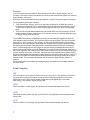
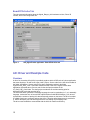
Self-Test
A Self-Test application named SR2_Analog_SelfTest is provided to test the SR2_Analog_16
board. This application can only work if the Signal_Ranger_mk2 board is functional. If any doubt
exists about the functionality of the Signal_Ranger_mk2, the user should first test it using the
SR2_SelfTest application.
The front-panel of the SR2_Analog_SelfTest application is shown below:
2
Figure 1:
SR2_Analog_Self_Test application
To run the application, simply click on the arrow at the top left of the window.
The application loads the FPGA logic, and then performs the following tests:
• Enumerates the number of AICs in each chain
• Tests the offset and noise of the AICs
• Tests the input/output (analog loopback) transfer function of the AICs, as well as their
distortion.
The transfer function and distortion tests are performed using the AIC’s analog loopback mode.
Therefore they do not test the output operational amplifier, or the connectors. However, the test
signal is still output on the connectors.
The transfer function and distortion tests are performed using a full-amplitude white signal. This is
likely to make a lot of noise if the outputs are connected to other equipment, such as a poweramplifier and speaker.
Indicators:
Test_Results: This array indicates the result of the following test for each channel. Channel 0 is
at the top, channel 15 is at the bottom.
- Off_OK
Indicates that the input offset is within +-50 mV. Note: the AIC is in
internal loopback during this test, so this is also indicative of the output offset.
- Noise_OK
Indicates that the noise is within 100 µVrms.
- Dist_OK
Indicates that the signal to (noise+distortion) ratio is at least 50 dB
- Trans_OK
Indicates that the input/output (loopback) transfer function is within +-1
dB of a reference transfer function. This test is only conducted on 90% of the bandwidth,
because errors of more than 2 dB in the transition band are not unusual.
• Amplitude (dB): Plots the input/output transfer functions for each AIC. The upper plot is a
zoom on the band-pass part of the plot.
• Progress:
Indicates the progress of the distortion and transfer function tests.
3
FPGA and DSP Setup
FPGA Configuration
Before attempting to manage the AICs, the FPGA should be configured with the
SR2_Analog_16.rbt logic. As discussed above, this configuration may be placed in Flash so that
it is loaded into the FPGA at power-up. Alternately, the configuration may be loaded dynamically
from the PC application, or directly from the DSP code, before the functions of the AIC DSP driver
are invoked. The example code uses dynamic loading. Therefore it does not rely on the state of
the FPGA immediately after power-up.
Some users may need to place additional logic in the FPGA. If this is considered, the minimum
requirements on the FPGA logic to properly support the provided AIC DSP driver are given
below:
•
•
•
•
There must be an AIC_Control register at byte address C00022H in the FPGA. The two lower
bits of this register must control the AIC_PwrDwn and AIC_Reset output lines, as described
in SR2_Analog_FPGA_Logic.pdf.
A DSP clock output must be used to generate the AIC Master Clock signal. The only
constraint is that the AIC Master Clock signal must be lower than 100MHz, and must be
output on pin 11 of the FPGA to be properly routed to the AICs (see factory-default FPGA
project pinout). In the factory default configuration the DSP CLKOut output is used to
generate a 150MHz signal on the FPGA pin 52. This signal is divided by 2 in the FPGA and
routed to the FPGA pin 11 to generate a 75MHz clock signal to the AIC Master Clock inputs.
In addition to using the DSP ClkOut output to generate the AIC Master Clock signal, the user
also has the options of using either the TIM0 or TIM1 DSP outputs. These alternate DSP
clock outputs are routed to pins 128 and 127 of the FPGA respectively.
Both AIC_PwrDwn and AIC_Reset FPGA outputs must be synchronized to the AIC_Clk_Out
FPGA output as explained in SR2_Analog_FPGA_Logic.pdf. Although it is a good start, it is
not sufficient to copy the AIC-management part of the logic from the provided Xilinx ISE
project. The timings outlined in SR2_Analog_FPGA_Logic.pdf must be verified.
The FPGA pinout for AIC_Clk_Out, AIC_PwrDwn and AIC_Reset must be maintained, since
they are tied to the layout of the SR2_Analog_16 board.
DSP Timer Configuration
In the factory-default configuration, the AIC_Clk_Out signal provided by the FPGA to the AIC
Master Clock inputs comes from the DSP’s CLKOut output. The Power-Up Kernel and HostDownload Kernel both configure the CLKOut output for a 150MHz output signal. If the CLKOut
output configuration is not changed by user DSP code, this provides a 75MHz AIC_Clk_Out
signal to the AIC Master Clock inputs immediately after FPGA configuration.
4
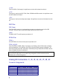
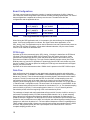
Hardware description
Connector map
Figure 2
Legend:
1
2
3
Analog connectors J1, J2, J3, J4, J6, J7, J8 and J9
Expansion connector J5
Signal_Ranger_mk2 connector J10
Expansion connector J5
3 6 9
2 5 8
1 4 7
No
1
4
7
10
13
16
19
22
25
28
31
34
5
...
Function
+5V
+1.8V
+1.26V
-3.3V
NC
NC
NC
NC
NC
NC
UART_Rx
NC
No
2
5
8
11
14
17
20
23
26
29
32
35
Function
Gnd
Gnd
Gnd
Gnd
Gnd
Gnd
Gnd
Gnd
Gnd
Gnd
Gnd
Gnd
No
3
6
9
12
15
18
21
24
27
30
33
36
Function
+2.5V
+1.2V
+3.3V
DSP_Reset
NC
NC
NC
NC
NC
NC
UART_Tx
Presence
37
40
43
46
49
52
55
58
61
64
67
70
73
76
79
82
85
88
91
94
97
100
103
106
109
112
115
118
121
124
127
130
Table 1:
FPGA_17
FPGA_14
FPGA_12
FPGA_10
FPGA_7
FPGA_5
FPGA_2
FPGA_141
FPGA_137
FPGA_68
FPGA_70
FPGA_74
FPGA_77
FPGA_79
FPGA_82
FPGA_84
FPGA_86
FPGA_89
FPGA_92
FPGA_95
FPGA_97
FPGA_99
FPGA_102
FPGA_104
FPGA_107
FPGA_112
FPGA_116
FPGA_119
FPGA_123
FPGA_125
FPGA_130
FPGA_132
38
41
44
47
50
53
56
59
62
65
68
71
74
77
80
83
86
89
92
95
98
101
104
107
110
113
116
119
122
125
128
131
Gnd
Gnd
Gnd
Gnd
Gnd
Gnd
Gnd
Gnd
Gnd
Gnd
Gnd
Gnd
Gnd
Gnd
Gnd
Gnd
Gnd
Gnd
Gnd
Gnd
Gnd
Gnd
Gnd
Gnd
Gnd
Gnd
Gnd
Gnd
Gnd
Gnd
Gnd
Gnd
39
42
45
48
51
54
57
60
63
66
69
72
75
78
81
84
87
90
93
96
99
102
105
108
111
114
117
120
123
126
129
132
NC
NC
NC
FPGA_8
FPGA_6
FPGA_4
FPGA_1
FPGA_140
FPGA_135
FPGA_69
FPGA_73
FPGA_76
FPGA_78
FPGA_80
FPGA_83
FPGA_85
FPGA_87
FPGA_90
FPGA_93
FPGA_96
FPGA_98
FPGA_100
FPGA_103
FPGA_105
FPGA_108
FPGA_113
FPGA_118
FPGA_122
FPGA_124
FPGA_129
FPGA_131
FPGA_HS_EN
Pinout of connector J5
Differences With Signal_Ranger_mk2 J4 Expansion Connector
Expansion connector J5 on SR2_Analog_16 is laid-out almost identically to
Signal_Ranger_mk2’s J4 connector. The differences are outlined below:
McBSP Signals
McBSP signals for both McBSP0 and McBSP1 are not provided on expansion connector J5. They
are used to manage the AICs and are therefore not available for general use anymore.
FPGA_15, FPGA_13, FPGA_11
FPGA IO bits FPGA_11, FPGA_13, FPGA_15 are not provided on J5 pin 45, 42 and 39. They are
used to manage the AICs and are therefore not available for general use anymore.
6
Presence
A new Presence input is provided on J5 pin 36 that did not exist on Signal_Ranger_mk2 J4
connector. This input is used to activate the bus switches that isolate all the signals of J5 from the
Signal_Ranger_mk2 board.
All the pins of J5 are isolated through the bus switches, except for the power-supply connections.
The bus switches provide two functions:
• They isolate Signal_Ranger_mk2 from a user board connected on J5 when one board is
powered but not the other. This is essential because in the absence of the switches, drivers
on one board could be driving un-powered input stages on the other, which could damage
them.
• They provide level translation between the user-board, which can drive levels up to 5V and
inputs on Signal_Ranger_mk2 that are not 5V-tolerant. In short, the switches make the inputs
on Signal_Ranger_mk2 5V-tolerant.
To provide the first function, the switches should only be activated (low-impedance) when the
user daughter board is powered. The Presence input serves this purpose. This input is normally
pulled-up by a 10 kΩ resistor on SR2_Analog_16. The input should be pulled low by an opendrain driver on the user’s daughter board when the daughter board is properly powered. Pulling
Presence low when the user’s daughter board is not properly powered (before it is powered or
after it is un-powered) exposes input stages on the user’s board to damage inflicted by FPGA
pins that may be configured as outputs. Depending on how the FPGA is configured at the time it
may not be a problem. For instance if the FPGA is not configured, its IOs are configured as inputs
and will not drive any current. In this case, Presence may be permanently tied to ground. Pulling
Presence low when the user’s daughter board is properly powered but Signal_Ranger_mk2 is not
DOES NOT EXPOSE the FPGA inputs to damage that may be inflicted by drivers on the user’s
daughter board. This is because the switches are off whenever Signal_Ranger_mk2 is unpowered.
The second function is provided automatically whenever the switches are activated (whenever
Presence is low).
Power Supplies
+5V
This is the same +5V line that is brought to the power connector J2. The maximum current that
may be drawn from this pin is 500mA. It may be further limited by the capacity of the powersupply that is used. This is the only power-supply that may be tapped by the user when
SR2_Analog_16 is mated to Signal_Ranger_mk2.
+2.5V
This is the FPGA’s Vccaux supply. No significant current should be drawn from this pin.
+1.8V
This supply is used to power the logic core of the AICs. No significant current should be drawn
from this pin.
+1.2V
This is the FPGA’s Vccint supply. No significant current should be drawn from this pin.
7
+1.26V
This is the DSP’s CVdd supply. No significant current should be drawn from this pin.
+3.3V
This supply is used by the DSP, FPGA, Flash, SDRAM and USB controller. No significant current
should be drawn from this pin.
-3.3V
This supply is used by the analog output stages. No significant current should be drawn from this
pin.
DSP Pins
DSP_Reset
This is the DSP’s reset pin. It is activated (low) at power-up, and under control of the USB
controller. It may be used to reset external logic whenever the DSP is reset.
UART
The DSP’s UART Tx and Rx pins are provided on J5.
FPGA Pins
FPGA_i
All of the FPGA’s free I/Os and clock pins are provided on J5.
FPGA_HS_EN
This is the FPGA’s HSWAP_EN pin. If pulled-up or left floating, all the FPGA’s I/Os are floating
during configuration. If it is pulled low, the FPGA’s I/Os are pulled-up during configuration. The
state of the FPGA’s I/Os after configuration is defined by the logic loaded into the FPGA, and the
state of HSWAP_EN has no bearing on it.
Note: FPGA_HS_EN is passed to expansion connector J5 through the bus switch. So in order
for the FPGA to see this pin in a low state during configuration, the bus switches must be
activated prior to FPGA configuration.
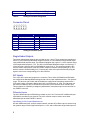
Analog IO Connectors J1, J2, J3, J4, J6, J7, J8, J9
Connector Assignments
Connector No
J1
J2
J3
J4
J6
J7
8
McBSP/CODEC_Addresses
McBSP_0 / CODEC_0 & CODEC_1 (Master)
McBSP_0 / CODEC_2 & CODEC_3
McBSP_0 / CODEC_4 & CODEC_5
McBSP_0 / CODEC_6 & CODEC_7
McBSP_1 / CODEC_0 & CODEC_1 (Master)
McBSP_1 / CODEC_2 & CODEC_3
J8
J9
McBSP_1 / CODEC_4 & CODEC_5
McBSP_1 / CODEC_6 & CODEC_7
Table 2:
Analog I/O connector assignment
Connector Pinout
2
4
6
8
10 12 14
1
3
5
7
9
No
1
3
5
7
9
11
13
11 13
Function
AIC_Out_2
Gnd
AIC_InP2
AIC_InM2
Gnd
InP4/InM4 (Mic_In)
+Vbias
Table 3:
No
2
4
6
8
10
12
14
Function
AIC_Out_3
Gnd
AIC_InP3
AIC_InM3
Gnd
InP1/InM1 (Mic_In)
+Vbias
Analog I/O connector pinout
Single-Ended Outputs
Two single-ended output channels are provided on pins 1 and 2. These outputs are transformed
from the 1.35V-referenced differential outputs of the AIC to a 0V-referenced single-ended output
using a differential amplifier stage. The differential amplifier has a gain of 1, so the dynamic range
of the single-ended outputs is +-2V. The AIC’s OutP2/OutM2 differential output is routed to pin 1
of the connector, while the AIC’s OutP3/OutM3 is routed to pin 2. The cross-bar inside the AIC
must be used to select which of the two CODEC outputs is routed to OutP2/OutM2 (pin1), and
which is routed to OutP3/OutM3 (pin 2). Choosing any other AIC output will effectively bring the
signal to zero on the corresponding pin on the connector.
AIC Inputs
Four of the AIC’s inputs are brought to the connector. Two of them (InP2/InM2 and InP3/InM3)
are configured as standard differential inputs with a 85 kΩ input impedance and a +-10V dynamic
range. The other two (InP1/InM1 and InP4/InM4) are configured as microphone inputs with a +2V dynamic range, microphone biasing and a low cut-off frequency of 16Hz. The user must use
the cross-bar inside the AIC to choose which connector input is routed to which CODEC input.
This provides a lot of flexibility to assign any differential or microphone input on the connector to
any CODEC in the AIC.
Differential Inputs
The AIC’s differential input InP2/InM2 is provided on pins 5 and 7 and the AIC’s differential input
InP3/InM3 is provided on pins 6 and 8. The AIC’s cross-bar must be used to route either
differential input to either CODEC in the AIC.
Input Biasing for DC-Coupled Measurements
On each differential inputs, a simple resistor network, and the AIC’s VBias output is used to bring
the dynamic range of each single-ended input to +-10V, and to offset each single-ended input so
9
that it is 0V-referenced at the connector level, rather than 1.35V-referenced - as it is at the AIC
level. For this resistor network to provide its function two conditions must be met:
• Each single-ended input of the differential pair (for instance pin 5 and pin7) must be driven by
a 0V-referenced low-impedance driver.
• The AIC must be set so that its VBias output is 2.35V, rather than 1.35V.
If an input of the differential pair is left floating, rather than driven at low-impedance, the static
voltage on the corresponding input of the AIC is 1.5V. Since each input of the AIC’s differential
pair is 1.35V-referenced, this 1.5V voltage is equivalent to a 150mV static offset on the AIC’s
input. If both inputs of the differential pair are left floating or driven at high impedance, the same
offset is applied to both inputs of the differential pair and it cancels out. However, in any case, this
static offset reduces the dynamic range of each single-ended input of the differential pair, thereby
lowering the saturation threshold of the AIC’s differential input stage.
If a single-ended source is used to drive the differential pair, simply connect it to either the InP or
InM input, and connect the other input to ground. Add 6dB to the input gain to compensate for the
absence of the differential signal.
Input Biasing for AC-Coupled Measurements
If the inputs of the differential pair are driven through an AC-coupling (a capacitor), then the AIC’s
VBias output should be set to 1.35V, rather than 2.35V. Otherwise a static offset equivalent to
150mV is applied to each input of the differential pair, reducing its dynamic range
correspondingly.
Note: The VBias setting for each AIC is common to both CODECs of the AIC, therefore the
user must choose either AC-coupling (VBias = 1.35V) or DC-coupling (VBias = 2.35V) for both
channels of the AIC.
Microphone Inputs
An electret microphone input can be selected as the input of either CODEC of the AIC. For this,
the electret microphone should be connected between pins 9 and 11 (for InP1/InM1), with the
positive on pin 11, and/or between pins 10 and 12 (for InP4/InM4), with the positive on pin 12.
The AIC’s cross-bar must be used to select which CODEC input is routed to InP1/InM1 (pins 9
and 11), and which is routed to InP4/InM4 (pins 10 and 12). The AIC should be set so that its
Vbias is 2.35V to properly bias most electret microphones.
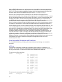
Software Description
Signal Tracker Demo Application
The Signal Tracker application has been designed to allow the test and evaluation of the analog
input/output channels. The application allows the user to send test signals to a selected channel
output, and monitor the sampled signal on a selected input. Inputs are displayed both in terms of
time signals, as well as instantaneous or averaged energy spectra. Averaged energy spectra are
useful to evaluate the input noise. The front-panel of the application is divided into several tabs,
one for each function group.
10
Figure 3:
SR2_SignalTracker application – Time Signal tab
To start the application, simply click on the white arrow at the top-left of the window.
The application sends blocks of samples of the selected length and waveform to the selected
output, and records blocks of samples of the same length on the selected input. The recorded
input samples are synchronous to the output samples.
Time Signal Tab
Time Indicator
The time-signal tab presents a time plot of the signal sampled on the selected input. The
amplitude scale takes into account the gain of the analog chain and PGA gain, so that the signal
amplitude is represented in Volts at the connector.
AC estimate (Vrms) Indicator
This indicator presents the RMS value of the input signal (any DC offset is removed before RMS
calculation), as well as the average DC value.
AC estimate (Vrms) Indicator
This indicator presents the average DC value of the time signal.
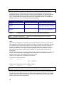
Sxx Tab
Spectrum Indicator
The Spectrum indicator presents the instantaneous or averaged power spectrum of the input
sampled block.
11
Figure 4:
SR2_SignalTracker application – Sxx tab
The vertical scale is in dB. A value of 0 dB represents an amplitude of 1Vrms.
Average Control
To average the power-spectrum, simply place the Average control in the ON position.
Reset Average Button
The Reset Average button resets the average.
Time Window selector
An optional window can be chosen from the Time-Window list.
Graph and Zoom Controls
Graph controls can be used to change the zoom factor. By default the plot is auto-scaled in X and
Y, which is indicated by the closed locks beside each scale name. To disable auto-scale, simply
press the lock button.
Acquisition Set-Up Tab
The Acquisition Set-Up tab presents the various controls for the acquisition set-up.
12
Figure 5:
SR2_SignalTracker application – Acquisition Set-Up tab
Signal Output Control
The Signal output control selects a type of waveform from a list of predefined waveforms. The No
Output selection sends zero samples to the output.
Block Size Control
The Block size control sets the number of samples that are sent to the output, and synchronously
recorded from the input.
Amplitude Control
The Amplitude control adjusts the amplitude of the output waveform. The output samples are
calculated according to the selected amplitude, as well as the selected output gain (PGA).
Frequency Control
The Frequency control is only used for periodic waveforms. It adjusts the fundamental frequency
of the waveform.
Input Codec Control
The Input Codec control selects the input channel between 0 and 15.
Output Codec Control
The Output Codec selects the output channel between 0 and 15.
Offset Compensation Control
The Offset Compensation button performs an offset compensation. This procedure reads a block
of input samples from the selected input while sending zero samples. The average of the
13
recorded samples is then subtracted from the input samples. Therefore, if any offset is present on
the selected input, it is brought to zero. The average is displayed in the Offset(I16) indicator. This
indicator is scaled in bits. The offset compensation is software.
Offset(I16) Control
The Offset(I16) indicator can also act as a control. Simply changing the content of this field
imposes a software offset to the recorded input samples.
AIC Set-Up Tab
The AIC Set-Up tab presents the various controls for the acquisition set-up.
Figure 6:
SR2_SignalTracker application – AIC Set-Up tab
AIC_Setup_Array Control
This array includes a setup field for each AIC chip (not each channel). By default the field for AIC
0 is shown. To access other AICs (0 to 7), simply change the index number I the upper left corner
of the field. The field includes a setup for the bias voltage (which is common to both channels of
the AIC), as well as a set of controls for each channel (A or B).
Global Parameters Control
This field includes all the adjustments that are common to all the AICs. The Fs(requested) field
contains the requested sampling frequency in Hz. The application adjusts the various AIC
counters to get a real sampling frequency as close as possible to the request. It automatically
takes into account the various limitations on the counter values.
Fs(real) indicator
This field indicates the real sampling frequency that has been achieved, given the finite resolution
of the AIC counters, as well as the various limitations on the counter values.
14
Board/FPGA infos Tab
This tab presents information about the Signal_Ranger_mk2 hardware revision, Driver ID
number, and FPGA configuration file.
Figure 7:
SR2_SignalTracker application –Board/FPGA infos tab
AIC Driver and Example Code
Overview
A driver for the analog I/Os (AICs) is provided, together with the DSP code of a demo application
that uses this driver, as well as an empty “shell” project. Source code for the AIC driver resides in
the folder AIC24Driver. Source code for the demo application resides in the folder
SignalTracker_DSP_Code. This folder contains the DSP code of the SignalTracker demo
application discussed above. Source code for the shell project resides in the
IO_Shell_DSP_Code folder. The shell project constitutes an excellent starting point for
developing DSP code that uses the AICs.
The driver has been optimized in assembly language, but can be used either in C, or in assembly
language. It takes the form of several DSP object libraries CodeDSPAIC24Driver_ii.lib, where ii
represents the number of analog I/Os that are actually present on the board. The driver contains
C-callable functions to configure and use the AICs. A function called dataprocess is provided in
C, where developers can conveniently place their own analog I/O processing code.
The driver uses the DMA to communicate with the AICs for maximum efficiency.
15
Board Configurations
The most common board configuration contains 16 analog inputs/outputs (8 AICs). However,
there exist other board configurations with reduced numbers of analog inputs/outputs. For each of
these configurations a separate driver library must be used. The table below lists the
configurations and the applicable driver:
Number of I/Os
16
8
4
Table 4:
Channel Numbers
0 to 7 (McBSP0)
8 to 15 (McBSP1)
0 to 3 (McBSP0)
8 to 11 (McBSP1)
0 to 1 (McBSP0)
8 to 9 (McBSP1)
Configuration
4 AICs (8 channels)
on each McBSP
2 AICs (4 channels)
on each McBSP
1 AICs (2 channels)
on each McBSP
Driver Library
CodeDSPAIC24Driver_16.lib
CodeDSPAIC24Driver_8.lib
CodeDSPAIC24Driver_4.lib
List of supported board configurations and drivers
When linking the DSP application code, it is important to link with the library for the applicable
board. If the board configuration is unknown, the SignalTracker demo application, or the
SR2_Analog_Self_Test application may be used to determine how many channels are present on
the board. For the sake of simplicity, except when indicated otherwise, only the most common
case of 16 I/O channels is discussed here.
FPGA Logic
Operation of the driver assumes that the SR2_Analog_16.rbt logic is loaded into the FPGA and
functional. This logic directs the DSP CLKOut output to the AIC master clock inputs. It also
generates and synchronizes the AICs reset and power-down inputs to the master-clock. The
driver does not load this FPGA logic. The logic must be loaded by another means (from Flash
ROM at power-up, from the PC application or dynamically from the DSP code, before any driver
function is called). The various options for loading the FPGA logic are documented in the Signal
Ranger_mk2 user’s manual.
Operation of the driver also assumes that a 75MHz clock is present on the DSP CLKOut output.
Data Flow
After configuration, the 8 channels in each bank begin exchanging samples and configuration
data to/from the DSP, via McBSP0 and McBSP1. Each McBSP supports a bank of 8 channels (1
Master and 7 slaves). These 8 channels sample the analog signals, and transmit/receive data in
sequence. The AICs communicate with the DSP in turbo mode, so that sampling times and
transmission period for each of the eight channels in a bank occur as fast as possible at the
beginning of each sampling period. The input/output transmission time lasts 3.41 µs per channel
(1 data word and 1 configuration word). The worst case is for 8 channels on each McBSP. In this
case the transmission period for all the channels in a bank takes 27.31 µs. The shortest sampling
period is 38.46 µs (26 kHz). For this sampling period, there is 11.15 µs of inactivity after the
transmission period, before the beginning of the next transmission period.
The exchange of sample and configuration data to/from each AIC, from/to a buffer in memory, is
performed in the background by four DMA channels (DMA channels 0 to 3). At each sampling
period, after all AIC sample and configuration data has been exchanged, the DMA channel 0
(DMAC0) interrupt is triggered. This interrupt service routine re-buffers the input and output data
into/from a user-accessible structure IOBuf, and calls the user-defined signal processing function
dataprocess, which can be written in C. The user-defined dataprocess function is packaged as a
TRAP (software interrupt #30). Dataprocess normally retrieves the input samples from the IOBuf
structure, and prepares (writes) the next output samples to the IOBuf structure. It has one
complete sampling period to do so.
16
After the DMAC0 flag goes to one, the interrupt must not be held for a long time, especially at
high sampling periods, otherwise samples are lost. For 16 channels the transmission period lasts
for 27.31 µs, so at the maximum sampling frequency of 26 kHz (sampling period 38.46 µs), the
maximum latency time for the DMAC0 interrupt is 38.46 µs – 27.31 µs = 11.15 µs.
Since the AIC input/output data is re-buffered, the user-defined function dataprocess is
guaranteed that the data will not change until the triggering of the next DMAC0 interrupt. It means
that the user-defined dataprocess function can be executing for up to the complete length of the
sampling period (38.46 µs at the maximum 26 kHz sampling frequency). It must however be
completed before the next triggering of the DMAC0 interrupt, otherwise a sampling period will be
lost and the same output samples will be sent to the AICs for two periods in a row.
Since it is called as a trap from within the DMA interrupt service routine, the dataprocess function
is normally un-interruptible. It can be made interruptible however by resetting the INTM bit to 0.
At each sampling period, the DSP exchanges samples and configuration data with each AIC. The
user-accessible IOBuf structure contains output samples, as well as configuration words to be
sent to the AICs. Normally after configuration there is no need to send more configuration words
to the AIC channels. Therefore, the start_aic24 function that configures the AICs writes
configuration words initialized at zero in the configuration members of the IOBuf structure. The
user code that does not need to reconfigure the AICs dynamically must simply not write these
configuration members. If dynamic reconfiguration is required, the user DSP code must write the
proper configuration codes into the configuration member of the IOBuf structure in the
dataprocess function. It must not fail to write configuration codes initialized at zero at the next call
of the dataprocess function. Otherwise the dynamic reconfiguration codes will be sent
continuously to the AICs.
User-Accessible Structures and Functions
The CodeDSPAIC24Driver_ii.lib library defines and allocates the following user-accessible
structures:
aic24reg
This structure is designed to contain the configuration register values for a maximum of 16
channels. The structure should be initialized with the desired parameters before the execution of
the start_aic24 function. The structure is defined in the AIC24Driver.h header file.
The structure is defined as follows:
struct
aicreg_rec
{
int
pReg4_m[16];
int
pReg4_n[16];
int
Reg3A [16];
int
Reg3B [16];
int
Reg3C [16];
int
Reg4_m [16];
int
Reg4_n [16];
int
Reg5A [16];
int
Reg5B [16];
int
Reg5C [16];
int
Reg6A [16];
int
Reg6B [16];
int
Reg1
[16];
int
Reg2
[16];
};
The structure is reserved by the driver library as follows:
struct
aicreg_rec
aic24reg;
17
Note: The structure is reserved automatically as a consequence of including the driver library
with the user DSP code. There is no need for the user DSP code to reserve this structure.
The same structure is defined and used for all the board configurations. However, only the
configuration registers for the existing AIC channels must be initialized. The following table lists
the configuration registers that are used for each board configuration. The generic notation
“reg_x” is used intable 5 to represent any specific AIC configuration register. The arrangement
described in table 5 is true for all the AIC configuration registers.
Board Configuration
4 AICs (8 channels) on each
McBSP
2 AICs (4 channels) on each
McBSP
Total Number of Channels
16
Configuration Registers
reg_x[0] to reg_x[15]
8
reg_x [0] to reg_x [3] (McBSP0)
reg_x [8] to reg_x [11] (McBSP1)
1 AICs (2 channels) on each
McBSP
4
reg_x [0] to reg_x [1] (McBSP0)
reg_x [8] to reg_x [9] (McBSP1)
Table 5:
Configuration registers used as a function of the board configuration
Note: All symbols must have an “_” prefix when used from assembly code. For instance
aic24reg becomes _aic24reg in assembly.
iobuf
This structure is designed to contain the input and output samples to/from the AICs, as well as
the configuration words to be sent to the AICs in the case of a dynamic reconfiguration. The user
code reads the min[i] registers and writes the mout[i] registers at each call of the dataprocess
function. Normally there is no need to dynamically reconfigure the AICs, so only the output
samples are updated in the mout[i] array. The configuration words are initialized to zero by the
start_aic24 function, and are normally never modified. This way they have no effect on the
configuration.
The user DSP code has one complete sampling period to execute the dataprocess function. If the
function is not completed within a sampling period input samples are overwritten by the new
samples, and the same output samples are sent to the AICs.
The structure is defined in the AIC24Driver.h header file.
The structure is defined as follows:
struct
iobuf_rec
{
int
min[32];
int
mout[32] ;
};
The structure is reserved by the driver library as follows:
struct
iobuf_rec
iobuf;
Note: The structure is reserved automatically as a consequence of including the driver library
with the user DSP code. There is no need for the user DSP code to reserve this structure.
The input and output registers contain the sample data first and the configuration data afterward.
The same structure is defined and used for all the board configurations. However, only the data
registers for the existing AIC channels must be used. The following table lists the data registers
that are used for each board configuration.
18
Board Configuration
4 AICs (8 channels) on
each McBSP
Total
Number of
Channels
16
2 AICs (4 channels) on
each McBSP
8
1 AICs (2 channels) on
each McBSP
4
Table 6:
Input/Output Buffer
min[0] to min[7]: input samples for channels 0 to 7
min[8] to min[15]: input configuration words for channels 0
to 7
min[16] to min[23]: input samples for channels 8 to 15
min[24] to min[31]: input configuration words for channels
8 to 15
mout[0] to mout[7]: output samples for channels 0 to 7
mout[8] to mout[15]: output configuration words for
channels 0 to 7
mout[16] to mout[23]: output samples for channels 8 to 15
mout[24] to mout[31]: output configuration words for
channels 8 to 15
min[0] to min[3]: input samples for channels 0 to 3
min[4] to min[7]: input configuration words for channels 0
to 3
min[8] to min[15]: not used
min[16] to min[19]: input samples for channels 8 to 11
min[20] to min[23]: input configuration words for channels
8 to 11
min[24] to min[31]: not used
mout[0] to mout[3]: output samples for channels 0 to 3
mout[4] to mout[7]: output configuration words for
channels 0 to 3
mout[8] to mout[15]: not used
mout[16] to mout[19]: output samples for channels 8 to 11
mout[20] to mout[23]: output configuration words for
channels 8 to 11
mout[24] to mout[31]: not used
min[0] to min[1]: input samples for channels 0 to 1
min[2] to min[3]: input configuration words for channels 0
to 1
min[4] to min[15]: not used
min[16] to min[17]: input samples for channels 8 to 9
min[18] to min[19]: input configuration words for channels
8 to 9
min[20] to min[31]: not used
mout[0] to mout[1]: output samples for channels 0 to 1
mout[2] to mout[3]: output configuration words for
channels 0 to 1
mout[4] to mout[15]: not used
mout[16] to mout[17]: output samples for channels 8 to 9
mout[18] to mout[19]: output configuration words for
channels 8 to 9
mout[20] to mout[31]: not used
IO registers used as a function of the board configuration
Note: All symbols must have an “_” prefix when used from assembly code. For instance iobuf
becomes _iobuf in assembly.
19
start_aic24
This function configures the AICs and starts the AIC conversion process. It has no arguments. It
uses the register configuration values found in the aic24reg structure and configures the AICs
accordingly. These values must be initialized prior to calling start_aic24. They set AIC parameters
such as sampling frequency, input and output gain…etc. according to the functions of the AIC
registers. After the execution of this function, the user-defined processing function called
dataprocess starts being triggered at each sampling period. The LabVIEW AIC interface library
includes a VI to generate the register contents automatically as a function of user-selected AIC
functions.
The function is defined in the AIC24Driver.h header file.
Note: All symbols must have an “_” prefix when used from assembly code. start_aic24 must be
written _start_aic24 in assembly.
stop_aic24
This function stops the AIC conversion process. After the execution of this function, the userdefined dataprocess function stops being triggered and all the AICs continuously output zero
samples.
The function is defined in the AIC24Driver.h header file.
Note: All symbols must have an “_” prefix when used from assembly code. stop_aic24 must be
written _stop_aic24 in assembly.
dataprocess
This function is declared by the AIC driver library, but must be provided by the user. It usually
contains the DSP code that reads the input samples from the iobuf structure, performs the signal
processing between the inputs and outputs and writes the ouput samples to the iobuf structure.
Note that the dataprocess function is actually a TRAP.
In assembly, this function must protect all registers that it uses, and must be terminated by a
RETI instruction. The dataprocess symbol must be declared using the .global directive.
In C, this function must be defined with the interrupt keyword.
Note: All symbols must have an “_” prefix when used from assembly code. dataprocess must
be written _dataprocess in assembly.
Used Resources
The AIC driver uses the following hardware resources:
• Both McBSP0 and McBSP1 are used by the driver.
• DMA channels 0 to 3 are used by the driver.
• The DMAC0 interrupt is used by the driver.
• TRAP #30 is used by the driver.
• The driver uses 1045 bytes for the code and 352 words for the data.
• The DSP CLKOut output is used to output the 75 MHz AIC master-clock.
Restrictions
When developing C or assembly code using the AIC driver, the following restrictions apply:
• The user-defined I/O processing function dataprocess must be present in the user code. If
the function is defined in C, it must be defined with the interrupt specifier. This way, the
compiler does a full context save when entering the function. If it is defined in assembly, all
DSP registers used within the function must be protected upon entry, and restored before
20
•
•
•
•
return. It must end with the RETI instruction. The dataprocess symbol must be defined using
the .global directive.
For the DMA to work properly, the sampling rate must be identical for all the AICs in both
banks.
All C-accessible symbols and labels defined in the CodeDSPAIC24Driver_ii.lib library must
have a “_” prefix when used in assembly language.
The entire code and data sections (including .bss section) of the CodeDSPAIC24Driver_ii.lib
library must be linked in the internal memory.
The Software interrupt #30 is used by the driver to call the dataprocess user function. The
vector for this software interrupt must be properly declared. See the SignalTracker demo
DSP code for an example of a correct vectors.asm.
Driver Lock-Up
Because the driver relies on the DMA for transfers of samples to and from the AICs, there are
situations that can lead to a lock-up. The DARAM can only support 2 accesses per cycle, for
which the CPU always has priority against DMA and HPI accesses. Some rare sequences of
instructions, when executed in a tight loop require those two DARAM accesses per cycle, thereby
completely denying access of the DARAM block from which the code is executing to the DMA.
This condition occurs only when the code is executing from the same DARAM block where the
DMA buffer resides. Under these conditions the DMA transfers never complete. Therefore the
interrupt #30 is never triggered and the dataprocess user function is never called. This situation
may be accompanied by a USB lock-up if the code executes from the first DARAM block,
because the HPI uses the DMA for transfers and is subject to the same priority rules (see
Signal_Ranger_mk2_UserManual.pdf).
There are several workarounds that can be applied:
• The DMA buffer may be moved to another DARAM block from the block containing the
offending code loop.
• The offending code loop may be modified to avoid requiring two accesses per cycle. A simple
fix is usually to insert NOP instructions in the loop. The situation is very rare so most code
reorganizations will usually fix the problem.
AIC LabVIEW library
A LabVIEW library is provided to manage the AICs. This library relies on various executable DSP
codes to provide the functions. The DSP codes are loaded as required by the library functions.
SR2_DetectionOfNumberofAIC24.vi
This VI detects the number of AICs that are present in each McBSP bank. The VI relies on the
SR2_Analog_16.rbt FPGA logic, as well as the SR2_AIC24Detection.out DSP code. Both are
dynamically loaded by the VI. Any previously running DSP code is aborted. Any previously
implemented FPGA logic is erased.
Controls:
• BoardRef:
This is a number pointing to the entry corresponding to the board in the
Global Board Information Structure. It is created by SR2_Base_Open_Next_Avail_Board.vi
• Progress
This is a reference that may be connected to a progress bar. The
progress bar varies during the execution of the VI between 0 (process just started) and 1
(process completed).
21
•
Error in:
LabView instrument-style error cluster. Contains error number and
description of the previously running Vi.
Indicators:
• DupBoardRef:
This is a number pointing to the entry corresponding to the board in the
Global Board Information Structure. It is created by SR2_Base_Open_Next_Avail_Board.vi
Use this output to propagate the reference number to other Vis.
• Error out:
LabView instrument-style error cluster. Contains error number and
description.
• FPGAInfo(out)
Cluster of information specific to the loaded FPGA logic.
• Number Of AIC24(McBSP0)
Number of AICs discovered in the McBSP0 chain.
• Number Of AIC24(McBSP1)
Number of AICs discovered in the McBSP1 chain.
• Channel(ON/OFF)
This is a 16-element Boolean array. Each element is
TRUE when the corresponding AIC is present, and FALSE when the AIC is absent.
SR2_Generate_AIC24_Registers.vi
This VI generates the configuration registers for user-specified AIC functions and optionally loads
them into the aic24reg structure. When Load Register is false, this VI does not require any DSP
code or FPGA logic. The register contents are provided to the user for information. When Load
Register is true, the SR2_Analog_16.rbt FPGA logic must be loaded in the FPGA, and a DSP
code using the CodeDSPAIC24Driver_ii.lib must be loaded in DSP memory. The DSP code does
not need to be running when the aic24reg structure is initialized. Any DSP code implementing the
CodeDSPAIC24Driver_ii.lib is compatible with the VI.
Controls:
• BoardRef:
This is a number pointing to the entry corresponding to the board in the
Global Board Information Structure. It is created by SR2_Base_Open_Next_Avail_Board.vi
• Error in:
LabView instrument-style error cluster. Contains error number and
description of the previously running Vi.
• P
This control sets the value of the P divisor in the AIC registers. Because
of a silicon bug on this AIC, this control should be left unconnected, or explicitly set to 8. AIC
manufactured after July 2005 do not have the bug.
• Global Parameters
This is a cluster that contains all the parameters that act on all
the AICs on the board.
• AIC24 set-up array
This array of clusters contains all the parameters that are specific
to each AIC and/or each channel. This array must always contain 8 elements (one per AIC),
even for a board that has less than 8 AICs. The elements are always numbered 0 to 3 for the
McBSP0 bank, and 4 to 7 for the McBSP1 bank. Therefore for a board that has only 2 AICs in
each bank, the relevant set-up elements would be 0 and 1, and 4 and 5.
• Load Registers
This Boolean selects whether or not the AIC register contents are
loaded into the aic24reg configuration structure. Note that loading the aic24reg structure by
itself does not reconfigure the AICs. To reconfigure the AICs, the start_aic24 DSP function
should be called after the load. For the load to proceed, the DSP memory should be loaded
with a code that implements the CodeDSPAIC24Driver_ii.lib. This DSP code does not need
to be running at the time of the load.
22
•
MCLK
Adjusts the master clock frequency. This frequency is 75 MHz by
default. This is the default frequency generated by the DSP ClkOut output, and that is
required to drive the AICs. This control should usually be left unconnected. However, if the
user needs to drive the AICs using a different MClk frequency (for instance by using the
DCMs in the FPGA), then this input can be used to support this other frequency.
Indicators:
• DupBoardRef:
This is a number pointing to the entry corresponding to the board in the
Global Board Information Structure. It is created by SR2_Base_Open_Next_Avail_Board.vi
Use this output to propagate the reference number to other Vis.
• Error out:
LabView instrument-style error cluster. Contains error number and
description.
• Fs(out)
This is the exact sampling frequency that is achievable given the finite
precision counters in the AICs, as well as various constraints on these counters. The VI tries
to find the register configuration that will produce the sampling frequency closest to what the
user requests.
• Registers
This array contains all the register contents to achieve the requested
configuration. If Load Registers is TRUE, these register contents are automatically loaded
into the aic24reg structure in DSP memory.
23