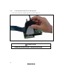
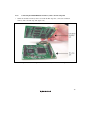
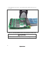
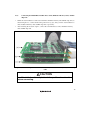
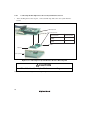
1
To our customers,
Old Company Name in Catalogs and Other Documents
On April 1st, 2010, NEC Electronics Corporation merged with Renesas Technology
Corporation, and Renesas Electronics Corporation took over all the business of both
companies. Therefore, although the old company name remains in this document, it is a valid
Renesas Electronics document. We appreciate your understanding.
Renesas Electronics website: http://www.renesas.com
April 1st, 2010
Renesas Electronics Corporation
Issued by: Renesas Electronics Corporation (http://www.renesas.com)
Send any inquiries to http://www.renesas.com/inquiry.
Notice
1.
2.
3.
4.
5.
6.
7.
All information included in this document is current as of the date this document is issued. Such information, however, is
subject to change without any prior notice. Before purchasing or using any Renesas Electronics products listed herein, please
confirm the latest product information with a Renesas Electronics sales office. Also, please pay regular and careful attention to
additional and different information to be disclosed by Renesas Electronics such as that disclosed through our website.
Renesas Electronics does not assume any liability for infringement of patents, copyrights, or other intellectual property rights
of third parties by or arising from the use of Renesas Electronics products or technical information described in this document.
No license, express, implied or otherwise, is granted hereby under any patents, copyrights or other intellectual property rights
of Renesas Electronics or others.
You should not alter, modify, copy, or otherwise misappropriate any Renesas Electronics product, whether in whole or in part.
Descriptions of circuits, software and other related information in this document are provided only to illustrate the operation of
semiconductor products and application examples. You are fully responsible for the incorporation of these circuits, software,
and information in the design of your equipment. Renesas Electronics assumes no responsibility for any losses incurred by
you or third parties arising from the use of these circuits, software, or information.
When exporting the products or technology described in this document, you should comply with the applicable export control
laws and regulations and follow the procedures required by such laws and regulations. You should not use Renesas
Electronics products or the technology described in this document for any purpose relating to military applications or use by
the military, including but not limited to the development of weapons of mass destruction. Renesas Electronics products and
technology may not be used for or incorporated into any products or systems whose manufacture, use, or sale is prohibited
under any applicable domestic or foreign laws or regulations.
Renesas Electronics has used reasonable care in preparing the information included in this document, but Renesas Electronics
does not warrant that such information is error free. Renesas Electronics assumes no liability whatsoever for any damages
incurred by you resulting from errors in or omissions from the information included herein.
Renesas Electronics products are classified according to the following three quality grades: “Standard”, “High Quality”, and
“Specific”. The recommended applications for each Renesas Electronics product depends on the product’s quality grade, as
indicated below. You must check the quality grade of each Renesas Electronics product before using it in a particular
application. You may not use any Renesas Electronics product for any application categorized as “Specific” without the prior
written consent of Renesas Electronics. Further, you may not use any Renesas Electronics product for any application for
which it is not intended without the prior written consent of Renesas Electronics. Renesas Electronics shall not be in any way
liable for any damages or losses incurred by you or third parties arising from the use of any Renesas Electronics product for an
application categorized as “Specific” or for which the product is not intended where you have failed to obtain the prior written
consent of Renesas Electronics. The quality grade of each Renesas Electronics product is “Standard” unless otherwise
expressly specified in a Renesas Electronics data sheets or data books, etc.
“Standard”:
8.
9.
10.
11.
12.
Computers; office equipment; communications equipment; test and measurement equipment; audio and visual
equipment; home electronic appliances; machine tools; personal electronic equipment; and industrial robots.
“High Quality”: Transportation equipment (automobiles, trains, ships, etc.); traffic control systems; anti-disaster systems; anticrime systems; safety equipment; and medical equipment not specifically designed for life support.
“Specific”:
Aircraft; aerospace equipment; submersible repeaters; nuclear reactor control systems; medical equipment or
systems for life support (e.g. artificial life support devices or systems), surgical implantations, or healthcare
intervention (e.g. excision, etc.), and any other applications or purposes that pose a direct threat to human life.
You should use the Renesas Electronics products described in this document within the range specified by Renesas Electronics,
especially with respect to the maximum rating, operating supply voltage range, movement power voltage range, heat radiation
characteristics, installation and other product characteristics. Renesas Electronics shall have no liability for malfunctions or
damages arising out of the use of Renesas Electronics products beyond such specified ranges.
Although Renesas Electronics endeavors to improve the quality and reliability of its products, semiconductor products have
specific characteristics such as the occurrence of failure at a certain rate and malfunctions under certain use conditions. Further,
Renesas Electronics products are not subject to radiation resistance design. Please be sure to implement safety measures to
guard them against the possibility of physical injury, and injury or damage caused by fire in the event of the failure of a
Renesas Electronics product, such as safety design for hardware and software including but not limited to redundancy, fire
control and malfunction prevention, appropriate treatment for aging degradation or any other appropriate measures. Because
the evaluation of microcomputer software alone is very difficult, please evaluate the safety of the final products or system
manufactured by you.
Please contact a Renesas Electronics sales office for details as to environmental matters such as the environmental
compatibility of each Renesas Electronics product. Please use Renesas Electronics products in compliance with all applicable
laws and regulations that regulate the inclusion or use of controlled substances, including without limitation, the EU RoHS
Directive. Renesas Electronics assumes no liability for damages or losses occurring as a result of your noncompliance with
applicable laws and regulations.
This document may not be reproduced or duplicated, in any form, in whole or in part, without prior written consent of Renesas
Electronics.
Please contact a Renesas Electronics sales office if you have any questions regarding the information contained in this
document or Renesas Electronics products, or if you have any other inquiries.
(Note 1) “Renesas Electronics” as used in this document means Renesas Electronics Corporation and also includes its majorityowned subsidiaries.
(Note 2) “Renesas Electronics product(s)” means any product developed or manufactured by or for Renesas Electronics.
User’s Manual
SH-2A, SH-2 E200F Emulator
Additional Document for User’s Manual
Supplementary Information on Using
the SH7206
Renesas Microcomputer
Development Environment
System
SuperH™ Family / SH7200 Series
E200F for SH7206 Group R0E572060EMU00E
Rev.9.00 2007.03
Notes regarding these materials
1. This document is provided for reference purposes only so that Renesas customers may select the appropriate
Renesas products for their use. Renesas neither makes warranties or representations with respect to the
accuracy or completeness of the information contained in this document nor grants any license to any
intellectual property rights or any other rights of Renesas or any third party with respect to the information in
this document.
2. Renesas shall have no liability for damages or infringement of any intellectual property or other rights arising
out of the use of any information in this document, including, but not limited to, product data, diagrams, charts,
programs, algorithms, and application circuit examples.
3. You should not use the products or the technology described in this document for the purpose of military
applications such as the development of weapons of mass destruction or for the purpose of any other military
use. When exporting the products or technology described herein, you should follow the applicable export
control laws and regulations, and procedures required by such laws and regulations.
4. All information included in this document such as product data, diagrams, charts, programs, algorithms, and
application circuit examples, is current as of the date this document is issued. Such information, however, is
subject to change without any prior notice. Before purchasing or using any Renesas products listed in this
document, please confirm the latest product information with a Renesas sales office. Also, please pay regular
and careful attention to additional and different information to be disclosed by Renesas such as that disclosed
through our website. (http://www.renesas.com )
5. Renesas has used reasonable care in compiling the information included in this document, but Renesas
assumes no liability whatsoever for any damages incurred as a result of errors or omissions in the information
included in this document.
6. When using or otherwise relying on the information in this document, you should evaluate the information in
light of the total system before deciding about the applicability of such information to the intended application.
Renesas makes no representations, warranties or guaranties regarding the suitability of its products for any
particular application and specifically disclaims any liability arising out of the application and use of the
information in this document or Renesas products.
7. With the exception of products specified by Renesas as suitable for automobile applications, Renesas
products are not designed, manufactured or tested for applications or otherwise in systems the failure or
malfunction of which may cause a direct threat to human life or create a risk of human injury or which require
especially high quality and reliability such as safety systems, or equipment or systems for transportation and
traffic, healthcare, combustion control, aerospace and aeronautics, nuclear power, or undersea communication
transmission. If you are considering the use of our products for such purposes, please contact a Renesas
sales office beforehand. Renesas shall have no liability for damages arising out of the uses set forth above.
8. Notwithstanding the preceding paragraph, you should not use Renesas products for the purposes listed below:
(1) artificial life support devices or systems
(2) surgical implantations
(3) healthcare intervention (e.g., excision, administration of medication, etc.)
(4) any other purposes that pose a direct threat to human life
Renesas shall have no liability for damages arising out of the uses set forth in the above and purchasers who
elect to use Renesas products in any of the foregoing applications shall indemnify and hold harmless Renesas
Technology Corp., its affiliated companies and their officers, directors, and employees against any and all
damages arising out of such applications.
9. You should use the products described herein within the range specified by Renesas, especially with respect
to the maximum rating, operating supply voltage range, movement power voltage range, heat radiation
characteristics, installation and other product characteristics. Renesas shall have no liability for malfunctions or
damages arising out of the use of Renesas products beyond such specified ranges.
10. Although Renesas endeavors to improve the quality and reliability of its products, IC products have specific
characteristics such as the occurrence of failure at a certain rate and malfunctions under certain use
conditions. Please be sure to implement safety measures to guard against the possibility of physical injury, and
injury or damage caused by fire in the event of the failure of a Renesas product, such as safety design for
hardware and software including but not limited to redundancy, fire control and malfunction prevention,
appropriate treatment for aging degradation or any other applicable measures. Among others, since the
evaluation of microcomputer software alone is very difficult, please evaluate the safety of the final products or
system manufactured by you.
11. In case Renesas products listed in this document are detached from the products to which the Renesas
products are attached or affixed, the risk of accident such as swallowing by infants and small children is very
high. You should implement safety measures so that Renesas products may not be easily detached from your
products. Renesas shall have no liability for damages arising out of such detachment.
12. This document may not be reproduced or duplicated, in any form, in whole or in part, without prior written
approval from Renesas.
13. Please contact a Renesas sales office if you have any questions regarding the information contained in this
document, Renesas semiconductor products, or if you have any other inquiries.
Contents
Section 1 System Configuration ........................................................................1
1.1
1.2
Components of the Emulator ............................................................................................ 1
System Configuration ....................................................................................................... 4
Section 2 Connecting the Emulator to the User System ....................................7
2.1
2.2
2.3
2.4
2.5
2.6
2.7
2.8
2.9
Connecting the Emulator to the User System ................................................................... 7
Connecting the Emulator to the User System by Using the EV-chip Unit........................ 7
2.2.1 Connecting the EV-chip Unit to the Emulator ..................................................... 7
2.2.2 Connecting the E200F External Bus Trace Unit to the EV-chip Unit ................. 10
2.2.3 Connecting the Probe Head to the EV-chip Unit ................................................. 12
2.2.4 Connecting the E200F Emulation Memory Unit to the EV-chip Unit................. 13
2.2.5 Connecting the E200F External Bus Trace Unit, Emulation Memory Unit,
and EV-chip Unit ................................................................................................. 15
2.2.6 Connecting the EV-chip Unit to the User System Interface Board...................... 16
Connecting the Emulator to the User System by Using the H-UDI Port Connector......... 17
Installing the H-UDI Port Connector on the User System ................................................ 18
Pin Assignments of the H-UDI Port Connector ................................................................ 18
Recommended Circuit between the H-UDI Port Connector and the MCU ...................... 20
2.6.1 Recommended Circuit (36-Pin Type) .................................................................. 20
Connecting the E200F External Bus Trace Unit with the User System ............................ 22
Installing the External Bus Trace Unit Connector ............................................................ 22
2.8.1 External Bus Trace Unit Connector Installed on the User System ...................... 22
2.8.2 Pin Assignments of the User System Connector.................................................. 22
2.8.3 Recommended Foot Pattern ................................................................................. 23
2.8.4 Restrictions on Component Installation ............................................................... 23
2.8.5 Pin Assignments of the External Bus Trace Unit Connector ............................... 24
2.8.6 Layout of the External Bus Trace Unit Connector............................................... 32
Connecting the External Bus Trace Unit to the User System ........................................... 34
2.9.1 Connecting the E200F External Bus Trace Unit to the Emulator Main Unit....... 34
2.9.2 Connecting the E200F External Bus Trace Unit to the User System................... 36
2.9.3 Connecting the E200F Emulation Memory Unit to the Emulator Main Unit ...... 37
2.9.4 Connecting the Emulation Memory Unit to the User System.............................. 39
2.9.5 Connecting the E200F External Bus Trace Unit, Emulation Memory Unit,
and User System .................................................................................................. 40
Section 3 Software Specifications when Using the SH7206 .............................43
i
3.1
3.2
Differences between the SH7206 and the Emulator ......................................................... 43
Specific Functions for the Emulator when Using the SH7206 ......................................... 51
3.2.1 Event Condition Functions .................................................................................. 51
3.2.2 Trace Functions ................................................................................................... 58
3.2.3 Notes on Using the JTAG (H-UDI) Clock (TCK) and AUD Clock (AUDCK) .. 70
3.2.4 Notes on Setting the [Breakpoint] Dialog Box .................................................... 70
3.2.5 Notes on Setting the [Event Condition] Dialog Box and
the BREAKCONDITION_ SET Command ........................................................ 71
3.2.6 Performance Measurement Function ................................................................... 71
Section 4 User System Interface Circuits ..........................................................77
4.1
4.2
ii
User System Interface Circuits ......................................................................................... 77
Delay Time for the User System Interface........................................................................ 81
Section 1 System Configuration
1.1
Components of the Emulator
The E200F emulator supports the SH7206. Table 1.1 lists the components of the emulator.
Table 1.1 Components of the Emulator
Classification Component
Hardware
Emulator main unit
AC adapter
Appearance
Quantity
1
Remarks
R0E0200F1EMU00:
Depth: 195.0 mm, Width: 130.0
mm,
Height: 45.0 mm, Mass: 490.0 g
Product numbers: 0001 to 0113
1
Input: 100 to 240 V
Output: 12 V 4.0 A
Depth: 120.0 mm, Width: 72.0 mm,
Height: 27.0 mm, Mass: 400.0 g
Product numbers: 0114 or later
1
Input: 100 to 240 V
Output: 12 V 3.0 A
Depth: 99.0 mm, Width: 62.0 mm,
Height: 26.0 mm, Mass: 270.0 g
AC cable
1
Length: 2000 mm
1
Table 1.1 Components of the Emulator (cont)
Classification Component
Hardware
(cont)
USB cable
External probe
Appearance
Quantity
Remarks
1
Length: 1500 mm, Mass: 50.6 g
Product numbers: 0001 to 0113
1
Length: 500 mm,
Pins 1 to 4: probe input pins,
T: trigger output pin,
G: GND pin
Product numbers: 0114 or after
1
Length: 500 mm,
Pins 1 to 4: probe input pins,
T: trigger output pin,
G: GND pin
Software
E200F emulator setup
1
R0E0200F1EMU00S,
program,
SH-2A, SH-2 E200F
R0E0200F1EMU00J,
Emulator User’s Manual,
R0E0200F1EMU00E,
and
Supplementary
R0E572060EMU00J, and
Information on Using the
R0E572060EMU00E
SH7206*
(provided on a CD-R)
Note: Additional document for the MCUs supported by the emulator is included. Check the target
MCU and refer to its additional document.
2
Table 1.2 Optional Components of the Emulator
Classification Component
Hardware
Appearance
Quantity
Remarks
External bus trace unit
1
R0E0200F1ETU00:
Depth: 90.0 mm, Width: 125.0 mm,
Height: 15.2 mm, Mass: 83 g
Emulation memory unit
(Memory capacity:
8 Mbytes or 16 Mbytes)
1
EV-chip unit
1
R0E0200F1MSR00 (8 Mbytes),
R0E0200F1MSR01 (16 Mbytes):
Depth: 90.0 mm, Width: 125.0 mm,
Height: 15.2 mm,
Mass: 81 g (R0E0200F1MSR00),
85 g (R0E0200F1MSR01)
Note that it is not possible to
connect these emulation memory
units at the same time.
R0E572060VKK00:
Depth: 110.0 mm, Width: 125.0
mm, Height: 15.2 mm, Mass: 110 g
Trace cable
1
R0E0200F0ACC00:
Length: 300 mm, Mass: 65 g
User system interface
board
1
R0E572060CFK00:
Depth: 60.0 mm, Width: 90.0 mm,
Height: 26.0 mm, Mass: 45 g
Expansion profiling unit
1
R0E0200F0EPU00:
Depth: 98.0 mm, Width: 115.0 mm,
Height: 15.2 mm, Mass: 52 g
3
1.2
System Configuration
Figure 1.1 shows an example of the emulator system configuration.
- When the EV-chip unit is not used:
Expansion profiling unit
High-performance
Embedded Workshop
USB 2.0/1.1
External bus
trace unit
E200F
User system
H-UDI and AUD
Trace cable
PC
- When the EV-chip unit is used:
Expansion profiling unit
Trace cable
External bus
trace unit
High-performance
Embedded Workshop
Emulation memory unit
USB 2.0/1.1
User system
interface board
EV-chip unit
IC socket
PC
E200F
Figure 1.1 System Configuration Using the Emulator
(1) System Configuration of the SH7206
Table 1.3 shows the system configuration supported by the SH7206.
4
User system
Table 1.3 System Configuration Supported by the SH7206 E200F
E200F Emulator
EV-chip Unit
External Bus
Emulation Memory Expansion
Trace Unit
Unit
Profiling Unit
User System
Trace Cable
Interface Board
R0E0200F1MSR00
R0E0200F1EMU00 R0E572110VKK00 R0E0200F1ETU00 R0E0200F1MSR01 R0E0200F0EPU00 R0E0200F0ACC00 R0E572110CFK00
System
Supported
Not supported
Not supported
Not supported
Not supported
Not supported
Not supported
Supported
Not supported
Supported
Not supported
Not supported
Supported
Not supported
Supported
Not supported
Supported
Supported
Not supported
Supported
Not supported
Supported
Not supported
Not supported
Supported
Not supported
Supported
Not supported
Supported
Supported
Not supported
Not supported
Not supported
Supported
Supported*2
Supported
Supported
Not supported
Supported
Not supported
Supported
Supported*2
Supported
Supported
Supported
Not supported
Not supported
Supported
Supported*2
Supported
Supported
Supported
Supported
Not supported
Supported
Supported*2
Supported
Not supported
Not supported
Not supported
Supported
Not supported
Not supported
Supported
Not supported
Supported
Not supported
Supported
Supported
Not supported
configu-ration
1*1
System
configu-ration
2*1
System
configu-ration
3*1
System
configu-ration
4*1
System
configu-ration
5
System
configu-ration
6
System
configu-ration
7
System
configu-ration
8
System
configu-ration
9*1
System
configu-ration
10*1
5
Table 1.3 System Configuration Supported by the SH7206 E200F (cont)
E200F Emulator
EV-chip Unit
External Bus
Emulation Memory Expansion
Trace Unit
Unit
Profiling Unit
User System
Trace Cable
Interface Board
R0E0200F1MSR00
R0E0200F1EMU00 R0E572110VKK00 R0E0200F1ETU00 R0E0200F1MSR01 R0E0200F0EPU00 R0E0200F0ACC00 R0E572110CFK00
System
Supported
Not supported
Supported
Supported
Supported
Supported
Not supported
Supported
Not supported
Not supported
Supported
Supported
Supported
Not supported
Supported
Supported
Not supported
Not supported
Supported
Supported
Supported*2
Supported
Supported
Not supported
Supported
Supported
Supported
Supported*2
Supported
Supported
Supported
Not supported
Supported
Supported
Supported*2
Supported
Supported
Supported
Supported
Supported
Supported
Supported*2
configuration 11*1
System
configuration 12*1
System
configuration 13
System
configuration 14
System
configuration 15
System
configuration 16
Notes: 1. When the EV-chip unit is not used, the H-UDI port connector must be installed on the user
system. When designing the user system, refer to section 2.3, Connecting the Emulator to
the User System by Using the H-UDI Port Connector. For this system configuration, note
that the H-UDI and AUD pins of the MCU are occupied by the emulator.
2. The user system interface board is only used when the emulator is connected to the user
system; it is not required when the emulator system operates alone.
6
Section 2 Connecting the Emulator to the User System
2.1
Connecting the Emulator to the User System
When the emulator is connected to the user system, use the optional EV-chip unit, user system
interface board, and trace cable.
2.2
Connecting the Emulator to the User System by Using the EV-chip
Unit
The following describes how to connect the emulator to the EV-chip unit, external bus trace unit,
emulation memory unit, trace cable, and user system interface board.
2.2.1
Connecting the EV-chip Unit to the Emulator
•
Open the cover of TRACE I/F on the side of the main unit case.
•
Connect the trace cable to the EV-chip unit as shown in figure 2.1.
7
Figure 2.1 Connecting the Trace Cable to E200F when Using the EV-chip Unit
8
•
Connect the EV-chip unit to the trace cable (CN1 side).
Figure 2.2 Connecting the Trace Cable to the EV-chip Unit
CAUTION
Check the location of pin 1 before connecting.
9
2.2.2
•
Connecting the E200F External Bus Trace Unit to the EV-chip Unit
When the external bus trace unit is used with the EV-chip unit, connect the external bus trace
unit to the EV-chip unit as shown in figure 2.3.
Figure 2.3 Connecting the External Bus Trace Unit to the EV-chip Unit
10
•
After checking the location of pin 1, connect the EV-chip unit, external bus trace unit, and
trace cable.
Figure 2.4 Connecting the EV-chip Unit, External Bus Trace Unit, and Trace Cable
CAUTION
Check the location of pin 1 before connecting.
11
2.2.3
•
Connecting the Probe Head to the EV-chip Unit
Connect the probe head to the EV-chip unit as shown in figure 2.5.
Figure 2.5 Connecting the Probe Head to the EV-chip Unit
CAUTION
Check the location of pin 1 before connecting.
12
2.2.4
•
Connecting the E200F Emulation Memory Unit to the EV-chip Unit
When the emulation memory unit is used with the EV-chip unit, connect the emulation
memory unit to the EV-chip unit (figure 2.6).
Figure 2.6 Connecting the Emulation Memory Unit to the EV-chip Unit
13
•
After checking the location of pin 1, connect the EV-chip unit, emulation memory unit, and
trace cable.
Figure 2.7 Connecting the Emulation Memory Unit, EV-chip Unit, and Trace Cable
CAUTION
Check the location of pin 1 before connecting.
14
2.2.5
Connecting the E200F External Bus Trace Unit, Emulation Memory Unit, and EVchip Unit
•
When the external bus trace unit is used with the emulation memory unit and EV-chip unit, as
shown in figure 2.8, connect them in the positions of (a), (b), and (c) for the external bus trace
unit, emulation memory unit, and EV-chip unit, respectively.
•
After checking the location of pin 1, connect the external bus trace unit, emulation memory
unit, and EV-chip unit.
Figure 2.8 Connecting the External Bus Trace Unit, Emulation Memory Unit, and EV-chip
Unit
CAUTION
Check the location of pin 1 and the position of each unit
before connecting.
15
2.2.6
•
Connecting the EV-chip Unit to the User System Interface Board
After checking the location of pin 1, connect the EV-chip unit to the user system interface
board.
EV-chip unit
Connector No.
EV-Chip Unit
Connector No.
User I/F Connector 1
(CN3)
User I/F Connector 2
(CN4)
Board
Connector No.
UCN1
UCN2
Board
Spacer
User system
Figure 2.9 Connecting User System Interface Board to EV-Chip Unit
CAUTION
Check the location of pin 1 before connecting.
Note: Connection of the signals differs depending on the MCU used.
16
2.3
Connecting the Emulator to the User System by Using the H-UDI
Port Connector
To connect the E200F emulator (hereinafter referred to as the emulator), the H-UDI port connector
must be installed on the user system to connect the user system interface cable. When designing
the user system, refer to the recommended circuit between the H-UDI port connector and the
MCU.
It is impossible to connect the emulator to the 14-pin type connector that is recommended for the
E10A-USB emulator. The 36-pin type connector is the same as that of the E10A-USB emulator.
When designing the user system, read the E200F emulator user's manual and hardware manual for
the related device.
Table 2.1 shows the type number of the emulator, the corresponding connector type, and the use of
AUD function.
Table 2.1 Type Number, AUD Function, and Connector Type
Type Number
Connector
AUD Function
R0E200F1EMU00
14-pin connector
Not available
R0E200F1EMU00
36-pin connector
Available
The H-UDI port connector has the 36-pin and 14-pin types as described below. Use the 36-pin
connector when using the emulator.
1. 36-pin type (with AUD function)
The AUD trace function is supported. A large amount of trace information can be acquired in
realtime. The window trace function is also supported for acquiring memory access in the
specified range (memory access address or memory access data) by tracing.
2. 14-pin type (without AUD function)
The AUD trace function cannot be used because only the H-UDI function is supported. This
connector type is not available for the emulator. Use the E10A-USB emulator.
17
2.4
Installing the H-UDI Port Connector on the User System
Table 2.2 shows the recommended H-UDI port connectors for the emulator.
Table 2.2 Recommended H-UDI Port Connectors
Connector
Type Number
Manufacturer
Specifications
36-pin connector
DX10M-36S
Hirose Electric Co., Ltd.
Screw type
DX10M-36SE,
DX10G1M-36SE
Lock-pin type
Note: When designing the 36-pin connector layout on the user board, do not connect any
components under the H-UDI connector.
2.5
Pin Assignments of the H-UDI Port Connector
Figure 2.10 shows the pin assignments of the 36-pin H-UDI port connectors.
Note: Note that the pin number assignments of the H-UDI port connector shown on the
following page differ from those of the connector manufacturer.
18
Pin
No. Signal
Input/
Output*1
Pin
No.
Note
Output
1
AUDCK
2
GND
3
AUDATA0
19
Output
Signal
Input/
Output*1
TMS
Input
20
GND
21
_TRST
22
(GND)*4
23
TDI
24
GND
*2
4
GND
5
AUDATA1
6
GND
7
AUDATA2
8
GND
9
AUDATA3
10
GND
28
GND
11
_AUDSYNC*2 Output
29
UVCC
12
GND
30
GND
13
N.C.
31
_RES*2
14
GND
32
GND
15
N.C.
33
GND *3
16
GND
34
GND
35
N.C.
36
GND
Output
Output
TCK
18
GND
TDO
26
GND
27
Output
Input
17
25
Note
Input
Input
Output
_ASEBRKAK
/_ASEBRK *2
Input/
output
Output
Output
User reset
Output
Notes: 1. Input to or output from the user system.
2. The symbol (_) means that the signal is active-low.
3. The emulator monitors the GND signal of the user system and detects whether or not the user system is connected.
4. When the E200F probe head is connected to this pin and the _ASEMD pin is set to 0, do not connect to GND
but to the _ASEMD pin directly.
H-UDI port connector (top view)
Edge of the board
(connected to the connector)
φ 0.7+0.1
0
2
36
1
3
9.0
1.905
1.1
4.5
φ 2.8+0.1
0
4
(Pin 1 mark)
35
1.27
4.09
M2.6 x 0.45
H-UDI port connector (front view)
4.8
H-UDI port connector (top view)
3.9
37.61
43.51
: Pattern inhibited area
0.3
9.0
21.59
Unit: mm
Figure 2.10 Pin Assignments of the H-UDI Port Connector (36 Pins)
19
2.6
Recommended Circuit between the H-UDI Port Connector and the
MCU
2.6.1
Recommended Circuit (36-Pin Type)
Figure 2.11 shows a recommended circuit for connection between the H-UDI and AUD port
connectors (36 pins) and the MCU when the emulator is in use.
Notes: 1. Do not connect anything to the N.C. pins of the H-UDI port connector.
20
2.
The _ASEMD pin must be 0 when the emulator is connected and 1 when the emulator
is not connected, respectively.
(1) When the emulator is used: _ASEMD = 0 (ASE mode)
(2) When the emulator is not used: _ASEMD = 1 (normal mode)
Figure 2.11 shows an example of circuits that allow the _ASEMD pin to be GND (0)
whenever the emulator is connected by using the user system interface cable.
3.
When a network resistance is used for pull-up, it may be affected by a noise. Separate
TCK from other resistances.
4.
The pattern between the H-UDI port connector and the MCU must be as short as
possible. Do not connect the signal lines to other components on the board.
5.
The AUD signals (AUDCK, AUDATA3 to AUDATA0, and _AUDSYNC) operate in
high speed. Isometric connection is needed if possible. Do not separate connection nor
connect other signal lines adjacently.
6.
Since the H-UDI and the AUD of the MCU operate with the PVcc, supply only the
PVcc to the UVCC pin.
7.
The resistance values shown in figure 2.11 are for reference.
8.
For the pin processing in cases where the emulator is not used, refer to the hardware
manual of the related MCU.
PVcc = I/O power supply
All pulled-up at 4.7 kΩ
PVcc
PVcc
PVcc
PVcc
H-UDI port connector
(36-pin type)
2
GND
AUDCK
GND
AUDATA0
4
6
8
10
GND
GND
GND
16
18
AUDATA2
AUDATA3
GND
AUDSYNC
GND
N.C.
GND
N.C.
GND
TCK
GND
TMS
20
22
24
26
(GND)
GND
30
32
TRST
TDI
GND
TDO
GND
ASEBRKAK
/ASEBRK
GND
UVCC
GND
RES
GND
GND
GND
N.C.
28
AUDCK
3
*1
AUDATA0 *2
5
*1
AUDATA1 *2
7
*1
AUDATA2 *2
9
*1
AUDATA3 *2
11
*1
AUDATA1
12
14
SH7206
1
AUDSYNC
13
15
17
TCK
19
TMS
21
TRST
23
TDI
25
TDO
27
ASEBRKAK/ASEBRK
29
31
RES
33
34
36
35
1 kΩ
ASEMD
Reset signal
User system
Notes: 1. Dumping resistance (33 Ω).
2. For the AUD pins, AUDATA3 to AUDATA0 and _AUDSYNC requre the dumping resistance depending on the pin to be selected.
Pins that require the dumping resistance:
_WE3/_ICIOWR/_AH/_DQMUU/DREQ2/CKE/_AUDSYNC/PA16,
D16/IRQ0/_POE4/AUDATA0/PD16,
D17/IRQ1/_POE5/AUDATA1/PD17,
D18/IRQ2/_POE6/AUDATA2/PD18,
D19/IRQ3/_POE7/AUDATA3/PD19,
D23/IRQ7/_AUDSYNC/PD23
Pins that do not require the dumping resistance:
TEND1/TIOC0D/AUDATA3/PE3,
IOIS16/RXD3/TIOC1A/AUDATA2/PE4,
_CS6/_CE1B/TXD3/TIOC1B/AUDATA1/PE5,
_CS7/SCK3/TIOC2A/AUDATA0/PE6
Those pins that require or do not require the dumping resistance can be mixed.
Figure 2.11 Recommended Circuit for Connection between the H-UDI Port Connector and
MCU when the Emulator is in Use (36-Pin Type)
21
2.7
Connecting the E200F External Bus Trace Unit with the User System
To use the external bus trace function in the emulator, the emulator and the user system must be
connected via the external bus trace unit (R0E0200F1ETU00). Install the connector on the user
system for connection of the external bus trace unit, referring to section 2.8, Installing the External
Bus Trace Unit Connector, in this manual. When designing the user system, read the SH-2A, SH-2
E200F Emulator User's Manual and hardware manual for the related MCU.
2.8
Installing the External Bus Trace Unit Connector
2.8.1
External Bus Trace Unit Connector Installed on the User System
Table 2.3 shows the recommended external bus trace unit connector.
Table 2.3 Recommended Connector
Type Number
Manufacturer
Specification
QTH-090-04-L-D-A
Samtec, Inc.
QTH series, 0.5-mm pitch, 180 pins
Note: Do not place any components within 6 mm of the external bus trace unit connector.
2.8.2
Pin Assignments of the User System Connector
Pin assignment on the user system (connector is installed)
179
1
180
2
Probe direction
Figure 2.12 Pin Assignments of the User System Connector
22
2.8.3
Recommended Foot Pattern
2-φ1.05NTH
4.76
Pin 1
Pin 179
2-φ2.2NTH
0.64
Screw hole
1.45
3.09
7.62
1.05
4.76
58.48
Pin 2
0.50
0.31
Pin 180
Unit: mm
Figure 2.13 Recommended Foot Pattern (on which the Connector is Installed)
2.8.4
Restrictions on Component Installation
Fastens the trace unit board and
the user system
E200F trace unit board
16 mm
13 mm
Connector (QTH-090-04-L-D-A)
User system
Figure 2.14 Restrictions on Component Installation
23
2.8.5
Pin Assignments of the External Bus Trace Unit Connector
Table 2.4 shows the pin assignments of the external bus trace unit connector.
Table 2.4 Pin Assignments of the External Bus Trace Unit Connector
E200F
Trace I/F
SH7206
Pin
I/O
Connector
Signal
No.
(CONT)
Pin Name
Name
Voltage
Meaning of Signal
Note
1
I
UA-P0
A0
3.3 V
Address bus
Connect the address signal of the MPU.
2
I
UA-P1
A1
3.3 V
Address bus
Same as above.
3
I
UA-P2
A2
3.3 V
Address bus
Same as above.
4
I
UA-P3
A3
3.3 V
Address bus
Same as above.
5
I
UA-P4
A4
3.3 V
Address bus
Same as above.
6
I
UA-P5
A5
3.3 V
Address bus
Same as above.
7
I
UA-P6
A6
3.3 V
Address bus
Same as above.
8
I
UA-P7
A7
3.3 V
Address bus
Same as above.
9
-
GND
GND
GND
10
-
GND
GND
11
I
UA-P8
A8
3.3 V
Address bus
GND
Connect the address signal of the MPU.
12
I
UA-P9
A9
3.3 V
Address bus
Same as above.
13
I
UA-P10
A10
3.3 V
Address bus
Same as above.
14
I
UA-P11
A11
3.3 V
Address bus
Same as above.
15
I
UA-P12
A12
3.3 V
Address bus
Same as above.
16
I
UA-P13
A13
3.3 V
Address bus
Same as above.
17
I
UA-P14
A14
3.3 V
Address bus
Same as above.
18
I
UA-P15
A15
3.3 V
Address bus
Same as above.
19
-
GND
GND
GND
20
-
GND
GND
21
I
UA-P16
A16
3.3 V
Address bus
Connect the address signal of the MPU.
22
I
UA-P17
A17
3.3 V
Address bus
Same as above.
23
I
UA-P18
A18
3.3 V
Address bus
Same as above.
24
I
UA-P19
A19
3.3 V
Address bus
Same as above.
25
I
UA-P20
A20
3.3 V
Address bus
Same as above.
24
GND
Table 2.4 Pin Assignments of the External Bus Trace Unit Connector (cont)
E200F
Trace I/F
SH7206
Pin
I/O
Connector
Signal
No.
(CONT)
Pin Name
Name
Voltage
Meaning of Signal
Note
26
I
UA-P21
A21
3.3 V
Address bus
Same as above.
27
I
UA-P22
A22
3.3 V
Address bus
Same as above.
28
I
UA-P23
A23
3.3 V
Address bus
Same as above.
29
-
GND
GND
GND
30
-
GND
GND
GND
31
I
UA-P24
A24
3.3 V
Address bus
Connect the address signal of the MPU.
32
I
UA-P25
A25
3.3 V
Address bus
Same as above.
33
I
UA-P26
A26
3.3 V
Address bus
Same as above.
34
I
UA-P27
A27
3.3 V
Address bus
Same as above.
35
I
UA-P28
A28
3.3 V
Address bus
Same as above.
36
I
UA-P29
A29
3.3 V
Address bus
Same as above.
37
I
UA-P30
GND
3.3 V
GND
Input low level or connect GND.
38
I
UA-P31
GND
3.3 V
GND
Input low level or connect GND.
39
-
GND
GND
GND
40
-
GND
GND
GND
41
IO
UD-P0
D0
3.3 V
Data bus
Connect the data signal of the MPU.
42
IO
UD-P1
D1
3.3 V
Data bus
Same as above.
43
IO
UD-P2
D2
3.3 V
Data bus
Same as above.
44
IO
UD-P3
D3
3.3 V
Data bus
Same as above.
45
IO
UD-P4
D4
3.3 V
Data bus
Same as above.
46
IO
UD-P5
D5
3.3 V
Data bus
Same as above.
47
IO
UD-P6
D6
3.3 V
Data bus
Same as above.
48
IO
UD-P7
D7
3.3 V
Data bus
Same as above.
49
-
GND
GND
GND
50
-
GND
GND
GND
51
IO
UD-P8
D8
3.3 V
Data bus
Connect the data signal of the MPU.
52
IO
UD-P9
D9
3.3 V
Data bus
Same as above.
53
IO
UD-P10
D10
3.3 V
Data bus
Same as above.
25
Table 2.4 Pin Assignments of the External Bus Trace Unit Connector (cont)
E200F
Trace I/F
SH7206
Pin
I/O
Connector
Signal
No.
(CONT)
Pin Name
Name
Voltage
Meaning of Signal
Note
54
IO
UD-P11
D11
3.3 V
Data bus
Same as above.
55
IO
UD-P12
D12
3.3 V
Data bus
Same as above.
56
IO
UD-P13
D13
3.3 V
Data bus
Same as above.
57
IO
UD-P14
D14
3.3 V
Data bus
Same as above.
58
IO
UD-P15
D15
3.3 V
Data bus
Same as above.
59
-
GND
GND
60
-
GND
GND
61
IO
UD-P16
D16
3.3 V
Data bus
Connect the data signal of the MPU.
62
IO
UD-P17
D17
3.3 V
Data bus
Same as above.
63
IO
UD-P18
D18
3.3 V
Data bus
Same as above.
64
IO
UD-P19
D19
3.3 V
Data bus
Same as above.
65
IO
UD-P20
D20
3.3 V
Data bus
Same as above.
66
IO
UD-P21
D21
3.3 V
Data bus
Same as above.
67
IO
UD-P22
D22
3.3 V
Data bus
Same as above.
68
IO
UD-P23
D23
3.3 V
Data bus
Same as above.
69
-
GND
GND
GND
70
-
GND
GND
GND
71
IO
UD-P24
D24
3.3 V
Data bus
Connect the data signal of the MPU.
72
IO
UD-P25
D25
3.3 V
Data bus
Same as above.
73
IO
UD-P26
D26
3.3 V
Data bus
Same as above.
74
IO
UD-P27
D27
3.3 V
Data bus
Same as above.
75
IO
UD-P28
D28
3.3 V
Data bus
Same as above.
76
IO
UD-P29
D29
3.3 V
Data bus
Same as above.
77
IO
UD-P30
D30
3.3 V
Data bus
Same as above.
78
IO
UD-P31
D31
3.3 V
Data bus
Same as above.
79
-
GND
GND
GND
80
-
GND
GND
GND
81
IO
UD-P32
_RASL
26
GND
GND
3.3 V
SDRAM _RASL
Connect the _RASL signal of the MPU (fix
signal
_RASL to high level when it is not used).
Table 2.4 Pin Assignments of the External Bus Trace Unit Connector (cont)
E200F
Trace I/F
SH7206
Pin
I/O
Connector
Signal
No.
(CONT)
Pin Name
Name
Voltage
82
IO
UD-P33
_RASU
3.3 V
83
84
IO
IO
UD-P34
UD-P35
_CASL
_CASU
3.3 V
3.3 V
Meaning of Signal
Note
SDRAM _RASU
Connect the _RASU signal of the MPU (fix
signal
_RASU to high level when it is not used).
SDRAM _CASL
Connect the _CASL signal of the MPU (fix
signal
_CASL to high level when it is not used).
SDRAM _CASU
Connect the _CASU signal of the MPU (fix
signal
_CASU to high level when it is not used).
85
IO
UD-P36
N.C
-
86
IO
UD-P37
N.C
-
87
IO
UD-P38
N.C
-
88
IO
UD-P39
_DQMUU
3.3 V
Most-upper-byte
Connect the _DQMUU signal of the MPU (fix
signal of SDRAM
_DQMUU to high level when it is not used).
(D31-D24)
89
-
GND
GND
GND
90
-
GND
GND
GND
91
IO
UD-P40
RD_WR
92
IO
UD-P41
N.C
-
93
IO
UD-P42
N.C
-
94
IO
UD-P43
N.C
-
95
IO
UD-P44
N.C
-
96
IO
UD-P45
N.C
-
97
IO
UD-P46
N.C
-
98
IO
UD-P47
N.C
-
99
-
GND
GND
GND
100
-
GND
GND
GND
101
IO
UD-P48
IRQ0
3.3 V
Read/write signal
Connect the RD_WR signal of the MPU
(necessary).
3.3 V
Interrupt
Connect the IRQ0 signal of the MPU (fix IRQ0 to
high level when it is not used).
102
IO
UD-P49
IRQ1
3.3 V
Interrupt
Connect the IRQ1 signal of the MPU (fix IRQ1 to
high level when it is not used).
103
IO
UD-P50
IRQ2
3.3 V
Interrupt
Connect the IRQ2 signal of the MPU (fix IRQ2 to
high level when it is not used).
27
Table 2.4 Pin Assignments of the External Bus Trace Unit Connector (cont)
E200F
Trace I/F
SH7206
Pin
I/O
Connector
Signal
No.
(CONT)
Pin Name
Name
Voltage
Meaning of Signal
Note
104
IO
UD-P51
IRQ3
3.3 V
Interrupt
Connect the IRQ3 signal of the MPU (fix IRQ3 to
high level when it is not used).
105
IO
UD-P52
IRQ4
3.3 V
Interrupt
Connect the IRQ4 signal of the MPU (fix IRQ4 to
high level when it is not used).
106
IO
UD-P53
IRQ5
3.3 V
Interrupt
Connect the IRQ5 signal of the MPU (fix IRQ5 to
107
IO
UD-P54
IRQ6
3.3 V
Interrupt
Connect the IRQ6 signal of the MPU (fix IRQ6 to
high level when it is not used).
high level when it is not used).
108
IO
UD-P55
IRQ7
3.3 V
Interrupt
Connect the IRQ7 signal of the MPU (fix IRQ7 to
high level when it is not used).
109
-
GND
GND
GND
110
-
GND
GND
GND
111
IO
UD-P56
N.C
-
112
IO
UD-P57
N.C
-
113
IO
UD-P58
N.C
-
114
IO
UD-P59
N.C
-
115
IO
UD-P60
N.C
-
116
IO
UD-P61
N.C
-
117
IO
UD-P62
N.C
-
118
IO
UD-P63
N.C
-
119
-
GND
GND
GND
120
-
GND
GND
121
I
UCONT-P0
_WE0/
GND
3.3 V
_DQMLL
Lowest-byte write
Connect the _WE0 signal of the MPU
signal/lowest-byte
(necessary).
signals of SDRAM
(D7-D0)
122
I
UCONT-P1
_WE1/_WE/
_DQMLU
3.3 V
Lower-byte write
Connect the _WE1 signal of the MPU
signals/lower-byte
(necessary).
signals of SDRAM
(D15-D8)
28
Table 2.4 Pin Assignments of the External Bus Trace Unit Connector (cont)
E200F
Trace I/F
SH7206
Pin
I/O
Connector
Signal
No.
(CONT)
Pin Name
Name
Voltage
123
I
UCONT-P2
_WE2/
3.3 V
_DQMLU
Meaning of Signal
Note
Upper-byte write
Connect the _WE2 signal of the MPU (fix _WE2
signals/upper-byte
to high level when it is not used).
signals of SDRAM
(D23-D16)
124
125
I
I
UCONT-P3
UCONT-P4
_WE3
_RD
3.3 V
3.3 V
Most-upper-byte write
Connect the _WE3 signal of the MPU (fix _WE3
signals (D31-D24)
to high level when it is not used).
Read signal
Connect the _RD signal of the MPU
(necessary).
126
I
UCONT-P5
_BS
3.3 V
Bus cycle start signal
Connect the _BS signal of the MPU (fix _BS to
high level when it is not used).
127
I
UCONT-P6
N.C
-
128
I
UCONT-P7
N.C
-
129
I
UCONT-P8
N.C
-
130
I
UCONT-P9
N.C
-
131
I
UCONT-P10
N.C
-
132
I
UCONT-P11
N.C
-
133
I
UCONT-P12
N.C
-
134
I
UCONT-P13
N.C
-
135
I
UCONT-P14
N.C
-
136
I
UCONT-P15
N.C
-
137
I
UCONT-P16
_DACK0
3.3 V
User pin signal
Connect the _DACK0 signal of the MPU (fix
_DACK0 to high level when it is not used).
138
I
UCONT-P17
_DACK1
3.3 V
User pin signal
Connect the _DACK1 signal of the MPU (fix
_DACK1 to high level when it is not used).
139
I
UCONT-P18
_DACK2
3.3 V
User pin signal
Connect the _DACK2 signal of the MPU (fix
_DACK2 to high level when it is not used).
140
I
UCONT-P19
_DACK3
3.3 V
User pin signal
Connect the _DACK3 signal of the MPU (fix
_DACK3 to high level when it is not used).
141
142
I
I
UCONT-P20
UCONT-P21
_RES
_WAIT
3.3 V
3.3 V
Power-on reset
Connect the _RES signal of the MPU
request
(necessary).
Hardware wait
Connect the _WAIT signal of the MPU (fix
request
_WAIT to high level when it is not used).
29
Table 2.4 Pin Assignments of the External Bus Trace Unit Connector (cont)
E200F
Trace I/F
SH7206
Pin
I/O
Connector
Signal
No.
(CONT)
Pin Name
Name
Voltage
Meaning of Signal
Note
143
I
UCONT-P22
_BREQ
3.3 V
Bus mastership
Connect the _BREQ signal of the MPU (fix
request
_BREQ to high level when it is not used).
Non-maskable
Connect the NMI signal of the MPU (fix NMI to
interrupt request
high level when it is not used).
144
I
UCONT-P23
NMI
3.3 V
145
I
UCONT-P24
N.C
-
146
I
UCONT-P25
N.C
-
147
I
UCONT-P26
N.C
-
148
I
UCONT-P27
N.C
-
149
I
UCONT-P28
N.C
-
150
I
UCONT-P29
N.C
-
151
I
UCONT-P30
N.C
-
152
I
UCONT-P31
N.C
-
153
-
GND
GND
GND
154
-
GND
GND
GND
155
I
MPUCLK
ASEBCK
3.3 V
ASE bus clock
Connect the ASEBCK signal of the MPU
(necessary).
156
-
GND
GND
GND
157
-
GND
GND
GND
158
I
DDRCLK
N.C
-
159
-
GND
GND
GND
160
I
DDRCLK-N
N.C
-
161
-
GND
GND
GND
162
-
GND
GND
GND
163
I
CS0IN-N
_CS0
3.3 V
Chip select signal
Connect _CS (chip select). Fix the unused _CS
pin to high level.
164
I
CS1IN-N
_CS1
3.3 V
Chip select signal
Same as above.
165
I
CS2IN-N
_CS2
3.3 V
Chip select signal
Same as above.
166
I
CS3IN-N
_CS3
3.3 V
Chip select signal
Same as above.
167
I
CS4IN-N
_CS4
3.3 V
Chip select signal
Same as above.
168
I
CS5IN-N
_CS5
3.3 V
Chip select signal
Same as above.
30
Table 2.4 Pin Assignments of the External Bus Trace Unit Connector (cont)
E200F
Trace I/F
SH7206
Pin
I/O
Connector
Signal
No.
(CONT)
Pin Name
Name
Voltage
Meaning of Signal
Note
169
I
CS6IN-N
_CS6
3.3 V
Chip select signal
Same as above.
170
I
CS7IN-N
_CS7
3.3 V
Chip select signal
Same as above.
171
I
CS8IN-N
_CS8
3.3 V
Chip select signal
Same as above.
172
I
CS9IN-N
N.C
-
173
O
EM0OUT-N
N.C
-
174
O
EM1OUT-N
N.C
-
175
O
EM2OUT-N
N.C
-
176
O
EMEN-P
N.C
-
177
I
VCCQ
VCCQ
3.3 V
Power supply for user
Connect VCCQ.
system: 3.3 V
178
I
VCCQ
VCCQ
3.3 V
Power supply for user
Connect VCCQ.
system: 3.3 V
179
I
VCCQ
VCCQ
3.3 V
Power supply for user
Connect VCCQ.
system: 3.3 V
180
Note:
I
GND
GND
GND
Input low level or connect GND.
Voltage-applying level: H: 2.4V to VCCQ, L: GND to 0.4V.
N.C.: Do not connect anything to this pin. Fix the unused signals of the address or data bus to high or low level.
For multiplexed pins, connect a pin such that the signal name and the signal used by the user are matched.
Be sure to connect the signals written as 'necessary', GND, and VCCQ to operate the emulator normally.
If a signal input pin such as an address pin is fixed to high or low (GND) level, the actual CPU access may differ in trace display or
condition access.
31
2.8.6
Layout of the External Bus Trace Unit Connector
When designing the user system, there are restrictions on the position to install the external bus
trace unit connector. Figure 2.15 shows the external dimensions of the external bus trace unit.
The size of the printed-circuit board of the E200F external bus trace unit is 90 mm × 125 mm. The
size of components around the user system connector must not exceed the limit on component
installation (the height must be 10 mm or less).
10
1
17.5
1
2
45
2
45
90
Trace bus interface connector
(SAMTEC QSH-090-01-L-D-A: 180 pins)
179
180
179
180
125
Unit: mm
Figure 2.15 External Dimensions of the External Bus Trace Unit (on which the Connector is
Installed)
32
Notes: 1. The external bus trace interface connector installed on the user system must be as close
to the MPU as possible.
2.
Wiring pattern of clock lines (CKO)
The followings are notes on wiring of clock lines for the E200F trace interface signals.
Take them into consideration when designing the user system to embed suitable clock
lines.
(a)
Clock lines must be as short as possible.
(b)
Clock lines must be surrounded by the GND pattern for protection so that the
signals will be of low-impedance.
(c)
Other layers next to the layer with clock line wiring should have solid patterns
of GND/VCC so that the signals will be of low-impedance.
(d)
To prevent affect by the crosstalk noise, other signal patterns must not be
embedded along with the clock lines.
33
2.9
Connecting the External Bus Trace Unit to the User System
This section describes how to connect the external bus trace unit and emulation memory unit to
the user system.
2.9.1
Connecting the E200F External Bus Trace Unit to the Emulator Main Unit
•
Open the cover of TRACE I/F on the side of the main unit case.
•
Connect the trace cable provided for the external bus trace unit to the emulator as shown in
figure 2.16.
Figure 2.16 Connecting the Trace Cable to E200F
34
•
Connect the external bus trace unit to the trace cable (CN1 side).
Figure 2.17 Connecting the Trace Cable to the External Bus Trace Unit
35
2.9.2
•
Connecting the E200F External Bus Trace Unit to the User System
After checking the location of pin 1, connect the user system to the external bus trace unit.
Figure 2.18 Connecting the User System to the External Bus Trace Unit
CAUTION
Check the location of pin 1 before connecting.
Note: Connection of the signals differs depending on the MCU used.
36
2.9.3
Connecting the E200F Emulation Memory Unit to the Emulator Main Unit
•
Open the cover of TRACE I/F on the side of the main unit case.
•
Connect the trace cable provided for the external bus trace unit to the emulator as shown in
figure 2.19.
Figure 2.19 Connecting the Trace Cable to E200F
37
•
Connect the emulation memory unit to the trace cable (CN1 side).
Figure 2.20 Connecting the Trace Cable to the Emulation Memory Unit
38
2.9.4
•
Connecting the Emulation Memory Unit to the User System
After checking the location of pin 1, connect the user system to the emulation memory unit.
Figure 2.21 Connecting the User System to the Emulation Memory Unit
CAUTION
Check the location of pin 1 before connecting.
Note: Connection of the signals differs depending on the MCU used.
39
2.9.5
Connecting the E200F External Bus Trace Unit, Emulation Memory Unit, and
User System
•
When the external bus trace unit is used with the emulation memory unit, firstly connect the
external bus trace unit to the emulation memory unit (figure 2.22) and then to the user system.
Figure 2.22 Connecting the External Bus Trace Unit to the Emulation Memory Unit
40
•
After checking the location of pin 1, connect the external bus trace unit, emulation memory
unit, and trace cable.
Figure 2.23 Connecting the External Bus Trace Unit, Emulation Memory Unit, and Trace
Cable
41
•
After checking the location of pin 1, connect the external bus trace unit, emulation memory
unit, and user system.
Figure 2.24 Connecting the External Bus Trace Unit, Emulation Memory Unit, and User
System
CAUTION
Check the location of pin 1 before connecting.
Note: Connection of the signals differs depending on the MCU used. For installation and pin
assignments of the user system connector, refer to section 2.8, Installing the External Bus
Trace Unit Connector.
42
Section 3 Software Specifications when Using the SH7206
3.1
Differences between the SH7206 and the Emulator
1. When the emulator system is initiated, it initializes the general registers and part of the control
registers as shown in table 3.1. The initial values of the actual SH7206 registers are undefined.
When the emulator is initiated from the workspace, a value to be entered is saved in a session.
Table 3.1 Register Initial Values at Emulator Link Up
Register
Emulator at Link Up
R0 to R14
H'00000000
R15 (SP)
Value of the SP in the power-on reset vector table
PC
Value of the PC in the power-on reset vector table
SR
H'000000F0
GBR
H'00000000
VBR
H'00000000
TBR
H'00000000
MACH
H'00000000
MACL
H'00000000
PR
H'00000000
Note: When a value of the interrupt mask bit in the SR register is changed in the [Registers]
window, it is actually reflected in that register immediately before execution of the user
program is started. It also applies when the value is changed by the REGISTER_SET
command.
2. The emulator uses the H-UDI; do not access the H-UDI.
3. Low-Power States (Sleep, Software Standby, and Module Standby)
• When the emulator is used, the sleep state can be cleared with either the clearing function
or with the [STOP] button, and a break will occur.
• The memory must not be accessed or modified in software standby state.
• Do not stop inputting the clock to the H-UDI module by using the module standby function.
Note: The memory must not be accessed or modified in software standby state.
43
4. Reset Signals
The SH7206 reset signals are only valid during emulation started with clicking the GO or
STEP-type button. If these signals are enabled on the user system in command input wait state,
they are not sent to the SH7206.
Note: Do not break the user program when the _RES, _BREQ, or _WAIT signal is being low. A
TIMEOUT error will occur. If the _BREQ or _WAIT signal is fixed to low during break,
a TIMEOUT error will occur at memory access.
5. Direct Memory Access Controller (DMAC)
The DMAC operates even when the emulator is used. When a data transfer request is
generated, the DMAC executes DMA transfer.
6. Memory Access during User Program Execution
During execution of the user program, memory is accessed by the following two methods, as
shown in table 3.2; each method offers advantages and disadvantages.
Table 3.2 Memory Access during User Program Execution
Method
Advantage
Disadvantage
H-UDI read/write
The stopping time of the user
program is short because memory
is accessed by the dedicated bus
master.
Cache access is disabled. Actual
memory is always accessed by the
H-UDI read or write.
Short break
Cache access is enabled.
The stopping time of the user
program is long because the user
program temporarily breaks.
The method for accessing memory during execution of the user program is specified by using
the [Configuration] dialog box.
44
Table 3.3 Stopping Time by Memory Access (Reference)
Method
Condition
Stopping Time
H-UDI read/write
Reading of one longword for the
internal RAM
Reading: Maximum three bus clock
cycles (Bφ)
Writing of one longword for the
internal RAM
Writing: Maximum two bus clock
cycles (Bφ)
CPU clock: 40 MHz
JTAG clock: 1.25 MHz
About 15 ms
Short break
Reading or writing of one byte, one
word, or one longword for the
external area
7. Memory Access to the External Flash Memory Area
The emulator can download the load module to the external flash memory area (for details,
refer to section 6.21, Download Function to the Flash Memory Area, in the SH-2A, SH-2
E200F Emulator User’s Manual). Other memory write operations are enabled for the RAM
area. Therefore, an operation such as memory write or a BREAKPOINT should be set only for
the RAM area.
45
8. Operation while Cache is Enabled
When cache is enabled, the emulator operates as shown in table 3.4.
Table 3.4 Operation while Cache is Enabled
Function
Operation
Notes
Memory write
Searches for whether or not the address to be
written hits the instruction and operand caches.
•
The contents of the
address array are
not changed before
or after writing of
memory.
•
The instruction
cache is not
searched for.
•
The contents of the
address array are
not changed before
or after reading of
memory.
•
Use the Event
Condition setting if
you do not wish to
change the contents
of the instruction
cache.
Memory read
BREAKPOINT
•
When the address hits, the corresponding
position of the data array is changed by the
data to be written and single write is
performed to the external area.
•
When the address does not hit, the cache
contents are not changed and single write is
performed to the external area.
Searches for whether or not the address to be
read hits the operand cache.
•
When the address hits, the corresponding
position of the data array is read.
•
When the address does not hit, single write
is performed to the external area.
Clears the V and LRU bits of all entries in the
instruction cache to 0 if a BREAKPOINT is set
or canceled.
Clears the V and LRU bits of all entries in the
instruction cache to 0 if a break occurs when a
BREAKPOINT has been set.
Program load
Writes the contents of the data cache to the
external memory and clears the V and LRU bits
of entries in the instruction and data caches to
0 after loading of the program has been
completed.
If memory is read from or written to the disabled cache area, cache is not searched for but the
external area is accessed.
46
9. Multiplexing the AUD Pins in On-Chip Debugging Mode
The AUD pins are multiplexed as shown in table 3.5.
Table 3.5 Multiplexed Functions
Function 1
Function 2
_WE3/_ICIOWR/_AH/DQMUU/DREQ2/CKE/PA16*
_AUDSYNC
D16/IRQ0/_POE4/PD16*
AUDATA0
D17/IRQ1/_POE5/PD17*
AUDATA1
D18/IRQ2/_POE6/PD18*
AUDATA2
D19/IRQ3/_POE7/PD19*
AUDATA3
D22/IRQ6/TIC5US/PD22*
AUDCK
D23/IRQ7/PD23*
_AUDSYNC
DREQ0/TIOC0A/PE0*
AUDCK
TEND1/TIOC0D/PE3*
AUDATA3
_IOIS16/RXD3/TIOC1A/PE4*
AUDATA2
_CS6/_CE1B/TXD3/TIOC1B/PE5*
AUDATA1
_CS7/SCK3/TIOC2A/PE6*
AUDATA0
Note: Function 1 can be used when the AUD pins of the MCU are not connected to the emulator.
47
The AUD pins are multiplexed with other pins. The AUD function cannot be used for the
initial values because they are used as other functions. To use the initial value as the AUD
function, set the AUD pins to be used from [AUD pin select] of the [Configuration] dialog box.
The emulator rewrites the registers in the pin function controller (PFC) to enable the specified
AUD pins before executing the user program. When those registers are changed by the user
program, take care so that the settings of the AUD pins is not changed.
Table 3.6 shows the bits and the values corresponding to the AUD function.
Table 3.6 Registers and Values Set for the AUD Function
Pin Name of the
Port Function
AUD Function
Register and Bit to
be Set
Value to be Set
PE0
AUDCK
PECRL1[3:0]
4’b0011
PA16
_AUDSYNC
PACRH1[3:0]
4’b0011
PE3
AUDATA3
PECRL1[15:12]
4’b0011
PE4
AUDATA2
PECRL2[3:0]
4’b0011
PE5
AUDATA1
PECRL2[7:4]
4’b0011
PE6
AUDATA0
PECRL2[11:8]
4’b0011
PD22
AUDCK
PDCRH2[11:8]
4’b0011
PD23
_AUDSYNC
PDCRH2[15:12]
4’b0011
PD19
AUDATA3
PDCRH1[15:12]
4’b0011
PD18
AUDATA2
PDCRH1[11:8]
4’b0011
PD17
AUDATA1
PDCRH1[7:4]
4’b0011
PD16
AUDATA0
PDCRH1[3:0]
4’b0011
Note that the AUD function can be used regardless of the above AUD pin settings in EV-chip unit
debugging mode.
10. Using the Watchdog Timer (WDT)
The WDT does not operate during a break.
11. Loading Sessions
Information in [JTAG clock] of the [Configuration] dialog box cannot be recovered by loading
sessions. Thus the TCK value will be 1.25 MHz.
48
12. [IO] Window
• Display and modification
For each watchdog timer register, there are two registers to be separately used for write and
read operations.
Table 3.7 Watchdog Timer Register
Register Name
Usage
Register
WTCSR(W)
Write
Watchdog timer control/status register
WTCNT(W)
Write
Watchdog timer counter
WTCSR(R)
Read
Watchdog timer control/status register
WTCNT(R)
Read
Watchdog timer counter
WRCSR(W)
Write
Watchdog reset control/status register
WRCSR(R)
Read
Watchdog reset control/status register
• Customization of the I/O-register definition file
The internal I/O registers can be accessed from the [IO] window. However, note the
following when accessing the SDMR register of the bus state controller. Before accessing
the SDMR register, specify addresses to be accessed in the I/O-register definition file
(SH7206.IO) and then activate the High-performance Embedded Workshop. After the I/Oregister definition file is created, the MCU’s specifications may be changed. If each I/O
register in the I/O-register definition file differs from addresses described in the hardware
manual, change the I/O-register definition file according to the description in the hardware
manual. The I/O-register definition file can be customized in accordance to its format.
However, the emulator does not support the bit-field function.
• Verification
In the [IO] window, the input values cannot be verified.
13. Illegal Instructions
Do not execute illegal instructions with STEP-type commands.
14. Pin Function Controller (PFC)
When the emulator is used in on-chip debugging mode and the power-on reset is generated, the
contents of bits of the registers of the pin function controller (PFC) that correspond to the
following multiplexed pins are not initialized:
PA16, PD10, PD11, PD12, PD13, PD14, PD15, PD16, PD17, PD18, PD19, PD20,
PD21, PD22, PD23, PD8, PD9, PE0, PE1, PE2, PE3, PE4, PE5, and PE6
49
15. Reset Input
During execution of the user program, the emulator may not operate correctly if a contention
occurs between the following operations for the emulator and the reset input to the target
device:
• Setting an Event Condition
• Setting an internal trace
• Displaying the content acquired by an internal trace
• Reading or writing of a memory
Note that those operations should not contend with the reset input to the target device.
16. Contention between the Change of the FRQCR Register and the Debugging Functions
The following notes are required for the user program for changing the multiplication rate of
PLL circuit 1 to change the frequency:
• Avoid contention between the change of the FRQCR register in the user program and the
memory access from the [Memory] window, etc.
• When the automatic updating function is used in the [Monitor] window or [Watch] window,
generate and set a break of Event Condition for an instruction immediately before changing
the FRQCR register. Contention will be avoided by generating a break and executing the
user program again.
For the change of the multiplication rate of PLL circuit 1 and the FRQCR register, refer to the
hardware manual for the MCU.
50
3.2
Specific Functions for the Emulator when Using the SH7206
In on-chip debugging mode, a reset must be input when the emulator is activated.
3.2.1
Event Condition Functions
The emulator is used to set event conditions for the following three functions:
• Break of the user program
• Internal trace
• Start or end of performance measurement
Table 3.8 lists the types of Event Condition.
Table 3.8 Types of Event Condition
Event Condition Type
Description
Address bus condition (Address)
Sets a condition when the address bus (data access) value
or the program counter value (before or after execution of
instructions) is matched.
Data bus condition (Data)
Sets a condition when the data bus value is matched. Byte,
word, or longword can be specified as the access data size.
Bus state condition
(Bus State)
There are two bus state condition settings:
Bus state condition: Sets a condition when the data bus
value is matched.
Read/write condition: Sets a condition when the read/write
condition is matched.
Count
Sets a condition when the other specified conditions are
satisfied for the specified counts.
Reset point
A reset point is set when the count and the sequential
condition are specified.
Action
Selects the operation when a condition (such as a break, a
trace halt condition, a trace acquisition condition, or a trigger
output) is matched.
Use the [Combination action (Sequential or PtoP)] dialog box to specify the sequential condition,
the point-to-point operation of the internal trace, and the start or end of performance measurement.
51
Table 3.9 lists the combinations of conditions that can be set under Ch1 to Ch11 and the software
trace.
Table 3.9 Dialog Boxes for Setting Event Conditions
Function
Address Bus
Condition
(Address)
Dialog Box
Data Bus
Condition
(Data)
Bus State
Count
Condition (BusCondition
Status)
(Count)
Action
[Event
Condition 1]
Ch1
O
O
O
O
O
(B, T1, and P)
[Event
Condition 2]
Ch2
O
O
O
X
O
(B, T1, and P)
[Event
Condition 3]
Ch3
O
X
X
X
O
(B and T2)
[Event
Condition 4]
Ch4
O
X
X
X
O
(B and T3)
[Event
Condition 5]
Ch5
O
X
X
X
O
(B and T3)
[Event
Condition 6]
Ch6
O
X
X
X
O
(B and T2)
[Event
Condition 7]
Ch7
O
X
X
X
O
(B and T2)
[Event
Condition 8]
Ch8
O
X
X
X
O
(B and T2)
[Event
Condition 9]
Ch9
O
X
X
X
O
(B and T2)
[Event
Ch10
Condition 10]
O
X
X
X
O
(B and T2)
[Event
Ch11
Condition 11]
O
(reset point)
X
X
X
O
(B and T2)
Notes: 1. O: Can be set in the dialog box.
X: Cannot be set in the dialog box.
2. For the Action item,
B: Setting a break is enabled.
T1: Setting the trace halt and acquisition conditions are enabled for the internal trace.
T2: Setting the trace halt is enabled for the internal trace.
T3: Setting the trace halt and point-to-point is enabled for the internal trace.
P: Setting a performance-measurement start or end condition is enabled.
52
The [Event Condition 11] dialog box is used to specify the count of [Event Condition 1] and
becomes a reset point when the sequential condition is specified.
Sequential Setting: Use the [Combination action (Sequential or PtoP)] dialog box to specify the
sequential condition and the start or end of performance measurement.
Table 3.10 Conditions to Be Set
Classification
Item
[Ch1, 2, 3] list box
Sets the sequential condition and the start or end of performance
measurement using Event Conditions 1 to 3 and 11.
Description
Don’t care
Sets no sequential condition or the start or end of
performance measurement.
Break: Ch3-2-1
Breaks when a condition is satisfied in the order of
Event Condition 3, 2, 1.
Break: Ch3-2-1,
Reset point
Breaks when a condition is satisfied in the order of
Event Condition 3, 2, 1.
Enables the reset point of Event Condition 11.
Break: Ch2-1
Breaks when a condition is satisfied in the order of
Event Condition 2, 1.
Break: Ch2-1,
Reset point
Breaks when a condition is satisfied in the order of
Event Condition 2, 1.
Enables the reset point.
I-Trace stop: Ch3-2-1
Halts acquisition of an internal trace when a
condition is satisfied in the order of Event Condition
3, 2, 1.
I-Trace stop: Ch3-2-1, Halts acquisition of an internal trace when a
Reset point
condition is satisfied in the order of Event Condition
3, 2, 1.
Enables the reset point.
I-Trace stop: Ch2-1
Halts acquisition of an internal trace when a
condition is satisfied in the order of Event Condition
2, 1.
I-Trace stop: Ch2-1,
Reset point
Halts acquisition of an internal trace when a
condition is satisfied in the order of Event Condition
2, 1.
Enables the reset point.
53
Table 3.10 Conditions to Be Set (cont)
Classification
Item
Description
[Ch1, 2, 3] list box
(cont)
Ch2 to Ch1 PA
Sets the performance measurement period during
the time from the satisfaction of the condition set in
Event Condition 2 (start condition) to the
satisfaction of the condition set in Event Condition
1 (end condition).
Ch1 to Ch2 PA
Sets the performance measurement period during
the time from the satisfaction of the condition set in
Event Condition 1 (start condition) to the
satisfaction of the condition set in Event Condition
2 (end condition).
[Ch4, 5] list box
Sets the point-to-point of the internal trace (the start or end condition of
trace acquisition) using Event Conditions 4 and 5.
Don’t care
Sets no start or end condition of trace acquisition.
I-Trace: Ch5 to Ch4
PtoP
Sets the acquisition period during the time from the
satisfaction of the condition set in Event Condition
5 (start condition) to the satisfaction of the
condition set in Event Condition 4 (end condition).
I-Trace: Ch5 to Ch4
PtoP, Power-on reset
Sets the acquisition period during the time from the
satisfaction of the condition set in Event Condition
5 (start condition) to the satisfaction of the
condition set in Event Condition 4 (end condition)
or the power-on reset.
Notes: 1. After the sequential condition and the count specification condition of Event Condition 1
have been set, break and trace acquisition will be halted if the sequential condition is
satisfied for the specified count.
2. If a reset point is satisfied, the satisfaction of the condition set in Event Condition will be
disabled. For example, if the condition is satisfied in the order of Event Condition 3, 2,
reset point, 1, the break or trace acquisition will not be halted. If the condition is
satisfied in the order of Event Condition 3, 2, reset point, 3, 2, 1, the break and trace
acquisition will be halted.
3. If the start condition is satisfied after the end condition of the performance
measurement has been satisfied, performance measurement will be restarted. For the
measurement result after a break, the measurement results during performance
measurement are added.
4. If the start condition is satisfied after the end condition has been satisfied by the pointto-point of the internal trace, trace acquisition will be restarted.
54
Usage Example of Sequential Break Extension Setting: A tutorial program provided for the
product is used as an example. For the tutorial program, refer to section 6, Tutorial, in the SH-2A,
SH-2 E200F Emulator User’s Manual.
The conditions of Event Condition are set as follows:
1. Ch1
Breaks address H’00001086 when the condition [Prefetch address break after executing] is
satisfied.
2. Ch2
Breaks address H’00001068 when the condition [Prefetch address break after executing] is
satisfied.
3. Ch3
Breaks address H’00001058 when the condition [Prefetch address break after executing] is
satisfied.
Note: Do not set other channels.
4. Sets the contents of the [Ch1,2,3] list box to [Break: Ch 3-2-1] in the [Combination action]
dialog box.
Then, set the program counter and stack pointer (PC = H’00000800, R15 = H’FFF9F000) in the
[Registers] window and click the [Go] button. If this does not execute normally, issue a reset and
execute the above procedures.
The program is executed up to the condition of Ch1 and halted. Here, the condition is satisfied in
the order of Ch3 -> 2 -> 1.
55
Figure 3.1 [Source] Window at Execution Halt (Sequential Break)
If the sequential condition, performance measurement start/end, or point-to-point for the internal
trace is set, conditions of Event Condition to be used will be disabled. Such conditions must be
enabled from the popup menu by clicking the right mouse button on the [Event Condition] sheet.
Notes: 1. If the Event condition is set for the slot in the delayed branch instruction by the
program counter (after execution of the instruction), the condition is satisfied before
executing the instruction in the branch destination (when a break has been set, it occurs
before executing the instruction in the branch destination).
2. Do not set the Event condition for the SLEEP instruction by the program counter (after
execution of the instruction).
3. When the Event condition is set for the 32-bit instruction by the program counter, set
that condition in the upper 16 bits of the instruction.
4. If the power-on reset and the Event condition are matched simultaneously, no condition
will be satisfied.
5. Do not set the Event condition for the DIVU or DIVS instruction by the program
counter (after execution of the instruction).
56
6. If a condition of which intervals are satisfied closely is set, no sequential condition will
be satisfied.
• Set the Event conditions, which are satisfied closely, by the program counter with
intervals of two or more instructions.
• After the Event condition has been matched by accessing data, set the event
condition by the program counter with intervals of 17 or more instructions.
7. If the settings of the Event condition or the sequential conditions are changed during
execution of the program, execution will be suspended. (The number of clock cycles to
be suspended during execution of the program is a maximum of about 102 bus clock
cycles (Bφ). If the bus clock (Bφ) is 66.6 MHz, the program will be suspended for 1.53
μs.)
8. If the settings of Event conditions or the sequential conditions are changed during
execution of the program, the emulator temporarily disables all Event conditions to
change the settings. During this period, no Event conditions will be satisfied.
9. If the break condition before executing an instruction is set to the instruction followed
by DIVU and DIVS, the factor for halting a break will be incorrect under the following
condition:
If a break occurs during execution of the above DIVU and DIVS instructions, the break
condition before executing an instruction, which has been set to the next instruction,
may be displayed as the factor for halting a break.
10. If the break conditions before and after executing instructions are set to the same
address, the factor for halting a break will be incorrectly displayed. The factor for
halting a break due to the break condition after executing an instruction will be
displayed even if a break is halted by the break condition before executing an
instruction.
11. Do not set the break condition after executing instructions and BREAKPOINT
(software break) to the same address.
12. When the emulator is being connected, the user break controller (UBC) function is not
available.
57
3.2.2
Trace Functions
The emulator supports the trace functions listed in table 3.11.
Table 3.11 Trace Functions
Function
Internal Trace
AUD Trace
Branch trace
Supported
Supported
Memory access trace
Supported
Supported
Software trace
Not supported
Supported
The internal and AUD traces are set in the [I-Trace/AUD-Trace acquisition] dialog box of the
[Trace] window.
58
Internal Trace Function: When [I-Trace] is selected for [Trace type] on the [Trace mode] page
of the [I-Trace/AUD-Trace acquisition] dialog box, the internal trace can be used.
Figure 3.2 [I-Trace/AUD-Trace acquisition] Dialog Box (Internal Trace Function)
59
The following three items can be selected as the internal trace from [Type] of [I-Trace mode].
Table 3.12 Information on Acquiring the Internal Trace
Item
Acquisition Information
[M-Bus & Branch]
Acquires the data and branch information on the M-bus.
• Data access (read/write)
• PC-relative access
• Branch information
[I-Bus]
Acquires the data on the I-bus.
• Data access (read/write)
• Selection of the bus master on the I-bus (CPU/DMA/A-DMA)
• Instruction fetch
[I-Bus, M-Bus & Branch]
Acquires the contents of [M-Bus & Branch] and [I-Bus].
After selecting [Type] of [I-Trace mode], select the contents to be acquired from [Acquisition].
Typical examples are described below (note that items disabled for [Acquisition] are not acquired).
• Example of acquiring branch information only:
Select [M-Bus & Branch] from [Type] and enable [Branch] on [Acquisition].
• Example of acquiring the read or write access (M-bus) only by the user program:
Select [M-Bus & Branch] from [Type] and enable [Read], [Write], and [Data access] on
[Acquisition].
• Example of acquiring the read access only by DMAC (I-bus):
Select [I-Bus] from [Type] and enable [Read], [DMA], and [Data access] on [Acquisition].
60
Using the Event Condition restricts the condition; the following three items are set as the internal
trace conditions.
Table 3.13 Trace Conditions of the Internal Trace
Item
Acquisition Information
Trace halt
Acquires the internal trace until the Event Condition is satisfied. (The
trace content is displayed in the [Trace] window after a trace has been
halted. No break occurs in the user program.)
Trace acquisition
Acquires only the data access where the Event Condition is satisfied.
Point-to-point
Traces the period from the satisfaction of Event Condition 5 to the
satisfaction of Event Condition 4.
To restrict trace acquisition to access only a specific address or specific function of a program, an
Event Condition can be used. Typical examples are described below.
• Example of halting a trace with a write access (M-bus) to H’FFF80000 by the user program as
a condition (trace halt):
Set the condition to be acquired on [I-Trace mode].
Set the following in the [Event Condition 1] or [Event Condition 2] dialog box:
Address condition: Set [Address] and H’FFF80000.
Bus state condition: Set [M-Bus] and [Write].
Action condition: Disable [Acquire Break] and set [Acquire Trace] for [Stop].
• Example of acquiring the write access (M-bus) only to H’FFF80000 by the user program (trace
acquisition condition):
Select [M-Bus & Branch] from [Type] and enable [Write] and [Data access] on [Acquisition].
Set the following in the [Event Condition 1] or [Event Condition 2] dialog box:
Address condition: Set [Address] and H’FFF80000.
Bus state condition: Set [M-Bus] and [Write].
Action condition: Disable [Acquire Break] and set [Acquire Trace] for [Condition].
For the trace acquisition condition, the condition to be acquired by the Event Condition should be
acquired by setting the [I-Trace mode].
• Example of acquiring a trace for the period while the program passes H’1000 through H’2000
(point-to-point):
Set the condition to be acquired on [I-Trace mode].
Set the address condition as H’1000 in the [Event Condition 4] dialog box.
61
Set the address condition as H’2000 in the [Event Condition 5] dialog box.
Set [I-Trace] as [Ch4 to Ch5 PtoP] in the [Combination action (Sequential or PtoP)] dialog box.
When point-to-point and trace acquisition condition are set simultaneously, they are ANDed.
Notes on Internal Trace:
• Timestamp
The timestamp is the clock counts of Bφ (48-bit counter). Table 3.14 shows the timing for
acquiring the timestamp.
Table 3.14 Timing for the Timestamp Acquisition
Item
Acquisition Information
Counter Value Stored in the Trace Memory
M-bus data access
Counter value when data access (read or write) has
been completed
Branch
Counter value when the next bus cycle has been
completed after a branch
I-bus
Fetch
Counter value when a fetch has been completed
Data access
Counter value when data access has been completed
• Point-to-point
The trace-start condition is satisfied when the specified instruction has been fetched.
Accordingly, if the trace-start condition has been set for the overrun-fetched instruction (an
instruction that is not executed although it has been fetched at a branch or transition to an
interrupt), tracing is started during overrun-fetching of the instruction. However, when
overrun-fetching is achieved (a branch is completed), tracing is automatically suspended.
If the start and end conditions are satisfied closely, trace information will not be acquired
correctly.
The execution cycle of the instruction fetched before the start condition is satisfied may be
traced.
When the I-bus is acquired, do not specify point-to-point.
Memory access may not be acquired by the internal trace if it occurs at several instructions
immediately before satisfaction of the point-to-point end condition.
• Halting a trace
Do not set the trace-end condition for the SLEEP instruction and the branch instruction that the
delay slot becomes the SLEEP instruction.
62
• Trace acquisition condition
Do not set the trace-end condition for the SLEEP instruction and the branch instruction
according to which the delay slot becomes the SLEEP instruction.
When [I-BUS, M-Bus & Branch] is selected and the trace acquisition condition is set for the
M-bus and I-bus with the Event Condition, set the M-bus condition and the I-bus condition for
[Event Condition 1] and [Event Condition 2], respectively.
If the settings of [I-Trace mode] are changed during execution of the program, execution will
be suspended. (The number of clock cycles to be suspended during execution of the program is
a maximum of about 51 peripheral clock cycles (Pφ) + 15 bus clock cycles (Bφ). If the
peripheral clock (Pφ) is 33.3 MHz and the bus clock (Bφ) is 66.6 MHz, the program will be
suspended for 1.757 μs.)
• Displaying a trace
If a trace is displayed during execution of the program, execution will be suspended to acquire
the trace information. (The number of clock cycles to be suspended during execution of the
program is a maximum of about 20480 peripheral clock cycles (Pφ) + 4096 bus clock cycles
(Bφ). If the peripheral clock (Pφ) is 33.3 MHz and the bus clock (Bφ) is 66.6 MHz, the
program will be suspended for 676.52 μs.)
• Branch trace
If breaks occur immediately after executing non-delayed branch and TRAPA instructions and
generating a branch due to exception or interrupt, a trace for one branch will not be acquired
immediately before such breaks.
However, this does not affect on generation of breaks caused by a BREAKPOINT and a break
before executing instructions of Event Condition.
63
AUD Trace Functions: This function is operational when the AUD pins of the MCU are
connected to the emulator. Table 3.15 shows the AUD trace acquisition mode that can be set in
each trace function.
Table 3.15 AUD Trace Acquisition Mode
Type
Mode
Description
Continuous
trace occurs
Realtime trace
When the next branching occurs while the trace information
is being output, all the information may not be output. The
user program can be executed in realtime, but some trace
information will be lost.
Non realtime trace
When the next branching occurs while the trace information
is being output, the CPU stops operations until the
information is output. The user program is not executed in
realtime.
Trace continue
This function writes the latest trace information on the oldest
information to store the latest trace information.
Trace stop
After the trace buffer becomes full, the trace information is no
longer acquired. The user program is continuously executed.
Break
A break occurs when the trace buffer becomes full.
Enable free trace
When this box is checked, the emulator ignores the AUD
eventpoint setting and acquires all trace information.
Time stamp clock
The resolution of the timer for timestamps can be specified.
Select 20 ns, 100 ns, 400 ns, or 1.6 μs.
Trace buffer
full
AUD trace
function used
To set the AUD trace acquisition mode, click the [Trace] window with the right mouse button and
select [Setting] from the pop-up menu to display the [I-Trace/AUD-Trace acquisition] dialog box.
The AUD trace acquisition mode can be set in the [AUD mode1], [AUD mode2], or [AUD
mode3] group box in the [Trace mode] page of the [I-Trace/AUD-Trace acquisition] dialog box.
64
Figure 3.3 [Trace mode] Page
When the AUD trace function is used, select the [AUD function] radio button in the [Trace type]
group box of the [Trace mode] page.
65
(a) Branch Trace Function
The branch source and destination addresses and their source lines are displayed.
Branch trace can be acquired by selecting the [Branch trace] check box in the [AUD function]
group box of the [Trace mode] page.
The branch type can be selected in the [AUD Branch trace] page.
Figure 3.4 [AUD Branch trace] Page
66
(b) Window Trace Function
Memory access in the specified range can be acquired by trace.
Two memory ranges can be specified for channels A and B. The read, write, or read/write
cycle can be selected as the bus cycle for trace acquisition.
Setting Method:
(i) Select the [Channel A] and [Channel B] check boxes in the [AUD function] group
box of the [Trace mode] page. Each channel will become valid.
(ii) Open the [Window trace] page and specify the bus cycle and memory range that are to be
set for each channel.
67
Figure 3.5 [Window trace] Page
68
Note: When [M-BUS] or [I-BUS] is selected, the following bus cycles will be traced.
• M-BUS: A bus cycle generated by the CPU is acquired. A bus cycle is also acquired
when the cache has been hit.
• I-BUS: A bus cycle generated by the CPU or DMA is acquired. A bus cycle is not
acquired when the cache has been hit.
(c) Software Trace Function
Note: This function can be supported with SuperH C/C++ compiler (manufactured by Renesas
Technology Corp.; including OEM and bundle products) V7.0 or later.
When a specific instruction is executed, the PC value at execution and the contents of one
general register are acquired by trace. Describe the Trace(x) function (x is a variable name) to
TM
be compiled and linked beforehand. For details, refer to the SuperH RISC engine C/C++
Compiler, Assembler, Optimizing Linkage Editor User’s Manual.
When the load module is downloaded on the emulator and is executed while a software trace
function is valid, the PC value that has executed the Trace(x) function, the general register
value for x, and the source lines are displayed.
To activate the software trace function, select the [Software trace] check box in the [AUD
function] group box of the [Trace mode] page.
Notes on AUD Trace:
1. When the trace display is performed during user program execution, the mnemonics, operands,
or source is not displayed.
2. The AUD trace function outputs the differences between newly output branch source addresses
and previously output branch source addresses. The window trace function outputs the
differences between newly output addresses and previously output addresses. If the previous
branch source address is the same for the upper 16 bits, the lower 16 bits are output. If it
matches the upper 24 bits, the lower 8 bits are output. If it matches the upper 28 bits, the lower
4 bits are output.
The emulator regenerates the 32-bit address from these differences and displays it in the
[Trace] window. If the emulator cannot display the 32-bit address, it displays the difference
from the previously displayed 32-bit address.
3. If the 32-bit address cannot be displayed, the source line is not displayed.
4. In the emulator, when multiple loops are performed to reduce the number of AUD trace
displays, only the IP counts up.
5. In the emulator, the maximum number of trace displays is 262144 lines (131072 branches).
However, the maximum number of trace displays differs according to the AUD trace
information to be output. Therefore, the above pointers cannot always be acquired.
69
6. If a completion-type exception occurs during exception branch acquisition, the next address to
the address in which an exception occurs is acquired.
7. The AUD trace is disabled while the profiling function is used.
8. If breaks occur immediately after executing non-delayed branch and TRAPA instructions and
generating a branch due to exception or interrupt, a trace for one branch will not be acquired
immediately before such breaks.
However, this does not affect on generation of breaks caused by a BREAKPOINT and a break
before executing instructions of Event Condition.
3.2.3
Notes on Using the JTAG (H-UDI) Clock (TCK) and AUD Clock (AUDCK)
1. Set the JTAG clock (TCK) frequency to lower than the frequency of the MCU peripheral
module clock (CKP).
2. The initial value of the JTAG clock (TCK) is 1.25 MHz.
3. A value to be set for the JTAG clock (TCK) is initialized after executing [Reset CPU] or
[Reset Go]. Thus the TCK value will be 1.25 MHz.
4. Set the AUD clock (AUDCK) frequency to 50 MHz or lower. If the frequency is higher than
50 MHz, the emulator will not operate normally.
3.2.4
Notes on Setting the [Breakpoint] Dialog Box
1. When an odd address is set, the next lowest even address is used.
2. A BREAKPOINT is accomplished by replacing instructions of the specified address.
It cannot be set to the following addresses:
• An area other than CS and the internal RAM
• An instruction in which Event Condition 2 is satisfied
• A slot instruction of a delayed branch instruction
3. During step operation, the specified BREAKPOINT and Event Condition breaks are disabled.
4. When execution resumes from the address where a BREAKPOINT is specified and a break
occurs before the Event Condition execution, single-step operation is performed at the address
before execution resumes. Therefore, realtime operation cannot be performed.
5. When a BREAKPOINT is set to the slot instruction of a delayed branch instruction, the PC
value becomes an illegal value. Accordingly, do not set a BREAKPOINT to the slot
instruction of a delayed branch instruction.
6. If a BREAKPOINT cannot be correctly set to an address in the ROM or flash memory area, a
mark z will be displayed in the [BP] area of the address on the [Source] or [Disassembly]
window by refreshing the [Memory] window, etc. after Go execution. However, no break will
occur at this address. When the program halts with the break condition, the mark z disappears.
70
7. If you wish to use a BREAKPOINT (software break), specify the SH2A_SBSTK command to
enable use of a user stack before setting a PC break. While enabled, extra four bytes of a user
stack are used when a break occurs. The value of the stack pointer (R15) must be correctly set
in advance because a user stack is to be used. By default, use of a user stack is disabled. For
details on the command, refer to the help file.
• Example
To enable use of a user stack:
>SH2A_SBSTK enable
3.2.5
Notes on Setting the [Event Condition] Dialog Box and the BREAKCONDITION_
SET Command
1. When [Go to cursor], [Step In], [Step Over], or [Step Out] is selected, the settings of Event
Condition 3 are disabled.
2. When an Event Condition is satisfied, emulation may stop after two or more instructions have
been executed.
3.2.6
Performance Measurement Function
The emulator supports the performance measurement function.
1. Setting the performance measurement conditions
To set the performance measurement conditions, use the [Performance Analysis] dialog box or
the PERFORMANCE_SET command. When any line in the [Performance Analysis] window
is clicked with the right mouse button, a popup menu is displayed and the [Performance
Analysis] dialog box can be displayed by selecting [Setting].
Note: For the command line syntax, refer to the online help.
(a) Specifying the measurement start/end conditions
The measurement start/end conditions are specified by using Event Condition 1,2. The
[Ch1,2,3] list box of the [Combination action] dialog box can be used.
71
Table 3.16 Measurement Period
Classification
Item
Description
Selection in
the [Ch1, 2, 3]
list box
Ch2 to Ch1
PA
The period from the satisfaction of the condition set in Event
Condition 2 (start condition) to the satisfaction of the condition set
in Event Condition 1 (end condition) is set as the performance
measurement period.
Ch1 to Ch2
PA
The period from the satisfaction of the condition set in Event
Condition 1 (start condition) to the satisfaction of the condition set
in Event Condition 2 (end condition) is set as the performance
measurement period.
Other than
above
The period from the start of execution of the user program to the
occurrence of a break is measured.
Figure 3.6 [Performance Analysis] Dialog Box
For measurement tolerance,
• The measured value includes tolerance.
• Tolerance will be generated before or after a break.
Note: When [Ch2 to Ch1 PA] or [Ch1 to Ch2 PA] is selected, to execute the user program,
specify conditions set in Event Condition 2 and Event Condition 1 and one or more items
for performance measurement.
72
(b) Measurement item
Items are measured with [Channel 1 to 4] in the [Performance Analysis] dialog box.
Maximum four conditions can be specified at the same time. Table 3.17 shows the
measurement items (Options in table 3.17 are parameters for <mode> of the
PERFORMANCE_SET command. They are displayed for CONDITION in the [Performance
Analysis] window).
73
Table 3.17 Measurement Item
Selected Name
Option
Disabled
None
Elapsed time
AC
Branch instruction counts
BT
Number of execution instructions
I
Number of execution 32bit-instructions
I32
Exception/interrupt counts
EA
Interrupt counts
INT
Data cache-miss counts
DC
Instruction cache-miss counts
IC
All area access counts
ARN
All area instruction access counts
ARIN
All area data access counts
ARND
Cacheable area access counts
CDN (data access)
Cacheable area instruction access counts
CIN
Non cacheable area data access counts
NCN
URAM area access counts
UN
URAM area instruction access counts
UIN
URAM area data access counts
UDN
Internal I/O area data access counts
IODN
Internal ROM area access counts
RN
Internal ROM area instruction access counts
RIN
Internal ROM area data access counts
RDN
All area access cycle
ARC
All area instruction access cycle
ARIC
All area data access cycle
ARDC
All area access stall
ARS
All area instruction access stall
ARIS
All area data access stall
ARDS
Note: Selected names are displayed for CONDITION in the [Performance Analysis] window.
Options are parameters for <mode> of the PERFORMANCE_SET command.
74
Notes: 1. In the non-realtime trace mode of the AUD trace, normal counting cannot be performed
because the generation state of the stall or the execution cycle is changed.
2. If the internal ROM is not installed on the product, do not set the measurement item for
the internal ROM area.
2. Displaying the measured result
The measured result is displayed in the [Performance Analysis] window or the
PERFORMANCE_ANALYSIS command in hexadecimal (32 bits).
Note: If a performance counter overflows as a result of measurement, “********” will be
displayed.
3. Initializing the measured result
To initialize the measured result, select [Initialize] from the popup menu in the [Performance
Analysis] window or specify INIT with the PERFORMANCE_ANALYSIS command.
75
76
Section 4 User System Interface Circuits
4.1
User System Interface Circuits
Figures 4.1 through 4.6 show user system interface circuits. Use them as a reference to determine
the value of the pull-up resistance.
User system
SH7206
MD2
MD0
MD_CLK2
MD_CLK0
SSCGMD2
SSCGMD1
MD1
EP1K100FC
N.C.
MD2
MD0
MD_CLK2
MD_CLK0
SSCGMD2
SSCGMD1
MD1
Figure 4.1 User System Interface Circuits
77
User system
SH7206
_WDTOVF
_WDTOVF
Figure 4.2 User System Interface Circuits
SH7206
User system
3Vcc
EP1K100FC
AHC14
AHC14
47 kΩ
NMI
NMI
3Vcc
LVC08
EP1K100FC
AHC14
AHC14
_RES
_RES
ALVCH16244
Figure 4.3 User System Interface Circuits
78
47 kΩ
SH7206
User system
1.2Vcc
PLLVcc
0.001 μF
120 pF
N.C.
PLLVcL
PLLVss
N.C.
XTAL
PLLVss
XTAL
N.C.
EP1K100FC
EXTAL
EXTAL
MAX709R
47 kΩ
VccQ
LMC6484AIM
3Vcc
1 kΩ
VDD
100 kΩ
1.2Vcc
Vcc
0.001 μF
0.01 μF
Vss
3Vcc
VccQ
120 pF
0.001 μF
G6K_2G_DC3V 3Vcc
AVcc
0.001
μF
0.01
μF
1000
μF
1000
μF
0.001
μF
0.01
μF
1000 G6K_2G_DC3V 3Vcc
μF
1000
μF
AVss
AVcc
AVss
AVref
AVref
Figure 4.4 User System Interface Circuits
79
3Vcc
SH7206
CS0, PA (1:0)
PA (7:6), PA11
PA(21:20)
PE(6:5), PE16
PD(29:28)
CBTLV3126
10 kΩ
EP1K100FC
User system
CS0, PA (1:0)
PA (7:6), PA11
PA(21:20)
PE(6:5), PE16
PD(29:28)
CBTLV3126
PA (18:17)
PA (18:17)
EP1K100FC
PE (12:8)
PE(4:0)
PA24
CKIO
PE (12:8)
PE(4:0)
PA24
CKIO
PE(15:13), PE7
PA25, PA(23:22), PA16
PA(13:12), PA(9:8), PA(5:3)
PB9, PB(5:2), PC(1:0)
PD(28:8), PD(31:30)
_RD, A(20:2), D(7:0)
PA19
EP1K100FC
Figure 4.5 User System Interface Circuits
80
PE(15:13), PE7
PA25, PA(23:22), PA16
PA(13:12), PA(9:8), PA(5:3)
PB9, PB(5:2), PC(1:0)
PD(28:8), PD(31:30)
_RD, A(20:2), D(7:0)
PA19
User system
SH7206
AN(7:0)
AN(7:0)
AVcc
DALC112S1
LVC244
ASEBCK
N.C.
ASEBCK
EP1K100FC
ASEBRK
N.C.
ASEBRK
Figure 4.6 User System Interface Circuits
4.2
Delay Time for the User System Interface
Since the _RES and NMI signals are connected to the user system via the logic on the EV-chip
unit, a delay time shown in table 4.1 will be generated until the signal is input from the user
system to the MCU.
Table 4.1 Delay Time for Signals via the EV-chip Unit
No.
Signal Name
Delay Time (ns)
1
_RES
18
2
NMI
17
81
82
SH-2A, SH-2 E200F Emulator
Additional Document for User's Manual
Supplementary Information on Using the SH7206
Publication Date: Rev.1.00, December 20, 2004
Rev.9.00, March 13, 2007
Published by:
Sales Strategic Planning Div.
Renesas Technology Corp.
Edited by:
Customer Support Department
Global Strategic Communication Div.
Renesas Solutions Corp.
©2007. Renesas Technology Corp., All rights reserved. Printed in Japan.
Sales Strategic Planning Div.
Nippon Bldg., 2-6-2, Ohte-machi, Chiyoda-ku, Tokyo 100-0004, Japan
RENESAS SALES OFFICES
http://www.renesas.com
Refer to "http://www.renesas.com/en/network" for the latest and detailed information.
Renesas Technology America, Inc.
450 Holger Way, San Jose, CA 95134-1368, U.S.A
Tel: <1> (408) 382-7500, Fax: <1> (408) 382-7501
Renesas Technology Europe Limited
Dukes Meadow, Millboard Road, Bourne End, Buckinghamshire, SL8 5FH, U.K.
Tel: <44> (1628) 585-100, Fax: <44> (1628) 585-900
Renesas Technology (Shanghai) Co., Ltd.
Unit 204, 205, AZIACenter, No.1233 Lujiazui Ring Rd, Pudong District, Shanghai, China 200120
Tel: <86> (21) 5877-1818, Fax: <86> (21) 6887-7898
Renesas Technology Hong Kong Ltd.
7th Floor, North Tower, World Finance Centre, Harbour City, 1 Canton Road, Tsimshatsui, Kowloon, Hong Kong
Tel: <852> 2265-6688, Fax: <852> 2730-6071
Renesas Technology Taiwan Co., Ltd.
10th Floor, No.99, Fushing North Road, Taipei, Taiwan
Tel: <886> (2) 2715-2888, Fax: <886> (2) 2713-2999
Renesas Technology Singapore Pte. Ltd.
1 Harbour Front Avenue, #06-10, Keppel Bay Tower, Singapore 098632
Tel: <65> 6213-0200, Fax: <65> 6278-8001
Renesas Technology Korea Co., Ltd.
Kukje Center Bldg. 18th Fl., 191, 2-ka, Hangang-ro, Yongsan-ku, Seoul 140-702, Korea
Tel: <82> (2) 796-3115, Fax: <82> (2) 796-2145
Renesas Technology Malaysia Sdn. Bhd
Unit 906, Block B, Menara Amcorp, Amcorp Trade Centre, No.18, Jalan Persiaran Barat, 46050 Petaling Jaya, Selangor Darul Ehsan, Malaysia
Tel: <603> 7955-9390, Fax: <603> 7955-9510
Colophon 6.0
SH-2A, SH-2 E200F Emulator
Additional Document for User’s Manual
Supplementary Information on Using the
SH7206
1753, Shimonumabe, Nakahara-ku, Kawasaki-shi, Kanagawa 211-8668 Japan
REJ10J1004-0900