1
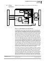
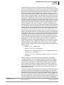
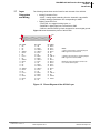
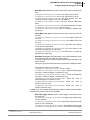
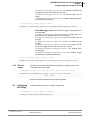
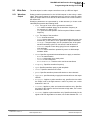
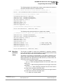
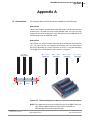
DNx-AO-364 — User Manual 4-Channel Function Generator/AWFG Interface Board for the PowerDNA Cube and PowerDNR RACKtangle Release 4.7 September 2013 PN Man-DNx-AO-364-913 © Copyright 1998-2013 United Electronic Industries, Inc. All rights reserved. No part of this publication may be reproduced, stored in a retrieval system, or transmitted, in any form by any means, electronic, mechanical, by photocopying, recording, or otherwise without prior written permission. Information furnished in this manual is believed to be accurate and reliable. However, no responsibility is assumed for its use, or for any infringement of patents or other rights of third parties that may result from its use. All product names listed are trademarks or trade names of their respective companies. See the UEI website for complete terms and conditions of sale: http://www.ueidaq.com/cms/terms-and-conditions/ Contacting United Electronic Industries Mailing Address: 27 Renmar Avenue Walpole, MA 02081 U.S.A. For a list of our distributors and partners in the US and around the world, please see http://www.ueidaq.com/partners/ Support: Telephone: Fax: (508) 921-4600 (508) 668-2350 Also see the FAQs and online “Live Help” feature on our web site. Internet Support: Support: Web-Site: FTP Site: [email protected] www.ueidaq.com ftp://ftp.ueidaq.com Product Disclaimer: WARNING! DO NOT USE PRODUCTS SOLD BY UNITED ELECTRONIC INDUSTRIES, INC. AS CRITICAL COMPONENTS IN LIFE SUPPORT DEVICES OR SYSTEMS. Products sold by United Electronic Industries, Inc. are not authorized for use as critical components in life support devices or systems. A critical component is any component of a life support device or system whose failure to perform can be reasonably expected to cause the failure of the life support device or system, or to affect its safety or effectiveness. Any attempt to purchase any United Electronic Industries, Inc. product for that purpose is null and void and United Electronic Industries Inc. accepts no liability whatsoever in contract, tort, or otherwise whether or not resulting from our or our employees' negligence or failure to detect an improper purchase. Specifications in this document are subject to change without notice. Check with UEI for current status. 1 Table of Contents Chapter 1 Introduction .................................................... 3 1.1 Organization of Manual. . . . . . . . . . . . . . . . . . . . . . . . . . . . . . . . . . . . . . . . . . . . . . . . 3 1.2 The AO-364 Interface Board. . . . . . . . . . . . . . . . . . . . . . . . . . . . . . . . . . . . . . . . . . . . 5 1.3 Features . . . . . . . . . . . . . . . . . . . . . . . . . . . . . . . . . . . . . . . . . . . . . . . . . . . . . . . . . . . 6 1.4 Indicators . . . . . . . . . . . . . . . . . . . . . . . . . . . . . . . . . . . . . . . . . . . . . . . . . . . . . . . . . . 6 1.5 Specification . . . . . . . . . . . . . . . . . . . . . . . . . . . . . . . . . . . . . . . . . . . . . . . . . . . . . . . . 7 1.6 Device Architecture. . . . . . . . . . . . . . . . . . . . . . . . . . . . . . . . . . . . . . . . . . . . . . . . . . . 8 1.7 Layer Connectors and Wiring . . . . . . . . . . . . . . . . . . . . . . . . . . . . . . . . . . . . . . . . . . 10 Chapter 2 Programming with the High Level API . . . . . . . . . . . . . . . . . . . . . . . . . . . . . . 11 2.1 Creating a Session . . . . . . . . . . . . . . . . . . . . . . . . . . . . . . . . . . . . . . . . . . . . . . . . . . 11 2.2 Configuring the Resource String. . . . . . . . . . . . . . . . . . . . . . . . . . . . . . . . . . . . . . . . 11 2.3 2.3.1 2.3.2 Output . . . . . . . . . . . . . . . . . . . . . . . . . . . . . . . . . . . . . . . . . . . . . . . . . . . . . . . . . . . . 11 Waveform Output. . . . . . . . . . . . . . . . . . . . . . . . . . . . . . . . . . . . . . . . . . . . . . 11 DC level Output . . . . . . . . . . . . . . . . . . . . . . . . . . . . . . . . . . . . . . . . . . . . . . . 13 2.4 Configuring the Timing . . . . . . . . . . . . . . . . . . . . . . . . . . . . . . . . . . . . . . . . . . . . . . . 13 2.5 2.5.1 2.5.2 2.5.3 Write Data . . . . . . . . . . . . . . . . . . . . . . . . . . . . . . . . . . . . . . . . . . . . . . . . . . . . . . . . . Waveform Output. . . . . . . . . . . . . . . . . . . . . . . . . . . . . . . . . . . . . . . . . . . . . . Waveform parameter sweep . . . . . . . . . . . . . . . . . . . . . . . . . . . . . . . . . . . . . DC Level Output . . . . . . . . . . . . . . . . . . . . . . . . . . . . . . . . . . . . . . . . . . . . . . 2.6 Cleaning-up the Session. . . . . . . . . . . . . . . . . . . . . . . . . . . . . . . . . . . . . . . . . . . . . . 17 14 14 15 17 Chapter 3 Programming with the Low-level API . . . . . . . . . . . . . . . . . . . . . . . . . . . . . . . 18 © Copyright 2013 United Electronic Industries, Inc. Tel: 508-921-4600 Date: September 2013 www.ueidaq.com Vers: 4.7 DNx-AO-364-ManualTOC.fm 2 List of Figures Chapter 1 – Introduction . . . . . . . . . . . . . . . . . . . . . . . . . . . . . . . . . . . . . . . . . . . . . . . . . . . . . 1 1-1 Block Diagram of the AO-364 Layer ..............................................................................8 1-2 Pinout Diagram of the AO-364 Layer ..........................................................................10 A-1 Pinout and photo of DNA-STP-62 screw terminal panel..............................................19 © Copyright 2013 United Electronic Industries, Inc. Tel: 508-921-4600 Date: September 2013 www.ueidaq.com Vers: 4.7 DNx-AO-364-ManualLOF.fm DNA/DNR-AO-364 Function Generator Board Chapter 1 Introduction Chapter 1 Introduction This document outlines the feature set and use of the DNR- and DNA-AO-364 layer. The AO-364 is a 4-channel function generator analog output module for the PowerDNA I/O Cube (DNA-AO-364) and the DNR-1G HalfRACK and RACKtangle chassis (DNR-AO-364). The DNR version is identical to the DNA version except that the DNR version is designed to plug into a RACKtangle backplane instead of a Cube chassis. 1.1 Organization of Manual This AO-364 User Manual is organized as follows: • Introduction This chapter provides an overview of DNx-AO-364 function generator analog output board features, device architecture, connectivity, and logic. • Programming with the High-Level API This chapter provides an overview of the how to create a session, configure the session, and generate output on the DNx-AO-364 with the UEIDAQ High-level Framework API. • Programming with the Low-Level API This chapter is an overview of low-level API commands for configuring and using the AO-364 series layer. • Appendix A - Accessories This appendix provides a list of accessories available for use with the DNx-AO-364 board. • Index This is an alphabetical listing of the topics covered in this manual. NOTE: A glossary of terms used with the PowerDNA Cube/Rack and layers can be viewed and/or downloaded from www.ueidaq.com. © Copyright 2013 United Electronic Industries, Inc. Tel: 508-921-4600 Date: September 2013 www.ueidaq.com Vers: 4.7 DNx-AO-364 Chap1x.fm 3 DNA/DNR-AO-364 Function Generator Board Chapter 1 Introduction Manual Conventions To help you get the most out of this manual and our products, please note that we use the following conventions: Tips are designed to highlight quick ways to get the job done or to reveal good ideas you might not discover on your own. NOTE: Notes alert you to important information. CAUTION! Caution advises you of precautions to take to avoid injury, data loss, and damage to your boards or a system crash. Text formatted in bold typeface generally represents text that should be entered verbatim. For instance, it can represent a command, as in the following example: “You can instruct users how to run setup using a command such as setup.exe.” Text formatted in fixed typeface generally represents source code or other text that should be entered verbadim into the source code, initialization, or other file. Examples of Manual Conventions Before plugging any I/O connector into the Cube or RACKtangle, be sure to remove power from all field wiring. Failure to do so may cause severe damage to the equipment. Usage of Terms Throughout this manual, the term “Cube” refers to either a PowerDNA Cube product or to a PowerDNR RACKtangle rack mounted system, whichever is applicable. The term DNR is a specific reference to the RACKtangle, DNA to the PowerDNA I/O Cube, and DNx to refer to both. © Copyright 2013 United Electronic Industries, Inc. Tel: 508-921-4600 Date: September 2013 www.ueidaq.com Vers: 4.7 DNx-AO-364 Chap1x.fm 4 DNA/DNR-AO-364 Function Generator Board Chapter 1 Introduction 1.2 The AO-364 Interface Board The DNA-AO-364 and DNR-AO-364 are 4 channel function generator/Arbitrary Waveform Generator (AWFG) boards designed for use in UEI’s popular Cube and RACKtangle chassis, respectively. Standard sine, square, pulse, triangle, sawtooth, and trapezoid waveforms at up to 150 kHz are provided, or the user may create a custom waveform by taking advantage of the boards’ AWFG capabilities. Each channel’s output may be set independently of the others or may be slaved to any other channel taking advantage of the programmable phase shift functionality. The DNx-AO-364 provides high resolution in both its frequency output as well as voltage output settings. Output Frequency may be set from 1mHz to 150 kHz with 0.25 Hz resolution and ±1.0 Hz overall accuracy. Output voltages may be set from 0 to 8.45 Vrms with 16-bit resolution. Output DC offset may be set between ±12 VDC, also with 16-bit resolution. Note that total output voltage selected including output voltage and offset may not exceed ±12 VDC. The outputs may be enabled or disabled under software control with output impedances of <1 Ohm or >150 kOhm respectively. Phase is programmable 0 to 360 degrees relative to any other channel on the board as well as relative to a “master” channel on another AO-364 series board. This phase shift may be set in increments of <0.1°. Square wave duty cycle is also programmable from 0 to 100% in 0.25% increments in DDS mode. Outputs may be swept over frequency and/or output voltage/offset. The sweep range takes advantage of the boards AWFG capability and so may be set in to output sweep function that can be created based on discrete 50 ns updates. Single Ramp (Freq A to Freq B and then hold at Freq B), Cycle Ramp (Freq A to Freq B to Freq A and hold at Freq A) or Continuous (Freq A to Freq B to Freq A to Freq B and so on). The sweep control may be set from the host PC at update rates up to 1 kHz. The board also performs as a powerful Arbitrary Waveform Generator, with 60.6 ns updates. The 8 Megasample AWFG memory allows the user to create almost any desired output wave shape. The AWFG generator outputs swing from +12 to -12 VDC. All connections are made through standard DB-62 connectors, making it easy for OEMs to design custom cabling. For end-user applications or proof of concept OEM applications, UEI also provides the easy to use DNA-STP-62 screw terminal panel. The DNA-CBL-62 series cable connects the DNx-AO-364 to the DNA-STP-62 screw terminal board and is available in lengths of 1, 3, 5, 10 and 20 feet. The DNA/DNR-AO-364 is supported by the UEIDAQ Framework providing a simple and complete software interface to all popular Windows programming languages and DAQ applications including LabVIEW, MATLAB and DasyLAB. An extensive factory written software driver is also provided for all popular “nonWindows” operating systems including Linux, VXworks, QNX, RTX, INtime and more. © Copyright 2013 United Electronic Industries, Inc. Tel: 508-921-4600 Date: September 2013 www.ueidaq.com Vers: 4.7 DNx-AO-364 Chap1x.fm 5 DNA/DNR-AO-364 Function Generator Board Chapter 1 Introduction 1.3 1.4 Features Indicators The AO-364 layer has the following features: • 4 independently configurable channels • DC, Sine, Square, Pulse, Triangle, Sawtooth, Trapezoid, or Arbitrary Waveform Function Generator (AWFG) output • 0.1 to 150 kHz output frequency • 0.25 Hz output resolution • Software selectable phase shift between channels • Real-time frequency slew/sweep • 350 Vrms channel-to-channel isolation • Weight of 136 g or 4.79 oz for DNA-AO-364; 817 g or 28.8 oz with Cube. • Tested to withstand 5g Vibration, 50g Shock, -40 to +85°C Temperature, and Altitude up to 70000 ft or 21000 meters. A photo of the DNR-AO-364 unit is illustrated below. The front panel has two LED indicators: • RDY: indicates that the layer is receiving power and operational. • STS: can be set by the user using the low-level framework. DNR bus connector RDY LED STS LED DB-62 (female) 62-pin I/O connector The DNR-AO-364 Analog-Output Layer © Copyright 2013 United Electronic Industries, Inc. Tel: 508-921-4600 Date: September 2013 www.ueidaq.com Vers: 4.7 DNx-AO-364 Chap1x.fm 6 DNA/DNR-AO-364 Function Generator Board Chapter 1 Introduction 1.5 Specification The technical specification for the DNx-AO-364 board are listed in Table 1-1. Table 1-1. DNx-AO-364 Technical Specifications General Specifications /VNCFSPGDIBOOFMT 0VUQVUUZQF 0VUQVU)BSNPOJD%JTUPSUJPO 0VUQVUSBOHF 0VUQVUESJWF 0VUQVUSFTPMVUJPO 0VUQVUTMFXSBUF 0VUQVU%$PòTFU %$PòTFUSFTPMVUJPO 0VUQVUTUBUFTJNQFEBODF Frequency Specifications 0VUQVU3BOHF 0VUQVU'SFR3FTPMVUJPO 0VUQVU'SFR"DDVSBDZ Phase shift control $POöHVSBUJPO JOEFQFOEFOUMZDPOöHVSBCMF 4JOF4RVBSF1VMTF5SJBOHMF5SBQF[PJE%$"8'( E#BUL)[E#BUMFTTUIBOL)[ UP7SNT7%$ N"NJO CJU 7PMUNJDSPTFDPOE 7%$OPUFNBYPVUQVUJODMVEJOH7PVUBOE PòTFUJT7%$ CJU &OBCMFE0IN %JTBCMFEL0IN 1mHz to 150 kHz )[BQQSPYJNBUFMZCJUT )[PSCFUUFS 4MBWFESFMBUJWFUPBOZDIBOOFM.BZCFTMBWFEUP DIBOOFMTPOPUIFS%/Y"0CPBSET 1IBTFTIJGUSBOHFSFTPMVUJPO ¡¡ Duty cycle control %VUZDZDMFSBOHF UP %VUZDZDMFSFTPMVUJPO JO%%4NPEF Sweep Control 4XFFQVQEBUFSBUF NTNBYGSPNIPTU1$ 4XFFQ'SFRVFODZ3BOHF 'VMMTDBMFN)[UPL)[ BOZUJNJOHQPTTJCMF within 50 ns sample update rate "NQMJUVEFPòTFUSBOH 'VMMTDBMF7%$ 4XFFQNPEFT 4JOHMF3BNQ$ZDMF3BNQ$POUJOVPVT3BNQ AWFG specifications 0VUQVUUJNJOHSFTPMVUJPO OT 0VUQVUXBWFGPSNTJ[F .FHBTBNQMFQFSDIBOOFM General Specifications Isolation 7DIBOOFMUPDIBOOFMBOEDIBOOFMUPDIBTTJT &4%QSPUFDUJPO L7 1PXFS$POTVNQUJPO 8TIPVMEOPUCFQMBDFEJOBEKBDFOUTMPUT 0QFSBUJOH5FNQFSBUVSF 5FTUFEUP¡$ 0QFSBUJOH)VNJEJUZ OPODPOEFOTJOH 7JCSBUJPOIEC 60068-2-6 H)[TJOVTPJEBM IEC 60068-2-64 HSNT )[CSPBECBOESBOEPN HNTIBMGTJOFTIPDLT!PSJFOUBUJPOT 4IPDLIEC 60068-2-27 HNTIBMGTJOFTIPDLT!PSJFOUBUJPOT Note: A rear-mount fan such as the DNA-FAN3 (for 3-layer Cube), DNA-FAN5 (for 5-layer Cube), or FAN-925 (for RACKtangle) and filler plates should be used to avoid high ambient temperatures. © Copyright 2013 United Electronic Industries, Inc. Tel: 508-921-4600 Date: September 2013 www.ueidaq.com Vers: 4.7 DNx-AO-364 Chap1x.fm 7 DNA/DNR-AO-364 Function Generator Board Chapter 1 Introduction Figure 1-1 is a block diagram of the architecture of the AO-364 layer. I/O Connector 8MS RAM 4kS RAM Channel Control Logic CLK (or DIO0) TRIG (or DIO1) DDS PLL PLL Main Control Logic GND AGND AOUT 1.43x Buffer 1/2/5/10x PGA OUT IN OFFSET EEPROM 16-bit ±1V 16.5MHz max main DAC 18-bit ±10V 1MHz max offset DAC 32-bit 66MHz bus Device Architecture Optical Isolation 1.6 Isolated DC/DC Figure 1-1. Block Diagram of the AO-364 Layer The DNA/DNR-AO-364 Function Generator Board has four individual analog output channels, seen in Figure 1-1. On the right, connected to the DNA bus, the main controller is field-programmable and is optically isolated from each of the four channels that it manages. Each channel has its own individual programmable logic controller (PLC) controlling the output circuitry: main DAC, offset DAC, PGA, and output buffer; with two isolated power supplies per channel. The main DAC (±1V, 16-bit steps, 16.5MHz or 60.6ns update rate max) is the input to a 1/2/5/10x PGA. The PGA also uses for reference a ±10V offset DAC (18-bit steps, 1MHz update rate max). The PGA output is buffered with gain of 1.2x for a 12.0 max voltage span while supplying up to 25mA load current; and can be en/disabled in software with impedence <1Ω or >150kΩ respectively. On the DB-62 connector the buffer’s output is wired to the channel’s AOUT pin and the return line on the AGND pin, designed to be connected by twisted-pair wire. For analog signals, use only AOUT and AGND, and not the channel’s reference ground line (GND) which is also used as the digital input/output ground. Output voltages can be programmed from 0 to 8.45 Vrms with 16-bit resolution. Output DC offset may be set between ±12.0 VDC, also with 16-bit resolution. Output Frequency may be set from smaller than 1millihertz up to 150 kHz. The channel’s controller can be thought of as capable of 2 modes of operation: Function Generator mode and Advanced Waveform Function Generator mode. In Function Generator mode the PLC's internal 4096 x 16-bit sample memory provides data for direct digital synthesis (DDS) or a phase-locked loop (PLL). Information is available online and in various books on the operation and advantages and disadvantages of choosing either DDS or PLL to generate a waveform; thus the capabilities of the AO-364 to generate each is explained briefly. Both DSS and PLL mode have programmable voltage offset, span, and phase © Copyright 2013 United Electronic Industries, Inc. Tel: 508-921-4600 Date: September 2013 www.ueidaq.com Vers: 4.7 DNx-AO-364 Chap1x.fm 8 DNA/DNR-AO-364 Function Generator Board Chapter 1 Introduction control, but frequency sweep is programmable only in DSS and not for PLL. The Function Generator in PLL mode offers less harmonics and jitter (deviation from the true periodicity of the waveform) than DDS, and PLL mode is better for waveforms with sharp edges (pulse, trapezoid) at higher frequencies (100kHz+) than DDS, but at low frequencies DDS is within 0.001Hz versus PLL’s 0.1Hz. In PLL mode the DAC clock is created using two groups of cascaded PLLs set to the “closest calculated frequency” that matches the user-selected output frequency. Each resulting clock edge is used to read one sample out of the 4096 sample buffer. If the frequency is slower than the number of samples in the buffer, and since the type of waveform is user-programmed as a sine, pulse, or trapezoid, the logic will create additional samples (sub- or super-sample) to create a smooth output; if the frequency is faster, only every few samples will be read instead. Programming PLL mode for operation consumes 500-800ms which effectively limits using PLL mode from performing frequency sweep operations. The Function Generator in DDS mode allows you to select an exact frequency to within 0.001Hz, but has slightly more harmonics and introduces jitter into any waveform with sharp edges that becomes more evident at higher frequencies. Frequency Generation mode generates sine, pulse (e.g. square), trapezoid (e.g. triangle, sawtooth) waveforms up to 150kHz. Each channel's output may be set independently of the others, or it may be slaved to another channel on the board or relative to a "master" channel on another AO-364 series board in the Cube or RACKtangle. Slaved channels may have their timing programmed to follow a "master" channel's signal. Slave channels can be programmed to have a relative phase-shift of 0° to 360° from its master, set in increments of less than 0.1°. Square wave duty cycle is also programmable from 0.03% to 99.97% in increments of 1/4096 or 0.25% in DDS mode. Outputs may be swept over DDS frequency, DDS phase, DAC digital out gain, DAC offset value, output voltage/ offset. In Function Generator (FG) mode the sweep functions can operate in the following modes: • Sweep F1 to F2, Single Sweep • Sweep F1 to F2 to F1, Single Sweep • Sweep F1 to F2, Continuous: sweeps F1 to F2, immediate change to F1, sweep F1 to F2, and repeat. • Sweep F1 to F2 to F1, Continuous: sweeps F1 to F2 to F1 to F2 to F1 and repeat where F1 and F2 are initial and ending function parameters, respectively. In Arbitrary Waveform Function Generator (AWFG) mode the PLC reads the user-generated samples from the PSRAM (4096S per channel, up to 8MS in new revisions) and produces an output waveform. AWFG mode cannot use DDS or make use of frequency of phase sweeps for waveforms not equal to 4096 samples. Sweep functions in AWFG mode can be created based on pregenerated discrete samples. The frequency may be set from the host PC at update rates up to 1 kHz. In addition to controlling analog output lines, the channel controller logic is wired to process and make use of the digital lines marked DIO0:1, CLK and TRIG. Note that the digital ground reference line is GND (not AGND or analog ground). Each channel may be individually configured in software to have its trigger/clock source be (i) any another channel’s CLK/TRIG pins on the same AO-364, or (ii) the master channel (i.e. Ch0) of another board where that board’s trigger/clock may be propagated using the internal sync bus of that Cube or RACKtangle. © Copyright 2013 United Electronic Industries, Inc. Tel: 508-921-4600 Date: September 2013 www.ueidaq.com Vers: 4.7 DNx-AO-364 Chap1x.fm 9 DNA/DNR-AO-364 Function Generator Board Chapter 1 Introduction 1.7 Layer Connectors and Wiring The following connections can be found for each channel of the AO-364: • Analog Connection Pins: - AOUT: analog output extending from the channel’s output buffer. - AGND: analog ground/return line corresponding to AOUT. • Digital Connection Pins: - CLK/TRIG: the trigger/clocking inputs, or - DIO0/DIO1: digital input lines, referenced to GND. - GND: the board’s DC/DC ground; designed for use as digital ground. Figure 1-2 below illustrates the pinout of the AO-364. SHIELD Pin Signal /$ /$ /$ "(/% (/% /$ $-, /$ "(/% (/% /$ /$ /$ "(/% (/% /$ $-, /$ (/% (/% /$ Pin Signal /$ (/% 53*( "065 347% /$ (/% (/% "065 347% /$ (/% 53*( "065 347% /$ (/% (/% (/% 347% /$ Pin Signal (/% $-, (/% (/% /$ /$ 53*( /$ (/% (/% (/% $-, (/% (/% /$ /$ 53*( /$ "(/% "065 Notes: $-,ODBOCFVTFEBTBHFOFSBMQVSQPTF %*0TJHOBMJGOPUVTFEBT$-, 53*(ODBOCFVTFEBTBHFOFSBMQVSQPTF %*0TJHOBMJGOPUVTFEBT53*( 347%QJOTBSFGPSJOUFSOBMVTF1MFBTFEP not connect to these pins. Figure 1-2. Pinout Diagram of the AO-364 Layer © Copyright 2013 United Electronic Industries, Inc. Tel: 508-921-4600 Date: September 2013 www.ueidaq.com Vers: 4.7 DNx-AO-364 Chap1x.fm 10 DNA/DNR-AO-364 Function Generator Board Chapter 2 Programming with the High Level API Chapter 2 Programming with the High Level API This section describes how to control the DNx-AO-364 using the UeiDaq Framework High Level API. UeiDaq Framework is object oriented and its objects can be manipulated in the same manner from different development environments such as Visual C++, Visual Basic or LabVIEW. The following section focuses on the C++ API, but the concept is the same no matter what programming language you use. Please refer to the “UeiDaq Framework User Manual” for more information on use of other programming languages. 2.1 Creating a Session The Session object controls all operations on your PowerDNx device. Therefore, the first task is to create a session object: // create a session object for input CUeiSession wfmSession; 2.2 Configuring UeiDaq Framework uses resource strings to select which device, subsystem the Resource and channels to use within a session. The resource string syntax is similar to a web URL: String <device class>://<IP address>/<Device Id>/<Subsystem><Channel list> For PowerDNA and RACKtangle, the device class is pdna. The AO-364 is programmed using the subsystem ao. For example, the following resource string selects analog output channels 0,1,2 on device 1 at IP address 192.168.100.2: “pdna://192.168.100.2/Dev1/Ao0:2” as a range, or as a list “pdna://192.168.100.2/Dev1/Ao0,1,2”. 2.3 2.3.1 Output Waveform Output The AO-364 can be configured for waveform output or constant DC level output. The AO-364 can be configured for waveform output with the CreateAOWaveformChannel function call, as follows: // Configure channel 0 of an AO-364 set as device 1: session.CreateAOWaveformChannel("pdna://192.168.100.2/Dev1/ao0", UeiAOWaveformClockSourcePLL, UeiAOWaveformOffsetClockSourceSW, UeiAOWaveformClockRouteNone); CreateAOWaveformChannel configures the following parameters: © Copyright 2013 United Electronic Industries, Inc. Tel: 508-921-4600 Date: September 2013 www.ueidaq.com Vers: 4.7 DNx-AO-364 Chap2x.fm 11 DNA/DNR-AO-364 Function Generator Board Chapter 2 Programming with the High Level API • Main DAC clock source: The source of the clock used to time the main DAC: UeiAOWaveformClockSourceSYNC2: use SYNC2 line for clock UeiAOWaveformClockSourceSYNC0: use SYNC0 line for clock UeiAOWaveformClockSourceALT0: use layer channel zero PLL routed to Channel 0 trigger out to clock all channels UeiAOWaveformClockSourceTMR: clock from internal TMR0 timebase UeiAOWaveformClockSourceDIO0: use channel DIO0 line for clock UeiAOWaveformClockSourcePLL: clock from PLL UeiAOWaveformClockSourceSW: DAC is clocked by software (DC offset only) • Offset DAC clock source: The source of the clock used to time the offset DAC: UeiAOWaveformOffsetClockSourceDIO0: use channel DIO0 line for clock UeiAOWaveformOffsetClockSourceDIO1: use channel DIO1 line for clock UeiAOWaveformOffsetClockSourceDAC: main DAC clock divided is the source of offset DAC UeiAOWaveformOffsetClockSourcePLL: PLL is the source of the offset DAC (independent of main DAC) UeiAOWaveformOffsetClockSourceSW: offset DAC is clocked by software (DC offset only) • Main DAC clock sync: Specifies where a clock signal should be routed to synchronize with other channels and/or layers. Route your signal out to TrgOut to synchronize multiple channels on the same AO-364. Route your signal out to the Sync lines to synchronize multiple AO-364s. Only valid for channel 0 on AO-364: UeiAOWaveformClockRouteNone: No sync routing UeiAOWaveformClockRouteDIO1ToTrgOut: Route the DIO1/trigger input pin to Channel0 trigger out (channel 0 only) UeiAOWaveformClockRouteDIO0ToTrgOut: Route the DIO0/clock input pin to Channel0 trigger out (channel 0 only) UeiAOWaveformClockRoutePLLToTrgOut: Route PLL clock to Channel0 trigger out (channel 0 only) UeiAOWaveformClockRoutePLLToSYNC2: Route PLL clock to SYNC2 (channel 0 only) UeiAOWaveformClockRoutePLLToSYNC0: Route PLL clock to SYNC0 (channel 0 only) In addition you can set additional parameters using the following channel object methods (or a property node under LabVIEW): • © Copyright 2013 United Electronic Industries, Inc. Main DAC trigger source: source used to trigger a new period out of the main DAC: UeiAOWaveformTriggerSourceNone: no trigger, layer outputs when clock is available UeiAOWaveformTriggerSourceCH0: channel 0 will deliver clock triggered on CH0_TRIGIN line UeiAOWaveformTriggerSourceSYNC3: use SYNC3 line as a trigger UeiAOWaveformTriggerSourceSYNC1: use SYNC1 line as a trigger Tel: 508-921-4600 Date: September 2013 www.ueidaq.com Vers: 4.7 DNx-AO-364 Chap2x.fm 12 DNA/DNR-AO-364 Function Generator Board Chapter 2 Programming with the High Level API UeiAOWaveformTriggerSourceALT0: use channel 0 CH0-TIN line for trigger (needs to be connected to a source) UeiAOWaveformTriggerSourceDIO1: use channel DIO1 line for trigger UeiAOWaveformTriggerSourceSW: use software trigger (simultaneous only within single layer) // Set main DAC trigger source to DIO1 pWfmChan->SetMainDACTriggerSource(UeiAOWaveformTriggerSourceDIO1); • Offset DAC trigger source: source used to trigger a new period out of the offset DAC: UeiAOWaveformOffsetTriggerSourceNone: no trigger, layer outputs when clock is available (use with NIS clocking) UeiAOWaveformOffsetTriggerSourceSYNC3: use SYNC3 line as a trigger UeiAOWaveformOffsetTriggerSourceSYNC1: use SYNC1 line as a trigger UeiAOWaveformOffsetTriggerSourceALT0: use channel 0 CH0TIN line for trigger (needs to be connected to a source) UeiAOWaveformOffsetTriggerSourceDIO1: use channel DIO1 line for trigger UeiAOWaveformOffsetTriggerSourceSW: use software trigger (simultaneous only within single layer) // Set offset DAC trigger source to DIO1 pWfmChan->SetOffsetDACTriggerSource(UeiAOWaveformOffsetTriggerSourceDIO1); 2.3.2 DC level Output Use the function call CreateAOChannel as follows to configure one or more channel(s) in DC output mode: // Configure channel 0 of an AO-364 set as device 1 for DC output: wfmSession.CreateAOChannel(“pdna://192.168.100.2/Dev0/ao0”, -10.0, 10.0); Note that the last two parameters are presently ignored. 2.4 Configuring the Timing Configure the AO-364 to run in “simple” timing mode. // configure timing of input to “simple” wfmSession.ConfigureTimingForSimpleIO(); © Copyright 2013 United Electronic Industries, Inc. Tel: 508-921-4600 Date: September 2013 www.ueidaq.com Vers: 4.7 DNx-AO-364 Chap2x.fm 13 DNA/DNR-AO-364 Function Generator Board Chapter 2 Programming with the High Level API 2.5 2.5.1 Write Data Waveform Output The writer object is used to output a waveform or set up a DC level signal. Setting waveform parameters for the AO-364 outputs is done using a writer object. Each output channel is independent and you need to create one writer object per output channel to be able to set the waveform out of each channel in the channel list. Waveform parameters are represented by a data structure (or cluster under LabVIEW) that contains the following fields: © Copyright 2013 United Electronic Industries, Inc. • mode: The type of clock used to generate the waveform: - DDS: allows immediate change in the waveform frequency at the expense of a higher THD - PLL: gives the lowest possible THD but requires 500ms to switch frequency • type: The shape of the waveform: - Sine: sinusoid waveform - Pulse: square shape waveform with programmable duty-cycle, rise and fall time. It can also be set to generate a trapezoid waveform. - Triangle: Triangular shape, this is a particular case of the pulse waveform with duty-cycle=0.0, rise time=0.5 and fall-time=0.5. - Sawtooth: outputs a linear ramp going from min amplitude to max amplitude. - Custom: custom waveform uploaded by user to a 4096 sample hardware buffer. • xForm: Specifies a geometrical transformation to apply to waveform: - None: No transformation - Mirror: Horizontally mirror each period - Invert: Invert each period - MirrorAndInvert: Combine mirror and invert transforms • frequency: Specifies waveform frequency • span: Specifies waveform peak to peak amplitude • offset: Specifies waveform DC offset • phase: Specifies waveform phase shift relative to other channels • applyTime: specifies a delay to apply the new waveform on the output channel • dutyCycle: Applies to pulse waveform only, specifies the time while the output is set in the high state as a ratio of a period; use a value between 0.0 and 1.0 • riseTime: Applies to pulse and sawtooth waveforms only. Specifies the delay for the signal to rise from low state to high state; use a value between 0.0 and 1.0 • fallTime: Applies to pulse waveform only. Specifies the delay for the signal to fall from high state to low state; use a value between 0.0 - 1.0 Tel: 508-921-4600 Date: September 2013 www.ueidaq.com Vers: 4.7 DNx-AO-364 Chap2x.fm 14 DNA/DNR-AO-364 Function Generator Board Chapter 2 Programming with the High Level API The following sample code shows how to create a writer object tied to channel 2 and set the waveform output to a 10kHz sine wave. // create a writer and link it to the session’s stream, port 2 writer = new CUeiAOWaveformWriter(wfmSession.GetDataStream(), 2); // configure writer for sine waveform, 10kHz tUeiAOWaveformParameters wfmParams; wfmParams.mode = UeiAOWaveformModeDDS; wfmParams.type = UeiAOWaveformTypeSine; fmParams.frequency =10000.0; wfmParams.span = 8.0; wfmParams.offset =0.0; wfmParams.phase =0.0; wfmParams.applyTime = 0.0; // write waveform configuration to the hardware writer->WriteWaveform(1, &wfmParams, NULL); The following code sets the waveform to a square wave, instead: // configure writer for square wave (pulse waveform with 50% duty cycle) wfmParams.mode = UeiAOWaveformModeDDS; wfmParams.type = UeiAOWaveformTypePulse; fmParams.frequency =10000.0; wfmParams.span = 8.0; wfmParams.offset =0.0; wfmParams.phase =0.0; wfmParams.riseTime = 0.0; wfmParams.fallTime = 0.0; wfmParams.dutyCycle = 0.5; wfmParams.applyTime = 0.0; // 10kHz // sharp rising edge // sharp falling edge // 50% duty cycle writer->WriteWaveform(1, &wfmParams, NULL); 2.5.2 Waveform parameter sweep The AO-364 is capable of varying any combination of waveform frequency, span, offset and phase. The sweep operation is programmed and started using the same writer object used to set the waveform shape. The duration of the sweep is programmable. It can either be specified in seconds or as a number of steps to be evenly spread across a number of periods. Sweep parameters are represented by a data structure (or cluster under LabVIEW) that contains the following fields: • © Copyright 2013 United Electronic Industries, Inc. control: Controls the sweep operation, with parameters: - UpStart: Starts sweeping parameters from the lower value to the upper value - DownStart: Starts sweeping parameters from the upper value to the lower value - UpDownStart: Starts sweeping parameters from the lower value to the upper value and back to the lower value - DownUpStart: Starts sweeping parameters from the upper value to the lower value and back to the upper value - Stop: Stops any on-going sweep Tel: 508-921-4600 Date: September 2013 www.ueidaq.com Vers: 4.7 DNx-AO-364 Chap2x.fm 15 DNA/DNR-AO-364 Function Generator Board Chapter 2 Programming with the High Level API • mode: the mode of the sweep - Continuous: automatically re-start sweep operation - SingleShot: run sweep only once • sweepTime: specifies the duration of the sweep in seconds. When set to 0.0 secs the numberOfPeriods, stepsUp and stepsDown fields are used to set the duration. • numberOfPeriods: is an alternate way to specify the sweep duration • stepsUp: number of steps used to sweep from lower to upper values • stepsDown: number of steps used to sweep from upper to lower values • lowerFrequency: the lower frequency value • upperFrequency: the upper frequency value • lowerAmplitude: the lower amplitude value • upperAmplitude: the upper amplitude value • lowerOffset: the lower offset value • upperOffset: the upper offset value • lowerPhase: the lower phase value • upperPhase: the upper phase value Set both the lower and upper values to 0.0 to disable any of the four parameter sweep(s). The following sample code shows how to sweep frequency from 10Hz to 1000Hz in 10 seconds: // configure writer to sweep from 10-1000 Hz in 10 sec tUeiAOWaveformSweepParameters sweepParams; sweepParams.control = UeiAOWaveformSweepUpStart; sweepParams.mode = UeiTimingDurationSingleShot sweepParams.sweepTime = 10.0 sweepParams.lowerFrequency = 10.0 sweepParams.upperFrequency = 1000.0 sweepParams.lowerAmplitude = 0.0 sweepParams.upperAmplitude = 0.0 sweepParams.lowerOffset = 0.0 sweepParams.upperOffset = 0.0 sweepParams.lowerPhase = 0.0 sweepParams.upperPhase = 0.0 // write waveform configuration to the hardware writer->WriteSweep(1,&sweepParams, NULL); © Copyright 2013 United Electronic Industries, Inc. Tel: 508-921-4600 Date: September 2013 www.ueidaq.com Vers: 4.7 DNx-AO-364 Chap2x.fm 16 DNA/DNR-AO-364 Function Generator Board Chapter 2 Programming with the High Level API 2.5.3 DC Level Output Writing data is done using writer object(s). There is a writer object that writes raw data straight to the D/A converter. There is also a writer object that writes data scaled to volts where the framework will perform the conversion to binary codes before sending the data to the D/A converter. The following sample code shows how to create a scaled writer object and write a sample. // create a writer and link it to the session’s stream CueiAnalogScaledWriter writer(session.GetDataStream()); // the buffer must be big enough to contain one value per channel double data[2] = {0.0, 0.0}; // write one scan, where the buffer will contain one value per channel writer.WriteSingleScan(data); Similarly, you can create a raw writer object by entering the following: // create a writer and link it to the session’s stream CueiAnalogRawWriter writer(session.GetDataStream()); // the buffer must be big enough to contain one value per channel uInt16 data[2] = {0x1234, 0x5678}; // write one scan writer.WriteSingleScan(data); 2.6 Cleaning-up the Session The session object will clean itself up when it goes out of scope or when it is destroyed. To reuse the object with a different set of channels or parameters, you can manually clean up the session as follows: // clean up the session wfmSession.CleanUp(); © Copyright 2013 United Electronic Industries, Inc. Tel: 508-921-4600 Date: September 2013 www.ueidaq.com Vers: 4.7 DNx-AO-364 Chap2x.fm 17 DNA/DNR-AO-364 Function Generator Board Chapter 3 Programming with the Low-level API Chapter 3 Programming with the Low-level API The PowerDNA cube and PowerDNR RACKtangle and HalfRACK can be programmed using the low-level API. The low-level API offers direct access to PowerDNA DAQBios protocol and also allows you to access device registers directly. However, we recommend that, when possible, you use the UeiDaq Framework High-Level API (see Chapter 2), because it is easier to use. You need to use the low-level API only if you are using an operating system other than Windows. For additional information about low-level programming of the AO-364, please refer to the PowerDNA API Reference Manual document under: Start » Programs » UEI » PowerDNA » Documentation Refer to the PowerDNA API Reference Manual on how to use the following lowlevel functions of AO-364, as well as others related to cube operation: Function Description DqAdv364SetConfig DqAdv364SetAWF DqAdv364SetOffsWF DqAdv364WriteAWF DqAdv364WriteOffsWF DqAdv364SelectAWF DqAdv364Write sets configuration for AO-364. creates a new list of buffers for use with AWF generation. sets configuration for offset DAC. writes waveform to AO-364 waveform buffer writes waveform to AO-364 waveform buffer for offset DAC switches to new buffer with loaded AWF, applies new parameters single-scan function that allows to write static values to AO-364 card DqAdv364WriteChannel stops any waveform on that channel and write DC value to it DqAdv364Enable DqAdv364SetWF DqAdv364SetWFSweep DqAdv364SetDIO enables or disables selected channels and enable/disable outputs applies waveform parameters for the channel switch waveform into sweep mode set direction and source for DIO on the channel DqAdv364SetChannelPll Calculates and sends setup values for use by on-layer PLL DqAdv364SetBaseClocks overwrite automatically selected PLL frequencies for output waveforms and/or retrieve true frequencies to check for tolerances © Copyright 2013 United Electronic Industries, Inc. Tel: 508-921-4600 Date: September 2013 www.ueidaq.com Vers: 4.7 DNx-AO-364 Chap3.fm 20 DNA/DNR-AO-364 Function Generator Board Appendix A Appendix A A. Accessories The following cables and STP boards are available for the AO-364 layer. DNA-CBL-62 This is a 62-conductor round shielded cable with 62-pin male D-sub connectors on both ends. It is made with round, heavy-shielded cable; 2.5 ft (75 cm) long, weight of 9.49 ounces or 269 grams; up to 10ft (305cm) for the DNA-CBL-62-10 and 20ft (610cm) for the DNA-CBL-62-20. DNA-STP-62 The STP-62 is a Screw Terminal Panel with three 20-position terminal blocks (JT1, JT2, and JT3) plus one 3-position terminal block (J2). The dimensions of the STP-62 board are 4w x 3.8d x1.2h inch or 10.2 x 9.7 x 3 cm (with standoffs). The weight of the STP-62 board is 3.89 ounces or 110 grams. DB-62 (female) 62-pin connector: 62 61 60 59 58 57 56 55 54 53 52 51 50 49 48 47 46 45 44 43 UP+ UP+5 UP+5 UP+5 UP+5 UP+5 UP+5 UP+5 UP+5 UP+5 UP+5 UP+5 UP+5 UP+5 UP+5 UP+5 UP+5 UP+5 UP+5 UP+5 42 41 40 39 38 37 36 35 34 33 32 31 30 29 28 27 26 25 24 23 22 UP+ UP+5 UP+5 UP+5 UP+5 UP+5 UP+5 UP+5 UP+5 UP+5 UP+5 UP+5 UP+5 UP+5 UP+5 UP+5 UP+5 UP+5 UP+5 UP+5 UP+5 21 20 19 18 17 16 15 14 13 12 11 10 9 8 7 6 5 4 3 2 1 JT3 — 20-position terminal block: UP+ UP+5 UP+5 UP+5 UP+5 UP+5 UP+5 UP+5 UP+5 UP+5 UP+5 UP+5 UP+5 UP+5 UP+5 UP+5 UP+5 UP+5 UP+5 UP+5 UP+5 44 4 47 GND JT2 — 20-position terminal block: 7 JT1 — 20-position terminal block: J2 — 5-position terminal block: 5 4 3 2 1 4)*&-% (/% SHIELD to J2 to JT1 to JT2 to JT3 Figure A-1. Pinout and photo of DNA-STP-62 screw terminal panel NOTE: Filler plates and a rear mount cooling fan such as the DNA-FAN5 (for 3layer Cube) or DNA-FAN8 (for 5-layer Cube) or FAN-925 (for RACKtangle) should be used with this layer. © Copyright 2013 United Electronic Industries, Inc. Tel: 508-921-4600 Date: September 2013 www.ueidaq.com Vers: 4.7 DNx-AO-364 AppxA.fm 19 20 Index B Block Diagram J Jumper Settings 8 C L Cable(s) 19 Configuring the Resource String Connectors and Wiring 10 Conventions 4 Creating a Session 11 Low-level API 11 11 © Copyright © 2013 Copyright 2013 United Electronic United Electronic Industries,Industries, Inc. Inc. 18 O Organization 3 S Screw Terminal Panels 19 Setting Operating Parameters 6 Specifications 7 Support ii H High Level API 7 Tel: 508-921-4600 Date: September 2013 www.ueidaq.com Vers: 4.7 DNx-AO-364-ManualIX.fm