1
BL1500
C-Programmable Controller
User’s Manual
019-0030 · 070717-D
BL1500 User’s Manual
Part Number 019-0030 • Revision D
Last revised on July 17, 2007 • Printed in U.S.A.
Copyright
© 1999–2007 Rabbit Semiconductor, Inc. • All rights reserved.
Rabbit Semiconductor reserves the right to make changes and improvements to its products without providing notice.
Trademarks
•
•
•
•
®
Dynamic C is a registered trademark of Z-World, Inc.
®
Windows is a registered trademark of Microsoft Corporation
™
PLCBus is a trademark of Z-World, Inc.
®
Hayes Smart Modem is a registered trademark of Hayes Microcomputer
Products, Inc.
Notice to Users
When a system failure may cause serious consequences, protecting life
and property against such consequences with a backup system or safety
device is essential. The buyer agrees that protection against consequences resulting from system failure is the buyer’s responsibility.
This device is not approved for life-support or medical systems.
All Z-World products are 100 percent functionally tested. Additional
testing may include visual quality control inspections or mechanical
defects analyzer inspections. Specifications are based on characterization
of tested sample units rather than testing over temperature and voltage of
each unit. Z-World may qualify components to operate within a range of
parameters that is different from the manufacturer’s recommended range.
This strategy is believed to be more economical and effective. Additional
testing or burn-in of an individual unit is available by special arrangement.
Company Address
Rabbit Semiconductor, Inc.
2900 Spafford Street
Davis, California 95618-6809
USA
Telephone:
Facsimile:
Web Site:
E-Mail:
(530) 757-3737
(530) 753-5141
www.rabbit.com
www.rabbit.com/support/
TABLE OF CONTENTS
About This Manual
vii
Chapter 1: Overview
11
Chapter 2: Getting Started
15
Chapter 3: Subsystems
23
Overview .............................................................................................. 12
Features ........................................................................................... 13
BL1500 .......................................................................................... 13
BL1510 .......................................................................................... 13
BL1520 .......................................................................................... 13
Options and Upgrades .................................................................... 14
Software Development and Evaluation Tools ...................................... 14
Developers Kit Packing List ................................................................ 16
Installing Flash EPROM ....................................................................... 17
Connecting the Prototyping Board to the BL1500 ............................... 18
Connecting the BL1500 to a Host PC ................................................... 20
Development Using the RS-232 Port ............................................... 20
Developing with Optional Serial Interface Board 2 .......................... 21
Establishing Communication ................................................................ 22
Running a Sample Program .................................................................. 22
Interface Overview ............................................................................... 24
Programmable Input/Output ICs (PIOs) ............................................... 25
PIO Modes of Operation ................................................................. 25
PIO 1 ............................................................................................. 26
H3 Signals ....................................................................................27
PIO 2 ............................................................................................ 28
H1 Signals ....................................................................................29
Power-Supervisor Integrated Circuit .................................................... 30
Serial Communication Ports ................................................................. 32
RS-485 ............................................................................................. 32
RS-232 and Programming Ports ....................................................... 33
Modem Communication ................................................................ 33
Analog-to-Digital Converter ................................................................ 34
Extra Conversion ............................................................................. 34
Voltage Reference ............................................................................ 35
Data Conversion ............................................................................. 35
BL1500
Table of Contents s iii
Limitations on Output Range .......................................................... 35
Low-pass Filter ................................................................................ 36
Internal Test Voltages ...................................................................... 36
Drift ................................................................................................. 36
Absolute and Ratiometric Modes ................................................... 36
Bipolar or Unipolar Conditioned Inputs .......................................... 38
Factory-Installed Gain and Bias Resistors .................................... 39
Initial Setup ................................................................................. 39
Representative Analog-to-Digital Setups ....................................40
Setting Up Conditioned Inputs ..................................................... 40
Determine Bias Resistor To Center Span .....................................42
Unipolar Variation ........................................................................42
Choose Best Standard Resistor Values ....................................... 42
Bracketing Input Range ............................................................... 43
Pick Proper Tolerance ..................................................................44
Confirm Performance ...................................................................45
Calibrating the A/D Converter ...................................................... 45
Using Unconditioned Converter Channels ..................................... 46
Real-Time Clock ................................................................................... 47
Chapter 4: System Development
49
Chapter 5: Software Reference
59
Beginning Development ....................................................................... 50
Operating Modes ................................................................................. 51
Running A Program in Run Mode ................................................... 51
Returning To Programming Mode ................................................... 52
EPROM ................................................................................................ 53
Programming EPROM ...................................................................... 54
Developing An RS-485 Network ........................................................... 55
Software Development Options ........................................................... 60
Dynamic C Development Software ....................................................... 60
Dynamic C Manuals ........................................................................ 60
Programmable Input/Output ................................................................. 61
Available PIO Lines ......................................................................... 62
Power-up PIO Configuration ........................................................... 62
Input/Output Software ......................................................................... 63
Shadow Registers ............................................................................ 63
Function Prototypes ....................................................................... 63
Real-Time Clock ................................................................................... 66
Global Time and Date Structure ....................................................... 66
Function Prototypes ....................................................................... 67
iv s Table of Contents
BL1500
Analog-to-Digital Converter Drivers .................................................... 69
Function Prototypes ....................................................................... 69
Controlling XP8300 with PIO 1 Port A .................................................. 73
Function Prototypes ....................................................................... 73
Nonvolatile Storage ............................................................................. 74
Function Prototypes ....................................................................... 74
Support Libraries and Sample Programs ............................................... 76
Appendix A: Troubleshooting
79
Appendix B: Specifications
83
Appendix C: Input/Output Map and Interrupt Vectors
93
Appendix D: Prototyping Board
99
Out of the Box ...................................................................................... 80
Dynamic C Will Not Start ..................................................................... 81
Dynamic C Loses Serial Link ................................................................ 81
BL1500 Repeatedly Resets ................................................................... 81
Common Programming Errors ............................................................... 82
Electrical and Mechanical Specifications ............................................. 84
BL1500 Mechanical Dimensions ..................................................... 85
Prototyping Board ........................................................................... 86
Base Plate ........................................................................................ 87
Jumper and Header Specifications ....................................................... 88
Header H1PIO 2 and Analog Input Signals ................................. 89
Header H2RS-232 Port ................................................................. 90
Header H3PIO 1, RS-485, and Power ............................................ 91
Jumper Configurations .................................................................... 92
Memory Map ....................................................................................... 94
Input/Output Map ................................................................................ 94
Interrupt Vectors .................................................................................. 96
Interrupt Priorities ................................................................................ 97
Prototyping Board .............................................................................. 100
Installing the Prototyping Board ................................................... 102
Sample Circuits ................................................................................... 103
LEDs .............................................................................................. 103
Switches ........................................................................................ 103
Headers ......................................................................................... 103
Buzzer ............................................................................................ 104
RC Filter ......................................................................................... 104
Thermistor ..................................................................................... 104
BL1500
Table of Contents s v
Appendix E: Serial Interface Board 2
105
Appendix F: PLCBus
109
Appendix G: Simulated PLCBus Connection
121
Appendix H: Power Management
131
Index
139
Introduction ....................................................................................... 106
External Dimensions ........................................................................... 107
PLCBus Overview .............................................................................. 110
Allocation of Devices on the Bus ...................................................... 114
4-Bit Devices ................................................................................. 114
8-Bit Devices ................................................................................. 115
Expansion Bus Software ..................................................................... 115
PIO Port Connections ........................................................................ 122
Expansion Boards .......................................................................... 122
Liquid Crystal Displays and Keypads ........................................... 123
Software Drivers ................................................................................. 125
Using Expansion Boards with PIO 1 Port A ................................... 125
Using an LCD with PIO Port A ...................................................... 128
Using a Keypad with PIO Ports A and B ....................................... 129
Direct Current Input ........................................................................... 132
Power Regulator ................................................................................. 132
Maximum Power Dissipation ......................................................... 132
Heat Dissipation with the BL1400 Base Plate ................................ 133
Heat Dissipation without the Base Plate ....................................... 134
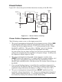
Power Failure ...................................................................................... 135
Power Failure Sequence of Events ................................................ 135
Multiple Power-Line Fluctuations ................................................. 136
Recommended Power-Failure Routine ........................................... 137
Holdup Time .................................................................................. 138
Schematics
vi s Table of Contents
BL1500
ABOUT THIS MANUAL
This manual provides instructions for installing, testing, configuring, and
interconnecting any of the Dynamic C programmable controllers in the
BL1500 series.
The term BL1500 will be used generically throughout this manual when
referring to any controller in the BL1500 series. Where information applies
to a specific controller, the model number will be specified. Models currently covered by this manual include the BL1500, BL1510, and BL1520.
Instructions to get started using Dynamic C software programming functions as well as complete C and Dynamic C references and programming
resources are referenced when necessary.
Assumptions
Assumptions are made regarding the user's knowledge and experience in
the following areas:
Ability to design and engineer a target system that a BL1500 will
control.
Understanding of the basics of operating a software program and
editing files under Windows on a PC.
Knowledge of the basics of C programming.
$
For a full treatment of C, refer to the following texts:
The C Programming Language by Kernighan and Ritchie
C: A Reference Manual by Harbison and Steel
Knowledge of basic Z80 assembly language and architecture.
$
BL1500
For documentation from Zilog, refer to the following texts:
Z180 MPU User's Manual
Z180 Serial Communication Controllers
Z80 Microprocessor Family User's Manual
About This Manual s vii
Acronyms
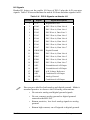
Table 1 lists and defines the acronyms that may be used in this manual.
Table 1. Acronyms
Acronym
Meaning
EPROM
Erasable Programmable Read-Only Memory
EEPROM
Electronically Erasable Programmable Read-Only Memory
LCD
Liquid Crystal Display
LED
Light-Emitting Diode
NMI
Nonmaskable Interrupt
PIO
Parallel Input/Output Circuit
(Individually Programmable Input/Output)
PRT
Programmable Reload Timer
RAM
Random Access Memory
RTC
Real-Time Clock
SIB
Serial Interface Board
SRAM
Static Random Access Memory
UART
Universal Asynchronous Receiver Transmitter
Icons
Table 2 displays and defines icons that may be used in this manual.
Table 2. Icons
Icon
$
(
Meaning
Meaning
Refer to or see
!
Note
Please contact
7LS
Tip
Caution
FD
Icon
High Voltage
Factory Default
viii s About This Manual
BL1500
Conventions
Table 3 lists and defines the typographic conventions that may be used in
this manual.
Table 3. Typographic Conventions
Example
Description
while
Courier font (bold) indicates a program, a fragment of a
program, or a Dynamic C keyword or phrase.
// IN-01…
Program comments are written in Courier font, plain face.
Italics
Indicates that something should be typed instead of the
italicized words (e.g., in place of filename, type a file’s
name).
Edit
Sans serif font (bold) signifies a menu or menu selection.
...
An ellipsis indicates that (1) irrelevant program text is
omitted for brevity or that (2) preceding program text may
be repeated indefinitely.
[ ]
Brackets in a C function’s definition or program segment
indicate that the enclosed directive is optional.
< >
Angle brackets occasionally enclose classes of terms.
a | b | c
A vertical bar indicates that a choice should be made from
among the items listed.
A black square indicates
pin 1 of all headers.
Pin 1
J1
Pin Number 1
Measurements
All diagram and graphic measurements are in inches followed by millimeters enclosed in parenthesis.
BL1500
About This Manual s ix
x s About This Manual
BL1500
CHAPTER 1:
OVERVIEW
Chapter 1 provides an overview and brief description of the BL1500
features, options, and optional upgrades.
BL1500
Overview s 11
Overview
Each BL1500 controller is a small, low-cost board that is easily programmed
using Dynamic C. Moreover, each controller offers impressive processing
power for a wide variety of control applications. Despite its small size, a
BL1500 can accommodate large, real-time multitasking programs.
Real-time programs can be developed on any of the BL1500 controllers in
the target system without the need for expensive in-circuit emulators or
logic analyzers.
All BL1500s allow for protecting data in static RAM and the real-time
clocks contents with an external backup battery (2.5 V to 4.25 V DC).
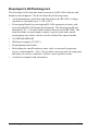
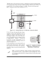
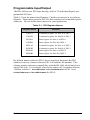
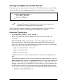
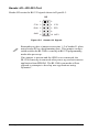
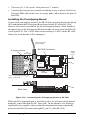
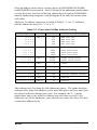
Top View
U1
J1
U3
Reg.
Z180
Y1
U2
PIO 1
H1
Y2
R9
U9
JP1
JP2
RP1
Flash EPROM
H3
U7
U4
U5
PIO 2
U6
R10
U8
R11
R13
R12
R14
U15
U16
A/DC
U13
H2
U14
RTC
U12
U11
Super.
RAM
U10
RS-232
Bottom View
Figure 1-1. BL1500 Board Layout
12 s Overview
BL1500
Features
BL1500
Two Zilog PIO ICs for parallel or bit-oriented digital I/O, 26 total
digital I/O lines plus handshake lines
Socket for up to 256K flash EPROM
Power supervisor IC consisting of watchdog timer, power-fail reset,
and RAM backup-battery switchover
Linear voltage regulator (5 V)
RS-232 serial channel
RS-485 serial channel
Serial Interface Board 2 programming port
Connection for external backup battery (2.5 V to 4.25 V DC) on pin
21 of header H3
Keypad and LCD interface
A real-time clock (RTC), which provides time and date functions and
a 31-byte scratchpad RAM. The RTC reserves two digital-I/O lines,
leaving 24 I/O lines for an applications use.
SRAM (128K)
Four-channel, 12-bit A/D converter. Two channels have onboard,
user-defined signal conditioning, and the other two are unconditioned.
BL1510
All features of the BL1500 except RTC
Two additional PIO lines
SRAM (32K)
BL1520
All features of the BL1500 except RTC and 12-bit A/D converter.
Two additional PIO lines
SRAM (32K)
$
BL1500
Appendix B, Specifications, provides a complete list and
description of BL1500 specifications.
Overview s 13
Options and Upgrades
Serial Interface Board 2 (SIB2) allows programming through the special
programming port, leaving both serial channels available for
applications.
128K or 256K flash EPROM can be factory installed.
128K EPROM.
Real-time clock provides time and date functions and a 31-byte
scratchpad RAM. The RTC reserves two digital-I/O lines, leaving 24
I/O lines for use by the application. This feature is standard on the
BL1500, but can be added to the BL1510 and BL1520 models.
Software Development and Evaluation Tools
Software for the BL1500 is developed using Dynamic C, Z-Worlds real-time
C language development system. Dynamic C for the BL1500 runs under
Windows on a PC.
When a program compiles, the host PC downloads the executable code, via
the BL1500s RS-232 port, directly to the onboard flash EPROM. This
feature allows fast in-target development and debugging.
Another method for downloading programs from a host PC to a BL1500 is
via a Z-World Serial Interface Board 2. By using the optional SIB2, the RS232 port is left free for other applications.
The BL1500 supports up to 256K of electronically re-programmable flash
EPROM. Flash EPROM allows programs to be downloaded into nonvolatile memory without using an EPROM burner.
$
Z-Worlds Dynamic C reference manuals provide complete
software function descriptions and programming instructions.
14 s Overview
BL1500
CHAPTER 2:
GETTING STARTED
Chapter 2 provides instructions for connecting the BL1500 to a host PC
and running a sample program. Sections include the following topics:
Developers Kit Packing List
Connecting the Prototyping Board to the BL1500
Connecting the BL1500 to a Host PC
Establishing Communication
Running a Sample Program
BL1500
Getting Started s 15
Developers Kit Packing List
The Developers Kit includes items necessary for BL1500 software and
hardware development. The kit includes the following items.
An aluminum base plate/heat sink that allows the BL1500s voltage
regulator to dissipate up to 3.5 W at 50°C.
Prototyping Board for prototyping BL1500 expansion circuits, and
powering the BL1500 during development. The Prototyping Board
measures 2.25 × 2.0 inches and connects directly to the BL1500. The
board includes several sample circuits, a power jack, and a small
prototyping area where circuits can be soldered for special needs.
A 128K flash EPROM.
Wall power supply (12 V DC).
Programming serial cable.
Miscellaneous small hardware parts such as assorted connectors,
screws, and standoffs. Also, 26-pin cable connector and 20 crimp pins
that may be used to construct a cable to meet specific needs.
A reference manual with schematics.
16 s Getting Started
BL1500
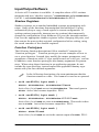
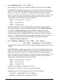
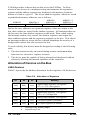
Installing Flash EPROM
If an EPROM is not already installed, install the flash EPROM from the
Developers Kit in socket U6 on the BL1500 shown in Figure 2-1. Make
sure the jumpers on headers JP1 and JP2 are set as shown in Figure 2-1.
3
RP1
Flash EPROM
2 1
JP1
JP2
U6
H3
Figure 2-1. Flash EPROM Installation and Jumper Settings
BL1500
Getting Started s 17
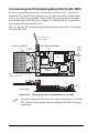
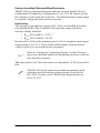
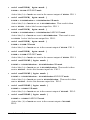
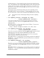
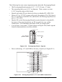
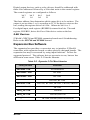
Connecting the Prototyping Board to the BL1500
The Prototyping Board connects to the top of the BL1500. The 26-pin
header (H3) on the BL1500 plugs into the socket strip (H1) on the underside of the Prototyping Board. Most of the Prototyping Board extends
beyond the edge of the BL1500. Figure 2-2 illustrates how to attach the
Prototyping Board to the BL1500.
Pin 1 of header H1 on the Prototyping Board must match pin 1 of header
H3 on the BL1500.
from wall mount
power supply
BL1500 Controller
Prototyping Board
Serial
Cable
to PC
DC
Input Jack
U1
Z180
Y1
U2
Super
Cap.
J1
U3
Reg.
PIO 1
H2
Y2
Buzzer
JP1
JP2
RP1
U6
H3
H1 Pin 1 of Prototyping Board
H3 Pin 1 of BL1500
U4
U9
PIO 2
Flash
EPROM
Top View
Prototyping Board
Side View
BL1500 Controller Board mounted on Baseplate
Figure 2-2. Prototyping Board Attachment to BL1500
!
The Prototyping Board does not require jumpers on its header
H2. Remove the jumpers that are shipped with the Prototyping Board.
18 s Getting Started
BL1500
The Prototyping Board supplies power to the BL1500. Plug the power
supply into the wall and connect it to the direct current input jack on the
Prototyping Board. The BL1500 is now ready for programming.
$
Refer to Appendix D, Prototyping Board, for a full
description and additional information.
When using the Prototyping Board during software development, power
(9 V to 12 V DC) comes through the direct current input jack of the Prototyping Board. In the absence of this board (for example, when you have
completed system development), apply power to pin 25 of header H3.
Always connect the Prototyping Board as shown in Figure 2-2.
Joining the board any other way could damage the BL1500s
components.
BL1500
Getting Started s 19
Connecting the BL1500 to a Host PC
The BL1500 can be connected to a host PC via the RS-232 port or via a
SIB2. Although the ideal development method is with a SIB2, the RS-232
port is the BL1500s onboard development serial port. When a SIB2 is
used, the RS-232 port is available during development to compile and
debug a program.
BL1500 connectors are not polarized or keyed. Carefully observe connector orientation and pin alignment before making a connection and before
applying power.
!
All diagrams in this manual illustrate pin 1 of each connector as
a solid black square.
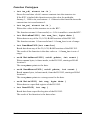
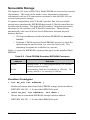
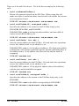
Development Using the RS-232 Port
Using the programming cable provided in the Developers Kit, connect the
BL1500 to a host PC with the following steps. Figure 2-3 illustrates the
connection between the BL1500 and the host PC.
SIB2 Programming Port
1
U3
J1
1
Serial cable
to PC
Z180
H2
Figure 2-3. RS-232 Programming Mode
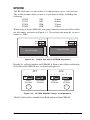
1. Disconnect power source to the BL1500.
2. Connect the RS-232 cable between the host PCs COM port and header
H2 of the BL1500. Be careful to match the arrow on the connector to
pin 1 of header H2.
3. Connect a jumper between pins 1 and 2 of header J1 (the SIB2 port).
4.
Reconnect power source.
The BL1500 is now ready for programming through the RS-232 port.
20 s Getting Started
BL1500
Developing with Optional SIB2
Z-Worlds SIB2 is an interface adapter useful for BL1500 software development. Contained in an ABS plastic enclosure, the SIB2 is rugged and
reliable. Since the SIB2 permits the BL1500 to communicate with Dynamic C
via the Z180s rarely used clocked serial I/O (CSI/O) port, the BL1500s
serial port is freed up. The serial port can then be used by an application.
The SIB automatically selects its RS-232 baud rate to match certain communication rates established by the host PC through Dynamic C. However,
the hosts communication baud rate is determined only on the first communication after reset. To change baud rates, first change the baud rate
through the Dynamic C Serial option in the OPTIONS menu, then reset the
target BL1500 (also resets the SIB2), then select Reset Target or <Ctrl Y)>
in Dynamic C. The SIB2 automatically matches the baud rate of the host
PC at 9600 bps, 19,200 bps, or 57,600 bps.
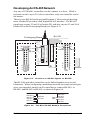
Follow these steps to connect a SIB to a host PC.
1. Disconnect power to the BL1500 if connected.
2. Connect the 6-conductor RJ-12 cable from the PCs COM port to the SIB2.
3. Connect the SIB2s small ribbon cable to header J1 on the BL1500 as
shown in Figure 2-4. Match the arrow on the SIB2 connector to pin 1 of
header J1.
JP1
JP2
U9
U4
Never connect or disconnect
the SIB2 when the power is
being applied.
H1
Pin 1
J1
Z180
H2
U3
To Host PC
Marked
Conductor
to Pin 1
Figure 2-4. Serial Interface Board 2 Connection to BL1500
4. Reconnect the power supply to the BL1500.
The system is now ready for programming through the SIB2.
BL1500
Getting Started s 21
Establishing Communication
After hardware is connected, communication can be established between a
host PC and the BL1500.
Communication is established by double-clicking the Dynamic C icon to
start the software.
!
Communication with the BL1500 is attempted each time
Dynamic C starts.
When communication is established, no error messages are displayed.
$
See Appendix A, Troubleshooting, if an error message such
as Target Not Responding or Communication Error appears.
After making any necessary changes to establish communication between
the host PC and the BL1500, use the Dynamic C shortcut <Ctrl Y> to reset
the controller and initialize communication.
Running a Sample Program
The following steps describe how to run a sample program to determine if
hardware connections are correctly established.
1. Open the sample program MGDEMORT.C located in the Dynamic C
SAMPLES\BL14_15 subdirectory.
2. Compile the program by pressing <F3> or by choosing Compile from
the COMPILE menu. Dynamic C compiles and downloads the program
into the BL1500s flash memory.
During compilation, Dynamic C rapidly displays several messages in
the compiling window. This condition is normal.
3. To run the program, press <F9>, or choose Run from the RUN menu.
5. To halt the program execution, press <Ctrl Z>.
6. To restart program execution, press <F9>.
22 s Getting Started
BL1500
CHAPTER 3:
SUBSYSTEMS
Chapter 3 discusses the following topics.
Interface Overview
PIOs (Programmable I/O ICs)
Power-Supervisor Integrated Circuit
Serial Communication Ports
Analog-to-Digital Converter
Real-Time Clock
BL1500
Subsystems s 23
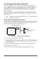
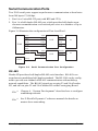
Interface Overview
This section describes the various interfaces of the BL1500. Figure 3-1
provides a block diagram reference of the available interfaces.
BL1500 Series
+5 V
Z180
Regulator
Serial
RS-232
Serial
RS-485
DCIN
Timer
Reset
A/D
Converter
EPROM or
flash
EPROM
VRAM
Analog Inputs
691
Supervisor
RAM
External Battery
VBAT
RTC
PIO1
Port A
Digital I/O
Port B
+5 V
PIO2
Port A
Digital I/O
Port B
Figure 3-1. BL1500 Interface Diagram
24 s Subsystems
BL1500
Programmable Input/Output ICs (PIOs)
The BL1500 uses two Zilog PIO ICs to provide digital I/O signals:
(1) PIO 1, U2, (2) and PIO 2, U9.
Each PIO has two 8-bit, parallel, programmable I/O ports called Port A
and Port B. Each line of a port can serve as an input or output in different modes.
The signal nomenclature identifies the various ports and pins of the PIOs
discussed in this section.
P1A0P1A7 are data lines 0 through 7 of PIO 1 Port A.
P2B7 is data line 7 of PIO 2 Port B.
!
Drivers for PIO 1 do not indicate a PIO number.
Drivers for PIO 2 do indicate a PIO number.
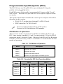
PIO Modes of Operation
There are four modes of operation for PIO Port A and Port B. Port A of
PIO 1 may operate in modes 0, 1, and 3, but not in mode 2. Port A of PIO 2
operates in mode 3, bitwise I/O only. Likewise, both PIOs of Port B operate
in mode 3, bitwise I/O only. Table 3-1 and Table 3-2 list and define the four
modes of operation.
Table 3-1. PIO Modes of Operation
Mode
Description
Mode 0
Strobed byte output
Mode 1
Strobed byte input
Mode 2
Bidirectional data transfer
Mode 3
Bitwise I/O, input/output selectable per bit
Table 3-2. Permissible PIO Port Operating Modes
PIO 1
PIO 2
Mode
BL1500
Port A
Port B
Port A
Port B
Mode 0
Yes
No
No
No
Mode 1
Yes
No
No
No
Mode 2
No
No
No
No
Mode 3
Yes
Yes
Yes
Yes
Subsystems s 25
The PIO lines can also detect transitions interrupting the microprocessor in
various ways. Although each port has two handshake lines, the only
usable handshake lines for Port A of PIO 1 appear on header H3.
Port A lines have TTL-compatible logic levels. In addition to being TTLcompatible, Port B lines can supply up to 1.5 mA at 1.5 V to drive Darlington transistors. For either port, you may need to add current-limiting resistors, noise filters, or transient voltage suppression circuitry, depending on
the application.
The impedance of a PIO line is approximately 80 Ω for sinking current and
160 Ω for sourcing current. Do not apply negative voltages (voltages
below ground) or voltages above VCC (+5 V) to either PIO.
PIO 1
Four lines of PIO 1
Port B are preassigned.
Figure 3-2 illustrates
each line location and
Table 3-3 lists and defines the signals and
their function for specific pins.
D0
D1
D2
D3
D4
D5
D6
D7
D0
D1
D2
D3
D4
D5
D6
D7
PA7
PA6
PA5
PA4
PA3
PA2
PA1
PA0
PIO 1
U2
P1A7
P1A6
P1A5
P1A4
P1A3
P1A2
P1A1
P1A0
ARDY
ARDY /ASTB
/ASTB
P1B7
PB7 P1B6
PB6 P1B5
PB5 P1B4
PB4 RTCCLK
PB3 RTCDAT
PB2 EN485
PB1 /RTCRST
PB0
NC
BRDY GND
/BSTB
Figure 3-2. PIO 1 Line Map
Table 3-3. PIO 1 Preassigned Pins
PIO 1 Port
Pin Signal
Pin Function
P1B3
RTCCLK
RTC serial clock
P1B2
RTCDAT
RTC serial data
P1B1
EN485
RS-485 transmit enable
P1B0
/RTCRST
RTC reset
26 s Subsystems
BL1500
H3 Signals
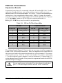
Header H3 brings out the usable I/O lines of PIO 1 plus several other miscellaneous signals. Table 3-4 lists and defines the usable I/O lines and other
signals for header H3.
Table 3-4. PIO 1 Signals on Header H3
H3 Pin
!
BL1500
Signal
Signal Description
1
+5 V
Regulated Power
2
P1A0
PIO 1 Port A, Data Line 0
3
P1A1
PIO 1 Port A, Data Line 1
4
P1A2
PIO 1 Port A, Data Line 2
5
P1A3
PIO 1 Port A, Data Line 3
6
P1A4
PIO 1 Port A, Data Line 4
7
P1A5
PIO 1 Port A, Data Line 5
8
P1A6
PIO 1 Port A, Data Line 6
9
P1A7
PIO 1 Port A, Data Line 7
10
GROUND
Digital Ground
11
ARDY
PIO 1 Port A Handshake Line
12
/ASTB
PIO 1 Port A Handshake Line
13
P1B7
PIO 1 Port B, Data Line 7
14
P1B6
PIO 1 Port B, Data Line 6
15
P1B5
PIO 1 Port B, Data Line 5
16
P1B4
PIO 1 Port B, Data Line 4
17
RTCCLK
Real-Time Clock Control Lines
18
RTCDAT
Real-Time Clock Data Line
19
/RESET
Reset Signal
20
GROUND
Digital Ground
21
VBAT
External Battery Input
22
GROUND
Digital Ground
23
RS-485+
RS-485+
24
RS-485-
RS-485-
25
DCIN
Unregulated Voltage Input
26
GROUND
Digital Input
Since the BL1510 and BL1520 do not have a real-time clock
(RTC), PIO 2 lines P1B3 and P1B2 are available for use.
Subsystems s 27
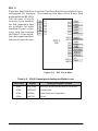
PIO 2
Eight data lines from Port A and four lines from Port B are available for general-purpose I/O functions. The remaining four lines of Port B have been
preassigned to the BL1500s
A/D converter. If an A/D
D0 D0
P2A7
converter is not installed,
PA7 P2A6
D1 D1
PA6
the four remaining lines
D2 D2
P2A5
PA5 P2A4
D3 D3
are available for other
PA4 P2A3
D4 D4
PA3 P2A2
functions. Figure 3-3 illusD5 D5
PA2 P2A1
D6 D6
trates each line location
PA1 P2A0
D7 D7
and Table 3-5 lists and dePA0
fines the signals and their
/ADCS
ARDY GND
function for specific pins.
/ASTB
PIO 2
U9
PB7
PB6
PB5
PB4
PB3
PB2
PB1
PB0
P2B7
P2B6
P2B5
P2B4
EOCNMI
ADDOUT
ADDIN
ADCLK
NC
BRDY GND
/BSTB
Figure 3-3. PIO 2 Line Map
Table 3-5. PIO 2 Preassigned Analog-to-Digital Lines
PIO 2 Port
Signal
Analog-to-Digital Function
P2B3
EOCNMI
End of Conversion and Power Fail Sense
P2B2
ADDOUT
Output Data
P2B1
ADDIN
Input Data and Commands
P2B0
ADCLK
Clock
28 s Subsystems
BL1500
H1 Signals
Header H1 brings out the usable I/O lines of PIO 2 plus the A/D converter
signals. Table 3-6 lists and defines the usable I/O lines and other signals for H1.
Table 3-6. PIO 2 Signals on Header H1
H1 Pin
!
Signal
Signal Description
1
+5 V
Regulated Power
2
P2A0
PIO 2 Port A, Data Line 0
3
P2A1
PIO 2 Port A, Data Line 1
4
P2A2
PIO 2Port A, Data Line 2
5
P2A3
PIO 2 Port A, Data Line 3
6
P2A4
PIO 2 Port A, Data Line 4
7
P2A5
PIO 2 Port A, Data Line 5
8
P2A6
PIO 2 Port A, Data Line 6
9
P2A7
PIO 2 Port A, Data Line 7
10
GROUND
Digital Ground
11
P2B4
PIO 2 Port A, Data Line 4
12
P2B5
PIO 2 Port A, Data Line 5
13
P2B6
PIO 2 Port A, Data Line 6
14
P2B7
PIO 2 Port A, Data Line 7
15
AD2
Unconditioned A/D Input
16
AD3
Unconditioned A/D Input
17
VREF
A/D Voltage Reference
18
AD1
Conditioned A/D Input
19
AGND
Analog Ground
20
AD0
Conditioned A/D Input
Pins are provided for both analog and digital ground. Make it
standard practice to observe the following conventions.
Do not mix analog and digital ground signals.
Do not connect analog ground to digital ground
external to the BL1500.
Return sensitive, low-level analog signals to analog
ground.
Return high current, on-off signals to digital ground.
BL1500
Subsystems s 29
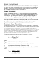
Power-Supervisor Integrated Circuit
The ADM691 power-supervisor IC is a key component that helps a system
survive power fluctuations and power outages. Several vital services
provided by the power supervisor are described below.
Power-on reset
The supervisor IC generates the power-on reset for the BL1500 by holding
/RESET low until the IC senses that VCC has risen above the reset
threshold (~4.65 V) and the battery voltage (2.5 V to 4.25 V DC). When
VCC falls below the threshold, the supervisor IC disables the RAM to
prevent spurious writing of data.
RAM protection
The power supervisor IC gates the decoded RAM-select line (/RAMSEL)
to the RAMs chip-enable line (/RAMCE) whenever VCC is above the reset
threshold and VBAT. When VCC falls below the threshold, the ADM691
de-asserts /RAMCE to prevent spurious writing to the RAM.
Watchdog timer
The watchdog timer cannot be disabled. The watchdog timer guards
against system or software faults. If an application does not hit the
watchdog timer at least every 1.0 seconds, the watchdog timer resets the
Z180. The supervisors watchdog output (/WDO) connects to the Z180s
/INT1 interrupt line. /WDO is at logic zero level after a watchdog reset and
at logic 1 after a power-on reset.
!
To hit the watchdog timer, make a call to the library function
hitwd. This call makes a dummy one-byte DMA transfer via
DMA channel 1, which activates the DMA-end signal,
/TEND1, hitting the watchdog timer.
Nonmaskable interrupt
The ADM691 generates a nonmaskable interrupt (/NMI) from its power-fail
output (/PFO) for the microprocessor if the unregulated DC input (normally
9 V to 12 V DC) falls below 7.9 V. This gives the BL1500 advanced warning
of an impending power failure, which allows it to execute shutdown routines. The voltage divider (R1 and R15) determines the power-fail voltage
level.
R16 introduces approximately 830 mV of hysteresis into the supervisor ICs
sensing of the raw DC, preventing noise on DCIN from generating repeated
interrupts when the input voltage is low. /NMI also connects to Port B
(bit 3) of PIO 2 (via U7B) to allow your software to monitor the /NMI line
after the nonmaskable interrupt, and to recover from temporary low-input
voltage conditions or brownouts.
30 s Subsystems
BL1500
Backup-battery switchover
The ADM691 switches the RAM over to battery power if VCC falls below
the battery voltage VBAT (2.5 V to 4.25 V DC).
!
BL1500
Provide an external backup battery to take advantage of the
backup battery switchover. Resistor R17 prevents false resets
when changing the battery with the power on.
Subsystems s 31
Serial Communication Ports
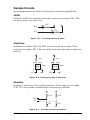
Two Z180 serial ports support asynchronous communication at baud rates
from 300 bps to 57,600 bps.
1. Port 0 is a 5-wire RS-232 port (with RTS and CTS).
2. Port 1 is a half-duplex RS-485 port, which provides half-duplex asynchronous communication over twisted pair wires to a distance of up to
4 kilometers.
Figure 3-4 illustrates the configuration of Port 0 and Port 1.
TXD0
TXD0
/TDAT
3
RXD0
RXD0
/RDAT
5
U10
Z180
H2
/RTS0
/RTS0
RTS
6
/CTS0
/CTS0
CTS
4
TXD1
RXD1
TXD1
RXD1
RS485+ 23
U13
RS485– 24
H3
EN485
PIO 1
(P1B1)
Figure 3-4. Serial Communication Port Configuration
RS-485
Header H3 provides a half-duplex RS-485 serial interface. RS-485 is an
asynchronous multidrop half-duplex standard. The BL1500 can be configured to provide one channel of RS-485 communication with multidrop
network capabilities. The RS-485 signals are on pins 23 and 24 of header
H3, and also on pins 23 and 24 of header H2 on the Prototyping Board.
$
Chapter 4, System Development describes how to configure
a multidrop network.
$
See Z-Worlds Dynamic C reference manuals for details on
master-slave networking.
32 s Subsystems
BL1500
RS-232 and Programming Ports
Header H2 provides a 5-wire RS-232 interface that is used for programming.
However, the BL1500 can be programmed without using the RS-232 port by
using the Serial Interface Board 2 (SIB2). By connecting a SIB2 to header
J1, the Z180 port can be used for programming and debugging, leaving the
RS-232 interface available to an application during development.
Z-World has RS-232 support libraries for the BL1500s Z180 Port 0. Support for serial communication includes the following functions.
Initializing the serial ports.
Monitoring and reading a private circular receive buffer.
Monitoring and writing to a private circular transmit buffer.
CTS (clear to send) and RTS (request to send) control.
XMODEM protocol for downloading and uploading data.
A modem option.
An echo option.
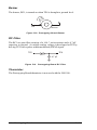
Modem Communication
Modems and telephone lines allow RS-232 communication across great distances. A modem automatically scans character streams that are read from
the receive buffer for modem commands. The RS-232 library supports communication with a Hayes Smart Modem or compatible modem. If the modem
used is not truly compatible, you
Modem
BL1500
must tie the CTS, RTS, and DTR lines
Side
Side
on the modem side together. Additionally, the CTS and RTS lines on
RX
RX
the BL1500 side also have to be tied
TX
TX
together. A NULL connection is also
GND
GND
required for the TX and RX lines.
RTS
RTS
However, a commercial NULL modem
CTS
CTS
already has its CTS and RTS lines
DTR
tied together on both sides.
Figure 3-5 illustrates the connections
between a BL1500 and a modem.
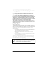
Figure 3-5. Connections Between
Controller and Modem
The BL1500 supports the XMODEM protocol for downloading and
uploading data. Currently, the library supports downloading an array of
data in multiples of 128 bytes.
Uploaded data are written to a specified area in RAM. The targeted writing
area should not conflict with the current resident program or data.
Character echo is automatically suspended during XMODEM transfer.
$
BL1500
See Z-Worlds Dynamic C reference manuals for details on
software functions for modem communication.
Subsystems s 33
Analog-to-Digital Converter
The optional BL1500 A/D converter is a 12-bit, serial-I/O, switchedcapacitor, successive-approximation converter that can monitor temperature, measure position, or sense other types of analog signals. In response
to commands received from the Z180 via PIO 2, the A/D converters internal
multiplexer samples and converts one input channel at a time.
Based on the A/D converters minimum conversion period, the maximum
data conversion rate is approximately 5,000 conversions per second.
Z-World cannot guarantee this level of performance because application
programming can have a major affect on the conversion rate.
The A/D converter IC provides four channels of 12-bit analog-to-digital
conversion. Two of the channels have op-amps for signal conditioning
and two are unconditioned. The input range for the unconditioned channels is 0 V to 2.5 V. The two unconditioned channels also have onboard
sensor-excitation resistors.
A dual op-amp (U16) buffers the two analog inputs received over signal
lines AD0 and AD1 of header H1. The outputs of U16 go to the first two
inputs of the A/D converters (U15) eleven inputs. The two unconditioned
signals AD2 and AD3 go through anti-latchup resistors R5 and R7 to the
next two A/D inputs.
Extra Conversion
The A/D converter sends converted data out serially and receives commands serially. During each serial-clock cycle, the chip shifts in one
command bit and shifts out one data bit. This combined shifting accounts
for the devices behavior of returning a previous data reading automatically
each time it accepts a conversion or configuration command.
The A/D converter communicates with the Z180 via data-input line ADDIN,
the data-output line ADDOUT, the clock line ADCLK, the end-of-conversion line EOC, and the IC-select line /ADCS.
EOC goes to a logic 0 level during conversion, returning to 1 when the
conversion is complete. Following the conversion period, the A/D converter shifts the resulting data one bit at a time over ADDOUT. Also, during each shift-clock period, the converter shifts in one bit of a command
word into the converter over ADDIN. This command word specifies the
converters next operation. The PIOs ARDY line drives /ADCS. This line
goes from a logic 1 to 0 during power-on initialization as a result of
putting Port A into mode 3 operation. This transition is necessary for the
chip to function properly. After transition, the line is left low.
34 s Subsystems
BL1500
EOC comes in over PIO Port B data line 3 (P2B3), which also senses
/NMI through the logic gate U7. (/NMI and EOC are not at a logic 0 level
at the same time, and the driver software can distinguish between them in
context.)
Library routines take care of all the low-level details of communication with
the A/D converter automatically.
!
The protocol for controlling the serial A/D converter is complex. Z-World strongly recommends using existing Dynamic C
library functions to control the converter instead of writing
your own functions.
Voltage Reference
The A/D converters two reference inputs REF- and REF+ establish the
voltage limits for analog inputs that produce the maximum and minimum
conversion values. Inputs higher than REF+ return the maximum conversion value, and inputs less than REF- return the minimum conversion
value. The A/D converter has no out-of-range signal. Software will not be
able to distinguish between an input that is exactly at either limit of the
voltage range and an input that exceeds the limits.
Data Conversion
The two conditioned inputs measure input signals over either a bipolar or a
unipolar voltage range. In either case, the operational amplifiers gain and
bias resistors scale the signal ranges to conform to the 0 V to 2.5 V input
range of the A/D converter. The inverting configuration of the op-amps
means that the maximum input voltage results in a minimum input voltage
at the converter.
The A/D converter determines a 12-bit digital value representing the
converted value of the input voltage. An input voltage at the A/D converter (equal to 0 V) converts to all zeros, and an input at 2.5 V converts to
all ones. Dynamic C functions return 16-bit sign-extended values. The
functions return a reading appropriate to the unipolar or bipolar signals
being measured, based on the arguments supplied to the function.
Limitations on Output Range
In actual practice, the op-amp outputs can only approach ground (0 V) but
cannot actually reach it. The output low-voltage limit is about 10 mV to 20 mV.
The practical effect of this limitation is that approximately 0.4%0.8% of the
upper end of the input-signal range is unusable. For example, if the input
signal ranges from 0 V to 10 V, the maximum useful input voltage is 9.92 V
to 9.96 V.
BL1500
Subsystems s 35
Low-Pass Filter
The 0.01 µF feedback capacitors (C20 and C21) in the amplifiers circuits
transform the amplifiers into low-pass filters. These filters attenuate any
high-frequency noise that may be present in a signal. The filter characteristics depend on the resistors selected. The 3 dB corner frequency is
1
(3-1)
.
f 3db =
2π × R g × 0.01 µF
For the above case with a gain of 0.25 using a 1% feedback resistor of
2370 Ω, the 3 dB corner frequency is 6715 kHz.
Internal Test Voltages
By addressing virtual channels in the A/D converter, Dynamic C routines
can obtain internal test voltages from the A/D converter. However, these
readings measure VREF+ and VREF- with respect to VREF and GND so that
the resulting conversions are all 0s or all 1s.
Drift
The AD680JT voltage reference exhibits a voltage drift of 10 ppm/°C (typ)
to 30 ppm/°C (max). This drift corresponds to 25 µV/°C to 75 µV/°C, or
1.75 mV to 5.25 mV over the temperature range of 0°C to 70°C.
The LMC662C operational amplifier exhibits an offset-voltage drift of
1.3 µV/°C (typ), or 910 µV over the temperature range.
A greater contribution to overall drift arises from differences in the
temperature coefficients of the user-installed gain and bias resistors and
the fixed 10 kΩ resistors R21R24. Resistors R21R24 have temperature
coefficients of ±200 ppm/°C. Because they are small, surface-mount
resistors, and are close to each other, they are always at essentially the
same temperature and their temperature deviations track closely.
Absolute and Ratiometric Modes
The A/D converter can operate in either an absolute or a ratiometric mode.
In absolute mode, the A/D converter compares the input signal
against an accurate, stable onboard reference. The onboard
voltage-reference is an AD680JT, which has a drift specification of
10 ppm/°C (typical).
In ratiometric mode, both the reference voltage and the voltage for
the sample are connected to the same power supply. Because the
reference voltage and the sample voltage experience the same
power supply fluctuations, the ratiometric mode minimizes errors
in certain types of measurements, specifically those measurements where the BL1500 has to supply an excitation voltage to a
bridge or transducer.
36 s Subsystems
BL1500
The BL1500s A/D converter is factory configured to operate in the absoluteconversion mode using a precision onboard voltage reference (an AD680, U4,
or an LM385, U5) as shown in Figure 3-6. REF- is hard-wired to ground.
REF+ connects to one of two sources of 2.5 V.
+5 V
R19
10 kΩ
(Optional)
+5ANA
R9
2.2 kΩ
AD680JT
In
VREF
Out
GND
LM385-2.5
C3
0.1 µF
U4
U5
Figure 3-6. Analog Reference in Absolute Conversion Mode
!
BL1500
U9
U4
PIO 2
U5
R10
For the ratiometric-conversion mode, you
need to know the resistor values used in
the op-amp circuit before you can determine the values you need to install for R9
and R10.
H1
R9
U4 (or U5) may be removed and voltagedividing resistors R9 and R10 may be
added to change the BL1500 to the
ratiometric mode. The axial-lead resistors at R9 and R10 form a voltage divider
to supply REF+. Figure 3-7 shows the
locations of the components to be
changed, and the resulting circuit is
shown in Figure 3-8.
Figure 3-7. Location of Analog
Reference Components for
Ratiometric Conversion
REF+ is also the reference voltage for the op-amps used with
A/D channels 0 and 1. The resistors of the op-amp bias circuit
will interact with the R9/R10 voltage divider to affect the actual
value or REF+.
Subsystems s 37
+5 V
R19
10 kΩ
+5ANA
R9
2.2 kΩ
VREF
R10
2.2 kΩ
C3
0.1 µF
Figure 3-8. Analog Reference in Ratiometric Conversion Mode
Bipolar or Unipolar Conditioned Inputs
The two conditioned inputs can be used to measure bipolar or unipolar
signals. The inputs for the two conditioned channels, AD0 and AD1, are
pins 18 and 20 of header H1. The unconditioned inputs, AD2 and AD3, use
pins 15 and 16 of header H1.
R9
Signals from sensors connected to AD0 and AD1 of H1 go to the inverting
input of one of the two op-amps in U16. U16s op-amps operate in the
inverting configuration. User-selectable
resistors R11 through R14 set the gain
H1
and bias voltages of the amplifiers. The
10 kW input and bias resistors (R21
U9
through R24) are fixed. Feedback
U4
U5
PIO 2
capacitors C20 and C21 roll off the highfrequency response of the amplifiers to
attenuate noise.
R13
R11
R10
R12
R14
Figure 3-9. Location of Gain
and Bias Resistors
38 s Subsystems
Figure 3-9 shows the location of the
gain and bias resistors (R11R14) used
to condition the analog input.
BL1500
Factory-Installed Gain and Bias Resistors
The BL1500 is configured with gain and bias resistors installed for the
conditioned A/D channels (configured for 0 V to 10 V DC inputs) so that
the controller works right out of the box. If a different input voltage range
is required, change the gain and bias resistors.
Initial Setup
The op-amps gain and bias resistors, R11R14, are installed in sockets
provided on the BL1500. Each BL1500 controller comes with these
resistors already installed.
RGAIN: R11 and R13 = 2370 Ω
RBIAS,: R12 and R14 = 39.2 kΩ
Resistors R11R14 yield a nominal gain of 0.25 for a unipolar input signal
ranging from 0 V to 10 V. These values differ slightly from theoretical
values to allow for real-world resistor tolerances.
$
Refer to Setting Up Conditioned Inputs on the following
pages for a detailed method of determining the best values for
gain and bias resistors.
The strip sockets on 0.300-inch centers accommodate 1/8 W resistors R11
R14.
!
BL1500
The BL1500 can be ordered in production quantities with
customer-specified surface-mount resistors installed for
R11R14. Contact your Z-World Sales Representative at
(530) 757-3737.
Subsystems s 39
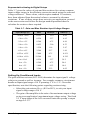
Representative Analog-to-Digital Setups
Table 3-7 gives the values of gain and bias resistors for various common
input-voltage ranges in the absolute-conversion mode using the onboard
voltage reference. These values, which require standard 1% resistors,
have been adjusted from theoretical values to account for tolerance
variations. If one of these setups does not suit your application, proceed
to the next section and follow the design method presented there to
calculate the resistor values required.
Table 3-7. Gain and Bias Resistor Input Voltage Ranges
Input Range (V)
Gain
RGAIN (kΩ)
RBIAS (kΩ)
-10.0 to +10.0
0.125
1.18
8.06
-5.0 to +5.0
0.250
2.37
6.65
-2.5 to +2.5
0.500
4.75
4.99
-2.0 to +2.0
0.625
5.90
4.53
-1.0 to +1.0
1.250
11.8
2.87
-0.5 to +0.5
2.500
23.7
1.69
-0.25 to +0.25
5.000
47.5
0.931
-0.10 to +0.10
12.500
0 to +10.0
0.250
2.37
39.2
0 to +5.0
0.500
4.75
20.0
0 to +2.5
1.000
9.53
10.0
0 to +1.0
2.500
118
23.2
0.392
4.02
Setting Up Conditioned Inputs
The gain and bias resistors (R11R14) determine the input signals voltage
relative to ground as well as its range. For example, assume a circuit must
handle an input signal range of 10 V spanning -5 V to +5 V. Given this
specification, note the following points regarding resistor sizing.
Select the gain resistor, RGAIN (R11 or R13), to suit your input
signal voltage range of 10 V.
The gain of the amplifier is the ratio of its maximum output voltage
swing to an applications maximum input voltage swing. The fixed
2.5 V input range of the A/D converter limits the op-amps output
swings to 2.5 V.
40 s Subsystems
BL1500
Equation (3-2) expresses an amplifiers gain in terms of its input voltage
range, where g is the gain, VINmax is the maximum input voltage, and VINmin
is the minimum input voltage.
g=
(3-2)
The ratio of the user-specified gain resistor R GAIN (R11 or R13) to its
associated fixed input resistor (R21 or R23) determines an amplifiers
gain. For the amplifier in Figure 3-10 with its input resistor fixed at
10 kΩ, the gain is
g=
2.5 V
VINmax − VINmin
R GAIN
10 kΩ
(3-3)
.
Given an input voltage range of 10 V, this gain equation fixes the
amplifiers gain at 0.25, and scales the input signals range properly
down to the op-amps 2.5 V maximum output range. RGAIN must
therefore be 2500 Ω.
C20, C21
0.01 µF
RGAIN
R11, R13
AD0 (H1-20),
AD1 (H1-18)
10 kΩ
–
VR0-,
VR1-
R21,
R23
R22,
R24
VR0+,
VR1+
VREF (H1-17) 10 kΩ
AIN0 (U15-1),
AIN1 (U15-2)
+
RBIAS
R12, R14
Figure 3-10. Gain and Bias Resistors for
Conditioned Analog Inputs
BL1500
Subsystems s 41
Determine Bias Resistor To Center Span
If the op-amp is to servo its output properly around the desired center
voltage, establish the appropriate bias voltage at the op-amps
noninverting input. Select the bias, or offset, resistor RBIAS (R12 or R14) to
position the input voltage range correctly with respect to ground (in this
example, -5 V to +5 V).
Because the value for RGAIN has already been selected, the maximum input
voltage (VINmax) determines the maximum input voltage seen at the amplifiers summing junction (inverting input), circuit nodes VR0- and VR1-. Compute VR0- or VR1- using Equation (3-4).
g
VR0- = VIN max ×
1+ g
.
(3-4)
The bias voltage (VBIAS) must equal its corresponding VRn- for each
op-amp. A voltage divider, comprising a bias resistor RBIAS (R12 or R14)
and a fixed 10 kΩ resistor (R22 or R24), derives this bias voltage (VBIAS =
VR0+ or VR1+) from VREF, the 2.5 V reference voltage. Equation (3-5)
gives RBIAS.
R BIAS =
VBIAS ×10 kΩ
2.5 V - VBIAS
.
(3-5)
The 2.5 V term in the Equation (3-5) denominator is the reference voltage.
The low-impedance voltage reference supplies this voltage when the
BL1500 is in the absolute conversion mode.
When the BL1500 is being used in the ratiometric mode, the optional
resistive divider R9R10 supplies this voltage. But, in this case, the
op-amps bias resistors R12, R22, R14, and R24 load the divider (more
correctly, the bias resistors are, in effect, part of the divider in parallel with
R10). Therefore, first compute values for R12, R22, R14, and R24, assuming
that VREF is 2.5 V. Then compute the required values of R9 and R10 that
derive a reference voltage of 2.5 V while taking into account the resistance
of R12, R22, R14, and R24.
Unipolar Variation
Suppose the input range is 0 V to +10 V instead of -5 V to +5 V. VINmax is
now +10 V, VBIAS becomes 2.0 V, and RBIAS is 40 kΩ.
Choose Best Standard Resistor Values
Calculated values are not always be available as standard resistor values.
In these cases, use the nearest standard resistor value. For example, rather
than 6667 Ω, use 6650 Ω if using one percent resistors, or 6800 Ω if using
5 percent resistors.
42 s Subsystems
BL1500
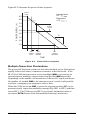
Bracketing Input Range
To be sure of accurately measuring signals at the extremes of an input range,
be aware of the interaction between the 10 kΩ fixed resistors R21R24 and
the other installed resistors R11R14. In the ideal case, if a signal is
measure at the minimum input level, the A/D converters input would be at
the maximum expected value of 2.5 V.
Resistor values vary within their rated tolerance bands. Thus, if the fixed
input resistor is lower than its nominal value, and the installed resistor is
slightly higher than its nominal value, the actual input to the A/D converter
would be greater than 2.5 V. A loss of accuracy then results because the
A/D input would reach its maximum input value before the true signal input
reaches the minimum expected input level.
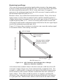
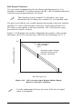
Figure 3-11 shows how variations in tolerance can cause the analog signal
to exceed the limits of the analog converter.
Out of range
2.5
A/D Converter Input (V)
A/D converter's
input-voltage
limit
Op-amp output-voltage
deviation arising from
resistor variations
0
Out of range
10
BL1500 Input (V)
Figure 3-11. A/D Converter Input Ranges Out of Range
Based on Resistor Variation
A deviation from nominal values in the bias network could skew the A/D
converters input voltage away from a theoretically computed value. For
example, a small positive or negative deviation of the bias voltage arising
from variances in the resistive divider would offset the A/D converters
input voltage. This offset would be positive or negative, tracking the
deviations sign, and equal to the bias deviation multiplied by the amplifiers gain plus one. Both of these effects could occur in the same circuit.
BL1500
Subsystems s 43
Pick Proper Tolerance
Use care when compensating for any discovered discrepancies. For
example, if standard 5% resistors are used for R11R14, remember that their
values are spaced approximately 10% apart.
!
The tolerance is plus or minus 5%; therefore, any value
calculated will be within plus or minus 5% of a standard value.
If a gain is too high by just a small amount, then going to the next smallest
standard 5% value could result in a decrease in gain approaching 10%.
The same caveat applies to the bias network. Use 1% resistors to get a
more precise choice of values.
Figure 3-12 illustrates the results of adjusting the resistor values so that
the input to the A/D converter stays within its specified range of 2.5 V.
2.5
A/D Converter Input (V)
A/D converter's
input-voltage
limit
Op-amp output-voltage
deviation arising from
resistor variations
0
10
BL1500 Input (V)
Figure 3-12. A/D converter Input Ranges Within Range
Based on Resistor Variations
!
Use the mathematically derived values if the loss of signal
range is acceptable.
44 s Subsystems
BL1500
Confirm Performance
If measurements are critical, check the setups after installing resistors by
measuring test signals at and near the input-voltage limits. See if the
voltages fall within the A/D converters input range or if loss of accuracy
occurs because of overexcursions at the A/D converters input. Alternatively, measure the resistance of the factory-installed fixed resistors before
selecting and measuring your own resistors.
Fixed resistors can be measured indirectly after being installed by measuring
the voltages at the amplifiers inAIN0 VR1puts and outputs. Using Channel
VR00 as an example, ground the input
R13 AIN1
R11
AD0 at pin 20 of H1. Then measure the voltages at VR0- and the
R14 GND
VR0+ R12
amplifiers output. The voltage test
GND VR1+
points are shown in Figure 3-13,
and their location on the BL1500
Figure 3-13. Voltage Test Points
is shown in Figure 3-9.
Because the currents through the input resistor and the feedback resistor
are essentially identical, the ratio of the voltages across the resistors is
equivalent to the ratio of the resistors. Therefore, the gain is as displayed
in Equation (3-6).
Similarly, again using Channel 0 as an example, measure the voltage of
VREF (pin 17 on header H1) and the voltage at VR0+ (see Figure 3-13).
VOUT - VR0 (3-6)
VR0 Because the current into the op-amp input is negligible, the resistance ratio
of the two resistors in the voltage divider alone determines VR0+. Once
both the value of the installed resistor and the value of VR0+ are known,
compute the value of the fixed resistor in the divider.
gain =
Calibrating the A/D Converter
The inherent component-to-component variations of 5% or 1% resistors
can swamp the 0.25% resolution of the A/D converter. To achieve the
highest accuracy possible, calibrate the BL1500.
The software drivers for the A/D converter provide routines to compute
calibration coefficients (given two reference points) and store them in a
defined location in nonvolatile memory. Each reference point is determined
from the following pair of values:
1. The actual applied test voltage.
2. The raw converted A/D value (a 12-bit integer).
Dynamic C automatically uses these coefficients to correct all subsequent
A/D readings.
BL1500
Subsystems s 45
Dynamic C automatically uses these coefficients to correct all subsequent
A/D readings. Table 3-8 lists the addresses in simulated EEPROM where
the calibration constants are stored.
Table 3-8. A/D Converter Calbration Constants
Address in Simulated EEPROM
A/D Channel
10–15
0
16–21
1
22–27
2
28–33
3
Using Unconditioned Converter Channels
Two additional input channels of the A/D converter (AD2 and AD3) are
available at pins 15 and 16 on header H1. These channels can be accessed
with software by inserting the appropriate channel number in the library
functions that control the A/D converter.
Resistors R0 and R1 (10 kΩ pullup resistors) inside resistor network RN3 are
connected to these two A/D channel inputs to ensure that the inputs do not
float if no input signals are present. These pullup resistors can also be used
as excitation resistors if the sensor or transducer being used needs a resistor
connected to the voltage
+5 V
supply. Each input also has
RN3, pin 2
a 330 Ω series resistor in
10 kΩ
place to guard against latchH1-15
AIN2
up in the A/D converter. This
AD2
U15-3
value is within the 1000 Ω
R5
330 Ω
maximum source driving re+5 V
sistance that the A/D conRN3, pin 1
verter manufacturer specifies
10 kΩ
as being adequate to charge
H1-16
AIN3
the converters internal samAD3
U15-4
R7
ple-and-hold capacitors.
Figure 3-14 illustrates these
additional A/D converter input channels.
46 s Subsystems
330 Ω
Figure 3-14. A/D Converter Input Channels
AD2 and AD3
BL1500
To prevent latchup, note the following important guidelines.
1. Do not apply voltages to the A/D converters inputs greater than VCC
or less than GND.
2. Do not apply input voltages to the BL1500s A/D channels before
powering up the board.
3. Do not apply analog signals to the BL1500 before it is powered up.
For optimum results, drive the unconditioned channels with low-impedance
voltage sources. Operational amplifiers are ideal for this purpose. Highimpedance signals sources, on the other hand, are susceptible to coupled
noise and distort when loaded by the 10 kW pullup resistors.
When designing the signal sources to drive the two channels, be sure to
consider whether the chosen amplifiers can handle the capacitance of the
cable that connects to H1.
Real-Time Clock
The BL1500 has a real-time clock (RTC). However, the RTC is an optional
feature for the BL1510 and BL1520. The RTC (U14) provides time and date
functions plus 31 bytes of scratchpad RAM. The RTC also has the
following features.
Automatically adjusts the last date of the month for the number of
days in a month and accounts for leap years.
Reports time in either 24-hour or 12-hour format (a.m or p.m.
indicated).
An external battery (2.5 V to 4.25 V DC) allows the RTC to retain
its time and data when power fails.
The RTC has a trickle-charge circuit to charge a rechargeable battery or
super capacitors. The trickle-charge register controls the trickle-charge
circuit and disables the circuit on power-up.
If you are using a nonrechargable battery to back up the RTC,
do not enable the trickle-charge circuit. Enabling the tricklecharge circuit may cause the battery to explode.
BL1500
Subsystems s 47
48 s Subsystems
BL1500
CHAPTER 4:
SYSTEM DEVELOPMENT
Chapter 4 describes how to use and/or implement features of the BL1500.
Sections include the following topics.
Starting Development
Operating Modes
Running a Program Standalone
Returning to Programming Mode
Developing a Communications Network
BL1500
System Development s 49
Beginning Development
Before beginning development, check the following items.
Verify that the BL1500 runs in standalone mode before connecting any
expansion boards or I/O devices.
Verify that the entire host system has a good, low-impedance, separate
grounds for analog and digital signals. Often the BL1500 is connected
between the host PC and another device. Any differences in ground
potential from unit to unit can cause serious problems that are hard to
diagnose.
Do not connect analog ground to digital ground anywhere.
Double-check the connecting cables to ensure that none are plugged
backwards into the BL1500s headers.
Verify that the host PCs COM port works by connecting a good serial
device to the COM port. Remember that on a PC, COM1/COM3 and
COM2/COM4 share interrupts. User shells and mouse drivers, in particular, often interfere with proper COM port operation. For example, a
mouse running on COM1 can preclude running Dynamic C on COM3.
Use the supplied Z-World power supply. If another power supply must
be used, verify that it has enough capacity and filtering to support the
BL1500.
Use the supplied Z-World cables. The most common fault of user made
cables is failure to properly assert CTS at the RS-232 port of the
BL1500. Without CTS being asserted, the BL1500s RS-232 port will not
transmit. Assert CTS by either connecting the RTS signal of the PCs
COM port or looping back the BL1500s RTS. If wiring up a DB9
connector or a RJ-12 connector to a 10-pin connector, check the
connections carefully. The wires do not run pin-for-pin. Note also that
telephone-company wiring does not really follow a standardized color
code.
Experiment with each peripheral device connected to the BL1500 in
order to determine how it appears to the BL1500 when powered up,
powered down, and/or when its connecting wiring is open or shorted.
50 s System Development
BL1500
Operating Modes
The BL1500 has two operating modes that are mutually exclusive, Run
Mode and Program Mode. Each mode is explained in detail below.
Program Mode
In Program Mode, the BL1500 controller runs under the control of a host
PC that is running Dynamic C. The BL1500 must be in Program Mode
when attempting to compile a program to it or to debug a program.
!
The BL1500 matches the baud rate of a PCs COM port up to
57,600 bps. Possible baud rates are 9600 bps, 19,200 bps,
28,800 bps, and 57,600 bps.
Run Mode
In Run Mode, the BL1500 controller runs standalone. Upon power-up, the
BL1500 checks to see if its onboard memory contains a program. If a
program exists, the BL1500 controller executes the program immediately
after power-up.
!
The BL1500 does not respond to Dynamic C running on a host
PC. A program cannot be compiled or debugged when the
BL1500 is in Run Mode.
Running A Program in Run Mode
Use the following steps to run a program standalone (not under Dynamic C
control).
1. Download the compiled program to flash EPROM.
$
See Chapter 5, Software Reference, for details on the
WriteFlash function to read or write to flash EPROM.
2. Disconnect power to the BL1500.
3. Remove either the SIB2 or the jumper from pins 1 and 2 of header J1,
depending on the programming mode used.
4. Reapply power. The BL1500 begins automatically executing the
program.
BL1500
System Development s 51
Returning To Programming Mode
Use the following steps to return to programming mode:
1. Disconnect power.
2. Reinstall the jumper connecting pins 1 and 2 of header J1 or reconnect
the SIB2.
3. Reapply power.
52 s System Development
BL1500
EPROM
The BL1500 has a 32-pin socket (U6) that accepts 32K to 512K EPROMs.
The socket accepts either 28-pin or 32-pin EPROM chips, including the
following.
27C256
27C512
27C010
27C020
32K
64K
128K
256K
28 pins
28 pins
32 pins
32 pins
When using a 28-pin EPROM, four pin positions at one end of the socket
are left empty, as shown in Figure 4-1. The access time must be 100 ns or
better at 9 MHz.
3
2 1
3
2 1
JP1
JP2
JP1
JP2
U6
U6
32-pin EPROM
28-pin EPROM
Figure 4-1. 28-pin and 32-pin EPROM Placement
Header JP1 reflects whether the EPROM is flash or non-flash, and header
JP2 reflects the EPROM size, as shown in Figure 4-2.
JP1
3
2
1
Flash
EPROM
FD
3
JP2
2
1
non-Flash
EPROM
3
2
1
28-pin
EPROM
3
2
1
32-pin
EPROM
FD
Figure 4-2. BL1500 EPROM Jumper Configurations
The BL1500 is able to handle both flash and non-flash EPROM.
BL1500
System Development s 53
Programming EPROM
Dynamic C can be used to create a file for programming an EPROM by
selecting the Compile to File option in the COMPILE menu with the flash
EPROM in the Developers Kit installed. The BL1500 must be connected to
the PC running Dynamic C during this step because essential library
routines must be uploaded from the flash EPROM and linked to the
resulting file. The output is a binary file (optionally an Intel hex format file)
that can be used to build an application EPROM. The application EPROM
is then programmed with an EPROM programmer that reads either a binary
image or the Intel hex format file. The resulting application EPROM can
then replace the flash EPROM.
Copyrights
The Dynamic C library is copyrighted. Place a label containing the
following copyright notice on the EPROM whenever an EPROM that
contains portions of the Dynamic C library is created.
©1998 Z-World
Your own copyright notice may also be included on the label to protect
your portion of the code.
Z-World grants purchasers of the Dynamic C software and the copyrighted
BL1500 EPROM permission to copy portions of the EPROM library as
described above, provided that:
1. The resulting EPROMs are used only with the BL1500 manufactured by Z-World, and
2. Z-Worlds copyright notice is placed on all copies of the EPROM.
54 s System Development
BL1500
Developing An RS-485 Network
Any one of Z-Worlds controllers can be a master or a slave. While a
network can have up to 255 slave controllers, only one controller can be
the master.
The two-wire RS-485 serial-port and Dynamic C allow network development. Header H3 provides a half-duplex RS-485 interface. The RS-485
signals are on pins 23 and 24 of header H3, and also on pins 23 and 24 of
header H2 on the Prototyping Board (see Figure 4-3).
BL1500
Prototyping Board
26
24
26
24
25
23
RS-485-
25
23
RS-485-
RS-485+
RS-485+
H3
H2
6
4
2
1
H3
6
4
2
5
3
1
5
3
1
H3
H2
Figure 4-3. Locations on RS-485 Signals on BL1500
The BL1500 and other controllers can be linked together over several
kilometers. When configuring a multidrop network, use single twisted-pair
wires (not stranded, tinned) on all controllers to connect RS-485+ to
RS-485+ and RS-485- to RS-485- as shown in Figure 4-4.
485 Rx+
485 Tx+
485 Rx
485 Tx
PK2100
BL1100
BL1200
485+
485
BL1600
PK2200
BL1400
BL1500
Figure 4-4. Two-Wire RS-485 Network Connections
BL1500
System Development s 55
Figure 4-5 provides a diagram of a two-wire RS-485 network.
BL1500
H3
BL1500
X
Enable termination
resistors only on the
master controller and
on the end controller
H3
BL1500
H3
Figure 4-5. BL1500 RS-485 Network
56 s System Development
BL1500
Termination and bias resistors are required in a multidrop network to minimize reflections (echoing) and to keep the network line active during an idle
state. Only the first and last board on a multidrop RS-485 cable should
have termination resistors. Therefore, when networking multiple boards on
an RS-485 network, remove resistor pack RP1 (shown in Figure 4-6) from all
boards in the network, except for the first and last board of the network
(see Figure 4-5).
RP1
3
2 1
JP1
JP2
Flash EPROM
U6
H3
Figure 4-6. RP1 Termination Resistor Pack Location
BL1500
System Development s 57
58 s System Development
BL1500
CHAPTER 5:
SOFTWARE REFERENCE
The functions described in this chapter operate the BL1500 input/output
interfaces. Most required functions are in the BL14_15.LIB library;
however, others are found in the Dynamic C BIOS in the BL1500s
onboard flash EPROM.
Sections in this chapter include the following topics.
Software Development Options
Programmable Inputs/Output
Input/Output Software
Real Time Clock Software
Analog-to-Digital Converter Drivers
Controlling XP8300 with PIO 1 Port A and Port B
Using a Liquid Crystal Display
Using a Keypad with PIO Port A and Port B
Nonvolatile Storage
Support Libraries and Sample Programs
BL1500
Software Reference s 59
Software Development Options
BL1500 controllers use a flash EPROM for code development. Two sizes of
flash EPROM are available from Z-World: 128K and 256K. Current technology limits the size of flash EPROM in the BL1500 series to a maximum of
256K.
Code can be developed on the BL1500 series by using either the RS-232
port or the Serial Interface Board 2 (SIB2) port. However, the SIB2 port is a
dedicated programming port, and so using it for programming leaves the
RS-232 port free for the embedded application.
Dynamic C Development Software
Two versions of Z-Worlds Dynamic C development software are currently
available for the BL1500 running under Microsoft Windows.
Standard: Maximum 80K of code.
This version of Dynamic C is suitable for programs up to 80K with
limited access to extended memory (you cannot declare data items
in extended memory).
Deluxe: Maximum 512K of code, 512K of data.
This version supports programs (up to 512K code and 512K data)
with full access to extended memory.
Dynamic C Manuals
Z-World offers three Dynamic C manuals for programming reference.
Dynamic C Technical Reference
Dynamic C Application Frameworks
Dynamic C Function Reference
60 s Software Reference
BL1500
Programmable Input/Output
The BL1500 has two PIO chips having a total of 32 individual digital, programmable I/O lines.
Table 5-1 lists the names that Dynamic C defines as macros in its software
libraries. These macros are the PIO I/O-data register and command register
addresses. Do not define these macros in your application.
Table 5-1. PIO Register Names
Register Name
Function
PIOCA
Command register for Port A of PIO 1
PIOCB
Command register for Port B of PIO 1
PIODA
Data register for Port A of PIO 1
PIODB
Data register for Port B of PIO 1
PIOCA2
Command register for Port A of PIO 2
PIOCB2
Command register for Port B of PIO 2
PIODA2
Data register for Port A of PIO 2
PIODB2
Data register for Port B of PIO 2
By default, names related to PIO 1 do not explicitly designate the PIO
number; however, names related to PIO 2 do indicate the number. This
scheme ensures software compatibility with the BL1400, which only has a
single PIO chip. For example, observe the names of I/O routines that use
shadow resisters: PIOCAShadow and PIOCBShadow for PIO 1 and
PIOCA2Shadow and PIOCB2Shadow for PIO 2.
BL1500
Software Reference s 61
Available PIO Lines
Not all I/O and handshaking lines of the two PIO chips are available for
use. The following sections describe the available lines.
PIO 1 I/O lines
PIO 1 Port A is available (all 8 bits) in PIO modes 0 (strobed-byte
input), 1 (strobed-byte input), and 3 (bitwise I/O).
PIO 1 Port B is available in mode 3 (bitwise I/O) only. Bits 74 of
Port B are always available. Bits 3 (RTCCLK) and 2 (RTCDAT) are
available if the real-time clock (RTC) is not used. (The RTC is not
present on the standard BL1510 and the BL1520.) Bits 1 (EN485)
and 0 (/RTCRST) of Port B are dedicated lines.
PIO 2 I/O lines
PIO 2 Port A is available (all bits) in PIO mode 3 only.
PIO 2 Port B is available in mode 3 only. Bits 74 of Port B are
always available. Bit 3 (EOCNMI) is the logical conjunction of
/NMI and EOC. Bit 2 (ADDOUT), bit 1 (ADDIN), and bit 0
(ADCLK) are hard-wired to the A/D converter.
Power-up PIO Configuration
On power-up, the BL1500s onboard Dynamic C BIOS configures both
PIOs Ports A and Ports B to mode 3 (bitwise-I/O mode) with all bits as
inputs.
62 s Software Reference
BL1500
Input/Output Software
A choice of I/O routines is available. A complete subset of I/O routines
maintains and uses shadow registers, PIOCAShadow and PIOCBShadow
for PIO 1, and PIOCA2Shadow and PIOCB2Shadow for PIO 2.
Shadow Registers
Shadow registers are a standard embedded-systems programming technique. Some of the functions that manipulate the hardware I/O ports
automatically keep a copy of each registers current configuration. If
writing routines (especially interrupt service routines) that temporarily
change the configuration of any hardware I/O port, the interrupt routines
first save the appropriate shadow registers before changing the ports, and
then restore the ports to their original configuration before exiting, using
the saved contents of the shadow-registers.
Function Prototypes
The following function descriptions follow standard C notation for
function prototypes. Function prototypes are not examples of how to
use a given function. Instead, they modify the names, parameters, and
arguments of functions with a C-type specifier such as void, byte, and int.
In addition, some function prototypes use dummy arguments for parameters. When using these functions in an application program, do not
include the type specifiers, instead replace the applicable dummy arguments with your own defined arguments.
!
In the following descriptions, the term void means that the
function returns no value. Void cannot be used as an operand.
void setPIOCA( byte mask )
PIOCA ← PIOCAShadow ← PIOCAShadow OR mask
Active bits (1s) of mask are set in PIOCAShadow. That result goes to
PIOCA. Active bits becomes input bits. PIO 1.
void resPIOCA( byte mask )
PIOCA ← PIOCAShadow ← PIOCAShadow AND NOT mask
Active bits (1s) of mask are reset in PIOCAShadow. That result is then
sent to PIOCA. Active bits becomes output bits. PIO 1.
void setPIODA( byte mask )
PIODA ← PIODA OR mask
Active bits (1s) of mask are set in the current output of PIODA. PIO 1.
BL1500
Software Reference s 63
void resPIODA( byte mask )
PIODA ← PIODA AND NOT mask
Active bits (1s) of mask are reset in the current output of PIODA. PIO 1.
void setPIOCB( byte mask )
PIOCB ← PIOCBShadow ← PIOCBShadow OR mask
Active bits (1s) of mask are set in PIOCBShadow. That result is then
sent to PIOCB. Active bits become input bits. PIO 1.
void resPIOCB( byte mask )
PIOCB ← PIOCBShadow ← PIOCBShadow AND NOT mask
Active bits (1s) of mask are reset in PIOCBShadow. That result is sent
to PIOCB. Active bits become output bits. PIO 1.
void setPIODB( byte mask )
PIODB ← PIODB OR mask
Active bits (1s) of mask are set in the current output of PIODB. PIO 1.
void resPIODB( byte mask )
PIODB ← PIODB AND NOT mask
Active bits (1s) of mask are reset in the current output of PIODB. PIO 1.
void setPIOCA2( byte mask )
PIOCA2 ← PIOCA2Shadow ← PIOCA2Shadow OR mask
Active bits (1s) of mask are set in PIOCA2Shadow. That result is then
sent to PIOCA2. Active bits become input bits. PIO 2.
void resPIOCA2( byte mask )
PIOCA2 ← PIOCA2Shadow ← PIOCA2Shadow AND NOT mask
Active bits (1s) of mask are reset in PIOCA2Shadow. That result is then
sent to PIOCA2. Active bits become output bits. PIO 2.
void setPIODA2( byte mask )
PIODA2 ← PIODA2 OR mask
Active bits (1s) of mask are set in the current output of PIODA2. PIO 2.
void resPIODA2( byte mask )
PIODA2 ← PIODA2 AND NOT mask
Active bits (1s) of mask are reset in the current output of PIODA2.
PIO 2.
64 s Software Reference
BL1500
void setPIOCB2( byte mask )
IOCB2 ← PIOCB2Shadow ← PIOCB2Shadow OR mask
Active bits (1s) of mask are set in PIOCB2Shadow. Active bits become
input bits. PIO 2.
void resPIOCB2( byte mask )
PIOCB2 ← PIOCB2Shadow ← PIOCB2Shadow AND NOT mask
Active bits (1s) of mask are reset in PIOCB2Shadow. That result is then
sent to PIOCB2. Active bits become output bits. PIO 2.
void setPIODB2( byte mask )
PIODB2 ← PIODB2 OR mask
Active bits (1s) of mask are set in the current output of PIODB2. PIO 2.
void resPIODB2(byte mask)
PIODB2 ← PIODB2 AND NOT mask
Active bits (1s) of mask are reset in the current output of PIODB2. PIO 2.
BL1500
Software Reference s 65
Real-Time Clock
The real-time clock (RTC) has the following features.
A clock/calendar that accounts for leap years and the varying
number of days in a month.
A 31-byte scratchpad RAM.
The capability to recharge the backup battery (2.5 V to 4.25 V DC)
if a user-supplied backup battery is attached to the BL1500.
Do not enable the real-time clocks trickle charger if a nonrechargeable device is attached. The device could explode.
An application can write to both the clock/calendar and the RAM in burst
mode. In this mode, the software specifies a start location and then writes
multiple, consecutive characters to the RTC. The RTC automatically
increments the internal address for the next write. This approach is more
efficient than setting the address for each byte in the nonburst mode.
Global Time and Date Structure
Dynamic C automatically creates the following global structure to hold the
time and date.
struct
char
char
char
char
char
char
char
};
!
tm{
tm_sec;
tm_min;
tm_hour;
tm_mday;
tm_mon;
tm_year;
tm_wday;
//
//
//
//
//
//
//
0-59
0-59
0-23
1-31
1-12
0-150 (1900-2050)
0-6 where 0 means Sunday
Because Dynamic C automatically creates this structure, it
should not be declared in an application.
66 s Software Reference
BL1500
Function Prototypes
int tm_rd( struct tm *t )
Stores the real-time clocks current contents into the structure *t.
If the RTC is halted, this function stores the value for midnight,
January 1, 1980 in *t, and returns -1. Otherwise the function stores the
current time in *t and returns 0.
int tm_wr( struct tm *t )
Writes the values in the structure *t to the RTC.
The function returns 0 if successful, or -1 if it is unable to start the RTC.
int WriteRam1302( int ram_loc, byte data )
Writes data to any of the 31 (0-30) RAM locations of the DS1302.
The function returns 1 if successful and -1 if ram_loc is out of range.
int ReadRam1302(int ram_loc)
Reads data from any of the 31 (0-30) RAM locations of the DS1302.
The result of the function is the data value or -1 if ram_loc is out of
range.
void WriteBurst1302( void* pdata, int count )
Writes count bytes, in burst mode, to the DS1302, starting at RAM
location 0.
The term pdata points to the data.
void ReadBurst1302( void* pdata, int count )
Reads count bytes, in burst mode, from the DS1302, starting at RAM
location 0.
The term pdata points to a storage area for the data.
void Write1302( int reg, byte data )
Writes data to a specified register of the DS1302.
int Read1302( int reg )
Reads data from a specified register of the DS1302.
The result of the function is the data value.
BL1500
Software Reference s 67
Charger1302( int on_off, int diode, int resistor )
Turns the trickle charger on the DS1302 on (when on_off is non-zero)
or off (when on_off is 0).
The term diode is 1 or 2 for the number of diodes in the charging
circuit.
The term resistor is 2, 4, or 8 for the resistance (kΩ) in the circuit.
!
If a super capacitor or a rechargeable battery (2.5 V to
4.25 V DC) is connected to the BL1500 (across U14s VBAT
and GND), the RTC continues to run and its scratchpad-RAM
data are not lost when power is removed from the BL1500.
If a nonrechargeable battery (2.5 V to 4.25 V DC) is attached to
the BL1500, do not enable the DS1302s trickle-charge circuit or
the battery may explode.
68 s Software Reference
BL1500
Analog-to-Digital Converter Drivers
Some drivers use conversion constants for the A/D converter stored in the
simple global structure mg2adccoeff to automatically correct readings.
struct mg2adccoeff {
int zero_offset;
float invgain;
};
!
Because Dynamic C automatically creates this structure, it
should not be declared in an application.
This software includes routines for determining these conversion constants from the results of measuring two known test voltages.
Function Prototypes
int mg2adc_read( int chan )
Reads the specified channel chan of the BL1500s onboard A/D
converter.
PARAMETER: chan ranges from 0-10 for the 11 physical A/D channels; only the first four are brought out on header H2 for actual use.
The A/D converters internal reference voltages can also be read out by
addressing the following virtual channels.
chan = 11 returns (Vref+ - Vref)/2
chan = 12 returns Vref
chan = 13 returns Vref+
All data defaults to 12 bits unipolar mode with the most significant bit
first.
This function reads an A/D converter channel in approximately 366 µs if
AdcPioNoLock is defined. If AdcPioNoLock is not defined, reading an
A/D converter channel takes approximately 436 µs. The lock prevents
change in the state of the shared PIO port while the A/D converter uses
the PIO port. If the PIOs other bits are only input ports, then the lock
is not necessary, but an application should include following definition.
#define AdcPioNoLock 1
BL1500
Software Reference s 69
int mg2adc_set( int chan )
Sets up the A/D converter to make readings from the specified chan.
PARAMETER: chan ranges from 010 for the 11 physical A/D channels. Only the first four channels are brought out on header H2 for use.
Because of the A/D converters combined read-data/setup-channel
cycle of operation, this function also returns the previous reading. The
A/D converters internal reference voltages can also be read out by
addressing virtual channels as shown below.
chan = 11 returns (Vref+ - Vref-)/2
chan = 12 returns Vrefchan = 13 returns Vref+
All data defaults to 12 bits unipolar mode with the most significant bit
first. This function sets/reads in approximately 258 µs if AdcPioNoLock
is defined. If AdcPioNoLock is not defined, setting up an A/Dconverter channel takes approximately 292 µs. The lock prevents
changes in the state of the shared PIO port while the A/D converter is
using it. If all the other PIO bits are inputs, then the lock is not necessary, but an application should include the following definition.
#define AdcPioNoLock 1
int mg2adc_sample( int chan, int count,
int *buf, unsigned int divider )
Samples data from the specified A/D channel chan at uniform intervals
of time.
PARAMETERS: chan ranges from 010 for the 11 physical A/D channels. Only the first four channels are brought out on header H2 for use.
Because of the A/D converters combined read-data/setup-channel
cycle of operation, this function also returns the previous reading. The
A/D converters internal reference voltages can also be read out by
addressing virtual channels as shown below.
chan = 11 returns (Vref+ - Vref-)/2
chan = 12 returns Vrefchan = 13 returns Vref+
count is the number of samples to collect.
buf points to a buffer in which to store the samples.
divider specifies the sample rate based on the equation
sample rate = sysclock/(20 * divider) , or
divider = sysclock * (sample period/20) .
70 s Software Reference
BL1500
All data default to 12 bits unipolar mode with the most sigtnificant bit
first. The minimum value for divider depends on the clock speed, the
number of I/O wait states, and the number of memory-wait states. For
the default setting of BL1500, divider can be as low as 105, or about
228 µs/conversion.
The function turns off interrupts during the entire sampling period.
RETURN VALUE: 0 if successful or 2 if the sampling rate is too fast
for A/D conversion. Data are not collected if the sampling rate is too fast.
!
The function turns off interrupts during the entire sampling
period.
int mg2adc_convert( unsigned int data,
struct mg2adccoef *cnvrsrn )
Converts raw data from an A/D conversion using the conversion
constants previously stored in the mgadccoeff structure to which
cnvrsn points.
RETURN VALUE: voltage equivalent of raw A/D data. Converts raw
data according to the equation
voltage = cnvrsn->invgain * (cnvrsn->zero_offset - data) .
int mg2adc_writecoef( int ee_base,
struct mg2adccoeff *cnvrsn )
Stores the conversion constants from the mgadccoeff structure which
cnvrsn points to into the simulated EEPROM of the BL1500.
PARAMETER: ee_base is the starting location of six consecutive
bytes in which to store the calibration data.
RETURN VALUE: 0 if the data are successfully stored in the simulated
EEPROM, 1 if no flash EPROM is present and therefore no simulated
EEPROM is available.
int mg2adc_readcoef( int ee_base,
struct mg2adaccoeff *cnvrsn )
Reads the conversion constants from the simulated EEPROM, starting
at location ee_base, into the mgadcoeff structure to which cnvrsn
points.
RETURN VALUE: 0 if the data are successfully stored in the simulated
EEPROM, 1 if no flash EPROM is present and therefore no simulated
EEPROM is available.
BL1500
Software Reference s 71
int mg2adc_compute( struct mg2adccoeff *cnvrsn,
int data1, float volt1,
int data2, float volt2 )
Computes the zero_offset and invgain constants of the structure
mgadccoeff from two sets of converted data and known, applied test
voltages (data1, volt1) and (data2, volt2).
RETURN VALUE: 0 if the computation is successful, 1 if the data
used resulted in divide by zero.
72 s Software Reference
BL1500
Controlling XP8300 with PIO 1 Port A
Function Prototypes
void mgreset_pbus()
Initializes PIO 1 Port A to communicate with one or more XP8300 expansion boards, and resets the XP8300 boards.
An application must call this function once before accessing any XP8300.
int mgplc_poll_relay (int addr)
Polls for the presence of an XP8300 board having the given board
address (0 to 63).
RETURN VALUE: 1 if the board is found and 0 if the board is not
found. PIO 1.
void mgplc_set_relay( int number, int relay,
int state )
Turn a relay on the selected XP8300 on or off.
The boards number must be from 0 to 63.
PARAMETERS: relay (05) selects the relay on the selected XP8300.
state is 1 to turn on the relay and 0 to turn it off. PIO 1.
BL1500
Software Reference s 73
Nonvolatile Storage
The topmost 512 bytes of BL1500s flash EPROM are reserved as nonvolatile memory. This area can be used to store important system-state
information such as A/D conversion constants so that the BL1500 can
recover from power outages.
To ensure compatibility with Z-Worlds product line, the nonvolatile
storage area simulates the EEPROM that certain Z-World controllers use
for nonvolatile storage. The high-level Dynamic C functions are exactly
the same for all versions of all Z-Worlds controllers. These drivers
automatically take care of all low-level differences between physical
memory devices.
The logical addresses of the simulated EEPROM are 0x0000 to
0x0511.
Dynamic C BIOS reserves flash EPROM location 0 to store the
operation mode and location 1 to store the baud code. The
remaining locations are available for your use.
Table 5-6 gives the EEPROM constants that apply to the installed flash
EPROM.
Table 5-2. Flash EPROM Simulated EEPROM Constants
Address
Definition
0x000
Startup mode: if 1, enter program mode; if 8, execute
loaded program at startup.
0x001
Programming baud rate in multiples of 1200 bps. The
factory default is 16, meaning 19,200 bps.
Function Prototypes
int ee_rd( int address )
Reads and returns data from flash EPROM storage location address.
RETURN VALUE: 1 if a non-flash EPROM is used.
void ee_wr( int address, int data )
Writes data to simulated-EEPROM storage location address.
RETURN VALUE: 1 if a non-flash EPROM is used.
74 s Software Reference
BL1500
int WriteFlash( unsigned long addr, char* buf,
int num )
Writes num bytes from buf to flash EPROM, starting at addr. The term
addr is an absolute physical address.
To use this function, allocate flash EPROM data in the Dynamic C
program by declaring initialized variables or arrays, or as initialized
xdata. For xdata, the data name must pass directly to the following
function.
xdata my_data { 0, 0xFF, 0x08 };
...
WriteFlash( my_data, my_buffer, my_count );
For normal data, the physical address of the data must pass to the
following function.
char xxx[] = { 0, 0xFF, 0x08 };
...
WriteFlash( phy_adr(xxx), my_buffer, my_count );
In order for this function to work, some form of initialization has to be
included when declaring the data. If the data are not declared, they will
be placed in RAM instead of ROM and this function will not work.
Writing to read-only memory may seem contradictory. But flash
EPROM, despite its name, is not really read-only memory. Writing to
flash EPROM, in essence, treats the flash memory as a read/write
nonvolatile memory.
RETURN VALUES:
0 if the operation was successful.
1 if no flash EPROM is present.
2 if a physical address is within the BIOS area (low 8K).
3 if a physical address is within the symbol table.
4 if the write times out.
!
BL1500
Flash EPROM manufacturers rate their devices conservatively
at 10,000 writes. In tests, flash EPROMs can last for 100,000
writes. When this limit is reached, the system will begin to fail,
and the chip must be replaced.
Software Reference s 75
Support Libraries and Sample Programs
Dynamic C provides libraries and software samples. Table 5-3 lists and
describes the Dynamic C LIB subdirectory.
Table5-3. Support Libraries
Library
Description
Z0232.LIB
RS-232 library for Z180 Port 0.
BL14_15.LIB
Low-level drivers for the BL1500.
MODEM232.LIB
Miscellaneous functions common to the other
communication libraries.
NETWORK.LIB
RS-485 9-bit binary half-duplex support for Port 1.
Table 5-4 lists and describes sample programs in the Dynamic C SAMPLES\
NETWORK subdirectory.
Table 5-4. Sample Programs in SAMPLES\NETWORK
Program
Description
CZ0REM.C
Z0REM.C
Sample master program using Z180 Port 0 as the
RS-232 communication port.
CSREMOTE.C
SREMOTE.C
Sample slave program. It talks with the master
running with CZ0REM.C (Z0REM.C).
RS-232.C
Simple RS-232 sample program.
RS-485.C
Simple slave program to talk with a running
master.
Table 5-5 lists and defines sample programs for the Prototyping Board.
These programs can be found in the Dynamic C SAMPLES\MICROG
subdirectory.
Table 5-5. Sample Programs in SAMPLES\MICROG
Program
Description
MGSCAN1.C
Scan the I/O of the BL1500 Prototyping Board
using inport and outport.
MGSCAN2.C
Scan the I/O of the BL1500 Prototyping Board
using resPIODA and setPIODA.
MGSCAN3.C
Scan the I/O of the BL1500 Prototyping Board
using virtual I/O.
76 s Software Reference
BL1500
Table 5-6 lists and describes sample programs in the Dynamic C SAMPLES\
BL14_15 subdirectory.
Table 5-6. Sample Programs in SAMPLES\MICROG
Program
MG485MST.C
MG485SLV.C
MGCHRGER.C
MGDEMORT.C
MGDSRAM.C
MGFLASH.C
MGFLSHEE.C
MGLCD.C
MGLCDCG.C
MGLCDKEY.C
MGPIODAC.C
MGPIOM0.C
MGPIOM1.C
MGPIOM3A.C
MGPIOM3B.C
MGPLCRLY.C
MGPRTPIO.C
MGRS232.C
MGRTC.C
MGDMA232.C
MGSADC1.C
MG2ADC2.C
MG2ADC3.C
MGDMAPW.C
MG2NMI.C
MG2WDOG.C
MG2PIO3A.C
MG2PIO3B.C
BL1500
Description
RS-485 master program that communicates to another
BL1500 running MG485SLV.C.
RS-485 slave program that communicates to another
BL1500 running MG485MST.C.
Charges a super capacitor or rechargeable battery
(2.5 V–4.25 V DC) with the DS1302.
Demonstrates the real-time kernel (RTK) for the
BL1500.
Writes and reads data from the RAM space of the
DS1302.
Stores data to flash EPROM “initialized data space.”
Writes and reads data from simulated EEPROM of the
flash EPROM.
Uses PIO 1 Port A to drive an LCD.
Loads and uses special characters of the LCD.
Uses PIO 1 Port A and Port B to drive keypad and
print to LCD.
Uses bit 2 of PIO 1 Port A as a simple 10-bit DAC.
Uses PIO 1 Port A in mode 0 (strobed-byte output).
Uses PIO 1 Port A in mode 1 (strobed-byte input).
Uses PIO 1 Port A in mode 3 (bitwise I/O).
Uses PIO 1 Port B in mode 3 (bitwise I/O).
Uses PIO 1 Port A to drive XP8300 expansion board.
Uses PRT0 to time square waves generated out of the
PIODA.
Uses RS-232 port on Z180 Port 0.
Reads and displays time from the real-time clock.
Uses DMA0 to send/receive data from RS-232 Port 0.
Reads data from BL1500’s onboard A/D converter.
Computes averages and standard deviation of data
from BL1500’s onboard A/D converter’s channels.
Calibrates the onboard A/D converter channels.
Uses the CKA1 clock and the DMA0 as a pulse
generator or crude DAC.
Services the power-fail interrupt.
Monitors/triggers the watchdog timer.
Uses PIO 1 A2 in mode 3 (bitwise I/O) with interrupt.
Uses PIO Number 1 A2 in mode 3 (bitwise I/O) with
no interrupt.
Software Reference s 77
78 s Software Reference
BL1500
APPENDIX A:
TROUBLESHOOTING
Appendix A provides procedures for troubleshooting system hardware
and software. Sections include the following topics.
Out of the Box
Dynamic C Will Not Start
Dynamic C Looses Serial Link
BL1500 Repeatedly Resets
Common Programming Errors
BL1500
Troubleshooting s 79
Out of the Box
The items listed below should have been checked before beginning development. However, rechecking may help to solve a problem occurring during development.
Verify that the BL1500 runs in standalone mode before connecting any
expansion boards or I/O devices.
Verify that the entire host system has good, low-impedance, separate
grounds for analog and digital signals. Often the BL1500 is connected
between the host PC and another device. Any differences in ground
potential from unit to unit can cause serious problems that are hard to
diagnose.
Do not connect analog ground to digital ground anywhere.
Double-check the connecting cables to ensure that none are plugged
backwards into the BL1500s headers.
Verify that the host PCs COM port works by connecting a good serial
device to the COM port. Remember that COM1/COM3 and COM2/
COM4 share interrupts on a PC. User shells and mouse drivers, in
particular, often interfere with proper COM port operation. For example,
a mouse running on COM1 can preclude running Dynamic C on COM3.
Use the Z-World power supply supplied with the Developers Kit. If
another power supply must be used, verify that it has enough capacity
and filtering to support the BL1500.
Use the Z-World cables supplied with the Developers Kit. The most
common fault of user made cables is failure to properly assert CTS at
the RS-232 port of the BL1500. Without CTS being asserted, the
BL1500s RS-232 port will not transmit. Assert CTS by either connecting the RTS signal of the PCs COM port or looping back the BL1500s
RTS. If wiring up a DB9 connector or a RJ-12 connector to a 10-pin
connector, check the connections carefully. The wires do not run pinfor-pin. Note also that telephone-company wiring does not really
follow a standardized color code.
Experiment with each peripheral device connected to the BL1500 in
order to determine how it appears to the BL1500 when powered up,
powered down, and/or when its connecting wiring is open or shorted.
80 s Troubleshooting
BL1500
Dynamic C Will Not Start
In most situations, when Dynamic C will not start, an error message
announcing a communication failure will be displayed. The following list
describes situations causing an error message and possible resolutions.
Wrong Baud RateIn rare cases, the baud rate has to be changed
when using the Serial Interface Board 2 for development.
Wrong Communication ModeBoth sides must be talking RS-232.
Wrong COM PortA PC generally has two serial ports COM1 and
COM2. Specify the one you are using in the Dynamic C Target Setup
menu. Use trial and error, if necessary.
Wrong Operating ModeIf the BL1500s jumper is set for standalone
operation, you lose communication with Dynamic C. Reconfigure the
board for programming mode.
Wrong Memory SizeJumpers on headers JP1 and JP2 of the BL1500
specify the EPROMs size.
If all else fails, connect the serial cable to the BL1500 after power up. If
the PCs RS-232 port supplies a large current (most commonly on
portable and industrial PCs) some RS-232 level converter ICs go into a
nondestructive latch-up. Connecting the RS-232 cable after power up
alleviates this problem.
Dynamic C Loses Serial Link
If the program disables interrupts for more than 50 ms, Dynamic C will lose
its serial link with your program. Make sure that interrupts are not disabled
for more than 50 ms.
BL1500 Repeatedly Resets
The BL1500 resets every 1.0 seconds if the watchdog timer is not hit. If a
program does not hit the watchdog timer, then the program will have
trouble running in standalone mode. To hit the watchdog, make a call to
the Dynamic C library function hitwd.
BL1500
Troubleshooting s 81
Common Programming Errors
Values for constants or variables out of range. Table A-1 lists acceptTable A-1. Ranges of Dynamic C
Function Types
Type
Range
int
–32,768 (–215) to
+32,767 (215 – 1)
long int
−2,147,483,648 (−231) to
+2147483647 (231 – 1)
float
1.18 × 10-38 to
3.40 × 1038
char
0 to 255
able ranges for variables and constants.
Mismatched types. For instance, the literal constant 3293 is of type
int (16-bit integer). The literal constant 3293.0, however, is of type
float.
Counting up from, or down to, one instead of zero. In software, ordinal
series often begin or terminate with zero, not one.
Confusing a functions definition with an instance of its use in a listing.
Not ending statements with semicolons.
Not inserting commas as required in functions parameter lists.
Leaving out an ASCII space character between characters forming a
different legalbut unwantedoperator.
Confusing similar-looking operators such as && with &, == with =, //
with /.
Inadvertently inserting ASCII nonprinting characters into a sourcecode file.
82 s Troubleshooting
BL1500
APPENDIX B: SPECIFICATIONS
Appendix B provides comprehensive BL1500 physical, electronic and
environmental specifications.
BL1500
Specifications s 83
Electrical and Mechanical Specifications
Table B-1 lists electrical, mechanical, and environmental specifications for
the BL1500.
Table B-1. BL1500 General Specifications
Parameter
Specification
Board Size
3.2" × 2.3" × 0.56"
(81 mm × 58 mm × 14 mm)
Operating Temperature
-40°C to 70°C, may be stored at –55°C to 85°C
Humidity
5% to 95%, noncondensing
Power
9 V DC to 12 V DC, 80 mA, linear regulator
Configurable I/O
24, 5 V TTL and CMOS compatible (I/O lines are
software-selectable as either inputs or outputs)
Digital I/O
See Configurable I/O
Analog Inputs
Two 12-bit conditioned: default input range is 0 V
to 10 V
Analog Outputs
No
Resistance
Measurement Input
No
Processor
Z180
Clock
9.216 MHz
SRAM
128K standard, surface mounted
EPROM
Optional, supports up to 512K
Flash EPROM
Optional, supports up to 256K
EEPROM
Simulated in flash EPROM
Counters
Software-implementable
Serial Ports
One RS-232 (with CTS/RTS) and one RS-485
Serial Rate
Up to 57,600 bps
Watchdog
Yes
Time/Date Clock
Yes
Backup Battery
Connections for user-supplied battery on header
H3 pin 21
Two 12-bit unconditioned: 0 V to 2.5 V
84 s Specifications
BL1500
BL1500 Mechanical Dimensions
Figure B-1 shows the mechanical dimensions for the BL1500.
(3.2)
(3.8)
0.125 typ
(3.2)
~0.4
(10)
2.3
(52.7)
2.075
0.125 dia, 3x
0.15 dia
(58)
0.15
(3.8)
0.125 typ
(14)
3.2
(81)
~0.56
(3.2)
Figure B-1. BL1500 Dimensions
BL1500
Specifications s 85
Prototyping Board
Figure B-2 shows the dimensions and mounting hole locations of the
BL1500 Prototyping Board.
0.125 typ
(9)
2.0
(3.2)
~0.35
0.125 typ
(11)
(57)
~0.425
2.25
(51)
(3.2)
Figure B-2. BL1500 Prototyping Board Dimensions
86 s Specifications
BL1500
Base Plate
Figure B-3 shows the dimensions and mounting hole locations of the
BL1500 base plate supplied with the Developers Kit. The base plate is
made from 0.060" aluminum.
(74)
2.15
(54.6)
(65)
2.84
2.57
soa-6-32-6
soa-4-40-6, 3x
(3.4)
0.135
6-32 clear, 4x
0.25 typ
0.125 R, typ
(6.4)
(3.2)
0.275 typ
(7.0)
3.45
(88)
Figure B-3. BL1500 Base Plate Dimensions
BL1500
Specifications s 87
Jumper and Header Specifications
Figure B-4 shows the locations of the BL1500 headers.
J1
H2
RS-232
Programmable I/O,
RS-485,
Power
H1
JP1
JP2
Programmable I/O,
Analog Inputs
H3
Figure B-4. BL1500 Headers
Table B-2 provides the absolute pin 1 locations for the input/output
headers.
Table B-2. BL1500 Pin 1 Locations
(in inches)
Header
Location
H1
3.000, 1.250
H2
3.000, 1.950
H3
0.200, 0.600
Table B-3 describes all the headers on the BL1500.
Table B-3. BL1500 Headers
Header
Description
H1
PIO 2—Programmable I/O ports, analog inputs
H2
RS-232 and alternative programming port
H3
PIO 1—Programmable I/O ports, RS-485, power
J1
Programming/run mode and SIB2 programming port
JP1
EPROM type (flash or non-flash)
JP2
EPROM size (28-pin or 32-pin)
88 s Specifications
BL1500
Header H1PIO 2 and Analog Input Signals
Header H1 carries the I/O signals for PIO 2 (U9) and the A/D converter
signals. Table B-4 lists and defines the usable I/O lines and other signals
for H1.
Table B-4. PIO 2 Signals on Header H1
H1 Pin
!
Signal
Signal Description
1
+5 V
Regulated Power
2
P2A0
PIO 2 Port A, Data Line 0
3
P2A1
PIO 2 Port A, Data Line 1
4
P2A2
PIO 2Port A, Data Line 2
5
P2A3
PIO 2 Port A, Data Line 3
6
P2A4
PIO 2 Port A, Data Line 4
7
P2A5
PIO 2 Port A, Data Line 5
8
P2A6
PIO 2 Port A, Data Line 6
9
P2A7
PIO 2 Port A, Data Line 7
10
GROUND
Digital Ground
11
P2B4
PIO 2 Port A, Data Line 4
12
P2B5
PIO 2 Port A, Data Line 5
13
P2B6
PIO 2 Port A, Data Line 6
14
P2B7
PIO 2 Port A, Data Line 7
15
AD2
Unconditioned A/D Input
16
AD3
Unconditioned A/D Input
17
VREF
A/D Voltage Reference
18
AD1
Conditioned A/D Input
19
AGND
Analog Ground
20
AD0
Conditioned A/D Input
Pins are provided for both analog and digital ground. Make it
standard practice to observe the following conventions.
Do not mix analog and digital ground signals.
Do not connect analog ground to digital ground
external to the BL1500.
Return sensitive, low-level analog signals to analog
ground.
Return high current, on-off signals to digital ground.
BL1500
Specifications s 89
Header H2RS-232 Port
Header H2 carries the RS-232 signals shown in Figure B-5.
H2
1
2
/TX0 3
4
CTS
/RX0 5
6
RTS
7
GND 9
8
10 /INT2
Figure B-5. Header H2 Signals
!
Remember to place a jumper across pins 12 of header J1 when
using header H2 as a programming port. This jumper configuration enables the BL1500 to come up in RS-232 programming
mode after power-up.
If no jumper is present and the SIB2 is not connected, the
BL1500 comes up in run mode after power-up, and executes an
application from EPROM. The BL1500 in run mode will not
respond to attempts to develop new applications using
Dynamic C.
90 s Specifications
BL1500
Header H3PIO 1, RS-485, and Power
Header H3 carries the I/O signals for PIO 1 (U2), RS-485, and power. Table
B-5 lists and defines the usable I/O lines and other signals for H3.
Table B-5. PIO 1 Signals on Header H3
H3 Pin
!
BL1500
Signal
Signal Description
1
+5 V
Regulated Power
2
P1A0
PIO 1 Port A, Data Line 0
3
P1A1
PIO 1 Port A, Data Line 1
4
P1A2
PIO 1 Port A, Data Line 2
5
P1A3
PIO 1 Port A, Data Line 3
6
P1A4
PIO 1 Port A, Data Line 4
7
P1A5
PIO 1 Port A, Data Line 5
8
P1A6
PIO 1 Port A, Data Line 6
9
P1A7
PIO 1 Port A, Data Line 7
10
GROUND
Digital Ground
11
ARDY
PIO 1 Port A Handshake Line
12
/ASTB
PIO 1 Port A Handshake Line
13
P1B7
PIO 1 Port B, Data Line 7
14
P1B6
PIO 1 Port B, Data Line 6
15
P1B5
PIO 1 Port B, Data Line 5
16
P1B4
PIO 1 Port B, Data Line 4
17
RTCCLK
Real-Time Clock Control Lines
18
RTCDAT
Real-Time Clock Data Line
19
/RESET
Reset Signal
20
GROUND
Digital Ground
21
VBAT
External Battery Input
22
GROUND
Digital Ground
23
RS-485+
RS-485+
24
RS-485-
RS-485-
25
DCIN
Unregulated Voltage Input
26
GROUND
Digital Input
Since the BL1510 and BL1520 do not have a real-time clock
(RTC), PIO 2 lines P1B3 and P1B2 are available for other use.
Specifications s 91
Jumper Configurations
Table B-6 lists the jumper settings for the applicable BL1500 headers.
Table B-6. Standard BL1500 Jumper Settings
Pins
J1
1–2
Connect for RS-232 programming mode,
remove for run mode
Connected
1–2
Connect for flash EPROM
Connected
JP1
JP2
Description
Factory
Default
Header
2–3
Connect for regular EPROM
1–2
Connect for 28-pin EPROM
2–3
Connect for 32-pin EPROM
92 Specifications
Connected
BL1500
APPENDIX C: INPUT/OUTPUT MAP AND
INTERRUPT VECTORS
BL1500
I/O Map and Interrupt Vectors s 93
Memory Map
Table C-1 provides the memory map for the flash EPROM and the SRAM.
Table C-1. Memory Map
Memory Type
Low Address
High Address
Flash EPROM
00000h
3FFFFh
SRAM
80000h
FFFFFh
Input/Output Map
Other than peripherals on the Z180, the BL1500 has two byte-wide devices:
PIO 1 and PIO 2. Table C-2 lists each PIOs data and control registers.
Table C-2. PIO Data and Control Registers
PIO
PIO 1
H3
PIO 2
H1
Name
PIODA
PIODB
PIOCA
PIOCB
PIODA2
PIODB2
PIOCA2
PIOCB2
Description
Port A Data Register
Port B Data Register
Port A Control Register
Port B Control Register
Port A Data Register
Port B Data Register
Port A Control Register
Port B Control Register
94 s I/O Map and Interrupt Vectors
Address
00C0h
00C1h
00C2h
00C3h
0080h
0081h
0082h
0083h
BL1500
The PIO and Z180 pins used for onboard housekeeping functions are listed
in Table C-3.
Table C-3. Dedicated PIO Pins
Bit
Usage
PIODB.0
RTC Reset (active low)
PIODB.1
RS-485 Transmitter Enable (active high)
PIODB.2
RTC Data (Input/Output)
PIODB.3
RTC Clock
PIODB2.0
ADC Clock
PIODB2.1
ADC Data Out
PIODB2.2
ADC Data In
PIODB2.3
End of Conversion or Power Fail Output (active low)
TEND1
Toggle to Reset Watch
INT1
Watchdog Reset Status (set if watchdog times out)
BL1500
I/O Map and Interrupt Vectors s 95
Interrupt Vectors
Most interrupt vectors can be altered under program control. The addresses are relative to the start of the interrupt vector page, which is
determined by the contents of the I-register. Table C-4 lists the default
Table C-4. Interrupt Vectors
Address
Signal
Description
0x00
INT1_VEC
Expansion bus attention INT1 vector
0x02
INT2_VEC
INT2 vector
0x04
PRT0_VEC
PRT Timer Channel 0
0x06
PRT1_VEC
PRT Timer Channel 1
0x08
DMA0_VEC
DMA Channel 0
0x0A
DMA1_VEC
DMA Channel 1
0x0C
CSIO_VEC
Clocked Serial I/O
0x0E
SER0_VEC
Asynchronous Serial Port Channel 0
0x10
SER1_VEC
Asynchronous Serial Port Channel 1
0x12
PIOA_VEC
PIO Channel A (through INT0)
0x14
PIOB_VEC
PIO Channel B (through INT0)
0x22
PIOA2_VEC
PIO Channel A2 (through INT0)
0x24
PIOB2_VEC
PIO Channel B2 (through INT0)
interrupt vectors set by the boot code in the Dynamic C EPROM.
In order to vector an interrupt to a user function in Dynamic C, a
directive such as the following is used.
#INT_VEC 0x10 myfunction
This example causes the interrupt at offset 10H (Serial Port 1 of the Z180) to
invoke the function myfunction(). The function must be declared with
the interrupt keyword:
interrupt myfunction() {
...
}
96 s I/O Map and Interrupt Vectors
BL1500
Interrupt Priorities
Interrupt priorities are listed in Table C-5 from highest to lowest priority.
Table C-5. Interrupt Priorities
(Highest Priority)
Trap (Illegal Instruction)
NMI (Nonmaskable Interrupt)
INT 0 (Maskable Interrupt, Level 0,
3 modes, PIO interrupts)
INT 1 (Maskable Interrupt, Level 1,
PLCBus attention line interrupt)
INT 2 (Maskable Interrupt, Level 2)
PRT Timer Channel 0
PRT Timer Channel 1
DMA Channel 0
DMA Channel 1
Clocked Serial I/O
Serial Port 0
(Lowest Priority)
BL1500
Serial Port 1
I/O Map and Interrupt Vectors s 97
98 s I/O Map and Interrupt Vectors
BL1500
APPENDIX D:
PROTOTYPING BOARD
Appendix D describes the BL1500 Prototyping Board.
BL1500
Prototyping Board s 99
Prototyping Board
The BL1500 Prototyping Board was designed to allow the user to experiment with the BL1500 and to prototype small circuits that can piggyback
on the BL1500. The Prototyping Board has several pre-built subcircuits
that can be tested or used as part of a custom design. An array of uncommitted pads facilitates prototyping. Power rails bring +5 V and GND to
these pads.
The Prototyping Board has the following features.
Direct Header Connections
Header H1 on the bottom side of the Prototyping Board connects directly
to header H3 of the BL1500.
Array of Pads
An array of pads for dual in-line packages (DIPs) and discrete components
is provided. Pads and power rails are arranged and interconnected so that
it is easy to place and connect 300-mil or 600-mil DIPs.
Extra Pads
Extra pads bring out signals from header H1 on the Prototyping Board for
easier soldering.
Figure D-1 illustrates the Prototyping Board.
LED
Thermistor
JP1
Pushbutton Switch
H2
H1
26-pin
Header
(under
board)
Buzzer
Super
Cap.
DC Jack
LED
JP2
Pushbutton Switch
Figure D-1. BL1500 Prototyping Board
100 s Prototyping Board
BL1500
The following list notes some important points about the Prototyping Board.
The Prototyping Board measures 2.0" × 2.25" (51 mm × 57 mm).
The mounting holes are 0.125" in diameter. Their centers are inset
0.125" from the edges of the board.
Signals on header H1 are identical to those on header H3 of BL1500.
Power (9 V to 12 V DC) comes in the jack, through pin 25 of H1, then to
the 5 V regulator on the BL1500, and back to the Prototyping Board on
pin 1 (+5 V) of H1.
Header H2 on the Prototyping Board is nearly identical to header H1,
but most of the signal positions on H2 are pads for easy solder
connections. The remaining positions on H2 are jumper pins.
A set of nine test points or pads (shown in Figure D-2) make signals
from the demonstration circuits available.
+5 V
GND, 6 places
H1, 26 pins
(bottom side)
1
2
3
4
5
6
7
8
Test Points
9
H2, 26 pins
DCIN
Figure D-2. Prototyping Board Signals
Power rails bring +5 V and GND to the array of pads (see Figure D-3).
+5 V
GND
+5 V
Dashed traces
are on the
underside of
the board
GND
+5 V
GND
GND
Figure D-3. Prototyping Board +5 V and GND Connections
BL1500
Prototyping Board s 101
The array is 11×20 overall, with pads on 0.1" centers.
Certain adjacent pads are connected, making it easy to place 300-mil (or
600-mil) DIPs and solder wires to nearby pads, rather than to the pins of
the DIPs.
Installing the Prototyping Board
Connect the prototyping board to the BL1500 by pressing the header block
(H1) underneath the Prototyping Board onto header H3 of the BL1500.
Observe the correct orientation for the Prototyping Board: when installed,
the main body of the Prototyping Board extends out away from the BL1500
(see Figure D-4). Pin 1 of H1 must connect with pin 1 of H3 on the BL1500.
Otherwise, both boards will be damaged.
from wall mount
power supply
BL1500 Controller
Prototyping Board
Serial
Cable
to PC
DC
Input Jack
U1
Z180
Y1
U2
Super
Cap.
J1
U3
Reg.
PIO 1
H2
Y2
Buzzer
JP1
JP2
RP1
U9
U6
H3
H1 Pin 1 of Prototyping Board
H3 Pin 1 of BL1500
U4
PIO 2
Flash
EPROM
Top View
Prototyping Board
Side View
BL1500 Controller Board mounted on Baseplate
Figure D-4. Connecting the Prototyping Board to BL1500
When the Prototyping Board is installed, power for software development
normally comes through the DC input jack. In the absence of a Prototyping Board (for example, when system development has been completed),
power for the BL1500 comes through H3, pin 25, of the BL1500.
102 s Prototyping Board
BL1500
Sample Circuits
Several demonstration circuits are included on the Prototyping Board.
LEDs
LEDs D1 and D2 are turned on when their respective test pads (TP8, TP1)
are driven with a low logic level.
470 Ω
TP8
D2
470 Ω
TP1
D1
Figure D-5. Prototyping Board LEDs
Switches
Pushbutton switches SW1 and SW2 are tied to pull-up resistors. Their
respective test pads (TP3, TP6) are pulled to ground when the switches are
pressed.
10 kΩ
10 kΩ
SW1
TP3
SW2
TP6
Figure D-6. Prototyping Board Switches
Headers
Headers J1 and J2 are tied to pull-up resistors. Their respective test pads
(TP2, TP7) are pulled to ground when connectors are installed.
10 kΩ
10 kΩ
JP1
JP2
TP2
TP7
Figure D-7. Prototyping Board Headers
BL1500
Prototyping Board s 103
Buzzer
The buzzer, BZ1, is turned on when TP4 is brought to ground level.
TP4
Buzzer
Figure D-8. Prototyping Board Buzzer
RC Filter
The RC low-pass filter consists of a 10 kΩ series resistor and a 4.7 µF
capacitor to ground. A variable analog voltage is developed at TP9 by
driving TP5 with a pulse-width modulated (PWM) signal.
TP5
TP9
10 kΩ
4.7 µF
Figure D-9. Prototyping Board RC Filter
Thermistor
The Prototyping Board thermistor is not used with the BL1500.
104 s Prototyping Board
BL1500
APPENDIX E:
SERIAL INTERFACE BOARD 2
Appendix E provides technical details and baud rate configuration data for
Z-Worlds Serial Interface Board 2 (SIB2).
BL1500
Serial Interface Board 2 s 105
Introduction
The Serial Interface Board 2 (SIB2) is an interface adapter used to program
the BL1500. The SIB2 is contained in an ABS plastic enclosure, making it
rugged and reliable. The SIB2 enables the BL1500 to communicate with
Dynamic C via the Z180s clocked serial I/O (CSI/O) port, freeing the
BL1500s serial ports for use by the application during programming and
debugging.
The SIB2s 8-pin cable plugs into the target BL1500s processor through an
aperture in the backplate, and a 6-conductor RJ-12 phone cable connects
the SIB2 to the host PC. The SIB2 automatically selects its baud rate to
match the communication rates established by the host PC (9600, 19,200, or
57,600 bps). However, the SIB2 determines the hosts communication baud
rate only on the first communication after reset. To change baud rates,
change the COM baud rate, reset the target BL1500 (which also resets the
SIB2) by disconnecting and reconnecting the power supply, then select
Reset Target from Dynamic C.
!
Chapter 2 provides detailed information on connecting the
SIB2 to the BL1500.
The SIB2 receives power and resets from the target BL1500 via the 8-pin
connector J1. Therefore, do not unplug the SIB2 from the target BL1500
while power is applied. To do so could damage both the BL1500 and the
SIB2; additionally, the target may reset.
Never connect or disconnect the SIB2 with power applied
to the controller.
The SIB2 consumes approximately 60 mA from the +5 V supply. The targetsystem current consumption therefore increases by this amount while the
SIB2 is connected to the BL1500.
106 s Serial Interface Board 2
BL1500
External Dimensions
Figure E-1 illustrates the external dimensions for the SIB2.
2.25
(57.2)
12.0
(305)
Top View
3.60
(91.4)
0.8
(20)
1.525
(38.7) 1.625
(41.3)
Side View
Figure E-1. SIB2 External Dimensions
BL1500
Serial Interface Board 2 s 107
108 s Serial Interface Board 2
BL1500
APPENDIX F:
PLCBUS
Appendix F provides the pin assignments for the PLCBus, describes the
registers, and lists the software drivers.
BL1500
PLCBus s 109
PLCBus Overview
The PLCBus is a general-purpose expansion bus for Z-World controllers.
The PLCBus is available on the BL1200, BL1600, BL1700, PK2100, and
PK2200 controllers. The BL1000, BL1100, BL1300, BL1400, and BL1500
controllers support the XP8300, XP8400, XP8600, and XP8900 expansion
boards using the controllers parallel input/output port. The BL1400 and
BL1500 also support the XP8200 and XP8500 expansion boards. The
ZB4100s PLCBus supports most expansion boards, except for the XP8700
and the XP8800. The SE1100 adds expansion capability to boards with or
without a PLCBus interface.
Table F-1 lists Z-Worlds expansion devices that are supported on the
PLCBus.
Table F-1. Z-World PLCBus Expansion Devices
Device
Description
EXP-A/D12
Eight channels of 12-bit A/D converters
SE1100
Four SPDT relays for use with all Z-World controllers
XP8100 Series
32 digital inputs/outputs
XP8200
“Universal Input/Output Board”
—16 universal inputs, 6 high-current digital outputs
XP8300
Two high-power SPDT and four high-power SPST relays
XP8400
Eight low-power SPST DIP relays
XP8500
11 channels of 12-bit A/D converters
XP8600
Two channels of 12-bit D/A converters
XP8700
One full-duplex asynchronous RS-232 port
XP8800
One-axis stepper motor control
XP8900
Eight channels of 12-bit D/A converters
Multiple expansion boards may
be linked together and connected
to a Z-World controller to form
an extended system.
Figure F-1 shows the pin layout
for the PLCBus connector.
GND
A0X
LCDX
D1X
D3X
D5X
D7X
GND
GND
GND
GND
+24 V
(+5 V) VCC
26
24
22
20
18
16
14
12
10
8
6
4
2
25
23
21
19
17
15
13
11
9
7
5
3
1
VCC (+5 V)
/RDX
/WRX
D0X
D2X
D4X
D6X
A1X
A2X
A3X
strobe /STBX
attention /AT
GND
Figure F-1. PLCBus Pin Diagram
110 s PLCBus
BL1500
Two independent buses, the LCD bus and the PLCBus, exist on the single
connector.
The LCD bus consists of the following lines.
LCDXpositive-going strobe.
/RDXnegative-going strobe for read.
/WRXnegative-going strobe for write.
A0Xaddress line for LCD register selection.
D0X-D7Xbidirectional data lines (shared with expansion bus).
The LCD bus is used to connect Z-Worlds OP6000 series interfaces or to
drive certain small liquid crystal displays directly. Figure F-2 illustrates the
connection of an OP6000 interface to a controller PLCBus.
Yellow wire
on top
PLCBus Header
Note position of connector
relative to pin 1.
From OP6000
KLB Interface Card
Header J2
Pin 1
Figure F-2. OP6000 Connection to PLCBus Port
The PLCBus consists of the following lines.
/STBXnegative-going strobe.
A1XA3Xthree control lines for selecting bus operation.
D0XD3Xfour bidirectional data lines used for 4-bit operations.
D4XD7Xfour additional data lines for 8-bit operations.
/ATattention line (open drain) that may be pulled low by any device,
causing an interrupt.
The PLCBus may be used as a 4-bit bus (D0XD3X) or as an 8-bit bus
(D0XD7X). Whether it is used as a 4-bit bus or an 8-bit bus depends on
the encoding of the address placed on the bus. Some PLCBus expansion
cards require 4-bit addressing and others (such as the XP8700) require 8-bit
addressing. These devices may be mixed on a single bus.
BL1500
PLCBus s 111
There are eight registers corresponding to the modes determined by bus
lines A1X, A2X, and A3X. The registers are listed in Table F-2.
Table F-2. PLCBus Registers
Register
Address
A3
A2
A1
Meaning
BUSRD0
C0
0
0
0
Read data, one way
BUSRD1
C2
0
0
1
Read data, another
way
BUSRD2
C4
0
1
0
Spare, or read data
BUSRESET
C6
0
1
1
Read this register to
reset the PLCBus
BUSADR0
C8
1
0
0
First address nibble
or byte
BUSADR1
CA
1
0
1
Second address
nibble or byte
BUSADR2
CC
1
1
0
Third address nibble
or byte
BUSWR
CE
1
1
1
Write data
Writing or reading one of these registers takes care of all the bus details.
Functions are available in Z-Worlds software libraries to read from or write
to expansion bus devices.
To communicate with a device on the expansion bus, first select a register
associated with the device. Then read or write from/to the register. The
register is selected by placing its address on the bus. Each device
recognizes its own address and latches itself internally.
A typical device has three internal latches corresponding to the three
address bytes. The first is latched when a matching BUSADR0 is detected.
The second is latched when the first is latched and a matching BUSADR1
is detected. The third is latched if the first two are latched and a matching
BUSADR2 is detected. If 4-bit addressing is used, then there are three 4bit address nibbles, giving 12-bit addresses. In addition, a special register
address is reserved for address expansion. This address, if ever used,
would provide an additional four bits of addressing when using the 4-bit
convention.
If eight data lines are used, then the addressing possibilities of the bus
become much greatermore than 256 million addresses according to the
conventions established for the bus.
112 s PLCBus
BL1500
Place an address on the bus by writing (bytes) to BUSADR0, BUSADR1
and BUSADR2 in succession. Since 4-bit and 8-bit addressing modes must
coexist, the lower four bits of the first address byte (written to BUSADR0)
identify addressing categories, and distinguish 4-bit and 8-bit modes from
each other.
There are 16 address categories, as listed in Table F-3. An x indicates
that the address bit may be a 1 or a 0.
Table F-3. First-Level PLCBus Address Coding
First Byte
Mode
Addresses
Full Address Encoding
–
–
–
–
–
–
–
–
–
–
–
–
–
–
–
–
0
0
0
0
0
0
0
0
0
0
1
1
0
1
0
1
4 bits × 3
256
256
256
256
–
–
–
–
–
–
–
–
–
–
–
–
x
x
x
x
0
0
0
0
1
1
1
1
0
0
1
1
0
1
0
1
5 bits × 3
2,048
2,048
2,048
2,048
– – x x 1 0 0 0
– – x x 1 0 0 1
6 bits × 3
16,384
16,384
– – x x 1 0 1 0
6 bits × 1
4
xx1010
– – – – 1 0 1 1
4 bits × 1
1
1011 (expansion register)
x x x x 1 1 0 0
8 bits × 2
4,096
x x x x 1 1 0 1
8 bits × 3
1M
x x x x 1 1 1 0
8 bits × 1
16
xxxx1110
x x x x 1 1 1 1
8 bits × 1
16
xxxx1111
0000
0001
0010
0011
xxxx
xxxx
xxxx
xxxx
x0100
x0101
x0110
x0111
xxxx
xxxx
xxxx
xxxx
xxxxx
xxxxx
xxxxx
xxxxx
xxxxx
xxxxx
xxxxx
xxxxx
xx1000 xxxxxx xxxxxx
xx1001 xxxxxx xxxxxx
xxxx1100 xxxxxxxx
xxxx1101 xxxxxxxx xxxxxxxx
This scheme uses less than the full addressing space. The mode notation
indicates how many bus address cycles must take place and how many bits
are placed on the bus during each cycle. For example, the 5 × 3 mode
means three bus cycles with five address bits each time to yield 15-bit
addresses, not 24-bit addresses, since the bus uses only the lower five bits
of the three address bytes.
BL1500
PLCBus s 113
Z-World provides software drivers that access the PLCBus. To allow
access to bus devices in a multiprocessing environment, the expansion
register and the address registers are shadowed with memory locations
known as shadow registers. The 4-byte shadow registers, which are saved
at predefined memory addresses, are as follows.
SHBUS0
Bus expansion
SHBUS0+1
BUSADR0
SHBUS1
SHBUS0+2
BUSADR1
SHBUS1+1
SHBUS0+3
BUSADR2
Before the new addresses or expansion register values are output to the
bus, their values are stored in the shadow registers. All interrupts that use
the bus save the four shadow registers on the stack. Then, when exiting
the interrupt routine, they restore the shadow registers and output the
three address registers and the expansion registers to the bus. This allows
an interrupt routine to access the bus without disturbing the activity of a
background routine that also accesses the bus.
To work reliably, bus devices must be designed according to the following
rules.
1. The device must not rely on critical timing such as a minimum delay
between two successive register accesses.
2. The device must be capable of being selected and deselected without
adversely affecting the internal operation of the controller.
Allocation of Devices on the Bus
4-Bit Devices
Table F-4 provides the address allocations for the registers of 4-bit devices.
Table F-4. Allocation of Registers
A1
A2
A3
000j
000j
xxxj
digital output registers, 64 registers
64 × 8 = 512 1-bit registers
000j
001j
xxxj
analog output modules, 64 registers
000j
01xj
xxxj
digital input registers, 128 registers
128 × 4 = 512 input bits
000j
10xj
xxxj
analog input modules, 128 registers
000j
11xj
xxxj
128 spare registers (customer)
001j
xxxj
xxxj
512 spare registers (Z-World)
j
x
114 s PLCBus
Meaning
controlled by board jumper
controlled by PAL
BL1500
Digital output devices, such as relay drivers, should be addressed with
three 4-bit addresses followed by a 4-bit data write to the control register.
The control registers are configured as follows
bit 3
A2
bit 2
A1
bit 1
A0
bit 0
D
The three address lines determine which output bit is to be written. The
output is set as either 1 or 0, according to D. If the device exists on the
bus, reading the register drives bit 0 low. Otherwise bit 0 is a 1.
For digital input, each register (BUSRD0) returns four bits. The read
register, BUSRD1, drives bit 0 low if the device exists on the bus.
8-Bit Devices
Z-Worlds XP8700 and XP8800 expansion boards use 8-bit addressing.
Refer to the XP8700 and XP8800 manual.
Expansion Bus Software
The expansion bus provides a convenient way to interface Z-Worlds
controllers with expansion boards or other specially designed boards. The
expansion bus may be accessed by using input functions. Follow the
suggested protocol. The software drivers are easier to use, but are less
efficient in some cases. Table F-5 lists the libraries.
Table F-5. Dynamic C PLCBus Libraries
Library Needed
Controller
DRIVERS.LIB
All controllers
EZIOTGPL.LIB
BL1000
EZIOLGPL.LIB
BL1100
EZIOMGPL.LIB
BL1400, BL1500
EZIOPLC.LIB
BL1200, BL1600, PK2100, PK2200, ZB4100
EZIOPLC2.LIB
BL1700
PBUS_TG.LIB
BL1000
PBUS_LG.LIB
BL1100, BL1300
PLC_EXP.LIB
BL1200, BL1600, PK2100, PK2200
BL1500
PLCBus s 115
There are 4-bit and 8-bit drivers. The 4-bit drivers employ the following
calls.
void eioResetPlcBus()
Resets all expansion boards on the PLCBus. When using this call,
make sure there is sufficient delay between this call and the first access
to an expansion board.
LIBRARY: EZIOPLC.LIB, EZIOPLC2.LIB, EZIOMGPL.LIB.
void eioPlcAdr12( unsigned addr )
Specifies the address to be written to the PLCBus using cycles
BUSADR0, BUSADR1, and BUSADR2.
PARAMETER: addr is broken into three nibbles, and one nibble is
written in each BUSADRx cycle.
LIBRARY: EZIOPLC.LIB, EZIOPLC2.LIB, EZIOMGPL.LIB.
void set16adr( int adr )
Sets the current address for the PLCBus. All read and write operations
access this address until a new address is set.
PARAMETER: adr is a 16-bit physical address. The high-order nibble
contains the value for the expansion register, and the remaining three 4bit nibbles form a 12-bit address (the first and last nibbles must be
swapped).
LIBRARY: DRIVERS.LIB.
void set12adr( int adr )
Sets the current address for the PLCBus. All read and write operations
access this address until a new address is set.
PARAMETER: adr is a 12-bit physical address (three 4-bit nibbles)
with the first and third nibbles swapped.
LIBRARY: DRIVERS.LIB.
void eioPlcAdr4( unsigned addr )
Specifies the address to be written to the PLCBus using only cycle
BUSADR2.
PARAMETER: addr is the nibble corresponding to BUSADR2.
LIBRARY: EZIOPLC.LIB, EZIOPLC2.LIB, EZIOMGPL.LIB.
116 s PLCBus
BL1500
void set4adr( int adr )
Sets the current address for the PLCBus. All read and write operations
access this address until a new address is set.
A 12-bit address may be passed to this function, but only the last four
bits will be set. Call this function only if the first eight bits of the
address are the same as the address in the previous call to set12adr.
PARAMETER: adr contains the last four bits (bits 811) of the
physical address.
LIBRARY: DRIVERS.LIB.
char _eioReadD0( )
Reads the data on the PLCBus in the BUSADR0 cycle.
RETURN VALUE: the byte read on the PLCBus in the BUSADR0 cycle.
LIBRARY: EZIOPLC.LIB, EZIOPLC2.LIB, EZIOMGPL.LIB.
char _eioReadD1( )
Reads the data on the PLCBus in the BUSADR1 cycle.
RETURN VALUE: the byte read on the PLCBus in the BUSADR1 cycle.
LIBRARY: EZIOPLC.LIB, EZIOPLC2.LIB, EZIOMGPL.LIB.
char _eioReadD2( )
Reads the data on the PLCBus in the BUSADR2 cycle.
RETURN VALUE: the byte read on the PLCBus in the BUSADR2 cycle.
LIBRARY: EZIOPLC.LIB, EZIOPLC2.LIB, EZIOMGPL.LIB.
char read12data( int adr )
Sets the current PLCBus address using the 12-bit adr, then reads four
bits of data from the PLCBus with BUSADR0 cycle.
RETURN VALUE: PLCBus data in the lower four bits; the upper bits
are undefined.
LIBRARY: DRIVERS.LIB.
BL1500
PLCBus s 117
char read4data( int adr )
Sets the last four bits of the current PLCBus address using adr bits 8
11, then reads four bits of data from the bus with BUSADR0 cycle.
PARAMETER: adr bits 811 specifies the address to read.
RETURN VALUE: PLCBus data in the lower four bits; the upper bits
are undefined.
LIBRARY: DRIVERS.LIB.
void _eioWriteWR( char ch)
Writes information to the PLCBus during the BUSWR cycle.
PARAMETER: ch is the character to be written to the PLCBus.
LIBRARY: EZIOPLC.LIB, EZIOPLC2.LIB, EZIOMGPL.LIB.
void write12data( int adr, char dat )
Sets the current PLCBus address, then writes four bits of data to the
PLCBus.
PARAMETER: adr is the 12-bit address to which the PLCBus is set.
dat (bits 03) specifies the data to write to the PLCBus.
LIBRARY: DRIVERS.LIB.
void write4data( int address, char data )
Sets the last four bits of the current PLCBus address, then writes four
bits of data to the PLCBus.
PARAMETER: adr contains the last four bits of the physical address
(bits 811).
dat (bits 03) specifies the data to write to the PLCBus.
LIBRARY: DRIVERS.LIB.
The 8-bit drivers employ the following calls.
void set24adr( long address )
Sets a 24-bit address (three 8-bit nibbles) on the PLCBus. All read and
write operations will access this address until a new address is set.
PARAMETER: address is a 24-bit physical address (for 8-bit bus)
with the first and third bytes swapped (low byte most significant).
LIBRARY: DRIVERS.LIB.
118 s PLCBus
BL1500
void set8adr( long address )
Sets the current address on the PLCBus. All read and write operations
will access this address until a new address is set.
PARAMETER: address contains the last eight bits of the physical
address in bits 1623. A 24-bit address may be passed to this function,
but only the last eight bits will be set. Call this function only if the first
16 bits of the address are the same as the address in the previous call to
set24adr.
LIBRARY: DRIVERS.LIB.
int read24data0( long address )
Sets the current PLCBus address using the 24-bit address, then reads
eight bits of data from the PLCBus with a BUSRD0 cycle.
RETURN VALUE: PLCBus data in lower eight bits (upper bits 0).
LIBRARY: DRIVERS.LIB.
int read8data0( long address )
Sets the last eight bits of the current PLCBus address using address
bits 1623, then reads eight bits of data from the PLCBus with a
BUSRD0 cycle.
PARAMETER: address bits 1623 are read.
RETURN VALUE: PLCBus data in lower eight bits (upper bits 0).
LIBRARY: DRIVERS.LIB.
void write24data( long address, char data )
Sets the current PLCBus address using the 24-bit address, then writes
eight bits of data to the PLCBus.
PARAMETERS: address is 24-bit address to write to.
data is data to write to the PLCBus.
LIBRARY: DRIVERS.LIB.
void write8data( long address, char data )
Sets the last eight bits of the current PLCBus address using address
bits 1623, then writes eight bits of data to the PLCBus.
PARAMETERS: address bits 1623 are the address of the PLCBus to
write.
data is data to write to the PLCBus.
LIBRARY: DRIVERS.LIB.
BL1500
PLCBus s 119
120 s PLCBus
BL1500
APPENDIX G:
SIMULATED PLCBUS CONNECTION
BL1500
Simulated PLCBus Connection s 121
PIO Port Connections
Expansion Boards
Expansion boards may be connected to header H3 on the BL1500. To add
expansion boards, the user must either make a custom cable or use an
adapter board (Z-World part number 101-0050). To assist with making the
connection via a custom-made ribbon cable, Table G-1 maps the signals
from the controllers PIO to the expansion boards PLCBus header. Dynamic Cs EZIOMGPL.LIB (for XP8900 Series expansion Boards) or
BL14_15.LIB library may be used for programming.
Table G-1. PIO to PLCBus Signal Map
BL1500
H3 Pin No.
1
2
3
4
5
6
7
8
9
10
PIO Port Signal
VCC (+5 V)
PA0
PA1
PA2
PA3
PA4
PA5
PA6
PA7
GND
Expansion Board
Pin No.
2
5
19
20
17
18
11
9
7
10
PLCBus Signal
VCC (+5 V)
/STBX
D0X
D1X
D2X
D3X
A1X
A2X
A3X
GND
The adapter board (Figure G-1) provides an easy way to add an expansion
board to BL1500 series controllers. Power is supplied to the controller via
the power jack and to the expansion board via a screw terminal. The expansion boards receive +12 V or +24 V from header J5 as shown when pins
12 on the adapter boards header J6 are not connected. Connect pins 12
on the adapter boards header J6 to power the expansion boards from DCIN,
the BL1500 power supply.
Do not apply power to header J5 on the adapter board when
pins 12 on the adapter boards header J6 are connected.
122 s Simulated PLCBus Connection
BL1500
BL1500 Power
Supply
Expansion Board
Power Supply
Adapter Board
GND
+V
J5
J4
J6
R2 R1
Expansion Board
J3
J6
J2
J8
J1
H3
BL1500
To LCD
Figure G-1. Adapter Board Connections
Liquid Crystal Displays and Keypads
Liquid crystal displays (LCDs) can also be connected to the BL1500s PIO
1 Port A on header H3 using the adapter board. The LCD must be hardwired for writing only. Table G-2 lists the wiring connections. for LCDs.
Only the LCDs EN line is exclusive to the LCD. RS and the other data lines
can be shared with other devices. The LCD busy flag is never checked.
Instead, a 40 µs software delay ensures that the LCD is not busy before
writing to the LCD.
!
If either J2 or J3 on the adapter board is used, some of the
signals on J8 are inaccesible. J8s RS-485 and RMI signals
remain available.
Table G-3 lists the wiring connections for keypads.
BL1500
Simulated PLCBus Connection s 123
Table G-2. PIO to LCD Signal Map
BL1400
2 × 20 LCD
H3 Pin No.
PIO Port Signal
Pin No.
Signal
1
VCC (+5 V)
2
VDD
4
PA2
4
RS
5
PA3
6
EN
—
—
7
DB0
—
—
8
DB1
—
—
9
DB2
—
—
10
DB3
6
PA4
11
DB4
7
PA5
12
DB5
8
PA6
13
DB6
9
PA7
14
DB7
10
GND
26
GND
3
VO*
5
RD/WR
1
VSS
* To improve contrast, connect VO to +0.3 V by adding a resistor between
V0 and GND instead of connecting VO to GND.
Table G-3. PIO to Keypad Signal Map
BL1400
Keypad Signal
H3 Pin No.
PIO Port Signal
2
PA0
KeyRead 1
3
PA1
KeyRead 2
6
PA4
DriveLine 1
7
PA5
DriveLine 2
8
PA6
DriveLine 3
9
PA7
DriveLine 4
13
PB7
KeyRead 6
14
PB6
KeyRead 5
15
PB5
KeyRead 4
16
PB4
KeyRead 3
124 s Simulated PLCBus Connection
BL1500
Software Drivers
Using Expansion Boards with PIO 1 Port A
A PLCBus driver is implemented using the 8-bit PIO 1 Port A (PIOA). With
the BL1500, the developer is limited to 4-bit PLCBus peripherals. An
attention line (/AT) is not available. The wiring connections shown in
Table G-1 are used.
For multiply threaded programs, be sure to save and to restore the state of
the PLCBus when entering a thread that can preempt other threads that
also use the PLCBus. The function mgsave_pbus saves PLCBus state to
the stack and mgrestore_pbus restores it from the stack.
void mgset12adr( int addr )
Sets the current address of the PLCBus. A subsequent read or write of
the PLCBus will access the expansion board with this address. The
address remains in effect until a new address is set. The term addr is
the 12-bit physical address of the PLCBus expansion board. The
lowest 4-bit nibble is transmitted last (as BUSADR2). The third nibble
is transmitted first (as BUSADR0).
void mgset12data( int addr, int data )
Writes data to the expansion board at addr. Only the lowest four bits
of data are useable (for BUSWR).
int mgread12data0( int addr )
Reads data (with BUSRD0) from the expansion board at addr. The
function result holds the data.
int mgread12data1( int addr )
Reads data (with BUSRD1) from the expansion board at addr. The
function result holds the data.
int mgread12data2( int addr )
Reads data (with BUSRD2) from the expansion board at addr. The
function result holds the data.
void mgwrite4data( int value )
Writes the low 4 bits of value (with BUSWR) to an expansion board.
This function assumes that the expansion boards address has been
placed on the PLCBus (with mgset12adr).
void mgreset_pbus()
Initializes PIO Port A to communicate with expansion boards. The
function also resets all expansion boards.
BL1500
Simulated PLCBus Connection s 125
int mgplc_poll_node( int addr )
Polls for the presence of an expansion board with the given board
address. The function returns 1 if the board is found and 0 if the board
is not found.
void mgsave_pbus()
Saves the current state of the PLCBus to the stack. This function
should only be called in tandem with mgrestore_pbus. Otherwise,
the stack will become unbalanced.
void mgrestore_pbus()
Restores the current state of the PLCBus from the stack. This function
should only be called in tandem with mgsave_pbus. Otherwise, the
stack will become unbalanced.
void mgplc_set_relay( int number, int relay,
int state )
Turns a relay on an expansion board on or off. The relay board must be
a Z-World XP8300 or XP8400 expansion board and its number must be
from 0 to 63. The term relay selects the relay on the selected board
(05 for XP8300 boards and 07 for XP8400 boards. The term state is
1 to turn on the relay board and 0 to turn it off.
$
Refer to the XP8300, XP8400 and SE1100 Users Manual for
details regarding devices and device numbering schemes.
int mgplcrly_board( int number )
Computes the physical address of a relay board from its board number.
The number must be from 0 to 63. (Board number 0 corresponds to
address 0x000; board number 63 corresponds to address 0x11F.) The
return value has the third and the first nibbles interchanged.
$
Refer to the XP8300, XP8400 and SE1100 Users Manual for
details regarding devices and device numbering schemes.
int mgplcuio_board( int number )
Computes the physical address of an XP8200 expansion board from its
board number. The number must be from 0 to 15. (Board number 0
corresponds to address 0x040. Board number 15 corresponds to
address 0x04F.) The return value has the third and the first nibbles
interchanged.
$
Refer to the XP8100 and XP8200 Users Manual for details
regarding devices and device numbering schemes.
126 s Simulated PLCBus Connection
BL1500
int mgplc_dac_board( int number )
Computes the physical address of an XP8600 or XP8900 expansion
board from its board number. The number must be from 0 to 63. (Board
number 0 corresponds to address 0x020; board number 63 corresponds
to address 0x13F.) The return value has the third and the first nibbles
interchanged.
$
Refer to the XP8600 and XP8900 Users Manual for details
regarding devices and device numbering schemes.
void mginit_dac()
Initializes an XP8600 or XP8900 expansion board on the PLCBus. This
function assumes that the boards address has been placed on the bus
(with mgset12adr).
void mgwrite_dac1( int value )
Writes the 12-bit integer value to Register A of DAC 1 of an XP8600 or
XP8900 expansion board on the PLCBus. This function assumes that
the boards address has been placed on the bus (with mgset12adr). The
an XP8600 or XP8900 expansion board does not produce a new
conversion value until a call to mglatch_dac1 is executed.
void mglatch_dac1()
Moves Register A data to Register B of DAC 1 of an XP8600 or XP8900
expansion board on the PLCBus. The actual DAC 1 output is converted from Register B. This function assumes that the boards address
has been placed on the bus (with mgset12adr). Be sure that Register
A contains valid data. See mgwrite_dac1 above.
void mgset_dac1( int value )
Writes a 12-bit integer value to Register A, then moves the data from
Register A to Register B of DAC 1 of a selected XP8600 or XP8900
expansion board. This function assumes that the boards address has
been placed on the bus (with mgset12adr). It combines the effect of
mgwrite_dac1 and mglatch_dac1.
void mgwrite_dac2( int value )
Writes the 12-bit integer value to Register A of DAC 2 of an XP8600 or
XP8900 expansion board on the PLCBus. This function assumes that
the boards address has been placed on the bus (with mgset12adr).
The XP8600 or XP8900 expansion board does not produce a new
conversion value until a call to mglatch_dac2 is executed.
BL1500
Simulated PLCBus Connection s 127
void mglatch_dac2()
Moves Register A data to Register B of DAC 2 of an XP8600 or XP8900
expansion board on the PLCBus. The actual DAC 2 output is converted from Register B. This function assumes that the boards address
has been placed on the bus (with mgset12adr). Be sure that Register
A contains valid data. See mgwrite_dac2 above.
void mgset_dac2( int value )
Writes a 12-bit integer value to Register A, then moves the data from
Register A to Register B of DAC 2 of a selected XP8600 or XP8900
expansion board. This function assumes that the boards address has
been placed on the bus (with mgset12adr). It combines the effect of
mgwrite_dac2 and mglatch_dac2.
Using an LCD with PIO Port A
A 4-bit LCD (liquid crystal display) driver is implemented through six bits
of PIO 1 Port A.
The LCD drivers are compatible with the keypad drivers in the following
section. That is, both an LCD and a keypad can be driven with this
software and a BL1500.
void lc_char( byte data )
Writes a character to the LCD.
void lc_ctrl( byte cmd )
Writes a control command to the LCD.
void lc_init()
Initialize the LCD and accessory variables. The LCD uses PIO Port A.
void lc_cgram( void *ptr )
Loads up to eight special characters to the character generator of the
LCD from the byte array *p. The first byte in the array is the number of
bytes to store (at 8 bytes per character), with a maximum value of 64 for
8 characters. The character codes for the special characters are 0, 1, 2,
3, 4, 5, 6, and 7.
void lc_printf( char* format, ... )
This function works like printf, but for the LCD. The escape sequences shown in Table G-4 are also implemented.
The escape character code is 0x1B.
128 s Simulated PLCBus Connection
BL1500
Table G-4. LCD printf Escape Sequences
Command
Result
<ESC> 1
Turn cursor on
<ESC> 0
Turn cursor off
<ESC> c
Erase from cursor to end of line
<ESC> b
Enable cursor blinking
<ESC> n
Disable cursor blinking
<ESC> e
Erase display and home cursor
<ESC> p n mm
Position cursor at line n, column mm
Using a Keypad with PIO Ports A and B
A keypad driver is implemented using PIO 1 Ports A and B of the BL1500.
The keys are scanned by forcing the driver lines low, one at a time, and
sensing the key read lines. A low level on a key read line indicates a key
press. Call the function lc_keyscan periodically to scan the keypad.
Debouncing is done by making sure a key is pressed for DebounceCount
consecutive calls to lc_keyscan. The debouncing number can be
changed by redefining DebounceCount:
#define DebounceCount nn
If not redefined, DebounceCount defaults to 20. If lc_keyscan is called
every 25 ms and DebounceCount is 20, then a key has to be pressed for 20
× 25 ms = 500 ms to be valid.
The keypad drivers are compatible with the preceding LCD drivers. That
is, both an LCD and a keypad can be driven with this software on a
BL1500.
lc_kxinit()
Initializes the keypad driver and accessory variables. Define KEY4x6
somewhere at the start of the code if using a 4 × 6 keypad.
#define KEY4x6
Otherwise, the driver defaults to a 2 × 6 keypad.
int lc_kxget( int mode )
Obtains the key value from the FIFO keypad buffer. If mode = 0, the
key value is removed from the buffer. Otherwise, the key value is left in
the buffer. In either case, the function returns the key value, or 1 if the
keypad buffer is empty.
BL1500
Simulated PLCBus Connection s 129
void lc_keyscan()
Scans the 4 × 6 or 2 × 6 keypad. A valid key has to be persistent for
DebounceCount calls to lc_keyscan. The function puts valid key
presses into the keypad FIFO buffer. The software will access these
key presses using lc_kxget.
(
For more information or assistance, call a Z-World Technical
Support Representative at (530) 757-3737.
130 s Simulated PLCBus Connection
BL1500
APPENDIX H:
POWER MANAGEMENT
Appendix H provides detailed information on power systems and sources.
Sections include the following topics.
Direct Current Input
Power Regulator
Power Failure
BL1500
Power Management s 131
Direct Current Input
During software development, power (9 V to 12 V DC) comes through the
DC input jack of the Prototyping Board. In the absence of this board (for
example, when system development has been completed) power for the
BL1500 must be applied to pin 25 on header H3.
Power Regulator
The BL1500 has an onboard +5 V linear regulator that accepts an input
voltage of 9 V to 12 V DC. The BL1500 itself draws approximately 80 mA.
The regulator has some excess capacity to power expansion boards or
external loads. The regulator package is a TO-220 rated for 1.0 W at an
ambient temperature of 70°C without additional heat sinking.
Heat sinking can be enhanced by mounting the BL1500 so that the regulator makes contact with a mounting stud and a metal chassis or plate.
Forced-air cooling, if available, will dissipate additional power.
Maximum Power Dissipation
The maximum allowable power dissipation of the onboard 5 V regulator at
any ambient temperature is a function of the maximum junction temperature
at which the regulator is operating. If the maximum power dissipation is
exceeded, the regulators junction temperature will rise above TJMAX and the
electrical specifications will not apply. If the die temperature rises above
150°C, the regulator will go into thermal shutdown. The LM340 used by
the BL1500 has a maximum junction temperature of 125°C.
The maximum power dissipation can be computed as follows.
PMAX =
(TJ
MAX
− TA
)
θ TOTAL
(H-1)
where
PMAX
is the maximum power dissipation in watts
TJMAX
is the maximum junction temperature in degrees Celsius
TA
is the ambient temperature in degrees Celsius
θTOTAL
is the thermal resistance from the junction to the ambient air, °C/W.
Thus,
PMAX =
(125°C − 70°C)
54°C/W
= 1.019 W at 70°C.
132 s Power Management
BL1500
In terms of the input voltage and current consumption of the board,
PMAX = (VIN 5) × I
(H-2)
where
VIN
is the input DC voltage to the board (9 V to 12 V), and
I
is the current consumption of the board.
Heat Dissipation with the BL1400 Base Plate
The junction-to-case thermal resistance, θJC, of the LM340 is 4°C/W. The
thermal resistance (θCS) from the case to the top surface of the printed
circuit board (PCB) is about 1°C/W.
From the top surface to the bottom surface, the three heat paths are the
plating on the two 0.150-inch-diamter holes and through the printed circuit
board. Assuming a solder lamination of 0.001", the heat resistance across
one hole is approximated as follows.
0.06
(2.54 × 0.15 × 0.001× π × 3.46)
≈ 14.5°C/W.
θ HOLE =
The thermal resistance across the 0.6" × 0.4" printed circuit board is
approximated as follows.
θ PCB =
0.06
(2.54 × 0.6 × 0.4 × 0.0016)
≈ 62°C/W.
The contact thermal resistance from the bottom of the printed circuit board
to the 6-32 PEM nut is approximately 1°C/W. The thermal resistance across
a 3/16" long aluminum PEM is approximately
0.1875
(2.54 × 0.016 × 2.595)
≈ 1.8°C/W.
θ PEM =
The base plate has a thermal resistance of approximately 7.5°C/W. Therefore,
θ TOTAL = θ JC + θ CS + (θ HOLE θ HOLE θ PCB )+ θ SP + θ PEM + θ BASE
= 4 + 1 + (14.5 14.5 62 )+ 1 + 1.8 + 7.5
= 4 + 1 + 6.5 + 1 + 1.8 + 7.5
= 22°C/W.
BL1500
Power Management s 133
At an ambient temperature of 50°C, the maximum power dissipation is
PMAX = (125 50) / 22 ≅ 3.57 W.
With VIN equal to 12 V, the maximum current draw is
I = 3.57 / (12 5) ≅ 510 mA.
Heat Dissipation without the Base Plate
If the BL1500 is to be mounted on a heat-conducting surface, Z-World
recommends the following mounting scheme. Use a 6-32 steel screw to
hold the regulator to a ¼ 6-32 aluminum standoff mounted on a large heat
sink. A conservative estimate of the thermal resistance is as follows.
The thermal resistance across a ¼-6-32 aluminum standoff of ¼ height is
0.25
2.54 × 0.035 × 2.595
= 1°C/W.
θ AL =
Assuming a basis of 5 °C/W, the total thermal resistance becomes
θ TOTAL2 = θ JC + θ CS + (θ HOLE θ HOLE θ PCB )+ θ SP + θ PEM + θ BASE
= 4 + 1 + (14.5 14.5 62)+ 1 + 1 + 5
= 4 + 1 + 6.5 + 1 + 5
= 17.5°C/W.
At an ambient temperature of 50°C, the maximum power dissipation is
PMAX = (125 50) / 17.5 = 4.28 W.
With VIN equal to 12 V, the maximum current draw is
I = 4.28 / (12 5) = 611 mA.
134 s Power Management
BL1500
Power Failure
Figure H-1 shows the power-failure detection circuitry of the BL1500.
DCIN
R15
U11
R16
R1
VBAT
+5 V
U3
Data
Bus
IC691
RN34
PFI
VBAT
/PFO
/RES
Z180
/NMI
EOC
U7B
D3
EOCNMI
R17
P2B3
PIO2
D3
U9
/RESET
Figure H-1. Power Failure Circuitry
Power Failure Sequence of Events
The following events occur: as the input power fails.
1. The power-management integrated circuit triggers a power-failure /NMI
(nonmaskable interrupt) when the unregulated direct current input
voltage falls below approximately 7.9 V (as determined by the voltage
divider R1 and R15). This provides a holdup period (tH) during
which the power-fail routine may store important state data.
At some point, the raw input voltage level will not exceed the regulated
voltage level required by the regulators dropout voltage. At that point,
the regulated output begins to drop.
2. The power management integrated circuit triggers a system reset
(/RESET) when the regulated +5 V supply falls below approximately 4.65
V. The power management chip forces the chip-enable line of the
SRAM high (standby mode), which prevents the system from writing to
the RAM.
3. If an external backup battery is installed, the watchdog integrated circuit preserves the RAMs data by switching to battery power when the
regulated voltage falls below the batterys voltage (2.5 V to 4.25 V DC).
4. The power management integrated keeps /RESET enabled until the
regulated voltage drops below 1 V. The power management integrated
circuit ceases operating below 1 V and the portion of the circuit that is
not backed by battery has already ceased functioning.
BL1500
Power Management s 135
Figure H-2 illustrates the power-failure sequence.
POWER SUPPLY (V)
Power
Fails
9.0
Unregulated
DC
8.0
Regulated
+5 V
7.0
Dropout
Voltage
6.0
5.0
4.0
C
3.0
Slope =
C/-I
2.0
I
1.0
tH
691
Asserts
PFO
691
Asserts
RESET
691
Ceases
Operation
TIME
Figure H-2. Power-Failure Sequence
Multiple Power-Line Fluctuations
The power fail detection system can fail when multiple power fluctuations
rapidly follow each other, a common occurrence in the real world. If the
BL1500s Z180 microprocessor receives multiple /NMIs, it overwrites an
internal register, making a correct return from the first /NMI impossible.
Depending on the number of fluctuations of the raw DC input (and hence,
the number of stacked /NMIs), the microprocessors stack could possibly
overflow, corrupting your programs code or data.
When the Z180 senses an /NMI, it saves the program counter (PC) on its
processor stack, copies the maskable interrupt flag IEF1 to IEF2, and then
zeroes IEF1. The Z180 restores IEF2s saved state information when it
executes a RETN (Return from Nonmaskable Interrupt) instruction.
136 s Power Management
BL1500
Recommended Power-Failure Routine
Z-World recommends the following routines to handle an /NMI. The
routines monitor the state of the /PFO line (via U7B, PIO 2, and the data
bus) to determine if the brownout condition is continuing or if the power
has returned to normal levels. If this routine is used, you will never have to
worry about multiple power-failure /NMIs because the routine never returns
from the first /NMI unless the power returns.
main(){
...
}
...
char dummy[24];
// reserve dummy stack
// for /NMI processing
...
#define NMI_BIT 3
// routine will test data
// bit 3 to determine
// state of /NMI line
#JUMP_VEC NMI_VEC myint
#asm
myint::
ld
sp,dummy+24
; force stack pointer
;to top of dummy
; array to prevent
; overwriting of code
; or data
do whatever service, within allowable execution time
loop:
call hitwd
; make sure no
; watchdog reset
; during brownout
ld
bc,NMI
; load the read-NMI
; register to be
in
a,(c)
; read the read-NMI
; register to /PFO
bit NMI_BIT, a
; check /PFO status
jr
z,loop
; wait until brownout
; condition clears
timeout:
; then... a tight loop
; to force a watchdog
; timeout
jp
timeout
; which will reset the Z180
#endasm
BL1500
Power Management s 137
If the DC input voltage continues to decrease, the controller powers down.
The routine calls hitwd to make sure that watchdog does not timeout and
thereby reset the processor. The controller can continue to run at low
voltage (and might not be able to detect the low-voltage condition)
because the Z180s /NMI input needs to see a high-to-low transition edge.
A situation similar to a brownout will occur if the power supply is overloaded. In such a case, the raw voltage supplied to the Z180 may dip below 7.9
V when a high-current load turns on. In response, the interrupt routine
performs a shutdown that turns off the high-current load, clearing the
problem. However, if the cause of the overload persists, the system
hunts, alternately overloading and then resetting. To correct this situation, obtain a larger, stiffer power supply.
Holdup Time
Z-World cannot predict how much time is available to save important data.
The ratio of a DC power supplys output capacitor value to the circuits
current draw determines the actual duration of the holdup time interval, tH.
A few milliseconds of computing time remain until the regulated +5 V
supply falls below approximately 4.65 V, even if the power cuts off abruptly.
The amount of time depends on the size of the power supply capacitors.
The standard wall power supply provides about 10 ms. If the power cable
is abruptly removed from the BL1500, only the capacitors on the board are
available, reducing computing time to a few hundred microseconds. These
times can vary considerably depending on system configuration and loads
on the 5 V or 9 V power supplies.
The interval between the power-failure detection and entry to the powerfailure interrupt routine is approximately 6 µs or less.
138 s Power Management
BL1500
INDEX
Symbols
+5 V ........................................... 132
/ADCS .......................................... 34
/AT ............................................. 111
/PFO ................................... 30, 137
/RAMCE ....................................... 30
/RAMSEL ..................................... 30
/RDX .......................................... 111
/RESET ............................... 30, 135
/STBX ........................................ 111
/WDO .......................................... 30
/WRX ......................................... 111
=(assignment)
use .......................................... 82
4-bit bus operations ... 111, 112, 114
5 × 3 addressing mode .............. 113
8-bit bus operations ... 111, 113, 115
A
A/D converter
absolute mode .................. 36, 40
bias and gain resistors .. 38, 39, 40
tolerances ............................ 44
cable capacitance .................... 46
calibrating ............................... 45
calibration constants .............. 46
simulated EEPROM addresses
............................................ 46
conversion modes ................... 36
feedback capacitors ......... 36, 38
H1 (BL1500) ............................. 38
input latchup ........................... 46
input range .............................. 43
internal test voltages .............. 36
low-pass filter .......................... 36
offset-voltage drift .................. 36
op-amp test points .................. 45
output range ........................... 35
powering up BL1500 ............... 46
BL1500
A/D converter
ratiometric mode ...................... 36
reference inputs ...................... 35
resistors
choosing standard values ... 42
measuring resistance .......... 45
setting up inputs ..................... 40
software .................................. 69
unipolar variation .................... 42
virtual channels ....................... 36
A0X ........................................... 111
A1X, A2X, A3X .................111, 112
AD0 ................................34, 38, 45
AD1 ...................................... 34, 38
AD2 ................................34, 38, 46
AD3 ................................34, 38, 46
AD680UT .................................... 36
voltage drift ............................. 36
adapter
PLCBus connections ............ 123
ADCLK ....................................... 34
AdcPioNoLock ........................... 69
ADDIN ........................................ 34
ADDOUT .................................... 34
addresses
encoding ............................... 113
modes .................................... 113
PLCBus .........................113, 125
ADM691 ..................................... 30
hysteresis ................................ 30
analog ground ............................. 29
attention line ............................. 111
B
background routine ................... 114
backup battery
real-time clock .................. 47, 68
base plate ........................... 87, 132
bidirectional data lines .............. 111
BIOS ............................................ 62
Index s 139
BL1500
features ................................... 13
memory ................................... 14
models ..................................... 13
options and upgrades ............. 14
BL1510
features ................................... 13
BL1520
features ................................... 13
board layout
BL1500 .................................... 12
Prototyping Board ................ 100
brownouts ................................... 30
bus
control registers .................... 115
digital inputs ......................... 115
expansion ...................... 110115
8-bit drivers ....................... 118
addresses .......................... 114
devices ......................114, 115
functions ................... 116119
rules for devices ................ 114
software drivers ................ 115
LCD ....................................... 111
operations
4-bit .................. 111, 112, 114
8-bit ........................... 111, 115
BUSADR0 ................ 112, 113, 125
BUSADR1 .........................112, 113
BUSADR2 ................ 112, 113, 125
BUSADR3 .........................118, 119
BUSRD0 ............ 115117, 119, 125
BUSRD1 ................... 115, 116, 125
BUSRD2 .................................... 125
BUSWR .............................116, 125
buzzer
on Prototyping Board ........... 104
C
calibration constants
A/D converter ......................... 38
Charger1302 ............................. 68
common problems
programming errors ................. 82
140 s Index
communication
modem ..................................... 33
serial ........................................ 32
connectors
26-pin PLCBus
pin assignments ................ 110
D
D0XD7X .................................. 111
DAC board
PLCBus .........................127, 128
software ........................ 127, 128
DB4 ........................................... 123
DB5 ........................................... 123
DB6 ........................................... 123
DB7 ........................................... 123
DC input jack ..................... 19, 132
DebounceCount ............... 129, 130
debouncing ............................... 129
Developer's Kit ........................... 16
packing list .............................. 16
digital ground .............................. 29
dimensions
base plate ................................ 87
BL1500 .................................... 85
Prototyping Board .................. 86
SIB2 ....................................... 107
DIP relays .................................. 110
drivers
software
expansion bus ................... 115
expansion bus 8-bit ........... 118
relay .................................. 115
DRIVERS.LIB ........................... 115
DS1302 ........................................ 47
Dynamic C ............................ 14, 60
establishing communication ... 22
libraries ................................... 76
running a program ................... 51
running a sample program ....... 22
sample programs .............. 76, 77
serial communication .......... 76
BL1500
E
ee_rd .......................................... 74
ee_wr .......................................... 74
eioPlcAdr12 ........................... 116
eioReadD0 ............................... 117
eioReadD1 ............................... 117
eioReadD2 ............................... 117
eioResetPlcBus ..................... 116
eioWriteWR ............................. 118
electrical specifications ............... 84
EN ............................................. 123
environmental specifications ...... 84
EPROM ....................................... 53
access time .............................. 53
burning ................................... 54
copyright ................................ 54
installing ................................. 53
jumper settings ....................... 53
escape sequences
LCD ....................................... 128
Exp-A/D12 ................................. 110
expansion boards
reset ...................................... 116
expansion bus ................... 110115
8-bit drivers ........................... 118
addresses .............................. 114
devices ..........................114, 115
digital inputs ......................... 115
functions ....................... 116119
rules for devices .................... 114
software drivers .................... 115
expansion register ..................... 114
EZIOLGPL.LIB ......................... 115
EZIOMGPL.LIB ......................... 115
EZIOPL2.LIB ........................... 115
EZIOPLC.LIB ........................... 115
EZIOTGPL.LIB ......................... 115
F
features ....................................... 13
Prototyping Board ................ 100
BL1500
file transfer protocol
XMODEM ............................... 33
flash EPROM
installation .............................. 17
jumper settings ....................... 17
software .................................. 75
float
use .......................................... 82
G
ground ........................................ 29
analog ..................................... 29
digital ...................................... 29
high-current ............................ 29
low-level signals ..................... 29
H
H1 (BL1500) ................................. 88
pinout ............................... 29, 89
H1 (Prototyping Board) ..................
........................... 18, 100, 101
H2 (BL1500 RS-232 port)
pinout ...................................... 90
programming ........................... 20
serial communication ........ 33, 88
H2 (Prototyping Board) ............. 101
jumper settings ....................... 18
pinout ...................................... 55
H3 (BL1500) ......... 18, 88, 102, 132
pinout ......................... 27, 55, 91
RS-485 serial communication .... 32
RS-485 signals ......................... 55
headers
locations ................................. 88
heat dissipation
with base plate ...................... 133
without base plate ................. 134
heat sink ............................. 87, 132
hitwd ................................. 30, 138
holdup time ............................... 138
Index s 141
I
K
I/O
H1 (BL1500) ............................. 29
H3 (BL1500) ............................. 27
map ......................................... 94
software .................................. 63
IEF1 ........................................... 136
IEF2 ........................................... 136
initialization
keypad .................................. 129
inport .................... 116, 117, 119
KEY4x6 ..................................... 129
keypad
initialization ........................... 129
PIO to keypad signals ........... 124
software ........................ 128, 129
int
type specifier, use ................... 82
interrupts ..........................111, 114
nonmaskable ......................... 135
power failure ......................... 135
priorities .................................. 97
routines ................................. 114
vectors .................................... 96
J
J1 ........................... 20, 21, 88, 103
jumper settings ................ 90, 92
SIB2 programming mode ......... 20
J2 ............................................... 103
JP1 ............................................... 88
jumper settings ................ 53, 92
JP2 ............................................... 88
jumper settings ................ 53, 92
jumper settings
EPROM ................................... 53
EPROM size ............................ 92
factory default ......................... 92
flash EPROM .......................... 17
flash/non-flash EPROM .......... 92
H2 (Prototyping Board) ........... 18
J1 ...................................... 90, 92
JP1 .................................... 53, 92
JP2 .................................... 53, 92
142 s Index
L
lc_cgram ................................. 128
lc_char ................................... 128
lc_ctrl ................................... 128
lc_init ................................... 128
lc_keyscan ..................... 129, 130
lc_kxget .........................129, 130
lc_kxinit ............................... 129
lc_printf ............................... 128
LCD .................. 111, 123, 128, 129
connecting to BL1500 ........... 123
printf ..................................... 128
software ................................ 128
special characters .................. 128
LCD bus .................................... 111
LCD interface
PIO to LCD signal map .......... 124
LCDX ........................................ 111
libraries
function ................................. 112
liquid crystal display. See LCD
literal (C term)
use .......................................... 82
locations
headers ................................... 88
mounting holes
base plate ............................ 87
Prototyping Board .............. 86
low-pass filter ............................ 104
BL1500
M
map
flash EPROM .......................... 94
I/O ........................................... 94
memory ................................... 94
SRAM ..................................... 94
mechanical dimensions ............... 85
mechanical specifications ........... 84
mg2adc_compute ....................... 72
mg2adc_convert ....................... 71
mg2adc_read ............................. 69
mg2adc_readcoef ..................... 71
mg2adc_sample ......................... 70
mg2adc_set ............................... 70
mg2adc_writecoef .................. 71
mginit_dac ............................. 127
mglatch_dac1 ......................... 127
mglatch_dac2 .................127, 128
mgplc_dac_board ................... 127
mgplc_poll_node ................... 126
mgplc_poll_relay .................. 73
mgplc_set_relay ............ 73, 126
mgplcrly_board ..................... 126
mgplcuio_board ..................... 126
mgread12data0 ....................... 125
mgread12data1 ....................... 125
mgread12data2 ....................... 125
mgreset_pbus .................. 73, 125
mgrestore_pbus .............125, 126
mgsave_pbus ...................125, 126
mgset_dac1 ............................. 127
mgset_dac2 ............................. 128
mgset12adr ............ 125, 127, 128
mgset12data ........................... 125
mgwrite_dac1 ......................... 127
mgwrite_dac2 .................127, 128
mgwrite4data ......................... 125
modem communication ............... 33
null modem .............................. 33
modes
A/D converter ......................... 36
addressing ............................ 113
PIO operation .......................... 25
BL1500
mounting holes
base plate ................................ 87
Prototyping Board ......... 86, 101
N
NMI ....................30, 135, 136, 137
nonmaskable interrupts. See NMI
null modem .................................. 33
O
operating modes ......................... 51
program mode ......................... 51
run mode ................................. 51
switching ................................ 52
outport .................. 116, 117, 119
P
PA0
PA1
PA2
PA3
PA4
PA5
PA6
PA7
........................................... 123
........................................... 123
........................................... 123
........................................... 123
........................................... 123
........................................... 123
........................................... 123
........................................... 123
PBUS_TG.LIB ........................... 122
piggyback expansion boards . 100103
pin 1 locations ............................. 88
pinout
H1 (BL1500) ...................... 29, 89
H2 (BL1500 RS-232 port) ......... 90
H2 (Prototyping Board) ........... 55
H3 (BL1500) ................ 27, 55, 91
PIO ............ 61, 123, 125, 128, 129
A/D converter ......................... 34
handshake lines ...................... 26
impedance ............................... 26
lines ......................................... 62
operating modes ..................... 25
Port A ................... 125, 128, 129
Port B .................................... 129
register names ......................... 61
voltage limits ........................... 26
Index s 143
PIO 1 ........................................... 25
lines ......................................... 62
Port B
assigned lines ..................... 26
PIO 2 ........................................... 25
lines ......................................... 62
Port A ...................................... 28
PIO pins ...................................... 95
PIOCAShadow ...................... 61, 63
PIOCBShadow ...................... 61, 63
PLCBus .... 110112, 114, 115, 125
26-pin connector
pin assignments ................ 110
4-bit operations ............. 111, 113
8-bit operations ............. 111, 113
adapter
BL1500 .............................. 122
addresses ..... 113, 125, 126, 127
DACs ............................127, 128
memory-mapped I/O register . 112
reading data .......................... 112
relays .................................... 126
DIP .................................... 110
drivers ............................... 115
reset ...................................... 125
state ...................................... 126
writing data ........................... 112
power ........................................ 132
maximum dissipation ............. 132
SIB2 ....................................... 106
power failure
brownouts ............................. 138
holdup time ........................... 138
interrupt routine .................... 138
interrupts .............................. 135
overload ................................ 138
power supply .............................. 19
printf
for LCD ................................. 128
processor
stack ...................................... 126
program mode ............................. 51
144 s Index
programming
RS-232 ..................................... 60
SIB2 ......................................... 60
programming connections
RS-232 port ............................. 20
SIB2 ......................................... 21
Prototyping Board .........................
................... 18, 100103, 132
+5 V ...............................100, 101
array of pads ......................... 101
BL1500 connections ................ 18
board layout .......................... 100
buzzer .................................... 104
BZ1 (buzzer) .......................... 104
DC input ......................... 19, 102
dimensions .............................. 86
features ................................. 100
GND ..............................100, 101
H1 ............................................ 18
LED D1 .................................. 103
LED D2 .................................. 103
LEDs ..................................... 103
low-pass filter ........................ 104
pad array ............................... 100
power ............................ 101, 102
power rails ............................. 100
power supply .......................... 19
RC filter ................................. 104
RS-485 signals ......................... 55
sample circuits ...................... 103
sample demonstration circuits
SW1 .................................. 103
SW2 .................................. 103
switches ............................ 103
test pads ............................... 101
TP1 ........................................ 103
TP2 ........................................ 103
TP3 ........................................ 103
TP4 ........................................ 104
TP5 ........................................ 104
TP6 ........................................ 103
TP7 ........................................ 103
TP8 ........................................ 103
TP9 ........................................ 104
BL1500
pulse-width modulation ............ 104
PWM. See pulse-width modulation
R
R0 ................................................ 46
R1 ................................................ 30
R10 ....................................... 37, 42
R11 ........................... 3841, 43, 44
R12 ............................ 3840, 4244
R13 ........................... 3841, 43, 44
R14 ............................ 3840, 4244
R15 .............................................. 30
R16 .............................................. 30
R17 .............................................. 31
R21 .......................... 36, 38, 41, 43
R22 .......................... 36, 38, 42, 43
R23 .......................... 36, 38, 41, 43
R24 .......................... 36, 38, 42, 43
R5 ................................................ 34
R7 ................................................ 34
R9 ......................................... 37, 42
read12data ............................. 117
Read1302 ................................... 67
read24data ............................. 119
read4data ............................... 118
read8data ............................... 119
ReadBurst1302 ......................... 67
reading data on the PLCBus ..........
..................................112, 117
ReadRam1302 ............................. 67
real-time clock ............................. 47
backup battery ................. 47, 68
software .................................. 66
trickle-charge circuit ................ 47
regulated input voltage ............. 135
regulator .................................... 132
reset
expansion boards .................. 116
resistors
choosing standard values ....... 42
measuring resistance .............. 45
temperature coefficients .......... 36
BL1500
resPIOCA .................................... 63
resPIOCA2 ................................. 64
resPIOCB ................................... 64
resPIOCB2 ................................. 65
resPIODA .................................... 64
resPIODA2 ................................. 64
resPIODB ................................... 64
resPIODB2 ................................. 65
RJ-12 ......................................... 106
RN3 ............................................. 46
RP1 .............................................. 57
RS .............................................. 123
RS-232 serial communication ...... 33
RS-485 serial communication ...... 32
network ............................ 55, 56
termination and bias resistors . 57
run mode ..................................... 51
S
sample programs .................. 76, 77
serial communication .............. 76
SE1100 ....................................... 110
select PLCBus address ............. 116
serial communication .................. 32
Z180 Port 0 ....................... 32, 33
Z180 Port 1 .............................. 32
Serial Interface Board 2. See SIB2
set12adr ................................. 116
set16adr ................................. 116
set24adr ................................. 118
set4adr ................................... 117
set8adr ................................... 119
setPIOCA .................................... 63
setPIOCA2 ................................. 64
setPIOCB ................................... 64
setPIOCB2 ................................. 65
setPIODA .................................... 63
setPIODA2 ................................. 64
setPIODB ................................... 64
setPIODB2 ................................. 65
shadow registers ................ 63, 114
Index s 145
SIB2 .............................. 14, 33, 106
baud rate ............................... 106
dimensions ............................ 107
power .................................... 106
software
A/D converter ......................... 69
global structure ................... 69
DAC board .................... 127, 128
I/O ........................................... 63
keypad .................................. 129
LCD ...............................128, 129
libraries ................................. 112
PLCBus ................................. 112
read/write memory ................... 74
real-time clock ......................... 66
global time and date structure
............................................ 66
XP8300 .................................... 73
source (C term)
use .......................................... 82
special characters
for LCD ................................. 128
specifications .............................. 83
electrical .................................. 84
environmental ......................... 84
mechanical .............................. 84
stack
processor .............................. 126
standby mode ........................... 135
super capacitor
real-time clock ......................... 68
system development ................... 50
T
tH .............................................. 138
tm_rd .......................................... 67
tm_wr .......................................... 67
troubleshooting .......................... 79
baud rate ................................. 81
cables ...................................... 80
COM port ......................... 80, 81
communication ........................ 81
expansion boards .................... 80
146 s Index
troubleshooting
grounds ................................... 80
memory size ............................. 81
operating mode ....................... 81
power supply .......................... 80
repeated resets ........................ 81
U
U15 .............................................. 34
U16 ....................................... 34, 38
U2 (PIO 1) .................................... 25
U4 ................................................ 37
U5 ................................................ 37
U7 ......................................... 30, 35
U9 (PIO 2) .................................... 25
unregulated input voltage ......... 135
V
VBAT ................................... 30, 31
VCC ........................................... 123
VO ............................................. 123
VR0- ............................................ 45
VREF ........................................... 45
VSS ........................................... 123
W
wall power supply ....................... 19
watchdog timer ........................... 30
power-on reset ........................ 30
write12data ........................... 118
Write1302 ................................. 67
write24data ........................... 119
write4data ............................. 118
write8data ............................. 119
WriteBurst1302 ....................... 67
WriteFlash ............................... 75
WriteRam1302 ........................... 67
writing data on the PLCBus ...........
.................................. 112, 118
BL1500
X
XMODEM
file transfer protocol ................ 33
XP8100 ...................................... 110
XP8200 ...................................... 110
XP8300 ...................................... 110
XP8400 ...................................... 110
XP8500 ...................................... 110
XP8600 ...................................... 110
XP8700 ..................... 110, 111, 115
XP8800 ..............................110, 115
XP8900 ...................................... 110
BL1500
Index s 147
148 s Index
BL1500