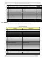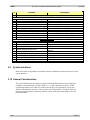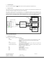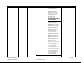
1
10 to 40W 1:1 Uplink
Downlink Redundant
System
Operation and Maintenance Manual
This page has been intentionally left blank.
mitec telecom inc.
Designers and manufacturers of telecom and wireless products
9000 Trans Canada,
Pointe-Claire, Quebec, Canada
H9R 5Z8
OPERATION AND MAINTENANCE MANUAL
Preliminary
Released
REVISION RECORD
Revision
1
ECN #
Description
Date
Preliminary Release.
CM Approval
Approved
25 Nov 05
TITLE:
10 to 40W 1:1 Uplink Downlink
Redundant System
This document contains information proprietary to mitec telecom inc., or its affiliates, or to a third party to which mitec telecom inc. may have a legal obligation to protect
such information from unauthorized disclosure, use, or duplication. Any disclosure, use, or duplication of this document or of any of the information contained herein is
expressly prohibited except as mitec telecom inc. may otherwise agree in writing.
Designer: Marina Lissianskaia
Date: 25 Nov 05
Technical Writer: C. Strunga
Date: 25 Nov 05
REV 1
DOCUMENT NO.
210590MA
PAGE 1 OF 60
This page has been intentionally left blank.
mitec
10 to 40W 1:1 Uplink Downlink Redundant System
Table of Contents
Table of Contents
1.1 General Description .................................................................................................1
1.1.1 Abbreviations ...................................................................................................1
1.1.2 System Specifications.......................................................................................2
1.2 Receiving and Inspection .........................................................................................3
1.2.1 Equipment Damage or Loss .............................................................................5
1.2.2 Return of Equipment ........................................................................................5
1.3 Preparing for Installation ........................................................................................5
1.3.1 Safety Precautions ............................................................................................6
2.1 Outdoor Unit (ODU) ................................................................................................7
2.1.1 WRK-596446-485-ES-02 Uplink Redundant Kit ............................................7
2.1.1.1
2.1.1.2
2.1.2
2.1.3
Assembly of WRK-596446-485-ES-02 HPA Redundancy Kit .......................... 7
Attach Sub-assemblies to Mounting Frame ........................................................ 7
WRK-340420RX-ES-02 Downlink LNB Redundancy Kit Assembly.............9
Securing the ODU Components to the Antenna Feed......................................9
2.2 Indoor unit (IDU) ...................................................................................................10
2.2.1 Environmental Conditions..............................................................................10
2.2.2 Safety ..............................................................................................................10
2.2.2.1
2.2.3
Electrical ........................................................................................................... 10
Connecting the IDU to the ODU ....................................................................11
3.1 General ....................................................................................................................13
3.2 Outdoor Module .....................................................................................................13
3.2.1 40W L-Band to C-Band BUC ........................................................................13
3.2.2 Low Noise Block (LNB) ................................................................................13
3.2.2.1
3.2.2.2
3.2.3
Power Requirements ......................................................................................... 13
Interface Definition........................................................................................... 13
Junction Box...................................................................................................14
3.3 Indoor Module ........................................................................................................14
3.3.1 Front Panel......................................................................................................14
3.3.2 LCD Menu Controls .......................................................................................15
3.3.2.1
3.3.2.2
3.3.2.3
3.3.2.4
Main Menu........................................................................................................ 15
Navigation......................................................................................................... 15
Menu Mode....................................................................................................... 15
View Mode ....................................................................................................... 15
3.4 Rear Panel ...............................................................................................................16
Rev 1
P-1
mitec
10 to 40W 1:1 Uplink Downlink Redundant System
Table of Contents
3.5 Functional Overview ..............................................................................................17
3.5.1 IF Input/Output Switching Module ................................................................18
3.5.2 Power Supply Modules...................................................................................18
3.5.3 Bias Tee Module.............................................................................................19
3.5.4 Master Controller............................................................................................20
3.6 System Control Mechanism...................................................................................22
3.6.1 Modes of Operation........................................................................................22
3.6.1.1
3.6.1.2
3.6.2
Switching Criteria...........................................................................................23
3.6.2.1
3.6.3
3.6.4
Auto Control Mode ........................................................................................... 22
Manual Control Mode....................................................................................... 22
Waveguide Switch Manual Override................................................................ 23
System Alarm Relay Logic.............................................................................23
Standby Failure and Alarms ...........................................................................24
3.6.4.1
Alarm LEDs ...................................................................................................... 24
3.7 Serial Protocol.........................................................................................................25
3.8 Controls and Indicators .........................................................................................25
3.8.1 Controls ..........................................................................................................25
3.8.2 Indicators ........................................................................................................26
3.9 System Interfaces....................................................................................................27
3.10
General Considerations ..................................................................................27
4.1 Preventive Maintenance.........................................................................................29
4.1.1 WRK-596446-485-ES-02...............................................................................29
4.1.2 WRK-340420RX-ES-02.................................................................................29
4.1.3 WRK-340145-485-IS-01 ................................................................................29
APPENDIX A ...................................................................................... 1
Drawings & Schematic Diagrams .................................................................................1
APPENDIX B ...................................................................................... 1
System Interface Details.................................................................................................1
APPENDIX C ...................................................................................... 1
Serial Protocol Documentation .....................................................................................1
APPENDIX D ...................................................................................... 1
Bench Test Record..........................................................................................................1
APPENDIX E ...................................................................................... 1
Rev 1
P-2
mitec
10 to 40W 1:1 Uplink Downlink Redundant System
Table of Contents
Spare Parts ......................................................................................................................1
List of Tables
Table 1 – Abbreviations and Definitions.............................................................................1
Table 2 – System RF Specifications ....................................................................................2
Table 3 – System Electrical Specifications..........................................................................3
Table 4 – Shipping Container Contents...............................................................................4
Table 5 – WRK-596446-485-ES-02 Components for Assembly ........................................7
Table 6 – LNB Power Requirements .................................................................................13
Table 7 – LNB Power Requirements .................................................................................13
Table 8 – WRK-340145-485-IS-01 Front Panel Features .................................................14
Table 9 – WRK-340145-485-IS-01 Rear Panel Features ..................................................16
Table 10 - IF Switching Module Specifications ...............................................................18
Table 11: Power Supply Technical Specifications ............................................................18
Table 12 - Bias-Tee Technical Specifications ...................................................................19
Table 13: Master Controller Technical Specifications ......................................................20
Table 14: System Controls.................................................................................................25
Table 15: System Indicators ..............................................................................................26
Table 16 - Main Component Placement ............................................................................31
Table 17 - List of System Modules vs. Module ID Reference ............................................3
Table 18 - Interface Summary .............................................................................................3
Table 19: In Door Unit RS-485_ M&C Interface................................................................5
Table 20: In Door Unit Discreet_ M&C Interface...............................................................5
Table 21: In Door Unit RS-232_ M&C Interface................................................................5
Table 22: In Door Unit Switching_System_Interface .........................................................6
Table 23: In Door Unit IF Interfaces ...................................................................................7
Table 24: In Door Unit AC Power Interface........................................................................7
Table 25: Junction Box M&C / SW CTRL Interface ..........................................................8
Table 26: Junction Box Switch_CTRL_1 Interface ............................................................9
Table 27: Junction Box Switch_CTRL_3 Interface ............................................................9
Table 28: Junction Box M&C_A Interface..........................................................................9
Table 29: Junction Box M&C_B/U Interface......................................................................9
Table 30: LNB Interfaces ..................................................................................................10
Table 31: BUC/Booster Interfaces.....................................................................................10
Table 32: RF Ports and Control Interface for Downlink Switch 1 ....................................11
Table 33: RF Ports and Control Interface for Uplink Switch 1 .........................................11
List of Figures
Figure 1 – System Block Diagram.......................................................................................1
Figure 2 – Shipping Container Layout Diagram .................................................................4
Figure 3 – C-Band Redundancy Control Switch/Term/Flex WG Sub-Assy .......................8
Figure 4 – WRK-340145-485-IS-01 Front Panel ..............................................................14
Figure 5 – WRK-340145-485-IS-01 Rear Panel ...............................................................16
Figure 6 – IDU Detailed Block Diagram...........................................................................17
Figure 7 - Internal Top-view..............................................................................................30
Figure 8 – Detailed System Block Drawing ........................................................................3
Rev 1
P-3
mitec
10 to 40W 1:1 Uplink Downlink Redundant System
Preface
Preface
Scope
This document covers the installation of the 10 to 40W 1:1 Uplink Downlink Redundant System.
It contains information intended for engineers, technicians and operators working with the
redundant system.
To make inquiries, or to report errors of fact or omission in this document, please contact mitec
telecom inc. at (514) 694-9000.
IMPORTANT
Important information concerning the operation and care of this product, as well as safety of
authorized operators is highlighted throughout this document by one of the following labels:
NOTE
Indicates a reminder, a special consideration, or additional
information that is important to know.
CAUTION!
Identifies situations that have the potential to cause equipment
damage.
WARNING!!
Identifies hazardous situations that have the potential to cause
equipment damage as well as serious personal injury.
Rev 1
P-1
mitec
10 to 40W 1:1 Uplink Downlink Redundant System
Introduction
1 Introduction
1.1
General Description
The 1:1 uplink/downlink redundant system is comprised of an outdoor (ODU) Uplink Redundant
Assembly, an outdoor Downlink Redundant Assembly and as indoor (IDU) system controller. It
provides redundant control for both the uplink and downlink applications.
The outdoor component of the system consists of:
•
A 1:1 Uplink Redundant Kit, WRK-596446-485-ES-02, containing two 40-Watt LBand to C-Band Hub Mount Block-up converters (BUCs), mitec model WTX596446-70-ES-35 with a WR137 waveguide switch assembly, assembled on a
mounting plate;
•
One junction box assembled on the WRK-596446-485-ES-02 mounting plate, that
combines the two booster Monitoring and Control interfaces and links the outdoor
unit (ODU) to the indoor controller (IDU).
•
A section of WR137 flexible waveguide for uplink connection to the antenna;
•
A 1:1 Downlink Redundant Kit, WRK-340420RX-ES-02, containing two C-band to
L-Band Hub Mount Block-Down converters (LNBs) with a WR229 waveguide
switch assembly.
The indoor component of the system is a 1:1 Up/Downlink Controller, 2RU rack-mount mitec
model WRK-340145-485-IS-01. It is connected to the ODU through its junction box and cables
and provides all monitoring and control functions.
For the component interconnections and module definitions, refer to the System Block Diagram,
Figure 1.
Rev 1
Page 1
mitec
10 to 40W 1:1 Uplink Downlink Redundant System
Introduction
VAC1
VAC2
Down Link
A3 (LNB-A)
A4 (LNB-S/B)
A7 (Downlink SW1)
WR229 W/Gs
50Ohm Termination
J0 - RS-485 M&C
J1 - DISCRETE M&C
J2 - RS-232 M&C
Rx - from Antenna
(WR229)
INTERCONNECT
J3 - SYSTEM INTERFACE
IDU CONTROLLER
A1 (IDU)
A2 (JUNCTION BOX)
210242-100
210243-100
210244
210245
210561-100
Up Link
A5 (BUC-A)
A6 (BUC-S/B)
A10 (Uplink SW1)
WR137 W/Gs
50Ohm Termination
Up_Link A IF 1 IN
Down_Link A IF 1 OUT
Tx - into Antenna
(WR137)
BUC-A VAC (210241-100)
BUC-BU VAC (210241-100)
Figure 1 – System Block Diagram
1.1.1
Abbreviations
Table 1 lists the abbreviations that may appear within this manual.
Table 1 – Abbreviations and Definitions
Abbreviation
A
AC
B/U
BUC
ºC
dB
dBm
DC
GHz
HPA
IDU
IF
IM-3
LNB
LO
M&C
MHz
N/A
ODU
P1dB
RF
SCL
SSPA
Rev 1
Description
Ampere
Alternating Current
Back Up
Block Up Converter
Degrees Celsius
Decibel
Decibel referenced to mW
Direct Current
Gigahertz (106 cycles per second)
High Power Amplifier
In Door Unit
Intermediate Frequency
Third Order Intermodulation
Low Noise Block
Local Oscillator
Monitor and Control
Megahertz (103 cycles per second)
Not Applicable
Out Door Unit
Power at one dB of gain compression
Radio Frequency
Single Carrier Level
Solid State Power Amplifier
Page 1
mitec
10 to 40W 1:1 Uplink Downlink Redundant System
Abbreviation
UUT
V
VFD
W
W/G
1.1.2
Introduction
Description
Unit Under Test
Volt
Vacuum Florescent Display
Watt
Wave Guide
System Specifications
Table 2 and Table 3 summarize the electrical specifications of the 10 to 40W 1:1 Uplink Downlink
Redundant System.
Table 2 – System RF Specifications
Parameter
Specification
Up-Link
Input IF Frequency
950 to 1525 MHz
LO Frequency
4.9 GHz
Output RF Frequency
5.9 to 6.425 GHz
Output Power @ P1dB Compression point 46 dBm (40W) min
Output Power Saturation point
47 dBm (50W) typical
Conversion Gain
65 dB, nom
Gain Flatness (small signal)
±2.5 dB, nom over full band at 250C
-60 dBc/Hz, max@ 300 Hz off the carrier;
Phase Noise
-70 dBc/Hz, max@ 1 kHz off the carrier;
-80 dBc/Hz, max @ 10 kHz off the carrier;
-90 dBc/Hz, max @ 100 kHz off the carrier;
-100 dBc/Hz, max @ 1 MHz off the carrier
Spurious
IM-3
-50 dBc max, @Pout = P1dB rated
-26 dBc max@ Pout = 43dBm SCL
(Two equal signals total, 5 MHz separate)
Harmonics
-50 dBc @ P1dB nom
Output RL (cold)
-18 dB, min, with built-in output isolator
Source VSWR
1.5 :1, max (operational)
Load VSWR
1.5 :1, max (operational)
Infinite at any angle with no damage
module with built-in output isolator
Power Consumption per BUC: RF Booster 110 / 220VAC; 250 W, max
BUC
24VDC 1A max via IF cable; supplied by
IDU
Down-Link
Input RF Frequency
3.625-4.2 GHz
LO Frequency
5.76 GHz
Output IF Frequency
950 to 1525 MHz
Noise Temperature
45 K max
Conversion Gain
65 dB nom
-63 dBc/Hz, max@ 100 Hz off the carrier;
Phase Noise
-73 dBc/Hz, max@ 1 kHz off the carrier;
-83 dBc/Hz, max @ 10 kHz off the carrier;
-90 dBc/Hz, max @ 100 kHz off the carrier;
Power Consumption per LNB
Rev 1
24VDC 0.35A max.
Page 2
mitec
10 to 40W 1:1 Uplink Downlink Redundant System
Introduction
Table 3 – System Electrical Specifications
Parameter
Specification
Up-Link
IF Input Port Impedance
50 Ohm
IF Input port
DC Block;
10MHz Block
10MHz Reference Source
0±5dBm; 10-8 stability; injected into each IF line
DC Supply
24VDC 2A max; injected into IF line
Down-Link
IF Output Port Impedance
75 Ohm
IF Output Port
DC Block;
10MHz Block
DC Supply
24VDC 0.5A max; injected into IF line
Power Supply
1.2
AC Input
Two 110/220 VAC Auto ranging; 160W max each
DC Output 1
Two 24VDC 4 A min
DC_OUT1 Efficiency
85% nom
DC Output 2
Two 12VDC 2.5 A min
DC_OUT1 Efficiency
80% nom
Receiving and Inspection
The redundant kit will arrive in a custom designed shipping container. Immediately upon receipt
of the Redundant Kit, check the Bill of Lading against the actual equipment you have received.
Inspect the shipping container exterior for visible damage incurred during shipping.
The customized wooden shipping crate is constructed to include individual interior boxes that
hold the individual components of the system. Refer to Figure 2 and Table 1 for details.
Rev 1
Page 3
mitec
10 to 40W 1:1 Uplink Downlink Redundant System
Introduction
Figure 2 – Shipping Container Layout Diagram
Table 4 – Shipping Container Contents
Interior Box
Designation
Cx4
Dx2
E
F
G
Contents
Qty 2: WTX-596446-70-ES-35 - C-Band BUC (1 per box)
Qty 1: WRK-340420RX-ES-02 - L-Band 1:1 Downlink Redundant Kit
Qty 1: C-Band WG/Switch Sub-assembly
Qty 1: 7507257-01 Base Mounting Plate
Qty 1: WRK-340146-485-IS-01 IDU Controller
Spare space
Qty 1: 210251-000AD Junction Box
Qty: 1 Hardware Kit
Qty 1: Operating Manual
Qty 1: 210536-001 Flexible Waveguide Assembly
CAUTION!
Handle the redundancy kit with extreme care. Excessive shock may
damage the redundancy kit’s delicate internal components.
Rev 1
Page 4
mitec
10 to 40W 1:1 Uplink Downlink Redundant System
Introduction
NOTE
Before unpacking the shipping container, move them near to the
site where it will be mounted. Ensure that the containers are
oriented correctly in accordance with the “This Side UP ”labels.
Carefully remove the SSPAs and accessories from the shipping
containers.
Verify that all items have been received and undamaged during shipment. Verify that all items
are complete. If there are any omissions or evidence of improper packaging, please notify Mitec
Telecom Inc. immediately.
1.2.1
Equipment Damage or Loss
Mitec Telecom Inc. is not responsible for damage or loss of equipment during transit. For
further information, contact the responsible transport carrier.
When declaring equipment as damaged during transit, preserve the original shipping cartons to
facilitate inspection reporting.
1.2.2
Return of Equipment
When returning equipment to Mitec for repair or replacement:
1. Identify, in writing, the condition of the equipment,
2. Refer to the sales order, Purchase Order and the date the equipment was received,
Notify Mitec Sales Administration Department of the equipment condition and obtain a Return
Material Authorization (RMA) number and shipping instructions. Mitec will pay for the cost of
shipping the product to the customer after the repairs are completed.
NOTE
Do not return any equipment without an RMA number. This is
important for prompt, efficient handling of the returned
equipment and of the associated complaint.
1.3
Preparing for Installation
Before attempting to install or use the 10 to 40W 1:1 Uplink Downlink Redundant System, we
recommend that you first familiarize yourself with the kit by reading through this manual.
Understanding the operation of the redundant kit will reduce the possibility of incorrect
installation, thereby causing damage or injury to yourself or others.
Rev 1
Page 5
mitec
10 to 40W 1:1 Uplink Downlink Redundant System
Introduction
The redundant kit must be installed in accordance with the
conditions and recommendations contained in the following
sections.
When you are ready to begin your installation, use the information in Chapter 2 (Installation) as a
guide for making all the required electrical connections.
1.3.1
Safety Precautions
Carelessness or mishandling of the redundant kit may damage the unit causing serious injury to
yourself or others. Please adhere to the following:
Rev 1
Page 6
This page has been intentionally left blank.
mitec
10 to 40W 1:1 Uplink Downlink Redundant System
Installation
2 Installation
This section describes the installation and theory of operation of the redundant system.
2.1
Outdoor Unit (ODU)
2.1.1
WRK-596446-485-ES-02 Uplink Redundant Kit
NOTE
An O-ring shall be used to seal each waveguide connection.
2.1.1.1
Assembly of WRK-596446-485-ES-02 HPA Redundancy Kit
Use the information in this section as a guide to assemble and install the redundant kit. The
system is designed to function outdoors with the specified humidity up to 100% during operation.
However, installation should be carried out in dry conditions, free of salt spray or excessive
humidity. This will eliminate the possibility of moisture and other foreign substances from
entering the output waveguide flange.
CAUTION!
Only authorized technical personnel should perform the
Installation and proper electrical hookups of the redundant
system.
Table 5 lists the parts of the WRK-596446-485-ES-02 that are shipped separately. Mounting
brackets, hardware and gaskets are included to complete the assembly. Refer to the assembly
drawing in Appendix A for further details.
Table 5 – WRK-596446-485-ES-02 Components for Assembly
Description
Mounting Frame
40 W C-Band HPA with BUC
Junction Box
Redundancy Switch/HP Term/Flex WG Assy
Switch Assy Mounting Bracket
2.1.1.2
Rev 1
Part Number
7507257-01
WTX-596446-70-ES-35
210251-001
210497
Qty
1
2
1
1
1
Attach Sub-assemblies to Mounting Frame
Page 7
mitec
10 to 40W 1:1 Uplink Downlink Redundant System
Installation
With reference to the assembly drawing, WRK-596446-485-ES-02AD, in Appendix A, complete
the following steps to assemble the WRK-596446-485-ES-02.
1. Attach the Redundancy Control Switch/Term/Flex WG Assembly (See Figure 3) with the
mounting bracket PN 210497, using the appropriate hardware as specified on the
assembly drawing.
Figure 3 – C-Band Redundancy Control Switch/Term/Flex WG Sub-Assy
2. Secure this assembly to the mounting frame PN 7507257-01. Use hardware as specified
as per the assembly drawing.
3. Assemble the cables to the junction box, as shown in drawing 21051-001AD in Appendix
A. Fasten the junction box, PN 210251-001 to the mounting frame, using the specified
hardware as per the assembly drawing.
4. Attach both HPA Systems to the mounting frame, as per the assembly drawing in
Appendix A, using the specified hardware as per the assembly drawing. Do not torque
the fasteners all the way until the waveguide interconnections are completed.
5. Complete the connections between the waveguide flanges (2) and the booster outputs.
Use O-Rings and hardware as specified. Ensure the waveguide is not under tension, and
then tighten the fastening hardware to fix the position of the SSPAs on the frame.
6. Install the cable assemblies between the junction box and the WRK-596446-485-ES-02
assemblies. Refer to the detailed block diagram and the cable drawings in Appendix A.
The WRK-596446-485-ES-02 is now ready for assembly the antenna feed support.
Rev 1
Page 8
mitec
10 to 40W 1:1 Uplink Downlink Redundant System
Installation
NOTE
Both SSPAs contain two high flow-rate fans (300 CFM) for
cooling the RF Amplifier Module. These fans function
continuously during the booster operation. To provide a
sufficient airflow, the booster should be mounted with a
minimum clearance of 3 inches on the bottom and all four sides.
Adequate cooling for the boosters will provide years of top
performance.
2.1.2
WRK-340420RX-ES-02 Downlink LNB Redundancy Kit Assembly
With reference to the WRK-340420RX-ES-02AD assembly drawing in Appendix A, assemble
the waveguide bends, LNBs waveguide switch and waveguide termination, using the included
specified hardware and gaskets.
2.1.3
Securing the ODU Components to the Antenna Feed
Complete the following steps to complete the installation of the ODU.
1. Install the components of the WRK-596446-485-ES-02 Redundant System onto the
antenna feed support through the mounting holes on the frame, using the specified
hardware. Refer to the system assembly drawing, 210590AD in Appendix A,
2. Carefully install the connecting flexible waveguide assembly between the WRK-596446485-ES-02 output waveguide flange, using the specified gaskets and hardware, as
illustrated in the system assembly drawing 210590AD in Appendix A.
3. Install the WRK-340420RX-ES-02AD Redundant System onto the antenna feed by
completing the waveguide flange connection, using the specified gaskets and hardware,
as illustrated in the system assembly drawing, 210590AD in Appendix A.
4. Install the interconnecting cables from the WRK-340420RX-ES-02 waveguide switch to
the junction box. Refer to the detailed block diagram and the cable drawings in Appendix
A.
5. Ensure all connections are secure and torqued.
WARNING!!
It is preferable that all coaxial cables are installed before the
system is powered up. Once powered up, there is 24 VDC on all
coaxial connections, which could be easily shorted when a cable
is connected. Should such a short occur, the system will react
appropriately and the shorted line will be turned off until the
short is removed. No damage will occur.
Rev 1
Page 9
mitec
2.2
10 to 40W 1:1 Uplink Downlink Redundant System
Installation
Indoor unit (IDU)
The IDU controller is a standard 2 RU chassis, which can be mounted in an EIA-standard 19-inch
equipment rack. If the controller is to be mounted in a rack, be sure to allow adequate clearance
at the rear of the unit for attaching the cables.
NOTE
Recommended clearance above and below the unit is 3.5 inches.
Allow a minimum clearance of 1.75 inches.
CAUTION!
Do not mount the unit using only the front panel mountings -the
unit is too heavy. Failure to properly support the unit from front
to back will deform the front panel and cause internal mechanical
damage.
2.2.1
Environmental Conditions
Operate and store the IDU in a dry, well-ventilated area with a minimum of dust and vibration.
Operating temperature range: 00C to +500 C.
Operating relative humidity range: 5% to 90%
Install the unit in an area protected form excessive dust and humidity. Failure to do so will result
in malfunction or damage, and will reduce the service life of the unit.
CAUTION!!
Keep liquids away from the unit. Liquids penetrating to the
interior of the unit will cause malfunction or equipment damage.
2.2.2
2.2.2.1
Safety
Electrical
Carelessness, or mishandling of the controller may damage the unit causing injury. Please adhere
to the following:
Rev 1
Page 10
mitec
10 to 40W 1:1 Uplink Downlink Redundant System
Installation
WARNING!!
The unit is equipped with AC power cords and plugs. Do not
tamper with, or attempt to reconfigure the cords or plugs
supplied with the unit, as this can result in personal injury and
void the warranty.
Always disconnect the power cords before attempting to:
2.2.3
•
Unplug the connectors
•
Replace parts
•
Clean the unit
Connecting the IDU to the ODU
Once the IDU has been installed, attach the cables from the components of the ODU to the
appropriate rear panel connectors on the controller. Refer to the detailed block diagram in
Appendix A for cable details.
The system should now be fully installed and connected.
Rev 1
Page 11
This page has been intentionally left blank.
mitec
10 to 40W 1:1 Uplink Downlink Redundant System
Operation
3 Operation
This section describes the operation of the 1:1 Uplink/downlink Redundant System.
3.1
General
The Uplink Outdoor unit consists of two 40W L-Band to C-Band BUCs, WTX-596446-70-ES-35
and the output WR137 Redundancy Switch.
The Downlink Outdoor unit consists of two C-Band to L-Band LNBs, manufacturer part ID
NJS8477HN and the Input WR229 Redundancy Switch.
3.2
Outdoor Module
3.2.1
40W L-Band to C-Band BUC
This is a standard Mitec product, WTX-596446-70-ES-35. It contains a high gain low power
Block-Up Converter (BUC) and a 40W High Power Amplifier (HPA). For additional details,
please refer to its Operation and Maintenance Manual.
3.2.2
Low Noise Block (LNB)
This is a standard purchased item NJS8477SF, manufactured by NJRC.
3.2.2.1
Power Requirements
Table 6 – LNB Power Requirements
Parameter
Specification
Current per LNB
0.35A max. at 24 VDC
DC Supply voltage
3.2.2.2
15 to 24 VDC
Interface Definition
Table 7 – LNB Power Requirements
Connector
J1 RF In
Connector Type
Signal parameter
CPR229
RF In
J2 IF Out
N-type Female
For further details please refer to the LNB user manual.
Rev 1
24 VDC 0.34A max.
Page 13
mitec
3.2.3
10 to 40W 1:1 Uplink Downlink Redundant System
Operation
Junction Box
The junction box for the ODU is located on the mounting plate with the BUCs. If provides the
M&C interface between the ODU and the IDU controller. Refer to Appendix B for the connector
interface pinout information.
3.3
Indoor Module
3.3.1
Front Panel
The WRK-340145-485-IS-01 controller front panel is divided into 5 sections, which include the
following features;
♦ System Status VFD Display – displays the uplink and downlink and alarm statuses, with
push-button and menu controls.
♦ Mode indication and push-button controls;
♦ System Element Status LED display;
♦ Redundancy Status LED controls and alarm display;
♦ Sub-system toggle controls.
The front panel appears in Figure 4. Its controls and indicators are listed in Table 5.
1
2
3
4
5
6
7
Figure 4 – WRK-340145-485-IS-01 Front Panel
Table 8 – WRK-340145-485-IS-01 Front Panel Features
Item
Rev 1
Description
1
VFD Display screen
2
Mode selection push buttons and LED display
3
MAIN MENU push button control
4
Direction arrows and select push buttons
5
System Element Status LED display
6
Redundancy Status LED display
7
Toggle Push button controls
Page 14
mitec
3.3.2
10 to 40W 1:1 Uplink Downlink Redundant System
Operation
LCD Menu Controls
On start up, the LCD display will first flash "Mitec", and then display the schematic of the uplink
system, with the blinking cursor at the bottom of the screen on the DOWNLINK label. Pushing
Select will display the downlink schematic.
Pushing the MAIN MENU button will display the top-level menu. From here, the user can toggle
through the various lower-level screens to view the settings and statuses of the system and the
elements that make up each chain. At any time, the user can push the MAIN MENU push button
to return to the top-level menu.
NOTE
Chain B is an option for the 1:2 system configuration.
3.3.2.1
Main Menu
Uplink and Downlink - Allows user to select a specific chain. Once the chain has been selected,
pushing select again will display the chain's status. At this level, the user
can also choose to Mute a chain
View - Switches to view menu with schematic display.
3.3.2.2
Navigation
The UP/DOWN arrow buttons allow the user to browse through the menu.
•
Right push button will display the lower-level menu selection options.
•
LEFT push button will return the user to the previous menu.
There are two ways of navigating through the various screens.
3.3.2.3
Menu Mode
Pushing the SELECT button will display any lower level menu associated with the chosen menu
option. By choosing an option and then pushing the select button the user will go further down in
the menu ti the status of a single system element.
3.3.2.4
View Mode
In view mode, the appropriate system (uplink/downlink) schematic will appear, displaying:
•
Switch positions indicated by icons
•
Elements of the active chain, indicated by a dot inside their icons.
•
BUC/Boosters/LNB/Switch alarms indicated by the appropriate icon blinking.
In view mode, pushing the Down arrow will move the cursor to an element in the chain. Pushing
Select in this position will display the status of the chosen element.
Rev 1
Page 15
mitec
10 to 40W 1:1 Uplink Downlink Redundant System
Operation
Use the direction push buttons to move the cursor to another element.
3.4
Rear Panel
The rear panel houses the ac input sections and all the connectors for interfacing with other
system equipment. The rear panel appears in Figure 5. Its various features are listed in Table 9.
1
6
7
12
13
8
9
10
11
2
3
4
5
Figure 5 – WRK-340145-485-IS-01 Rear Panel
Table 9 – WRK-340145-485-IS-01 Rear Panel Features
Item
Rev 1
Description
1
Power Supply Modules
2
9-pin RS-485 Interface (J0)
3
9-pin Discrete M&C Interface (J1)
4
9-pin RS-232 M&C Interface (J2)
5
37-pin System Interface (J3)
6
N-Type Female Uplink A IF IN
7
F-Type Female Downlink A IF OUT
8
N-Type Female Uplink A IF OUT
9
F-type Female Downlink A IF IN
10
N-Type Female Uplink S/B IF OUT
11
F-type Female Downlink S/B IF IN
12
N-Type Female Uplink B IF IN
13
F-type Female Downlink B IF OUT
Page 16
mitec
3.5
10 to 40W 1:1 Uplink Downlink Redundant System
Operation
Functional Overview
The major components of the WRK-340145-485-IS-01 are:
♦
♦
♦
♦
Power Supplies;
Bias Tee Modules;
Motherboard;
Switching Modules
The IDU controller detailed block diagram, Figure 6, details its main components.
Figure 6 – IDU Detailed Block Diagram
IDU Controller
AC1 In
Power Supply 1
24VDC
to IF Chain A
24VDC to:
IF Chain C
RS-485_BoostA
Control
System
AC2 In
Power Supply 2
M&C
from ODU
24VDC
to IF Chain B
Sw.Contr.
RS-485
Boost.B
ODU M&C
RS-232
Controller
RS-232 User
IF In1
IF In1
IF In12
IF In12
IF Up_A;
10MHz;
24VDC
IF Up_A;
10MHz;
24VDC
BT_UP_A Module
IF Up_B;
10MHz;
24VDC
BT_UP_B Module
IF Up_C;
10MHz;
24VDC
IF Up_C;
10MHz;
24VDC
BT_UP_C Module
IF Dn_A;
10MHz;
24VDC
IF Dn_A;
10MHz;
24VDC
BT_Down_A Module
IF Dn_B;
10MHz;
24VDC
IF Dn_B;
10MHz;
24VDC
BT_Down_B Module
IF Dn_C;
10MHz;
24VDC
BT_Down_C Module
IF In Sw. Module
IF Up_B;
10MHz;
24VDC
Rear
Panel
Front
Panel
Controller
Front
Panel
CAN
IF Dn_C;
10MHz;
24VDC
IF Out1
IF Out2
IF Out1
IF Out Sw. Module
IF Out1
Refer to Figure 7 for the location of the modules within the WRK-340145-485-IS-01 cabinet.
Rev 1
Page 17
mitec
3.5.1
10 to 40W 1:1 Uplink Downlink Redundant System
Operation
IF Input/Output Switching Module
The IF Input/Output Switching module is a plug-in PCB card providing configurable IF path
switching for a 1:1 redundancy configuration.
The IF IN switching module provides switching from one IF In port (from the modem) to one
output of two Bias Tee modules (IF_OUT-A or IF_OUT-B).
The IF OUT module provides switching from one IF OUT Port (going to the model) to one OUT
of two Bias Tee Modules (IF_OUT_A or IF_OUT_B).
Table 10 - IF Switching Module Specifications
Parameter
Specification
Frequency
950MHz to 1525MHz
Impedance
50 Ohm
Return Loss at IF In/Out_1 and IF In/Out_2
-14dB max
Return Loss at IF In/Out_A,B,C
-14dB max
Insertion Loss
-3dB nom any IF path
Switch Control
CAN Interface
DC Supply Voltage
TBD
IF In/Out port DC characteristics
DC Block
IF In/Out port 10MHz Isolation
-40dBc max
2 x 2 N-type female
3 x 2 SMA female
TBD
TBD
Connectors: IF In / Out_1/2
IF_In/Out_A/B/S-B/C
DC Supply
CAN Interface
3.5.2
Power Supply Modules
The Power Supply Modules convert two redundant 90 to 260VAC 50-60Hz input AC voltages
into 24VDC voltage supplying power to all IDU modules as well as to the BUCs and the LNBs
within the ODUs .
Power is applied to the WRK-340145-485-IS-01 using the ON/OFF switches in the rear panel
power input sections. If a failure occurs in one power supply, the second power supply module is
capable of supplying ample power to continue operation. Each ac input has a 2A fuse in the line.
To replace a fuse, remove the plastic cap in the rear panel AC module, replace the fuse and
reinsert the plastic cap.
Table 11: Power Supply Technical Specifications
Parameter
Specification
Input
Rev 1
Input Voltage
90 to 260VAC 50-60 Hz AC
Input Power
2 x 180W min
External Fuses
(?)
Page 18
mitec
10 to 40W 1:1 Uplink Downlink Redundant System
Parameter
Operation
Specification
Output
DC Output Voltage
24 VDC
DC Current
3 x TBD A
Auxiliary DC Voltage
TBD
TBD
Short Circuit Protection
Connectors
TBD
3.5.3
Bias Tee Module
The Bias Tee Module with the IF path for Up/Down-Link provides the following functions:
•
Generates high stability 10MHz reference signal;
•
Injects 10 MHz reference signal into IF line;
•
Injects 24 VDC into IF line;
•
Monitors 10 MHz reference signal level, 24 VDC level, BUC/LNB current consumption
•
Provides IF line Mute Control
•
Provides all IF line telemetry via CAN Interface.
Table 12 - Bias-Tee Technical Specifications
Parameter
Specification
IF Parameters
Input/Output IF Frequency
950 to 1525 MHz
Impedance
50 Ohm
Input/output Return Loss
-12 dB max
Output/Input Return Loss A/B/S-B/C (cold)
-12 dB max
Insertion Loss
5 dB nom
Reference Signal Frequency
10 MHz
Frequency Stability vs. Temperature
1x10e-8
Aging
5x10e-8/year
10MHz Source Warm Up Time within 10e7
3 min max
10 MHz Output A/B/S-B
3 dBm min
10 MHz isolation to input
-50 dBc nom
10MHz level at IF Output/Input port
2dBm min
-115 dBc/Hz, max@ 10 Hz off the carrier;
-140 dBc/Hz, max@ 100 Hz off the
carrier;
-150 dBc/Hz, max @ 1 kHz off the carrier;
10MHz Source Phase Noise
Rev 1
Page 19
mitec
10 to 40W 1:1 Uplink Downlink Redundant System
Parameter
Operation
Specification
M&C Functions (via CAN)
Summary Alarm Status
Broadcast in case of alarm
10MHz Alarm (when polled)
If 10MHz level is below –10 dBm (?)
24VDC Alarm (when polled)
If DC supply voltage is below 15VDC
BUC/LNB Low Current Alarm (when
polled)
If BUC/LNB current consumption is
below Threshold
BUC/LNB High Current Alarm (when
polled)
If BUC/LNB current consumption is
below Threshold
Mute Status (when polled)
Mute Control
High Current Threshold Setting
Remembers setting at Power up
Low Current Threshold Setting
Remembers setting at Power up
Power Supply
DC Supply Voltage
24VDC 2A min
Auxiliary Supply Voltage
(?) 5VDC 1A min
Short circuit protection
Overcurrent Shut Down (recoverable) at
current consumption >4A (?)
Connectors
3.5.4
IF Input/Output Connector
SMA female
IF Output/Input Connector
N-type female (rear panel)
10MHz Auxiliary
SMA female
CAN
TBD
DC Supply
TBD
Master Controller
The Master Controller communicates with the ODUs via RS-485 Serial Interface. It
communicates with all IDU modules on the CAN BUS. It provides all System telemetry to the
user via RS-232 or RS-485 User Interface. Master Controller makes decisions on System
Redundancy Functions (?).
Table 13: Master Controller Technical Specifications
Parameter
Specification
Interfaces
Booster (ODU) Serial Interfaces
3 x RS-485 half-full duplex compatible
Internal IDU Interface
CAN
Serial User Interface
RS-485 or RS-232 (both available)
Discrete User Interface
Contact Closure (?)
Discrete ODU interface
ODU Switches Control/Telemetry
ODU Boosters Discrete Telemetry (contact
closure)
Rev 1
Page 20
mitec
10 to 40W 1:1 Uplink Downlink Redundant System
Parameter
Operation
Specification
Control and Indicators via Booster Serial Interface
Booster A/B/S-B/C Status
Active/Muted/Alarm
Booster A/B/S-B/C Output Power
20dB Dynamic Range
Booster A/B/S-B/C Case Temperature
Deg.C
Booster A/B/S-B/C Overtemperature
Alarm
Case temperature >85deg.C +3/-5 deg.C
Booster A/B/S-B/C Com Status
Operational/Fault
Booster A/B/S-B/C Mute Control
Control and Indicators via Booster Discrete Interface
Booster Summary Alarm
Form C Relay (?)
Booster Mute Control
Contact Closure (?)
ODU Switch Control Interface
TBD
Control and Indicators via User Serial Interface
See Tables in Paragraphs 2.2.1 and
2.2.2
Control and Indicators via User Discrete Interface
System Status
Operational / Fault – Contact Closure
BUC-Booster A / B / C Status
Operational / Fault – Contact Closure (?)
Redundancy Controls and Indicators
Up/Down Link Chain A/B/S-B/C
status
W/G Switches Up/Down - 1 / 2
Position
Coax Switches Up/Down - 1 / 2
Position
Active/Stand by/Fault via:
User Serial Interface;
CAN Interface (to the Front Panel Controller)
via:
User Serial Interface;
CAN Interface (to the Front Panel Controller)
via:
User Serial Interface;
CAN Interface (to the Front Panel Controller)
via:
Switch Up/Down Link Control
Switch Control interface and CAN (to the Input
Switching Module)
User Serial Interface;
CAN Interface (from the Front Panel Controller)
Power Supply
Supply Voltage
Rev 1
5VDC 0.3A steady state; ?A peak Redundant
Page 21
mitec
3.6
10 to 40W 1:1 Uplink Downlink Redundant System
Operation
System Control Mechanism
3.6.1
Modes of Operation
The 1:1 Redundancy System Remote Controller WTX-340145-485-IS-01 can operate in:
•
Auto Redundancy Control Mode
•
Manual Redundancy Control Mode.
The current operating mode of the controller is reported on the front panel LED display.
NOTE
Auto Control Mode is a default mode of operation. The system is
in Auto Control Mode when is powered up, even if it was in
Manual Control Mode when was powered down. The reset
Command also sets the system to Auto Control Mode.
3.6.1.1
Auto Control Mode
In Auto Control Mode, it provides all redundancy functions automatically. It constantly monitors
and analyzes all subsystem statuses, decides on switching and executes switching from active to
stand by unit when necessary. It allows the user to toggle from the active to the standby unit as
long as the standby unit is not faulty.
All controls permitted in Auto Mode are available remotely via the RS-232/RS-485 User
Interface or via the Remote Control panel. There is a Local/Remote Control Button on the Front
Panel to switch from control via serial interface to local control using Front Panel. (Refer to
Figure 4.)
3.6.1.2
Manual Control Mode
Manual Control Mode can be chosen for maintenance purposes, or in case if redundancy
controller malfunctions. The system can be remotely switched to manual control mode via user
serial interface or locally using front panel push button.
NOTE
In Manual Control Mode, the controller also provides all system
monitoring, as in Auto Mode. However, in Manual Control Mode
the controller only executes user commands and does not make
any decisions on switching from a faulty unit.
Rev 1
Page 22
mitec
10 to 40W 1:1 Uplink Downlink Redundant System
Operation
3.6.2 Switching Criteria
The following events will trigger the up-link to automatically switch from active to stand by unit:
•
The 10MHz signal level on the active chain is below threshold (Out of Lock Alarm).
The affected chain BUC RED LED (A or S/B) will be illuminated;
•
The active BUC current consumption is below low threshold or above high threshold
(BUC Current Alarm). The affected chain BUC RED LED (A or S/B) will be
illuminated;
•
The active booster reports a Summary Alarm (Booster Alarm). The affected chain
BUC RED LED (A or S/B) will be illuminated;
•
The active Booster does not respond via the RS-485 interface (Booster Com Status
Alarm). The affected chain BUC RED LED (A or S/B) will be illuminated.
The following events will trigger the downlink to automatically switch from active to stand by
unit:
•
3.6.2.1
The active LNB current consumption is below high threshold or above high threshold
(LNB Current Alarm) The affected chain LNB RED LED (A or S/B) will be
illuminated;
Waveguide Switch Manual Override
If the user changes the switch positions by manually turning the switch override directly on the
waveguide switch, the system will follow by switching the corresponding IF switch to the same
position.
3.6.3 System Alarm Relay Logic
Following is a summary of the system alarm relay logic.
Uplink Relay will declare an alarm if:
• The uplink waveguide switch is in alarm
•
Any one of the BUCs is in alarm (not 10MHz alarm)
•
Any Booster is in alarm
Downlink Relay will declare an alarm if:
• The downlink waveguide switch is in alarm
•
Any one of the LNBs is in alarm
System Relay will declare an alarm if:
•
Any power supply fails
•
An IF switch fails
•
Bias-Tee (10MHz) Alarm
•
IF switch board communication alarm
The "SYSTEM STATUS" LED on the front panel will show an alarm if no uplink chain is
operational or no downlink chain is operational. Conditions that can cause the system failure
include;
Rev 1
Page 23
mitec
10 to 40W 1:1 Uplink Downlink Redundant System
Operation
•
Both uplink chains are in alarm
•
Both downlink chains are in alarm
•
A waveguide switch is out of position
•
One uplink chain AND the other power supply are in alarm, or one downlink chain
AND the other power supply are in alarm.
3.6.4 Standby Failure and Alarms
In AUTO mode, a standby unit exhibits any of the alarms listed above, the redundancy controller
will not switch. It will broadcast System Failure via the user serial interface and the front panel
LEDs, and will turn ON the audible alarm on the remote control panel. Pushing any of the display
control push buttons will switch the audible alarm OFF. The audible alarm can be switched OFF
permanently in the System Settings Display Menu. It will be reset back on again after the system
is powered down and then powered up.
The System Failure will be also be reported when any of the following conditions occur:
•
•
•
•
•
•
3.6.4.1
Up-Link W/G Switch Failure (Uplink Switch1 Alarm RED LED will be illuminated);
Up-Link Coax switch Failure (Uplink Switch1 Alarm RED LED will be illuminated);
Downlink W/G Switch Failure (Downlink Switch1 Alarm RED LED will be
illuminated);
Downlink Coax Switch Failure (Downlink Switch1 Alarm RED LED will be
illuminated);
Redundancy Controller failure;
Both Power Supplies fail.
Alarm LEDs
Following is a more detailed description of the conditions that will illuminate an alarm LED.
Switch Alarm (Uplink or Downlink)
When either an IF or RF switch is stuck between positions, cannot move to the other position or
when the switches are out of synchronization, the affected switch alarm RED LED will
illuminate. If the switch if stuck between positions, the redundancy switching controller will
attempt to try to reposition the switch 5 times, in 0.5 second intervals. If it is still stuck, the
controller will declare a system alarm and repeat these retries every 30 seconds. When the
waveguide switch is stuck between positions, the controller will try to drive it by default to side
A, then if side A is in alarm, normal logic takes place. If the switch is out of synchronization, the
controller will attempt to return it to normal, as follows:
1. Treating the waveguide switch as the master, the controller will first try to synchronize
the IF switch with the waveguide switch.
2. If this is unsuccessful, the controller will try to move the IF switch to the same position as
the waveguide switch.
Rev 1
Page 24
mitec
10 to 40W 1:1 Uplink Downlink Redundant System
Operation
BUC Alarm (A or S/B)
The affected BUC RED alarm LED will illuminate if the following conditions occur:
•
10 MHz Alarm;
•
BUC over current (or low current); this is latching. It will remain on even when the
over current disappears. The controller reset via RS-232 is required to remove this
alarm.
•
Short circuit on an IF line; will recover once the short circuit condition is removed.
•
Booster Summary alarm;
•
Communication Alarm.
LNB Alarm (A or S/B)
The affect LNB RED alarm LED will illuminate if the following conditions occur:
•
LNB over current (or low current); this is latching. It will remain on even when the
over current disappears. The controller reset via RS-232 is required to remove this
alarm.
•
Short circuit; will recover once the short circuit condition is removed.
Power Supply Alarm
A Power Supply RED alarm LED will illuminate if the DC voltage from that power supply drops
below 20V.
3.7
Serial Protocol
Refer to the serial protocol specification document for the 1:1 Up/Downlink Redundant system in
Appendix C.
3.8
Controls and Indicators
3.8.1
Controls
Table 14 describes the controls available for the various modes of operation.
Table 14 - System Controls
#
Control
Description
Controls via RS-232/485 User Interface
1
2
3
4
5
6
7
8
11
Rev 1
System Mute Control
Down-Link Mute Control
Up-Link Mute Control
BUC A/BU Mute Control
Toggle Down-Link
Toggle Up-Link
Manual Mode Control
Local/Remote Control
Reset
Mutes the System
Mutes Both LNBs
Mutes Both BUCs
Mutes BUC A/BU
Switches Active/Stand by LNB
Switches Active/Stand by BUC
User Controls Redundant System
Switches Front panel vs. RS-232 Control
Resets Microcontroller
Default
Setting
Unmuted
Unmuted
Unmuted
Unmuted
LNB A active
BUC A active
Manual Mode off
Remote Control
Page 25
mitec
10 to 40W 1:1 Uplink Downlink Redundant System
Initial
Settings
Internal Controls / Protections
14
15
16
17
BUC A/BU Out of Lock Shut Down
BUC A/BU Over Temperature Shut
Down
BUC A/BU Overcurrent Shut Down
LNB A/BU Overcurrent Shut Down
Operation
Internally Set
Internally set
+85 ± 2deg.C
Internally set for each BUC
Internally set for each LNB
± 1.5dB max
Manual Controls (Front Panel)
20
21
22
23
24
27
28
30
Up-Link Mute Control
Down-Link Mute Control
BUC A/BU Mute Control
Up-Link Toggle
Down-Link Toggle
LNB A/BU Mute Control
Local/Remote
Manual Mode/Auto Mode
System On/Off Control
Audible Alarm Reset
Push Button via Display Menu
Push Button via Display Menu
Push Button via Display Menu
Push Button Front Panel
Push Button Front Panel
Push Button via Display Menu
Push Button Front Panel
Push Button Front Panel
2 x On/Off VAC Switches Rear panel
Switches off an Audible Alarm
3.8.2 Indicators
Table 15 describes the interface and panel indicators available in each mode.
Table 15: System Indicators
#
Indicator
Description
Indicators via RS232/RS485 User Interface
1
2
3
4
5
6
7
8
9
10
11
12
13
14
15
16
17
18
19
20
21
22
Up-Link Status
Down -Link Status
Booster A/BU Status
10 MHz Reference A/BU status
LNB A/BU Status
BUC A/BU Status
Up-Link Switch Status
Down -Link Switch Status
Power Supply A Status
Power Supply B Status
Booster A Temperature
Booster BU Temperature
Booster A Output Power
Booster BU Output Power
Up-Link Output Power
Low Output Power Warning
Booster A/BU Over Temperature Alarm
Booster A/BU Com Status
BUC A/BU Over Current Alarm
BUC A/BU low current Alarm
LNB A/BU Over Current Alarm
LNB A/BU low current Alarm
23
24
25
System Status
Up-Link Status
Down-Link Status
Operating / Fault
Operating / Fault
Operational/Muted/Fault
Operational/Fault
Operational/Mute/Fault
Operational/Muted/Fault
A / BU / Fault
A / BU / Fault
Operational/Fault
Operational/Fault
Degree C
Degree C
20dB Dynamic range
20dB dynamic range
20dB dynamic range
20 dB below rated power
Operational/Fault
Operational/Fault
Operational/Fault
Operational/Fault
Operational/Fault
Operational/Fault
Indicators via Discrete Interface
Rev 1
Operational / Fault – Contact Closure
Operational / Fault – Contact Closure
Operational / Fault – Contact Closure
Page 26
mitec
#
10 to 40W 1:1 Uplink Downlink Redundant System
Indicator
Operation
Description
Panel Indicators
26
27
28
29
30
31
32
33
34
35
36
37
38
39
40
41
42
43
44
45
46
47
3.9
Front Panel LED:
System Status Bicolor LED
G-Operational / R-Fault
Power Supply A / B Status Bicolor LED
G-Operational / R-Fault
Up-Switch 1Status Bicolor LED
G-Operational / R-Fault
Down- Switch 1 Status Bicolor LED
G-Operational / R-Fault
Up-link Redundancy Status Bicolor LED
G - Active BUC / Y - Stand by BUC
Down-Link Redundancy Status Bicolor LED
G - Active LNB / Y - Stand by LNB
BUC A/B/S-B Status LED
R – Alarm; Operational - off
LNB A/B/S-B Status LED
R – Alarm; Operational - off
Redundancy Operation Mode LED
Auto Yellow LED / Manual Green LED
Control Mode
Local Green LED / Remote Green LED
Audible Alarm
Audible Alarm is on in case of System Fault
Front Panel Display
10 MHz 1 / 2 Status
Operational / Alarm
BUC A/B/S-B Status
Operational / Mute / Alarm
Booster A/B/S-B Summary Alarm Status
Operational / Mute / Alarm
Booster A/B/S-B Temperature
Deg.C
Low Power Warning/ Pout [dBm] / Overpower
Booster A/B/S-B Output Power
Warning
Booster A/B/S-B Com Status
Operational / Alarm
LNB A/B/S-B Status
Operational / Mute / Alarm
Up-Switch ½ (output) Position
A / BU / Fault
Up-Switch ½ (input) Position
A / BU / Fault
Down-Switch ½ (output) Position
A / BU / Fault
Down-Switch ½ (input) Position
A / BU / Fault
System Interfaces
Refer to the tables in Appendix B for detailed connector definitions and pinout lists for all of the
system interfaces.
3.10 General Considerations
The system shall meet all specifications over the full bandwidth and under all environmental
conditions, when terminated in a load VSWR of 1.5:1, unless otherwise specified. All RF
specifications shall be met within five minutes after the DC power application, except gain
stability, which shall be met after a warm-up period of twenty minutes. During the warm-up
period, the module shall not exhibit any alarm or require an RF mute input signal to reset any
alarm/fault latches.
Rev 1
Page 27
This page has been intentionally left blank.
mitec
10 to 40W 1:1 Uplink Downlink Redundant System
Maintenance
4 Maintenance
This chapter contains information on how to maintain, troubleshoot and repair the system. It is
extremely reliable, requiring very little preventive maintenance, or repair. Should there be a
malfunction, this chapter also contains technical information to help diagnose basic failures.
4.1
Preventive Maintenance
WARNING!
Before any maintenance is attempted, make sure that the power to
the system/unit in maintenance is turned OFF. Failure to observe
this precaution may result in personal injury. This includes the
removal of any RF power originating from other system
components
4.1.1
WRK-596446-485-ES-02
This Uplink redundant system includes two mitec standard WTX-596446-70-ES-35
BUC/boosters. Refer to the WTX-596446-485-ES-01 Operation and Maintenance manual for
maintenance instructions for these modules.
4.1.2
WRK-340420RX-ES-02
This Downlink redundant system includes two LNBs, which are manufactured by NJRC, item
numbers NJS8477SF. Refer to the LNB manufacturer for maintenance requirements.
4.1.3
WRK-340145-485-IS-01
The WRK-340145-485-IS-01 indoor redundant system controller requires no preventive
maintenance.
If internal modules require replacement, the following sequence of steps should be carried out.
Rev 1
Page 29
mitec
10 to 40W 1:1 Uplink Downlink Redundant System
Maintenance
WARNING!!
Make sure to disconnect the affected power cord before
attempting to replace parts. Failure to do so may result in
electrical shock.
1.
2.
3.
4.
Turn off power and disconnect power cords.
Slide the unit clear of the rack.
Remove hardware securing the enclosure top.
To replace a power supply module, disconnect all connections from the power supply,
replace with new part, and reconnect.
5. To replace a bias-tee or switching module, disconnect connectors and remove screws at
either end of the board supports. Replace board, refasten in place and reconnect.
Refer to the top-view in Figure 7 and Table 16 for main component placement. For clarity, wiring
has been omitted from this drawing.
9
1
8
7
6
5
4
2
3
Figure 7 - Internal Top-view
Rev 1
Page 30
mitec
10 to 40W 1:1 Uplink Downlink Redundant System
Maintenance
Table 16 - Main Component Placement
Item
Rev 1
Description
1
Power Supply Module 2
2
Power Supply Module 1
3
Master Controller
4
Uplink Switching Module
5
Downlink Switching Module
6
BT-UP A Module
7
BT-DOWN A Module
8
BT-UP S/B Module
9
BT-DOWN S/B Module
Page 31
This page has been intentionally left blank.
mitec
10 to 40W 1:1 Uplink Downlink Redundant System
Appendix A
Appendix A
Drawings & Schematic Diagrams
1:1 Redundancy Control System Detailed Block Diagram
WRK-596446-485-ES-02AD Assembly Drawing
210244-003 Switch Control Cable
210245-002 BUC M&C Cable
Rev 1
A-1
This page has been intentionally left blank.
mitec
10 to 40W 1:1 Uplink Downlink Redundant System
IF2 Out
Appendix A
IF2 In
WR229
(210561)
LNB - A
A3
IFOut
24VDC
(WR229 W/G)
(WR229 W/G)
VAC 1
(210561)
RS-232
IDU Controller
A1
LNB - S/B
A4
IFOut
24VDC
M&CA
M&CB/U
M&CB
DnSw 1&2 Ctrl
UpSw 3&4 Ctrl
(WR229 W/G)
(210244)
Junction Box
A2
Switch Control 1
(210244)
Switch Control 3
IF 1 In
To OMT 1
Downlink
SW1
A7
6 wires
6 wires
(210242)
18 twisted pair wires
(210243)
(210243)
VAC 2
IFIn
10MHz
24VDC
IFIn
10MHz
24VDC
(210245)
M&C A
4 twisted pair wires
(210245)
M&C B/U
4 twisted pair wires
BUC - A
A5
(WR137 W/G)
VAC
(210241)
3 wires
BUC - S/B
A6
(WR137 W/G)
(WR137 W/G)
Uplink
SW1
VAC
(210241)
3 wires
RF 1 Out
To OMT 1
A8
WR137
IF1 Out
IF1 In
Figure 8 – Detailed System Block Drawing
Rev 1
A-3
DASHES
-001
-002
-003
-004
-005
-006
-007
-008
-009
-010
LENGTH IN
FOOT
1
2
3
4
5
6
7
8
9
10
DESCRIPTION
SWITCH CTRL CABLE
SWITCH CTRL CABLE
SWITCH CTRL CABLE
SWITCH CTRL CABLE
SWITCH CTRL CABLE
SWITCH CTRL CABLE
SWITCH CTRL CABLE
SWITCH CTRL CABLE
SWITCH CTRL CABLE
SWITCH CTRL CABLE
1.1
DASHES
-001
-002
-003
-004
-005
-006
-007
-008
-009
-010
LENGTH IN
FOOT
1
2
3
4
5
6
7
8
9
10
DESCRIPTION
BUC M & C CABLE
BUC M & C CABLE
BUC M & C CABLE
BUC M & C CABLE
BUC M & C CABLE
BUC M & C CABLE
BUC M & C CABLE
BUC M & C CABLE
BUC M & C CABLE
BUC M & C CABLE
Change for E
Change for H
Roling ECN 297-05S
Dec 9
N.
This page has been intentionally left blank.
mitec
10 to 40W 1:1 Uplink Downlink Redundant System
Appendix B
Appendix B
System Interface Details
Appendix B contains the connector pinout lists and definitions for the various components of the
1:1 Redundant Up/Downlink system.
Rev 1
B-1
This page has been intentionally left blank.
mitec
10 to 40W 1:1 Uplink Downlink Redundant System
Appendix B
Table 17 - List of System Modules vs. Module ID Reference
Module
Module Reference Identification
Indoor Unit (IDU)
A1
Junction Box (JBox)
A2
LNB – A
A3
LNB – B/U
A4
BUC – A
A5
BUC – B/U
A6
DnLk RF Switch 1 (SW1)
A7
UpLk RF Switch 1 (SW1)
A8
Table 18 - Interface Summary
From
Unit.Connector
(Connector Type)
A1.J0
(DB-9 male)
A1.J1
(DB-9 female)
A1.J2
(DB-9 male)
A1.J3
(DB-37 male)
A1.“UP-LINK A IF IN”
(N-Type female)
A1.“DOWN-LINK B/U IF IN”
(N-Type female)
A1.“DOWN-LINK A IF OUT”
(F-Type female)
A1.“DOWN-LINK B/U IF OUT”
(F-Type female)
A1.“UP-LINK A IF OUT”
(N-Type female)
A1.“ UP -LINK B/U IF OUT”
(N-Type female)
A1.“AC_entry_A_3”
(EIC320)
A1.“AC_entry_B_3”
(EIC320)
Via
Cable / Harness
(Part Number)
To
Unit Connector
-
-
User interface (RS 485 M&C)
-
-
User interface (Discreet M&C)
-
-
User interface (RS 232 M&C)
M&C / SW CTRL Cable
A2.J1
(PT07C-22-55P)
Switching System Interface
(210242)
-
Description
(Connector Type)
User Interface (IF output to MODEM A)
-
-
User Interface (IF output to MODEM A)
75 Ohm IF Cable
A3.J1
(F-Type female)
A4.J1
(F-Type female)
A5.J1
(N-Type female)
A6.J1
(N-Type female)
IF input from LNB A
(210561)
75 Ohm IF Cable
(210561)
50 Ohm IF Cable
(210243)
50 Ohm IF Cable
(210243)
-
IF input from LNB B/U
IF output to BUC A
IF output to BUC B/U
User Interface (AC Power Interface)
-
-
User Interface (AC Power Interface)
A2.J2
Switch CTRL Cable
Switch CTRL 1
A2.J4
Switch CTRL Cable
A2.J6
BUC M&C Cable
A2.J8
BUC M&C Cable
A3.J2
WR229 Waveguide
A7.J1
(MS3112E-14-15P)
A8.J1
(MS3112E-14-15P)
A5.J4
(MS3112E14-12P)
A6.J4
(MS3112E14-12P)
A7.PORT1
(WR229 )
A7.PORT3
(WR229 )
A8.PORT1
(WR137)
(WR229)
A4.J2
(WR229)
A5.J2
((WR137))
Rev 1
(210244)
(210244)
(210245)
(210245)
WR229 Waveguide
(210533)
WR137 Waveguide
(2947545-01)
Switch CTRL 3
M&C A
M&C B/U
RF from Downlink SW1 to LNB A
RF from Downlink SW1 to LNB B/U
RF from BUC A to Uplink SW1
B-3
mitec
From
Unit.Connector
(Connector Type)
A5.J3
(MS3102R20-15P)
A6.J2
(WR137)
A6.J3
(MS3102R20-15P)
A7.PORT2
(WR229 )
A7.PORT4
(WR229 )
A8.PORT2
(WR137 )
A8.PORT4
(WR137 )
Rev 1
10 to 40W 1:1 Uplink Downlink Redundant System
Appendix B
Via
Cable / Harness
(Part Number)
To
Unit Connector
AC Power Cable
-
User Interface (AC Power Interface)
A8.PORT3
RF from BUC B/U to Uplink SW1
(210241)
WR137 Waveguide
(WR137)
AC Power Cable
-
(210241)
-
-
User Interface (AC Power Interface)
User Interface (RF input from Antenna)
50Ω Termination
WR137 Waveguide
Description
(Connector Type)
Terminated Port
User Interface (RF output to Antenna)
50Ω Termination
Terminated Port
B-4
mitec
10 to 40W 1:1 Uplink Downlink Redundant System
Appendix B
WRK-340145-485-IS-01 Indoor Unit Interfaces
Table 19: In Door Unit RS-485_ M&C Interface
Connector Pin Number
(Type: DB-9 male)
Signal Name
A1.J0 Interface “RS-485_ M&C”
1
2
3
4
5
6
7
8
9
N/A
N/A
M&C_Tx+_OUT
M&C_Rx+_IN
N/A
M&C_Rx-_IN
N/A
N/A
M&C_Tx-_OUT
Table 20: In Door Unit Discreet_ M&C Interface
Connector Pin Number
(Type: DB-9 female)
Signal Name
A1.J1 Interface “Discreet_ M&C”
1
2
3
4
5
6
7
8
9
M&C_SUM_ALARM_NC_OUT
M&C_SUM_ALARM_NO_OUT
Dn_Lk_SUM_ALR_COM
Up_Lk_SUM_ALARM_NC_OUT
Up_Lk_SUM_ALARM_NO_OUT
M&C_SUM_ALR_COM
Dn_Lk_SUM_ALARM_NC_OUT
Dn_Lk_SUM_ALARM_NO_OUT
Up_Lk_SUM_ALR_RTN
Table 21: In Door Unit RS-232_ M&C Interface
Connector Pin Number
(Type: DB-9 male)
Signal Name
A1.J2 Interface “RS-232_ M&C”
1
2
3
4
5
6
7
8
9
B-5
N/A
RS232_Tx
RS232_Rx
N/A
GND
N/A
N/A
N/A
N/A
Rev 1
mitec
10 to 40W 1:1 Uplink Downlink Redundant System
Appendix B
Table 22: In Door Unit Switching_System_Interface
Connector Pin Number
(Type: 37 pin D-Sub
male)
Signal Name
A1.J3 Interface “Switching System Interface”
1
2
3
4
5
6
7
8
9
10
11
12
13
14
15
16
17
18
19
20
21
22
23
24
25
26
27
28
29
30
31
32
33
34
35
36
37
B-6
DnLk_SW1_DRV_A
DnLk_SW1_DRV_B/U
RESERVED
RESERVED
SW_DRV_RTN (GND)
UpLk_SW1_DRV_A
UpLk_SW1_DRV_ B/U
RESERVED
RESERVED
SSPA_A_ALARM_IN
SSPA_A_Rx+_IN
SSPA_A_Tx+_OUT
RESERVED
RESERVED
RESERVED
SSPA_B/U_ALARM_IN
SSPA_B/U_Rx+_IN
SSPA_B/U_Tx+_OUT
SW_IND_RTN (GND)
DnLk_SW1_IND_A
DnLk_SW1_IND_ B/U
RESERVED
RESERVED
SW_DRV_RTN (GND)
UpLk_SW1_IND_A
UpLk_SW1_IND_ B/U
RESERVED
RESERVED
SSPA_A_ALR_RTN
SSPA_A_Rx-_IN
SSPA_A_Tx-_OUT
RESERVED
RESERVED
RESERVED
SSPA_B/U_ALR_RTN
SSPA_B/U_Rx-_IN
SSPA_B/U_Tx-_OUT
Rev 1
mitec
10 to 40W 1:1 Uplink Downlink Redundant System
Appendix B
Table 23: In Door Unit IF Interfaces
A1 IF Interfaces
Connector Name
UP-LINK A IF IN
DOWN -LINK S/B IF IN
Type
N-Type
Female
N-Type
Female
Signal
Name
Signal Description
IF_OUT_A
IF output to MODEM A
IF_IN_A
IF input from MODEM A
Signal Parameter
fIF = 950MHz to 1525MHz;
-40dBm to 0dBm, typ.
fIF = 950MHz to 1525MHz;
-40dBm to 0dBm, typ.
DOWN-LINK A IF OUT
F-Type
Female
LNB_IN
IF input from LNB A
24VDC supply to LNB A
fIF = 950MHz to 1525MHz;
-40dBm to 0dBm, typ.
DOWN -LINK B/U IF OUT
F-Type
Female
LNB_IN
IF input from LNB B/U
24VDC supply to LNB B/U
24VDC (22Vmin – 25Vmax) /
0.5A max
UP-LINK A IF OUT
N-Type
Female
BUC_OUT
IF output to BUC A
10MHz output to BUC A
24VDC supply to BUC A
fIF = 950MHz to 1525MHz
-40dBm to 0dBm, typ.
UP-LINK S/B IF OUT
N-Type
Female
IF output to BUC B/U
10MHz output to BUC B/U
24VDC supply to BUC B/U
BUC_OUT
10MHz; ±5 x 10⁻⁸ stability;
0 ± 5dBm
24VDC (22Vmin – 25Vmax) /
0.5A max
Table 24: In Door Unit AC Power Interface
Connector Name
(Type; Description)
Connector Pin Number
Signal Name
A1 AC Power Interface
AC_entry_A_3
(EIC320; AC filter and
shield; 90-264VAC)
AC_entry_B_3
(EIC320; AC filter and
shield; 90-264VAC)
B-7
A
B
C
A
B
C
Line
Ground
Neutral
Line
Ground
Neutral
Rev 1
mitec
10 to 40W 1:1 Uplink Downlink Redundant System
Appendix B
Junction Box Interfaces
Table 25: Junction Box M&C / SW CTRL Interface
#
1
2
3
4
5
6
7
8
9
10
11
12
13
14
15
16
17
18
19
20
21
22
23
24
25
26
27
28
29
30
31
32
33
34
35
36
37
38
39
40
41
42
43-55
B-8
Connector Pin Number (Type 55 pin D-Sub)
A2.J1 Interface
A
B
C
D
E
F
G
H
J
K
L
M
N
P
R
S
T
U
V
W
X
Y
Z
AA
BB
CC
DD
EE
FF
GG
HH
a
b
c
d
e
f
g
h
i
j
k
m, n, p, q, r, s, t, u, v, w, x, y, z
Signal Name
DnLk_SW1_DRV_A
SW_DRV_RTN (GND)
DnLk_SW1_DRV_B/U
DnLk_SW1_IND_A
SW_IND_RTN (GND)
DnLk_SW1_IND_ B/U
RESERVED
N/A
RESERVED
RESERVED
N/A
RESERVED
UpLk_SW1_DRV_A
SW_DRV_RTN (GND)
UpLk_SW1_DRV_ B/U
UpLk_SW1_IND_A
N/A
UpLk_SW1_IND_ B/U
RESERVED
N/A
RESERVED
RESERVED
N/A
RESERVED
SSPA_A_ALARM_IN
SSPA_A_ALR_RTN
SSPA_A_Rx+_IN
SSPA_A_Rx-_IN
SSPA_A_Tx+_OUT
SSPA_A_Tx-_OUT
RESERVED
RESERVED
RESERVED
RESERVED
RESERVED
RESERVED
SSPA_B/U_ALARM_IN
SSPA_B/U_ALR_RTN
SSPA_B/U_Rx+_IN
SSPA_B/U_Rx-_IN
SSPA_B/U_Tx+_OUT
SSPA_B/U_Tx-_OUT
N/C
Rev 1
mitec
10 to 40W 1:1 Uplink Downlink Redundant System
Appendix B
Table 26: Junction Box Switch_CTRL_1 Interface
Connector Pin Number
Signal Name
A2.J2 Interface “Switch_CTRL_1”
1
2
3
4
5
6
DnLk_SW1_DRV_A
SW_DRV_RTN (GND)
DnLk_SW1_DRV_B/U
DnLk_SW1_IND_A
SW_IND_RTN (GND)
DnLk_SW1_IND_B/U
Table 27: Junction Box Switch_CTRL_3 Interface
Connector Pin Number
Signal Name
A2.J4 Interface “Switch CTRL 3”
1
2
3
4
5
6
UpLk_SW1_DRV_A
SW_DRV_RTN (GND)
UpLk_SW1_DRV_B/U
UpLk_SW1_IND_A
SW_IND_RTN (GND)
UpLk_SW1_IND_B/U
Table 28: Junction Box M&C_A Interface
Connector Pin Number
Signal Name
A2.J6 Interface “M&C_A”
1
2
3
4
5
6
SSPA_A_Rx+_IN
SSPA_A_Rx-_IN
SSPA_A_Tx+_OUT
SSPA_A_Tx-_OUT
SSPA_A_ALARM_IN
SSPA_A_ALR_RTN
Table 29: Junction Box M&C_B/U Interface
Connector Pin Number
Signal Name
A2.J8 Interface “M&C_B/U”
1
2
3
4
5
6
B-9
SSPA_B/U_Rx+_IN
SSPA_B/U_Rx-_IN
SSPA_B/U_Tx+_OUT
SSPA_B/U_Tx-_OUT
SSPA_B/U_ALARM_IN
SSPA_B/U_ALR_RTN
Rev 1
mitec
10 to 40W 1:1 Uplink Downlink Redundant System
Appendix B
LNB Interfaces
Table 30: LNB Interfaces
A3 (LNB - A), A4 (LNB – B/U) Interfaces
Signal
Name
Connector Name
Type
Description
Parameter
J1 “IF OUT”
N-type
female
IF Out
IF Output
+24VDC
950MHz – 1525MHz
-40dBm to 0dBm, typ.
24VDC (22Vmin – 25Vmax) / 0.5A max
J2 “RF IN”
WR229
RF In
RF Input
-65dBm, max
BUC Interfaces
Table 31: BUC/Booster Interfaces
A5 (BUC A), A6 (BUC B/U) Interfaces
Connector Name
Type
Pin #
Signal Name
J1 “IF IN”
N-type female
N/A
IF In
J2 “RF OUT”
WR137
J3 “AC Input”
MS3102R20-15P
N/A
A
B
C
A
B
C
D
RF Out
L
GND
N
TX+(output to)
TXRX+(input from)
RX-
E
AL_Sum_NO
F
G
H
J
J4 ”RS-485”
B-10
MS3112E1412P
Description
IF Input
10 MHz Ref. In
RF Output
Line
Ground
Neutral
Parameter
-19 dBm, max
0 to ±5 dBm
47 dBm, max
110/220VAC
50 - 60 Hz
AL_Sum
GND
AL_Sum_Comm
GND
Summary Alarm
Normally Open
System_Alarm
Ground
Alarm Common
Ground
RS-485 Interface
Half Duplex/
Full Duplex
(Configurable)
Pin E Opens From
Pin H on Alarm
Alarm TTL Low
Signal GND
Floating
DC GND
K
M_I
Mute In
To Mute short Pin K to
Pin M
L
M
+12V
+12 VDC Out
Mute In Common
M_I_Com
RS-485
+12 VDC
Rev 1
mitec
10 to 40W 1:1 Uplink Downlink Redundant System
Appendix B
WR229 Switch Interfaces
Table 32: RF Ports and Control Interface for Downlink Switch 1
A7(SW1) Switch Interfaces
Connector
Name
Type
Pin #
Signal Name
A7.Port1
WR229
N/A
RF Output
A7.Port2
WR229
N/A
RF Input
A7.Port3
WR229
N/A
RF Output
A7.Port4
WR229
N/A
RF Output
A
SW1_DRV_1
B
SW_DRV_RTN (GND)
C
SW1_DRV_2
D
SW1_IND_1
E
SW_IND_RTN (GND)
SW1_IND_2
MS3112E-1415P
A7.J1
F
Description
Parameter
RF Output
(to LNB-A)
3.625GHz – 4.2GHz
-xxdBm ±x dBm
RF Input
(from antenna)
RF Output
(to LNB-B/U)
Terminated
(to 50Ω Load)
3.625GHz – 4.2GHz
-xxdBm ±x dBm
3.625GHz – 4.2GHz
-xxdBm ±x dBm
WR137 Switch Interfaces
Table 33: RF Ports and Control Interface for Uplink Switch 1
A8 (UPLINK SW1) Switch Interfaces
Connector
Name
Type
A8.Port1
WR137
N/A
RF Input
A8.Port2
WR137
N/A
RF Output
A8.Port3
WR137
N/A
RF Input
A8.Port4
WR137
N/A
RF Output
A
SW1_DRV_1
B
SW_DRV_RTN (GND)
C
SW1_DRV_2
D
SW1_IND_1
E
F
SW_IND_RTN (GND)
SW1_IND_2
A8.J1
B-11
2E-14-15P
Pin #
Signal Name
Description
RF Input
(from BUC-A)
RF Output
(to antenna)
RF Input
(from BUC-B/U)
Terminated
(50Ω Load)
Parameter
5.9GHz – 6.4GHz
xxdBm ±x dBm
5.9GHz – 6.4GHz
xxdBm ±x dBm
5.9GHz – 6.4GHz
xxdBm ±x dBm
Rev 1
This page has been intentionally left blank.
mitec
10 to 40W 1:1 Uplink Downlink Redundant System
Appendix C
Appendix C
Serial Protocol Documentation
Appendix C contains the serial protocol documentation, document number PS-3900062.
C-1
Rev 1
This page has been intentionally left blank.
9000 Trans Canada, Pointe Claire, QC, Canada H9R 5Z8
Confidential and Proprietary to Mitec. This is a Controlled Document.
Document Name:
Protocol Specification
Revision:
0A
File Name:
PS-3900062-00-R0A1.doc
Page:
Page 1 of 22
Model Number:
N/A
Originator:
R. Abdouche
Revision
0A
Date
05-Dec-2005
0A.1
20-Dec-2005
Change Summary
Protocol specification for 1:1 / 1:2 up-link and down-link
redundant system with remote control panel.
Added “Switch Drive” command.
Adjusted “Switch Position” indicators.
Approval
C. Villeneuve
C. Villeneuve
Serial Communication Protocol Specification
For
Redundant System with Remote Control Panel
Software Version 3900062-00
Table of Contents
1
Document legend _______________________________________________________________ 3
2
Project Overview _______________________________________________________________ 3
3
Definitions and acronyms _________________________________________________________ 3
4
Scope _______________________________________________________________________ 4
5
Serial Communications Link Interface ________________________________________________ 4
6
5.1
Customer Interface Port Configuration _____________________________________________4
5.2
Customer Interface Transport Medium _____________________________________________4
5.3
Customer Interface Cable Connections ______________________________________________4
Communication Protocol Framing ___________________________________________________ 6
6.1
6.1.1
6.1.2
6.1.3
6.1.4
7
8
SCI Packet Frame Format ________________________________________________________6
SCI Packet Byte Description ___________________________________________________________
Default Address Values _______________________________________________________________
CRC Calculation Example_____________________________________________________________
Command / Reply Packet Sequencing____________________________________________________
6
7
7
7
Command List _________________________________________________________________ 8
7.1
Default Reply Packet Format ______________________________________________________8
7.2
GET Status Command List________________________________________________________9
7.3
GET Boosters Information _______________________________________________________16
7.4
GET Settings Command List _____________________________________________________17
7.5
SET Control Command List______________________________________________________18
Appendix I: Troubleshooting Guide _________________________________________________ 22
PS-3900062-00-R0A1.doc
Designed: R. Abdouche
Approved: C. Villeneuve
Rev. 0A
Page 2 of 22
23-12-05 1:33 PM
1
Document legend
Text in this document highlighted in grey identifies features which are planned but not implemented yet.
2
Project Overview
This document describes the communications protocol used to communicate with up-link/down-link redundant system
with remote control panel configured with control software 3900062-00.
The system as a whole consists of 3 or 4 main units (in 1:1 or 1:2 configuration) which the user may communicate with:
The main control unit and two (or 3) boosters. Physically, the user only has to connect to the customer interface port on
the main control unit to communicate with all modules. The distinction between which of the modules the command is
destined for is made in the destination address of the command packet. Refer to Figure 1) System Block Diagram.
1:1 config
Booster A
(ex. Address = 0xA)
Customer PC / Modem
Booster A
Interface
Main Control Module
(ex. Address = 0xF)
Customer
Interface Port
Back/Up Booster
Interface
Back/Up Booster
(ex. Address = 0xC)
Booster B
Interface
Booster B
(in 1:2 configuration)
(ex. Address = 0xB)
Figure 1) System Block Diagram
3
Definitions and acronyms
The following terms appear throughout this document:
CM:
Control Module.
Controller:
The microprocessor-based card and associated embedded software which
handles all communications between the customer interface and the
amplifier.
CRC:
Cyclic Redundancy Check
Customer Interface Port:
The interface port through which the device used by the customer will
interact with the Control Module.
Customer Interface Device:
The interface device used by the customer to interact with the Control
Module (i.e. typically a modem or PC).
PC:
Personal Computer.
RF:
Radio Frequency.
SCI:
Serial Communications Interface.
BUC:
Block-Up Converter.
B/U:
Back-up or Stand-by unit.
PS-3900062-00-R0A1.doc
Designed: R. Abdouche
Approved: C. Villeneuve
Rev. 0A
Page 3 of 22
23-12-05 1:33 PM
4
Scope
This document covers all aspects of the communication protocol which are required for the customer to develop a
controlling device (typically a PC application program or modem) to interface with the Mitec product.
5
5.1
Serial Communications Link Interface
Customer Interface Port Configuration
The customer interface port of the controller is configured as follows:
Baud Rate:
19200bps
Data bits:
8
Stop bits:
1
Parity:
None
HW Control
None
5.2
Customer Interface Transport Medium
The customer interface transport medium for this product may be configured for RS232 or RS485 half duplex.
5.3
Customer Interface Cable Connections
This software protocol remains the same regardless of the transport medium used (i.e. RS232 or RS485). This
section defines the wiring required to communicate with the Mitec product.
Note that the pin numbers on both sides of the cable are deliberately omitted since these will vary depending on
the Mitec product as well as the PC / Modem interface. Please refer to the specific user manuals for pin
allocations.
For RS232:
TX
RX
RX
TX
Gnd
Gnd
PC / Modem
Interface
Customer
Interface
Note: Some PC com ports require that loopbacks be present at the PC / modem interface. If
such is the case, then connect the following signals together at the PC / modem interface:
Interconnect: "DTE Ready" to "DCE Ready" to "Received Line Signal Detect".
Also interconnect: "Request to Send" to "Clear to Send"
Also note that this diagram only represents the serial communication connections. Refer to
the user manual for any other signals which may be provided through this interface.
Figure 2) RS232 Customer Interface Wiring
PS-3900062-00-R0A1.doc
Designed: R. Abdouche
Approved: C. Villeneuve
Rev. 0A
Page 4 of 22
23-12-05 1:33 PM
For RS485 Half Duplex:
Data+
TX+
RX+
PC / Modem
Interface
Data-
TX-
Customer
Interface
RXGnd
Gnd
Note: Some PC cards provide TX+, RX+, TX- and RX- hardware signals
instead of Data+ and Data-. In this case, the TX+ and RX+ lines are to be
shorted together to form the Data+ signal. Similarly, the TX- and RX- lines
are to be shorted together to form the Data- signal.
Also note that this diagram only represents the serial communication
connections. Refer to the user manual for any other signals which may be
provided through this interface.
Figure 3) RS485 Half Duplex Customer Interface Wiring
For RS485 Full Duplex (ie RS422):
PC / Modem
Interface
RX+
TX+
TX+
RX+
RX-
TX-
TX-
RX-
Gnd
Gnd
Customer
Interface
Note that this diagram only represents the serial communication
connections. Refer to the user manual for any other signals which may be
provided through this interface.
Figure 4) RS485 Full Duplex (ie RS422) Customer Interface Wiring
PS-3900062-00-R0A1.doc
Designed: R. Abdouche
Approved: C. Villeneuve
Rev. 0A
Page 5 of 22
23-12-05 1:33 PM
6
6.1
Communication Protocol Framing
SCI Packet Frame Format
The packets exchanged with the master controller will have the following format (regardless of direction):
Packet Frame Format:
MSB
STX
LSB
Dest/Src
Address
Cmd/Len
Data
CRC
MSB
Data Format:
Data1
ETX
LSB
Data2
Datan-1
Datan
Figure 5) SCI Packet Frame Format
6.1.1
SCI Packet Byte Description
♦
STX is the start transmission byte (defined as 0x7E). This byte is used to determine the start of a packet.
♦
Dest/Src Address contains the destination address in the high nibble and the source address in the low
nibble. The destination address is the address of the device which is to process the packet. The source
address is the address of the device which sent the packet. Note that the device address of the customer
interface device is always = 0x0F.
♦
CMD/Len contains the packet command in the high nibble and the number of bytes in the data portion of
the packet in the lower nibble.
The following commands may be sent by the customer interface device:
GET (command high nibble = 0x0)
Request the current value of a database element.
SET (command high nibble = 0x1)
Set the database element to the specified value.
The following commands may be returned to the customer interface device:
UPD (command high nibble = 0x8)
Return the current value of a database element.
ACK (command high nibble = 0xE)
Acknowledge a received packet.
NACK (command high nibble = 0xF)
Reject a received packet (Not ACKnowledge).
♦
Data1 - Datan contains the packet payload. The value of the data bytes is specific to the command and will
be covered in following sections.
♦
CRC is the cyclic redundancy check and is calculated by performing a byte-wise exclusive OR of the
Dest/Src address byte, Cmd/Len byte and all data bytes. A bit-wise inversion is then applied to the CRC
before being inserted into the packet. Refer to 6.1.3 CRC Calculation Example.
♦
ETX is the end transmission byte (defined as 0x7F). This byte is used to determine the end of a packet.
PS-3900062-00-R0A1.doc
Designed: R. Abdouche
Approved: C. Villeneuve
Rev. 0A
Page 6 of 22
23-12-05 1:33 PM
6.1.2
Default Address Values
The customer interface device must always be assigned address 0xF.
The main control module device address is left at 0xF. It may be set by the customer using the SET Master Controller
Device Address command (refer to SET Control Command List).
The booster device addresses can be left at the default value (0xF). Any commands destined to the boosters should, by
default, be sent to address 0xA for booster A, 0xC for the back-up (B/U) booster and 0xB for booster B (in 1:2
configuration). It is then up to the main controller to interpret the messages and forward them to the corresponding
booster.
6.1.3
CRC Calculation Example
To send a command to read the temperature (database element =
0x0606) from unit A (device address 0x0A), the command is:
7E
AF
02
06
06
52
Dest/Src = 0xAF
1010 1111
CMD/Len = 0x02
0000 0010
7F
XOR
= 1010 1101
XOR
Data1 = 0x06
0000 0110
= 1010 1011
XOR
Data2 = 0x06
0000 0110
= 1010 1101
Perform bitwise
inversion of final result:
6.1.4
= 0101 0010
= 0x52
CRC
Command / Reply Packet Sequencing
Under normal operation, the main control module will only send a packet to the customer interface device in response to
a packet received from the customer.
However, the following exceptions apply:
•
When there is any attempt to drive an RF switch, such as manually or upon a major alarm occurrence. In this case,
the main controller will send a “Switch Position” update packet to the customer interface to make the user aware of
the new state. Note that this packet will also be sent out if the switch is driven by a Toggle command (in addition to
the ACK packet).
•
When there is any change in system status, such as a change from auto to manual mode, the main controller will
send a “System Status” update packet to the customer interface.
•
When the alarm or warning status changes, i.e. upon a new alarm/warning declaration or clearance, the main
controller will send the corresponding “Alarm Status” update packet (up-link alarm, down-link alarm or
system/switch alarm) to the customer interface.
PS-3900062-00-R0A1.doc
Designed: R. Abdouche
Approved: C. Villeneuve
Rev. 0A
Page 7 of 22
23-12-05 1:33 PM
7
7.1
Command List
Default Reply Packet Format
This section identifies the packet format of the ACK (Acknowledge) and NACK (Not acknowledge) replies which may be sent to the customer interface device
in response to a received command.
NOTE: The packets shown in the list below are based on the assumption that the master controller device address is set to 0xF and the boosters’ device addresses
are set to 0xA (unit A), 0xC (B/U unit) and 0xB (unit B). To modify the commands for different addresses, the Dest/Src byte and the CRC byte will have to
change in all packets.
Reply
ACK (Acknowledge)
NACK (Not Acknowledge)
Packet Format
7E FX E0 ZZ 7F
7E FX F1 YY ZZ 7F
Explanation
Acknowledge that the received packet was
properly processed.
Indicate that a problem was encountered with
the received packet.
Interpretation
X = Device address of the packet
source device.
ZZ = CRC.
X = Device address of the packet
source device.
YY = Error code:
03 = Incorrect CRC.
18 = Unrecognized command.
30 = Set command attempted on a
restricted database element.
31 = Set command attempted while
system is in Local mode, only
commands sent from front
panel will be accepted until
system is set to Remote mode.
Examples
1) reply: 7E FF E0 E0 7F
(ACK reply sent from the main control module)
2) reply: 7E FA E0 E5 7F
(ACK reply sent from unit A)
1) reply: 7E FF F1 03 F2 7F
(NACK reply sent from the main control
module for an invalid CRC)
2) reply: 7E FA F1 18 EC 7F
(NACK reply sent from unit A for an
unrecognized command).
ZZ = CRC.
PS-3900062-00-R0A1.doc
Designed: R. Abdouche
Approved: C. Villeneuve
Rev. 0A _
Page 8 of 22
23-12-05 1:33 PM
_
7.2
GET Status Command List
This section identifies the list of commands available to query the unit for status information.
NOTE: The packets shown in the list below are based on the assumption that the master controller device address is set to 0xF and the boosters’ device addresses
are set to 0xA (unit A), 0xC (B/U unit) and 0xB (unit B). To modify the commands for different addresses, the Dest/Src byte and the CRC byte will have to
change in all packets.
Command
Get System Status
Packet Format
7E XF 02 FF 08 ZZ 7F
Explanation
Query main control
module for system
status
X = main controller
serial address.
Possible Replies
Update System Status:
7E FX 8A FF 08 RR SS TT
UU VV WW XX YY ZZ 7F
X = main controller serial
address.
Interpretation
RR SS = Up-link status.
RR = Bitmap as follows:
Bit 0: Booster A mute status
Bit 1: Booster B mute status
Bit 2: Booster B/U mute status
Bits 3-7: Not used
ZZ = CRC.
ZZ = CRC.
Examples
1) cmd: 7E FF 02 FF 08 F5 7F
reply: 7E FF 8A FF 08 01 05 00 05 00
02 22 22 7E 7F
Booster A muted
BUCs A and B/U muted
LNBs A and B/U muted
System in manual mode
IF & RF switches in position A
SS = Bitmap as follows:
Bit 0: BUC A mute status
Bit 1: BUC B mute status
Bit 2: BUC B/U mute status
Bits 3-7: Not used
Where mute status bit is defined as:
0=enabled; 1=muted.
TT UU = Down-link status.
TT = Bitmap as follows:
Bits 0-7: Not used.
UU = Bitmap as follows:
Bit 0: LNB A mute status
Bit 1: LNB B mute status
Bit 2: LNB B/U mute status
Bits 3-7: Not used
Where mute status bit is defined as:
0=enabled; 1=muted.
PS-3900062-00-R0A1.doc
Designed: R. Abdouche
Approved: C. Villeneuve
Rev. 0A _
Page 9 of 22
23-12-05 1:33 PM
_
Command
Packet Format
Explanation
Possible Replies
Interpretation
VV WW = System status.
Examples
VV = Bitmap as follows:
Bits 0-7: Not used.
WW = Bitmap as follows:
Bit 0: System configuration:
0 = 1:1 config; 1 = 1:2 config.
Bit 1: Operation mode:
0 = auto; 1 = manual.
Bit 2: Control mode:
0 = remote; 1 = local.
Bit 3: Serial communication mode:
0 = RS232; 1 = RS485.
Bits 4-7: Not used.
XX YY = Switch status.
XX = Bitmap as follows:
Bits 1,0: Down-link IF switch 1
position.
Bits 3,2: Down-link IF switch 2
position (in 1:2 config).
Bits 5,4: Up-link IF switch 1
position.
Bits 7,6: Up-link IF switch 2
position (in 1:2 config).
YY = Bitmap as follows:
Bits 1,0: Down-link RF switch 1
position.
Bits 3,2: Down-link RF switch 2
position (in 1:2 config).
Bits 5,4: Up-link RF switch 1
position.
Bits 7,6: Up-link RF switch 2
position (in 1:2 config).
NACK
PS-3900062-00-R0A1.doc
Designed: R. Abdouche
Approved: C. Villeneuve
Where switch 1 position is defined
as follows:
00: switch is stuck between 2
positions or disconnected.
01: switch in position A.
10: switch in position B/U.
11: undetermined,
and switch 2 position is defined as
follows (in 1:2 config):
00: switch is stuck between 2
positions or disconnected.
01: switch in position B.
10: switch in position B/U.
11: undetermined.
Refer to 7.1.
Rev. 0A _
Page 10 of 22
23-12-05 1:33 PM
_
Command
Get Up-Link Alarm Status
Packet Format
7E XF 02 FF 0A ZZ 7F
Explanation
Query the control
module for the current
up-link alarm status.
X = main controller
serial address.
ZZ = CRC.
Possible Replies
Update Up-Link Alarm
Status:
7E FX 88 FF 0A TT UU VV
WW XX YY ZZ 7F
X = main controller serial
address.
ZZ = CRC.
Interpretation
TT UU = Up-link A alarm status:
TT = Bitmap as follows:
Bit 0: Booster A summary alarm
(over temperature or power supply
alarm)
Bit 1: Booster A power supply
alarm
Bit 2: Booster A over temperature
alarm
Bit 3: Booster A communication
alarm
Bit 4: Reserved
Bit 5: Booster A low power
warning (if applicable)
Bit 6: Not used
Bit 7: Up-link A summary alarm:
0 = up-link chain A operational;
1 = booster or BUC A major alarm.
Examples
1) cmd: 7E FF 02 FF 0A F7 7F
reply: 7E FF 88 FF 0A 80 10 00 00 00
00 ED 7F
Up-link A major alarm
BUC A low current alarm
Up-link B & B/U: no alarms
UU = Bitmap as follows:
Bit 0: BUC A communication
alarm
Bit 1: BUC A 10MHz reference
alarm
Bit 2: BUC A 10MHz reference
warning
Bit 3: BUC A short circuit alarm
Bit 4: BUC A low current alarm
Bit 5: BUC A over current alarm
Bits 6-7: Not used
VV WW = Up-link B alarm status
(in 1:2 config),
XX YY = Up-link B/U alarm
status, where:
Up-link B and up-link B/U alarm
status bitmaps are the same as for
up-link A.
All alarm and warning bits:
0 = no alarm or warning;
1 = alarm or warning.
NACK
PS-3900062-00-R0A1.doc
Designed: R. Abdouche
Approved: C. Villeneuve
Refer to 7.1.
Rev. 0A _
Page 11 of 22
23-12-05 1:33 PM
_
Command
Get Down-Link Alarm
Status
Packet Format
7E XF 02 FF 0B ZZ 7F
Explanation
Query the control
module for the current
down-link alarm
status.
X = main controller
serial address.
Possible Replies
Update Down-Link Alarm
Status:
Interpretation
TT UU = Down-link A alarm
status:
7E FX 88 FF 0B TT UU VV
WW XX YY ZZ 7F
TT = Bitmap as follows:
Bits 0-6: Not used
Bit 7: Down-link A summary
alarm:
0 = down-link chain A operational;
1 = LNB A major alarm.
X = main controller serial
address.
ZZ = CRC.
Examples
1) cmd: 7E FF 02 FF 0B F6 7F
reply: 7E FF 88 FF 0B 00 00 00 00 00
04 78 7F
Down-link A & B: no alarms
Down-link B/U 10MHz reference
warning
ZZ = CRC.
UU = Bitmap as follows:
Bit 0: LNB A communication
alarm
Bit 1: LNB A 10MHz reference
alarm (if applicable)
Bit 2: LNB A 10MHz reference
warning (if applicable)
Bit 3: LNB A short circuit alarm
Bit 4: LNB A low current alarm
Bit 5: LNB A over current alarm
Bits 6-7: Not used
VV WW = Down-link B alarm
status (in 1:2 config),
XX YY = Down-link B/U alarm
status, where:
Down-link B and down-link B/U
alarm status bitmaps are the same
as for down-link A.
All alarm and warning bits:
0 = no alarm or warning;
1 = alarm or warning.
NACK
PS-3900062-00-R0A1.doc
Designed: R. Abdouche
Approved: C. Villeneuve
Refer to 7.1.
Rev. 0A _
Page 12 of 22
23-12-05 1:33 PM
_
Command
Get System and Switches
Alarm Status
Packet Format
7E XF 02 FF 0C ZZ 7F
Explanation
Query the control
module for the current
system and switches
alarm status.
X = main controller
serial address.
Possible Replies
Update System and Switches
Alarm Status:
7E FX 88 FF 0C TT UU VV
WW XX YY ZZ 7F
X = main controller serial
address.
ZZ = CRC.
ZZ = CRC.
Interpretation
TT UU = System alarm status:
TT = Bitmap as follows:
Bit 0: IF up-link input board
communication alarm
Bit 1: IF down-link output board
communication alarm
Bits 2-3: Reserved
Bit 4: Manual mode warning
Bits 5-6: Not used
Bit 7: System critical alarm
Examples
1) cmd: 7E FF 02 FF 0C F1 7F
reply: 7E FF 88 FF 0C 10 00 00 00 00
00 6B 7F
Manual mode warning
No switch alarms
UU = Bitmap as follows:
Bit 0: Power supply 1 alarm
Bit 1: Power supply 2 alarm
Bits 2-7: Not used
VV WW = Up-link switches alarm
status:
VV = Bitmap as follows:
Bit 0: IF switch 1 out of position
Bit 1: IF switch 1 out of sync
Bit 2: IF switch 1 unable to move
Bit 3: IF switch 2 out of position
Bit 4: IF switch 2 out of sync
Bit 5: IF switch 2 unable to move
Bits 6-7: Not used
WW = Bitmap as follows:
Bit 0: RF switch 1 out of position
Bit 1: RF switch 1 out of sync
Bit 2: RF switch 1 unable to move
Bit 3: RF switch 2 out of position
Bit 4: RF switch 2 out of sync
Bit 5: RF switch 2 unable to move
Bits 6-7: Not used
XX YY = Down-link switches
alarm status, where:
Bitmaps for XX and YY are the
same as those for VV and WW,
respectively.
All alarm and warning bits:
0 = no alarm or warning;
1 = alarm or warning.
NACK
PS-3900062-00-R0A1.doc
Designed: R. Abdouche
Approved: C. Villeneuve
Refer to 7.1.
Rev. 0A _
Page 13 of 22
23-12-05 1:33 PM
_
Command
Get RF Switch Positions
Packet Format
7E XF 02 36 FF ZZ 7F
Explanation
Query for current RF
switch positions
Possible Replies
Update RF switch positions:
Interpretation
SS = Switch positions
7E FX 84 36 FF 00 SS ZZ 7F
Bitmap as follows:
Bits 1,0: Down-link RF switch 1
position.
Bits 3,2: Down-link RF switch 2
position (in 1:2 config).
Bits 5,4: Up-link RF switch 1
position.
Bits 7,6: Up-link RF switch 2
position (in 1:2 config).
X = main controller
device address
ZZ = CRC
Examples
1) cmd: 7E FF 02 36 FF CB 7F
reply: 7E FF 84 36 FF 00 22 6F 7F
Up-link switch 1 in position A
Down-link switch 1 in position A
Where switch 1 position is defined
as follows:
00: switch is stuck between 2
positions or disconnected.
01: switch in position A.
10: switch in position B/U.
11: undetermined,
and switch 2 position is defined as
follows (in 1:2 config):
00: switch is stuck between 2
positions or disconnected.
01: switch in position B.
10: switch in position B/U.
11: undetermined.
Note: IF switch positions follow
the RF switch positions, or an
alarm is declared.
Get up-link protection
mode
7E XF 02 06 01 ZZ 7F
Query for up-link
protection mode
X = main controller
device address
NACK
Update up-link protection
mode:
7E FX 84 06 01 00 SS ZZ 7F
ZZ = CRC
Refer to 7.1.
SS = Protection mode:
00 : MHSB (monitored hot standby) Stand-by unit will be enabled
(default).
01 : MCSB (monitored cold standby) Stand-by unit will be muted.
1) cmd: 7E FF 02 06 01 05 7F
reply: 7E FF 84 06 01 00 00 83 7F
Up-link MHSB
ZZ = CRC
ZZ = CRC
NACK
PS-3900062-00-R0A1.doc
Designed: R. Abdouche
Approved: C. Villeneuve
Refer to 7.1.
Rev. 0A _
Page 14 of 22
23-12-05 1:33 PM
_
Command
Get down-link protection
mode
Packet Format
7E XF 02 06 02 ZZ 7F
Explanation
Query for down-link
protection mode
X = main controller
device address
Possible Replies
Update down-link protection
mode:
7E FX 84 06 02 00 SS ZZ 7F
Interpretation
SS = Protection mode:
00 : MHSB (monitored hot standby) Stand-by unit will be enabled
(default).
01 : MCSB (monitored cold standby) Stand-by unit will be muted.
Examples
1) cmd: 7E FF 02 06 02 06 7F
reply: 7E FF 84 06 02 00 01 81 7F
Down-link MCSB
ZZ = CRC
ZZ = CRC
NACK
PS-3900062-00-R0A1.doc
Designed: R. Abdouche
Approved: C. Villeneuve
Refer to 7.1.
Rev. 0A _
Page 15 of 22
23-12-05 1:33 PM
_
7.3
GET Boosters Information
This section identifies the list of commands available to query any booster for information.
NOTE: The packets shown in the list below are based on the assumption that the master controller device address is set to 0xF and the boosters’ device addresses
are set to 0xA (unit A), 0xC (B/U unit) and 0xB (unit B). To modify the commands for different addresses, the Dest/Src byte and the CRC byte will have to
change in all packets.
Command
Get Booster Temperature
Packet Format
7E XF 02 06 06 ZZ 7F
Explanation
Query booster for
current temperature
Possible Replies
Update Booster Temp:
7E FX 84 06 06 TT TT ZZ 7F
X = Booster device
address
Interpretation
X = Booster device address
TT TT = Booster temp in oC + 273
ZZ = CRC
2) cmd: 7E CF 02 06 06 32 7F
reply: 7E FC 84 06 06 01 34 B2 7F
(Booster B/U temp = 0x0134 = 0d308,
308 – 273 = +35oC)
ZZ = CRC
Get Booster Temperature
Voltage
7E XF 02 2F FF ZZ 7F
Query booster for
temperature voltage
X = Booster device
address
NACK
Update Booster Temp
Voltage:
7E FX 84 2F FF TT TT ZZ 7F
ZZ = CRC
Get Booster Output Power
7E XF 02 17 FF ZZ 7F
Query booster for
output power
X = Booster device
address
ZZ = CRC
PS-3900062-00-R0A1.doc
Designed: R. Abdouche
Approved: C. Villeneuve
Examples
1) cmd: 7E AF 02 06 06 52 7F
reply: 7E FA 84 06 06 01 02 82 7F
(Booster A temp = 0x0102 = 0d258,
258-273 = -15oC)
NACK
Update Booster Output
Power:
7E FX 84 17 FF PP PP ZZ 7F
NACK
Refer to 7.1.
X = Booster device address
TT TT = Temperature sensor
voltage reading from 0V (0x0000)
to 5V (0x03FF). This may be used
for a more accurate temperature
reading. i.e. Temperature = (Sensor
reading * 0.4883) – 273.
ZZ = CRC
Refer to 7.1.
X = Booster device address
PP PP = 10 * Output power in
dBm.
ZZ = CRC.
Refer to 7.1.
1) cmd: 7E CF 02 2F FF E2 7F
reply: 7E FC 84 2F FF 02 62 37 7F
(Booster B/U temp = 0x0262 = 0d610,
610*0.4883 - 273 = 24.9oC)
1) cmd: 7E AF 02 17 FF BA 7F
reply: 7E FA 84 17 FF 01 2C 44 7F
(Booster A power = 0x012C = 0d300,
300/10 = 30.0 dBm)
2) cmd: 7E CF 02 17 FF DA 7F
reply: 7E FC 84 17 FF 01 F9 97 7F
(Booster B/U power = 0x01F9 =
0d505, 505/10 = 50.5 dBm)
Rev. 0A _
Page 16 of 22
23-12-05 1:33 PM
_
7.4
GET Settings Command List
This section identifies the list of commands available to query the unit for settings information.
NOTE: The packets shown in the list below are based on the assumption that the master controller device address is set to 0xF and the boosters’ device addresses
are set to 0xA (unit A), 0xC (B/U unit) and 0xB (unit B). To modify the commands for different addresses, the Dest/Src byte and the CRC byte will have to
change in all packets.
Command
Get Booster A Device
Address
Packet Format
7E FF 02 03 04 ZZ 7F
Explanation
Query booster A
device address
Possible Replies
Update booster A device
address:
Interpretation
YY = Booster A device address.
ZZ = CRC.
Examples
1) cmd: 7E FF 02 03 04 05 7F
reply: 7E FF 84 03 04 00 0A 89 7F
(Booster A device address = 0xA)
7E FF 84 03 04 00 YY ZZ 7F
Get Booster B Device
Address
Get Booster B/U Device
Address
Get Main Control Module
Device Address
7E FF 02 03 07 ZZ 7F
7E FF 02 03 05 ZZ 7F
7E FF 02 03 06 ZZ 7F
Query booster B
device address
NACK
Update booster B device
address:
Query booster B/U
device address
7E FF 84 03 07 00 YY ZZ 7F
NACK
Update booster B/U device
address:
Query Main Control
Module device address
7E FF 84 03 05 00 YY ZZ 7F
NACK
Update main control module
device address:
7E FF 84 03 06 00 YY ZZ 7F
NACK
Get Main Controller SW
Version
7E XF 02 FF 00 ZZ 7F
Query Main Control
Module for SW
version
X = Main controller
device address
Update SW Version
7E FX 8A FF 00 03 90 YY YY
00 GG RR RR CRC 7F
NACK
Refer to 7.1.
YY = Booster B device address.
ZZ = CRC.
Refer to 7.1.
YY = Booster B/U device address.
ZZ = CRC.
Refer to 7.1.
YY = Main control module device
address.
ZZ = CRC.
Refer to 7.1.
Global software version.
YY YY = SW version base number
(LSB).
GG = SW version configuration.
RR RR = SW version revision.
Refer to 7.1.
1) cmd: 7E FF 02 03 07 06 7F
reply: 7E FF 84 03 07 00 0B 8B 7F
(Booster B device address = 0xB)
1) cmd: 7E FF 02 03 05 04 7F
reply: 7E FF 84 03 05 00 0C 8E 7F
(Booster B/U device address = 0xC)
1) cmd: 7E FF 02 03 06 07 7F
reply: 7E FF 84 03 06 00 0F 8E 7F
(Main control module device address
= 0xF)
2) cmd: 7E FF 02 03 06 07 7F
reply: 7E FF 84 03 06 00 00 81 7F
(Main control module device address
= 0x0)
1) cmd: 7E FF 02 FF 00 FD 7F
reply: 7E FF 8A FF 00 03 90 00 62 00
00 30 41 F5 7F
The resulting software version is:
3900062-00-R0A
ZZ = CRC
PS-3900062-00-R0A1.doc
Designed: R. Abdouche
Approved: C. Villeneuve
Rev. 0A _
Page 17 of 22
23-12-05 1:33 PM
_
7.5
SET Control Command List
This section identifies the list of commands available to set control parameters of any unit.
NOTE: The packets shown in the list below are based on the assumption that the master controller device address is set to 0xF and the boosters’ device addresses
are set to 0xA (unit A), 0xC (B/U unit) and 0xB (unit B). To modify the commands for different addresses, the Dest/Src byte and the CRC byte will have to
change in all packets.
Command
Packet Format
Set Auto/Manual operation
mode
7E XF 14 06 03 00 YY ZZ 7F
Explanation
Select system operation mode (automatic or
manual):
Possible
Replies
ACK
Interpretation
Refer to 7.1.
NACK
Refer to 7.1.
Examples
1) cmd: 7E FF 14 06 03 00 01 10 7F
reply: ACK
(set system in manual mode)
X = main controller serial address
2) cmd: 7E FF 14 06 03 00 00 11 7F
reply: ACK
(set system in auto mode)
YY: 00 = auto mode (default); 01 = manual mode
7E XF 14 06 04 00 YY ZZ 7F
Set Remote control mode
ZZ = CRC
Change control mode from front panel (Local) to
PC (Remote):
ACK
Refer to 7.1.
NACK
Refer to 7.1.
ACK
Refer to 7.1.
X = main controller serial address
1) cmd: 7E FF 14 06 04 00 00 16 7F
reply: ACK
(set system in remote control mode from
PC)
YY: 00 = remote mode (default); 01 = local mode
7E XF 14 06 01 00 YY ZZ 7F
Set up-link protection
mode
X = main controller device
address
ZZ = CRC
7E XF 14 06 02 00 YY ZZ 7F
Set down-link protection
mode
ZZ = CRC
Selects the up-link protection mode:
X = main controller serial address
YY = 0x00: Set to MHSB (Standby unit will
remain enabled)
YY = 0x01: Set to MCSB (Standby unit will be
automatically muted)
ZZ = CRC
Selects the down-link protection mode:
NACK
Refer to 7.1.
ACK
Refer to 7.1.
NACK
Refer to 7.1.
ACK +
Switch
update
Refer to 7.1.
X = main controller serial address
YY = 0x00: Set to MHSB (Standby unit will
remain enabled)
YY = 0x01: Set to MCSB (Standby unit will be
automatically muted)
Drive switches
7E XF 14 06 09 WW YY ZZ 7F
ZZ = CRC
Drive a switch to the required position.
X = main controller serial address
PS-3900062-00-R0A1.doc
Designed: R. Abdouche
Approved: C. Villeneuve
1) cmd: 7E FF 14 06 01 00 00 13 7F
reply: ACK
(Set to MHSB)
2) cmd: 7E FF 14 06 01 00 01 12 7F
reply: ACK
(Set to MCSB)
1) cmd: 7E FF 14 06 02 00 00 10 7F
reply: ACK
(Set to MHSB)
2) cmd: 7E FF 14 06 02 00 01 11 7F
reply: ACK
(Set to MCSB)
1) cmd: 7E FF 14 06 09 01 01 1B 7F
Drive down-link switch 1 to side A.
reply: ACK
Rev. 0A _
Page 18 of 22
23-12-05 1:33 PM
_
Command
Packet Format
Explanation
WW = switch to drive:
0x00: up-link switch 1.
0x01: down-link switch 1.
0x02: up-link switch 2 (in 1:2 config).
0x03: down-link switch 2 (in 1:2 config).
Possible
Replies
NACK
Interpretation
Examples
Refer to 7.1.
reply: Update Switch positions
Refer to 7.1.
1) cmd: 7E FF 14 06 0A 00 01 19 7F
Toggle down-link switch 1.
reply: ACK
reply: Update Switch positions
YY = switch new position:
01: drive to side A (or side B in 1:2 config).
02: drive to B/U side.
7E XF 14 06 0A 00 YY ZZ 7F
Toggle switches
ZZ = CRC
Alternate the position of a switch.
X = main controller serial address
YY = 0x00: Toggle up-link switch 1 between A
and B/U units.
YY = 0x01: Toggle down-link switch 1 between A
and B/U units.
YY = 0x02: Toggle up-link switch 2 between B
and B/U units (in 1:2 config).
YY = 0x03: Toggle down-link switch 2 between B
and B/U units (in 1:2 config).
Up-Link Mute Control
7E XF 14 06 0C MM SS ZZ 7F
Note:
In auto mode, mute control will
follow the system protection
mode setting (MHSB or MCSB)
upon switching.
In manual mode, mute status can
be controlled by the present
command.
ZZ = CRC
Mute / Unmute up-link unit A, B and / or B/U
Refer to 7.1.
ACK
Refer to 7.1.
X = main controller serial address
MM = 0x00: to enable
MM = 0x01: to mute
1) cmd: 7E FF 14 06 0C 00 01 1F 7F
reply: ACK
(Enable up-link chain A)
2) cmd: 7E FF 14 06 0C 01 02 1D 7F
reply: ACK
(Mute up-link chain B)
SS:
bit0 = 1: Apply to side A
bit1 = 1: Apply to side B
bit2 = 1: Apply to side B/U
ZZ = CRC
PS-3900062-00-R0A1.doc
Designed: R. Abdouche
Approved: C. Villeneuve
ACK +
Switch
update
NACK
3) cmd: 7E FF 14 06 0C 01 05 1A 7F
reply: ACK
(Mute up-link chains A and B/U)
NACK
Refer to 7.1.
4) cmd: 7E FF 14 06 0C 00 05 1B 7F
reply: ACK
(Enable up-link chains A and B/U)
Rev. 0A _
Page 19 of 22
23-12-05 1:33 PM
_
Command
Packet Format
Down-Link Mute Control
7E XF 14 06 0D MM SS ZZ 7F
Mute / Unmute down-link unit A, B and / or B/U
Note:
In auto mode, mute control will
follow the system protection
mode setting (MHSB or MCSB)
upon switching.
X = main controller serial address
In manual mode, mute status can
be controlled by the present
command.
Explanation
7E XF 14 06 0E MM SS ZZ 7F
Note:
In auto mode, mute control will
follow the system protection
mode setting (MHSB or MCSB)
upon switching.
In manual mode, mute status can
be controlled by the present
command.
7E XF 14 06 0F MM SS ZZ 7F
Note:
In auto mode, mute control will
follow the system protection
mode setting (MHSB or MCSB)
upon switching.
In manual mode, mute status can
be controlled by the present
command.
Mute / Unmute booster A, B and / or B/U (boosters
only, not the BUCs)
7E XF 14 06 0B 00 01 ZZ 7F
1) cmd: 7E FF 14 06 0D 00 01 1E 7F
reply: ACK
(Enable down-link chain A)
2) cmd: 7E FF 14 06 0D 01 02 1C 7F
reply: ACK
(Mute down-link chain B)
3) cmd: 7E FF 14 06 0D 01 05 1B 7F
reply: ACK
(Mute down-link chains A and B/U)
NACK
Refer to 7.1.
4) cmd: 7E FF 14 06 0D 00 05 1A 7F
reply: ACK
(Enable down-link chains A and B/U)
ACK
Refer to 7.1.
1) cmd: 7E FF 14 06 0E 00 01 1D 7F
reply: ACK
(Enable booster A)
2) cmd: 7E FF 14 06 0E 01 02 1F 7F
reply: ACK
(Mute booster B)
MM = 0x00: to enable
MM = 0x01: to mute
SS:
bit0 = 1: Apply to side A
bit1 = 1: Apply to side B
bit2 = 1: Apply to side B/U
Mute / Unmute BUC A, B and / or B/U (BUCs
only, not the boosters)
3) cmd: 7E FF 14 06 0E 01 05 18 7F
reply: ACK
(Mute boosters A and B/U)
NACK
Refer to 7.1.
4) cmd: 7E FF 14 06 0E 00 05 19 7F
reply: ACK
(Enable boosters A and B/U)
ACK
Refer to 7.1.
1) cmd: 7E FF 14 06 0F 00 01 1C 7F
reply: ACK
(Enable BUC A)
X = main controller serial address
2) cmd: 7E FF 14 06 0F 01 02 1E 7F
reply: ACK
(Mute BUC B)
MM = 0x00: to enable
MM = 0x01: to mute
SS:
bit0 = 1: Apply to side A
bit1 = 1: Apply to side B
bit2 = 1: Apply to side B/U
Reset all latched alarms.
X = main controller device address
PS-3900062-00-R0A1.doc
Designed: R. Abdouche
Approved: C. Villeneuve
Examples
X = main controller serial address
ZZ = CRC
Alarm Reset System
Refer to 7.1.
SS:
bit0 = 1: Apply to side A
bit1 = 1: Apply to side B
bit2 = 1: Apply to side B/U
ZZ = CRC
BUC Mute Control
Interpretation
MM = 0x00: to enable
MM = 0x01: to mute
ZZ = CRC
Booster Mute Control
Possible
Replies
ACK
3) cmd: 7E FF 14 06 0F 01 05 19 7F
reply: ACK
(Mute BUCs A and B/U)
NACK
Refer to 7.1.
4) cmd: 7E FF 14 06 0F 00 05 18 7F
reply: ACK
(Enable BUCs A and B/U)
ACK
Refer to 7.1.
1) cmd: 7E 0F 14 06 0B 00 01 E8 7F
reply: ACK
(Clear all system latched alarms)
Rev. 0A _
Page 20 of 22
23-12-05 1:33 PM
_
Command
Packet Format
Explanation
Possible
Replies
NACK
Interpretation
Examples
Refer to 7.1.
ACK
Refer to 7.1.
1) cmd: 7E FF 14 03 06 00 0F 1E 7F
reply: ACK
(Set control module device address to 0xF)
NACK
Refer to 7.1.
ACK
Refer to 7.1.
2) cmd: 7E FF 14 03 06 00 00 11 7F
reply: ACK
(Set control module device address to 0x0)
1) cmd: 7E FF 14 03 03 00 00 14 7F
reply: ACK
(Set serial communication mode to RS485)
NACK
Refer to 7.1.
ZZ = CRC
Set Control Module Device
Address
7E FF 14 03 06 00 YY ZZ 7F
Set control module device address
(0 ≤ address ≤ 0x9, or 0xF, default to 0xF)
YY = Device address
ZZ = CRC
Set RS232 or RS485 mode
7E FF 14 03 03 00 YY ZZ 7F
Set serial communication to use RS232 or RS485
(default to RS232).
System has to be reset for this command to take
effect.
YY:
Bit 0: 0 = RS485; 1 = RS232
Bits 1-7: Not used
2) cmd: 7E FF 14 03 03 00 01 15 7F
reply: ACK
(Set serial communication mode to RS232)
ZZ = CRC
PS-3900062-00-R0A1.doc
Designed: R. Abdouche
Approved: C. Villeneuve
Rev. 0A _
Page 21 of 22
23-12-05 1:33 PM
_
8
Appendix I: Troubleshooting Guide
Problem
Possible Remedies
No response at all from the control module.
Unable to communicate with a booster (communication with control module is OK)
Packet response is not as expected (for example, RF traffic is valid, but the booster currently routed
to the antenna is reporting a major alarm)
Reply packet is incomplete.
PS-3900062-00-R0A1.doc
Designed: R. Abdouche
Approved: C. Villeneuve
1)
Ensure the cable assembly is wired properly (refer to 5.3 Customer Interface Cable
Connections) and that it is properly connected between the control module customer interface
port and the customer device.
2)
Verify that the com port parameters are as specified in 5.1 Customer Interface Port
Configuration.
3)
Confirm that the customer interface cable is connected to the correct PC com port.
4)
Ensure that there are no other applications executing on the same com port.
5)
If the transport medium is RS232, then connect the loopbacks identified in the note in Figure
2) RS232 Customer Interface Wiring.
6)
If using a control module address other than 0xF, then send a “GET Control Module Device
Address” command to destination address 0xF. The reply will contain the current control
module address. Note that the control module will respond to all commands received with
destination address 0xF.
7)
If the transport medium is RS485 half duplex, note that some PC cards require software
control of the RS485 transmit and receive buffer enable lines. The software in the customer
device may need to coordinate the enabling /disabling of these buffers.
8)
1)
1)
Ensure the control module is powered on.
Ensure the cable assembly between the control module and the booster is properly connected.
Confirm that the Destination / Source address byte is not inverted (i.e. Destination address is
in the upper nibble, source address is in the lower nibble).
2)
Ensure that the cables connecting the boosters to the control module are as indicated in the
product user manual.
If software control of the transmit and receive buffer enable lines is required (RS485 half
duplex), then it is possible that the timing between the transition needs to be adjusted.
1)
Rev. 0A _
Page 22 of 22
23-12-05 1:33 PM
_
mitec
10 to 40W 1:1 Uplink Downlink Redundant System
Appendix D
Appendix D
Bench Test Record
Appendix D contains the Bench Test Record applicable to the system that this manual
accompanies.
D-1
Rev 1
This page has been intentionally left blank.
mitec
10 to 40W 1:1 Uplink Downlink Redundant System
Appendix E
Appendix E
Spare Parts
Appendix E contains a table of recommended spare parts for on-hand replacement. The
following sheet can be copied and used as a fax form to order the required spare parts. Please
make sure to include all identifying information to facilitate the processing of your order. The
order may also be sent via email or regular mail delivery, at the following address.
mitec telecom inc.
9000 Trans Canada Blvd.
Pointe Claire, Quebec, Canada
H9R 5Z8
Fax: (514)694-3814
Email: [email protected]
For additional information, please contact our customer service department at:
(514)694-9000 or 1-800-724-3911
E-1
Rev 1
This page has been intentionally left blank.
mitec
10 to 40W 1:1 Uplink Downlink Redundant System
Appendix E
mitec telecom inc.
designers and manufacturers of telecom & wireless products
ISO 9001 Certified
Spare Parts Order Form
From:
Place By:
Signature:
Telephone:
Fax
Email:
Part Description
Part Number
Qty
Unit Line Total*
Price*
* To be completed by mitec Sales Department
Fax to: Customer Service
E-3
(514)694-3814
Rev 1