1
S4516-DF1
PROGRAM DEVELOPMENT
MANUAL
(M4500 BASED)
Revised: 27 August 2003
Systems Engineering Associates, Inc.
14989 West 69th Avenue
Arvada, Colorado 80007 USA
Telephone: (303) 421-0484
Fax: (303) 421-8108
www.sea-seg.com
S4516-DF1
PROGRAM DEVELOPMENT
MANUAL
(M4500 BASED)
Copyright © 2002 Systems Engineering Associates, Inc.
All Rights Reserved!
Revised: 27 August 2003
WARNING
To ensure that the equipment described by this User Manual, as well as the equipment
connected to and used with it, operates satisfactorily and safely, all applicable local and national
codes that apply to installing and operating the equipment must be followed. This includes the
National Electrical Code in the USA and other applicable legislation, regulations, and codes in
practice elsewhere. Since codes can vary geographically and can change with time, it is the
user’s responsibility to determine which standards and codes apply, and to comply with them.
FAILURE TO COMPLY WITH APPLICABLE CODES AND STANDARDS CAN RESULT IN
DAMAGE TO EQUIPMENT AND/OR SERIOUS INJURY TO PERSONNEL.
Persons supervising and performing installation or maintenance must be suitably qualified and
competent in these duties, and should carefully study the User Manual and any other manuals
referred to by it prior to installation and/or operation of the equipment.
The manufacturer accepts no liability for any consequences resulting from inappropriate,
negligent or incorrect installation, operation, or adjustment of the equipment.
The contents of the User Manual are believed to be correct at the time of printing; however, no
responsibility is assumed for inaccuracies. In the interests of a commitment to a policy of
continuous development and improvement, the manufacturer reserves the right to change the
specification of the product or it’s performance or the contents of the User Manual without notice.
Copyright © 2002 Systems Engineering Associates, Inc.
All rights reserved!
CONTENTS
1. General Overview
1
2. Developing the Message Packet
3
2.1
2.2
2.3
2.4
2.5
2.6
Full Duplex Transmission Characters
Command & Reply Message Packet Byte Definitions
Packet Format for Full Duplex Protocol
How the Transmitter Operates
How the Receiver Operates
Message Packet Formats
2.6.1 PLC5 Word Range Read/Write
2.6.2 SLC500 Protected Typed Logical Read/Write
3. Using the System Functions
3.1
3.2
3.3
3.4
13
Initializing the S4516-DF1 for Communications
Receiving Through the User Port (sfunc10)
Transmitting Through the User Port (sfunc11)
Communicating on the S3000 Network (sfunc13)
13
14
15
16
4. PLC5 to S4516-DF1 Communications Guide
4.1
4.2
4.3
4.4
4.5
17
Hardware
Channel 0 Configuration
Using the MSG Instruction (sample PLC code)
The “Read” Instruction
The “Write” Instruction
17
18
20
21
22
5. SLC500 to S4516-DF1 Communications Guide
5.1
5.2
5.3
5.4
5.5
Hardware
Channel 0 Configuration
Using the MSG Instruction (sample PLC code)
The “Read” Instruction
The “Write” Instruction
6. Configuring the Data Link
4
5
6
7
8
8
9
11
23
23
24
26
27
28
29
APPENDICES
Asynchronous Link Status Codes
Sample SYSdev Program Code
S4516-DF1 Program Development Manual
Appendix A
Appendix B
SYSTEMS Electronics Group
-i-
SECTION 1
GENERAL OVERVIEW
The S4516-DF1 serial communications board contains one S3000
Serial Network Interface port and one RS-232/RS-422 User Port. The
S4516-DF1 provides a means for an M4500 module to communicate
to other S3000, M4000 or M4500 modules/processors via the S3000
serial network. The RS-232/RS422 port implements the AllenBradley DF1 full duplex communication protocol. This allows an
M4500 module to reside as a node on the Allen-Bradley Data
Highway/Data Highway Plus™/DH-485 serial networks via a Data
Link communication controller or RS232 interface. Refer to the
M4500 User’s Manual, Appendix A for more information on the
S4516 serial communications board.
This manual is provided as a programming reference for the S4516DF1 serial communications board, communicating on the AllenBradley Data Highway network. This, in conjunction with the M4500
User’s Manual, the M4500 Program Development Manual and the
Allen-Bradley Data Highway/Data Highway Plus™/DH-485
Communication Protocol and Command Set Reference Manual,
provide the necessary documentation to write M4500 programs to
communicate to other Allen-Bradley PLC processors.
S4516-DF1 Program Development Manual
SYSTEMS Electronics Group
-1-
SECTION 1
GENERAL OVERVIEW
(This Page Intentionally Left Blank)
S4516-DF1 Program Development Manual
SYSTEMS Electronics Group
-2-
SECTION 2
DEVELOPING THE MESSAGE PACKET
This section describes the fundamentals necessary to develop
Application Data message packets to send or reply to command
messages.
A command message indicates that some function will be performed
by a remote node. The reply message is the response to the command
message. If the remote node is unable to execute the function, an
error message will be generated and returned. For each command
message sent, a reply message is generated.
A message may sometimes get lost and a response not returned. If a
reply is not received within a given time period, the message should
be sent again.
The minimum number of bytes contained in any one message packet
is 6. The maximum number varies, however, the maximum number
of bytes to be sent or received can not be greater than 250.
The S4516-DF1 attaches a minimum of 5 additional bytes to every
message packet while formatting the frame. Additionally, it will
initiate “DLE Doubling”. This adds an additional DLE, (10 HEX)
character to the data string whenever a DLE character is found. Care
should be taken when formatting the message packets that additional
bytes will be added prior to transmission. If a frame is too large to
transmit, the message will not be sent and an error code will be
generated. See section 3.3 - Transmitting Through the User Port
(sfunc11) for more details.
Refer to the Allen-Bradley Data Highway/Data Highway Plus™/DH485 Communication Protocol and Command Set Reference Manual,
Chapter 3.1 - Understanding Application Layer Message Packet
Protocol, for more information.
S4516-DF1 Program Development Manual
SYSTEMS Electronics Group
-3-
SECTION 2
DEVELOPING THE MESSAGE PACKET
2.1 FULL DUPLEX TRANSMISSION CHARACTERS
The following characters are the “Full-Duplex Transmission
Symbols:
Abbreviation
STX
ETX
ENQ
ACK
DLE
NAK
HEX Value
02
03
05
06
10
15
These characters are combined to create “Control Symbols” and
“Data Symbols”. This is a sequence of one or more bytes having a
specific meaning to the link protocol.
The following are the Data Link Layer message packet fields used
with the full duplex protocol:
DLE STX
DLE ETX BCC
DLE ACK
DLE NAK
DLE ENQ
MESSAGE
DLE DLE
Control Symbol - Indicates the START of a
message packet.
Control Symbol - Indicates the END of a message
packet.
Response Control Symbol - Indicates that a
message has be successfully received.
Response Control Symbol - Indicates that a
message has not been successfully received.
Sender Control Symbol - Indicates a request for
retransmission of a message packet or response
symbol.
Data Symbol - Includes data from the application
layer.
Data Symbol - A symbol that represents the data
value 10 (hex).
S4516-DF1 Program Development Manual
SYSTEMS Electronics Group
-4-
SECTION 2
DEVELOPING THE MESSAGE PACKET
2.2 COMMAND AND REPLY MESSAGE PACKET BYTE
DEFINTIONS:
The following are the byte definitions for the “Command” and
“Reply” message packets.
Refer to the Allen-Bradley Data Highway/Data Highway Plus™/DH485 Communication Protocol and Command Set Reference Manual,
chapter 3.1 Understanding Application Layer Message Packet
Protocol, for more information on the basic command set message
packet fields.
DST
Destination node where the message packet is to be
delivered.
SRC
Source node from where the message packet originated
from.
CMD
Command Code.
STS
Status Code.
TNS
Transaction Number (2-bytes).
FNC
Function Code.
EXT STS Extended Status Code.
ADDR
Starting Address of memory location.
DATA
Data values being transferred by the message packet.
SIZE
Number of data bytes to be transferred by the message
packet. The allowed value for the SIZE is variable, based
on the function being executed. In some cases the SIZE is
the number of “Elements” being transferred, not “Bytes”.
NOTE:
1 element contains 2 bytes.
S4516-DF1 Program Development Manual
SYSTEMS Electronics Group
-5-
SECTION 2
DEVELOPING THE MESSAGE PACKET
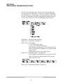
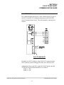
2.3 PACKET FORMAT FOR FULL DUPLEX PROTOCOL
The Data Link layer message packet always begins with “DLE STX”
and ends with “DLE ETX BCC” control symbols. These control
symbols, as well as “DLE Doubling”, are automatically added to the
users message packet as the frame is being prepared for transmission.
When a message packet is received, only the message is returned to
the user. All other unnecessary control symbols are removed.
Figure 2.1 shows the format of a typical message packet for Full
Duplex protocol.
Refer to the Allen-Bradley Data Highway/Data Highway Plus™/DH485 Communication Protocol and Command Set Reference Manual,
chapter 3.2 Message Packet Formats for the Basic Command Set, for
more information on formatting the message packet.
Figure 2.1 Packet Format for Full-Duplex Protocol
S4516-DF1 Program Development Manual
SYSTEMS Electronics Group
-6-
SECTION 2
DEVELOPING THE MESSAGE PACKET
2.4 HOW THE TRANSMITTER OPERATES
When transmitting a message packet the S4516-DF1 will first search
the data string for any DLE characters (10 HEX), and initiate “DLE
Doubling”. It will then attach the necessary starting and ending
control symbols and calculate the block check character, BCC. Once
assembled, the message packet is transmitted, typically to a Data Link
or some other RS232 interface. When the transmission is complete,
the S4516-DF1 waits for a reply indicating receipt of the message.
Once a response is returned the S4516-DF1 will return with a
“DONE”.
Under normal operation a two byte data string acknowledging the
receipt of the message will be returned indicating the success of the
delivery. The S4516-DF1 will automatically retry the message up to 3
times if the communication interface is not responding and up to 10
times if a request for retransmission, DLE ENQ, is returned. If the
transmission was not successful, the S4516-DF1 will return with
“DONE” indicating a problem with the transmission.
System function sfunc11() will be used to transmit the users message
packet to another node on the Allen-Bradley Data Highway. The
format and function of the sfunc11() has not changed, however, the
“Source” data will now contain the message packet to be delivered.
The message packet is developed within the users main program
code.
See section 2.6 “Message Packet Formats”, for additional information
on developing an Application Data message packet.
S4516-DF1 Program Development Manual
SYSTEMS Electronics Group
-7-
SECTION 2
DEVELOPING THE MESSAGE PACKET
2.5 HOW THE RECEIVER OPERATES
The receiver continually scans for incoming data. Once the start of
transmission, DLE STX, control symbol is received, a message packet
is assembled and the receiver looks for instances of “DLE Doubling”
and removes any additional DLE characters.
Once the end of transmission, DLE ETX BCC, control symbol has
been received, the “Block Check Character, BCC, is verified. If the
BCC received is valid, a two byte data string acknowledging the
message is transmitted back and the message packet is copied into the
sfunc10() receive buffer. However if the BCC is not valid, a data
string, not acknowledging the message is transmitted back and the
message packet is not returned to the user.
System function sfunc10() should be continually called from the users
program. As with system function sfunc11(), the format and function
have not been changed. However, when a valid message is received,
the entire packet, along with the size in bytes, is returned with all the
unnecessary formatting and framing control symbols removed. See
section 2.6 “Message Packet Formats”, for additional information.
2.6 MESSAGE PACKET FORMATS
This section provides two examples for developing message packet
formats for the PLC5 and SLC500 family processor commands.
Please refer to the Allen-Bradley Data Highway/Data Highway
Plus™/DH-485 Communication Protocol and Command Set
Reference Manual, Unit III: Application Layer Message Packet
Fields, for more information on formatting the message packet.
The S4516-DF1 embedded DF1 driver offers a large flexibility when
developing message packets to communicate with other AllenBradley PLC processors. The sample code that accompanies this
manual demonstrates only a few ways to develop message packet
formats.
The following sections provide the most common message formats
for reading and writing data to PLC5 and SLC500 processors.
S4516-DF1 Program Development Manual
SYSTEMS Electronics Group
-8-
SECTION 2
DEVELOPING THE MESSAGE PACKET
2.6.1 PLC5 WORD RANGE READ/WRITE
The “Word Range Read (Read Block)” or “Word Range Write (Write
Block)” are good message packet formats for reading or writing data
to a PLC5 processor. The starting address is either a logical binary
address or a logical ASCII address and must point to a word or a file.
Message Packet Format - Word Range Read:
An EXT STS (extended status) byte will replace the data field if there
is an error, STS (status byte) will not be zero.
Message Packet Format - Word Range Write:
An EXT STS (extended status) byte will be attached only if there is
an error, STS (status byte) will not be zero.
PACKET OFFSET and TOTAL TNS are in number of “Elements”.
DATA is in an even number of “Bytes”, (2 bytes = 1 element).
SIZE is number of “DATA Bytes”.
S4516-DF1 Program Development Manual
SYSTEMS Electronics Group
-9-
SECTION 2
DEVELOPING THE MESSAGE PACKET
The PLC5 System Address uses four levels of encoded addressing.
The first byte is the “Mask Byte”. This byte is required. Setting the
bits within this byte sets the number of levels and which levels will be
encoded. In the sample code that accompanies this manual, this byte
is set to 0fH. This sets 4 levels of encoded addressing as follows:
ADD Mask: Encoded Addressing Byte
ADD Level 1: Data Table - Default = 0
ADD Level 2: File Number
0 - 8 are Default File Types
9 - 999 are User Defined File Types
If this number is greater than 255, set this byte to FFH
which will allow the file number to be encoded into the
next two bytes.
Floating point are two words long (4 bytes).
ADD Level 3: Element Number - 0 through 999
If this number is greater than 255, set this byte to FFH
which will allow the element number to be encoded
into the next two bytes.
ADD Level 4: Sub-Element Number - Default = 0
S4516-DF1 Program Development Manual
SYSTEMS Electronics Group
-10-
SECTION 2
DEVELOPING THE MESSAGE PACKET
2.6.2 SLC500 PROTECTED TYPED LOGICAL READ/WRITE
The “Protected Typed Logical Read” or “Protected Typed Logical
Write” are good message packet formats for reading or writing data to
a SLC500 processor.
Message Packet Format - Protected Typed Logical Read
with Three Address Fields:
An EXT STS (extended status) byte will replace the data field if there
is an error, STS (status byte) will not be zero.
Message Packet Format - Protected Typed Logical Write
with Three Address Fields:
An EXT STS (extended status) byte will be attached only if there is
an error, STS (status byte) will not be zero.
S4516-DF1 Program Development Manual
SYSTEMS Electronics Group
-11-
SECTION 2
DEVELOPING THE MESSAGE PACKET
In these message packet formats the CMD, STS, TNS and FNC fields
perform the same typical functions. However, the remaining fields
are described below:
Field
Byte Size:
Description
The size of data to be read (in bytes), not including
the address fields or other overhead bytes.
File Number:
This byte addresses files 0-254 only. For higher
addresses, setting this byte to FF expands this field
to three bytes total. Use the second and third bytes
for the expanded file address (low address byte
first).
File Type:
Warning: You must use one of the following
values for this field. Do no use any other values;
doing so may result in unpredictable results.
80-83 HEX: Reserved
84 HEX: Status
85 HEX: Bit
86 HEX: Timer
87 HEX: Counter
88 HEX: Control
89 HEX: Integer
Element Number: This byte addresses elements 0-254 only. For
higher addresses, setting this byte to FF HEX
expands this field to three bytes total. Use the
second and third bytes for the expanded element
address (last address byte first).
Sub-Element:
This byte addresses elements 0-254 only. For
higher addresses, setting this byte to FF HEX
expands this field to three bytes total. Use the
second and third bytes for the expanded element
address (last address byte first).
S4516-DF1 Program Development Manual
SYSTEMS Electronics Group
-12-
SECTION 3
USING THE SYSTEM FUNCTIONS
This section describes using the system functions sfunc10/11/13 for
the S4516-DF1. Refer to the M4500 Program Development manual
for more detailed information.
The sfunc10/11 are no longer used for general purpose User Port
communications. The sfunc10() and sfunc11() are used to receive
and transmit data utilizing the embedded Allen-Bradley DF1 full
duplex protocol.
The format is the same, however, the function has changed. Refer to
the M4500 Program Development Manual, Section 5, “Programming
Language Reference”, for more information on “System Functions”.
3.1 INITIALIZING THE S4516-DF1 FOR COMMUNICATIONS
S4516-DF1 is initialized for communications using system function
sfunc19(). This is typically done in the initialization file of the
M4500
The following code is an example of how to initialize the S4516-DF1
for communications (S4516-DF1 board located in slot02).
W8156 = 7552;
sfunc19(1,3,1);
/* S4516-DF1 Located in slot-02 */
/* S4516-DF1 S3000 Network Node 1 */
/* S3000 Network Baud Rate = 344k */
/* User Port Baud Rate = 19200 */
If the S4516-DF1 were to be used as a slave on the S3000 network the
board would need to be initialized using the following code.
B161.6 = 1;
W8154 = 7552;
W8156 = W8154;
sfunc19(1,3,1);
/* sfunc13 Slave mode Enabled */
/* Slave slot Address for sfunc13 slave mode */
/* S4516-DF1 Located in slot-02 */
/* Initialize S4516-DF1 Board */
/* S3000 Network Node 1 */
/* S3000 Network Baud Rate = 344k */
/* User Port Baud Rate = 19200 */
S4516-DF1 Program Development Manual
SYSTEMS Electronics Group
-13-
SECTION 3
USING THE SYSTEM FUNCTIONS
3.2 RECEIVING THROUGH THE USER PORT (sfunc10)
The sfunc10 will perform the following functions:
• Receives message packets
• Check for transmission errors using the Block Check Character,
BCC, method.
• Removes the starting and ending control symbols and any
unnecessary DLE characters.
• Returns a response upon receipt of the message packet.
General Form:
sfunc10(#max,dest);
Parameters:
#max: This number is essentially ignored by the
sfunc10 call and should be set to 250 which
is the maximum number of bytes that can
be returned.
dest:
This is the address of the first byte of the
sfunc10 receive buffer. The receive buffer
is where the message packet will be copied
to from the S4516-DF1. Variable types:
“B” or indirect “*B”.
Return Value: The return value is the total number of bytes contained
within the message packet. Therefore whenever a
message packet is received the format will always be
the same. These bytes are as follows:
[DST] [SRC] [CMD] [STS] [TNS (2-bytes)] [DATA]
Type:
Simultaneous.
Valid Files:
Initialization, Main Program and User Functions.
S4516-DF1 Program Development Manual
SYSTEMS Electronics Group
-14-
SECTION 3
USING THE SYSTEM FUNCTIONS
3.3 TRANSMITTING THROUGH THE USER PORT (sfunc11)
The sfunc11 will perform the following functions:
• Assemble the message packet by attaching the starting and ending
control symbols and inserting additional DLE characters as
needed.
• Transmit the message packet.
• Wait for an acknowledge of receipt of transmission.
• Retry the message if the transmission is unsuccessful.
• Return with a response indicating the success of the transmission.
General Form:
sfunc11(#sent,srce);
Parameters:
#sent: The number of bytes to transmit out the
User Port.
Variable Types: Constant (1-250), “B” or
indirect “*B”.
scre:
The address where the first byte transmitted
is stored. A consecutive number of bytes
(= #sent) is transmitted out the USERPORT
starting with this address. Variable types:
“B” or indirect “*B”.
Return Values:
0 = Not Busy, Ready.
1 = Busy.
2 = Done - “DLE ACK” Received.
3 = Done - Error, “DLE NAK” Received.
4 = Done - Error, “DLE ENQ” Time Out.
5 = Done - Error, No Response Time Out.
6 = Done - Error, Packet too Large.
Type:
Simultaneous.
Valid Files:
Initialization, Main Program and User Functions.
S4516-DF1 Program Development Manual
SYSTEMS Electronics Group
-15-
SECTION 3
USING THE SYSTEM FUNCTIONS
3.4 COMMUNICATING ON THE S3000 NETWORK (sfunc13)
System function sfunc13 is used to communicate to other S3012s,
S3014s, M4000 modules, or other M4500 nodes on the S3000 serial
communications network. The operation of the sfunc13 is identical to
that described in the “M4500 Program Development Manual”.
S4516-DF1 Program Development Manual
SYSTEMS Electronics Group
-16-
SECTION 4
PLC5 TO S4516-DF1
COMMUNICATION GUIDE
4.1 HARDWARE
DF1 communications takes place via the Channel 0 port (25-pin) of
the PLC5 to the RS-232 communications port on the S4516-DF1
Serial Communications board. The cable should be constructed as
follows:
PLC5 TO S4516-DF1
Internally, the PLC5 should be setup for RS-232 communications.
Refer to the dip switch setting guide on the side of the processor.
Additionally, Dip switch SW1 on the S4516-DF1 board is the RS232/RS-422 dip switch and should be set as follows:
POLE 1 = ON
POLE 2 = off
S4516-DF1 Program Development Manual
SYSTEMS Electronics Group
-17-
SECTION 4
PLC5 TO S4516-DF1
COMMUNICATION GUIDE
Dip switch SW2 is the slot address. This is dependent upon the rest
of the cards in the M4500 rack. In the above example, the board is
setup for slot01 (POLE 1 = ON, POLE 2 = off).
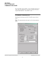
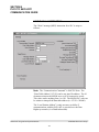
4.2 CHANNEL 0 CONFIGURATION
The Channel 0 Serial port on the PLC5 should be setup as shown
below.
Note: The communication mode must be set for System (point-topoint).
S4516-DF1 Program Development Manual
SYSTEMS Electronics Group
-18-
SECTION 4
PLC5 TO S4516-DF1
COMMUNICATION GUIDE
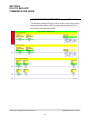
The Channel 0 “Options” are set as follows:
Note: The “Detect Duplicate Messages” should be unchecked.
S4516-DF1 Program Development Manual
SYSTEMS Electronics Group
-19-
SECTION 4
PLC5 TO S4516-DF1
COMMUNICATION GUIDE
4.3 USING THE MSG INSTRUCTION (sample PLC code)
The following sample RSLogix5 code is used to execute the message
control function to allow a PLC5 to communicate with the S4516DF1 Serial Communications board.
S4516-DF1 Program Development Manual
SYSTEMS Electronics Group
-20-
SECTION 4
PLC5 TO S4516-DF1
COMMUNICATION GUIDE
4.4 THE “READ” INSTRUCTION
The “Read” message (MSG) instruction for a PLC5 is setup as
follows:
Note: The “Communication Command” is PLC3 Word Range Read.
The “Data Table Address” (N7:0) can be any inter file address. The
50 elements read from the M4500 are a set of 50 consecutive words.
This value can be anything from 1 to 120. The M4500 PLC code can
be written to interpret the data table address (i.e. N7:0 = W4300).
The “Local Station Address” is only necessary to define if
communications with the S4516-df1 is executed over the Data
Highway network (via a DataLink module).
S4516-DF1 Program Development Manual
SYSTEMS Electronics Group
-21-
SECTION 4
PLC5 TO S4516-DF1
COMMUNICATION GUIDE
4.5 THE “Write” INSTRUCTION
The “Write” message (MSG) instruction for a PLC5 is setup as
follows:
Note: The “Communication Command” is PLC3 Word Range Write.
The “Data Table Address” (N7:50) can be any inter file address. The
10 elements written to the M4500 are a set of 10 consecutive words.
This value can be anything from 1 to 120. The M4500 PLC code can
be written to interpret the data table address (i.e. N7:50 = W4400).
The “Local Station Address” is only necessary to define if
communications with the S4516-df1 is executed over the Data
Highway network (via a DataLink module).
S4516-DF1 Program Development Manual
SYSTEMS Electronics Group
-22-
SECTION 5
SLC500 TO S4516-DF1
COMMUNICATION GUIDE
5.1 HARDWARE
DF1 communications takes place via the Channel 0 port (95-pin) of
the SLC500 to the RS-232 communications port on the S4516-DF1
Serial Communications board. The cable should be constructed as
follows:
SLC500 TO S4516-DF1
Additionally, Dip switch SW1 on the S4516-DF1 board is the RS232/RS-422 dip switch and should be set as follows:
POLE 1 = ON
POLE 2 = off
Dip switch SW2 is the slot address. This is dependent upon the rest
of the cards in the M4500 rack. In the above example, the board is
setup for slot01 (POLE 1 = ON, POLE 2 = off).
S4516-DF1 Program Development Manual
SYSTEMS Electronics Group
-23-
SECTION 5
PLC5 TO S4516-DF1
COMMUNICATION GUIDE
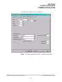
5.2 CHANNEL 0 CONFIGURATION
The Channel 0 Serial port on the PLC5 should be setup as shown
below.
Note: The communication mode must be set for System (point-topoint).
S4516-DF1 Program Development Manual
SYSTEMS Electronics Group
-24-
SECTION 5
SLC500 TO S4516-DF1
COMMUNICATION GUIDE
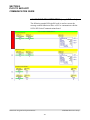
The Channel 0 “Options” are set as follows:
Note: The “Detect Duplicate Messages” should be unchecked.
S4516-DF1 Program Development Manual
SYSTEMS Electronics Group
-25-
SECTION 5
PLC5 TO S4516-DF1
COMMUNICATION GUIDE
5.3 USING THE MSG INSTRUCTION (sample PLC code)
The following sample RSLogix500 code is used to execute the
message control function to allow a SLC to communicate with the
S4516-DF1 Serial Communications board.
S4516-DF1 Program Development Manual
SYSTEMS Electronics Group
-26-
SECTION 5
SLC500 TO S4516-DF1
COMMUNICATION GUIDE
5.4 THE “READ” INSTRUCTION
The “Read” message (MSG) instruction for a SLC is setup as follows:
Note: The “Communication Command” is 500CPU Read. The
“Data Table Address” (N7:0) can be any inter file address. The 50
elements read from the M4500 are a set of 50 consecutive words.
This value can be anything from 1 to 120. The M4500 PLC code can
be written to interpret the data table address (i.e. N7:0 = W4300).
The “Local Station Address” is only necessary to define if
communications with the S4516-df1 is executed over the Data
Highway network (via a DataLink module).
S4516-DF1 Program Development Manual
SYSTEMS Electronics Group
-27-
SECTION 5
PLC5 TO S4516-DF1
COMMUNICATION GUIDE
5.5 THE “Write” INSTRUCTION
The “Write” message (MSG) instruction for a SLC is setup as
follows:
Note: The “Communication Command” is 500CPU Write. The
“Data Table Address” (N7:50) can be any inter file address. The 10
elements written to the M4500 are a set of 10 consecutive words.
This value can be anything from 1 to 120. The M4500 PLC code can
be written to interpret the data table address (i.e. N7:50 = W4400).
The “Local Station Address” is only necessary to define if
communications with the S4516-df1 is executed over the Data
Highway network (via a DataLink module).
S4516-DF1 Program Development Manual
SYSTEMS Electronics Group
-28-
SECTION 6
CONFIGURING THE DATA LINK
The following instructions are provided as a guideline for setting up
the Data Link DL2000 to operate with the S4516-DF1
communications board. For more information, refer to the
DATALINK DL2000 Communication Controller User’s Guide.
With power applied, perform the following to configure the Data Link
DL2000.
• With the DL97 Data Link Configuration software running, select
the “FREESTANDING UNIT - DL2000 ALL MODELS” option
and then click the “LAUNCH DL97 CONFIGURATION
SOFTWARE FOR A FREESTANDING UNIT” command button.
• Then select the “FREESTANDING” model to be configured, i.e.
“DL2000-K2F” - Two Serial Interface Ports to A-B DH+.
• Select the “COM PORT” that the computer will be using to
interface with the Data Link and make sure the serial
communications cable is connected.
• Within the “DATALINK OPERATING PARAMETERS”, click
the “CONFIGURE PARAMETERS” command button.
• Under the “OPERATING MODE SELECTION”, select the
“STANDARD DF1 TO DH+” option.
• Set the “STATION NUMBER” to the next available node on the
network.
• Set the “NETWORK SPEED”. Typically this is set to 57.6k
baud.
• Set the “CHANNEL SERIAL SPEED”. This is the speed at
which the S4516-DF1 will communicate to the Data Link. If
using the S4516-DF1 in conjunction with the S3000 network set
the speed to 9600 baud, otherwise it can be set to either 9600 or
19.2k baud.
• Click the “SET ADVANCED DF1 PROTOCOL
PARAMETERS” command button.
• Under the “DUPLICATE MESSAGE”, select the “ACCEPT”
option and click the “ACCEPT” command button.
• Then click the “NEXT - TO DOWNLOAD TO DL” command
button at the bottom of the screen
• Then click “CLICK HERE TO DOWNLOAD PARAMETERS
TO DL” command button. Follow the instructions to place the
Data Link into a “Configuration Mode”, and download the
parameters.
• Then return to the “Welcome Screen”.
• Then “QUIT DL97”.
• Press the “Reset” to put the Data Link on line.
S4516-DF1 Program Development Manual
SYSTEMS Electronics Group
-29-
SECTION 6
CONFIGURING THE DATA LINK
(This Page Intentionally Left Blank)
S4516-DF1 Program Development Manual
SYSTEMS Electronics Group
-30-
APPENDIX A
ASYNCHRONOUS LINK STATUS CODES
Local STS Error Codes:
Code (HEX):
00
01
02
03
04
05
06
07
08
Definition:
Success - No Error
Not Used
Cannot Guarantee Delivery: Link Layer
Duplicate Token Holder Detected
Local Port is Disconnected
Application Layer Timed out waiting for a
response
Duplicate Node Detected
Station is Off-Line
Hardware Fault
Remote STS Error Codes:
Code (HEX):
00
10
20
30
40
50
60
70
80
90
A0
B0
C0
D0
E0
F0
Definition:
Success - No Error
Illegal Command or Format
Host has a Problem and Will Not Communicate
Remote Node Host is Missing, Disconnected or
Shut Down
Host Could Not Complete Function Due to
Hardware Fault
Addressing Problem or Memory Protect Rungs
Function Disallowed due to Command
Protection Selection
Processor is in Program Mode
Compatibility Mode File Missing or
Communication Zone Problem
Remote Node Cannot Buffer Command
Not Used
Remote Node Problem Due to Download
Cannot Execute Command Due to Active IPBs
Not Used
Not Used
There is an Error Code in the EXT STS Byte
S4516-DF1 Program Development Manual
SYSTEMS Electronics Group
- A-1 -
APPENDIX A
ASYNCHRONOUS LINK STATUS CODES
EXT STS Codes for Command Code 0E (HEX):
Code (HEX):
0
1
2
3
4
5
6
7
8
9
A
B
C
D
E
F
10 to 1F
20
21
22
23
24
25
26
27
28
29
2A
Definition:
Multi-Defined Processors on Ring
Processor is Already Allocated
Processor must be Allocated for this Command
Extended Function in Progress
Extended Function in Progress
Function Not Available in this Processor
Command Set
Function Not Available in this Processor Mode
Processor Number in Program and Hardware
Do Not Match
Invalid Address
Memory Protection Access Violation
Invalid Parameter
Search Unsuccessful
Program Needs to be Stored - RAM and PROM
Do Not Match
External EEPROM is Defective, Cannot
transfer Contents Correctly
Invalid User Program
Not Used
Device Resource Unavailable
Not Used
Processor Already Allocated by requesting
Node
Processor Already Allocated by Another
Remote Node.
Processor Not Allocated
Data Length Invalid
Data Size Too Large
Data Size Too Large
Data Size Too Small
At Least One of the Addresses Points to a
Read-Only Area
Address Past End of Memory
Memory Protected, Addresses to Program Area
Illegal
Memory Protected, Address to Processor Status
Area Illegal
S4516-DF1 Program Development Manual
SYSTEMS Electronics Group
- A-2 -
APPENDIX A
ASYNCHRONOUS LINK STATUS CODES
EXT STS Codes for Command Code 0E (HEX) (cont.):
Code (HEX):
2B
2C
2D
2E
2F
30 to 7B
7C
7D
7F
80 to FF
Definition:
Memory Protected, Address to Protected Timer
or Counter
Processor Not in Program Mode, Address to
Program Area.
Address Past “End of Used Memory”
“Program Valid” Bit Not Set in PLC4 Program
ID Byte
Invalid PLC4 Select Value
Not Used
PLC4 Ring Disconnected
No PLC4 Response
Invalid PLC4 Selected Byte
Not Used
S4516-DF1 Program Development Manual
SYSTEMS Electronics Group
- A-3 -
APPENDIX A
ASYNCHRONOUS LINK STATUS CODES
EXT STS Codes for Command Code 0F (HEX):
Code (HEX):
0
1
2
3
4
5
6
7
8
9
A
B
C
D
E
F
10
11
12
13
14
15
16
17
18
19
1A
1B
1C to FF
Definition:
Not Used
A Field Has an Illegal Value
Less Levels Specified in Address than
Minimum for an Address
More Levels Specified in Address than System
Supports
Symbol Not Found
Symbol is of Improper Format
Address Doesn’t Point to Something Usable
File is Wrong Size
Cannot Complete Request, Situation has
Changed Since the Start of the Command
Data or File is Too Large
Transaction Size Plus Word Address is too
Large
Access Denied, Improper Privilege
Condition Cannot be Generated - Resource is
Not Available
Condition Already Exists - Resource is Already
Available
Command Cannot be Executed
Histogram Overflow
No Access
Illegal Data Type
Invalid Parameter or Invalid Data
Address Reference Exists to Deleted Area
Command Execution Failure for Unknown
Reason; Possible PLC3 Histogram Overflow
Data Conversion Error
Scanner Not Able to Communicate with 1771
rack adapter
Adapter Cannot Communicate with Module
1771 Module Response was not valid
Duplicated Label
File is Open; Another Node Owns it
Another Node is the Program Owner
Not Used
S4516-DF1 Program Development Manual
SYSTEMS Electronics Group
- A-4 -
APPENDIX B
SAMPLE SYSdev PROGRAM CODE
S4516-DF1 Serial Communications - Sample Program Code
SYS96 Init file: C:\PROGRAMS\AB_DF1\DF1_MAIN.LIN
02/07/02
-- DF1_MAIN.R01
Initial Release: 08/1999
Revised:
02/2000
Systems Electronics Group
-- The S4516-DF1 is an application specific serial communications
board that has been embeded with the Allen-Bradley DF1 communication
protocol.
This allows the M4500 PLC to reside as a node on the Allen-Bradley
Data Highway network. Communication to the Data Highway is done
through a Datalink Communication Controller.
The S4516-Df1 can be setup to communicate to the Datalink at either
9600 baud or 19.2 kbaud. At the same time the S4516-DF1 can
communicate across the S3000 network allowing for seemless
integration of two networks.
The following sample code is an example of how to read and write
data to and Allen-Bradley PLC5 or SLC500. The code can be used
"As Is" with very few modifications or, if so desired, completely
modify this program to suit the users needs.
The embeded DF1 driver uses sfunc11() to transmit the message packets
to the Datalink and sfunc10() to receive. There are no changes in
the format of these two system functions.
When transmitting a message packet the DF1 driver will attach the
necessary control symbols and send the data to the Datalink and
return with a "DONE" when finished transmitting.
When receiving data, unnecessary control symbols are stripped from
the data stream so that only the raw message packet is returned to
the user.
This allows for a great deal of flexability when sending and
receiving message packets with an Allen-Bradley PLC.
This program uses the following variables:
B3000 - B3025: Main Program Control Bytes.
B3050 - B3299: sfunc11() Send Buffer.
B3300 - B3549: sfunc10() Receive Buffer.
S4516-DF1 Program Development Manual
SYSTEMS Electronics Group
- B-1 -
APPENDIX B
SAMPLE SYSdev PROGRAM CODE
SYS96 Init file: C:\PROGRAMS\AB_DF1\DF1_MAIN.LIN
**************************************************************************
block: 1 - High-level
0:/* Initialize S4516 Board */
1:W8154 = &W7552;
/* Slot Address for sfunc13 */
2:W8156 = &W7552;
/* S4516DF1 Slot Address (02), for sfunc10/11 */
3:B3023 = sfunc19(1,3,1); /* sta_addr=1, net_buad=344k, user_baud=19200 */
4:B161 = 40H;
/* Enable Slave Response Mode */
5:
6:/* Initialize DF1 Presets */
7:W3000 = 0;
/* Clear DF1 Control Bits */
8:B3000.2 = 1;
/* Set = 1 to Initiate Command Message Packet */
9:B3010 = 110;
/* Num of Elements (Read/Write) = 110 */
10:B3011 = 7;
/* File Number = N7 */
11:W3012 = 40;
/* Starting Element = 40 */
12:W3016 = 1;
/* Initialize TNS Counter */
13:W3018 = 0;
/* Clear Error Code */
14:B3024 = 100;
/* Initialize Timeout Timer Preset (~10sec) */
15:B3025 = B3024;
/* Initialize Timeout Timer Accumulator */
16:
B0161 (SysEnFl)
B3000.2(RespPnd)
B3010 (NumElem)
B3011 (FileNum)
B3023 (sf11Rtn)
B3024 (~RespPr)
B3025 (~RespAc)
W3000 (CtrlBts)
W3012 (StrtElm)
W3016 ( TNS )
W3018 ( STS )
W7552 (SlotAdd)
W8154 (SlotAdd)
W8156 (SlotAdd)
System
Waiting
Num of
A/B
sfunc19
No Resp
No Resp
DF1
Startng
AppData
Error
4516DF1
sfunc13
sfunc10
Enable
for
Elemnts
Target
Respons
TimeOut
TimeOut
Control
Element
TNS
Code
Slot
Slave
/11/13
Flags
Respons
FileNum
Code
Preset
Acum.
Bits
STS
Address
SlotAdd
SlotAdd
S4516-DF1 Program Development Manual
SYSTEMS Electronics Group
- B-2 -
APPENDIX B
SAMPLE SYSdev PROGRAM CODE
SYS96 Main Program: C:\PROGRAMS\AB_DF1\DF1_MAIN.LMN
**************************************************************************
block: 1 - High-level
0:ufunc01();
1:
/* Call DF1_comm() */
S4516-DF1 Program Development Manual
SYSTEMS Electronics Group
- B-3 -
APPENDIX B
SAMPLE SYSdev PROGRAM CODE
SYS96 User function 1: C:\PROGRAMS\AB_DF1\DF1_MAIN.L01
DF1_comm(); User Function File:
-- This user funcion file handles the transmitting and receiving
of Application Data to a Datalink Communications Module.
B3000 - B3025: Main Program Control Bytes.
B3050 - B3299: sfunc11() Send Buffer.
B3300 - B3549: sfunc10() Receive Buffer.
NOTE: This code can be used as either a "Command Initiator" (master)
or a "Command Receiver" (slave) without any modification to the
code.
-- ufunc02() - DF1_AppData(), is called from this user function file
to assemble the Application Data packet. B3014 determines which
APP DATA packet will be assembled. This allows the user to generate
any number of different APP DATA packets to be transmitted to the
Datalink.
-- Once an APP DATA packet has been assembled, sfunc11 formats the frame
and transmits the data to the Datalink and then returns the
appropriate response code. If the packet sent was a "Command
Initiator" then a reply should be expected. If a reply is not
returned within a period of time, the transaction number (TNS) is
incremented and the message resent.
-- sfunc10 is continuously called from this user function. This system
function returns only the APP DATA received from the Datalink with
all formating and framing characters removed.
The command (CMD) and function (FCN) bytes, together define the
activity to be performed
-- This sample code will allow data to be read or written to a PLC5 or
SLC500 based on the following message packet formats:
1)
2)
3)
4)
PLC5 PLC5 SLC500
SLC500
Word Range Read (Read Block)
Word Range Write (Write Block)
- Protected Typed Logical Read with Three Address Fields
- Protected Typed Logical Write with Three Address Fields
Refer to the Allen-Bradley, Data Highway/Data Highway Plus(TM)/
DH-485 Communication Protocol and Command Set Reference Manual,
Unit III: Application Layer Message Packet Fields for more
information.
S4516-DF1 Program Development Manual
SYSTEMS Electronics Group
- B-4 -
APPENDIX B
SAMPLE SYSdev PROGRAM CODE
SYS96 User function 1: C:\PROGRAMS\AB_DF1\DF1_MAIN.L01
**************************************************************************
block: 1 - High-level
DF1_comm(); User Function File:
-- This block is used to transmit and receive APP DATA from the
Datalink.
-- Transmitting Data:
B3000.0 is set when a message packet is to be delivered to the
Datalink. Once sfunc11 is "DONE", this bit is reset, as well as,
B169.1. Clearing B169.1 allows the sfunc11 response codes to be
returned, these are as follows:
1:
2:
3:
4:
5:
6:
Busy
Done
Done
Done
Done
Done
-
DLE ACK Received (Message Acknowledged)
DLE NAK Received (Message Not Acknowledged)
DLE ENQ Timeout (Request for Retransmission Timeout)
No Response Timeout from Datalink
Message Packet Too Large to Transmit (> 250 Bytes)
If something other than a "2" is returned, the message packet is
sent again. Additional code could be inserted to keep track of the
number of times an error code is returned and then take appropriate
action.
B3000.1, if set, allows user function ufunc02(), DF1_AppData(), to be
called which will assemble a "Command" Message Packet.
B3000.2, if set, flags the system to expect a response from a
"Command" Message Packet. This enables the "No Response Timeout"
timer to resend the message packet if a reply is not received.
W1500 through W1748 (250 bytes), are used as a "Read Data" buffer.
This should be modified to suit the users needs.
W1750 through W1998 (250 bytes), are used as a "Write Data" buffer.
This should be modified to suit the users needs.
-- Receiving Data:
System function sfunc10() is used to retrieve data sent from the
Datalink. The entire message packet is returned with all the
necessary transmission symbols removed.
Bit 6 of the Command byte (B3302) is the command/reply indicator.
B3302.6 is set to a "0" in a command message packet and set to a "1"
in a reply message packet.
S4516-DF1 Program Development Manual
SYSTEMS Electronics Group
- B-5 -
APPENDIX B
SAMPLE SYSdev PROGRAM CODE
0:/* Transmit APP DATA to Data Link */
1:if (B3000.0 == 1)
/*
2:
{
/*
3:
if (B3000.1 == 1)
/*
4:
ufunc02();
/*
5:
B3021 = sfunc11(B3015, B3050);
/*
6:
if (B3021 > 1)
/*
7:
{
/*
8:
B169.1 = 0;
/*
9:
B3000.0 = 0;
/*
10:
B3022 = B3021;
/*
11:
if (B3021 == 2)
/*
12:
{
/*
13:
if (B3000.1 == 1)
/*
14:
{
/*
15:
B3000.1 = 0;
/*
16:
B3000.2 = 1;
/*
17:
}
18:
}
19:
else
/*
20:
B3000.0 = 1;
/*
21:
}
22:
}
23:
24:
25:/* Receive APP DATA from Data Link */
26:B3020 = sfunc10(250, B3300);
/*
27:if (B3020 > 0)
/*
28:
{
/*
29:
if (B3302.6==0)
/*
30:
B3000.3 = 1;
/*
31:
else
/*
32:
B3000.4 = 1;
/*
33:
}
34:
B0169.1(sf11ErE)
B3000.0(XmitPkt)
B3000.1(CMDInit)
B3000.2(RespPnd)
B3000.3(CMD=CMD)
B3000.4(CMD=Rpy)
B3015 (sf11Sen)
B3020 (sf10Rtn)
B3021 (sf11Rtn)
B3022 (sf11_Pv)
B3050 (App_DST)
B3300 (App_DST)
THRU
B3302.6(CMD/Rpy)
B3549 (AppDATA)
sfunc11
Xmit
Command
Waiting
Recievd
Recievd
sfunc11
sfunc10
sfunc11
sfunc11
AppData
AppData
ErrCode
AppData
Init.
for
CMD=CMD
CMD =
#sent
NumByte
Respons
Respons
Send
Receive
Xmit APP DATA Packet? */
Yes */
Command Initiator? */
Assemble APP DATA Packet */
Transmit APP DATA Packet */
Done? */
Yes */
Reset B169.1 - MANDITORY */
Reset Xmit APP DATA */
Save Xmit Response */
"DLE ACK" Received? */
Yes */
Command Initiator Set? */
Yes */
Reset Command Initiator */
Set Response Pending */
"DLE ACK" Not Received */
Resend APP DATA Packet */
Receive Data From S4516DF1 */
Message Received? */
Yes - Decipher Command Bit */
CMD == Command? */
Set CMD = Command */
CMD == Reply */
Set CMD = Reply */
Enable
Packet
Respons
Reply
Return
Code
Prev.
DST
DST
Command /Reply Indictr
AppData Receive DATA
S4516-DF1 Program Development Manual
SYSTEMS Electronics Group
- B-6 -
APPENDIX B
SAMPLE SYSdev PROGRAM CODE
SYS96 User function 1: C:\PROGRAMS\AB_DF1\DF1_MAIN.L01
**************************************************************************
block: 2 - High-level
DF1_comm(); User Function File:
-- This block sets up the reply message packet to respond to a command
message received.
All command message packets received will have the same basic reply
message packet format. The following is typical for a "Write"
function command:
[DST][SRC][CMD][STS][TNS-LO][TNS-HI]
If the function received is a "Read" command then message packet will
have the following format:
[DST][SRC][CMD][STS][TNS-LO][TNS-HI][ - DATA - ]
If the starting address is outside the defined limits, the reply
message packet will have the following format:
[DST][SRC][CMD][STS][TNS-LO][TNS-HI][EXT STS]
Where the EXT STS byte will contain the value 06H - "Address Doesn't
Point to Something Usable"
The starting address should always be verified for proper range
because pointers are used to read and write data to memory within
the M4500.
NOTE:
When setting up Message Blocks the following elements will
determine the starting address in the M4500:
PLC5 - Message Control Block, Element 07
SLC500 - Message Control Block, Element 05
S4516-DF1 Program Development Manual
SYSTEMS Electronics Group
- B-7 -
APPENDIX B
SAMPLE SYSdev PROGRAM CODE
0:/*
1:if
2:
3:
4:
5:
6:
7:
8:
9:
10:
11:
12:
13:
14:
15:
16:
17:
18:
19:
20:
21:
22:
23:
24:
25:
26:
27:
28:
29:
30:
31:
32:
33:
34:
Command Message Packet Received */
(B3000.3 == 1)
{
B3000.0 = 1;
B3015 = 6;
B3050 = B3301;
B3051 = B3300;
B3052 = B3302 | 40H;
B3053 = 00H;
W3054 = W3304;
if (B3306==01H || B3306==00H)
{
if (B3310 == ffH)
B3006=B3316, B3007=B3315;
else
B3006=B3314, B3007=B3313;
}
else if (B3306==a2H || B3306==aaH)
{
if (B3310 == ffH)
B3006=B3311, B3007=B3312;
else
B3006=B3310, B3007=0;
}
else
;
if (W3006 < &W1500 || W3006 > &W1750)
{
B3000.3 = 0;
B3015 = 7;
B3053 = f0H;
B3056 = 06H;
}
}
B3000.0(XmitPkt)
B3000.3(CMD=CMD)
B3006 (Pointer)
B3007 (Pointer)
B3015 (sf11Sen)
B3050 (App_DST)
B3051 (App_SRC)
B3052 (App_CMD)
B3053 (App_STS)
B3056 (App_FCN)
B3300 (App_DST)
THRU
W1500 (DataSen)
W1750 (DataRcv)
W3006 (Pointer)
W3054 (App_TNS)
W3304 (App_TNS)
Xmit
Recievd
Pointer
Pointer
sfunc11
AppData
AppData
AppData
AppData
AppData
AppData
/*
/*
/*
/*
/*
/*
/*
/*
/*
/*
/*
/*
/*
/*
/*
CMD == Command */
Yes */
Set Send Message Packet */
Num of Bytes to Return */
DST = SRC */
SRC = DST */
CMD = Reply */
STS = 00H */
TNS = TNS Recieved */
PLC5 "Read" or "Write"? */
Yes */
Encoded Element ADD? */
Yes - Assign ADD (Pointer) */
No */
Assign ADD (Pointer) */
/*
/*
/*
/*
/*
/*
SLC500 "Read" or "Write"? */
Yes */
Encoded Element ADD? */
Yes - Assign ADD (Pointer) */
No */
Assign ADD (Pointer) */
/*
/*
/*
/*
/*
/*
Address Out of Range? */
Yes */
Reset CMD = Command */
Num of Bytes to Return */
STS = Code in EXT STS */
EXT STS = Improper ADD */
AppData Packet
CMD=CMD
#sent
Send
Send
Send
Send
Send
Receive
W1500
Thru
W1750
Thru
Pointer
AppData Send
AppData Receive
DST
SRC
CMD
STS
FCN
DST
W1748
W1998
TNS
TNS LO
S4516-DF1 Program Development Manual
SYSTEMS Electronics Group
- B-8 -
APPENDIX B
SAMPLE SYSdev PROGRAM CODE
SYS96 User function 1: C:\PROGRAMS\AB_DF1\DF1_MAIN.L01
**************************************************************************
block: 3 - High-level
DF1_comm(); User Function File:
-- This block responds to a "Read" function command delivered either
from a PLC5 or a SLC500. The function will be deciphered and a
data block will be formated and added to the reply message packet.
FCN
--01H
a2H
Description
----------PLC5 - Word Range Read (Read Block)
SLC500 - Protected Typed Logical Read
NOTE:
B3306 = FCN Byte
B3307 = SIZE (bytes) - SLC500
B3309 = SIZE (words) - PLC5
0:/* PLC5 or SLC500 Read Mode Command */
1:if (B3000.3 == 1)
/* CMD == Command */
2:
{
/* Yes */
3:
if (B3306==01H || B3306==a2H)
/* FNC = PLC5 or SLC500 Read */
4:
{
/* Yes */
5:
B3000.3 = 0;
/* Reset CMD = Command */
6:
if (B3306 == 01H)
/* PLC5 - Word Range Read? */
7:
{
/* Yes */
8:
W3002 = B3309 * 2;
/* Set "FOR LOOP" Limit */
9:
B3015 = B3015 + B3002;
/* Set Data Bytes to Return */
10:
}
11:
else
/* SLC500 - Typed Logical Read? */
12:
{
/* Yes */
13:
B3015 = B3015 + B3307;
/* Set Data Bytes to Return */
14:
B3002 = B3307;
/* Set "FOR LOOP" Limit */
15:
}
16:
W3008 = &B3056;
/* Point to Data Buffer */
17:
for (B3004 = 0; B3004 < B3002; ++B3004)
18:
{
19:
*B3008 = *B3006;
/* Load APP DATA Packet */
20:
++W3006, ++W3008;
/* Increment Data Pointers */
21:
}
22:
}
23:
}
24:
B3000.3(CMD=CMD) Recievd CMD=CMD
B3002 (Temp(C)) Temp
(calc.)
B3004 (Temp(i)) Temp
(i)
B3006 (Pointer) Pointer
B3008 (Pointer) Pointer
B3015 (sf11Sen) sfunc11 #sent
B3056 (App_FCN) AppData Send
FCN
THRU
W3002 (Temp(C)) Temp
(calc.)
W3006 (Pointer) Pointer
W3008 (Pointer) Pointer
S4516-DF1 Program Development Manual
SYSTEMS Electronics Group
- B-9 -
APPENDIX B
SAMPLE SYSdev PROGRAM CODE
SYS96 User function 1: C:\PROGRAMS\AB_DF1\DF1_MAIN.L01
**************************************************************************
block: 4 - High-level
DF1_comm(); User Function File:
-- This block responds to a "Write" function command delivered either
from a PLC5 or a SLC500. The function will be deciphered and the
data written to memory as specified by the PLC, as long as the
M4500 address is within range.
FCN
--00H
aaH
Description
----------PLC5 - Word Range Write (Write Block)
SLC500 - Protected Typed Logical Write
NOTE:
W3312
W3314
W3316
W3318
0:/*
1:if
2:
3:
4:
5:
6:
7:
8:
9:
10:
11:
12:
13:
14:
15:
16:
17:
18:
19:
20:
21:
22:
23:
24:
25:
26:
27:
28:
29:
=
=
=
=
Start
Start
Start
Start
of
of
of
of
DATA
DATA
DATA
DATA
-
SLC500 (Element ADD Not Encoded)
SLC500 (Element ADD Encoded)
PLC5 (Element ADD Not Encoded)
PLC5 (Element ADD Encoded)
PLC5 or SLC500 Write Command */
(B3000.3 == 1)
/* CMD == Command */
{
/* Yes */
B3000.3 = 0;
/* Reset CMD = Command */
if (B3306==00H || B3306==aaH)
/* FCN = PLC5 or SLC500 Write */
{
/* Yes */
if (B3306 == 00H)
/* PLC5 - Word Range Write */
{
/* Yes */
W3002 = B3309 * 2;
/* Set "FOR LOOP" Limit (TOT TNS) */
if (B3310 == ffH)
/* Encoded Element ADD? */
W3008 = &W3318;
/* Point to Data Received */
else
/* No */
W3008 = &W3316;
/* Point to Data Received */
}
else
/* SLC500 - Typed Logical Write */
{
B3002 = B3307;
/* Set "FOR LOOP" Limit (size-bytes)*/
if (B3310 == ffH)
/* Element Encoded? */
W3008 = &W3314;
/* Point to Data Received */
else
/* Element not Encoded */
W3008 = &W3312;
/* Point to Data Received */
}
for (B3004 = 0; B3004 < B3002; ++B3004)
{
*B3006 = *B3008;
/* Write Data to Memory */
++W3006, ++W3008;
/* Increment Data Pointers */
}
}
}
S4516-DF1 Program Development Manual
SYSTEMS Electronics Group
- B-10 -
APPENDIX B
SAMPLE SYSdev PROGRAM CODE
B3000.3(CMD=CMD)
B3002 (Temp(C))
B3004 (Temp(i))
B3006 (Pointer)
B3008 (Pointer)
THRU
W3002 (Temp(C))
W3006 (Pointer)
W3008 (Pointer)
W3312 (AppDATA)
W3314 (AppDATA)
W3316 (AppDATA)
W3318 (AppDATA)
Recievd CMD=CMD
Temp
(calc.)
Temp
(i)
Pointer
Pointer
Temp
Pointer
Pointer
AppData
AppData
AppData
AppData
(calc.)
Receive
Receive
Receive
Receive
DATA
DATA
DATA
DATA
S4516-DF1 Program Development Manual
SYSTEMS Electronics Group
- B-11 -
APPENDIX B
SAMPLE SYSdev PROGRAM CODE
SYS96 User function 1: C:\PROGRAMS\AB_DF1\DF1_MAIN.L01
**************************************************************************
block: 5 - High-level
DF1_comm(); User Function File:
-- This block responsd to a reply message packet received. The STS
and EXT STS bytes are checked for any message packet errors. W3018
contains the STS and EXT STS error code information.
If the STS and EXT STS bytes indicate that no errors have occurred,
then action is taken to copy any data returned to memory and then
setup for the next command message packet to be delivered.
B3303 = STS Byte
B3306 = EXT STS Byte
W3306 = Start of DATA Received
Refer to the Allen-Bradley Data Highway/Data Highway Plus(TM)/
DH-485 Communication Protocol and Command Set Reference Manual,
Chapter 4.1: Asynchronous Link Status Codes, for more information
on local, remote and extended status error codes.
S4516-DF1 Program Development Manual
SYSTEMS Electronics Group
- B-12 -
APPENDIX B
SAMPLE SYSdev PROGRAM CODE
0:/*
1:if
2:
3:
4:
5:
6:
7:
8:
9:
10:
11:
12:
13:
14:
15:
16:
17:
18:
19:
20:
21:
22:
23:
24:
25:
26:
27:
28:
29:
30:
31:
32:
33:
34:
35:
36:
M4500 Reply Message Packet */
(B3000.4 == 1)
{
B3000.4 = 0;
if (B3303 != 00H)
{
B3018 = B3303;
if (B3303 == f0H)
B3019 = B3306;
else
B3019 = 0;
}
else if (W3304 == W3016)
{
B3000.0 = 1;
B3000.1 = 1;
B3000.2 = 0;
++B3014;
if (B3014 > 3)
B3014 = 0;
++W3016;
if (B3056==01H || B3056==a2H)
{
W3006 = &W3306;
W3008 = &W1750;
for (B3004=0; B3004<B3010;
{
*W3008 = *W3006;
W3006 = W3006 + 2;
W3008 = W3008 + 2;
}
}
}
else
;
}
B3000.0(XmitPkt)
B3000.1(CMDInit)
B3000.2(RespPnd)
B3000.4(CMD=Rpy)
B3004 (Temp(i))
B3010 (NumElem)
B3014 (MsgPkt#)
B3018 ( STS )
B3019 (EXT STS)
B3056 (App_FCN)
THRU
W1750 (DataRcv)
W3006 (Pointer)
W3008 (Pointer)
W3016 ( TNS )
W3304 (App_TNS)
W3306 (App_FCN)
Xmit
Command
Waiting
Recievd
Temp
Num of
Message
Error
Error
AppData
AppData
Init.
for
CMD =
(i)
Elemnts
Packet
Code
Code
Send
Packet
W1750
Thru
Pointer
Pointer
AppData
TNS
AppData Receive
AppData Receive
W1998
/*
/*
/*
/*
/*
/*
/*
/*
/*
/*
CMD == Reply */
Yes */
Reset CMD = Reply */
Received With Errors? */
Yes */
Save STS Code */
Error Code in EXT STS Byte? */
Yes - Save EXT STS Code */
No */
Reset EXT STS Returned */
/* Current TNS Returned? */
/* Yes */
/* Set Transmit APP DATA */
/* Initiate Command */
/* Reset Response Pending */
/* Incr. APP DATA Command Packet */
/* Maximum Number Exceeded? */
/* Yes - Reset Command Packet # */
/* Increment TNS */
/* FCN = PLC5 or SLC500 Read? */
/* Yes */
/* Point to Data Received */
/* Point to Read Data Register */
++B3004)
/* Load Data Register */
Respons
Reply
Number
STS
EXT STS
FCN
TNS LO
FCN
S4516-DF1 Program Development Manual
SYSTEMS Electronics Group
- B-13 -
APPENDIX B
SAMPLE SYSdev PROGRAM CODE
SYS96 User function 1: C:\PROGRAMS\AB_DF1\DF1_MAIN.L01
**************************************************************************
block: 6 - Ladder
DF1_comm(); User Function File:
-- This block executes the "No Response Timeout" logic. If a command
message packet is deliverd and response should be expected within
a period of time. If a reply is not received, then the message
is considered lost and should be sent again.
Waiting
No
for
Respons
Respons
Timer
TimeOut
B3000.2
+---------+
B3000.5
0:+--] [--+-------+--|
|--+-------+-------+-------+-------+--( )-RespPnd
| P:B3024 |
|~RespTO
| TB:0.10 |
|
| A:B3025 |
|Waiting
|(~RespAc)|
|for
| No Resp |
|Respons
| TimeOut |
|B3000.2
1:
| Acum.
|
+--(U)-+---------+
RespPnd
S4516-DF1 Program Development Manual
SYSTEMS Electronics Group
- B-14 -
APPENDIX B
SAMPLE SYSdev PROGRAM CODE
SYS96 User function 1: C:\PROGRAMS\AB_DF1\DF1_MAIN.L01
**************************************************************************
block: 7 - High-level
DF1_comm(); User Function File:
-- This block is executed whenever a "No Response Timeout" condition
exists. The current transaction number (TNS) is incremented and
the "Initiate Transmit" bit is set to send a new message packet.
0:if
1:
2:
3:
4:
5:
6:
7:
(B3000.5==1 && B3000.0==0) /* No Response Timeout? */
{
/* Yes */
B3000.0 = 1;
/* Set "Initiate Transmit" */
B3000.1 = 1;
/* Set Command Initiator */
B3024 = 50;
/* Reset Timeout Timer (~5 sec.) */
++W3016;
/* Increment TNS */
}
B3000.0(XmitPkt)
B3000.1(CMDInit)
B3000.5(~RespTO)
B3024 (~RespPr)
W3016 ( TNS )
Xmit
Command
No
No Resp
AppData
AppData Packet
Init.
Respons TimeOut
TimeOut Preset
TNS
S4516-DF1 Program Development Manual
SYSTEMS Electronics Group
- B-15 -
APPENDIX B
SAMPLE SYSdev PROGRAM CODE
SYS96 User function 2: C:\PROGRAMS\AB_DF1\DF1_MAIN.L02
DF1_AppData(); User Function File:
-- This user function file assembles the APP DATA packet to be
transmitted to the destination node.
NOTE:
This user function file is only an example of one way
to assemble the APP DATA packets. The following blocks
demonstrate how to read and write to a PLC5 and a SLC500.
Bytes B3050 thru B3299 (250 bytes) are used as a temporary buffer
to assemble the APP DATA packets.
The value of B3014 determines which APP DATA packet will be
assembled.
The value of B3015 sets sfunc11() #sent property.
S4516-DF1 Program Development Manual
SYSTEMS Electronics Group
- B-16 -
APPENDIX B
SAMPLE SYSdev PROGRAM CODE
SYS96 User function 2: C:\PROGRAMS\AB_DF1\DF1_MAIN.L02
**************************************************************************
block: 1 - High-level
-- This block contains the code to assemble the APP DATA packets
to accomplish reading or writing data to an A/B PLC5 processor.
-- General Format:
[DST][SRC][CMD][STS][TNS_LO][TNS_HI][ Command Data ]
-- Word Range Read (Read Block)
Command Data Format:
[FCN][PKT_Ofst_LO][PKT_Ofst_HI][# ELEM_LO][# ELEM_HI][ADD(7)][SIZE]
CMD = 0fH
FCN = 01H
ADD = PLC5 Starting Element of Address to Read.
ADD(1) - Number of Encoded Address Levels
ADD(2) - Level 1 (data table - default = 0)
ADD(3) - Level 2 (file number - 0,1,2,3,4,5,6,7,8,9-999)
ADD(4) - Level 3 (Element Number - Encoded into next two bytes)
ADD(5) - Level 3 (Element Number - LO Byte)
ADD(6) - Level 3 (Element Number - HI Byte)
ADD(7) - Level 4 (Sub-Element Number)
SIZE = Number of Bytes to Read, (2 Bytes = 1 Element).
Reply Format:
[DST][SRC][CMD][STS][TNS_LO][TNS_HI][ - Data - ]
CMD = 4fH
-- Word Range Write (Write Block)
Command Data Format:
[FCN][PKT_Ofst_LO][PKT_Ofst_HI][# ELEM_LO][# ELEM_HI][ADD(7)][DATA]
CMD = 0fH
FCN = 00H
DATA = Even number of Bytes sent to DST node.
Reply Format:
[DST][SRC][CMD][STS][TNS_LO][TNS_HI]
CMD = 4fH
NOTE:
----An [EXT STS] byte will be added to the data stream if [STS] == f0H.
[STS] and [EXT STS] bytes determine Asynchronous Link Status code.
This status code is contained within W3018.
(B3018 = [STS], B3019 = [EXT STS])
S4516-DF1 Program Development Manual
SYSTEMS Electronics Group
- B-17 -
APPENDIX B
SAMPLE SYSdev PROGRAM CODE
0:/*
1:if
2:
3:
4:
5:
6:
7:
8:
9:
10:
11:
12:
13:
14:
15:
16:
17:
18:
19:
20:
21:
22:
23:
24:
25:
26:
27:
28:
29:
30:
31:
32:
33:
34:
35:
36:
37:
38:
39:
40:
41:
Assemble PLC5 Word Range Read
(B3014==0 || B3014==1)
/*
{
/*
B3050 = 3;
/*
B3051 = 0;
/*
B3052 = 0fH;
/*
B3053 = 00H;
/*
W3054 = W3016;
/*
B3057 = 0;
/*
B3058 = 0;
/*
B3059 = B3010;
/*
B3060 = 0;
/*
B3061 = 0fH;
/*
B3062 = 0;
/*
B3063 = B3011;
/*
B3064 = ffH;
/*
B3065 = B3012;
/*
B3066 = B3013;
/*
B3067 = 0;
/*
if (B3014 == 0)
/*
{
/*
B3015 = 19;
/*
B3056 = 01H;
/*
W3002 = 2 * B3010;
/*
B3068 = B3002;
/*
}
if (B3014 == 1)
/*
{
/*
W3002 = 2*B3010 + 18;
/*
B3015 = B3002;
/*
B3056 = 00H;
/*
W3006 = &W3068;
/*
W3008 = &W1500;
/*
for (B3004=0; B3004<B3010;
{
*W3006 = *W3008;
/*
W3006 = W3006 + 2;
W3008 = W3008 + 2;
}
}
}
/ Write APP DATA Packet */
PLC5 Command Set */
Yes */
DST */
SRC */
CMD */
STS */
TNS */
Packet Offset (Lo Byte) */
Packet Offset (Hi Byte) */
Total TNS (#Elements - Lo Byte) */
Total TNS (#Elements - Hi Byte) */
ADD (4 Levels of Encoded, W102) */
ADD (Level 1) - Default = 0 */
ADD (Level 2) - File Number */
ADD (Level 3) - 2 Bytes, Encoded */
ADD (Level 3) - Low Byte */
ADD (Level 3) - High Byte */
ADD (Level 4) */
PLC5 - Word Range Read? */
Yes */
Set Number of APP DATA Packet Bytes */
FNC (Word Range Read) */
Num of Elements (2 Bytes = 1 Element) */
Size (Bytes) */
PLC5 - Word Range Write? */
Yes */
Calculate Number of APP DATA Bytes */
Set Number of APP DATA Packet Bytes */
FNC (Word Range Write) */
Point to Data Send Buffer */
Point to Stored Data Register */
++B3004)
Load Send Buffer */
S4516-DF1 Program Development Manual
SYSTEMS Electronics Group
- B-18 -
APPENDIX B
SAMPLE SYSdev PROGRAM CODE
B3002
B3004
B3010
B3011
B3012
B3013
B3014
B3015
B3050
B3051
B3052
B3053
B3056
B3057
B3058
B3059
B3060
B3061
B3062
B3063
B3064
B3065
B3066
B3067
B3068
W1500
W3002
W3006
W3008
W3016
W3054
W3068
(Temp(C))
(Temp(i))
(NumElem)
(FileNum)
(StrtElm)
(StrtElm)
(MsgPkt#)
(sf11Sen)
(App_DST)
(App_SRC)
(App_CMD)
(App_STS)
(App_FCN)
(AppDATA)
(AppDATA)
(AppDATA)
(AppDATA)
(AppDATA)
(AppDATA)
(AppDATA)
(AppDATA)
(AppDATA)
(AppDATA)
(AppDATA)
(AppDATA)
(DataSen)
(Temp(C))
(Pointer)
(Pointer)
( TNS )
(App_TNS)
(AppDATA)
Temp
Temp
Num of
A/B
Startng
Startng
Message
sfunc11
AppData
AppData
AppData
AppData
AppData
AppData
AppData
AppData
AppData
AppData
AppData
AppData
AppData
AppData
AppData
AppData
AppData
W1500
Temp
Pointer
Pointer
AppData
AppData
AppData
(calc.)
(i)
Elemnts
Target FileNum
Element
Element
Packet Number
#sent
Send
DST
Send
SRC
Send
CMD
Send
STS
Send
FCN
Send
DATA
Send
DATA
Send
DATA
Send
DATA
Send
DATA
Send
DATA
Send
DATA
Send
DATA
Send
DATA
Send
DATA
Send
DATA
Send
DATA
Thru
W1748
(calc.)
TNS
Send
Send
TNS
DATA
S4516-DF1 Program Development Manual
SYSTEMS Electronics Group
- B-19 -
APPENDIX B
SAMPLE SYSdev PROGRAM CODE
SYS96 User function 2: C:\PROGRAMS\AB_DF1\DF1_MAIN.L02
**************************************************************************
block: 2 - High-level
DF1_AppData(); User Function File:
-- This block contains the code to assemble the APP DATA packets
to accomplish reading or writing data to an SLC500 processor.
General Format:
[DST][SRC][CMD][STS][TNS_LO][TNS_HI][ Command Data ]
-- Protected Typed Logical Read, with Three Address Fields:
Command Data Format:
[FCN][SIZE][FILE NO.][FILE TYPE][ELEMENT NO.(3)][SUB-ELEMENT NO.]
CMD = 0fH
FCN = a2H
SIZE = Number of Bytes to Read, (2 Bytes = 1 Element).
FILE NO. = Files 0-254 only.
FILE TYPE = 80H-84H Reserved
85H - Bit, 86H - Timer, 87H - Counter,
88H - Control, 89H - Integer.
ELEMENT NO.(1) = ffH - Encoded into the next two bytes.
ELEMENT NO.(2) = Lo Byte
ELEMENT NO.(3) = Hi Byte
SUB-ELEMENT NO. = 0 - Default
Reply Format:
[DST][SRC][CMD][STS][TNS_LO][TNS_HI][ - Data - ]
CMD = 4fH
-- Protected Typed Logical Write with Three Address Fields
Command Data Format:
[FCN][SIZE][FILE NO.][FILE TYPE][ELEM NO.(3)][SUB-ELEM NO.][ DATA ]
CMD = 0fH
FCN = aaH
DATA = Even number of Bytes sent to DST node.
Reply Format:
[DST][SRC][CMD][STS][TNS_LO][TNS_HI]
CMD = 4fH
NOTE:
An [EXT STS] byte will be added to the data stream if [STS] == f0H.
[STS] and [EXT STS] bytes determine Asynchronous Link Status code.
This status code is contained within W3018.
(B3018 = [STS], B3019 = [EXT STS])
S4516-DF1 Program Development Manual
SYSTEMS Electronics Group
- B-20 -
APPENDIX B
SAMPLE SYSdev PROGRAM CODE
0:/*
1:if
2:
3:
4:
5:
6:
7:
8:
9:
10:
11:
12:
13:
14:
15:
16:
17:
18:
19:
20:
21:
22:
23:
24:
25:
26:
27:
28:
29:
30:
31:
32:
33:
34:
35:
36:
Assemble SLC500 Typed Logical
(B3014==2 || B3014==3)
/*
{
/*
B3050 = 5;
/*
B3051 = 0;
/*
B3052 = 0fH;
/*
B3053 = 00H;
/*
W3054 = W3016;
/*
W3002 = 2 * B3010;
/*
B3057 = B3002;
/*
B3058 = B3011;
/*
B3059 = B3011 + 82H;
/*
B3060 = ffH;
/*
B3061 = B3012;
/*
B3062 = B3013;
/*
B3063 = 0;
/*
if (B3014 == 2)
/*
{
/*
B3015 = 14;
/*
B3056 = a2H;
/*
}
if (B3014 == 3)
/*
{
/*
W3002 = 2*B3010 + 14;
/*
B3015 = B3002;
/*
B3056 = aaH;
/*
W3006 = &W3064;
/*
W3008 = &W1500;
/*
for (B3004=0; B3004<B3010;
{
*W3006 = *W3008;
/*
W3006 = W3006 + 2;
W3008 = W3008 + 2;
}
}
}
Read / Write APP DATA Packet */
SLC500 Command Set */
Yes */
DST */
SRC */
CMD */
STS */
TNS */
Num of Bytes (1 Element = 2 Bytes) */
Size (Bytes) */
File Number */
File Type */
Element - Encoded into Next 2 Bytes */
Element - Low Byte */
Element - High Byte */
Sub Element */
SLC500 - Protected Logical Read? */
Yes */
Number of APP DATA Packet Bytes */
FCN */
SLC500 - Protected Logical Write? */
Yes */
Calculate Number of APP DATA Bytes */
Number of APP DATA Packet Bytes */
FCN */
Point to Data Send Buffer */
Point to Stored Data Register */
++B3004)
Load Send Buffer */
S4516-DF1 Program Development Manual
SYSTEMS Electronics Group
- B-21 -
APPENDIX B
SAMPLE SYSdev PROGRAM CODE
B3002
B3004
B3010
B3011
B3012
B3013
B3014
B3015
B3050
B3051
B3052
B3053
B3056
B3057
B3058
B3059
B3060
B3061
B3062
B3063
W1500
W3002
W3006
W3008
W3016
W3054
W3064
(Temp(C))
(Temp(i))
(NumElem)
(FileNum)
(StrtElm)
(StrtElm)
(MsgPkt#)
(sf11Sen)
(App_DST)
(App_SRC)
(App_CMD)
(App_STS)
(App_FCN)
(AppDATA)
(AppDATA)
(AppDATA)
(AppDATA)
(AppDATA)
(AppDATA)
(AppDATA)
(DataSen)
(Temp(C))
(Pointer)
(Pointer)
( TNS )
(App_TNS)
(AppDATA)
Temp
Temp
Num of
A/B
Startng
Startng
Message
sfunc11
AppData
AppData
AppData
AppData
AppData
AppData
AppData
AppData
AppData
AppData
AppData
AppData
W1500
Temp
Pointer
Pointer
AppData
AppData
AppData
(calc.)
(i)
Elemnts
Target FileNum
Element
Element
Packet Number
#sent
Send
DST
Send
SRC
Send
CMD
Send
STS
Send
FCN
Send
DATA
Send
DATA
Send
DATA
Send
DATA
Send
DATA
Send
DATA
Send
DATA
Thru
W1748
(calc.)
TNS
Send
Send
TNS
DATA
S4516-DF1 Program Development Manual
SYSTEMS Electronics Group
- B-22 -
APPENDIX B
SAMPLE SYSdev PROGRAM CODE
Typical Cross reference format for variable:
file:block-line(usage)
where: file
block
line
usage
=
=
=
=
file key: INI
MNF
TMD
COM
Uxx
file where variable is referenced.
block number in file.
line number in block.
sense that variable is referenced.
=
=
=
=
=
initialization file.
main program file.
Timed interrupt file.
co-cpu com interrupt file.
User function file (xx = ufunc num).
Usage key: * = variable value altered at referenced location.
(output coil, timer accumulator, set equal, etc.)
+ = variable used in Assembly block.
(usage in Assembly block unknown)
@ = variable used as pointer in Highlevel block.
if *, +, or @ is not associated with variable,
the variable is not altered at location.
(contact, timer preset , tested for value, etc.)
Addr (nicname)
description
---------------- -----------------------
location used
-------------------------------
B0161
INI: 1-4*
(SysEnFl) System
Enable
Flags
B0169.1(sf11ErE) sfunc11 ErrCode Enable
U01: 1-8*
B3000.0(XmitPkt) Xmit
U01: 1-1
U01: 5-14*
1-9*
7-0
1-20*
7-2*
2-3*
U01: 1-3
U01: 7-3*
1-13
1-15*
5-15*
INI: 1-8*
U01: 1-16*
5-16*
6-0
6-1*
U01: 1-30*
U01: 3-5*
2-1
4-1
2-28*
4-3*
3-1
U01: 1-32*
5-1
5-3*
AppData Packet
B3000.1(CMDInit) Command Init.
B3000.2(RespPnd) Waiting for
Respons
B3000.3(CMD=CMD) Recievd CMD=CMD
B3000.4(CMD=Rpy) Recievd CMD =
Reply
B3000.5(~RespTO) No
Respons TimeOut
U01: 6-0*
7-0
B3002
(calc.)
U01: 3-9
U01: 4-22
U02: 1-24
3-14*
3-17
4-16*
1-29
2-9
2-24
(Temp(C))
Temp
S4516-DF1 Program Development Manual
SYSTEMS Electronics Group
- B-23 -
APPENDIX B
SAMPLE SYSdev PROGRAM CODE
Addr (nicname)
description
---------------- ----------------------B3004 (Temp(i)) Temp
(i)
location used
------------------------------U01: 3-17* 3-17
3-17* 4-22*
U01: 4-22
4-22* 5-25* 5-25
U01: 5-25*
U02: 1-33* 1-33
1-33* 2-28*
U02: 2-28
2-28*
B3006
(Pointer) Pointer
U01: 2-13*
U01: 3-19@
2-15*
4-24@
2-20*
2-22*
B3007
(Pointer) Pointer
U01: 2-13*
2-15*
2-20*
2-22*
B3008
(Pointer) Pointer
U01: 3-19@
4-24@
B3010
(NumElem) Num of
INI:
U01:
U02:
U02:
1-23
2-23
1-28
2-28
1-33
INI: 1-10*
U02: 1-14
2-10
2-11
Target
FileNum
1-9*
5-25
1-10
2-8
B3011
(FileNum)
B3012
(StrtElm) Startng Element
U02: 1-16
2-13
B3013
(StrtElm) Startng Element
U02: 1-17
2-14
B3014
(MsgPkt#) Message Packet
U01: 5-17*
U02: 1-1
U02: 2-1
5-18
1-1
2-1
5-19*
1-19
2-16
B3015
(sf11Sen) sfunc11 #sent
U01: 1-5
U01: 3-9
U02: 1-21*
2-4*
3-13*
1-29*
2-29*
3-13
2-18*
3-9*
1-10
1-11
STS
A/B
Elemnts
Number
B3018
(
) Error
Code
STS
U01: 5-6*
B3019
(EXT STS) Error
Code
EXT STS
U01: 5-8*
5-10*
B3020
(sf10Rtn) sfunc10 NumByte Return
U01: 1-26*
1-27
B3021
(sf11Rtn) sfunc11 Respons Code
U01: 1-5*
1-6
B3022
(sf11_Pv) sfunc11 Respons
U01: 1-10*
B3023
(sf11Rtn) sfunc19 Respons Code
INI: 1-3*
B3024
(~RespPr) No Resp TimeOut Preset
INI: 1-14*
U01: 6-0
B3025
(~RespAc) No Resp TimeOut Acum.
INI: 1-15*
U01: 6-0*
B3050
(App_DST) AppData Send
U01: 1-5
U02: 1-3*
Prev.
DST
S4516-DF1 Program Development Manual
1-26
2-21
2-24*
1-15
7-4*
2-5*
2-3*
SYSTEMS Electronics Group
- B-24 -
APPENDIX B
SAMPLE SYSdev PROGRAM CODE
Addr (nicname)
description
---------------- ----------------------B3051 (App_SRC) AppData Send
SRC
location used
------------------------------U01: 2-6*
U02: 1-4*
2-4*
B3052
(App_CMD) AppData Send
CMD
U01: 2-7*
U02: 1-5*
2-5*
B3053
(App_STS) AppData Send
STS
U01: 2-8*
U02: 1-6*
2-30*
2-6*
B3056
(App_FCN) AppData Send
FCN
U01: 2-31*
U02: 1-22*
3-16
1-30*
B3057
(AppDATA) AppData Send
DATA
U02: 1-8*
2-9*
B3058
(AppDATA) AppData Send
DATA
U02: 1-9*
2-10*
B3059
(AppDATA) AppData Send
DATA
U02: 1-10*
2-11*
B3060
(AppDATA) AppData Send
DATA
U02: 1-11*
2-12*
B3061
(AppDATA) AppData Send
DATA
U02: 1-12*
2-13*
B3062
(AppDATA) AppData Send
DATA
U02: 1-13*
2-14*
B3063
(AppDATA) AppData Send
DATA
U02: 1-14*
2-15*
B3064
(AppDATA) AppData Send
DATA
U02: 1-15*
B3065
(AppDATA) AppData Send
DATA
U02: 1-16*
B3066
(AppDATA) AppData Send
DATA
U02: 1-17*
B3067
(AppDATA) AppData Send
DATA
U02: 1-18*
B3068
(AppDATA) AppData Send
DATA
U02: 1-24*
B3300
THRU
(App_DST) AppData Receive
DST
U01: 1-26
Indictr
U01: 1-29
B3302.6(CMD/Rpy) Command /Reply
(AppDATA) AppData Receive
DATA
U01: 1-26
W1500
(DataSen)
W1500
Thru
W1748
U01: 2-26
U02: 1-32
2-27
W1750
(DataRcv)
W1750
Thru
W1998
U01: 2-26
5-24
W3000
(CtrlBts) DF1
Control Bits
INI: 1-7*
W3002
(Temp(C))
(calc.)
U01: 3-8*
U02: 1-23*
S4516-DF1 Program Development Manual
5-21
2-25*
2-8*
2-23*
2-6
B3549
Temp
5-21
2-19*
4-8*
1-28*
SYSTEMS Electronics Group
- B-25 -
APPENDIX B
SAMPLE SYSdev PROGRAM CODE
Addr (nicname)
description
---------------- ----------------------W3006 (Pointer) Pointer
location used
------------------------------U01: 2-26
2-26
3-20* 4-25*
U01: 5-23* 5-27@ 5-28* 5-28
U02: 1-31* 1-35@ 1-36* 1-36
U02: 2-26* 2-30@ 2-31* 2-31
W3008
U01:
U01:
U01:
U02:
U02:
(Pointer) Pointer
3-16*
4-18*
5-27@
1-32*
2-27*
W3012
(StrtElm) Startng Element
INI: 1-11*
W3016
(
TNS
) AppData
INI: 1-12*
U01: 5-12
U02: 1-7
W3018
(
STS
) Error
Code
STS
INI: 1-13*
W3054
(App_TNS) AppData Send
TNS
U01: 2-9*
U02: 1-7*
W3064
(AppDATA) AppData Send
DATA
U02: 2-26
W3068
(AppDATA) AppData Send
DATA
U02: 1-31
W3304
(App_TNS) AppData Receive
TNS LO
U01: 2-9
W3306
(App_FCN) AppData Receive
FCN
U01: 5-23
W3312
(AppDATA) AppData Receive
DATA
U01: 4-20
W3314
(AppDATA) AppData Receive
DATA
U01: 4-18
W3316
(AppDATA) AppData Receive
DATA
U01: 4-12
W3318
(AppDATA) AppData Receive
DATA
U01: 4-10
W7552
(SlotAdd) 4516DF1 Slot
Address
INI: 1-1
W8154
(SlotAdd) sfunc13 Slave
SlotAdd
INI: 1-1*
W8156
(SlotAdd) sfunc10 /11/13
SlotAdd
INI: 1-2*
TNS
S4516-DF1 Program Development Manual
3-20*
4-20*
5-29*
1-35@
2-30@
4-10*
4-25*
5-29
1-37*
2-32*
5-20*
2-7
7-5*
4-12*
5-24*
1-37
2-32
2-7*
5-12
1-2
SYSTEMS Electronics Group
- B-26 -