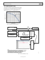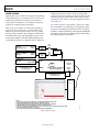
1
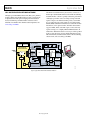
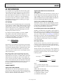
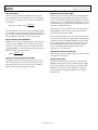
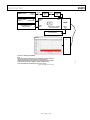
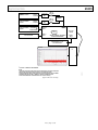
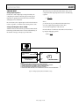
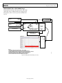
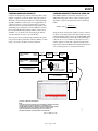
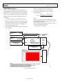
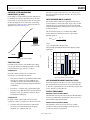
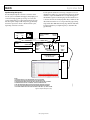
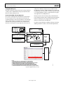
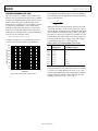
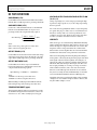
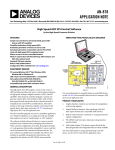
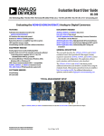
AN-835
APPLICATION NOTE
One Technology Way • P.O. Box 9106 • Norwood, MA 02062-9106, U.S.A. • Tel: 781.329.4700 • Fax: 781.461.3113 • www.analog.com
Understanding High Speed ADC Testing and Evaluation
by Alex Arrants, Brad Brannon and Rob Reeder
SCOPE
DYNAMIC TEST HARDWARE SETUP
This document describes both the characterization and production
test methods used by the High Speed Converter Group of Analog
Devices, Inc., to evaluate high speed analog-to-digital converters
(ADCs). While this application note should be considered a
reference, it is not a substitute for a product data sheet.
SNR, SINAD, worst spur, and IMD are tested using a hardware
setup similar to that shown in Figure 1. In production tests, the
test hardware is highly integrated, but the hardware principles
are the same. The basic setup for dynamic testing includes a
signal generator, band-pass filter, test fixture, low noise power
supplies, encode source (often integrated on the evaluation
board), data acquisition module, and data analysis software.
Analog Devices provides application hardware and software
to aid in bench evaluation.
WALL OUTLET
100V TO 240V AC
47Hz TO 63Hz
SWITCHING
POWER
SUPPLY
SWITCHING
POWER
SUPPLY
6V DC
2A MAX
SIGNAL
SYNTHESIZER
6V DC
2A MAX
4LO INPUT
ANALOG INPUT
SIGNAL
SYNTHESIZER
PC
RUNNING ADC
ANALYZER
OR VISUAL ANALOG
USER SOFTWARE
AGILENT
POWER SUPPLY
OPTIONAL
CLOCK
INPUT
SPECTRUM
ANALYZER
OSCILLOSCOPE
OR
SIGNAL
SYNTHESIZER
05941-001
GAIN CONTROL
INPUT
CW I/Q
OUTPUTS
Figure 1. Typical Characterization Test Setup
Rev. A | Page 1 of 28
AN-835
Application Note
TABLE OF CONTENTS
Scope .................................................................................................. 1
Dither Testing ............................................................................. 16
Dynamic Test Hardware Setup ....................................................... 1
Analog Input ............................................................................... 17
Revision History ............................................................................... 3
Analog Input Impedance ...................................................... 17
HSC-ADC-EVALC Evaluation Platform .................................. 4
Voltage Standing Wave Ratio (VSWR)................................ 17
Background ....................................................................................... 5
Analog Input Full-Scale Range (V p-p) .................................. 18
ADIsimADC ................................................................................. 5
Common-Mode Input Range (V) ............................................ 19
Analog Signal Source ................................................................... 6
Common-Mode Rejection Ratio (CMRR, dB) ...................... 19
Analog Signal Filter ...................................................................... 6
Aperture Delay (AD, ps)............................................................ 20
Encode Signal Sources ................................................................. 7
Aperture Jitter or Aperture Uncertainty (ps RMS) ................ 21
Power Supplies .............................................................................. 8
Crosstalk (dB) ............................................................................. 21
Data Acquisition ........................................................................... 8
Condition One ........................................................................ 21
AC Test Definitions .......................................................................... 9
Condition Two........................................................................ 21
FFT Testing.................................................................................... 9
Input-Referred Noise (LSB RMS) ............................................ 21
Single-Tone FFT ........................................................................... 9
Out-of-Range Recovery Time (CLK Cycles) ............................. 21
Signal-to-Noise Ratio (SNR, dB)............................................ 9
Digital Time Domain ................................................................. 21
Signal-to-Noise Ratio Referenced to Full Scale (SNRFS,
dBFS) .......................................................................................... 9
Minimum Conversion Rate (MSPS).................................... 21
Signal-to-Noise-and-Distortion (SINAD, dB) ..................... 9
Pipeline Delay (CLK Cycles) ................................................ 22
User-Defined Signal-to-Noise Ratio (UDSNR, dB) ............ 9
Propagation Delay (ns) .......................................................... 23
Noise Figure (NF, dB) .............................................................. 9
Encode Pulse Width or Encode Duty Cycle ....................... 23
Noise Floor (dBFS)................................................................. 10
Conversion Error Rate (CER)................................................... 24
Effective Number of Bits (ENOB, Bits) ............................... 10
DC Test Definitions ....................................................................... 25
Spurious-Free Dynamic Range (SFDR, dBc) ..................... 10
Gain Error (%FS)........................................................................ 25
Harmonic Distortion (dBc or dBFS) ................................... 10
Gain Matching (%FS) ................................................................ 25
Total Harmonic Distortion (THD, dBc) ............................. 10
Offset Error (%FS) ..................................................................... 25
Harmonic Image (dBc) .......................................................... 10
Offset Matching (mV) ............................................................... 25
Two-Tone FFT ............................................................................ 12
Temperature Drift (ppm) .......................................................... 25
F1 + F2 (dBc) .......................................................................... 12
Voltage Output High/Voltage Output Low (VOH/VOL, V) ..... 25
F2 − F1 (dBc) .......................................................................... 12
Linearity....................................................................................... 25
Second-Order Input Intercept Point (IIP2, dBm).............. 12
Differential Nonlinearity Error (DNL, LSB) ...................... 26
2F1 ± F2 and 2F2 ± F1 (dBc) ................................................ 12
Missing Code .......................................................................... 26
Third-Order Input Intercept Point (IIP3, dBm) ................ 12
Integral Nonlinearity Error (INL, LSB)............................... 26
Worst Other Spur (WoSpur, dBc) ........................................ 12
Power Supply Rejection Ratio (PSRR, dB) ............................. 27
Two-Tone SFDR (dBc) .......................................................... 12
References ........................................................................................ 28
Noise Power Ratio (NPR, dB) ................................................... 14
Additional References ................................................................ 28
Maximum Conversion Rate (MSPS) ................................... 21
Full Power Bandwidth (MHz) .................................................. 15
Rev. A | Page 2 of 28
Application Note
AN-835
REVISION HISTORY
6/10—Rev. 0 to Rev. A
Added Alex Arrants to by ................................................................ 1
Changes to Dynamic Test Hardware Setup Section and
Figure 1 ............................................................................................... 1
Changes to HSC-ADC-EVALC Evaluation Platform Section
and Figure 2........................................................................................ 4
Changes to Figure 3, ADIsimADC Section, and Figure 4 ........... 5
Changes to Analog Signal Source Section, Analog Signal Filter
Section, Figure 5, and Figure 6 ........................................................ 6
Changes to Encode Signal Sources Section ................................... 7
Changes to Figure 10, Power Supplies Section, Figure 11, and
Data Acquisition Section .................................................................. 8
Added Figure 12; Renumbered Sequentially ................................. 8
Changes to User-Defined Signal-to-Noise Ratio (UDSNR, dB)
Section and Noise Figure (NF, dB) Section ................................... 9
Changes to Noise Floor (dBFS) Section and Effective Number
of Bits (ENOB, Bits) Section .......................................................... 10
Changes to Figure 13 ...................................................................... 11
Changes to Figure 14 ...................................................................... 13
Changes to Figure 17 ...................................................................... 14
Changes to Figure 19 ...................................................................... 15
Changes to Dither Testing and Figure 20 .................................... 16
Changes to Figure 21 ...................................................................... 17
Changes to Figure 22 ...................................................................... 18
Changes to Common-Mode Input Range (V) Section, CommonMode Rejection Ratio (CMRR, dB) Section, and Figure 23 .......... 19
Changes to Aperture Delay (AD, ps) Section and Figure 24 ..... 20
Changes to Input-Referred Noise (LSB RMS) Section............... 21
Added Figure 26 .............................................................................. 21
Changes to Pipeline Delay (CLK Cycles) Section ....................... 22
Added Figure 27 .............................................................................. 22
Changes to Figure 28 ...................................................................... 23
Changes to Conversion Error Rate (CES) Section and
Table 1 ............................................................................................... 24
Added Figure 29 .............................................................................. 24
Changes to References Section ...................................................... 28
4/06—Revision 0: Initial Version
Rev. A | Page 3 of 28
AN-835
Application Note
HSC-ADC-EVALC EVALUATION PLATFORM
The FPGA-based buffer memory board can be connected to a
PC through a standard USB cable and used with the VisualAnalog
and SPIController software to quickly evaluate the performance
of the high speed ADCs. Users can change settings in the SPI
registers unique to the individual ADC product, view an FFT
for a specific analog input and sample rate, and analyze SNR,
SINAD, SFDR, and harmonic information, as well as time domain
information, such as gain and offset. The HSC-ADC-EVALC
supports CMOS, LVDS, and CML outputs. Some boards may
require an interposer or slightly different FIFO alternative. If
additional or different hardware is necessary, it will be specified
in the product data sheet. For more detailed information on the
HSC-ADC-EVALC, the SPIController, and how the VisualAnalog
software works, visit www.analog.com/FIFO.
The high speed ADC FIFO evaluation kit (HSC_ADC_EVALC)
includes a FPGA-based buffer memory board to capture blocks
of digital data from Analog Devices high speed ADC evaluation
boards, VisualAnalog®, and SPIController software. For more
information on the HSC-ADC-EVALC evaluation platform, visit
www.analog.com/FIFO.
ON-BOARD
VOLTAGE
REGULATORS
HSC-ADC-EVALC
SINGLE OR MULTICHANNEL
HIGH SPEED ADC
EVALUATION BOARD
n
J3*
LOGIC
FILTERED
ANALOG
INPUT
ADC
FPGA
CONFIGURATION
MODE
LED2
J2*
FIFO
CONTROL(9)
CLKA(2)
DATA BUS 1(18)
EXT SYNC2
J1*
UPLOAD
FPGA
DONE
J6
USB
CONTROLLER
USB
CONFIG
PROM
FPGA
CONFIG
PROM
FPGA GPIO(8)
SPI(7)
USB DIRECT(5)
CAPTURE
PORTB
PORTD
PORTC
PORTE
PORTA
CLKB(2)
EXT SYNC1
CLOCK
CIRCUIT
LED1
DATA(16)
DATA BUS 2(18)
FPGA
n
SPI
USB
USB
CONNECTOR
STANDARD
USB 2.0
ONBOARD
VOLTAGE
J4
REGULATORS
POWER
CONNECTOR
RECONFIG
J10
*DATA CONVERTER I/O CONNECTORS
JTAG
CONNECTOR
CLOCK INPUT
Figure 2. Typical HSC-ADC-EVALC Evaluation Platform
Rev. A | Page 4 of 28
05941-002
POWER
CONNECTOR
Application Note
AN-835
BACKGROUND
GENERAL PURPOSE I/O,
USB/SPI CONTROL
DATA BUS 1
DATA BUS 2
FPGA LOAD
SELECT
XILINX
VIRTEX-4
FPGA
DEBUG
PINS
ON BOARD
POWER SUPPLY
100MHz
OSCILLATOR
EXTERNAL
SYNC I/O
FPGA I/O
VOLTAGE MODE
CYPRESS USB
CONTROLLER
USB CONNECTOR
FPGA JTAG
CONNECTOR
5VDC POWER
INPUT
05941-003
FPGA CONFIG
PROM
Figure 3. HSC-ADC-EVALC: FPGA-Based Data Capture Board
ADIsimADC™ is Analog Devices ADC behavioral modeling tool.
ADIsimADC accurately models many of the time and frequency
domain errors common to ADCs. This tool can be invaluable in
terms of both simple converter selection and complete system
simulation. Although the tool is fully integrated into the
VisualAnalog software to aid in simple converter selection;
it is also supported by several third-party CAD vendors.
Currently, ADIsimADC is supported by MATLAB®, C++,
National Instruments LabVIEW™ SignalExpress, Agilent’s ADS,
and Applied Wave Research’s Visual System Stimulatior™. Others
will be available in the future. The tool can be downloaded from
the website along with a complete collection of current models.
Links are provided to third-party tools that support ADIsimADC.
For more information on ADIsimADC behavioral modeling, visit
www.analog.com/ADIsimADC. For more detailed information on
ADIsimADC, see the AN-737 Application Note at www.analog.com.
05941-004
ADIsimADC
Figure 4. VisualAnalog: Typical Canvas Showing an FFT and Time Domain
Performance Plots
Rev. A | Page 5 of 28
AN-835
Application Note
0
ANALOG SIGNAL SOURCE
IL 0.3dB @ 10MHz
–10
ATTENUATION (dB)
–20
–30
–40
–50
–60
40
ANALOG SIGNAL FILTER
60
80
100
120
FREQUENCY (MHz)
There are two types of filters that are often used for ADC testing:
low-pass filters and band-pass filters. These can be used
individually or combined to yield the level of performance
required for an application.
Figure 5. Typical Performance of TTE’s J97
0
–10
ATTENUATION (dB)
Both fixed frequency and tunable frequency band-pass filters
are used for device testing. The fixed frequency filters are typically
smaller than tunable filters and often provide slightly better
performance. Tunable filters allow testing across a wide range
of frequencies using one filter. Several filter manufacturers, including
K&L Microwave, TTE, and Allen Avionics, Inc., provide excellent
filters for ADC testing.
05941-005
Usually, dynamic testing employs a Rohde & Schwarz SMA/
SMHU/SMG/SMGU, an Agilent 8644 signal generator, a Wenzel
crystal oscillators or a Valpey Fisher crystal oscillator. These
sources have proven to provide exceptional performance (low
phase noise, flat frequency response, and reasonable harmonic
performance) for frequencies of a few kilohertz to those of a few
gigahertz. Harmonic performance of these generators is typically
not as good as the intrinsic linearity of a given ADC, mandating
the need for additional filtering between the signal generator
and the analog input to the ADC.
IL 3dB @ 100MHz
–20
–30
–40
Band-pass filters are used when analog frequencies are fixed
and will not be changed. Band-pass filters also eliminate much
of the wideband noise generated by signal sources and typically
provide the best performance for ADC testing. Filters such as
TTE’s Q70T series have a bandwidth defined as a percentage of
the center frequency. The more narrow the bandwidth, the less
noise that passes through the filter; however, the analog frequency
is more restricted, and there is a greater insertion loss. When a
center frequency is chosen, the bandwidth can be determined.
Ideally, a bandwidth of 5% to 6% should be selected, keeping in
mind that good noise performance is being traded for analog
frequency flexibility. As with low-pass filters, the band-pass filter
has a transition band that defines the shape between the 3 dB
frequency (above and below the center frequency) and the
frequency of the guaranteed stop-band performance. In the
case of TTE’s Q70T, the stop-band rejection is 60 dB.
–60
85
90
95
100
105
110
FREQUENCY (MHz)
115
08941-006
–50
Low-pass filters are a good choice when a wide range of analog
frequencies must be applied to the ADC. However, they allow
noise to pass from the signal generator to the ADC. This noise
may reduce the level of performance measured for the ADC. A
typical low-pass filter is the J97 available from TTE. Usually, lowpass filters have a transition band that defines where the pass
band ends and the stop band begins. Along with this specification,
a guaranteed stop-band rejection is specified. In the case of the
J97, the transition band is defined to be between 1.0 times and
1.2 times the 3 dB frequency, and the guaranteed stop-band
rejection is 80 dB. Energy beyond 1.2 times the 3 dB frequency
is reduced by a minimum of 80 dB.
Figure 6. Typical Band-Pass Performance of TTE’s Q70T
As noted previously, band-pass filters may only have a stop-band
rejection of 60 dB, meaning that signals that fall into the stop
band will be rejected by 60 dB. If, for example, a signal source
has a harmonic that is 25 dB below the fundamental, the effective
level of the harmonic is −85 dBc after a Q70T filter. For many
high performance ADCs, this is not sufficient. When performance
of −100 dBc or better is required, it is common to cascade a
band-pass filter with a low-pass filter. When selecting a low-pass
filter to follow a band-pass filter, the low-pass frequency should be
selected such that stop-band performance of the low-pass filter
optimally filters any harmonics that pass through the band-pass
filter. With a J97 low-pass filter, stop-band rejection is reached at
1.2 times the 3 dB frequency. If the second harmonic of the bandpass filter is set equal to 1.4 times the low-pass 3 dB frequency, it
ensures that all harmonics passing through the band-pass filter are
filtered and that the additional insertion loss of the low-pass filter
does not significantly reduce the level of the desired pass band. In
this case, the low-pass frequency should equal 1.4 times the bandpass frequency, and theoretically, the cascaded rejection should
be about 140 dB. Although this is difficult to achieve in practice
due to coupling and radiation effects, this technique is a useful
one and can achieve well beyond −100 dBc harmonic rejection.
Rev. A | Page 6 of 28
Application Note
AN-835
It is also worth noting that a 0.5 dB to 3 dB attenuator can be placed
between the band-pass and low-pass series combination. This helps
to provide a better match between the two filters, which are
nominally specified at 50 Ω.
When specifying filters, request those made with large cores to
prevent saturation. Filters are typically designed for an input power of
about +15 dBm. In many cases, however, ADC drive requirements
are much larger than this, causing core saturation and distortion.
Specifying larger cores reduces the spurious distortion caused
by core saturation. Finally, it is worth mentioning that filter
connectors can also be specified. Although adapters are easily
found to convert between connector types, using them introduces
mismatches that can subtly affect converter performance. While
this may not be a problem with 8-bit and 10-bit converters, it is
quite noticeable with 12-, 14-, and 16-bit converters.
It is very important that an appropriate clock oscillator be used in
each ADC design. Selection of the proper clock is aided by Analog
Devices AN-501 Application Note, AN-756 Application Note, and
Analog-to-Digital Converter Clock Optimization: A Test
Engineering Perspective and can be found at www.analog.com.
These application notes explain how to measure aperture jitter
and how to specify a clock that meets the required phase noise or
jitter specification. Failure to properly specify a clock source will
degrade SNR performance, as shown in Figure 8 and Figure 9.
As a reference, a typical Wenzel clock oscillator has about 0.07 ps
of aperture jitter, whereas the CMOS clock oscillators have about
0.3 ps or more of aperture jitter.
ENCODE SIGNAL SOURCES
05941-008
For high performance converters, stock signal generators usually
are insufficient as encode sources because of both close-in and
wideband phase noise. Fixed-frequency oscillators are typically
used for encode sources. High performance crystal oscillators
manufactured by Wenzel and Techtrol Cyclonetics, Inc., (TCI)
can be used. Wenzel’s Sprinter and Ultra Low Noise series can
offer optimum phase noise performance. Another source of
high quality encode sources is Valpey Fisher, which offers several
options, including differential PECLs and voltage-controlled
crystal oscillators (VCXOs). For less demanding applications,
standard CMOS clock modules can be used and are available
from various manufacturers. For end applications that require
the clock to be synchronized with an external reference, a VCXO in
a PLL loop can be employed as found in products like the AD9516.
05941-009
Figure 8. AD9445 with Analog IF of 130 MHz @ −1.0 dBFS using a
Wenzel Clock, SNR = 75.2 dBFS
05941-007
Figure 9. AD9445 with Analog IF of 130 MHz @ −1.0 dBFS using a
CMOS Clock, SNR = 71.2 dBFS
Figure 7. Typical Low Cost CMOS Clock Oscillator
When clock sources are not available with the desired jitter
performance, it is possible to divide a higher frequency clock
into lower rates. This has the effect of reducing the jitter at the
rate of 10 log(x), where x is the division ratio. The limitation of
this, however, is the jitter of the gates themselves. The AN-501
Application Note provides an indication of the clock jitter
associated with various logic families (see www.analog.com).
Rev. A | Page 7 of 28
AN-835
Application Note
REF2
ADP1706ARDZ-1.8-R7
U700
PWR_IN3
1
7
3
8
DIVIDER
AND MUXs
C708
4.7µF
DIV/Φ
LVPECL
DIV/Φ
LVPECL
DIV/Φ
DIV/Φ
DIV/Φ
SERIAL CONTROL PORT
AND
DIGITAL LOGIC
ΔT
ΔT
ΔT
ΔT
LVDS/CMOS
LVDS/CMOS
OUT0
OUT1
OUT2
OUT3
OUT4
OUT5
OUT6
OUT7
OUT8
OUT9
C711
0.01µF
EN
E704
SENSE
IN
IN2
OUT
OUT2
SS
2
PAD
5
1
2
DUT_AVDD1
6
450Ω
C715
4.7µF
Figure 12. ADP1706/ADP1707/ ADP1708Typical Application
DATA ACQUISITION
AD9516-0
05941-010
DIV/Φ
VOUT
1µF
GND
VCO
LVPECL
10µH
OUT
Figure 11. ADP3338/ADP3339Typical Application
STATUS
MONITOR
DIV/Φ
OUT
1µF
4
CLK
ADP3338/
ADP3339
IN
05941-031
REFIN
VIN
LF
PLL
REF1
SWITCHOVER
AND MONITOR
CP
For more information on designing power supplies for high
speed ADCs, see the CN0135 Circuit Note and the CN0137
Circuit Note at www.analog.com.
05941-011
When custom clocking is desired, a PLL is often required. A
PLL allows the ADC to be synchronized to an external clock
reference using a VCO or VCXO. However, it is difficult to clock
more than one device using a simple PLL, but adding delays
between the devices can facilitate such clocking. Devices such
as the AD9516 are ideal for clock cleanup and distribution as
shown in Figure 10. The additive jitter of the AD9516 is about
0.22 ps, and the device is optimized for driving ADCs, DACs,
and various logic devices.
Figure 10. AD9516 Low Jitter Clock Source
POWER SUPPLIES
Power supplies for ADCs are very important. Therefore, it is
important to provide clean, quiet power supplies because most
ADCs can modulate excessive noise on these input bias pins. To
fully understand how an ADC performs with a certain amount
of noise on these pins, the power supply rejection ratios of all
the supplies should be measured and understood over the
frequency band of interest. While switching regulators are fine
for many applications, some examples include the ADP5020,
ADP2108, and the ADP2114. However, linear regulators often
provide a quieter, higher performance solution. Devices such as the
ADP3338/ADP3339 (see Figure 11) and ADP1706/ADP1707/
ADP1708 (see Figure 12) series provide very low noise and
well-regulated sources, and they are suitable for most ADC
applications. Additionally, they are available in a variety of
voltages and can source up to 1 A.
Data acquisition and processing is accomplished with high speed
caching memory. Data is collected at full ADC speed or can be
decimated depending on the testing method used. Bench testing
uses the HSC-ADC-EVALC evaluation platform (no decimation
required) in conjunction with the VisualAnalog software (see
the HSC-ADC-EVALC Evaluation Platform section for more
details). Typically 16k, 32k, or 64k FFTs are performed, but
bench FFTs can be as large as 4M samples. When the analog
input source is not synchronized with the clock (noncoherent
sampling), a Hanning or Blackman-Harris windowing function
is typically used. (For more information, see “On the Use of
Windows for Harmonic Analysis with the Discrete Fourier
Transform,” fredric j. harris, Proceedings on the IEEE. Vol. 66,
No. 1, January 1978.)
Rev. A | Page 8 of 28
Application Note
AN-835
AC TEST DEFINITIONS
AC or dynamic tests are typically made with the analog signal
at the rated frequency with a signal power of 0.1 dB, 0.5 dB, or
1 dB below full scale (dBFS). If different amplitudes are used,
they will be defined in the data sheet test conditions. For these
tests, the encode rate is usually set at or near the maximum
rated value. The data sheet should be consulted to determine
the remainder of the test conditions, including power supply
and temperature conditions.
Signal-to-Noise Ratio Referenced to Full Scale
(SNRFS, dBFS)
FFT TESTING
The SINAD is the ratio of the rms signal amplitude to the rms
value of the sum of all spectral components, including harmonics
but excluding dc. The difference between SNR and SINAD is
the energy contained in the first six harmonics.
Both coherent and noncoherent FFT testing can be used, depending
on the actual test conditions. When coherent testing is used, the
analog frequency is chosen such that the captured data samples
exercise as many converter codes as possible in the record length.
This is accomplished by using a prime relationship between the
analog frequency and the encode rate.
For example, if coherent sampling is used and a 10 MHz
analog input is desired with a specified sample rate of
65 MSPS, the calculated coherent analog input frequency
is 10.0015258789063 MHz, or exactly 2521 cycles. This can
be calculated using the following equation:
Cycles =
f DESIRED _ FREQUENCY
Sample _ Rate
FFT _ Samples
The SNRFS is the ratio of the rms full scale to the rms value of
the sum of all spectral components except the first six harmonics
and dc. SNRFS is expressed in decibels referenced to full scale
(dBFS). The difference between SNR and SNRFS is the difference
between the fundamental amplitude and full scale.
Signal-to-Noise-and-Distortion (SINAD, dB)
User-Defined Signal-to-Noise Ratio (UDSNR, dB)
UDSNR is a term that refers to the ability to set the integration
limits of the noise over a user-definable span of frequencies. See
the AN-905 Application Note, VisualAnalog™ Converter Evaluation
Tool Version 1.0 User Manual, at www.analog.com for details on
FFT analysis. It is the ratio of the rms signal amplitude to the rms
sum of all spectral components except the first six harmonics
and dc within the specified band set by the user. UDSNR is
reported in decibels.
Noise Figure (NF, dB)
The number of cycles should be rounded to the nearest integer.
When possible, the nearest prime number should be selected to
ensure that the maximum number of quantization levels of the
converter is exercised. When the number of cycles has been
selected, the previous equation can be solved using the desired
analog input frequency.
FFT testing typically results in measurements expressed in
decibels. Units can be expressed in dBc, which is the desired
signal referenced to the carrier, or in dBFS, which is the desired
signal referenced to the full scale of the converter. Either unit
can be converted to the other by adding or subtracting the level
of the carrier from full scale. (For more information about FFT
testing, see “The FFT: Fundamentals and Concepts,” Tektronix,
Inc., 070-1754-00, Production Group 45, first printing
December 1975.)
SINGLE-TONE FFT
Signal-to-Noise Ratio (SNR, dB)
The SNR is the ratio of the rms signal amplitude to the rms
value of the sum of all spectral components except the first six
harmonics and dc. As the input level is decreased, SNR typically
decreases decibel-for-decibel in a linear fashion.
The NF is the ratio of the noise power at the output of a device
to the noise power at the input to the device, where the input
noise temperature is equal to the reference temperature (298 K).
The noise figure is expressed in decibels.
The NF of an ADC can be computed for a single configuration.
Assuming that the input range, termination, and sample rate are
fixed, the noise figure for an ADC can be calculated using the
following equation:
⎛ V 2rms / Z IN
10 × log ⎜⎜
Noise Figure =
⎝ 0.001
⎞
⎟⎟ − SNRFS −
⎠
⎛ Encode Frequency ⎞
⎛ k ×T × B ⎞
10 × log ⎜
⎟ − 10 × log ⎜
⎟
2
⎝ 0.001 ⎠
⎝
⎠
where:
V rms = rms full-scale input voltage.
ZIN = ADC input impedance or input network and ADC input
impedance.
SNRFS = full-scale ADC SNR.
Encode Frequency = ADC clock rate.
k = Boltzman’s constant = 1.38 × 10⁻²³.
T = temperature in Kelvin = 298 K.
B = bandwidth of interest (Hz).
Rev. A | Page 9 of 28
AN-835
Application Note
Noise Floor (dBFS)
Harmonic Distortion (dBc or dBFS)
Noise floor is a term used in VisualAnalog software (see the
AN-905 Application Note, VisualAnalog™ Converter Evaluation
Tool Version 1.0 User Manual, at www.analog.com). Noise floor
is equivalent to
A harmonic is a spectral component that is an integer multiple
of the driven analog input frequency. For example, the frequency
of the second harmonic is twice the analog input. Most ADCs have
specifications for one or more harmonics. Typically, the second
and third harmonics are singled out because they have the worst
performance of all the harmonics.
⎛ FFT Bins ⎞
Noise Floor = SNRFS − 10 log ⎜
⎟
2
⎠
⎝
This is an indication of the average noise in each FFT bin. If the
size of the FFT is doubled, this number decreases by 3 dB. Noise
floor does not provide an absolute measurement but instead gives a
relative indication of where the noise is for a given setup.
Effective Number of Bits (ENOB, Bits)
ENOB provides a measure of the performance of the ADC that
is expressed in bits. ENOB is most accurately measured using
a sine wave, curve-fit method. The most common method for
computing ENOB is to use the following equation based on the
SINAD at the full scale of the converter:
ENOB =
SINAD − 1.76
6.02
Harmonic distortion, no matter the order, is the ratio of the rms
signal amplitude to the rms value of the specified harmonic
component, reported in dBc or dBFS.
Because ADCs are nonlinear devices, the output is rich in spectral
components. The worst spurious energy may not be directly related
to the first two harmonics (2HD and 3HD) and is measured by
the worst other spurious (WoSpur). WoSpur is the ratio of the
rms signal amplitude to the rms value of the worst spurious
component excluding the first six harmonically related
components; it is reported in dBc.
Total Harmonic Distortion (THD, dBc)
THD is the ratio of the rms signal energy to the rms value of the
sum of the first six harmonics.
Spurious-Free Dynamic Range (SFDR, dBc)
The SFDR is the ratio of the rms value of the signal to the rms
value of the peak spurious spectral component for the analog
input that produces the worst result. In most cases, SFDR is a
harmonic of the input signal applied to the ADC.
Harmonic Image (dBc)
The harmonic image measurement result is valid only when
analyzing interleaved ADCs. This specification does not apply
to most ADCs. Harmonic image is the ratio of the rms signal
amplitude to the rms value of the nonharmonic component
generated from the clocking phase difference of two ADCs,
reported in dBc.
Rev. A | Page 10 of 28
Application Note
WENZEL XTAL
ROHDE & SCHWARZ
AGILENT
WENZEL XTAL
ROHDE & SCHWARZ
AGILENT
AN-835
1dB PAD1
ANALOG
OUTPUT
DIFFERENTIAL
OR
SINGLE-ENDED
TTE OR K&L
MICROWAVE
BPF
1dB PAD1
TTE OR K&L
MICROWAVE
LPF1
ANALOG
INPUT
ENCODE
INPUT
ADC
DUT
SUPPLY
INPUT
STANDARDIZED 6V TO 9V
OR LAB SUPPLIES
AD92xx, AD94xx, OR AD66xx
EVALUATION BOARD
ADC-FIFO
BOARD
SUPPLY
INPUT
STANDARDIZED 6V TO 9V
OR LAB SUPPLIES
MONITOR
PC
USB
TO IMPROVE PERFORMANCE.
NOTES
1. AIN LEVELS SHOULD BE ADJUSTED FOR THE FREQUENCY AND LEVEL SPECIFIED.
2. ENCODE SETTING SHOULD BE ADJUSTED TO THE SPECIFIED RATE.
3. UNLESS ONBOARD REGULATORS ARE USED, SUPPLIES SHOULD BE AT NOMINAL.
4. TEMPERATURE SHOULD BE AT AMBIENT, UNLESS OTHERWISE NOTED.
5. USE THE APPROPRIATE CONFIGURATION FILE FOR VisualAnalog.
Figure 13. Single-Tone Test Setup
Rev. A | Page 11 of 28
05941-012
1 OPTIONAL
AN-835
Application Note
TWO-TONE FFT
2F1 ± F2 and 2F2 ± F1 (dBc)
When multiple tones are passed through a converter with
nonlinearities, intermodulation distortion products (IMD)
result. Two-tone testing in an ADC is a means of specifying
these nonlinearities. Because many of the distortion products
may be relatively high in the analog spectrum, it is possible that
the frequencies have aliased. This should be kept in mind when
identifying distortion products.
These terms represent the third-order distortion products of the
converter. The measure of each term is the ratio of its rms value
to the rms value of one of the two input tones expressed in dBc.
The peak spurious component is considered an IMD product.
F1 + F2 (dBc)
This term represents the second-order distortion product that
appears at the frequency and is the sum of the two input frequencies. The measure of this term is the ratio of its rms value
to the rms value of one of the two input tones expressed in dBc.
F2 − F1 (dBc)
This term represents the second-order distortion product that
appears at the frequency and is the difference of the two input
frequencies. The measure of this term is the ratio of its rms value
to the rms value of one of the two input tones expressed in dBc.
Second-Order Input Intercept Point (IIP2, dBm)
The IIP2 is the measure of the full-scale input signal power
of the converter minus the IMD second-order products. It is
reported in dBm.
Third-Order Input Intercept Point (IIP3, dBm)
The IIP3 is the measure of the full-scale input signal power of
the converter minus half the IMD third-order products. It is
reported in dBm.
Worst Other Spur (WoSpur, dBc)
WoSpur is the worst resulting spurious not related to the secondor third-order distortion products resulting from mixing two
analog input signals. The measure of this term is the ratio of
its rms value to the rms value of one of the two input tones
expressed in dBc.
Two-Tone SFDR (dBc)
The SFDR is the ratio of the rms value of the signal to the rms
value of the peak spurious spectral component for the analog
input that produces the worst result. In most cases, SFDR is a
harmonic of the input signal applied to the ADC.
Rev. A | Page 12 of 28
Application Note
WENZEL XTAL
ROHDE & SCHWARZ
AGILENT
AN-835
TTE OR K&L
MICROWAVE
BPF
ANALOG
OUTPUT
1dB TO
10dB PAD1
COMBINER
WENZEL XTAL
ROHDE & SCHWARZ
AGILENT
WENZEL XTAL
ROHDE & SCHWARZ
AGILENT
TTE OR K&L
MICROWAVE
BPF
ANALOG
OUTPUT
DIFFERENTIAL
OR
SINGLE-ENDED
1dB TO
10dB PAD1
ANALOG
INPUT
ENCODE
INPUT
ADC
DUT
SUPPLY
INPUT
STANDARDIZED 6V TO 9V
OR LAB SUPPLIES
AD92xx, AD94xx, OR AD66xx
EVALUATION BOARD
ADC-FIFO
BOARD
SUPPLY
INPUT
STANDARDIZED 6V TO 9V
OR LAB SUPPLIES
MONITOR
PC
USB
TO IMPROVE PERFORMANCE.
NOTES
1. AIN LEVELS SHOULD BE ADJUSTED FOR THE FREQUENCY AND LEVEL SPECIFIED.
2. ENCODE SETTING SHOULD BE ADJUSTED TO THE SPECIFIED RATE.
3. UNLESS ONBOARD REGULATORS ARE USED, SUPPLIES SHOULD BE AT NOMINAL.
4. TEMPERATURE SHOULD BE AT AMBIENT, UNLESS OTHERWISE NOTED.
5. USE THE APPROPRIATE CONFIGURATION FILE FOR VisualAnalog.
Figure 14. Two-Tone Test Setup
Rev. A | Page 13 of 28
05941-013
1 OPTIONAL
AN-835
Application Note
NOISE POWER RATIO (NPR, dB)
NPR is a dynamic test that is used to assess the performance of
converters with a fully loaded Gaussian noise source. The noise
level is adjusted such that the converter is loaded just below the
point of clipping with a Nyquist-limited noise source. Then a
narrow band of noise is removed with a deep notch filter. The
noise within the notch is measured using FFT techniques
to determine the ratio of noise density in the notch to the noise
density without the notch. The results are expressed in decibels. NPR
is optimized just prior to clipping, as shown in Figure 15. When
clipping begins, NPR falls off rapidly as the input signal is increased.
If the input signal is reduced, NPR falls off approximately 1 dB
for each decibel reduction in noise power.
86
0
–20
14-BIT
66
61
12-BIT
56
51
10-BIT
–60
–80
–100
41
–25
–40
–20
–15
–120
0
0
–10
05941-015
46
05941-014
5
WENZEL XTAL
ROHDE & SCHWARZ
AGILENT
ANALOG
OUTPUT
DIFFERENTIAL
OR
SINGLE-ENDED
18MHz
NOISE/COM
NOTCH FILTER
TTE OR
K&L MICROWAVE
ANTI-ALIAS FILTER
20
25
1dB
PAD
ANALOG
INPUT
ENCODE
INPUT
ADC
DUT
STANDARDIZED 6V TO 9V
OR LAB SUPPLIES
15
30
Figure 16. Typical NPR Response for a 12-Bit Converter
Figure 15. Typical NPR Curves
NOISE/COM
NC7108
NOISE GENERATOR
10
FREQUENCY (MHz)
20 log (VO/N rms) (dBFS)
SUPPLY
INPUT
AD92xx, AD94xx, OR AD66xx
EVALUATION BOARD
ADC-FIFO
BOARD
SUPPLY
INPUT
STANDARDIZED 6V TO 9V
OR LAB SUPPLIES
MONITOR
PC
USB
NOTES
1. SET NOISE/COM TO ~5dBm OR DECREMENT/INCREMENT FOR APPROPRIATE NOISE INPUT LEVEL.
2. ENCODE SETTING SHOULD BE ADJUSTED TO THE SPECIFIED RATE.
3. UNLESS ONBOARD REGULATORS ARE USED, SUPPLIES SHOULD BE AT NOMINAL.
4. TEMPERATURE SHOULD BE AT AMBIENT, UNLESS OTHERWISE NOTED.
5. USE THE APPROPRIATE CONFIGURATION FILE FOR VisualAnalog.
6. USE AN ADC-FIFO BOARD WITH AT LEAST 64k.
Figure 17. NPR Test Setup
Rev. A | Page 14 of 28
05941-016
NPR (dB)
71
AMPLITUDE (dBFS)
76
36
–30
NPR = 60.83dB
NOTCH = 18.0MHz
NOTCH WIDTH = 3.0MHz
16-BIT
81
Application Note
AN-835
FULL POWER BANDWIDTH (MHz)
Analog input bandwidth is the analog input frequency at which
the spectral power of the fundamental frequency (as determined
by the FFT analysis) is reduced by 3 dB. A particular value of
SFDR or SNR performance is not implied by this test.
0
–2
–3dB CUTOFF = 315MHz
–3
–4
–5
–6
–7
–8
05941-017
–9
–10
0
50
100
150
200
250
300
350
400
450
500
FREQUENCY (MHz)
Figure 18. Typical Full Power Bandwidth Response
ROHDE & SCHWARZ
AGILENT
TEE
ADAPTER
ANALOG
OUTPUT
ANALOG
BOONTON
INPUT
RF VOLTMETER
GPIB
WENZEL XTAL
ROHDE & SCHWARZ
AGILENT
DIFFERENTIAL
OR
SINGLE-ENDED
ANALOG
INPUT
ENCODE
INPUT
ADC
DUT
STANDARDIZED 6V TO 9V
OR LAB SUPPLIES
SUPPLY
INPUT
AD92xx, AD94xx, OR AD66xx
EVALUATION BOARD
ADC-FIFO
BOARD
SUPPLY
INPUT
STANDARDIZED 6V TO 9V
OR LAB SUPPLIES
MONITOR
PC
GPIB
USB
NOTES
1. AIN LEVELS SHOULD BE ADJUSTED FOR –1dB AT A 10MHz REFERENCE FREQUENCY.
2. ENCODE SETTING SHOULD BE ADJUSTED TO THE SPECIFIED RATE.
3. UNLESS ONBOARD REGULATORS ARE USED, SUPPLIES SHOULD BE AT NOMINAL.
4. TEMPERATURE SHOULD BE AT AMBIENT, UNLESS OTHERWISE NOTED.
5. USE THE APPROPRIATE CONFIGURATION FILE FOR VisualAnalog.
6. BOONTON PROBES SHOULD USE UNTERMINATED ADAPTERS.
Figure 19. Full Power Bandwidth Test Setup
Rev. A | Page 15 of 28
05941-018
FUNDAMENTAL LEVEL (dB)
–1
AN-835
Application Note
wideband analog noise is added to the input and the digital
equivalent is subtracted from the output. The net effect of either
technique is that spurious performance of the converter is greatly
enhanced. For more details, see the AN-410 Application Note at
www.analog.com.
DITHER TESTING
Applying extra noise to an ADC’s analog input causes dithering
of the transfer function, reducing the spurious caused by static
nonlinearities. While dither does little to reduce distortion
caused by slew rate limitations, it is very efficient at reducing
localized errors that hinder ADC performance.
It is common for spurious performance to improve by 15 dB or
more when dither is used, depending on the application. Many
data sheets include dithered performance plots for comparison.
In addition, using the VisualAnalog software with the ADIsimADC
allows dither to be added to the simulation, further demonstrating
how dither will improve performance.
There are two types of dither: out-of-band and wideband. As
shown in the setup in Figure 20, out-of-band dither is bandlimited noise placed out of band, where it does not spectrally
disrupt converter performance. This technique is commonly used
in communication systems, where digital filters are used to select
desired signals and filter out all others. Wideband dither is often
used in high performance test equipment. In this configuration,
NOISE/COM
DNG7500
NOISE GENERATOR
ANALOG
OUTPUT
TTE OR K&L
MICROWAVE
1.5MHz
1dB
PAD
COMBINER
WENZEL XTAL
ROHDE & SCHWARZ
AGILENT
WENZEL XTAL
ROHDE & SCHWARZ
AGILENT
ANALOG
OUTPUT
DIFFERENTIAL
OR
SINGLE-ENDED
TTE OR K&L
MICROWAVE
BPF
1dB
PAD
ANALOG
INPUT
ENCODE
INPUT
ADC
DUT
STANDARDIZED 6V TO 9V
OR LAB SUPPLIES
SUPPLY
INPUT
AD92xx, AD94xx, OR AD66xx
EVALUATION BOARD
ADC-FIFO
BOARD
SUPPLY
INPUT
STANDARDIZED 6V TO 9V
OR LAB SUPPLIES
MONITOR
PC
NOTES
1. AIN LEVELS SHOULD BE ADJUSTED FOR THE FREQUENCY AND LEVEL SPECIFIED.
2. ENCODE SETTING SHOULD BE ADJUSTED TO THE SPECIFIED RATE.
3. UNLESS ONBOARD REGULATORS ARE USED, SUPPLIES SHOULD BE AT NOMINAL.
4. TEMPERATURE SHOULD BE AT AMBIENT, UNLESS OTHERWISE NOTED.
5. USE THE APPROPRIATE CONFIGURATION FILE FOR VisualAnalog. ADJUST DC BINS TO EXCLUDE DITHER.
6. USE AN ADC-FIFO BOARD WITH AT LEAST 64k.
7. ADJUST NOISE/COM DITHER LEVEL FOR MAXIMUM SFDR PERFORMANCE.
Figure 20. Dither Test Setup
Rev. A | Page 16 of 28
05941-019
USB
Application Note
AN-835
ANALOG INPUT
The amount of power reflected back from the device can be
computed from the input impedance based on the following
equation:
Analog Input Impedance
It is the ratio of the complex input voltage divided by the
complex input current for the analog input. Analog input
impedance is typically measured with a network analyzer
and displayed on a Smith chart.
ρ=
Z IN − Z 0
Z IN + Z 0
where:
ρ is the amount of power reflected back from the device.
ZIN is the complex input impedance of the ADC.
Z0 is the desired impedance of the network.
In some instances, the complex input can be broken down into
resistive, capacitive, or inductive terms and reported as such.
Voltage Standing Wave Ratio (VSWR)
VSWR is a measure of the amount of power that is reflected back
from the input of the ADC. This is a measure of the efficiency of
the transfer of energy to the input port of the ADC.
From the reflection coefficient, the VSWR can be calculated
by using the following equation:
VSWR =
1+ ρ
1− ρ
ENA5071B
NETWORK ANALYZER
WENZEL XTAL
ROHDE & SCHWARZ
AGILENT
DIFFERENTIAL
OR
SINGLE-ENDED
ANALOG
INPUT
ENCODE
INPUT
ADC
DUT
SUPPLY
INPUT
AD92xx, AD94xx, OR AD66xx
EVALUATION BOARD
NOTES
1. ENCODE SETTING SHOULD BE ADJUSTED TO THE SPECIFIED RATE.
2. UNLESS ONBOARD REGULATORS ARE USED, SUPPLIES SHOULD BE AT NOMINAL.
3. TEMPERATURE SHOULD BE AT AMBIENT, UNLESS OTHERWISE NOTED.
4. USE THE APPROPRIATE CONFIGURATION FILE FOR VisualAnalog.
5. CALIBRATE NETWORK ANALYZER (3.5mm CALIBRATION KIT, PART NO. 85033C OR EQUIVALENT.
Figure 21. Analog Input Impedance and VSWR Test Setup
Rev. A | Page 17 of 28
05941-020
STANDARDIZED 6V TO 9V
OR LAB SUPPLIES
AN-835
Application Note
ANALOG INPUT FULL-SCALE RANGE (V p-p)
Analog input full-scale range is the range of peak-to-peak voltage
(either single-ended or differential) that can be applied to the
analog input(s) of the converter to generate a valid full-scale
response.
ROHDE & SCHWARZ
AGILENT
ANALOG
BOONTON
INPUT
RF VOLTMETER
ANALOG
OUTPUT
GPIB
WENZEL XTAL
ROHDE & SCHWARZ
AGILENT
DIFFERENTIAL
OR
SINGLE-ENDED
ANALOG
INPUT
ENCODE
INPUT
ADC
DUT
STANDARDIZED 6V TO 9V
OR LAB SUPPLIES
SUPPLY
INPUT
AD92xx, AD94xx, OR AD66xx
EVALUATION BOARD
ADC-FIFO
BOARD
SUPPLY
INPUT
STANDARDIZED 6V TO 9V
OR LAB SUPPLIES
MONITOR
PC
GPIB
NOTES
1. AIN LEVELS SHOULD BE ADJUSTED FOR –1dB AT 10MHz.
2. ENCODE SETTING SHOULD BE ADJUSTED TO THE SPECIFIED RATE.
3. UNLESS ONBOARD REGULATORS ARE USED, SUPPLIES SHOULD BE AT NOMINAL.
4. TEMPERATURE SHOULD BE AT AMBIENT, UNLESS OTHERWISE NOTED.
5. USE THE APPROPRIATE CONFIGURATION FILE FOR VisualAnalog.
6. BOONTON PROBES SHOULD USE UNTERMINATED ADAPTERS.
Figure 22. Analog Input Full-Scale Range Test Setup
Rev. A | Page 18 of 28
05941-021
USB
Application Note
AN-835
COMMON-MODE INPUT RANGE (V)
COMMON-MODE REJECTION RATIO (CMRR, dB)
Common-mode input range is the dc offset range that is either
applied or supplied to both of the ADC’s analog input pins for
which the converter will operate within its normal signal range.
Typically, unbuffered converters have to be supplied with a dc
common-mode bias to operate properly. This bias is usually
AVDD/2 and can be set with an external voltage divider or the
VCM/CML pin provided by the converter. Buffered converters
have an internal buffer and typically provide the common-mode
(AVDD/2 + 0.7 V) directly on the analog input pins without
any other hardware necessary to provide this bias.
The CMRR is defined as the amount of rejection on the
differential analog inputs when a common signal is applied.
Typically, it is expressed in decibels and can be calculated as
follows:
⎛ A
CMRR = 20 log ⎜ DIFFERENTIAL
⎜ ACOMMON MODE
⎝
Simply tie the two analog inputs together, provide a commonmode bias on the analog inputs if needed, and inject an input
signal near full-scale of the converter. To calculate CMRR, simple
record the fundamental spur level (dB) on the FFT display to
collect the ACOMMON MODE number. To collect the ADIFFERENTIAL
number, simply record the analog input level applied at the
inputs of the converter in dB. This measurement is then repeated
over several frequencies or over the band of interest.
Every converter has an optimum range in which it can operate
and provide excellent performance. It maybe a limited or a wide
range, to be certain consult the converter’s data sheet.
WENZEL XTAL
ROHDE & SCHWARZ
AGILENT
WENZEL XTAL
ROHDE & SCHWARZ
AGILENT
1dB PAD1
ANALOG
OUTPUT
DIFFERENTIAL
OR
SINGLE-ENDED
TTE OR K&L
MICROWAVE
BPF
ENCODE
INPUT
1dB PAD1
VCC
TTE OR K&L
MICROWAVE
LPF1
ANALOG
INPUT
ADC
DUT
SUPPLY
INPUT
STANDARDIZED 6V TO 9V
OR LAB SUPPLIES
⎞
⎟
⎟
⎠
AD92xx, AD94xx, OR AD66xx
EVALUATION BOARD
ADC-FIFO
BOARD
SUPPLY
INPUT
STANDARDIZED 6V TO 9V
OR LAB SUPPLIES
MONITOR
PC
USB
NOTES
1. AIN LEVELS SHOULD BE ADJUSTED FOR THE FREQUENCY AND LEVEL SPECIFIED.
2. ENCODE SETTING SHOULD BE ADJUSTED TO THE SPECIFIED RATE.
3. UNLESS ONBOARD REGULATORS ARE USED, SUPPLIES SHOULD BE AT NOMINAL.
4. TEMPERATURE SHOULD BE AT AMBIENT, UNLESS OTHERWISE NOTED.
5. USE THE APPROPRIATE CONFIGURATION FILE FOR VisualAnalog.
6. RESISTIVE DIVIDER MAY NOT BE NECESSARY FOR SOME ADCs.
Figure 23. CMRR Test Setup
Rev. A | Page 19 of 28
05941-022
1 OPTIONAL TO IMPROVE PERFORMANCE.
AN-835
Application Note
APERTURE DELAY (AD, ps)
AD is a measure of the difference in the delay between the
analog path and the encode path. It is measured by observing
the time from the 50% point of the rising edge of the sample
clock to the time at which the input signal is actually sampled.
5.
Remove the shorting bar from the analog input and
reconnect the analog input as shown in Figure 24.
6.
Record the new offset value and use it to solve the
following equation:
⎛ (Code AVERAGE − Offset )/(2 N / 2) ⎞
⎟
t AD = sin −1 ⎜
⎟
⎜
2π × Frequency
⎠
⎝
Aperture delay can be measured by using the following test
configuration:
1.
Connect the analog input to an analog filtered source.
2.
Using a program like VisualAnalog, adjust the input until
the single-tone FFT results in a full-scale signal (0 dBFS).
3.
Disconnect the analog input and use a shorting bar to
short the analog input to ground.
4.
Use a continuous average time domain plot to measure the
offset of the part.
WENZEL XTAL
ROHDE & SCHWARZ
AGILENT
where:
CodeAVERAGE is the new offset value obtained after removing
the shorting bar from the analog input and reconnecting
the analog input (see Step 5).
Offset is the offset of the part measured using a continuous
average time domain plot (see Step 4).
2N/2 is the midscale of an ADC.
ANALOG
OUTPUT
SHORTING
BAR
TEE
ADAPTER
WENZEL XTAL
ROHDE & SCHWARZ
AGILENT
DIFFERENTIAL
OR
SINGLE-ENDED
ANALOG
INPUT
ENCODE
INPUT
ADC
DUT
STANDARDIZED 6V TO 9V
OR LAB SUPPLIES
SUPPLY
INPUT
AD92xx, AD94xx, OR AD66xx
EVALUATION BOARD
ADC-FIFO
BOARD
SUPPLY
INPUT
STANDARDIZED 6V TO 9V
OR LAB SUPPLIES
MONITOR
PC
NOTES
1. AIN LEVELS SHOULD BE ADJUSTED FOR 0dBFS OUTPUT FOR THE INPUT FREQUENCY OF MIDBAND.
2. ENCODE SETTING SHOULD BE ADJUSTED TO THE SPECIFIED RATE.
3. UNLESS ONBOARD REGULATORS ARE USED, SUPPLIES SHOULD BE AT NOMINAL.
4. TEMPERATURE SHOULD BE AT AMBIENT, UNLESS OTHERWISE NOTED.
5. USE THE APPROPRIATE CONFIGURATION FILE FOR VisualAnalog.
Figure 24. Aperture Delay Test Setup
Rev. A | Page 20 of 28
05941-023
USB
Application Note
AN-835
APERTURE JITTER OR APERTURE
UNCERTAINTY (ps RMS)
It is the sample-to-sample variation in aperture delay that can
be manifested as frequency-dependent noise on the ADC
input. Details on measuring aperture jitter can be found in
the AN-501 Application Note, and details on converting
aperture jitter to phase noise can be found in the AN-756
Application Note at www.analog.com.
All results are expressed in decibels as a ratio of the energy of
the undesired signal on the quite channel to the energy on the
driven channel.
INPUT-REFERRED NOISE (LSB RMS)
It is a measure of the wideband noise generated by the ADC, as
shown in Figure 26. A histogram of the output codes is created
while the input is grounded. Input-referred noise is calculated
using the standard deviation of the histograms, and it is presented
in terms of LSB rms.
This measurement can also be correlated using SNRFS
measurements and converting decibels to volts using the
following equation:
NoiseINPUT =
dV
V p- p
2 × 2 × 10SNR / 20
where:
V p-p is the ADC full-scale input range.
SNR is the full-scale SNR performance when driven by a small
input signal.
ERROR VOLTAGE
1.2
1.006 LSB rms
Figure 25. Aperture Uncertainty
CROSSTALK (dB)
It is defined as the measure of any feedthrough coupling
onto the quiet channel of a multichannel ADC. Crosstalk
is measured in three ways under two conditions.
1.0
NUMBER OF HITS (Millions)
dt
05941-024
ENCODE
0.8
0.6
0.4
05941-026
0.2
Condition One
If a signal is driven near full scale, crosstalk can be
measured by one of the following methods:
•
•
Drive any two channels using a different midbaseband
frequency for each that are at least 2 MHz apart at
−0.5 dBFS. Record the same fundamental frequency
on any open channel (nondriven). Repeat for all channel
combinations.
Drive any N − 1 channel using a single midbaseband
frequency at −0.5 dBFS. Record the same fundamental
frequency on any open channel (nondriven). Repeat
for all channel combinations.
Condition Two
If a signal is driven 3 dB over full scale, known as the
overdriven condition, crosstalk can be measured as follows:
•
Use either method described in the Condition One
section; however, with a midbaseband frequency
amplitude set to 3 dB above full scale.
0
N–3
N–2
N–1
N
N+1
N+2
N+3
CODE
Figure 26. Input Referred Noise Histogram
OUT-OF-RANGE RECOVERY TIME (CLK CYCLES)
It is the time required for the ADC to recover to the rated accuracy
after an input transient moves from 10% above positive full scale
to 10% above negative full scale or from 10% below negative full
scale to 10% below positive full scale.
DIGITAL TIME DOMAIN
Minimum Conversion Rate (MSPS)
The minimum conversion rate is the clock rate at which the SNR of
the lowest specified analog signal frequency drops by no more
than 3 dB below the guaranteed limit.
Maximum Conversion Rate (MSPS)
The maximum conversion rate is the clock rate at which
parametric testing is performed. Higher operating rates are
possible, but they are not guaranteed.
Rev. A | Page 21 of 28
AN-835
Application Note
Pipeline Delay (CLK Cycles)
For the general evaluation board setup, see Figure 27. Use one
channel of an oscilloscope to capture the analog input. Use another
channel to capture the MSB data bit out. Setup the trigger for
this channel to capture on the rising edge. Use the vertical cursors
to measure the amount of delay. Pipeline delay is defined as the
delta time between the zero crossing of the analog input rising
edge and the 50% MSB data bit rising edge. Take the delta time
found and divide it by 1/sample frequency to determine the
pipeline delay.
It is the delay through the converter as a function of the
encode cycles. To maximize throughput, many high speed
converters leverage pipeline processing. As a result, the
corresponding data is not output until several clock cycles
after the signal is sampled. This delay is the pipeline delay
and can be expressed as whole or fractional clock cycles,
depending on the data converter.
WENZEL XTAL
ROHDE & SCHWARZ
AGILENT
OSCILLOSCOPE
CH1
CH2
WENZEL XTAL
ROHDE & SCHWARZ
AGILENT
ANALOG
INPUT
DIFFERENTIAL
OR
SINGLE-ENDED
MSB
ENCODE
INPUT
STANDARDIZED 6V TO 9V
OR LAB SUPPLIES
ANALOG
OUTPUT
SUPPLY
INPUT
ADC-FIFO
BOARD
ADC
DUT
LSB
AD92xx, AD94xx, OR AD66xx
EVALUATION BOARD
SUPPLY
INPUT
STANDARDIZED 6V TO 9V
OR LAB SUPPLIES
MONITOR
PC
NOTES
1. AIN SHOULD BE SET TO A LOW FREQUENCY FULL-SCALE SIGNAL.
2. ENCODE SETTING SHOULD BE ADJUSTED TO THE SPECIFIED RATE.
3. UNLESS ONBOARD REGULATORS ARE USED, SUPPLIES SHOULD BE AT NOMINAL.
4. TEMPERATURE SHOULD BE AT AMBIENT, UNLESS OTHERWISE NOTED.
5. USE THE APPROPRIATE REVS ON EVALUATION BOARD AND PARTS AS NOTED.
6. ALL OSCILLOSCOPE PROBES SHOULD BE SOLDERED DOWN AND GROUNDED.
7. TEKTRONIX PROBES M/N: P6243 OR BETTER SHOULD BE USED. <1pF WITH 1GHz BW.
Figure 27. Pipeline Delay Test Setup
Rev. A | Page 22 of 28
05941-032
USB
Application Note
AN-835
Propagation Delay (ns)
sample mode. If held in a high state for an insufficient time,
the sample process fails to complete. If held in a low state for an
insufficient time, the circuit fails to accurately acquire the signal
to be sampled. Optimal operation is achieved when the acquire
and sample times are suitably balanced.
Propagation delay is the delay between the clock logic threshold
(or 50% point for a differential clock input) and the time when
all bits are within valid logic levels.
Encode Pulse Width or Encode Duty Cycle
Encode pulse width high is the minimum amount of time that
the encode signal can be in a logic high state and achieve the
specified performance. Encode pulse width low is the minimum
amount of time that the encode signal can be in a logic low state
and achieve the specified performance. In a traditional ADC,
when the encode signal is in a logic high state, the circuit is in a
TEKTRONIX
TDS 854C
500MHz OSCILLOSCOPE
For this test, rated performance is defined as the range over which
SNRFS performance is within −3 dB of nominal performance.
WENZEL XTAL
ROHDE & SCHWARZ
AGILENT
CH1 CH2 CH3
WENZEL XTAL
ROHDE & SCHWARZ
AGILENT
In many converters, the encode duty cycle is provided instead of
pulse-width measurements. This is usually stated for the maximum
rated encode and expressed as a range of the percentage of time
that the encode line may be in the high state.
ANALOG
INPUT
DIFFERENTIAL
OR
SINGLE-ENDED
LSB
ENCODE
INPUT
STANDARDIZED 6V TO 9V
OR LAB SUPPLIES
ANALOG
OUTPUT
SUPPLY
INPUT
ADC-FIFO
BOARD
ADC
DUT
MSB
AD92xx, AD94xx, OR AD66xx
EVALUATION BOARD
SUPPLY
INPUT
STANDARDIZED 6V TO 9V
OR LAB SUPPLIES
MONITOR
PC
NOTES
1. AIN SHOULD BE SET TO A LOW FREQUENCY FULL-SCALE SIGNAL.
2. ENCODE SETTING SHOULD BE ADJUSTED TO THE SPECIFIED RATE.
3. UNLESS ONBOARD REGULATORS ARE USED, SUPPLIES SHOULD BE AT NOMINAL.
4. TEMPERATURE SHOULD BE AT AMBIENT, UNLESS OTHERWISE NOTED.
5. USE THE APPROPRIATE REVS ON EVALUATION BOARD AND PARTS AS NOTED.
6. ALL OSCILLOSCOPE PROBES SHOULD BE SOLDERED DOWN AND GROUNDED.
7. TEKTRONIX PROBES M/N: P6243 OR BETTER SHOULD BE USED. <1pF WITH 1GHz BW.
Figure 28. Propagation Delay Test Setup
Rev. A | Page 23 of 28
05941-025
USB
AN-835
Application Note
CONVERSION ERROR RATE (CER)
The conversion error rate (CER) is a measurement of the
frequency of errors generated by the ADC. An error is defined
as output codes that fall outside the bounds of converter noise
in excess of that allowed by normally distributed noise.
Converter noise is defined as the noise normally generated
by quantization, thermal effects, and clock jitter and is
generally considered Gaussian. However, converter noise
and errors are actually binomially distributed and can be
estimated from a normal distribution using the half-integer
corrections for the continuity formula:
PB(x = n) ≅ PN(n − ½ ≤ x ≤ n + ½)
A sample is considered to be an error if the frequency of
occurrence exceeds that predicted by this distribution.
Noise magnitude is normalized to Sigma (σ) and can be determined
by measuring the full-scale SNR and then solving the following
equation using this value:
σ=
When sigma has been determined based on the expected SNR
(or from the data sheet), a method can be employed to capture
data such that the expected ADC code is subtracted from the actual
code, resulting in a distribution histogram. With a statistically
large data set, it can be expected that for normal ADC noise, the
resultant distribution will be similar to that shown in Figure 29.
For a large distribution, excess samples in any of these ranges
are an indication of bit errors, as shown in Table 1.
Table 1. Sigma vs. Normal Probability of Occurrence
450k
σ
3.58
4.22
4.76
5.25
5.70
6.11
6.50
6.85
350k
300k
250k
200k
150k
Δ EXPECTED
Figure 29. Binomial Distribution, 1 Million Samples
05941-033
100k
–10
–9
–8
–7
–6
–5
–4
–3
–2
–1
0
1
2
3
4
5
6
7
8
9
10
NUMBER OF OCCURRENCES
400k
50k
2N
2 × 2 × 10SNR/20
Normal Probability
of Occurrence
2 × 10⁻³
2 × 10⁻⁴
2 × 10⁻⁵
2 × 10⁻⁶
2 × 10⁻⁷
2 × 10⁻⁸
2 × 10⁻⁹
2 × 10⁻¹⁰
Natural Occurrences Outside
in 1 Million Samples
2000
200
20
2
0.2
0.02
0.002
0.0002
Note that with a sample rate of 100 MSPS, one error outside the
6.85 sigma is normal in a 50-second window and does not constitute
a conversion error. Only when the rate exceeds 2 × 10 − 10 is a
conversion error indicated. In practice, external devices, including
latching and memory elements, make it difficult to measure
anything beyond about 2 × 10 − 6 or 2 × 10 − 7.
Rev. A | Page 24 of 28
Application Note
AN-835
DC TEST DEFINITIONS
GAIN ERROR (%FS)
It is the difference between the measured full scale and ideal
full scale. This is usually expressed as a percentage of full scale.
GAIN MATCHING (%FS)
It is the ratio of the maximum full scale to the minimum
full scale of a multichannel ADC. It is expressed as a
percentage of full scale using the following equation:
⎛
⎜ FSR
MAX − FSRMIN
Gain Matching = ⎜
⎜⎜ FSRMAX + FSRMIN
2
⎝
⎞
⎟
⎟ × 100%
⎟⎟
⎠
where:
FSRMAX is the most positive gain error of the ADC.
FSRMIN is the most negative gain error.
OFFSET ERROR (%FS)
It is the difference between the measured and ideal voltage
at the analog input that produces the midscale code at the
output. This is usually expressed as a percentage of full scale.
OFFSET MATCHING (mV)
It is the difference in offsets, expressed in millivolts
between the channels of a multichannel converter. It is
computed with the following equation:
Offset Matching = VOFFSETMAX − VOFFSETMIN
where:
VOFFSETMAX is the most positive offset error.
VOFFSETMIN is the most negative offset error.
Offset matching is usually expressed in millivolts with the
full-scale input range stated in the product data sheet.
VOLTAGE OUTPUT HIGH/VOLTAGE OUTPUT LOW
(VOH/VOL, V)
Voltage output high (VOH) is the voltage representing the high
logic level. Voltage output low (VOL) is the voltage representing
the low logic level.
DC or static tests are typically made with dc or very low frequency
test signals. The purpose of these tests is to determine the baseline values of many of the core converter specifications. Test
conditions vary by product; therefore, the product’s data sheet
should be consulted to determine actual test conditions.
LINEARITY
There are two types of converter linearity: differential nonlinearity
(DNL) and integral nonlinearity (INL). The basic measure of an
ADC is the range of voltages for which each code is active. The
integration of these voltages determines the overall transfer
function of the converter. Together these two basic measurements
determine the characteristic static performance of the ADC.
These tests are frequently performed using histogram techniques.
A histogram is collected by driving the analog input of the ADC
with a signal of known statistical qualities. For example, a dc
ramp has the quality of a uniform probability density function.
This means that when driving an ADC input, each ADC code
has an equal probability of occurring over a large observation
window. Other waveforms, such as sine waves, have known
functions as well. Although such waveforms are not uniform,
they can be accurately described mathematically (see The Data
Conversion Handbook, Walt Kester, Newness, 2005, Page 315.).
Typical histogram tests are performed by taking as large a number
of samples as is reasonable. For high resolution converters, this
may be 4 million samples or more.
TEMPERATURE DRIFT (ppm)
The temperature drifts for offset error and gain error specify
the maximum change from the initial (25°C) value to the
value at TMIN or TMAX. This is usually expressed in ppm.
Rev. A | Page 25 of 28
AN-835
Application Note
Integral Nonlinearity Error (INL, LSB)
DNL is the variation of any code from an ideal 1 LSB step.
This is measured by examining each of the histogram bins
and comparing the actual probability of occurrence to the
ideal probability. This results in a direct measure of DNL
for each code.
INL is the deviation of the transfer function from a reference
line measured in fractions of 1 LSB using a best straight line
determined by a least-mean-squared curve fit. This is measured
by integrating the histogram to form a transfer function and
then performing the linear regression on this function. The
difference between the actual transfer function and this best fit
line is the INL.
05941-028
05941-027
Differential Nonlinearity Error (DNL, LSB)
Figure 30. Typical 10-Bit DNL
Missing Code
Figure 31. Typical 10-Bit INL
A code is said to be missing if the DNL for that code is
−1 LSB. A missing code is defined as a missing quantization
level and can result from a variety of causes. Most products
are designed or screened for no missing codes.
WENZEL XTAL
ROHDE & SCHWARZ
AGILENT
WENZEL XTAL
ROHDE & SCHWARZ
AGILENT
1dB PAD1
ANALOG
OUTPUT
DIFFERENTIAL
OR
SINGLE-ENDED
TTE OR K&L
MICROWAVE
BPF
1dB PAD1
TTE OR K&L
MICROWAVE
LPF1
ANALOG
INPUT
ENCODE
INPUT
ADC
DUT
SUPPLY
INPUT
STANDARDIZED 6V TO 9V
OR LAB SUPPLIES
AD92xx, AD94xx, OR AD66xx
EVALUATION BOARD
ADC-FIFO
BOARD
SUPPLY
INPUT
STANDARDIZED 6V TO 9V
OR LAB SUPPLIES
MONITOR
PC
USB
TO IMPROVE PERFORMANCE.
NOTES
1. AIN LEVELS SHOULD BE ADJUSTED FOR –0.01dBFS AND ABOUT 2.2MHz.
2. ENCODE SETTING SHOULD BE ADJUSTED TO THE SPECIFIED RATE.
3. UNLESS ONBOARD REGULATORS ARE USED, SUPPLIES SHOULD BE AT NOMINAL.
4. TEMPERATURE SHOULD BE AT AMBIENT, UNLESS OTHERWISE NOTED.
5. CUSTOMER SOFTWARE DOES NOT SUPPORT INL AND DNL TESTING.
6. USE APPROPRIATE REVS ON EVALUATION BOARD AND PARTS AS NOTED.
Figure 32. DNL and INL Test Setup
Rev. A | Page 26 of 28
05941-029
1 OPTIONAL
Application Note
AN-835
expressed as a percentage of full scale. More typically, PSRR is
measured by injecting an ac signal of known amplitude on the
power supply pins and then measuring the observed spectrum
of an FFT. PSRR is the difference between the values measured
by ADC in volts minus the input value measured by the
oscilloscope, expressed in decibels.
POWER SUPPLY REJECTION RATIO (PSRR, dB)
PSRR is a measurement of the amount of a signal on the
power supply that is coupled to the digital output of the
ADC. It can be measured by changing the power supply
and then measuring the change in offset of the converter,
WENZEL XTAL
ROHDE & SCHWARZ
AGILENT
DIFFERENTIAL
OR
SINGLE-ENDED
ANALOG
INPUT
ENCODE
INPUT
ADC
DUT
TEKTRONIX
TDS 854C
500MHz
OSCILLOSCOPE
SUPPLY
INPUT
AD92xx, AD94xx, OR AD66xx
EVALUATION BOARD
ADC-FIFO
BOARD
SUPPLY
INPUT
R
SIGNAL
GENERATOR
HP33120A
ANALOG
OUTPUT
100µF, 1000µF,
3300µF
NONPOLARIZED
STANDARDIZED 6V TO 9V
OR LAB SUPPLIES
LAB SUPPLIES
1mH, 10mH,
100mH
MONITOR
PC
NOTES
1. ALL BYPASS CAPACITORS AND FERRITE BEADS SHOULD BE REMOVED FROM THE EVALUATION BOARD.
2. ENCODE SETTING SHOULD BE ADJUSTED TO THE SPECIFIED RATE.
3. THE VALUE OF R IS RELATED TO THE SOURCE IMPEDANCE OF THE END POWER SUPPLIES.
4. THE SIGNAL MEASURED BY THE OSCILLOSCOPE IS COMPARED TO THE FFT OUTPUT TO DETERMINE THE PSRR.
5. TEKTRONIX PROBES M/N: P6243 OR BETTER SHOULD BE USED. <1pF WITH 1GHz BW.
Figure 33. PSRR Test Setup
Rev. A | Page 27 of 28
05941-030
USB
AN-835
Application Note
REFERENCES
Additional information on data converter characterization can be
found in The Data Conversion Handbook by Walt Kester, Newness,
ISBN 0-7506-7841-0. Additional reference books, including the
High Speed Design Techniques, the Practical Analog Design Techniques,
the Linear Design Seminar, and the System Applications Guide, can
be found at www.analog.com. In addition to the many reference
books, various applications notes, articles, and reprints are available
from your Analog Devices sales representative, or you can visit
our website at www.analog.com for additional information.
Newman, Eric and Rob Reeder. 2006. AN-827 Application
Note, A Resonant Approach to Interfacing Amplifiers to
Switched-Capacitor ADCs. Analog Devices (January).
Reeder, Rob, “Testing an A/Ds power supply rejection ratio,” EE
Times, July 1, 2003.
Reeder, Rob. 2005–2009. AN-742 Application Note, Frequency
Domain Response of Switched-Capacitor ADCs. Analog
Devices (September).
ADDITIONAL REFERENCES
Reeder, Rob, “Transformer-Coupled Front-End for Wideband
A/D Converters,” Analog Dialogue, Volume 39 (April 2009).
Brannon, Brad. 1995. AN-410 Application Note, Overcoming
Converter Nonlinearities with Dither. Analog Devices
(December).
Reeder, Rob, “Compare aperture delay between ADCs,” Test &
Measurement World, May 1, 2002.
Brannon, Brad. 2004. AN-756 Application Note, Sampled
Systems and the Effect of Clock Phase Noise and Jitter. Analog
Devices (December).
Brannon, Brad and Allen Barlow. 2006. AN-501 Application
Note, Aperture Uncertainty and ADC System Performance.
Analog Devices, (March).
Brannon, Brad and Tom MacLeod. 2009. AN-737 Application Note,
How ADIsimADC Models an ADC. Analog Devices (April)
Caserta, Jim and Rob Reeder, “Ask The Application Engineer—36:
Wideband A/D Converter Front-End Design Considerations II:
Amplifier-or Transformer Drive for the ADC?,” Analog
Dialogue, Volume 41, February (2007).
Cobb, Michael and Rob Reeder. (June, 2009). Webcast:
Designing with Switching Regulators in High-Speed A/D
Converter Applications. Analog Devices and Avnet
Electronics Marketing.
Rob Reeder, “Wideband A/D Converter Front-End Design
Considerations,” Analog Dialogue, 40-07, July (2006).
Reeder, Rob. 2007. AN-935 Application Note, Designing an
ADC Transformer-Coupled Front End. Analog Devices
(September).
Reeder, Rob. 2009. CN-0135 Circuit Note, Powering the AD9272
Octal Ultrasound ADC/LNA/VGA/AAF with the ADP5020
Switching Regulator PMU for Increased Efficiency. Analog
Devices (October).
Reeder, Rob, “Considering the ADC input-interface, EE Times
Europe, December 1, 2009.
Reeder, Rob, “Improve the Design of Your Passive Wideband
ADC Front-End Network, Electronic Design, March 26, 2010.
Rob Reeder, “RAQ: Are Your Filter’s Filtering,” EDN, Design
News, February 1, 2009.
Rob Reeder, “RAQ: Keeping Common Modes Common,” EDN,
Design News, April 1, 2009.
Downing, Salina and Rob Reeder. (April, 2006). Webcast:
Designing Transformer Coupled Front-Ends for High
Performance A/D Converters. Analog Devices.
Rob Reeder, “RAQ: What’s the (Converter) Frequency
Kenneth?,” Design News, July 17, 2009.
Green, Wayne, Rob Reeder, and Robert Shillito, “Analog-to-Digital
Converter Clock Optimization: A Test Engineering Perspective,”
Analog Dialogue, 42-02, February (2008).
Hand, Jim, Mark Looney, and Rob Reeder, “Pushing the State of
the Art with Multichannel A/D Converters,” Analog Dialogue,
39-05, May (2005).
Rob Reeder, “RAQ: Bring on the Converter Noise–Part 1”
Design News, October 1, 2009.
Rob Reeder, “RAQ: Bring on the Converter Noise–Part 2”
Design News, November 23, 2009.
Rob Reeder, “RAQ: Taming A/D Converter Power Supplies”
Design News, March 1, 2010.
Kessler, Walt and Rob Reeder, “NPR Specification Aids Wireless
System Analysis,” Microwaves & RF, December (2005).
Newman, Eric and Rob Reeder, “A Resonant Approach to
Interfacing Amplifiers to Switched-Capacitor ADCs,”
Microwave Product Digest, September (2005).
©2006–2010 Analog Devices, Inc. All rights reserved. Trademarks and
registered trademarks are the property of their respective owners.
AN05941-0-6/10(A)
Rev. A | Page 28 of 28