1
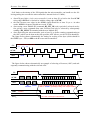
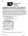
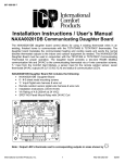
B-sensor User Manual
v1.5 5-April-2001
B-sensor
with addressable
Serial Peripheral Interface
user manual v1.5
5 April 2001
Henk Boterenbrood, NIKHEF, NL
[email protected]
1
B-sensor User Manual
v1.5 5-April-2001
Table of Contents
1
INTRODUCTION.............................................................................................................. 2
2
HOW IT WORKS .............................................................................................................. 3
2.1
2.2
2.3
3
DESCRIPTION .................................................................................................................. 3
PROTOCOL ...................................................................................................................... 5
SIGNAL TIMING .............................................................................................................. 5
SOME TECHNICAL DETAILS ...................................................................................... 7
3.1
3.2
3.3
3.4
ADC CONFIGURATION ................................................................................................... 7
ADC CALIBRATION ........................................................................................................ 8
CONNECTOR PIN-OUT ..................................................................................................... 8
T-SENSOR ....................................................................................................................... 9
1 Introduction
The B-sensor with addressable SPI is a compact module with integrated Hall-sensors on a
PCB containing the 24-bit CRYSTAL CS5524 ADC to digitize the analog signals from the
Hall-sensors, and an ATMEL ATtiny22L (inside there is an AT90LS2343…) 8-bit microcontroller. A picture of the module is shown in Figure 1 with its main components indicated.
The module is connected to the outside world via a so-called Serial Peripheral Interface or
SPI (signals SCLK, SDI and SDO) and a single 'select' signal (CS). Via this serial interface a
controlling system is able to communicate with either the microcontroller or the ADC.
An SPI serial link is a simple point-to-point link but the additional microcontroller provides
the capability to address modules connected to the SPI link, turning the SPI link effectively
into an SPI bus, at the expense of some extra protocol overhead for the controlling system.
← 30 mm →
3x Hall-sensor
NTC temperature-sensor
4-channel ADC
Micro-controller
Multiplexor for
NTC-sensor and its
calibration inputs
↑
56 mm
↓
connector pin 1
Figure 1. The B-sensor module.
← 56 mm →
2
B-sensor User Manual
v1.5 5-April-2001
2 How it works
2.1
Description
Figure 2 below shows schematically a setup between a controlling system and two B-sensor
modules, with only the SPI and microcontroller/ADC interconnection shown.
B-sensor
B-sensor
CRYSTAL
CS5524
24-bit ADC
CRYSTAL
CS5524
24-bit ADC
ACS_
ACS_
SDO
ENA
Controlling
System
(e.g. PC or
µC)
SDI SCLK SDO
SDO
ENA
Atmel
µC
SDI SCLK SDO
CS
Atmel
µC
CS
CS
SDO
SCLK
SDI
Figure 2. A system with two B-sensor modules connected to one SPI interface.
If the microcontroller is present, the CS signal serves to select between microcontroller and
ADC, although an ADC is only accessible after a successful selection protocol with the microcontroller (the microcontroller is in control of the ADC chip-select signal ACS_ ). The
syntax and workings of the selection protocol are explained in the next sections of this document.
(If the microcontroller is not installed some extra resistors have to be mounted, causing CS
to be connected directly to ACS_ so that the controlling system directly controls the ADC
chip-select; also the SDO enable/disable circuit is circumvented. In this case only one Bsensor module can be connected to the SPI interface of the controlling system ! (unless multiple chip-select signals are provided)).
In the rest of this document we assume the microcontroller is present and programmed !
At power-up the B-sensor module goes into the following state: the ADC is not selected
(ACS_ is high) and SDO output (from the ADC) is not enabled (SDO_ENA is low) and the
microcontroller is idle.
Now when CS transitions from low to high the microcontroller wakes up and is ready to receive commands via SDI (clocked via SCLK). So the microcontrollers from all SPI connected B-sensor modules are now listening to the data on the SPI bus.
3
B-sensor User Manual
v1.5 5-April-2001
When CS is taken low again the microcontroller makes ACS_ and SDO_ENA active…or
not, depending on the previously received command(s) and goes back to idle mode (to wake
up again at the next CS transition from low to high). When CS is low the B-sensor is in a
mode where the controlling system can talk to one (single mode, read and write) ADC or all
(broadcast mode, write-only) ADCs, or none, when a non-existent ADC was selected...
When the command(s) to the microcontroller resulted in selection of this B-sensor's ADC
(either in single mode or broadcast mode) the microcontroller makes ACS_ active (enabling
the ADC), before it goes back into idle mode; it makes SDO_ENA active (enabling SDO output from the ADC) only if this B-sensor was selected in single mode; SDO_ENA remains inactive when the ADC was not selected or when broadcast mode has been selected.
In broadcast mode it is possible to access all ADCs simultaneously for writing only, thus
enabling e.g. a simultaneous start of conversion on all connected ADCs. To read out the results of the conversions from the ADCs they must be selected and read out individually, oneby-one. (Note that the ADC requires that the conversion data must be read out !).
The B-sensor is selected in single mode when its Module-ID has been selected or it is selected in broadcast mode when the Broadcast-ID has been selected.
The B-sensor's Module-ID is a one-byte number which is stored in the microcontroller's nonvolatile memory (EEPROM). It must lie between 0 and 127 (7Fh). After production every Bsensor has Module-ID 255 (FFh) and should be set to the required value before use in a multiB-sensor setup. When the module is tested the address is set equal to a serial number shown
on a sticker on the module. The Broadcast-ID is 254 (FEh) and can not be changed.
It is not possible to find out via the SPI interface which Module-ID a B-sensor module has. If
this information somehow gets lost one could find out by connecting the B-sensor to a microcontroller programmer which can read out the microcontroller's EEPROM: the B-sensor's
Module-ID is located in byte 1 of the EEPROM. It could also be set using the programmer.
An alternative way to set a new Module-ID in a B-sensor with an unknown Module-ID is to
connect the B-sensor –on its own– to a controlling system and to set the required B-sensor
Module-ID for every possible Module-ID (one must know the current Module-ID to be able
to change it to a new one…), effectively setting a new ID without knowing the old one.
Details of the protocol between the on-board microcontroller and host system are given in
the next section.
Important:
1) If you have more than one B-sensor module connected to one cable make
sure to disconnect SDO_ENA; it is an output of the B-sensor microcontroller and thus cannot be connected to the same output of other Bsensors! (in modules produced sofar, this pin has been disconnected so
there is nothing to worry about…).
2) Due to a hardware bug in the ATMEL AT90LS2343 microcontroller the
program in the microcontroller does not start up at the first power-up: it
needs to be powered off and soon after (within seconds) powered on
again, only then the program will start running !
4
B-sensor User Manual
2.2
v1.5 5-April-2001
Protocol
A message to the microcontroller always consists of a sync-byte, a command byte and one or
two data bytes. A correctly received sync-byte hopefully ensures correct reception of the rest
of the message
The table below summarizes the possible byte-sequences between controlling system and the
B-sensor's microcontroller. Once an ADC has been selected communication is directly to the
selected ADC; the B-sensor's microcontroller has become transparent. A description of the
communication protocol of the ADC can be found in the CS5524 ADC datasheet.
Byte 0
SYNC
SYNC
Byte 1
BS_SELECT
BS_SELECT
Byte 2
Byte 3
–
–
ModID
BS_BRC_ID
ModID
NewModID
SYNC
BS_SET_ID
with:
SYNC
= F5h
BS_SELECT = 11h
BS_SET_ID = 21h
BS_BRC_ID = FEh
and: 0 ≤ ModID ≤ 127, 0 ≤ NewModID ≤ 127
ACS_/SDO_ENA
(after CS goes low)
ACS_/SDO_ENA active
ACS_ active,
SDO_ENA inactive
ACS_/SDO_ENA inactive
If several messages are sent in a row (leaving CS high) only the first one is read/accepted
and the rest ignored !
So individual messages to the microcontroller must be separated by taking CS low and then
high again.
A sequence of bits and bytes sent to the microcontroller can be interrupted at anytime, but in
order to synchronize the microcontroller for a new message CS should be taken low and then
high again.
2.3
Signal Timing
The relative timings between CS, SDI and SCLK for communication with the microcontroller is the same as for the ADC (CS5524); see for a picture the figure labeled "SDI Write Timing" in the CS5521/22/23/24/28 datasheet.
However the absolute timings of the signals must be far greater when communicating with
the microcontroller than when communicating with the ADC. This is because the protocol is
implemented in software and the microcontroller runs on a clock of only 1 MHz.
5
B-sensor User Manual
v1.5 5-April-2001
Safe limits to the timing of the SPI signals that the microcontroller can handle are the following (taking into account the microcontroller's internal clock of 1 MHz):
•
after CS goes high (='select microcontroller') wait at least 50 µs before the first SCLK
rising edge; SDI data is 'clocked in' with the rising edge of SCLK.
• the time between two edges in the SCLK signal should be at least 30 µs or -in other
words- SCLK's frequency should not exceed 16 kHz.
• after setting a new Module-ID (command BS_SET_ID) wait a period of at least 4 ms before giving a new command (that same B-sensor can only be selected by subsequently
sending a BS_SELECT command with the new Module-ID).
• after deselecting the microcontroller wait at least 30 µs before starting communicating to
the ADC (which can be done at the full speed the ADC allows; see the CS5524 datasheet).
The figure below shows schematically the timing for writing a first byte (which should be
the SYNC byte = F5h) on SDI to the B-sensor microcontrollers.
CS
all microcontrollers selected
50µs
30µs
30µs
SCLK
SDI
MSB
LSB
The figure below shows schematically an example of selecting a B-sensor (ADC) and subsequently communicating with the selected ADC.
CS
all microcontrollers selected
30µs
SCLK
SDI
byte 0
SYNC
SDO
ACS_
byte 1
byte 2
BS_
ModID
SELECT
…now communicating directly with B-sensor ADC with
address 'ModID'; probably reading some output on SDO…
tristated
one ADC selected for read and write
6
B-sensor User Manual
v1.5 5-April-2001
The figure below shows schematically an example of selecting B-sensors (ADCs) broadcast
mode and subsequently writing to all selected ADCs.
all microcontrollers selected
CS
SCLK
SDI
SYNC
BS_
BS_
SELECT BRC_ID
SDO
…now communicating directly with all B-sensor ADCs
but for writing only ! (e.g. a conversion command)…
…SDO remains tristated…
…all ADCs selected…
ACS_
3 Some Technical Details
3.1
ADC Configuration
The ADC on the B-sensor module (24-bit CRYSTAL CS5524) has 4 inputs, called AIN1,
AIN2, AIN3 and AIN4.
Hall-sensor H1 (in picture the top one) is read out on input AIN1, Hall-sensor H2 (in picture
the bottom one) is read out on input AIN2 and Hall-sensor H3 (in picture to the right of the
other 2) is read out on input AIN3.
Input AIN4 is used to read the NTC-sensor and its 2 calibration inputs, using a multiplexor
and the ADC's 2 output latches A0 and A1, shown below in Table 1.
Input AIN4 also provides access to a full-scale calibration input for the Hall-sensor inputs.
AIN
1
2
3
4
Table 1.
Input
Comment
A1A0
–
–
–
00
Hall H1
Hall H2
Hall H3
current monitor
01
10
11
NTC
0º C calib input
100º C calib input
ca. 87 mV, full-scale calibration input
for Hall sensor inputs
ca. 0.43 V ≤ value ≤ 2.43 V
ca. 0.43 V (see section 3.4)
ca. 2.43 V (see section 3.4)
Input channels connected to the B-sensor ADC inputs.
7
B-sensor User Manual
v1.5 5-April-2001
AIN1, AIN2 and AIN3 are used in the 100 mV ADC input range, bipolar.
AIN4 is used in the 2.5V ADC input range, unipolar (Note that in order to read AIN4 with
A1A0=00 (the 87 mV input), the input range and calibration must be adjusted).
The ADC's Charge Pump must be enabled (this is the power-up default).
3.2
ADC Calibration
• Hall-sensor calibration procedure:
o perform a Self Offset calibration on each of the 3 Hall sensor inputs AIN1, AIN2 and
AIN3, and also AIN4, voltage range 100 mV, A1A0 mux-setting irrelevant.
o perform a System Gain calibration on AIN4 with mux-setting A1A0=00, thus selecting the current monitor input, voltage range 100 mV; the resulting gain value is read
from the AIN4 Gain Register and copied to the Gain Registers of inputs AIN1, AIN2
and AIN3.
• T-sensor calibration procedure (resulting in a 16-bits ADC value of 0x0000 at 0ºC and
0xFFFF at 100 ºC):
o perform a System Offset calibration on AIN4 using mux-setting A1A0=10 thus selecting the 0 ºC offset calibration input, voltage range 2.5V.
o perform a System Gain calibration on AIN4 using mux-setting A1A0=11 thus selecting the 100 ºC full-scale calibration input, voltage range 2.5V (now the AIN4 Gain
Register has the proper value for the NTC-sensor read-out).
3.3
Connector Pin-out
Table 2 shows the B-sensor module's connector pin-out configuration for normal operation
(Read-out) and for In-System-Programming of the module's microcontroller.
Pin
Read-out
In-System-Programming
1
2
3
4
5
6
7
8
9
10
SCLK
GND
SDI
GND
SDO
GND
CS
SDO_ENA
–
V+
SCK
GND
–
GND
–
GND
MISO
MOSI
RESET
V+
Table 2.
B-sensor module connector pin-out.
8
B-sensor User Manual
3.4
v1.5 5-April-2001
T-sensor
The T-sensor is an NTC, type number DC95F502W, with a nominal resistance of 5 kΩ. The
table below shows a list of resistance values for this NTC at different temperatures, and the
resulting B-sensor module ADC input voltage, with R14=23.2 kΩ, Vcc=5V and Vref=2.5V. In
the shaded part of the table (between 0 and 70º C) the precision is ±0.2º C.
Temperature
[C]
-50
-45
-40
-35
-30
-25
-20
-15
-10
-5
0
5
10
15
20
25
30
35
40
45
50
55
60
65
70
75
80
85
90
95
100
105
110
115
120
125
Table 3.
Normalized
Resistance
Ohm
68.60
48.16
34.23
24.62
17.91
13.17
9.782
7.339
5.558
4.247
3.274
2.544
1.992
1.572
1.250
1.000
0.8056
0.6530
0.5326
0.4369
0.3604
0.2989
0.2491
0.2087
0.1756
0.1485
0.1261
0.1075
0.09209
0.07916
0.06831
0.05916
0.05141
0.04483
0.03922
0.03442
Resistance
Ohm
343000.00
240800.00
171150.00
123100.00
89550.00
65850.00
48910.00
36695.00
27790.00
21235.00
16370.00
12720.00
9960.00
7860.00
6250.00
5000.00
4028.00
3265.00
2663.00
2184.50
1802.00
1494.50
1245.50
1043.50
878.00
742.50
630.50
537.50
460.45
395.80
341.55
295.80
257.05
224.15
196.10
172.10
AIN4
(ADC)
Volt
-2.1832
-2.0606
-1.9031
-1.7071
-1.4712
-1.1974
-0.8913
-0.5633
-0.2250
0.1106
0.4315
0.7294
0.9982
1.2347
1.4389
1.6135
1.7603
1.8831
1.9852
2.0697
2.1396
2.1974
2.2452
2.2848
2.3177
2.3449
2.3677
2.3868
2.4027
2.4161
2.4275
2.4371
2.4452
2.4522
2.4581
2.4632
NTC resistance/temperature table, and resulting ADC input voltage.
9


![TSD Series -40C ULT User Manual [EN]](http://vs1.manualzilla.com/store/data/005634658_1-66c9db561a67486106446026c707a26c-150x150.png)