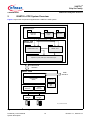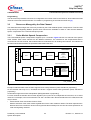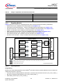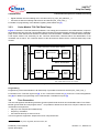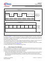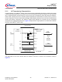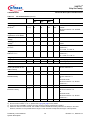
1
M ar c h 2 00 6
L
V INE T I C ®
Communication Solutions
on
A
ND
th
wi
n
io
st
Di
C
O
S y s t e m D e s c r ip t i o n
R e v is i o n 1 . 1
rib
N
User’s Manual
ut
P re li m in ar y
F
ID
E
N
T
V I N E T I C ®-2 CP E ( P E B 3 33 2) , V e rs i on 2. 1
V I N E T I C ®-1 CP E ( P E B 3 33 1) , V e rs i on 2. 1
S LI C - D C( P E F 42 68 ), V er s io n 1 . 2
S LI C - E ( P E F 4 2 65 ), V er s io n 2 . 1
T S LI C - E ( P E F 4 36 5) , V er s io n 2 . 1
V I N E T I C ®-C P E D ev i c e D r iv e r
ly
IA
V oi c e a nd Int er ne t En ha nce d T e le ph on y Inte rfa c e Ci rcu it
Edition 2006-03-13
Published by
Infineon Technologies AG
81726 München, Germany
© Infineon Technologies AG 3/13/06.
All Rights Reserved.
Legal Disclaimer
The information given in this document shall in no event be regarded as a guarantee of conditions or
characteristics (“Beschaffenheitsgarantie”). With respect to any examples or hints given herein, any typical values
stated herein and/or any information regarding the application of the device, Infineon Technologies hereby
disclaims any and all warranties and liabilities of any kind, including without limitation warranties of
non-infringement of intellectual property rights of any third party.
Information
For further information on technology, delivery terms and conditions and prices please contact your nearest
Infineon Technologies Office (www.infineon.com).
Warnings
Due to technical requirements components may contain dangerous substances. For information on the types in
question please contact your nearest Infineon Technologies Office.
Infineon Technologies Components may only be used in life-support devices or systems with the express written
approval of Infineon Technologies, if a failure of such components can reasonably be expected to cause the failure
of that life-support device or system, or to affect the safety or effectiveness of that device or system. Life support
devices or systems are intended to be implanted in the human body, or to support and/or maintain and sustain
and/or protect human life. If they fail, it is reasonable to assume that the health of the user or other persons may
be endangered.
VINETIC® Voice and Internet Enhanced Telephony Interface Circuit
CONFIDENTIAL
Revision History: 2006-03-13, Revision 1.1
Previous Version: Revision 1.0
Page
Subjects (major changes since last revision)
all
Change of naming: Replace term “VINETIC®-CPE Version 2.1 Device Driver” by “VINETIC®-CPE
Device Driver”
Page 38
Update description on UTG, change coefficient names
F_1...F_4 to freqA...freqD and
LEV_1...LEV_4 to levelA ... levelD.
Page 76
Update literature references with latest revision of documents.
Page 51
Update DC Feeding in ACTIVE Mode
Page 54
Upate Transmit Path description
Page 54
Update Impedance Matching and Hybrid description
Page 69
Add TIP-RING Open loop voltage for STANFDBY Mode
Trademarks
ABM®, AOP®, BlueMoon®, ConverGate®, C166®, DuSLIC®, FALC®, GEMINAX®, INCA®, IOM®, IPVD®, Isac®,
IWE®, IWORX®, MuSLIC®, OCTALFALC®, OCTAT®, QUADFALC®, SCOUT®, SEROCCO®, S-GOLD®, SICOFI®,
SIEGET®, SMARTI®, SOCRATES®, VINETIC®, WDTC®, 10BaseS® are registered trademarks of Infineon
Technologies AG.
ACE™, ARCOFI™, ASM™, ASP™, BlueNIX™, DigiTape™, DUALFALC™, EasyPort™, E-GOLD™,
E-GOLDlite™, EPIC™, IPAT-2™, ELIC™, IDEC™, ITAC™, M-GOLD™, SCT™, S-GOLD2™, S-GOLD3™,
MUSAC™, POTSWIRE™, QUAT™, S-GOLDlite™, SICAT™, SIDEC™, SLICOFI™, VDSLite™, 10BaseV™,
10BaseVX™ are trademarks of Infineon Technologies AG.
Microsoft® and Visio® are registered trademarks of Microsoft Corporation. Linux® is a registered trademark of
Linus Torvalds. FrameMaker® is a registered trademark of Adobe Systems Incorporated. APOXI® is a registered
trademark of Comneon GmbH & Co. OHG. PrimeCell®, RealView®, ARM® are registered trademarks of ARM
Limited. OakDSPCore®, TeakLite® DSP Core, OCEM® are registered trademarks of ParthusCeva Inc.
IndoorGPS™, GL-20000™, GL-LN-22™ are trademarks of Global Locate. ARM926EJ-S™, ADS™, Multi-ICE™
are trademarks of ARM Limited.
Template: template_A4_3.0.fm / 3 / 2005-03-10
VINETIC®
Chip Set Family
CONFIDENTIAL
Table of Contents
Table of Contents
Table of Contents . . . . . . . . . . . . . . . . . . . . . . . . . . . . . . . . . . . . . . . . . . . . . . . . . . . . . . . . . . . . . . . . 4
List of Figures . . . . . . . . . . . . . . . . . . . . . . . . . . . . . . . . . . . . . . . . . . . . . . . . . . . . . . . . . . . . . . . . . . . 6
List of Tables . . . . . . . . . . . . . . . . . . . . . . . . . . . . . . . . . . . . . . . . . . . . . . . . . . . . . . . . . . . . . . . . . . . . 7
Preface . . . . . . . . . . . . . . . . . . . . . . . . . . . . . . . . . . . . . . . . . . . . . . . . . . . . . . . . . . . . . . . . . . . . . . . . . 8
1
1.1
1.2
1.3
Introduction . . . . . . . . . . . . . . . . . . . . . . . . . . . . . . . . . . . . . . . . . . . . . . . . . . . . . . . . . . . . . . . . . . . . . 9
Features Overview . . . . . . . . . . . . . . . . . . . . . . . . . . . . . . . . . . . . . . . . . . . . . . . . . . . . . . . . . . . . . . . . 9
Application Examples . . . . . . . . . . . . . . . . . . . . . . . . . . . . . . . . . . . . . . . . . . . . . . . . . . . . . . . . . . . . . 12
User Documentation . . . . . . . . . . . . . . . . . . . . . . . . . . . . . . . . . . . . . . . . . . . . . . . . . . . . . . . . . . . . . . 13
2
2.1
2.1.1
2.1.2
2.1.3
2.2
2.2.1
2.2.2
VINETIC®-CPE System Overview . . . . . . . . . . . . . . . . . . . . . . . . . . . . . . . . . . . . . . . . . . . . . . . . . .
VINETIC®-2CPE/-1CPE Devices . . . . . . . . . . . . . . . . . . . . . . . . . . . . . . . . . . . . . . . . . . . . . . . . . . . .
Physical Interfaces . . . . . . . . . . . . . . . . . . . . . . . . . . . . . . . . . . . . . . . . . . . . . . . . . . . . . . . . . . . . . .
Analog Line Module (ALM) . . . . . . . . . . . . . . . . . . . . . . . . . . . . . . . . . . . . . . . . . . . . . . . . . . . . . . .
Extended Digital Signal Processor (EDSP) . . . . . . . . . . . . . . . . . . . . . . . . . . . . . . . . . . . . . . . . . . .
VINETIC®-CPE Device Driver . . . . . . . . . . . . . . . . . . . . . . . . . . . . . . . . . . . . . . . . . . . . . . . . . . . . . .
Driver Modules and Interface . . . . . . . . . . . . . . . . . . . . . . . . . . . . . . . . . . . . . . . . . . . . . . . . . . . . . .
Driver Interface Structure . . . . . . . . . . . . . . . . . . . . . . . . . . . . . . . . . . . . . . . . . . . . . . . . . . . . . . . . .
15
16
16
17
17
18
18
19
3
3.1
3.2
3.2.1
3.2.2
3.3
3.3.1
3.3.2
3.3.3
3.4
3.5
3.6
3.6.1
3.6.2
3.7
3.7.1
3.7.2
Functional Description Voice/Data Processing . . . . . . . . . . . . . . . . . . . . . . . . . . . . . . . . . . . . . . .
Resource Management . . . . . . . . . . . . . . . . . . . . . . . . . . . . . . . . . . . . . . . . . . . . . . . . . . . . . . . . . . .
Resources Managed by the Phone Channel . . . . . . . . . . . . . . . . . . . . . . . . . . . . . . . . . . . . . . . . . . .
Analog Line Module . . . . . . . . . . . . . . . . . . . . . . . . . . . . . . . . . . . . . . . . . . . . . . . . . . . . . . . . . . . . .
PCM Interface Module . . . . . . . . . . . . . . . . . . . . . . . . . . . . . . . . . . . . . . . . . . . . . . . . . . . . . . . . . . .
Resources Managed by the Data Channel . . . . . . . . . . . . . . . . . . . . . . . . . . . . . . . . . . . . . . . . . . . . .
Coder Module Speech Compression . . . . . . . . . . . . . . . . . . . . . . . . . . . . . . . . . . . . . . . . . . . . . . . .
Signaling Module . . . . . . . . . . . . . . . . . . . . . . . . . . . . . . . . . . . . . . . . . . . . . . . . . . . . . . . . . . . . . . .
Coder Module T.38 FAX Data Pump . . . . . . . . . . . . . . . . . . . . . . . . . . . . . . . . . . . . . . . . . . . . . . . .
Tone Generation . . . . . . . . . . . . . . . . . . . . . . . . . . . . . . . . . . . . . . . . . . . . . . . . . . . . . . . . . . . . . . . . .
Caller Progress Tone Detection . . . . . . . . . . . . . . . . . . . . . . . . . . . . . . . . . . . . . . . . . . . . . . . . . . . . .
Caller ID Support . . . . . . . . . . . . . . . . . . . . . . . . . . . . . . . . . . . . . . . . . . . . . . . . . . . . . . . . . . . . . . . .
Caller ID Transmission . . . . . . . . . . . . . . . . . . . . . . . . . . . . . . . . . . . . . . . . . . . . . . . . . . . . . . . . . .
Caller ID Reception . . . . . . . . . . . . . . . . . . . . . . . . . . . . . . . . . . . . . . . . . . . . . . . . . . . . . . . . . . . . .
Fax/Modem Support . . . . . . . . . . . . . . . . . . . . . . . . . . . . . . . . . . . . . . . . . . . . . . . . . . . . . . . . . . . . . .
Pass Through Mode . . . . . . . . . . . . . . . . . . . . . . . . . . . . . . . . . . . . . . . . . . . . . . . . . . . . . . . . . . . .
T.38 Mode . . . . . . . . . . . . . . . . . . . . . . . . . . . . . . . . . . . . . . . . . . . . . . . . . . . . . . . . . . . . . . . . . . . .
20
20
21
21
22
23
23
25
26
26
27
28
28
29
29
29
29
4
4.1
4.2
4.3
4.3.1
4.3.2
4.3.2.1
4.3.2.2
4.3.3
4.3.3.1
4.3.3.2
4.3.4
4.3.5
Functional Description EDSP Firmware . . . . . . . . . . . . . . . . . . . . . . . . . . . . . . . . . . . . . . . . . . . . .
Host Interface Communication . . . . . . . . . . . . . . . . . . . . . . . . . . . . . . . . . . . . . . . . . . . . . . . . . . . . . .
Resources and Signal Processing Capabilities . . . . . . . . . . . . . . . . . . . . . . . . . . . . . . . . . . . . . . . . .
Firmware Submodule Description . . . . . . . . . . . . . . . . . . . . . . . . . . . . . . . . . . . . . . . . . . . . . . . . . . . .
DTMF Receiver . . . . . . . . . . . . . . . . . . . . . . . . . . . . . . . . . . . . . . . . . . . . . . . . . . . . . . . . . . . . . . . .
Answering Tone Detection (ATD) . . . . . . . . . . . . . . . . . . . . . . . . . . . . . . . . . . . . . . . . . . . . . . . . . .
Answering Tone and Signal Level Detection . . . . . . . . . . . . . . . . . . . . . . . . . . . . . . . . . . . . . . . .
DIS Signal Detection According to T.30 . . . . . . . . . . . . . . . . . . . . . . . . . . . . . . . . . . . . . . . . . . .
Universal Tone Detection (UTD) . . . . . . . . . . . . . . . . . . . . . . . . . . . . . . . . . . . . . . . . . . . . . . . . . . .
Universal Tone and Signal Level Detection . . . . . . . . . . . . . . . . . . . . . . . . . . . . . . . . . . . . . . . . .
V.18 A Detection . . . . . . . . . . . . . . . . . . . . . . . . . . . . . . . . . . . . . . . . . . . . . . . . . . . . . . . . . . . . .
DTMF/AT Generator . . . . . . . . . . . . . . . . . . . . . . . . . . . . . . . . . . . . . . . . . . . . . . . . . . . . . . . . . . . .
Universal Tone Generator (UTG) . . . . . . . . . . . . . . . . . . . . . . . . . . . . . . . . . . . . . . . . . . . . . . . . . .
30
30
31
34
34
35
35
35
36
36
37
38
38
Preliminary User’s Manual
System Description
4
Revision 1.1, 2006-03-13
VINETIC®
Chip Set Family
CONFIDENTIAL
Table of Contents
4.3.6
4.3.7
4.3.8
4.3.9
4.4
4.4.1
4.4.2
4.4.3
4.4.4
Call Progress Tone Detection (CPT) . . . . . . . . . . . . . . . . . . . . . . . . . . . . . . . . . . . . . . . . . . . . . . . .
Caller ID Receiver (CIDR) . . . . . . . . . . . . . . . . . . . . . . . . . . . . . . . . . . . . . . . . . . . . . . . . . . . . . . . .
CID Sender (CIDS) . . . . . . . . . . . . . . . . . . . . . . . . . . . . . . . . . . . . . . . . . . . . . . . . . . . . . . . . . . . . .
Line Echo Cancellation (LEC) . . . . . . . . . . . . . . . . . . . . . . . . . . . . . . . . . . . . . . . . . . . . . . . . . . . . .
Packet Processing . . . . . . . . . . . . . . . . . . . . . . . . . . . . . . . . . . . . . . . . . . . . . . . . . . . . . . . . . . . . . . .
Voice/SID Packets in Downstream Direction . . . . . . . . . . . . . . . . . . . . . . . . . . . . . . . . . . . . . . . . . .
Voice/SID Packets in Upstream Direction . . . . . . . . . . . . . . . . . . . . . . . . . . . . . . . . . . . . . . . . . . . .
Jitter Buffer . . . . . . . . . . . . . . . . . . . . . . . . . . . . . . . . . . . . . . . . . . . . . . . . . . . . . . . . . . . . . . . . . . .
Coder Channel Statistics . . . . . . . . . . . . . . . . . . . . . . . . . . . . . . . . . . . . . . . . . . . . . . . . . . . . . . . . .
39
41
42
43
45
45
46
47
49
5
5.1
5.1.1
5.1.2
5.1.2.1
5.1.2.2
5.1.2.3
5.1.2.4
5.1.3
5.1.3.1
5.1.3.2
5.1.3.3
5.1.4
5.1.5
5.2
5.2.1
5.2.1.1
5.2.1.2
5.2.1.3
5.2.1.4
5.2.1.5
5.2.1.6
5.2.2
5.3
5.3.1
5.3.2
5.3.3
5.3.4
Functional Description POTS Features . . . . . . . . . . . . . . . . . . . . . . . . . . . . . . . . . . . . . . . . . . . . .
BORSCHT Functions . . . . . . . . . . . . . . . . . . . . . . . . . . . . . . . . . . . . . . . . . . . . . . . . . . . . . . . . . . . . .
DC Feeding in ACTIVE Mode . . . . . . . . . . . . . . . . . . . . . . . . . . . . . . . . . . . . . . . . . . . . . . . . . . . . .
AC Transmission Characteristics . . . . . . . . . . . . . . . . . . . . . . . . . . . . . . . . . . . . . . . . . . . . . . . . . . .
Transmit Path . . . . . . . . . . . . . . . . . . . . . . . . . . . . . . . . . . . . . . . . . . . . . . . . . . . . . . . . . . . . . . .
Receive Path . . . . . . . . . . . . . . . . . . . . . . . . . . . . . . . . . . . . . . . . . . . . . . . . . . . . . . . . . . . . . . . .
Impedance Matching and Hybrid . . . . . . . . . . . . . . . . . . . . . . . . . . . . . . . . . . . . . . . . . . . . . . . . .
Howler Tone . . . . . . . . . . . . . . . . . . . . . . . . . . . . . . . . . . . . . . . . . . . . . . . . . . . . . . . . . . . . . . . .
Ringing . . . . . . . . . . . . . . . . . . . . . . . . . . . . . . . . . . . . . . . . . . . . . . . . . . . . . . . . . . . . . . . . . . . . . . .
Ringer Load . . . . . . . . . . . . . . . . . . . . . . . . . . . . . . . . . . . . . . . . . . . . . . . . . . . . . . . . . . . . . . . . .
Ring Trip Detection . . . . . . . . . . . . . . . . . . . . . . . . . . . . . . . . . . . . . . . . . . . . . . . . . . . . . . . . . . .
Internal Balanced Ringing Features . . . . . . . . . . . . . . . . . . . . . . . . . . . . . . . . . . . . . . . . . . . . . .
Off-Hook detection in ACTIVE or STANDBY modes . . . . . . . . . . . . . . . . . . . . . . . . . . . . . . . . . . . .
GR-909 Line Testing . . . . . . . . . . . . . . . . . . . . . . . . . . . . . . . . . . . . . . . . . . . . . . . . . . . . . . . . . . . .
POTS Transmission and Electrical Characteristics . . . . . . . . . . . . . . . . . . . . . . . . . . . . . . . . . . . . . .
AC Transmission Characteristics . . . . . . . . . . . . . . . . . . . . . . . . . . . . . . . . . . . . . . . . . . . . . . . . . . .
Frequency Response . . . . . . . . . . . . . . . . . . . . . . . . . . . . . . . . . . . . . . . . . . . . . . . . . . . . . . . . . .
Gain Tracking (Receive or Transmit) . . . . . . . . . . . . . . . . . . . . . . . . . . . . . . . . . . . . . . . . . . . . . .
Group Delay . . . . . . . . . . . . . . . . . . . . . . . . . . . . . . . . . . . . . . . . . . . . . . . . . . . . . . . . . . . . . . . . .
Out-of-Band Frequency Response (Receive) . . . . . . . . . . . . . . . . . . . . . . . . . . . . . . . . . . . . . . .
Out-of-Band Frequency Response (Transmit) . . . . . . . . . . . . . . . . . . . . . . . . . . . . . . . . . . . . . . .
Total Distortion Measured with Sine Wave . . . . . . . . . . . . . . . . . . . . . . . . . . . . . . . . . . . . . . . . .
DC and Ringing Characteristics . . . . . . . . . . . . . . . . . . . . . . . . . . . . . . . . . . . . . . . . . . . . . . . . . . . .
Application Circuits . . . . . . . . . . . . . . . . . . . . . . . . . . . . . . . . . . . . . . . . . . . . . . . . . . . . . . . . . . . . . . .
Application Circuits for Internal Ringing utilizing SLIC-DC . . . . . . . . . . . . . . . . . . . . . . . . . . . . . . .
Bill of Materials (SLIC-DC Version 1.2) . . . . . . . . . . . . . . . . . . . . . . . . . . . . . . . . . . . . . . . . . . . . . .
Application Circuits for Internal Ringing utilizing SLIC-E . . . . . . . . . . . . . . . . . . . . . . . . . . . . . . . . .
Bill of Materials (SLIC-E Version 2.1) . . . . . . . . . . . . . . . . . . . . . . . . . . . . . . . . . . . . . . . . . . . . . . .
50
50
51
53
54
54
54
55
55
55
56
56
57
57
58
58
65
66
67
67
67
67
69
71
71
72
74
74
Literature References . . . . . . . . . . . . . . . . . . . . . . . . . . . . . . . . . . . . . . . . . . . . . . . . . . . . . . . . . . . . 76
Standards References . . . . . . . . . . . . . . . . . . . . . . . . . . . . . . . . . . . . . . . . . . . . . . . . . . . . . . . . . . . 76
Terminology . . . . . . . . . . . . . . . . . . . . . . . . . . . . . . . . . . . . . . . . . . . . . . . . . . . . . . . . . . . . . . . . . . . 79
Preliminary User’s Manual
System Description
5
Revision 1.1, 2006-03-13
VINETIC®
Chip Set Family
CONFIDENTIAL
List of Figures
List of Figures
Figure 1
Figure 2
Figure 3
Figure 4
Figure 5
Figure 6
Figure 7
Figure 8
Figure 9
Figure 10
Figure 11
Figure 12
Figure 13
Figure 14
Figure 15
Figure 16
Figure 17
Figure 18
Figure 19
Figure 20
Figure 21
Figure 22
Figure 23
Figure 24
Figure 25
Figure 26
Figure 27
Figure 28
Figure 29
Figure 30
Figure 31
Figure 32
Figure 33
Application Example . . . . . . . . . . . . . . . . . . . . . . . . . . . . . . . . . . . . . . . . . . . . . . . . . . . . . . . . . . . .
VINETIC®-2CPE System Overview . . . . . . . . . . . . . . . . . . . . . . . . . . . . . . . . . . . . . . . . . . . . . . . .
Block Diagram of VINETIC®-2CPE/-1CPE . . . . . . . . . . . . . . . . . . . . . . . . . . . . . . . . . . . . . . . . . .
EDSP Firmware Architecture . . . . . . . . . . . . . . . . . . . . . . . . . . . . . . . . . . . . . . . . . . . . . . . . . . . . .
Channel Configuration . . . . . . . . . . . . . . . . . . . . . . . . . . . . . . . . . . . . . . . . . . . . . . . . . . . . . . . . . .
Resource Mapping to Phone Channel and Data Channel Example. . . . . . . . . . . . . . . . . . . . . . . .
PCM Channel . . . . . . . . . . . . . . . . . . . . . . . . . . . . . . . . . . . . . . . . . . . . . . . . . . . . . . . . . . . . . . . . .
Coder Module, Speech Compression. . . . . . . . . . . . . . . . . . . . . . . . . . . . . . . . . . . . . . . . . . . . . . .
Signaling Module . . . . . . . . . . . . . . . . . . . . . . . . . . . . . . . . . . . . . . . . . . . . . . . . . . . . . . . . . . . . . .
Coder Module T.38 FAX Data Pump . . . . . . . . . . . . . . . . . . . . . . . . . . . . . . . . . . . . . . . . . . . . . . .
Simple and Composed Tones . . . . . . . . . . . . . . . . . . . . . . . . . . . . . . . . . . . . . . . . . . . . . . . . . . . .
Block Diagram Host Interface . . . . . . . . . . . . . . . . . . . . . . . . . . . . . . . . . . . . . . . . . . . . . . . . . . . . .
UTD Functional Block Diagram . . . . . . . . . . . . . . . . . . . . . . . . . . . . . . . . . . . . . . . . . . . . . . . . . . .
Universal Tone Generator . . . . . . . . . . . . . . . . . . . . . . . . . . . . . . . . . . . . . . . . . . . . . . . . . . . . . . .
Bellcore On-Hook Caller ID Physical Layer Transmission . . . . . . . . . . . . . . . . . . . . . . . . . . . . . . .
Line Echo Cancellation Module Block Diagram . . . . . . . . . . . . . . . . . . . . . . . . . . . . . . . . . . . . . . .
Signal Paths – DC Feeding . . . . . . . . . . . . . . . . . . . . . . . . . . . . . . . . . . . . . . . . . . . . . . . . . . . . . .
DC Characteristic . . . . . . . . . . . . . . . . . . . . . . . . . . . . . . . . . . . . . . . . . . . . . . . . . . . . . . . . . . . . . .
Signal Paths – AC Transmission . . . . . . . . . . . . . . . . . . . . . . . . . . . . . . . . . . . . . . . . . . . . . . . . . .
Analog Line Module, Signal Flow for an Analog Channel. . . . . . . . . . . . . . . . . . . . . . . . . . . . . . . .
Typical Ringer Loads of 1 and 5 REN According to FCC Part 68 . . . . . . . . . . . . . . . . . . . . . . . . .
Common Faults on POTS lines . . . . . . . . . . . . . . . . . . . . . . . . . . . . . . . . . . . . . . . . . . . . . . . . . . .
Signal Definitions Transmit, Receive . . . . . . . . . . . . . . . . . . . . . . . . . . . . . . . . . . . . . . . . . . . . . . .
Frequency Response Transmit. . . . . . . . . . . . . . . . . . . . . . . . . . . . . . . . . . . . . . . . . . . . . . . . . . . .
Frequency Response Receive . . . . . . . . . . . . . . . . . . . . . . . . . . . . . . . . . . . . . . . . . . . . . . . . . . . .
Gain Tracking Receive . . . . . . . . . . . . . . . . . . . . . . . . . . . . . . . . . . . . . . . . . . . . . . . . . . . . . . . . . .
Gain Tracking Transmit . . . . . . . . . . . . . . . . . . . . . . . . . . . . . . . . . . . . . . . . . . . . . . . . . . . . . . . . .
Group Delay Distortion Receive and Transmit . . . . . . . . . . . . . . . . . . . . . . . . . . . . . . . . . . . . . . . .
Total Distortion Transmit (LX = 0 dBr) . . . . . . . . . . . . . . . . . . . . . . . . . . . . . . . . . . . . . . . . . . . . . . .
Total Distortion Receive (LR = –7 dBr) . . . . . . . . . . . . . . . . . . . . . . . . . . . . . . . . . . . . . . . . . . . . . .
Total Distortion Receive (LR = 0 dBr) . . . . . . . . . . . . . . . . . . . . . . . . . . . . . . . . . . . . . . . . . . . . . . .
Application Circuit Internal Ringing (balanced) for SLIC-DC . . . . . . . . . . . . . . . . . . . . . . . . . . . . .
Application Circuit Internal Ringing (balanced) for SLIC-E . . . . . . . . . . . . . . . . . . . . . . . . . . . . . . .
Preliminary User’s Manual
System Description
6
12
15
16
18
20
21
22
23
25
26
27
30
36
39
43
44
51
52
53
54
56
58
59
65
65
66
66
67
68
68
69
71
74
Revision 1.1, 2006-03-13
VINETIC®
Chip Set Family
CONFIDENTIAL
List of Tables
List of Tables
Table 1
Table 2
Table 3
Table 4
Table 5
Table 6
Table 7
Table 8
Table 9
Table 10
Table 11
Table 12
Table 13
Table 14
Table 15
Supported Features . . . . . . . . . . . . . . . . . . . . . . . . . . . . . . . . . . . . . . . . . . . . . . . . . . . . . . . . . . . . . 9
Delays in Upstream and Downstream Direction . . . . . . . . . . . . . . . . . . . . . . . . . . . . . . . . . . . . . . 25
Provided Algorithms for VINETIC®. . . . . . . . . . . . . . . . . . . . . . . . . . . . . . . . . . . . . . . . . . . . . . . . 31
Typical Ressource Configuration including G.711 and T.38. . . . . . . . . . . . . . . . . . . . . . . . . . . . . 32
Typical Ressource Configuration including complex Coders and T.38 . . . . . . . . . . . . . . . . . . . . 33
Performance Characteristics of the DTMF Receiver Algorithm . . . . . . . . . . . . . . . . . . . . . . . . . . . 34
DFT Length and Window, Frequency Deviation versus Attenuation . . . . . . . . . . . . . . . . . . . . . . . 41
Caller ID Receiver Specifications . . . . . . . . . . . . . . . . . . . . . . . . . . . . . . . . . . . . . . . . . . . . . . . . . 42
FSK Modulation Characteristics . . . . . . . . . . . . . . . . . . . . . . . . . . . . . . . . . . . . . . . . . . . . . . . . . . 43
Maximum Jitter Buffer Size . . . . . . . . . . . . . . . . . . . . . . . . . . . . . . . . . . . . . . . . . . . . . . . . . . . . . . 48
Ringing Options with SLIC-DC and SLIC-E . . . . . . . . . . . . . . . . . . . . . . . . . . . . . . . . . . . . . . . . . 56
AC Transmission . . . . . . . . . . . . . . . . . . . . . . . . . . . . . . . . . . . . . . . . . . . . . . . . . . . . . . . . . . . . . . 60
DC Characteristics . . . . . . . . . . . . . . . . . . . . . . . . . . . . . . . . . . . . . . . . . . . . . . . . . . . . . . . . . . . . . 69
External Components in Application Circuit Internal Ringing - SLIC-DC . . . . . . . . . . . . . . . . . . . . 72
External Components in Application Circuit Internal Ringing - SLIC-E . . . . . . . . . . . . . . . . . . . . . 74
Preliminary User’s Manual
System Description
7
Revision 1.1, 2006-03-13
VINETIC®
Chip Set Family
CONFIDENTIAL
Preface
Preface
This Preliminary User’s Manual System Description documents the system functions and performance
characteristic of the VINETIC®-CPE system (Voice and Internet Enhanced Telephony Interface Concept Customer Premises Equipment).
The VINETIC®-CPE system includes:
•
•
The VINETIC®-CPE chip set consisting of a VINETIC®-2CPE/-1CPE and two/one single channel SLIC-DC
devices or two/one single channel SLIC-E devices.
The VINETIC®-CPE Device Driver.
This user’s manual is part of the VINETIC® documentation package. More VINETIC® related documents are
available via your local Infineon Technologies sales team or the VINETIC® Confidential Library within MyInfineon.
For VINETIC® information available on the web refer to http://www.infineon.com/vinetic.
To simplify matters, the following synonyms are used:
VINETIC®: Synonym used for the codec versions of the VINETIC® CPE family of devices.
SLIC: Synonym used for all SLIC-DC Version 1.2 and SLIC-E Version 2.1.
For detailed information about other VINETIC® devices please refer to the related data sheets.
Attention: TSLIC-E (PEF 4365) is a dual channel version of the SLIC-E (PEF 4265) with identical technical
specifications for each channel. Therefore whenever SLIC-E is mentioned in the specification,
TSLIC-E can also be deployed.
Organization of this Document
This Preliminary User’s Manual System Description is divided into the following chapters:
•
•
•
•
•
•
•
Chapter 1
An introduction of the system package including key features, typical applications and an overview of the
documentation available.
Chapter 2
Overview of HW, SW components, and interfaces supplied with the VINETIC®-CPE system package.
Chapter 3
Functional Description Voice/Data Processing.
Chapter 4
Functional Description EDSP Firmware.
Chapter 5
Functional Description POTS Features.
Literature References
References to related documentation.
Terminology
List of abbreviations and descriptions of symbols.
Preliminary User’s Manual
System Description
8
Revision 1.1, 2006-03-13
VINETIC®
Chip Set Family
CONFIDENTIAL
1
Introduction
Introduction
Infineon’s VINETIC®-CPE system comprise one or two channel analog codecs that are optimized for Customer
Premises Equipment (CPE) as well as Small and Medium Enterprise (SME) VoIP applications.
Featuring an integrated DSP with firmware provided by Infineon, the VINETIC®-CPE system provides a wide
range of flexible VoIP solutions from VoIP CPE to SOHO IP-PBX. VINETIC®-2CPE/-1CPE devices, together with
Infineon’s SLIC-DC or SLIC-E and the VINETIC®-CPE Driver comprise a system package, which can be tailored
to the application with an optimum combination. Chapter 1.1 provides an overview of supported features and
Chapter 1.2 outlines some typical applications, which can be realized with the VINETIC®-CPE system.
1.1
Features Overview
Table 1 lists the features supported by the VINETIC®-CPE system from Infineon at the time this document issue
was prepared. The features depend on the supplied VINETIC®-CPE firmware as well as the VINETIC®-CPE
Device Driver software release. Detailed listing of the supported features with a specific system package can be
found in the latest VINETIC®-CPE System Package Release Note [9].
Table 1
Supported Features
Feature
Channels/
Resources
Restrictions/
Comments
Voice over IP
41)
RTP protocol support
RTP packet statistics (proprietary)
RTCP support
G.711 incl. Appendix I (PLC) and Appendix II (VAD/CNG)
4
G.711 VAD/CNG with noise spectral information
4
G.726 incl. VAD/CNG and BFI error concealment (16, 24, 32,
40 kbit/s)
4
G.723.1 (5.3 kbit/s and 6.3 kbit/s)
4
G.729 Annex A (8 kbit/s) and Annex B
4
G.729 Annex E (11.8 kbit/s)
4
iLBC (13.3 kbit/s and 15.2 kbit/s)
4
PLC is sometimes called BFI
G.726 Coder resources are
overlaid with PCM resources
Line Echo Cancellation exceeding G.165, G.168, G.168-2002: 3
NLEC up to 16 ms tail length
Window based LEC
Voice Play Out (voice packet reordering, fixed and adaptive
jitter buffer, clock synchronization)
4
Connection Control Service
3-Party conferencing via packet network
3-Party conferencing via PCM
3-Party conferencing via PCM and packet network
Voice Mute for Conferencing
Music on hold
Fax Relay
Preliminary User’s Manual
System Description
9
Revision 1.1, 2006-03-13
VINETIC®
Chip Set Family
CONFIDENTIAL
Table 1
Introduction
Supported Features (cont’d)
Feature
Channels/
Resources
Restrictions/
Comments
T.38 support (V.21, V.27ter, V.29 and V.17)
42)
Fax Relay T.38 resources are
overlaid with Coder resources.
T.38 Data Pump implemented in
the VINETIC® system. For full
T.38 functionality some additional
SW is required (Fax Agent and
T.38 stack).
Signaling
Integrated DTMF generator
4
Integrated DTMF decoder
4
Integrated Caller ID (FSK) generator, according to Bellcore 202 4
and V.23
Caller ID receiver
4
Support for FXO-driver on analog and PCM interface
Caller ID (on hook = type 1)
Telcordia/Bellcore
ETSI CID between ring bursts (FSK and DTMF)
ETSI prior to first ring burst (FSK and DTMF - with DTAS, LR or
RP)
SIN 227 (British Telecom)
NTT (Japan)
Caller ID (off hook = type 2)
Telcordia/Bellcore
ETSI (FSK and DTMF)
SIN 227 (British Telecom)
NTT (Japan)
Message Waiting Indication with support of VMWI (FSK)
By integrated Caller ID (FSK)
generator
Call Progress Tone detection (CPT)
4
RFC2833 support for named DTMF events
4
Howler Tones (very high level on analog port)
Universal Tone Generation in up- and downstream
4
One generator per signaling
module
CODEC/SLIC
Worldwide programmability for AC transmission performance
parameters (country specific programming, e.g. AC impedance
matching, hybrid balance, transmit and receive gain, frequency
response) , specification in accordance with ITU-T
Recommendation Q.552 [33] for interface Z and ETSI Standard
ES 202 971 [15]
Integrated sinusoidal balanced ringing capability - software
programmable up to 65 Vrms ringing voltage (depending on
external components), frequency range between 15 and 75 Hz
Loop start signaling
Preliminary User’s Manual
System Description
10
Revision 1.1, 2006-03-13
VINETIC®
Chip Set Family
CONFIDENTIAL
Table 1
Introduction
Supported Features (cont’d)
Feature
Channels/
Resources
Restrictions/
Comments
Polarity reversal
AC Ring Trip detection
Fast Ring Trip detection
Ringing with DC offset
On-hook transmission
PCM Interface G.711 A-law/µ-law
8
PCM Interface 16 bit linear
8
PCM Interface G.726 (16, 24, 32, 40 kbit/s)
4
G.726 Coder resources are
overlaid with PCM resources
Driver/API
Linux
VxWorks
Host Interface
Parallel Host Interface: Intel/Motorola compatible
Serial Control Interface SCI (Infineon), SPI compatible
SPI mode 3 is used (different to
previous chip versions)
Big and little endian support
Miscellaneous
Integrated Test and Diagnostic Functions for local loop
monitoring according to GR-909
Wide band support (16 kHz transmission possible)
Polling access
1) For VINETIC®-1CPE only 2 coder channels are supported.
2) For VINETIC®-1CPE only 2 fax channels are supported
Preliminary User’s Manual
System Description
11
Revision 1.1, 2006-03-13
VINETIC®
Chip Set Family
CONFIDENTIAL
1.2
Introduction
Application Examples
Typical applications utilizing the VINETIC®-CPE system package are:
•
•
•
•
•
Residential Gateways, VoIP Routers, ATAs
Integrated Access Devices (IAD)
VoIP xPON
VoIP Cable Modems, eMTAs, SMTAs
VoIP PBX
Figure 1 depicts two applications of the VINETIC®-CPE system.
Residential Gateway
T/R
VINETIC®
SLIC
Telephone
T/R
Host Controller
ADM5120
8-bit µC bus
VINETIC® -2CPE
Driver
SLIC
Telephone
Flash
Memory
T/R
SLIC
Telephone
SDRAM
WAN
Magnetics
VINETIC® -2CPE
T/R
SLIC
Magnetics
Telephone
Ethernet LAN
Analog Telephony Adapter - ATA/Router
T/R
VINETIC®
SLIC
Telephone
8-bit µC bus
VINETIC® -2CPE
T/R
Driver
Host Controller
ADM5120
SLIC
Telephone
Flash
Memory
SDRAM
Magnetics
Magnetics
Ethernet LAN
CPE_STANDARDAPP
Figure 1
Application Example
Preliminary User’s Manual
System Description
12
Revision 1.1, 2006-03-13
VINETIC®
Chip Set Family
CONFIDENTIAL
1.3
Introduction
User Documentation
The VINETIC®-CPE system is provided with the following user documentation:
VINETIC®-2CPE/-1CPE Version 2.1 Product Brief
A two page overview on product features, tools and applications.
VINETIC®-CPE Version 2.1 Preliminary User’s Manual System Description
This document gives a system overview, outlines the main building blocks of the system and details the system
interfaces. Furthermore the document provides a functional description of the voice/data processing and POTS
features and specifies POTS system performance.
VINETIC®-2CPE/-1CPE (PEB 3332/-3331) Version 2.1, SLIC-DC (PEF 4268) Version 1.2 and
SLIC-E/TSLIC-E (PEF 4265/PEF 4365) Version 2.1 Preliminary Data Sheet Data Sheet
The data sheet provides descriptions on pin layout, pin description, clocking and reset behavior. Additionally it
covers the parallel and serial interfaces, limit values as well as the package outline.
SLIC-E/TSLIC-E (PEF 4265/PEF 4365) Version 2.1 Preliminary Data Sheet
The data sheet provides descriptions on pin layout, pin description. Additionally it covers the parallel and serial
interfaces, limit values as well as the package outline.
VINETIC®-2CPE/-1CPE (PEB 3332/-3331) Version 2.1 Hardware Design Guide
The VINETIC®-2CPE/-1CPE Hardware Design Guide serves as a reference document for the design of
applications using the VINETIC®-2CPE Version 2.1 or VINETIC®-1CPE Version 2.1 together with the SLIC-DC
Version 1.2 and the SLIC-E Version 2.1.
VINETIC®-CPE Device Driver Preliminary User’s Manual Driver and API Description
This user’s manual describes the VINETIC®-CPE Device Driver structure, the software interfaces and provides
examples on the usage of the interfaces.
VINETIC®-CPE Device Driver Porting and Integration Guide Rev. 1.0
This document provides guidance on porting as well as the integration of the VINETIC®-CPE device driver on a
new system with the consideration of target operating system and target hardware.
VINETIC®-CPE System Package Release Notes
The System Package Release Notes provide release information on all system components including:
•
•
•
•
•
VINETIC®-2CPE/-1CPE devices
SLIC devices
VINETIC®-CPE Driver
EDSP firmware
VINETICOS software
VINETIC®-CPE System Errata Sheet
This document lists the know problems of the VINETIC®-CPE system as well as of the associated user
documentation.
Preliminary User’s Manual
System Description
13
Revision 1.1, 2006-03-13
VINETIC®
Chip Set Family
CONFIDENTIAL
Introduction
T.38 Test Application Release 1.0 User's Manual Programmer's Reference
This document describes how to use the T.38 protocol stack together with the T.38 FAX Agent and the Test
Application on the Easy334 Evaluation Board.
The latest revision of the above listed VINETIC®-CPE related user documentation is available via your local
Infineon Technologies sales team or the VINETIC® Confidential Library within MyInfineon.
Preliminary User’s Manual
System Description
14
Revision 1.1, 2006-03-13
VINETIC®
Chip Set Family
CONFIDENTIAL
2
VINETIC®-CPE System Overview
VINETIC®-CPE System Overview
Figure 2 depicts the components supplied with a VINETIC®-CPE system.
HostController
ApplicationLayer
Application
Softw are
T.38 Fax
Agent
T.38 Stack
VINETIC® -CPE
Device Driver
VINETIC Driver API
VINETIC TAPI
Operation System, HW Layer and Board Layer
Parallel /Serial
Interface
VINETIC®-2CPE
PCM
Interface
Host Interface
EDSP
Firmw are
Extended DSP
(EDSP)
BBD
File
Analog Line Module (ALM)
Analog
Channel-A
Analog
Channel-B
SLIC-DC/
SLIC-E
SLIC-DC/
SLIC-E
CPE_SYSTEMOVERVIEW
Figure 2
VINETIC®-2CPE System Overview
Preliminary User’s Manual
System Description
15
Revision 1.1, 2006-03-13
VINETIC®
Chip Set Family
CONFIDENTIAL
VINETIC®-CPE System Overview
The VINETIC®-CPE system package includes:
•
•
•
•
•
•
•
VINETIC®-2CPE/-1CPE devices
SLIC-DC (PEF 4268) / SLIC-E (PEF 4265) devices
VINETIC®-CPE Device Driver, including a VINETIC® Driver API and a TAPI for the host controller
EDSP firmware and BBD (block based download) files
VINETICOS coefficient calculation
FAX Agent (optionally supplied)
VINETIC®-CPE documentation
2.1
VINETIC®-2CPE/-1CPE Devices
Figure 3 depicts the internal structure of the VINETIC®-2CPE/-1CPE devices. The main blocks of the VINETIC®2CPE/-1CPE are:
•
•
•
Analog Line Module (ALM) supporting one (VINETIC®-1CPE) or two (VINETIC®-2CPE) Analog Line Channels
(Channel A and B). The analog line channels provide the interface to the SLIC devices.
Extended Digital Signal Processor (EDSP) with external ROM and RAM for firmware download.
Host Interface providing the parallel, serial, GPIO, PCM as well as the interrupt interface.
Analog line channels, EDSP and host interfaces exchange data via an internal BUS and are synchronized via
the PLL clock control.
164
MHz
PLL,
Clock Control
32 MHz
HostInterface
ANALOG
LINE
MODULE
BUS
164
MHz
ANALOG
CHANNEL
B
SLIC
Serial
Interface
Parallel
Interface
GPIO
PCM
BUS
SLIC
ANALOG
CHANNEL
A
Interrupt
not
available
in PGTQFP-648
HOST
•
JTAG
Extended DSP
(EDSP)
ROM/RAM
not available in 1 channel device
Vinetic_0001_VineticV21_Blockdiagram_2cpe1cpe
Figure 3
Block Diagram of VINETIC®-2CPE/-1CPE
2.1.1
Physical Interfaces
For programming the VINETIC® and for performing packet data transfer from/to the VINETIC®, a parallel interface
or a serial micro controller interface can be used. The selection of the interface is done by means of pin strapping.
Additionally, the VINETIC® has an interface for PCM data. For details on the VINETIC® hardware refer to [2].
8-bit Parallel Interface
•
The parallel interface can be operated in Intel 8-bit mode (multiplexed/demultiplexed) or in 8-bit Motorola
mode.
Preliminary User’s Manual
System Description
16
Revision 1.1, 2006-03-13
VINETIC®
Chip Set Family
CONFIDENTIAL
VINETIC®-CPE System Overview
Serial Interface
•
The VINETIC® serial micro controller interface (µC interface = SCI) is compatible with the Motorola SPI and
the Infineon SCI.
PCM Interface
•
The VINETIC®-2CPE/-1CPE has one PCM interface providing two PCM highways that are internally crossconnected, which allows concurrent operation together with the serial µC interface or the parallel interface.
GPIO Interface
•
The VINETIC® GPIO pins (general purpose IO) provide eight configurable IO pins (GPIO0 - GPIO7) for general
use. The VINETIC® API provides a programming interface for configuration, controlling and reading of the
GPIO pins.
SLIC Interface
•
The SLIC-DC (PEF 4268) Version 1.2 and the SLIC-E (PEF 4265) Version 2.1 are controlled by ternary logic
signals.
Test Interface (JTAG Interface)
•
The JTAG interface for test access is provided.
Detailed documentation to the VINETIC®-2CPE/-1CPE physical interfaces is provided in [2] and [4].
2.1.2
Analog Line Module (ALM)
The analog line module carries one or two analog line channels. One channel is shown in Figure 20. Each analog
channel consists of an analog front end and a digital front end. The digital front end is configured via the BBD-file,
generated by the VINETICOS tool. This provides flexible adjustment to the connected analog lines, for example
to adapt the system to country specific or customer specific requirements. The BBD-file contains all information to
adjust the digital front end of the VINETIC®-2CPE/-1CPE to country specific parameters. The following functions
are configured via this file:
•
•
•
•
•
•
Impedance Matching
Hybrid
Gain Adjustment
Frequency Response
Ringing
Ring Trip Thresholds
The analog line module can be accessed via the structure Phone Channel (for details see [3]) of the device driver.
2.1.3
Extended Digital Signal Processor (EDSP)
Figure 4 illustrates the module concept for a VINETIC®-2CPE device. The number of supported PCM channels,
analog channels and coder channels is dependent on the device type. The VINETIC®-2CPE/-1CPE EDSP has a
modular firmware concept, providing four different types of firmware modules:
•
•
•
PCM-Interface-Module, covering the connection to the PCM interface of a signal provided by the analog
channel or by a coder channel. The PCM interface can be configured and operated via the Phone Channel the
device driver.
ALM-Interface-Module, responsible for the interface to the analog line channel of the ALM. The ALM-InterfaceModule and the respective analog-line-channel can be accessed via the entity Phone Channel of the device
driver.
The Coder Module supports two different types of channels. One type of channel is optimized for speech
compression, the second type of channel is optimized for a FAX data pump.
Preliminary User’s Manual
System Description
17
Revision 1.1, 2006-03-13
VINETIC®
Chip Set Family
CONFIDENTIAL
PCMInterface
HostInterface
0
ALM-Out
I1..5
ALM
Interface
Module
PCM
Interface
Module
0
1
Figure 4
0
HostInterface
Signaling-Module, carrying different signal generation and detection submodules.
Analog Line
Channel
•
VINETIC®-CPE System Overview
InterConnection
Signaling
Module
Coder
Module
0
EDSP Firmware Architecture
The VINETIC®-CPE Device Driver provides the software interface for the application software, running on the host
controller, to perform the required configuration work for each module as well as for managing interconnection
between the modules. Coder Module and Signaling Module are configured and controlled via the Data Channel
structure (see Chapter 2.2.2) of the VINETIC® device driver. Further detailed information on connection control
and operation control is provided in Chapter 3.1 and in [3].
2.2
VINETIC®-CPE Device Driver
2.2.1
Driver Modules and Interface
Detailed documentation for the VINETIC®-CPE Device Driver and API, including compilation, initialization and
program interface descriptions, is provided in [3] and [5]. The driver provides the following software modules and
interfaces:
OS-Layer
•
An operating system abstraction layer encapsulates specifics of different operating systems. In case you want
to operate the VINETIC®-CPE with another operating system only this module must be modified. For details
on porting of the driver refer to [5].
HW-Layer and Board Layer
•
Board specific code has been eliminated from the VINETIC®-CPE device driver and must be provided by the
BSP or a separate board driver. This includes the reset line, configuration of the memory or SPI controller and
other board specific code.
VINETIC® Driver API (Non TAPI Interfaces)
Device specific functionality and read / write interface. This API is split into the following group of interfaces:
•
•
•
•
•
Polling Interface
Basic Interface
Driver Initialization Interface
GPIO Interface
Driver Kernel Interfaces
Preliminary User’s Manual
System Description
18
Revision 1.1, 2006-03-13
VINETIC®
Chip Set Family
CONFIDENTIAL
VINETIC®-CPE System Overview
Telephony API (TAPI)
Driver components which provide an API for the handling of the VINETIC® telephony functionality. The TAPI is
split into different services:
•
•
•
•
•
•
•
•
•
•
•
•
•
Initialization Service
Operation Control Service
Metering Service
Tone Control Service
Dial Service Signal
Detection Service
CID Features Service
Connection Control Service
Miscellaneous Services
Ringing Service
PCM Service
Fax T.38 Service
Call on Hold Support Service
2.2.2
Driver Interface Structure
To configure and control the different resources of the VINETIC®-2CPE/-1CPE device the VINETIC®-CPE Device
Driver provides a powerful service structure. The driver maps the VINETIC®-2CPE/-1CPE resources (Analog Line
Channel, PCM Interface Module, Coder Module, Signaling Module and LEC submodule) to either a Phone
Channel or a Data Channel structure, which can be configured and controlled via TAPI.
The VINETIC®-CPE Device Driver provides the following two main software constructs to configure and control
the resources provided by the VINETIC®-2CPE/-1CPE device on a channel basis:
•
•
The Phone Channel provides management of the Analog Line Channel of the Analog Line Module and also
for the PCM Channels of the PCM Interface Module.
The Data Channel represents the combination of the coder channel module and the associated signaling
module of the EDSP. The data channel supports two different types of coders. One coder is optimized for
speech compression, which is described in Chapter 3.3.1. The second type of coder is optimized for a FAX
data pump and is documented in Chapter 3.3.3. The signaling module is detailed in Chapter 3.3.2.
Each phone channel and each data channel as well as the device itself are mapped to device nodes of the
operating system on the host controller. The driver provides access to the resources of the VINETIC®-2CPE/1CPE via a channel specific nodes (/dev/vin11, /dev/vin12). For details see [3]. Additionally services are provided
which apply to the complete devices. These services are addressed via the device-specific nodes (for example
\dev\vin10):
•
•
GPIO Interface Service to control and monitor the GPIO pins of the VINETIC®-2CPE/-1CPE devices.
Service to assigne the PCM time slots to the PCM Channels.
Note: The application accesses phone and data channel of one ressource number via one specific device node although phone channel and data channel of one ressource number must not necessarily be connected to
each other.
Preliminary User’s Manual
System Description
19
Revision 1.1, 2006-03-13
VINETIC®
Chip Set Family
CONFIDENTIAL
Functional Description Voice/Data Processing
3
Functional Description Voice/Data Processing
3.1
Resource Management
Figure 5 shows three examples of channel configurations which can be established with the VINETIC®-CPE
system. The available resources (PCM, Signaling, Coder, and Analog Lines) of the VINETIC®-2CPE device and
the usage of the device resources by the different calls are indicated.
VoIP
C
B
DuSLIC-S
Chipset
Host
Controller
IP
Network
A
C
Voice
Samples
RTP
PCM
Interface
Host
Interface
PCM3
PCM2
PCM1
PCM0
SIG3
SIG2
SIG1
SIG0
COD3
COD2
COD1
COD0
ALM1
ALM0
SLIC
SLIC
A - VoIP Call without PCM
B - Call switched over PCM
C - VoIP Call over PCM
VINETIC® Device
PCM0 - PCM3: PCM Interface Modules
SIG0 - SIG3: Signaling Modules
COD0 - COD3: Coder Modules
ALM0 - ALM1: Analog Line Modules
B
Figure 5
A
CPE_CHANNEL_CONFIGURATION
Channel Configuration
In order to configure a connection and to provide effective management of the associated VINETIC®-CPE
resources to the application software, the VINETIC®-CPE Device Driver provides the Phone Channel and Data
Channel structures.
Thus a distinction is made on the interface to the application software between:
•
•
Data Channel resources in charge of complex signal processing (such as speech compression, signal
generation/detection and packetization) and
Phone Channel resources (PCM Interface and Analog Line Interface) seen as a kind of I/O port for the digitized
voice.
Preliminary User’s Manual
System Description
20
Revision 1.1, 2006-03-13
VINETIC®
Chip Set Family
CONFIDENTIAL
Functional Description Voice/Data Processing
Figure 6 depicts the mapping of the device resources to the Phone Channel and to the Data Channel for the
examples shown in Figure 5.
Note: Additional to the above configuration conferencing between the different participants is supported.
Analog Line
Module
Channel A
Coder
Module
Channel 0
ALM0
SIG0
COD0
Phone Channel 1
Signaling
Module
Channel 0
Data Channel 1
Node:dev\vin11
Path A
Analog Line
Module
Channel B
ALM1
Coder
Module
Channel 1
PCM
Interface
Module
Channel 2
COD1
PCM2
Phone Channel 2
Signaling
Module
Channel 1
SIG1
Data Channel 2
Node:dev\vin12
Path B
Coder
Module
Channel 3
PCM
Interface
Module
Channel 3
COD3
PCM3
Phone Channel 3
Signaling
Module
Channel 3
SIG3
Data Channel 3
Node:dev\vin13
Path C
CPE_CHANNEL_CONFIGURATION_DRV
Figure 6
Resource Mapping to Phone Channel and Data Channel Example
3.2
Resources Managed by the Phone Channel
The phone channel manages the resources provided by the Analog Line Module and the PCM Interface Module
as well as the LEC module, which may be utilized by the Analog Line Module as well as by the PCM Interface
Module.
3.2.1
Analog Line Module
Figure 20 shows one analog channel of the analog line module in a VINETIC®-CPE system. The module consists
of the following submodules:
•
•
Analog front end (AFE) including the ADC, DAC, impedance matching, pre and post filters.
Digital front end including impedance matching, transmit/receive amplifier, transhybrid filter and frequency
response filters. These submodules are configured via the BBD-file towards country specific parameters.The
coefficients can be computed and converted to the BBD-file format with the VINETICOS tool.
Preliminary User’s Manual
System Description
21
Revision 1.1, 2006-03-13
VINETIC®
Chip Set Family
CONFIDENTIAL
•
Functional Description Voice/Data Processing
Furthermore the digital front end incorporates gain stages for the receive (Gain2) and transmit (Gain1) path to
allow a gain adjustment of the respective path. Beside the gain stages a LEC submodule can be used to cancel
a near end echo. A detailed description of the LEC submodule is given in Chapter 4.3.9. Gain stages as well
as the LEC submodule can be configured by the application software via the specific TAPI interface.
Programming
The device driver provides the services for configuration and control of the Phone Channel, which utilizes the
Analog Line Channels of the Analog Line Module. For details on programming of the Analog Line Channels see
[3].
3.2.2
PCM Interface Module
The PCM Interface Module of the VINETIC®-CPE device supports up to 4 PCM channels. Figure 7 shows one
channel of the PCM Interface Module respectively. Each PCM channel can be separately activated via the
associated Phone Channel and provides the following submodules:
•
•
•
•
•
•
A G.711/G.726/Linear Submodule provides the coding/decoding algorithm for G.711 (A/µ -Law), G726
(ADPCM) (G.726 - 16 kbit/s, 24 kbit/s, 32 kbit/s, 40 kbit/s) and linear coding (16 bit).
An Adder provides conferencing by just adding up to five input signals.
The submodules Gain1 and Gain2 allow a gain adjustment of the transmit and receive path.
The High Pass Submodule (HP), cutoff frequency below 20 Hz, drops the DC part of the signal. Especially the
DC part of a signal would decrease the performance of the LEC significantly when a LEC is used.
The LEC submodule can be used to cancel a near end echo. A detailed description of the configuration and
operational control of the LEC submodule is given in Chapter 4.3.9.
The RBS (Robbed bit signaling) module suppresses signaling information. It replaces the signaling information
with a constant pattern. The RBS module modifies the received PCM values and has therefore to be in front
of the PCM decoder.
PCM Channel
I1
I3
I4
ADDER
I2
G.711 /
G.726 /
Linear
Gain 1
PCM-Interface
I5
NearEnd
LEC
PCM-Out
Gain 2
-
HP
G.711 /
G.726 /
Linear
RBS
CPE_PCM_MODULE
Figure 7
PCM Channel
Preliminary User’s Manual
System Description
22
Revision 1.1, 2006-03-13
VINETIC®
Chip Set Family
CONFIDENTIAL
Functional Description Voice/Data Processing
Programming
The device driver provides the services for configuration and control of the Phone Channel, which utilizes the PCM
channels of the PCM Interface Module. For details on programming of the PCM channels see [3].
3.3
Resources Managed by the Data Channel
The Data Channel manages the resources provided by the Coder Module Speech Compression/ T.38 Fax Data
Pump and by the Signaling Module. Specific driver services are available to switch a coder channel between
speech compression and T.38 FAX data pump mode.
3.3.1
Coder Module Speech Compression
The Coder Module Speech Compression supports up to 4 channels. Figure 8 shows one channel of the speech
coder module. Each coder channel has two different interfaces. The interface for the sample-based side is
connected to a Phone Channel, which utilizes either a PCM Channel or an Analog Line Channel. The interface on
the frame-based side transfers the packetized data toward the host.
Coder-Module
I1
I4
AGC
Gain 1
Packetized
Voice
Protocol
Unit
Encoder
RTP(TCP/IP)
I5
Voice Play Out Unit
Gain 2
Decoder
HP
Jitter
Buffer
Depacketized
Voice
Protocol Unit
Host Interface (Packets)
I3
ADDER
I2
RTP(TCP/IP)
CPE_CODER_MODULE
Figure 8
Coder Module, Speech Compression
Except G.729E and iLBC each encoder supports voice activity detection (VAD, standard or proprietary).
On the decoder side only G.711, G.729A,B and G.723.1 support comfort noise generation (CNG, standard or
proprietary).
All decoders support bad frame manipulation (BFM) (standard or proprietary).
For each channel the decoder and encoder algorithm (G.7xx) can be set, independent of each other, on an active
channel. For example, in the receive direction a G.723.1 decoder and in the transmit direction a G.729A,B encoder
may be active.
•
Coder Module Timer and Coder Channel Timer
With the activation of the coder module a global timer for the coder module is started. The timer represents the
absolute time for the VINETIC® and is used to generate the timestamps for the voice and event packets for all
coder and signaling channels.
Preliminary User’s Manual
System Description
23
Revision 1.1, 2006-03-13
VINETIC®
Chip Set Family
CONFIDENTIAL
•
•
•
•
•
•
•
•
Functional Description Voice/Data Processing
Each coder channel has its own channel timer for the decoder direction. In case of RTP packets the channel
timer is used by the corresponding signaling channel to synchronize the events with the voice stream.
Automatic Gain Control (AGC) Submodule
The AGC (Automatic Gain Control), which is placed after the input adder, could be used to gain and/or to limit
the level of the input signal. The limitation should prevent the clipping of the signal as especially low bit rate
encoders have problems with clipped signals (due to the high frequency parts). To prevent clipping, the system
designer should reduce the input gains of the analog line interfaces, for example by 6 dB, and should
compensate the 6 dB with the AGC. The AGC can be placed after the coder as well.
Subsubmodulemodules Gain1 and Gain2 allow a gain adjustment of the transmit and receive path. These
blocks can adjust the signals to and from the signal array, e.g. for conferencing. Gain1 and Gain2 can be
adjusted via the driver service IFX_TAPI_ENC_VOLUME_SET/IFX_TAPI_DEC_VOLUME_SET.
The ADDER submodule easily allows conferencing by just adding up to five signals from a PCM or phone
interface.
The High Pass (HP) submodule (cutoff frequency below 20 Hz) drops the DC part of the signal. Especially
when using a LEC the DC part of a signal would significantly decrease the performance of the LEC.
Packetized Voice Protocol Unit (PVPU)
In upstream direction the Packetized Voice Protocol Unit gets the frames from the encoder and composes the
payload. When the payload has the desired packet time the PVPU adds the header to the voice or SID data
and sends the packet to the host.
The PVPU supports also the RTCP sender report with the RTP protocol support.
Depacketized Voice Protocol Unit (DVPU)
The Depacketized Voice Protocol Unit (DVPU) is part of the Voice Play Out Unit and is responsible for
validation checks, packet decomposing, packet reordering, and to support the RTCP sender statistic.
Voice Play-Out Unit (VPOU)
The Voice Play Out Unit (VPOU) is responsible for:
– Packet validation checks
– Packet decomposing
– Reordering
– Estimation and resizing of the jitter buffer (for detailed description see Chapter 4.4.3)
– Clock synchronization
– Play out of received packets
– RTCP receiver statistic
When the VPOU readjusts the jitter buffer it passes the information about the playout delay adjustment to the
LEC. Therefore the LEC must not perform a completely re-adaptation due to the alteration of the play out delay.
Programming
Programming of the Coder Module Speech Compression is provided via driver services:
•
•
•
For the decoder (IFX_TAPI_DEC_*)
For the encoder (IFX_TAPI_DEC_*) and
For the jitter buffer (IFX_TAPI_JB_*)
For details on programming of the Coder Module Speech Compression see [3].
Delays
In upstream direction, generally, the delay is determined by the packet size of the codec as listed in Table 2 plus
an additional delay of up to one frame depending on the IM-bit setting. In downstream direction the minimum delay
is given through the chosen packet size (PTE) plus the delays created by the jitter buffer and an additional 0.5 ms
buffer to handle EDSP overload situations.
Preliminary User’s Manual
System Description
24
Revision 1.1, 2006-03-13
VINETIC®
Chip Set Family
CONFIDENTIAL
Table 2
Functional Description Voice/Data Processing
Delays in Upstream and Downstream Direction
Coder
Packet Size
G.711, G.726
2.5 ms
G.723.1
30 ms
G.729
10 ms
iLBC
20/30 ms
3.3.2
Signaling Module
Figure 9 depicts one channel of a Signaling Module. Each channel provides the following submodules:
•
•
•
•
•
•
•
•
DTMF Receiver (for a detailed functional description see Chapter 4.3.1)
Answering Tone and DIS Detection - ATD (for a detailed functional description see Chapter 4.3.2)
Universal Tone and V.18 A Detection - UTD (for a detailed functional description see Chapter 4.3.3)
DTMF / AT Generation (for a detailed functional description see Chapter 4.3.4)
Calling Progress Tone Detector - CPT (for a detailed functional description see Chapter 4.3.6)
FSK (Caller ID) Receiver (for a detailed functional description see Chapter 4.3.7)
FSK (Caller ID) Sender (for a detailed functional description see Chapter 4.3.8)
Universal Tone Generator - UTG (for a detailed functional description see Chapter 4.3.5)
CID
Sender
Status
CID-Receiver
Status
Event
Event
Figure 9
DTMF / AT /
Tone Generator
DTMF-Receiver
Status
Event
CPT
Status
ATD (2x)
Status
Status
Event
UTD (2x)
Status
Coder
Module
Phone Channel
UTG
Event
Trans./
Play Out
Host Interface
Signaling Module
Status
Status
Channel status information reflected in TAPI channel status struture (IFX_TAPI_CH_STATUS_t)
Event
Downstream RTP Event Packets
Event
Upstream RTP Event Packets
CPE_SIGNALING_MODULE
Signaling Module
Programming
Based on the submodules listed above the VINETIC®-CPE Device Driver provides different services to utilize the
implemented functions. These are:
•
•
•
Tone play services, utilizing DTMF/AT Generation, Universal Tone Generator and CPT: (IFX_TAPI_TONE_*)
Dial services utilizing DTMF Dedector (IFX_TAPI_TONE_DTMF_*)
Pulse dialing services (IFX_TAPI_PULSE_*)
Preliminary User’s Manual
System Description
25
Revision 1.1, 2006-03-13
VINETIC®
Chip Set Family
CONFIDENTIAL
•
•
Functional Description Voice/Data Processing
Signal detection services utilizing ATD, UTD and CPT (FX_TAPI_SIG_DETECT_*)
CID services Services utilizing CID Receiver and Sender (IFX_TAPI_CID_*)
For details on programming of the different signaling submodules see [3].
3.3.3
Coder Module T.38 FAX Data Pump
Figure 10 shows the T.38 FAX Data Pump Module. The analog phone interface or the PCM interface is input for
the upstream direction (encoder / demodulator path) and output for the downstream direction (decoder / modulator
path). On the other side the host interface is interface to the demodulator, modulator, encoder and decoder path.
A full duplex mode is not necessary for the T.38 FAX transmission, therefore either the demodulator or the
modulator can be active. The T.38 FAX Service of the device driver utilizes the the T.38 FAX Data Pump coder
module.
I1
Gain 1
Demodulator
Output
Buffer
Status Information
Out
Gain 2
Modulator
Host Interface (Packets)
PCM Module or Phone Module
Coder Channel T.38 Fax Data Pump
Input
Buffer
CPE_CODER_M ODULE_FAX_DATA_PUM P
Figure 10
Coder Module T.38 FAX Data Pump
Programming
Programming of the Coder Module T.38 Data Pump is provided via the driver services (IFX_TAPI_T38_*):
For details on the T.38 FAX Agent see [6], on the T.38 Protocol Stack see [7], and on the T.38 test application
see [8].For details on programming of the Coder Module T.38 Data Pump see [3].
3.4
Tone Generation
The tone management API allows generation of tones specified and stored in an internal table called “Tone Table”.
Beside typical DTMF and call progress tones1), it is possible to define tones with more complex cadences and a
combination of frequencies:
•
•
•
Play up to four frequencies simultaneously
Frequency modulation
Concatenate and loop a series of tones
Two tone types are supported: “simple tones” and “composed tones”.
1) For example busy tone, ring back, disconnect tone, etc.
Preliminary User’s Manual
System Description
26
Revision 1.1, 2006-03-13
VINETIC®
Chip Set Family
CONFIDENTIAL
Functional Description Voice/Data Processing
Simple Tone
FreqA
Frequencies
modulated by
off
FreqB
Cadence 1
Cadence 2
FreqC &
FreqD
Frequencies
off
FreqD
Cadence 3
Cadence 4
Cadence 5
FrequenciesFrequencies
off
off
Cadence 6
Repetition of
Simple Tone
according to the
loop count
Offtime
time
Composed Tone
Simpletone Simpletone Simpletone Simpletone Simpletone Simpletone Simpletone
1
2
3
4
5
6
7
Active
voice
path
Repetition of
Composed
Tone
according to
the loop count
time
TONES
Figure 11
Simple and Composed Tones
As depicted in Figure 11, a simple tone can consist of four to six different cadences, and in each cadence up to
four frequencies (f1, f2, f3, f4) can be activated. It is possible to define the level for each of the four frequencies
and optionally, modulation can be activated. In this case frequency f1 will be modulated using frequency f2;
frequencies f3 and f4 will be summed up.
The composed tones consist of up to seven simple tones that are played in a sequence. If the loop count of a
composed tone is bigger then zero, it is also possible to activate the voice path between the loops.
The tone generation service is utilizing the UTG signaling submodule of the VINETIC®-2CPE/-1CPE. For details
on the UTG signaling submodule see Chapter 4.3.5.
For details documentation on the Tone Management API see [3].
3.5
Caller Progress Tone Detection
The CPT (call progress tone detection) can be used to detect call progress tones like busy or dial tone. The CPT
can be programmed in a very flexible way. This is necessary to ensure that the CPT detects only the expected
kind of tone and to guarantee that the CPT is robust against speech.
The task of the CPT (Call Progress Tone detection) is to detect:
•
If the line can be used for dialing in order to establish a connection. In this case the CPT has to look for a dialing
tone. When the CPT has detected the dialing tone, the application software can dial the phone number.
Otherwise the application software would close the connection. Speech can not be transmitted simultaneously
with the dial tone.
Preliminary User’s Manual
System Description
27
Revision 1.1, 2006-03-13
VINETIC®
Chip Set Family
CONFIDENTIAL
•
Functional Description Voice/Data Processing
If the far end side has closed the connection after a connection has been established. In this case the CPT has
to work simultaneously with the speech connection and has to monitor the voice signal for a busy tone. Speech
can not be transmitted simultaneously with the busy tone, but the CPT does not know when the busy tone will
be sent. Therefore the CPT should monitor the speech signal and thus has to be robust against speech. The
signal to noise ratio can be used to increase the reliability of the dial tone detection. When the CPT has
detected a busy tone the host should close the connection.
The CPT is tested against the ITU-T E.180 specification, especially against supplement 2 of this specification1). A
detailed description of the signaling submodule CPT is given in Chapter 4.3.6.
For details documentation on the provided driver services to program the CPT see [3].
3.6
Caller ID Support
The following features are provided:
•
•
•
•
•
•
Caller ID with on-hook transmission associated to power ringing (Caller ID type 1).
Caller ID with on-hook transmission not associated to power ringing (Message Waiting Indication).
Caller ID with on-hook transmission (Caller ID type 2).
On-/off-hook transmission of Caller ID data link message only.
On-/off-hook reception of Caller ID data link message.
Ringing without Caller ID transmission.
The Caller ID features are implemented1) according to the following standards:
•
•
•
•
Telcordia [44]
ETSI [16], Implementing FSK as well as DTMF coding, data transmission during ringing and all defined data
transmissions prior to ringing (Dual Tone AS, Ring Pulse AS and Line Reversal followed by Dual Tone AS).
British Telecom (BT) [14]
NTT [40]
3.6.1
Caller ID Transmission
The CID protocol sequence is highly configurable. Optionally, the application software can modify several
parameters characterizing the CID sequence for a given standard. Among others it is possible to customize the
following parameters:
•
•
•
Timing (between ring and data transmission, ACK time-out)
FSK/DTMF transmission parameters
CAS and ACK for off-hook transmission
Supported2) are CID messages of type call setup (CID type 1 and 2) and message waiting indication. The following
services are implemented:
•
•
•
•
•
•
•
Date and time
Calling line identity
Reason for absence of calling line identity (Unavailable and Private)
Calling party name
Reason for absence of calling party name (Unavailable and Private)
(for MWI only) Visual Indicator (Indicator off and Indicator on)
Information to be sent with transparent transmission
A detailed description of the signaling submodule Caller ID Sender (FSK) submodule is given in Chapter 4.3.8.
For details documentation on the provided driver services to program the Caller ID Transmission see [3].
1) Please refer to [9], System Package Release Note, for a detailed listing of the supported feature in the released system
package.
2) ETSI terminology.
Preliminary User’s Manual
System Description
28
Revision 1.1, 2006-03-13
VINETIC®
Chip Set Family
CONFIDENTIAL
3.6.2
Functional Description Voice/Data Processing
Caller ID Reception
The VINETIC® supports detection of the CID data link message, for both FSK and DTMF CID.
In the FSK CID case, the CID data link message reception is automatically done by the VINETIC® after activation
of the CID detector. For DTMF CID, the single DTMF digits are detected by the VINETIC® and presented to the
application software.
A detailed description of the signaling submodule Caller ID Receiver (FSK) is given in Chapter 4.3.7. For details
documentation on the provided driver services to program the Caller ID Reception see [3].
3.7
Fax/Modem Support
The VINETIC® signaling module of the data channel includes detectors of typical fax/modem tones and signals,
such as DIS, ANS, ANSam. Upon detection of one or more of these signals the application software has to decide
whether to switch to a so called “pass through mode” (see Chapter 3.7.1) or in case of a fax transmission to use
the T.38 protocol (see Chapter 3.7.2).
A detailed description of the signaling submodule DIS Signal Detection is given in Chapter 4.3.2.2. For details
documentation on the provided driver services to program the Fax/Modem support see [3].
3.7.1
Pass Through Mode
In order to support fax/modem connection in pass through mode (alias transparent mode), the application software
needs to change the setup of the data channel in the following way:
•
•
•
Reconfigure the jitter buffer to fixed mode and in data mode
Disable LEC and NLP
Change vocoder to G.711 (µ-Law or A-Law)
3.7.2
T.38 Mode
In T.38 mode VINETIC®-CPE device acts as T.38 data pump. To utilize the T.38 mode of the device, the T.38 Fax
Relay packet, including the T.38 FAX Agent [6] and T.38 protocol stack [7], is required on the host controller level.
Beside the T.38 FAX Agent and the T.38 protocol stack a T.38 Test application [8] is available from Infineon.
Preliminary User’s Manual
System Description
29
Revision 1.1, 2006-03-13
VINETIC®
Chip Set Family
CONFIDENTIAL
4
Functional Description EDSP Firmware
Functional Description EDSP Firmware
This chapter provides the reader with a deeper understanding of the communication between the device driver
and the VINETIC®-2CPE/-1CPE device. And additional details on the functionality and capability of EDSP
firmware, which is downloaded into the EDSP, are provided.
4.1
Host Interface Communication
The host interface module of the VINETIC®-2CPE/-1CPE is responsible for handling of the data/command/packet
transfer via different physical host interfaces.
Host Interface
Packet
In-BOX
255/31 words
Interrupt
Control
Adjustable
Packet
Out-BOX
255 words
8-bitData
HW Registers
(Status Registers,
Handshake
Registers,
Operating Mode
Registers...)
Serial
Control-IF
(SCI, SPI)
Voice
Cmd
Out-BOX
31 words
HOST
Bus
Cmd
In-BOX
31/255 words
Parallel
Interface
PCM
GPIO's 1)
1) Available onlywith the 100-pin package type.
Vinetic_0017_PHIV21_block_diagram
Figure 12
Block Diagram Host Interface
The host can configure and control the VINETIC® via a parallel or via a serial interface, which are implemented in
the host interface module.
All provided host interfaces support data packet transfer in downstream as well as upstream direction. For voice
transmission the VINETIC® supplies a PCM Interface, which is also part of the host interface module.
The VINETIC® host interface includes four internal mailboxes. Two mailboxes for commands in upstream and
downstream direction, and two mailboxes for packets in up- and downstream direction. In order to optimize the
speed during downloading activities the device driver can change the mailbox sizes of the command and packet
boxes in downstream direction.
Data transferred from the host to the VINETIC® device is first interpreted by the host interface. Packet data is
transferred to the packet in-box and command data is transferred to the command in-box. In Upstream direction
the data is stored in a command out-box or packet out-box respectively, and an interrupt is generated in order to
signal to the host that data is ready for reading.
The host interface also includes HW-registers for interface handshake, status information, operating modes and
other information. The handshake registers are handled directly by the VINETIC®-CPE Device Driver. The status
information is directly processed by the driver and mapped to variables of the device driver. Interrup lines indicate
Preliminary User’s Manual
System Description
30
Revision 1.1, 2006-03-13
VINETIC®
Chip Set Family
CONFIDENTIAL
Functional Description EDSP Firmware
changes of the status in the device to the host. The status information provided to the application software is
described in detail in [3].
4.2
Resources and Signal Processing Capabilities
Some algorithms use special resources that must be assigned during the configuration of the modules. The
number of resources is limited, an overview about the possible maximum numbers available for each
Algorithm/Function available is given in Table 3. The modules where the resources may be used are listed as well.
Table 3
Module
Provided Algorithms for VINETIC®
Algorithm/Function
Max. Resources
Operating System
Signaling
Signaling channel1)
DTMF Receiver
4
Caller ID Transmission
4
Universal Tone Detection (UTD)
41)
V.18 Detection (UTD)
42)
ATD 2.1 kHz (phase reversal, amplitude modulation)
42)
DIS Signal Detection (ATD)
42)
DTMF Generation3)
4
Universal Tone Generator (UTG)
4
ALI
ALI Channel
PCM
PCM channel
Coder
ALI, PCM
G.711 (sample based)
4
G.726 (sample based)
4
G.711 (packet size: 5, 5.5, 10, 11, 20, 30 ms)
G.711 Annex I (BFI), G.711 Annex II (VAD/CNG)
44)
G.726 including jitter buffer, packetization and VAD/CNG
44)
G.723.1 (packet size 30 ms)
44)
G.729 A, B (packet size 10, 20, 30 ms)
44)
G.729 A,B,E (packet size 10, 20, 30 ms)
44)
Automatic Gain Control (AGC)
44)
Data Pump to support T.38
44)
Near End Line Echo Cancellation,
(G.165/G.168 including NLP):
LEC 8 ms
LEC 16 ms
44)
1) Including Event Support.
2) UDT, V.18 detection, DIS detection and ATD may be simultaneously used in receive and transmit direction per channel.
This requires 8 resources for 4 channels.
3) DTMF generation can be realized by using EDSP resources or by using the integrated tone generators in the ALMs. Using
the tone generators of the ALMs does not utilize any EDSP resources.
4) 2 in case of VINETIC®-1CPE.
It has to be taken into account that the same resources may be needed in different modules (PCM, Coder,
Signaling) when the same features (Coder, LEC, ...) are enabled. Within the coder module different coders can be
activated in receive and transmit direction.
Preliminary User’s Manual
System Description
31
Revision 1.1, 2006-03-13
VINETIC®
Chip Set Family
CONFIDENTIAL
Functional Description EDSP Firmware
The VINETIC®-CPE firmware for the EDSP (download files) is delivered by Infineon. Different builds are available.
Depending on the build version some features may not be available due to restrictions in program and data
memory size.
The maximum available signal processing capability of the EDSP inside the VINETIC® is limited by the on chip
clock frequency used and by the available memory space. Examples for typical ressource configurations are listed
in Table 4 and Table 5.
Table 4
Typical Ressource Configuration including G.711 and T.38
Module
Algorithm/Function
Enabled
Resources
Comments
Operating System
Signaling
Signaling channel1)
DTMF Receiver
4
Caller ID Transmission
0
Universal Tone Detection (UTD)
41)
V.18 Detection (UTD)
0
ATD 2.1 kHz (phase reversal, amplitude modulation)
4
DIS Signal Detection (ATD)
4
DTMF Generation
0
Universal Tone Generator (UTG)
0
ALI
ALI Channel
PCM
PCM channel
Coder
G.711 (sample based)
2
G.726 (sample based)
0
G.711 (packet size: 5, 5.5, 10, 11, 20, 30 ms)
G.711 Annex I (BFI), G.711 Annex II (VAD/CNG)
42)
G.726 including jitter buffer, packetization and VAD/CNG 0
ALI, PCM
G.723.1 (packet size 30 ms)
0
G.729 A, B (packet size 10, 20, 30 ms)
0
G.729 A,B,E (packet size 10, 20, 30 ms)
0
Automatic Gain Control (AGC)
42)
Data Pump to support T.38
42)
Near End Line Echo Cancellation,
(G.165/G.168 including NLP):
LEC 8 ms
LEC 16 ms
4
1) Including Event Support.
2) 2 in case of VINETIC®-1CPE.
Preliminary User’s Manual
System Description
32
Revision 1.1, 2006-03-13
VINETIC®
Chip Set Family
CONFIDENTIAL
Functional Description EDSP Firmware
Table 5
Typical Ressource Configuration including complex Coders and T.38
Module
Algorithm/Function
Signaling
Signaling channel1)
Enabled
Resources
Comments
Operating System
DTMF Receiver
4
Caller ID Transmission
4
Universal Tone Detection (UTD)
41)
V.18 Detection (UTD)
42)
ATD 2.1 kHz (phase reversal, amplitude modulation)
42)
DIS Signal Detection (ATD)
42)
DTMF Generation3)
4
Universal Tone Generator (UTG)
4
ALI
ALI Channel
PCM
PCM channel
Coder
G.711 (sample based)
2
G.726 (sample based)
0
G.711 (packet size: 5, 5.5, 10, 11, 20, 30 ms)
G.711 Annex I (BFI), G.711 Annex II (VAD/CNG)
i4)
i+j+k+l+m≤4
G.726 including jitter buffer, packetization and VAD/CNG j4)
i+j+k+l+m≤4
G.723.1 (packet size 30 ms)
k
G.729 A, B (packet size 10, 20, 30 ms)
ALI, PCM
l
4)
4)
G.729 A,B,E (packet size 10, 20, 30 ms)
0
Automatic Gain Control (AGC)
44)
Data Pump to support T.38
m4)
Near End Line Echo Cancellation,
(G.165/G.168 including NLP):
LEC 8 ms
LEC 16 ms
4
i+j+k+l+m≤4
i+j+k+l+m≤4
i+j+k+l+m≤4
1) Including Event Support.
2) UDT, V.18 detection, DIS detection and ATD may be simultaneously used in receive and transmit direction per channel.
This requires 8 resources for 4 channels.
3) DTMF generation can be realized by using EDSP resources or by using the integrated tone generators in the ALMs. Using
the tone generators of the ALMs does not utilize any EDSP resources.
4) 2 in case of VINETIC®-1CPE.
Preliminary User’s Manual
System Description
33
Revision 1.1, 2006-03-13
VINETIC®
Chip Set Family
CONFIDENTIAL
Functional Description EDSP Firmware
4.3
Firmware Submodule Description
4.3.1
DTMF Receiver
Dual Tone Multi-Frequency (DTMF) is a signaling scheme using voice frequency tones to signal dialing
information and works according to ITU-T Q.23. A DTMF signal is the sum of two tones, one from a low group
(697–941 Hz) and one from a high group (1209–1633 Hz), with each group containing four individual tones. This
scheme allows sixteen unique combinations. Ten of these codes represent the numbers on the telephone keypad
from zero through nine, the remaining six codes (*, #, A, B, C, D) are reserved for special signaling. The buttons
are arranged in a matrix, with the rows determining the low group tones, and the columns determining the high
group tone for each button.
The DTMF Receiver can be switched off individually for each channel to reduce power consumption. In normal
operation, the receiver monitors the Tip and Ring wires via the corresponding ITAC pins (transmit path).
Alternatively, the receiver can also be switched in the receive path.
As soon as the DTMF Receiver submodule detects a valid DTMF sign, it will be signalled to the device driver.
If the suppress mode is active, the DTMF Receiver mutes the upstream direction when it detects a DTMF sign at
an early stage.
The DTMF Receiver submodule also provides event transmission support for RTP. When a DTMF sign is detected
the DTMF Receiver immediately sends an event packet via the Event Transmit Unit via the packet out-box to the
host. If the DTMF sign continues additional events will be sent by the event transmit until the end of the DTMF sign
has been detected.
Behavior of the DTMF Receiver when a valid tone has been detected and a pause < 20 ms follows the tone:
•
•
If the pause is followed by a tone pair with the same frequencies as before, this is interpreted as drop-out.
If the pause is followed by a tone pair with different frequencies and if all other conditions are valid, this is
interpreted as two different numbers.
DTMF Receiver Performance Characteristics
The receiver algorithm performance meets the quality criteria for central office/exchange applications. It complies
with the requirements of ITU-T Q.24, Bellcore GR-30-CORE (TR-NWT-000506), and Deutsche Telekom network
(BAPT 223 ZV 5, Approval Specification of the Federal Office for Post and Telecommunications, Germany),
among others.
The DTMF decoder has also excellent speech rejection capabilities and complies with Bellcore TR-TSY-000763.
The algorithm has been fully tested with the speech sample sequences in the Series-1 Digit Simulation test tapes
for DTMF decoders from Bellcore. Table 6 shows the performance characteristics of the DTMF decoder algorithm.
Table 6
Performance Characteristics of the DTMF Receiver Algorithm
Characteristic
Value
Remark
Valid input signal detection level
– 48 to 0 dBm0
Input signal rejection level
– 5 dB of valid signal detection level
Positive twist accept
< 8 dB
Negative twist accept
< 8 dB
Frequency deviation accept
< ± (1.5% + 4 Hz) and < ± 1.8%
Related to center frequency
Frequency deviation reject
> ±3%
Related to center frequency
DTMF noise tolerance
– 12 dB
dB referenced to lowest (could be the
same as 14) amplitude tone
Minimum tone accept duration
40 ms
Preliminary User’s Manual
System Description
34
Revision 1.1, 2006-03-13
VINETIC®
Chip Set Family
CONFIDENTIAL
Table 6
Functional Description EDSP Firmware
Performance Characteristics of the DTMF Receiver Algorithm (cont’d)
Characteristic
Value
Remark
Maximum tone reject duration
25 ms
Signaling velocity
Š 93 ms/digit
Minimum inter-digit pause
duration
40 ms
Maximum tone drop-out duration
20 ms
Interference rejection
30 Hz to 480 Hz for valid DTMF
recognition
Level in frequency range
30 Hz … 480 Hz £ level of DTMF
frequency +22 dB
Gaussian noise influence Signal
level -22 dBm0, SNR = 23 dB
Error rate better than 1 in 10000
Pulse noise influence
Error rate better than 14 in 10000
Impulse noise tape 201 according
to Bellcore TR-TSY-000762
4.3.2
dB referenced to lowest amplitude tone
Measured with DTMF level –22 dBm0
Impulse Noise
–10 dBm0 and
–12 dBm0
Answering Tone Detection (ATD)
The ATD1 and ATD2 submodules (ATD = Answering Tone Detection) support different detection modes:
•
•
•
Answering tone detection, 2100 Hz according to G.164, G.165, and G.168,
Signal level detection, and
DIS detection (V.21 preamble according to T.30).
4.3.2.1
Answering Tone and Signal Level Detection
In case of an answering tone of a modem or FAX, it is possible to configure the ATD to detect only the 2100 Hz
tone and the phase reversals and optionally a 15 Hz amplitude modulation of the signal as well.
The signal level can be monitored for realizing the holding characteristic according to the G.164 specification and
the event is reported to the device driver.
4.3.2.2
DIS Signal Detection According to T.30
The DIS detector (Digital Identification Signal) detects a DIS signal according to the T.30 specification (V.21
preamble) and is integrated within the ATD. If the detector has detected a DIS transmission the detector holds the
decision back until the host deactivates the detector.
For the DIS transmission a FSK modulation is used. The modulation is according to the V.21 specification. The
DIS signal starts with a preamble which has a duration of 1 s plus/minus 15% and consists of the bit sequence
01111110 01111110 0111…, modulated with V.21H. The frequency is 1850 Hz for the digital zeros and 1650 Hz
for the digital ones. The bit rate is 300 bit/s. The receiver accepts a frequency tolerance of plus/minus 12 Hz
according to V.21 and supports a signal power range from -3 dB down to -48 dB. The allowed tolerance for the
data rate is ± 2%.
The detector is a simplified V.21H demodulator which tries to detect the preamble. To prevent that a calling tone
could disturb the detection there is a filter in front of the detector which attenuates the frequencies. The
demodulated data stream is checked against the expected preamble, and when the predetermined number of
repetitions (8 times) has been recognized a status bit is set which indicates the DIS detection to the host.
The detector tries to detect the preamble when the power levels for the frequencies are above the -38 dB level. If
the power for both frequencies is below the required level for more than 4 ms, the repetition-counter is cleared.
The DIS detector needs SNR of at least 12 dB to detect the DIS signal. That means that a DIS signal which has
an SNR lower than 12 dB can, but must not necessarily, be detected by the DIS detector.
Preliminary User’s Manual
System Description
35
Revision 1.1, 2006-03-13
VINETIC®
Chip Set Family
CONFIDENTIAL
Functional Description EDSP Firmware
The level of the CNG tone must not be greater than 33 dB compared with the DIS signal level. Otherwise the DIS
tone must not necessarily be detected.
The false detection rate of the detector is below one false detection within ten hours of speech signals. The false
detection rate is tested with the Telcordia CDs which are created by Telcordia for the ATD talk-off tests.
4.3.3
Universal Tone Detection (UTD)
The UTD1 and UTD2 submodules (UTD = Universal Tone Detection) support three different modes:
•
•
•
Universal tone detection
Signal level detection and
Text phone detection according to V.18 A.
4.3.3.1
Universal Tone and Signal Level Detection
Tone detection in the receive and transmit paths is especially useful for FAX or modem tones (for example, see
the modem start-up sequence described in the ITU-T V.8 recommendation). This allows the use of modemoptimized filters for V.34 and V.90 connections. If the UTD detects that a modem connection is about to be
established, the optimized filter coefficients for the modem connection can be downloaded before the modem
connection is set up. With this mechanism implemented in the VINETIC®-CPE chip set, the optimum modem
transmission rate can always be achieved.
The detection of signal levels is needed for realizing the holding characteristic according to the G.164
specification.
The TAPI provides an interface to control the universal tone detection modules (IFX_TAPI_SIG_*).
Figure 13 shows the functional block diagram of the UTD unit.
P rog ra m m a b le
B a n d -pa ss
Lim it
+
|x|
LP
E va lu atio n
L og ic
S UTD
+
|x|
Lim it
Figure 13
LP
E Z M 14061
UTD Functional Block Diagram
Initially, the input signal is filtered by a programmable band-pass filter (center frequency fC and bandwidth fBW).
Both the in-band signal (upper path) and the out-of-band signal (lower path) are determined, and the absolute
value is calculated. Both signals are furthermore filtered by a limiter and a low-pass filter. Signals below -41.56 dB
will not be consiederd for tone detection. This lower limit/threshold ensures a better noise robustness in tone
detection. After the limiter stages, both signals are filtered by a fixed low-pass filter. The evaluation logic block
determines whether a tone interval or silence interval is detected and whether an interrupt is generated for the
receive or transmit path.
The difference between the in-band and the out-of-band signal levels must be according to the ITU specifications.
In the case of level detection the band-bass filter is automatically bypassed and the out of band signal is
automatically set to zero. Thus the whole signal power is taken into account by the UTD. Except these differences
the UTD works similar as for the sine wave detection. Different levels for sine and Level detection should be
defined by extending the tone table entries.
Preliminary User’s Manual
System Description
36
Revision 1.1, 2006-03-13
VINETIC®
Chip Set Family
CONFIDENTIAL
Functional Description EDSP Firmware
The VINETIC® UTD modules are compatible with the ITU-T G.164 recommendation. The UTD is resistant to a
modulation with 15 Hz sinusoidal signals and a phase reversal, but is not able to detect the 15 Hz modulation and
the phase reversal.
4.3.3.2
V.18 A Detection
The V.18 A detector detects a modulation according to ANSI TIA/EIA-825 and holds this decision while the
modulation is in the line.
A V.18 A connection uses a FSK modulated signal. The frequency for a ‘1’ is 1400 Hz and the frequency for a ‘0’
is 1800 Hz. The frequency values are hard-coded and must not be set by the host. The detector accepts a
frequency tolerance of 5% according to the V.18 A standard (the ANSI standard requires only 4%). The connection
is half duplex, that means that both sides will not generate an FSK signal at the same time.
The V.18 A standard supports two different data rates: 50 and 45.45 bit/s according to the ANSI specification. Both
rates are supported by the detector. This corresponds to a bit duration of 20 and 22 ms. The detector accepts a
tolerance of plus/minus 0.40 ms.
The characters transmitted are represented by 5 bits each and are preceded by a start bit (‘0’) and followed by a
stop bit (‘1’). The start bit is one bit time in duration, whereas the stop bit is 1.5-bit times in duration. According to
the ANSI TIA/EIA-825 standard, the detector is designed to support stop bit durations anywhere from 1- to 2-bit
times. Generally 150 ms of binary one (1400 Hz) are transmitted as a preamble to the first character. A binary one
hold tone follows the last key depression as well. In this case the hold tone is transmitted for a period of 150 ms
to 300 ms after the end of the stop bit. If the next character has to be sent while the hold tone is active, the hold
tone is stopped immediately and the sender continues with the character transmission.
The V.18 A detector detects V.18A signals which have a signal level between -5 dBm and -45 dBm. The detector
requires a signal to noise ratio of at least 13 dB. Both requirements are according to ANSI TIA/EIA-825 standard.
The detector does not analyze the data which is transmitted. The detector is only looking for the carrier frequencies
and the spectrum outside the V.18 A frequencies.
For a valid V.18 A connection the following requirements have to be fulfilled.
•
•
The power levels for the frequencies have to be above LEVELS. LEVELS determines the minimum requested
signal power level.
Both frequencies must not occur at the same time. Otherwise the signal is classified as speech.
If all requirements are fulfilled, the internal V18-valid-timer is incremented. Otherwise the timer is cleared. The
timer is cleared if one or more of the conditions above are not fulfilled for more than a programmable time to
prevent that short distortions can clear the timer. The maximum allowed gap is 4 ms.
Additionally the following timing checks are performed.
The internal 0-timer is incremented when a ‘0’ is detected (signal power > LEVELS) and cleared if the signal power
is below LEVELS. The internal 1-timer is incremented when a ‘1’ is detected and cleared if the signal power is
below LEVELS.
The maximum duration of a ‘0’ must be below 145 ms (less or equal than the duration for 6 bits plus 10%) and the
maximum duration of a ‘1’ has to be below 330 ms (less or equal to the maximum allowed one period after the last
character plus 10%). If one of the timing requirements is not fulfilled, the internal V18-valid-timer is immediately
cleared. To prevent that a short distortion can reset the internal V18-valid-timer the ‘0’ and ‘1’ are not checked
against their minimum timing values, that means it does not matter if a ‘0’ or ‘1’ is shorter than 20 or 22 ms.
In addition to that at least one ‘1’ and one ‘0’ have to be detected. This prevents that a continuous tone close to
1400 Hz will be detected as V.18 A detection. A ‘1’ or ‘0’ is detected if the duration is equal or greater than 18 ms.
The counter for the ‘1’ and ‘0’ is cleared when the internal V18-valid-timer is cleared.
Therefore a V.18 A connection is detected if the internal V18-valid-timer exceeds the programmed value (RTIME,
set to 400 ms) and if at least one ‘1’ and one ‘0’ have been detected. The V.18 A signal is signaled to the device
driver and it is up to the host to switch the coder to G.711. The coefficient RTIME determines the minimum
requested time which is necessary to detect a V.18 A connection.
Preliminary User’s Manual
System Description
37
Revision 1.1, 2006-03-13
VINETIC®
Chip Set Family
CONFIDENTIAL
Functional Description EDSP Firmware
If the detector has detected a V.18 A connection, the detector tries to find the end of the transmission, that means
it changes its mode from tone detection to tone end detection.
Tone End Detection
For this purpose it is required that the signal remains below -41.56 dB for a predefined amount of time as defined
in the tone table.
The concept of the V.18 A has the advantage that the V.18 A detector can be activated anytime. It does not matter
if the V.18 transmission has already started when the detector is activated by the host. The preamble is regarded
as optional by the detector and is insufficient to detect a V.18 A connection.
The false detection rate of the detector is below one false detection within two hours of speech signals. The false
detection rate is tested with the Telcordia CDs which are created by Telcordia for the ATD talk-off tests.
The DTMF frequencies 1336 Hz and 1477 Hz are close to the 1400 Hz frequency which is used for the ‘1’. The
spectrum analysis makes sure that a DTMF signal is not detected as a V.18 signal. The lower DTMF frequencies
are in the range between 697 Hz and 941 Hz, and therefore the DTMF spectrum is quite different from a V.18
transmission spectrum.
Due to the fact that the V.18 A detector requires at least one ‘1’ and one ‘0’ before it detects the V.18 A connection,
the first transmitted character will be lost if the current active coder does not have the capability to transmit a V.18
transmission (for example G.723.1). When the detection time (RTIME) is either above 150 ms or when the text
phones do not send the optional carrier, the V.18 connection is detected after several transmitted characters. But
the user will nevertheless be able to continue the conversation when the coder was changed to G.711 due to the
V.18 A detection.
4.3.4
DTMF/AT Generator
The DTMF/AT Generator can generate the sixteen standard DTMF tone pairs, alert tones or any other single or
dual tone frequencies. The host can decide if it wants to program both frequencies independently or to program
only a short coding for the DTMF and the AT frequencies. In the second case the generator uses predefined
frequencies. The generated DTMF tone signals meet the frequency variation tolerances specified in the ITU-T
Q.23 recommendation.
The DTMF/AT Generator supports an automatic Timing Control Mode mode for the tone generation. This mode
has the advantage, that the host has to set the frequencies only and that the DTMF/AT generator module will take
care of the complete time for the tone generation.
The DTMF/AT Generator supports event transmission. If the host activates the event transmission, the host has
to send the DTMF signs via the packet in-box (event packets). If the event transmission is active the DTMF/AT
Generator generates the DTMF tones automatically as requested by the received events.
DTMF/AT Generator can be used for sending CID information. The VINETIC® provides two methods for sending
CID information, these are:
•
•
Caller ID generation using DTMF signaling, as covered by this chapter, and
Caller ID generation using FSK performed by the CID-Sender Submodule which is described in Chapter 4.3.8.
4.3.5
Universal Tone Generator (UTG)
The universal tone generator can automatically generate nearly any kind of tones, without an interaction by the
host. The tone generator can be used to generate howler tones as well. The different kinds of tones within the
recommendation ITU-T E.180 were used as a model for the specification of the tone generator.
The basic structure of the tone generator is illustrated in Figure 14. The tone generator consists of four blocks.
The time control, the tone generation, the fade in/out and the gain block.
Preliminary User’s Manual
System Description
38
Revision 1.1, 2006-03-13
VINETIC®
Chip Set Family
CONFIDENTIAL
Functional Description EDSP Firmware
Tone
Generation
Fade In/Out
Time Control
freqA,B,C,D
levelA,B,C,D
Vinetic_1014_Signal_UTG
Figure 14
Universal Tone Generator
Tone Generator Block
This block can generate up to 4 signals simultaneously. The coefficients freqA, freqB, freqC and freqD determine
the frequencies for the 4 signals. Which signal and how many signals are generated simultaneously is determined
by the time control block. All generated signals are added. The coefficients levelA, levelB, levelC and levelD
determine the signal levels for the corresponding frequencies. Frequency A (freqA) can optionally be amplitudemodulated with frequency B (freqB).
Fade In/Out Block
The fade in/out block is responsible to realize a fading for the tone generator output signal. The time control unit
determines if a fade-in or a fade-out has to be generated.
Fade-in is realized by attenuation of the tones before adding them to the output signal. The attenuation factor
decreases over time until it reaches the full power level of the generated tones.
Fade-out is done at the end of tone generation. Tones are generated for a certain amount of time. Before the end
of this time frame an adaptive attenuation factor is applied to the tone generator output. The attenuation factor
decreases gradually (stepwise at each 8 kHz interrupt) and reaches its maximum at the end of the tone generation
time frame.
Time Control Block
The time control block controls the signal generation by controlling the tone generation.
Tone Generation
The tone generation consists of a number of steps. In each step the following parameters are decisive:
•
•
•
Duration of the tone to be generated
Frequency of the tone to be generated and eventually its modulation frequency (in freqA, ..., freqD)
Fade in/out requirement (handled automatically)
After the activation of the tone generator the time control block starts with the first tone generation step according
to the above variables.The fade in/out block may modify the generated signal as described earlier. The purpose
of fade in/out is to realize a smooth signal activation or a howler tone.
Another important feature in this unit is the tone repetition capability. This feature allows to generate series of tones
as predefined in a tone table entry.
The Tone API (IFX_TAPI_TONE_*) of the device driver provides the interface to the application software to control
the universal tone generator.
4.3.6
Call Progress Tone Detection (CPT)
The CPT (Call Progress Tone Detection) can be used to detect call progress tones like busy or dial tone. The CPT
can be programmed in a very flexible way.
The TAPI interface (IFX_TAPI_TAPI_TONE_CPTD_*) provides control of the CPT detector.
Preliminary User’s Manual
System Description
39
Revision 1.1, 2006-03-13
VINETIC®
Chip Set Family
CONFIDENTIAL
Functional Description EDSP Firmware
The task of the CPT (Call Progress Tone detection) is to detect:
•
•
If the line can be used for dialing in order to establish a connection, and
If the far end side has closed the connection after a connection has been established.
In the first case the CPT has to look for a dialing tone. When the CPT has detected the dialing tone, the host can
send the phone number to the linecard. Otherwise the host has to close the connection. Speech can not be
transmitted simultaneously with the dial tone.
In the second case the CPT has to work simultaneously with the speech connection and has to monitor the voice
signal for a busy tone. Speech can not be transmitted simultaneously with the busy tone, but the CPT does not
know when the busy tone will be sent. Therefore the CPT must monitor the speech signal and thus has to be robust
against speech. The signal to noise ratio can be used to increase the reliability of the dial tone detection. When
the CPT has detected a busy tone the host should close the connection.
The CPT is tested against the ITU E.180 specification, especially against supplement 2 of this specification.
The concept of the CPT allows to simultaneously detect up to 4 independent frequencies in the range of 30 to
3400 Hz. Due to that fact the CPT is able to detect a single tone, a dual tone, and amplitude modulated tones. For
amplitude modulated signals it is desirable to detect two (if the modulation rate is 1) or three different frequencies
simultaneously (carrier and sideband frequencies). For the frequency detection a Goertzel-based approach is
used. The Goertzel algorithm is an efficient way of recursively calculating a DFT. The DFT-based approach is
required for a sure distinguishing between dial tone and other tones on the network as for some countries a pure
timing analysis is not sufficient to get a sure distinction between dial tone and all other tones. The frequency
selective approach is mandatory if the CPT is looking for a busy tone because the CPT has to monitor the speech
transmission for an occurrence of a busy tone, and voice must not interpreted as a valid busy tone which means
the CPT has to be robust against speech. The DFT is calculated only at bins that coincide with a tone frequency.
In addition to the threshold comparison for the frequencies f1 and f2 as well as for the frequencies f3 and f4 a twist
check can be made. The twist check makes sense when a dual tone has to be detected or to ensure that both side
frequencies, in the case of an amplitude modulated tone, must have almost the same power. The maximum
allowed twist is 10.28 dB (TAPI default).
A disadvantage of the Goertzel algorithm is the low resolution of the result in time domain because a DFT based
algorithm has to be called frame-based. To increase the time resolution for each frequency two Goertzel
algorithms are calculated in an overlapped way. Therefore the time resolution is equal to the half of the used frame
size. The frame size can be programmed via the bits FL.
The frame based solution requires also the usage of a Blackmann window.
There is a trade off between the accepted frequency tolerance, minimum time resolution, and minimum signal level
which can be detected. The spectral shape for the accepted frequency tolerance (accept/reject frequencies)
depends on the selected frame length. The longer the frame length the smaller the accepted frequency tolerance
and the lower the time resolution. And vice versa in the case of a shorter frame length. Therefore if a high time
resolution is required the CPT can not reject signals which have a close frequency to the expected tone. If a small
frequency tolerance is required the time resolution has to be lower.
Table 7 illustrates the dependencies between the frame length and the different windows regarding the time
resolution, the attenuation relative to main lobe versus frequency deviation form the nominal frequency, and the
side lobe attenuation relative to the main lobe.
Preliminary User’s Manual
System Description
40
Revision 1.1, 2006-03-13
VINETIC®
Chip Set Family
CONFIDENTIAL
Table 7
FL(2)
[ms]
Functional Description EDSP Firmware
DFT Length and Window, Frequency Deviation versus Attenuation
WS
Frequency Deviation1)
Result
each
[ms]
Max. Side
lobe
10 dB
15 dB
20 dB
30dB
35 dB
40 dB
110
124
146
156
161
-58dB
16
Blackman
8
92
32
Blackman
16
46
55
62
73
78
80.5
-58dB
64
Blackman
32
22.5
27
31
36.5
39
40
-58dB
1) From nominal frequency [Hz] versus attenuation relative to attenuation for nominal frequency [dB] = atten_freq [dB].
The frequency deviation from the nominal frequency to the nearest side lobe frequency is approximately given by
this formula:
•
Blackmann Window: fdeviation_sidelobe = 8000 Hz * 3.58 / Window_length [samples]
The reject level is 5 dB below the accept level.
Due to the fact that there are a lot of different tones which use the same frequencies, an additional timing analysis
is necessary to get a reliable dial and busy tone detection. To ensure a valid tone detection the frequency analysis
as well as the timing analysis have to be tuned. Due to the dependency between timing accuracy and accepted
frequency tolerance there is a trade-off between both strategies. For some countries the frequency selectivity is
very important in order to distinguish between the different tones whereas the timing analysis is not critical. In other
countries the timing analysis is the more important strategy.
Before the timing analysis a frequency analysis is made. They both influence the result. The timing analysis
consists of different steps and for each step the frequency analysis can be programmed independently. For each
timing requirement step a corresponding tone table entry must be added. The tone table entry determines if a
pause or tone has to be detected and, in the case of a tone, what a valid tone it is. For instance, within step one
a dual tone is expected for 0.5 s and in step two a pause or a different tone is expected.
The functionality described above and the possiblity to extend the tone table gives the CPT the flexibility to adapt
the CPT to the country specific requirements for the dial and busy tone detection.
4.3.7
Caller ID Receiver (CIDR)
The CID Receiver can be used to receive FSK CID information. The CID Receiver supports on-hook as well as
off-hook transmission. The received data bytes and the carrier detect status information are automatically sent to
the host via data packets. A packet transmission is initiated with each carrier detect.
The CID Receiver automatically sends all received data bytes and status changes per data packet to the host.
The formatting of the data as well as checksum verification must be handled by the device driver and host
application, marker and seizure bits are handled by VINETIC®.
The Caller ID Receiver complies to the specifications listed in Table 8:
Preliminary User’s Manual
System Description
41
Revision 1.1, 2006-03-13
VINETIC®
Chip Set Family
CONFIDENTIAL
Table 8
Functional Description EDSP Firmware
Caller ID Receiver Specifications
Body
Standard
Description
ITU-T
V.23
600/1200-Baud Modem standardized for use in the general
switched telephone network [39].
ETSI
ETS 300 659-1
Public Switched Telephone Network (PSTN); Subscriber line
protocol over the local loop for display (and related) services; Part
1 On-hook data transmission [16].
ETSI
ETS 300 659-2
Public Switched Telephone Network (PSTN); Subscriber line
protocol over the local loop for display (and related) services; Part
2: Off-hook data transmission [17].
British Telecom
SIN 227
Suppliers' Information Note: CALLING LINE IDENTIFICATION
SERVICE, SERVICE DESCRIPTION [14].
Telcordia
(former Bellcore)
GR-30-CORE, LSSGR
Voiceband Data Transmission Interface Section 6.6, Telcordia
Technologies [44].
Telcordia
(former Bellcore)
Bell 202
The TAPI provides an interface for the application software to configure and control the CID Receiver submodule.
4.3.8
CID Sender (CIDS)
Caller ID is a generic name for the service provided by telephone utilities that supply information such as the
telephone number or the name of the calling party to the called subscriber at the start of a call. In call waiting, the
Caller ID service supplies information about a second incoming caller to a subscriber already busy with a phone
call.
A generator to send calling line identification (Caller ID, CID) is integrated in the VINETIC®. The host can use the
sender to send CID FSK information to an analog phone.
In typical Caller ID systems, the coded calling number information is sent from the central exchange to the called
phone. This information can be shown on a display on the subscriber telephone set. In this case, the Caller ID
information is usually displayed before the subscriber decides to answer the incoming call.
VINETIC® EDSP provides two methods used for sending CID information, these are:
•
•
Caller ID generation using DTMF signaling. This method is described in Chapter 4.3.4.
Caller ID generation using FSK covered by the CID-Sender Submodule which is covered by this chapter.
Both functions operate independently and simultaneously. The method to be applied depends on the application
and country-specific requirements. Different countries use different standards to send Caller ID information. The
VINETIC® EDSP CID Sender is compatible with the widely used Bellcore GR-30-CORE, British Telecom (BT)
SIN227, SIN242, and the UK Cable Communications Association (CCA) specification TW/P&E/312 standards.
Continuous phase binary Frequency Shift Keying (FSK) modulation is used for coding that is compatible with
BELL 202 (see Table 9) and ITU-T V.23, the most common standards.
The VINETIC® can be easily adapted to these requirements by programming done via the host interface. CID
Sender coefficient are handled automatically by the TAPI. When sending CID data the VINETIC® automatically
inserts the above information into the FSK data stream and takes care of the byte framing (Start/Stop bits). Only
the data packet information, including the message header, the message body and the checksum are given
automatically by TAPI.
Preliminary User’s Manual
System Description
42
Revision 1.1, 2006-03-13
VINETIC®
Chip Set Family
CONFIDENTIAL
Table 9
Functional Description EDSP Firmware
FSK Modulation Characteristics
Characteristic
ITU-T V.23
Bell 202
Mark (Logic 1)
1300 ± 16 Hz
1200 ± 12 Hz
Space (Logic 0)
2100 ± 16 Hz
2200 ± 12 Hz
Modulation
FSK
Transmission rate
1200 ± 12 baud
Data format
Serial binary asynchronous
In both modes the host has to take care of the timing of the overall sequence shown in Figure 15, which
encompasses sending "First Ring Burst” and “Ring Pause”.
The example in Figure 15 shows the signaling of a CID on-hook data transmission in accordance with Bellcore
specifications. The Caller ID information applied on Tip and Ring is sent during the period between the first and
second ring burst. The CID module supports the C, D and E phase.
First Ring Burst
A
B
Channel Seizure
Mark
Data Packet
C
D
E
Second Ring Burst
F
G
Parameter Message
Parameter Header
Parameter Body
Message Type
Message
Length1
Parameter
Type
Parameter
Length
Message Header
More
Parameter Byte Parameter
Bytes
More
Parameter
Messages
Checksum
Message Body
Message
1 Message length equals the number of bytes to follow in the message body, excluding the checksum.
A: 0.2 - 3 second ring burst
B: 0.5 - 1.5 seconds between first ring burst and start of data transmission
C: 300 alternating mark and space bits
D: 180 mark bits
C + D + E = 2.9 to 3.7 seconds
F: >= 200 ms
G: 1.8 - 3 second ring burst
Figure 15
ezm14014
Bellcore On-Hook Caller ID Physical Layer Transmission
The TAPI interface provides configuration and control of the CID-Sender via the host.
As a CID transmission is an on-hook transmission the VINETIC® chip has to be programmed to Active Mode. A
CID transmission is not possible while the ALM-channel is in ring-pause.
4.3.9
Line Echo Cancellation (LEC)
In order to cancel a near end echo the LEC submodule can be utilized in:
•
•
The PCM Channel of the PCM interface module or
The Analog Line Channel of the Anlog Line Interface module
Preliminary User’s Manual
System Description
43
Revision 1.1, 2006-03-13
VINETIC®
Chip Set Family
CONFIDENTIAL
Functional Description EDSP Firmware
The line echo canceller is compatible with applicable ITU-T G.165 and G.168 standards. The tail length ist 16 ms
which allows processing of delays of up to 10 ms.
The LEC submodule consists of an finite impulse response (FIR) filter, a shadow FIR filter, and a coefficient
adaptation mechanism between these two filters as shown in Figure 13.
Σ
GainIn
TRA NSMIT
GainOut
FIR Filter
Shadow FIR
Coef f icient A daptation
RECEIV E
CPE_LECUNIT
Figure 16
Line Echo Cancellation Module Block Diagram
The adaptation process is controlled by the three parameters, which are pre set by the VINETIC® driver:
•
•
•
POWR (Power Detection Level Receive), -50.4 dB,
DELTA_P (Delta Power), 6.02 dB and
DELTA_Q (Delta Quality), 6.02 dB.
If the adaptation of the shadow filter is performed better than the adaptation of the actual filter by a value of more
than DELTA_Q then the shadow filter coefficients will be copied to the actual filter. An integrated tone detection
prevents that the LEC loses its adaptation in the case of tone signals.
At the start of an adaptation process, the coefficients of the LEC unit can be reset to default initial values or can
be set to the old coefficient values.
The line echo cancellation module is especially useful in combination with the DTMF detection module. In critical
situations the performance of the DTMF detection can be improved. With the adaptive balancing of the LEC
submodule, the transhybrid loss can be improved up to a value of approximately 50 dB without NLP
Note: The LEC function has to be disabled during certain fax and modem transmissions. ATDs are provided to
detect these transmissions. In this case the deactivation and activation of the LEC functions has to be carried
out by the application software.
Non Linear Processor
A non linear processor (NLP) in addition to the existing Near End Line Echo Cancellers (LEC) is implemented.
The principle of the NLP is based on a limitation of the input signal amplitude. This means, that a sample which is
below a limit (in the case of a negative sample above the negative limit), can pass the NLP without any
modification. All samples which are above the limit (in the case of a negative sample below the negative limit), will
be set to this limit (or negative limit). The value for the limit is the estimated background noise. The advantage of
the limitation is, that the background noise can pass the NLP unmodified. Therefore the far end talker can not hear
the NLP. Alternatively the NLP can generate comfort Noise to suppress the residual echo, which means the input
signal is replaced by noise when the NLP is active.
The decision when the NLP should be activated is based on the estimated residual echo after the LEC. If the signal
after the LEC is higher than the estimated residual echo, the NLP is bypassed. A proper decision is only possible
when the LEC has been adapted. While the LEC is not adapted, the transmit and receive levels are compared to
determine double talk situations.
Preliminary User’s Manual
System Description
44
Revision 1.1, 2006-03-13
VINETIC®
Chip Set Family
CONFIDENTIAL
4.4
Functional Description EDSP Firmware
Packet Processing
The encoder of an active data channel transmits data to the host (upstream direction) and the decoder receive
data from the host (downstream direction).
4.4.1
Voice/SID Packets in Downstream Direction
Packet Validation
The voice and SID packets have to fulfill some general restrictions, which are dependent on the type of coder. The
restrictions are:
•
•
The minimum supported packet size is 5 ms in the case of G.711, G.726. For all other kind of coders the
minimum supported packet size is equal to the coder frame length.
The maximum supported packet size is 60 ms for all types of coders.
All received voice and SID packets are checked for validation first and if the checks were successful the packets
are written into the jitter buffer. The jitter buffer is necessary to delay the play out of the voice and SID packets to
compensate the network jitter. The play out delay allows also a reordering of the received packets. The play out
delay corresponds to the expected network jitter and therefore the higher the network jitter the higher the play out
delay must be. Packets which have not arrived or arrived too late, which means arrived after the VPOU wanted to
play out the packet, are automatically replaced by an error concealment or, if enabled, by the last received valid
voice packet which is repeated in this case. Within silence periods comfort noise is automatically generated.
In general each packet can contain voice-data, SID-data or both if the decoder can distinguish between voice and
SID. Otherwise it is not allowed to mix SID and voice frames within one packet. For the G.711 SID packet a special
payload type was defined by the ITU because the length for a SID packet is not defined.
Restrictions and remarks for the received packets:
•
•
•
•
•
•
•
•
With G.729A,B a packet could contain voice (one or more frames), one SID or voice (one or more frames) and
at the end of the packet one SID. All other combinations are not allowed. The length of the packet is used to
distinguish between voice and SID and therefore a SID frame can only to be at the end of the packet. This
restriction is compliant to the RTP standard.
In the case of G.723.1 there is no restriction on how 4, 20 and 24 octet frames are intermixed (SID, 5.3 and
6.4 kNit/s).
In the case of iLBC a packet could contain one or more voice frames. All voice frames within one packet must
be encoded with the same bit rate. Silence packets are not supported by the iLBC.
With G.711, G.726, G.729E or iLBC a packet must contain voice frames only. This restriction is compliant to
the RTP standard.
With G.711 SID a packet must not contain more than one SID frame and the payload type for the packet has
to be 13D, It is not allowed to combine SID with voice within one packet. This restriction is compliant to the RTP
standard.
With G.711 the Infineon proprietary comfort noise generator for G.711 SID packets does not support spectral
information and therefore the spectral information will be ignored if the transmitter sends spectral information
together with the noise level.
With G.729E two appended bits at the end of the frame are expected to complete an integer number of octets
for the frame. This restriction is compliant to the RTP standard.
Due to the physical limitation of the device the maximum packet size is be 506 bytes. That means, the sum of
payload words, RTP header have to be below or equal to 506 bytes. Thus the payload size is limited to
494 bytes that means in the case of G.711 the packet could contain up to 30 ms speech.
Preliminary User’s Manual
System Description
45
Revision 1.1, 2006-03-13
VINETIC®
Chip Set Family
CONFIDENTIAL
Functional Description EDSP Firmware
Packet Transfer
In downstream direction the received voice and SID packets are copied transparently to the corresponding data
channels. No additional cache is necessary because each of the channels has its own jitter buffer which stores
intermediately the received packets. The maximum transfer rate is limited to one packet per 250 µs to prevent
huge MIPS loads on the EDSP.
The coder type, the bit rate and the packet size (number of voice frames) may change with every packet. The
application software can monitor the current decoder status, which means the actual used decoder, the actual bit
rate and the actual packet time (payload size).
The SSRC may be changed on the fly, if a SSRC collision has been detected. This can occur while a connection
is active and therefore the SSRC switch is supported in an enhanced way. If the new SSRC value has been seen
by at least 2 successive packets, which passed successfully all validation checks, the new SSRC will be accepted
and the RTCP receiver statistic will be initialized.
The switch over to a new SSRC value does not require an initialization of the VPOU. Only the first packet with the
new SSRC value is discarded for security reasons. Of course, if beside the SSRC value the sequence number
and/or the timestamp change a re synchronization is necessary and the voice play out unit is re-initialized.
4.4.2
Voice/SID Packets in Upstream Direction
Configuration
The encoder of the data channel will generate periodically a voice packet with the defined frame length. Also with
each cycle the VINETIC® device checks for upstream data packets which have to be transferred.
The following parameters for the encoder of the coder module can be set/read via services (IFX_TAPI_ENC_*)
provided by the driver:
•
•
•
Frame length of the packets
Bit-rate and type of the encoder
Enable/disable Voice Activity Detection (silence compression and comfort noise generation)
Changes requested from the driver will be synchronized with the packets processing, which means that a new
setting will not be activated until the current packet is completed. For detailed description on programming of the
encoder see [3].
Payload Generation
According the RTP protocol the payload of a packet can contain either:
•
•
•
One or more voice frames
One or more voice frames and one SID frame at the end
One SID frame
SID Packets Generation
Within a silence period the driver gets only an interrupt when a new SID packet is available. The programmed
packet time is reduced during silence. This is necessary to avoid invalid data packets (for example SID+voice).
Once the silence period is over the host will get the voice packets with the defined packet time.
Encoder specific SID handling:
•
•
•
With G.729A,B the programmed packet time is automatically reduced to the encoder frame size during silence
(10 ms). With G.729A,B additionally it is possible that a packet could contain voice and at the end one SID.
G.729E and iLBC do not support silence compression, due to that SID packets are not generated.
With G.729E two appended bits at the end of the frame are inserted to complete an integer number of octets
for the frame.
Preliminary User’s Manual
System Description
46
Revision 1.1, 2006-03-13
VINETIC®
Chip Set Family
CONFIDENTIAL
•
•
Functional Description EDSP Firmware
With G.723.1 a packet can either contain a voice frame or a SID because only a packet time of 30 ms is
supported.
With G.711 and G.726 the driver gets one packet after each packet time, which contains either voice or SID
identified by the payload type. This corresponds to the RTP protocol, because it is not allowed to pack voice
and a SID frame within the same packet for G.711 or G.726.
Packet Transfer
The VINETIC® device provides a data cache to buffer packet transfer between the device and the host running
the driver. The buffer will be filled, if the VINETIC® driver temporary can not handle the upstream data traffic.The
capability of upstream caching are:
•
30 ms of RTP voice packets for each channel (in the case of multiple packets up to 20 ms voice)
RCTP Statistic
The sender’s report for the RCTP statistic is supported by the PVPU. The total packet count as well as the total
octet count is automatically incremented when a packet is sent. The application software can read the RTCP
statistic via the provided driver service (IFX_TAPI_PKT_RTCP_*).
The statistic is automatically reset if the SSRC value is changed via the TAPI interface command or explicitly when
the statistic is reset by the application software.
For detailed description on programming interface fot the RCTP statistic see [3].
4.4.3
Jitter Buffer
The jitter buffer can be configured in two main modes:
1. Adaptive jitter buffer mode
(local adaptation ON, local adaptation OFF, local adaptation ON and sample interpolation).
2. Fixed jitter buffer mode
Adaptive as well as fixed jitter buffer support packet adaptation for voice (reduced adjustment speed and packet
repetition is off) or for data transmission (Reduced adjustment speed and packet repetition is on).
The jitter buffer can be configured via the service IFX_TAPI_JB_CFG_SET. To support analyzing and optimization
of the buffer behavior a proprietary jitter buffer statistic is provided, for details see Chapter 4.4.4.
General Jitter Buffer Functionality
The jitter buffer observes the highest and smallest packet play out delay and compares these values with three
thresholds, the minimum, the optimum and the highest packet play out delay. The jitter buffer tries to prevent that
the smallest packet play out delay drops below the minimum threshold and that the highest packet play out delay
exceeds the optimum threshold and especially does not exceed the highest threshold. Therefore the difference
optimum threshold (target play out delay for the early packets) minus the minimum threshold (target play out delay
for most of the late packets) must be able to compensate the network jitter. If the network jitter is for example
±10 ms, the optimum threshold should be set at least to 25 ms. 20 ms are necessary to compensate the network
jitter and 5 ms are the head room for the very late packets. Normally the network jitter is not distributed uniformly.
Therefore it could be that the mean value of the measured jitter is quite smaller than ±10 ms and sometimes there
are bursts which have a very high jitter. In such a case the optimum threshold should be set higher.
The jitter buffer uses the following strategies to adjust the jitter buffer size. Favored are silence periods to adjust
the jitter buffer size. Silence periods are enlarged to increase the jitter buffer size and are shortened to decrease
the jitter buffer size. If silence periods aren’t available, missing packets are used to adapt the jitter buffer size. If
the jitter buffer size has to be increased, the necessary error concealment to replace the missing packet is
executed twice. This would increase the jitter buffer size. If the jitter buffer size has to be decreased, the error
concealment is skipped and thus the following packet is played out immediately. This would decrease the jitter
Preliminary User’s Manual
System Description
47
Revision 1.1, 2006-03-13
VINETIC®
Chip Set Family
CONFIDENTIAL
Functional Description EDSP Firmware
buffer size. As described above in emergency cases the jitter buffer discards voice frames to reduce the jitter buffer
size.
In case of jitter buffer underflow error concealments are inserted automatically to replace the missing packets.
Such a situation is also used to increase the jitter buffer size.
Adaptive Jitter Buffer
In the adaptive mode the jitter buffer estimates the network jitter and the corresponding jitter buffer size
automatically. Furthermore the jitter buffer tries to keep the actual jitter buffer size close to the estimated jitter
buffer size which is necessary to compensate the network jitter.
Fixed Jitter Buffer
In the fixed jitter buffer mode the jitter buffer size has to be programmed by the application software. The jitter
buffer does not estimate the network jitter. Anyhow the jitter buffer still tries to keep the actual jitter buffer size close
to the programmed jitter buffer size.
Maximum Jitter Buffer Size
The maximum possible jitter buffer size depends on the kind of coder and the used packet size. Except for the
packet sizes 5 ms, 5.5 ms and 11 ms the maximum possible jitter buffer size is at least 200 ms. Table 2 lists the
maximum jitter buffer size for the different kind of coders and typical packets sizes.
Table 10
Maximum Jitter Buffer Size
Coder
G.711, G.726
G.729
G.723.1
iLBC, 15.2 kbit/s
iLBC, 13.3 kbit/s
Preliminary User’s Manual
System Description
Packet
Size
Max. JB
Size
5 ms
100 ms
5.5 ms
110 ms
10 ms
200 ms
11 ms
110 ms
20 ms
200 ms
30 ms
200 ms
60 ms
200 ms
10 ms
200 ms
20 ms
200 ms
30 ms
200 ms
60 ms
200 ms
30 ms
600 ms
60 ms
600 ms
20 ms
400 ms
40 ms
400 ms
60 ms
400 ms
30 ms
600 ms
60 ms
600 ms
Remark
Not allowed for G.726-24/-40
Not allowed for G.726-24/-40
48
Revision 1.1, 2006-03-13
VINETIC®
Chip Set Family
CONFIDENTIAL
4.4.4
Functional Description EDSP Firmware
Coder Channel Statistics
For each coder channel two services to access statistical information are provided:
•
•
IFX_TAPI_PKT_RTCP_STATISTICS_GET and
IFX_TAPI_JB_STATISTICS_GET.
Coder Channel Statistic (RTCP Support)
The RTCP statistic is prepared to support the RTCP protocol. The calculation of the fraction lost, the cumulative
number of packets lost and the inter-arrival jitter is detailed within RFC 3550 and is implemented accordingly.
The driver provides the service IFX_TAPI_PKT_RTCP_STATISTICS_GET to read the statistic data.
If the host requests the RTCP statistic before the first packet has been received after the channel activation or
after a re synchronization (due to a SSRC switch or sequence number and/or timestamp jump) a zero statistic is
delivered for the receiver statistic. This means that the receivers SSRC, fraction lost, packets lost, extended
highest sequence number and the interarrival jitter are set to 0.
If the host requests a RTCP statistic it gets a statistic in any case even if since the last RTCP request no additional
packets have been received. In this case the fraction lost would be zero, the SSRC, packets lost, the extended
highest sequence number and the interarrival jitter would be the same as within the previous sent statistic.
The host must not send the receivers report if the extended highest sequence number is zero or is the same as
within the last delivered receiver statistic. This is according to the RFC 3550.
Coder Channel Jitter Buffer Statistic
The IFX_TAPI_JB_STATISTICS_GET allows to monitor the jitter buffer behavior and therefore can be used to
optimize the jitter buffer configuration. The statistic is reset via the service IFX_TAPI_JB_STATISTICS_RESET.
The following information is returned by the jitter buffer statistic:
•
•
•
•
•
•
•
nBufSize, the current jitter buffer size.
nMaxBufSize, the maximum estimated jitter buffer size.
nMinBufSize, the minimum estimated jitter buffer size.
nPODelay, the last measured packet play out delay.
nMaxPODelay, the highest measured packet play out delay since the channel activation or since the last
statistic reset.
nMinPODelay, the minimum measured packet play out delay since the channel activation or since the last
statistic reset.
nInvalid, the number of invalid packets received.
Preliminary User’s Manual
System Description
49
Revision 1.1, 2006-03-13
VINETIC®
Chip Set Family
CONFIDENTIAL
Functional Description POTS Features
5
Functional Description POTS Features
5.1
BORSCHT Functions
•
•
•
•
•
•
Battery Feed
The VINETIC®-2CPE/-1CPE offers a linear DC battery feed characteristic (see Figure 18).
Overvoltage Protection
Overvoltage protection is indispensable to prevent damage to the line circuit in cases when the system is
exposed to high voltages that can result from power lines crossing or lightning.
The robust high voltage SLIC technology, together with the external low cost protection circuit, forms a reliable
overvoltage protection solution for the SLIC against overvoltages from the Tip and Ring lines. For details on
overvoltage protection see [13].
Ringing
The ringing signal is a low-frequency, high-voltage signal to the subscriber equipment. In conventional line
circuits, the ringing voltage (for example 40 VRMS to 85 VRMS sinusoidal or trapezoidal) is generated in an
external ringing generator and applied to the Tip and Ring lines by a relay. With the VINETIC®-2CPE/-1CPE
chip set, the ringing generator is integrated and therefore this relay is not needed. This saves space and costs
in the line circuit design. The ringing signal is generated in the VINETIC®-2CPE/-1CPE and amplified in the
SLIC. The VINETIC®-2CPE/-1CPE supports only the balanced ringing. With balanced ringing, the ringing
voltage is applied differentially to the Tip and Ring lines. An amplitude up to 65 Vrms can be generated by the
SLIC-DC Version 1.2. For amplitudes up to 95 Vrms it is necessary to equip the system with the SLIC-E
Version 2.1.
Signaling (Off-hook detection)
The VINETIC®-2CPE/-1CPE is able to detect off-hook in both non-ringing (hook switch detection) and ringing
modes (ring trip detection). The thresholds for hook detection in ACTIVE or STANDBY modes are not
programmable (see Chapter 5.2.2); whereas, on the contrary, the thresholds for the AC and Fast ring trip
detection are programmable via CRAM coefficients.
Hybrid for 2/4-wire Conversion
The subscriber equipment is connected to a 2-wire interface (Tip and Ring) where the information is
transmitted bidirectionally. For digital transmission through the switching network, the information must be split
into separate transmit and receive paths (4 wires). To avoid generating echoes, the hybrid function requires a
balanced network matched to the line impedance. Hybrid balancing and line echo cancellation can be
programmed in the VINETIC®-2CPE/-1CPE device without the use of any external components.
GR-909 Line Testing
The VINETIC®-2CPE/-1CPE offers a GR-909 Line Testing procedure as described in Chapter 5.1.5.
Programmability
One of the most important features of the VINETIC®-2CPE/-1CPE is that many SLIC and codec functions are
programmable. Conventional designs require a large number of external components to adapt the circuit for use
in different countries and applications. The digital signal processing of the VINETIC® allows to modify the following
features by updating the coefficients that control the DSP algorithms for the analog line module. The whole set of
coefficients is entered in VINETICOS and provided as a BBD-file (block based download) to the device driver. By
interpreting the provided BBD-file the device driver will configure the device accordingly.
•
•
•
•
•
AC impedance matching
Transmit gain
Receive gain
Hybrid
Frequency response in transmit and receive direction
Preliminary User’s Manual
System Description
50
Revision 1.1, 2006-03-13
VINETIC®
Chip Set Family
CONFIDENTIAL
•
•
Functional Description POTS Features
Ringing frequency and amplitude
Ring Trip detection threshold
This means, for example, that changing impedance matching requires no hardware modifications, but simply a
download of a subset of coefficients. A single hardware is now capable of meeting the requirements for different
markets. Furthermore the digital nature of the filters and gain stages assures high reliability, no drifts (over
temperature or time), and minimal variations between different lines.
Each analog channel can be programmed independently of the other channels. The VINETIC®-2CPE/-1CPE
coefficients calculation tool VINETICOS allows to generate the coefficient set, which matches a given standard
requirement.
5.1.1
DC Feeding in ACTIVE Mode
The DC feeding of the VINETIC®-2CPE/-1CPE consists of a DC Generator of 48 V in series with an output
resistance of nominally 1665 Ω. The DC Characteristic works only in the ACTIVE Mode and its output resistance
is fix.
Figure 17 shows the signal paths for DC feeding between the SLIC and the VINETIC®-2CPE/-1CPE
TIP
SLIC
Channel X
CITACA
VINETIC-2CPE
Channel X
ITAC_X
IT
RIT1X
CPRE
IT_X
RIT2X
VCMIT_X
DCP
RING
DCP_X
CDC
DCN
DCN_X
ACP
ACN
ACP_X
ACN_X
X = A or B
Figure 17
Data
Upstream
Serial
or
Parallel
Interface
Data
Downstream
EZM140374A
Signal Paths – DC Feeding
As long as the telephone is in STANDBY mode, the TIP-RING Voltage is 48 V. In ACTIVE mode the actual TIPRING voltage depends on the DC termination and on the length of the line.
The DC Characteristic with normal and reverse polarity is shown in Figure 18.
The line current is regulated as shown in the following formula:
ILINE = 48 / (Ro + RLOAD),
where RLOAD is the whole TIP-RING load, which is the sum of the line and of the DC termination (phone) in ACTIVE
mode.
For a RLOAD of 430 Ω (the highest load is specified by Telcordia GR-57-CORE [45] for house wiring), the current
will be regulated to 22.9 mA.
In case of a TIP-RING shortcut, the current will be regulated to the nominal value of Ι0= 48/1665 = 28.8 mA.
The regulated current is therefore nearly constant, as it varies from 23 up to 29 mA for loads up to 430 Ω.
Preliminary User’s Manual
System Description
51
Revision 1.1, 2006-03-13
VINETIC®
Chip Set Family
CONFIDENTIAL
Functional Description POTS Features
In case of current spikes, for example during a mode change, the SLIC-DC will limit the current to 95 mA1) and the
SLIC-E will limit the current to 100 mA1).
A lowpass filter, implemented by means of an internal buffer and of the external capacitor CDC of 100 nF, ensures
the stability of the DC feeding loop.
The tolerances of the 48 V generator and of the output resistance are specified in Chapter 5.2.
ITIP/RING
shorter lines
Normal Polarity
RLOAD = 430 Ω
I0
longer lines
22,9 mA
- 9,85 V
0V
-48V
9,85 V
48V
V T IP/RING
|V N| or
|V BAT H |
- 22,9 mA
Reverse Polarity
Figure 18
- I0
ezm050608ca
DC Characteristic
Voltage Reserve with SLIC-E
As far as the SLIC-E Version 2.1 is concerned, in order to avoid clipping of the DC/AC or Ringing signals when
the TIP-RING voltage is close to the battery voltage, a voltage reserve VRES must be provided. This problem does
not occur if the SLIC-DC is used, since the battery voltage VN is regulated depending on the actual TIP-RING
amplitude.
VRES = |VBAT| – 48 V
|VBAT| is the selected battery voltage, which can be either VBATH,VBATL, or |VHR – VBATH|, depending on the mode.
VRES has to be provided for:
•
•
Voltage reserve of the SLIC output buffers: this voltage drop depends on the output current through the Tip
and Ring pins. Please refer to the SLIC Data Sheets [11] to [12] for exact values.
Voltage reserve for AC speech signals: max. signal amplitude (example 2 V).
Calculation example for SLIC-E:
•
•
VBATH dimensioning: 48 V + 2 V drop + 2 V voice + 2 V Res. = 54 V
VBATL dimensioning: 9.85 V + 3 V drop + 2 V voice + 5 V Res.= 20 V (for 9.85 V see Figure 18 “DC
Characteristic” on Page 52)
1) Typical values
Preliminary User’s Manual
System Description
52
Revision 1.1, 2006-03-13
VINETIC®
Chip Set Family
CONFIDENTIAL
5.1.2
Functional Description POTS Features
AC Transmission Characteristics
In receive direction, the VINETIC®-2CPE/-1CPE converts PCM or packetized data from the network and outputs
a differential analog signal (ACP and ACN) to the SLIC that amplifies the signal and applies it to the subscriber
line. In transmit direction, the transversal (IT) current on the line is sensed by the SLIC and fed to the VINETIC®2CPE/-1CPE’s analog front end. An external capacitor separates the transversal line current into DC (IT) and AC
(ITAC) components. Once the transversal (sometimes called metallic) sensed current on the line includes both the
receive and transmit components, the VINETIC®-2CPE/-1CPE separates the received from the transmitted
components via a digital transhybrid circuit. Figure 19 emphasizes the signal paths for AC transmission between
the SLICs and VINETIC®-2CPE/-1CPE.
Transmit Path
SLIC
Channel X
TIP
CITACA
IT
VINETIC®-2CPE
Channel X
ITAC_X
RIT1A
CPRE
IT_X
RIT2A
VCMIT_X
DCP
DCN
DCN_X
ACP
ACP_X
ACN
ACN_X
Receive Path
Figure 19
Serial
or
Parallel
Interface
DCP_X
CDC
RING
Data
Upstream
X = A or B
Data
Downstream
EZM140373A
Signal Paths – AC Transmission
The signal flow for one voice channel within the VINETIC® and SLIC is shown in the schematic circuitry in
Figure 20.
Preliminary User’s Manual
System Description
53
Revision 1.1, 2006-03-13
VINETIC®
Chip Set Family
CONFIDENTIAL
Functional Description POTS Features
Transmit Path
SLIC
Analog Front End
IT
Current
Sensor
-
TIP
I
RING
IR
T
ACN
ITAC_X
Impedance
matching
Impedance
matching
Post
-filter
+
ACP
Amplify
transmit
A/D
-
Frequency
response
transmit
+
PCM
data out
Gain1
ACN_X
+
-
Prefilter
Digital Front End
+
D/A
+
Transhybrid
filter
Amplify
receive
ACP_X
Receive Path
Figure 20
Analog Line Module, Signal Flow for an Analog Channel
5.1.2.1
Transmit Path
LEC
Frequency
response
receive
Gain2
PCM
data in
ezm14026a
The current sense signal (ITAC) is converted to a voltage by an external resistor. This voltage is first filtered by an
anti-aliasing lowpass filter (pre-filter). The A/D conversion is done by a 1-bit sigma-delta converter. The digital
signal is further down-sampled and routed through programmable gain and filter stages. The coefficients for the
filter and gain stages can be programmed to meet specific requirements. For further processing (A-Law or µ-Law,
compression, line echo cancellation, etcetera) the digital signal is transferred to the EDSP. The submodules Gain1
and LEC can be controlled via the device driver.
5.1.2.2
Receive Path
Digital Voice data is transferred via the PCM interface or (in case of voice packets via the host interface) to the
EDSP and is transferred to the Analog-Line-Module (ALM). PCM low-pass filtering, frequency response
correction, and gain correction are performed by the Analog-Line-Module DSP. The digital data stream is upsampled and converted to a corresponding analog signal. After smoothing by post-filters in the VINETIC®-2CPE/1CPE, the AC signal is fed to the SLIC, where it is superimposed on the DC signal.
5.1.2.3
Impedance Matching and Hybrid
The SLIC outputs the voice signal to the line (receive direction) and senses the voice signal coming from the
subscriber as well. The AC impedance of the SLIC and the load impedance need to be matched to maximize
power transfer as well as two-wire return loss. The two-wire return loss is a measure of the impedance matching
between a transmission line and the AC termination of the VINETIC®.
Impedance matching is done digitally within the VINETIC®-2CPE/-1CPE by integrated impedance matching
feedback loops. The loops feed the transmit signal path back to the receive signal path, thereby synthesizing the
programmed impedance, which includes the external resistors (RPRE = 2*RPROT + 2*RSTAB) between the protection
circuit and the SLIC. The device can be adapted to requirements anywhere in the world without requiring hardware
changes necessary with conventional linecard designs.
The filter coefficients for impedance matching are calculated with the VINETIC® Coefficients Software
VINETICOS.
The Transhybrid Balance is the measure of the local echo cancellation. The voice signal from the PCM interface
of the VINETIC®-2CPE/-1CPE is first D/A converted in the RX path and then differentially amplified by the SLIC
between the Tip/Ring wires. Therefore it overlaps the signals coming from the subscriber loop, which share the
Preliminary User’s Manual
System Description
54
Revision 1.1, 2006-03-13
VINETIC®
Chip Set Family
CONFIDENTIAL
Functional Description POTS Features
same bandwidth. The two components are seperated in the digital TX path using a programmable filter bank. The
coefficients of the filter bank are calculated by the VINETICOS to guarantee the specified four-wire return loss.
5.1.2.4
Howler Tone
The VINETIC®-2CPE/-1CPE offers a special configuration of the codec for the generation of a Howler tone; in this
way it is possible to reach an amplitude of up to 13.2 dBm at the Tip-Ring wires (assuming a Tip-Ring load of 600 Ω
and a Full Digital Scale input Signal at the PCM interface). The receive path filters and the impedance loop are
automatically disabled: with this configuration it is possible to transfer a given AC Signal to Tip Ring achieving the
highest amplitude allowed by the system.
5.1.3
Ringing
Because of the 170 V technology used for the SLIC, a balanced sinusoidal ringing voltage of up to 65 Vrms with
the SLIC-DC or up to 95 Vrms with the SLIC-E Version 2.1 can be generated on-chip, without a need for an
external ringing generator. Of course the battery voltages have to be dimensioned to support the programmed
ringing amplitude. The system supports up to 5 RENs (see Chapter 5.1.3.1 for the definition).
The ringing frequency is programmable from 1 Hz to 200 Hz with a resolution better than 0.15 Hz.
Balanced Ringing generally offers a number of benefits:
•
•
Balanced ringing produces much less longitudinal voltage, which results in a lower amount of noise coupled
into adjacent cable pairs (for example ADSL lines).
By using a differential ringing signal, lower supply voltages become possible.
Additionally, integrated ringing with the VINETIC® offers the following advantages:
•
•
•
•
•
Internal ringing (no need for external ringing generator and relays)
Reduction of board space because of a much higher integration and fewer external components
Programmable ringing amplitude, frequency, and ringing DC offset without hardware changes
Programmable ring trip thresholds
Switching of the ringing signal at zero-crossing, whereas with relays there is always some residual switching
noise which can cause interference on adjacent cable pairs (for example ADSL)
The hangover between Ring Burst and a Ring Pause has been implemented in the following way: the end of ring
burst is automatically extended with 3 more ring periods, where the amplitude is progressively reduced. At the
same time an increasing DC offset is generated, keeping the peak value of the whole Ringing signal constant. This
way the charge current of the Ringer Load (see Figure 21) can not generate a false Off-Hook detection at the
beginning of a Ring Pause interval. In case of a programmed Ring Cadence, the Ring Burst will be switched off in
this way as well (extended by 3 ring periods).
5.1.3.1
Ringer Load
A typical ringer load can be thought of as a resistor in series with a capacitor. Ringer loads are usually described
as a Ringer Equivalence Number (REN) value. REN is used to describe the on-hook impedance of the terminal
equipment and is actually a dimensionless ratio that reflects a certain load. REN definitions vary from country to
country. A commonly used REN is described in FCC Part 68 that defines a single REN as either 5 kΩ, 7 kΩ, or
8 kΩ of AC impedance at 20 Hz. The impedance of an n-multiple REN is equivalent to parallel connection of n
single RENs. In this manual, all references to REN assume the 7 kΩ model.
Examples for 1 and 5 REN loads, typically used in the US, are given in Figure 21:
Preliminary User’s Manual
System Description
55
Revision 1.1, 2006-03-13
VINETIC®
Chip Set Family
CONFIDENTIAL
Functional Description POTS Features
6930 Ω
1386 Ω
8 µF
1 REN
40 µF
5 REN
ezm14024a
Figure 21
Typical Ringer Loads of 1 and 5 REN According to FCC Part 68
5.1.3.2
Ring Trip Detection
The Ring Trip Detection (RTD) can be executed with two methods: the AC RTD and the Fast RTD. Both methods
are suitable for short lines (< 1 kΩ loop length) and for low-power applications, since a DC Voltage can be avoided
to reduce the battery voltage feeding for a given ringing amplitude.
5.1.3.2.1
AC Ring Trip Detection
An off-hook event in Ring Burst Mode can be recognized by means of the so-called AC Ring Trip detection
method. The AC Ring Trip Detection is executed by rectifying the ring current ITRANS, integrating it over one ringer
period, and comparing it to a programmable AC ring trip threshold. If the integrated ring current exceeds the
programmed threshold, the ringing signal is switched off at the next ringing zero crossing and the chip set is
automatically set to ACTIVE mode. The off-hook indication is verified by a persistence check. If the check is valid,
the off-hook is indicated. Otherwise the device is switched back to the ring mode. The AC ring trip detection works
only in ringing mode. During the time period between bursts the device is in ACTIVE mode. In this mode the
standard off-hook detection by means of a DC threshold is used. As soon as the chip is set back to ringing mode
the AC ring trip detection is enabled again.
5.1.3.2.2
Fast Ring Trip Detection
The Fast RTD allows to speed up the RTD process; the ringing current is simply rectified and compared with a
programmable threshold, without integration. Therefore the RTD may already happen in the first half period of the
signal. The off-hook indication is verified by a persistence check. If the check is valid the off-hook is indicated,
otherwise the chip set will automatically switch back to the ring mode.
5.1.3.3
Internal Balanced Ringing Features
Application requirements differ with regard to ringing amplitudes, power requirements, loop length, and loads. The
VINETIC®-2CPE/-1CPE options include two different SLICs to ensure the most appropriate ringing methods for
these applications. These are the SLIC-DC Version 1.2 and the SLIC-E Version 2.1.
The SLIC-E Version 2.1 allows balanced ringing up to 95 Vrms and can therefore be used in systems with higher
loop impedance.
Table 11
Ringing Options with SLIC-DC and SLIC-E
SLIC Version/
Ringing Facility, Battery Voltages
SLIC-DC Version 1.2 SLIC-E Version 2.1
Max. balanced ringing voltage in Vrms
65 Vrms
95 Vrms
Required SLIC supply voltages
9 ≤ VS ≤ 40 V
VDD = 3.3 V or VDD = 5 V,
VBATH = –70 V, VHR = 80 V
The sinusoidal ringing signal is generated in the digital front end of the VINETIC®, thus allowing fully
programmable ringing amplitude and frequency. The generated ring signal flows through the AC path and is
differentially generated after the DA conversion at the DCP-DCN pins of the selected channel.
Preliminary User’s Manual
System Description
56
Revision 1.1, 2006-03-13
VINETIC®
Chip Set Family
CONFIDENTIAL
Functional Description POTS Features
The maximum differential amplitude at these pins, 2.4 VPEAK, will be amplified with a factor 40 by the SLIC-DC
Version 1.2, respectively a factor 60 by the SLIC-E Version 2.1.
5.1.4
Off-Hook detection in ACTIVE or STANDBY modes
In the ACTIVE and STANDBY modes, the off-hook detection includes sensing the transversal line current on the
Ring and Tip wires and comparing it with a threshold. The scaled values of the line current is generated in the SLIC
and fed to the VINETIC®-2CPE/-1CPE via the IT pin. The transversal current is defined as follows:
ITRANS = (IR + IT)/2
where IR, IT are the loop currents on the Ring and Tip wires.
An external resistor (RIT2, see Figure 17) converts the current information to a voltage on the ITx pin. This voltage
is compared with a threshold.
If the SLIC-DC is used, the off-hook threshold for the ACTIVE and the STANDBY modes is 12 mA (calculated as
TIP-RING current) with a hysteresis of 2 mA. On the contrary, with the SLIC-E Version 2.1 the STANDBY mode
has its own threshold of 2.75 mA, with a hysteresis of 0.2 mA. The off-hook information is filtered by a persistence
counter in order to suppress line disturbances. A valid off-hook indication in STANDBY mode leads to an automatic
switching into the ACTIVE mode.
The
status
of
the
off-hook
indication
IFX_TAPI_LINE_HOOK_STATUS_GET.
can
be
checked
with
the
driver
service
A complete description of the thresholds for the different modes is provided in Chapter 5.2. If the polarity is
inverted, the thresholds are the same in absolute value.
5.1.5
GR-909 Line Testing
Telephone lines can be affected by typical fault conditions like foreign voltage connection or interference, leakage
resistance to either ground potential or between the ring and tip wire and too much or no terminations connected.
GR-909 (see [46]) defines a set of methods to check for common faults on a POTS line. These methods are:
•
•
•
•
•
Hazardous Potential Test
This test checks for high levels of voltage on the drop. Hazardous potential is based on two- or three-terminal
T-G and R-G AC voltage and two-terminal T-G and R-G DC voltage.
Foreign Electro Motive Force (FEMF) Test
This test checks for excess voltage on the drop. FEMF may be determined using two- or three-terminal T-G
and R-G AC voltage and two-terminal T-G and R-G DC voltage.
Resistive Faults Test
This test checks for resistive (that means DC resistance) faults across T-R (shorts), T-G and R-G (grounds).
Receiver-Off-Hook (ROH) Test
The ROH test distinguishes between a T-R resistive fault and an off-hook condition. A receiver-off-hook can
be identified by several means. For example, ROH can be determined by measuring the T-R DC resistance at
two different test voltage levels and looking for a non-linear relationship in the DC resistance across T-R.
Ringers Test
This test determines the presence of appropriate ringer terminations on the customer's line. One method of
performing this test uses AC resistance measurements as described in TR-TSY-000231.
The five tests are using different methods to perform the required measurements. The VINETIC®-2CPE/-1CPE
will implement all five tests with a single command and result structure supported by a TAPI library.
The full test sequence takes a maximum time of two seconds. During this time no indication of the line state will
be performed (no off-hook indication).
Preliminary User’s Manual
System Description
57
Revision 1.1, 2006-03-13
VINETIC®
Chip Set Family
CONFIDENTIAL
Functional Description POTS Features
GND,
AC-Voltage
DC-Voltage
RTG
Telephone
RTR
Ringer load > 5 REN
not connected/
Off-hook
VINETIC ®2CPE/-1CPE
RRG
GND
AC-Voltage
DC-Voltage
CPE_LINETESTING
Figure 22
Common Faults on POTS lines
5.2
POTS Transmission and Electrical Characteristics
This chapter details the AC transmission characteristics and the DC and Ringing Characteristics.
5.2.1
AC Transmission Characteristics
The specifications given in this section are derived from the Q.552 linecard requirements and are given for the
complete VINETIC® system comprising a VINETIC®-2CPE/-1CPE voice codec, a SLIC-DC Version 1.2 or a SLICE Version 2.1, and the specified external components (see Figure 23). The digital interface is assumed to be a
PCM channel.
Functionality and performance are guaranteed for TA = 0 to 85 °C by production testing.
Test Conditions
TA = 0 °C to 85 °C, unless otherwise stated.
SLIC: within operating range (according to SLIC data sheets)
VINETIC®: VDD15 = VDD15_PLL = VDD15_A = VDD15_AB = VDD15_B = 1.5 V ± 5%;
VDD33 = VDD33_A = VDD33_B = 3.3 V ± 5%
VGND = VGND15_A = VGND15_AB = VGND15_B = VGND15_PLL = VGND33_A = VGND33_B = 0 V
Preliminary User’s Manual
System Description
58
Revision 1.1, 2006-03-13
VINETIC®
Chip Set Family
CONFIDENTIAL
Functional Description POTS Features
600 Ω
T
x
RPROT
20 Ω
r
TIP
SLIC-DC
V1.2
or
SLIC-E V2.1
V TR
r
x
transmit (x)
0 dBm0
CSTAB
15 n
600 Ω
2 * 0.775 Vrms
RSTAB *
30 Ω
R PROT
20 Ω
R
0.775 Vrms
RSTAB
30 Ω
VINETIC ®
-2CPE/-1CPE
RING
CSTAB
15 n
* RSTAB = 20 Ω: SLIC-DC V1.2
receive (r)
0 dBm0
ezm22018V_cpe
RSTAB = 30 Ω: SLIC-E V2.1
Figure 23
PCM
Interface
Signal Definitions Transmit, Receive
The following limits are valid for both A-Law and µ-Law.
A digital level of 0 dBm0 is defined as 3.14 dB below the full digital scale for A-Law (3.17 dB for µ-Law). The values
in dBm are referred to 600 Ω (0 dBm corresponds to a voltage of 0.775 Vrms).
LR = –10 dBr means that a signal of 0 dBm0 at the digital input corresponds to –10 dBm at the analog interface.
LX = +3 dBr means that a signal of 3 dBm at the analog interface corresponds to 0 dBm0 at the digital output.
Range: LR <= 3 dBr (programmable with VINETICOS, accuracy < 0.01 dB).
Range: LX >= –3 dBr (programmable with VINETICOS, accuracy < 0.01 dB).
The system characteristics below are refered to a 0 dBr gain for both LR and LX.
Preliminary User’s Manual
System Description
59
Revision 1.1, 2006-03-13
VINETIC®
Chip Set Family
CONFIDENTIAL
Table 12
Functional Description POTS Features
AC Transmission
Parameter
Symbol
Values
Min.
Typ.
Max.
Unit
Note / Test Condition
Longitudinal current
capability AC
Ill
30
–
–
mA
Per active line
Overload level1)
VTR
1.1
–
–
Vrms
300 - 4000 Hz
23
26
–
dB
300 - 500Hz
26
30
–
dB
500 - 3400 Hz
23
35
–
dB
300 - 3400 Hz
Transmission Performance (2-wire/4-wire)
Return loss
Balance return loss
RL2
RL4
Gain Accuracy (2-wire to 4-wire and 4-wire to 2-wire)
Gain accuracy – Transmit
GX
–0.35
–
0.3
dB
1020 Hz
Gain accuracy – Receive
GR
–0.35
–
0.3
dB
1020 Hz
Frequency Response (see Figure 24 and Figure 25)
Receive loss
Frequency variation
Transmit loss
Frequency variation
GRAF
Reference frequency
1020 Hz, signal level 0 dBm0
–0.3
–
–
dB
–0.3
–
1.0
dB
–0.3
–
0.75
dB
–0.3
–
0.35
dB
–0.3
–
0.45
dB
–0.3
–
0.7
dB
–0.3
–
1.7
dB
f = 0 - 300 Hz
f = 300 - 400 Hz
f = 400 - 600 Hz
f = 600 - 2000 Hz
f = 2000 - 2400 Hz
f = 2400 - 3000 Hz
f = 3000 - 3400 Hz
Reference frequency
1020 Hz, signal level 0 dBm0
GXAF
0
–
–
dB
–0.3
–
–
dB
–0.3
–
1.0
dB
–0.3
–
0.75
dB
–0.3
–
0.35
dB
–0.3
–
0.45
dB
–0.3
–
0.7
dB
–0.3
–
1.7
dB
f = 0 - 200 Hz
f = 200 - 300 Hz
f = 300 - 400 Hz
f = 400 - 600 Hz
f = 600 - 2000 Hz
f = 2000 - 2400 Hz
f = 2400 - 3000 Hz
f = 3000 - 3400 Hz
Gain Tracking (see Figure 26 and Figure 27)
Transmit gain
Signal level variation
Preliminary User’s Manual
System Description
GXAL
Sinusoidal test method
f = 1020 Hz, reference level
–10 dBm0
–1.6
–
1.6
dB
VFXI = –55 to
–50 dBm0
–0.6
–
0.6
dB
VFXI = –50 to
–40 dBm0
–0.3
–
0.3
dB
VFXI = –40 to +3 dBm0
60
Revision 1.1, 2006-03-13
VINETIC®
Chip Set Family
CONFIDENTIAL
Table 12
Functional Description POTS Features
AC Transmission (cont’d)
Parameter
Symbol
Values
Min.
Receive gain
Signal level variation
Typ.
Unit
Note / Test Condition
Max.
GRAL
Sinusoidal test method
f = 1020 Hz, reference level
–10 dBm0
–1.6
–
1.6
dB
DR0 = –55 to
–50 dBm0
–0.6
–
0.6
dB
DR0 = –50 to
–40 dBm0
–0.3
–
0.3
dB
DR0 = –40 to
+3 dBm0
DXA
6903)
–
8204)
µs
Receive delay, absolute
DRA
5)
500
–
635
µs
Group delay distortion,
Receive and Transmit,
relative to 1500 Hz
DXR
–
–
900
µs
–
–
450
µs
–
–
150
µs
–
–
750
µs
f = 1792- 2800 Hz
f = 1000 - 2800 Hz
f = 500 - 600 Hz
f = 600 - 1000 Hz
f = 1000 - 2600 Hz
f = 2600 - 2800 Hz
12.85
13.25
13.55
dBm
f = 1004 Hz; Full digital Scale
Group Delay2) (see Figure 28)
Transmit delay, absolute
Howler Tone
Receive Level at the TIPRING adders
HR
input signal
Longitudinal Balance SLIC-DC
6)
Longitudinal to
transversal rejection
ratio
LTRR
Standby (On-hook)
longitudinal to transversal
rejection
ratio
LTRRonhk
Transversal to longitudinal
rejection ratio
TLRR
50
60
–
dB
300 Hz < f < 1 kHz, ACTIVE
50
60
–
dB
f = 3.4 kHz. ACTIVE
dB
300 Hz < f < 3.4 kHz, On-
48
Hook
40
50
–
dB
300 Hz < f < 3.4 kHz,
ACTIVE
Longitudinal Balance SLIC-E7)
Longitudinal to transversal
rejection ratio
LTRR
54
52
58
56
–
–
dB
dB
300 Hz < f < 1kHz
f = 3.4 kHz, ACTIVE
Transversal to longitudinal
rejection ratio
TLRR
48
60
–
dB
300 Hz < f < 3.4 kHz, ACTIVE
Signal to Harmonic Distortion ratio, 2nd Harmonic THD2, 3rd Harmonic THD3 (single test tone), A-Law
Transmit
A-law
THD2
47
52.5
–
dB
out.ref.: –7 dBm0
300 - 3400 Hz
Receive
A-law
THD2
47
55.5
–
dB
inp.ref.: –7 dBm0
300 - 3400 Hz
Transmit
A-law
THD3
47
52
–
dB
out.ref.: –7 dBm0
300 - 3400 Hz
Preliminary User’s Manual
System Description
61
Revision 1.1, 2006-03-13
VINETIC®
Chip Set Family
CONFIDENTIAL
Table 12
Functional Description POTS Features
AC Transmission (cont’d)
Parameter
Receive
A-law
Symbol
THD3
Values
Min.
Typ.
Max.
47
50
–
Unit
Note / Test Condition
dB
inp.ref.: –7 dBm0
300 - 3400 Hz
Signal to Harmonic Distortion ratio, 2nd Harmonic THD2, 3rd Harmonic THD3 (single test tone), µLaw
Transmit
µ-law
THD2
47
56.5
–
dB
out.ref.: –7 dBm0
300 - 3400 Hz
Receive
µ-law
THD2
47
56.5
–
dB
inp.ref.: –7 dBm0
300 - 3400 Hz
Transmit
µ-law
THD3
47
54
–
dB
out.ref.: –7 dBm0
300 - 3400 Hz
Receive
µ-law
THD3
47
53
–
dB
inp.ref.: –7 dBm0
300 - 3400 Hz
2-wire port (receive)
A-Law
NRP
–
-84
-74
dBmp
Psophometric
µ-Law
NRC
–
6
16
dBrnC
C message
PCM side (transmit)
A-Law
NTP
–
-69.5
-67
dBm0p
Psophometric
µ-Law
NTC
–
20.5
23
dBrnC
C message
Idle Channel Noise
Total Distortion with A-Law (Sinusoidal Test Method; for the Min. Values see also Figure 30, Figure 29,
and Figure 31)
Signal to total distortion
Transmit
Signal to total distortion
Receive
Preliminary User’s Manual
System Description
STDX
Output connection:
LX = 0 dBr
f = 1020 Hz,
psophometrically weighted
20
27
–
dB
–45 dBm0
25
32
–
dB
–40 dBm0
33
37
–
dB
–30 dBm0
35
40
–
dB
–20 dBm0
35
40
–
dB
–10 dBm0
35
40
–
dB
3 dBm0
Input connection: LR = –7 dBr
f = 1020 Hz,
psophometrically weighted
STDR
14.5
26
–
dB
–45 dBm0
19.5
32
–
dB
–40 dBm0
29
37
–
dB
–30 dBm0
34
40
–
dB
–20 dBm0
35
40
–
dB
–10 dBm0
35
40
–
dB
3 dBm0
62
Revision 1.1, 2006-03-13
VINETIC®
Chip Set Family
CONFIDENTIAL
Table 12
Functional Description POTS Features
AC Transmission (cont’d)
Parameter
Symbol
Values
Min.
Signal to total distortion
Receive
Typ.
Unit
Note / Test Condition
Max.
STDR
Input connection: LR = 0 dBr
f = 1020 Hz,
psophometrically weighted
20
27
–
dB
–45 dBm0
25
32
–
dB
–40 dBm0
33
37
–
dB
–30 dBm0
35
40
–
dB
–20 dBm0
35
40
–
dB
–10 dBm0
35
40
–
dB
3 dBm0
Total Distortion with m-Law (Sinusoidal Test Method; for the Min. Values see also Figure 30, Figure 29
and Figure 31)
Signal to total distortion
Transmit
Signal to total distortion
Receive
Signal to total distortion
Receive
STDX
Output connection:
LX = 0 dBr
f = 1020 Hz, C messageweighted
20
28
–
dB
–45 dBm0
25
33
–
dB
–40 dBm0
33
36
–
dB
–30 dBm0
35
40
–
dB
–20 dBm0
35
40
–
dB
–10 dBm0
35
40
–
dB
3 dBm0
Input connection: LR = –7 dBr
f = 1020 Hz (C messageweighted)
STDR
14.5
27
–
dB
–45 dBm0
19.5
32
–
dB
–40 dBm0
29
36
–
dB
–30 dBm0
34
40
–
dB
–20 dBm0
35
40
–
dB
–10 dBm0
35
40
–
dB
3 dBm0
Input connection: LR = 0 dBr
f = 1020 Hz, C messageweighted
STDR
20
28
–
dB
–45 dBm0
25
33
–
dB
–40 dBm0
33
36
–
dB
–30 dBm0
35
40
–
dB
–20 dBm0
35
40
–
dB
–10 dBm0
35
40
–
dB
3 dBm0
–
–
–
dB
20 mVrms test signal
Power Supply Rejection Ratio
Power-supply rejection ratio
Receive
Preliminary User’s Manual
System Description
63
Revision 1.1, 2006-03-13
VINETIC®
Chip Set Family
CONFIDENTIAL
Table 12
Functional Description POTS Features
AC Transmission (cont’d)
Parameter
Symbol
Values
Min.
Typ.
Max.
Unit
Note / Test Condition
VS/VTR (only SLIC-DC)
PSRR
60
31
66
40
–
–
dB
dB
300 Hz to 3.4 kHz
4.6 kHz to 100 kHz
ACTIVE Mode
VBATH/VTR,
VBATL/VTR (only SLIC-E)
PSRR
50
30
60
40
–
–
dB
dB
300 Hz to 3.4 kHz
4.6 kHz to 100 kHz
ACTIVE Mode
VDD33_i/VTR (VINETIC®)
PSRT
48
45
60
50
–
–
dB
dB
300 Hz to 3.4 kHz
4.6 kHz to 100 kHz
ACTIVE Mode
PSRR
32
30
42
35
–
–
dB
dB
300 Hz to 3.4 kHz
4.6 kHz to 100 kHz
i = A, B, D, R, PLL
VDD15_i/VTR (VINETIC®)
i = A, B, D, R, PLL
Power-supply rejection ratio
Transmit
20 mVrms test signal
VDD15/VPCM
PSRT
50
50
–
–
–
–
dB
dB
300 Hz to 3.4 kHz
4.6 kHz to 100 kHz
VDD33_i/V PCM (VINETIC®)
PSRT
50
50
–
–
–
–
dB
dB
300 Hz to 3.4 kHz
4.6 kHz to 100 kHz
ACTIVE Mode
NE crosstalk in TX
(TX to TX)
NETX
–
–
-73
dBm0
Analog input
frequency 1020 Hz
amplitude 0 dBm0
FE crosstalk in TX
(TX to RX)
FETX
–
–
-70
dBm0
Analog input
frequency 1020 Hz
amplitude 0 dBm0
NE crosstalk in RX
(RX to TX)
NERX
–
–
-70
dBm0
Analog input
frequency 1020 Hz
amplitude 0 dBm0
NE crosstalk in RX
(RX or RX)
FERX
–
–
-73
dBm0
Analog input
frequency 1020 Hz
amplitude 0 dBm0
i = A, B, D, R, PLL
Crosstalk
1) In ACTIVE Mode Lx = Lv = 0 dBr.
2) The group delay values are valid for a connection built by an Analog Line Channel and a PCM Channel only. If a coder is
used in the signal path these values are not valid.
3) Min. value corresponds to time slot 1.
4) Max. value corresponds to time slot 0, for both transmit as well as receive path.
5) Min. value corresponds to time slot 31.
6) For a detailed description of test conditions please refer to [11].
7) For a detailed description of test conditions please refer to [12].
Preliminary User’s Manual
System Description
64
Revision 1.1, 2006-03-13
VINETIC®
Chip Set Family
CONFIDENTIAL
5.2.1.1
Functional Description POTS Features
Frequency Response
dB
Figure 24 and Figure 25 show the frequency response for transmit and receive.
2
Att enuation
1.7
1
0.75
0.7
0.45
0.35
x
0
-0.3
-1
0
.2 .3 .4
.6
1.0
2.0
2.4
3.0
Frequency
Figure 24
3.4
3.6
kHz
EZM00110_CPE
Frequency Response Transmit
dB
Reference frequency 1 kHz, signal level 0 dBm0
2
Attenu ation
1.7
1
0.75
0.7
0.45
0.35
x
0
-0.3
-1
0
.2 .3 .4
.6
1.0
2.0
2.4
Frequency
Figure 25
3.0
3.4
kHz
3.6
EZM00111_CPE
Frequency Response Receive
Reference frequency 1 kHz, signal level 0 dBm0
Preliminary User’s Manual
System Description
65
Revision 1.1, 2006-03-13
VINETIC®
Chip Set Family
CONFIDENTIAL
5.2.1.2
Functional Description POTS Features
Gain Tracking (Receive or Transmit)
In the figures below the gain deviations lay within the limits.
dB
+2
G
+ 1.6
+1
+ 0.6
+ 0.3
- 0.3
- 0.6
-1
- 1.6
-2
-70
-60
-55
-50
-40
-30
-20
-10
0
3
10
dBm0
Input level
ezm00117_cpe
Figure 26
Gain Tracking Receive
Measured with a sine wave of f = 1020 Hz, reference level is –10 dBm0
dB
+2
+ 1.6
G
+1
+ 0.6
+ 0.3
- 0.3
- 0.6
-1
- 1.6
-2
-70
-60
-55
-50
-40
-30
-20
Input level
-10
0
3
10
dBm0
ezm00118_cpe
Figure 27
Gain Tracking Transmit
Measured with a sine wave of f = 1020 Hz, reference level is –10 dBm0
Preliminary User’s Manual
System Description
66
Revision 1.1, 2006-03-13
VINETIC®
Chip Set Family
CONFIDENTIAL
5.2.1.3
Functional Description POTS Features
Group Delay
Group delays depend on internal Frequency Response Receive and Transmit filters, on the delay by A/D and D/A
converters, and on the programmed time slots. Packet transfer with VINETIC® may cause additional group delay.
µs
In the figures below the Group Delay Distortion lies within the limits. Signal level is 0 dBm0.
1000
TG
900
750
450
150
0
0
0.5 0.6
1
2.6 2.8
Frequency
4
kHz
ezm00112_cpe
Figure 28
Group Delay Distortion Receive and Transmit
5.2.1.4
Out-of-Band Frequency Response (Receive)
With a 0 dBm0 sine wave with a frequency of f (300 Hz to 3.400 Hz) applied at the PCM interface, the level of any
spurious out-of-band image signal measured selectively at the TIP-RING interface will be at least -28 dBm0.
5.2.1.5
Out-of-Band Frequency Response (Transmit)
With a -25 dBm0 sine wave with a frequency of f (4.6 kHz ≤ f ≤ 72 kHz) applied to the TIP-RING wires, the level
of any image frequency produced at the PCM interface in the selected time slot will be at least 25 dB below the
level of the test signal.
5.2.1.6
Total Distortion Measured with Sine Wave
In the following figure the signal to total distortion ratio exceeds the limits:
Preliminary User’s Manual
System Description
67
Revision 1.1, 2006-03-13
VINETIC®
Chip Set Family
CONFIDENTIAL
Functional Description POTS Features
dB
40
35
S/D
33
30
25
20
10
0
-60
-50
-45
-40
-30
-20
-10
Input level
0
3
dBm 0
ezm00120_cpe
Figure 29
Total Distortion Transmit (LX = 0 dBr)
Measured with a sine wave of f = 1020 Hz (C message-weighted for µ-Law, psophometrically weighted for A-Law)
S/D
dB
40
35
34
30
29
20
19.5
14.5
10
0
-60
-50
-45
-40
-30
-20
Input level
-10
0
3
dBm 0
ezm00119_cpe
Figure 30
Total Distortion Receive (LR = –7 dBr)
Measured with a sine wave of f = 1020 Hz (C message-weighted for µ-Law, psophometrically weighted for A-Law)
Preliminary User’s Manual
System Description
68
Revision 1.1, 2006-03-13
VINETIC®
Chip Set Family
CONFIDENTIAL
Functional Description POTS Features
dB
40
35
S/D
33
30
25
20
10
0
-60
-50
-45
-40
-30
-20
-10
Input level
0
3
dBm 0
ezm00120_cpe
Figure 31
Total Distortion Receive (LR = 0 dBr)
Measured with a sine wave of f = 1020 Hz (C message-weighted for µ-Law, psophometrically weighted for A-Law)
5.2.2
DC and Ringing Characteristics
TA = 0 °C to 85 °C, unless otherwise stated.
Table 13
DC Characteristics
Parameter
Symbol
Values
Unit
Note / Test Condition
Min.
Typ.
Max.
95
–
–
Vrms
VHR – VBATH = 150 V,
65
–
–
Vrms
SLIC-DC Version 1.2
Line Termination Tip, Ring
Sinusoidal Ringing
Max. balanced ringing
voltage1)
VRNG0
SLIC-E Version 2.1
Output impedance
ROUT
–
61
–
Ω
SLIC output buffer and 2 x RSTAB
Harmonic distortion
(sinusoidal ringing)
THD
–
–
5
%
–
Ringing Voltage tolerance VRNG0
(max. deviation from the
programmed value)
–
–
5
7
%
Range: 1-50 Hz
Range: 50 - 100 Hz
Ringing Frequency
tolerance (max. deviation
from the programmed
value)
–
–
0.15
Hz
Range: 1-100 Hz
RTD Thresholds tolerance
(max. deviation from the
programmed value)
–
–
6
%
Range: 1-100 Hz
Preliminary User’s Manual
System Description
69
Revision 1.1, 2006-03-13
VINETIC®
Chip Set Family
CONFIDENTIAL
Table 13
Functional Description POTS Features
DC Characteristics (cont’d)
Parameter
Symbol
Values
Unit
Note / Test Condition
Min.
Typ.
Max.
Output current limitation of |IR, max.|,
the SLIC2)
|IT, max.|
80
80
100
95
120
110
mA
mA
SLIC-E Version 2.1: ACTIVE
modes
SLIC-DC Version 1.2: ACTIVE
modes
DC generator’s output
impedance at TIP-RING
–
1530
1665
1800
Ω
ACTIVE mode
TIP-RING Open loop
voltage
–
45
48
51
V
ACTIVE mode
TIP-RING Open loop
voltage3)
–
42
45
–
V
SLIC-DC Version 1.2: STANDBY
mode
Loop open resistance TIP RTG
to VBGND
–
5
–
kΩ
STANDBY mode SLIC-E
Version 2.1
IT = 2 mA, TA = 25 °C
RBG
–
5
–
kΩ
STANDBY mode SLIC-E
Version 2.1
IR = 2 mA, TA = 25 °C
Ring trip detection time
–
–
–
2
cycles
AC Ring Trip Detection
Ring trip detection time
–
–
–
1
cycle
Fast Ring Trip Detection
Threshold for STANDBY
mode (calculated as TIPRING current)
IONH
2.2
2.75
3.4
mA
STANDBY mode,
SLIC-E Version 2.1
Hysteresis4)
IONHHys
-0.41
-0.2
-0.0
mA
Off-hook Threshold
Normal Polarity
IOFF,NP
10.5
12.8
15
mA
Hysteresis
IOFF,NPHys -3.15
-2.05
-0.9
mA
Off-hook Threshold
Reverse Polarity
IOFF,RP
-14.4
-12.3
-10.1
mA
Hysteresis
IOFF,RPHys -3.15
-2.05
-0.9
mA
Current Limitation SLIC
Loop open resistance
RING to VBATH
Ring Trip Function
Off-hook Thresholds
1)
2)
3)
4)
STANDBY mode,
SLIC-E Version 2.1
or
ACTIVE mode,
SLIC-DC Version 1.2, SLIC-E
Version 2.1
STANDBY mode,
SLIC-DC Version 1.2
or
ACTIVE mode,
SLIC-DC Version 1.2, SLIC-E
Version 2.1
Valid for DC free ringing signals
Environmental condition T= 25 °C, please refer to [11] and [12] for more details.
For SLIC-E and STANDBY mode the open loop TIp-Ring Voltage corresponds to VBATH.
Difference referred to the threshold. The variations of the thresholds and their hysteresis move always in the same
direction; therefore it is not possible that the ranges of each threshold overlap with the ranges of the hysteresis.
Preliminary User’s Manual
System Description
70
Revision 1.1, 2006-03-13
VINETIC®
Chip Set Family
CONFIDENTIAL
5.3
Functional Description POTS Features
Application Circuits
Internal balanced ringing is supported up to 65 Vrms for systems with the SLIC-DC Version 1.2 and up to
100 Vrms for systems with the SLIC-E Version 2.1.
All application circuits show only one channel (A) for the VINETIC®/SLIC interface and for the ring/tip lines. For
detail on the SLIC-DC refer to [11] and for the SLIC-E refer to [12]. Further information on application circuits can
also be found in [4].
Application Circuits for Internal Ringing utilizing SLIC-DC
D1
RQSW2
R3
L1
V DD15
C2
C4
CVDD
R4
V DD15
CVDD
LEMC
SYNC
R
9
EAN
C9
EAO
to
TIP_A
)
VREF
RPROT
fuseable resistor
RSTAB
TIP
Line-Interface
CSTAB
CEMC1)
U1
Telephone
Ring
CSTAB
CEMC1)
Supply
RSTAB
RING
)
to
RING_A
Figure 32
TIP_A
RING_A
C1
C1_A
C2
C2_A
C32)
DCP_A
DCP
CDCLP
DCN
DCN_A
ACP
ACP_A
CAN_A
ACN
CITAC
ITAC_A
CPRE
Overvoltage
Protection
1)
to
VCMIT_A
R2 3
2)
3)
AGND
GNDA
IT
RPROT
fuseable resistor
R13)
AGND
GND
CODEC-Interface
to
VCMIT_A
C8
PEF 4268T/ SLIC-DC Version 1.2
C6
DC/DC Converter
COS
C7
Tip
AGND
V DD15P VDD33_A V DD33
C1
R8
R1 3)
CVDD
CVR
VN
R10
CVDD
V DD33
VS
SWD
R6
R2 3
CVDD
AGND
VDD15_A V DD15
SENSE
R5
C10
VDD33
C3
AGND
R7
VDD15
RIT1
VINETIC®-2CPE/-1CPE
C5
unregulated voltage supply
+9 .. +20V
RQSW1
QSW
SLIC-Interface (Channel A)
5.3.1
GPIO0 ....GPIO7
PCM Interface
µC Interface
(SPI /Parallel)
8
IT_A
RIT2
CEMC optional filtering in noisy environment
C3
not connected internal pull down
R1,R2 optional voltage devider for line testing
VCMIT_A
APPLICATIONDIAGRAM_SLICDC
Application Circuit Internal Ringing (balanced) for SLIC-DC
Note: The circuit in Figure 32 shows an application based on bipolar transistors, with supply voltage VS=12 V,
switching frequency fSW=100 kHz, max. peak ringing voltage of 85 VPEAK and a ring load of 3REN.
Alternative application circuits based on PMOS transistors are also available.
Preliminary User’s Manual
System Description
71
Revision 1.1, 2006-03-13
VINETIC®
Chip Set Family
CONFIDENTIAL
5.3.2
Functional Description POTS Features
Bill of Materials (SLIC-DC Version 1.2)
Table 14 shows the external passive components needed for a one channel solution with protection consisting of
one VINETIC®-2CPE/-1CPE and one or two SLIC-DC Version 1.2 devices.
Table 14
No.
4
4
4
4
2
4
External Components in Application Circuit Internal Ringing - SLIC-DC
Symbol
1)
STAB
R
CSTAB
R12)
R22)
CDCLP
CEMC (optional)
RPROT
Value
Unit
Tolerance
Rating
20
Ω
1%
0.25 W
15
nF
10%
100 V
1.5
MΩ
1%
0.25 W3)
3.32
kΩ
1%
0.25 W3)
100
nF
10%
10 V
100
pF
10%
100 V
20
Ω
1%
499
Ω
1%
2
RIT1
RIT2
CPRE
CITAC
C1
C24)
C6
QSW
(2)
2
4
2
1)
0.25 W
(depending on
protection
requirements)
0.1 W
499
Ω
1%
0.1 W
4.7
nF
5%
10 V
1
µF
10%
10 V
47
nF
10%
10 V
100
nF
10%
50 V
82
pF
5%
50 V
-
-
-
Zetex
ZXT5T955Z
or equivalent5)
QSW
-
-
-
Int. rectifier IRF
or equivalent
270
mΩ
5%
0.5 W
2
RQSW1
RQSW2
180
47
Ω
kΩ
5%
5%
pnp
pMOS
2
R46)
390
0
Ω
Ω
5%
5%
0.1 W pnp
pMOS
2
10
nF
10%
50 V (pnp)
100
Ω
5%
0.1 W
330
pF
10%
100 V
2
C37)
R3
C4
L1
68
µH
20%
IPEAK = 1 A
EPCOS B82472G6683-M
2
D1
-
-
-
150 V, 1 A, e.g.
ES1C
2
C5
R8
R10
R7
1
µF
10%
100 V, low ESR
715
kΩ
1%
0.1 W
18
kΩ
1%
0.1 W
470
kΩ
5%
0.1 W
2
2
2
2
2
2
2
2
2
2
2
Preliminary User’s Manual
System Description
72
Revision 1.1, 2006-03-13
VINETIC®
Chip Set Family
CONFIDENTIAL
Table 14
Functional Description POTS Features
External Components in Application Circuit Internal Ringing - SLIC-DC (cont’d)
No.
Symbol
Value
Unit
Tolerance
Rating
2
C8
R6
C7
LEMC
22
pF
10%
100 V
20
Ω
5%
0.5 W
1
µF
10%
150 V
150
µH
20%
Optional EMC
filtering (instead
of R6),
e.g. EPCOS
B82432-T1154-K
R9
C9
C10
CVDD
470
kΩ
5%
0.1 W
120
pF
10%
50 V
pF
10%
50 V
µF
20%
10 V
U1
9)
–
–
–
2
2
2
2
2
2
21
2
1)
2)
3)
4)
5)
6)
7)
8)
9)
82
typ. 500
8)
Matching tolerance dependent on longitudinal balance requirements (for details see [4])
Voltage divider for line testing (optional)
The rating for R1 and R2 depends upon the placement and the overvoltage protection scheme.
VS blocking capacitance must be chosen to fulfill the minimum voltage requirements even under worst-case conditions
As an equivalent a PMOS transistor can be used
R4 only together with pnp transistor
Only with pnp solution
Depends on layout considerations, at least 470 µF (sum of all CVDD capacitors)
For details on overvoltage protection refer to [13]
Preliminary User’s Manual
System Description
73
Revision 1.1, 2006-03-13
VINETIC®
Chip Set Family
CONFIDENTIAL
5.3.3
Functional Description POTS Features
Application Circuits for Internal Ringing utilizing SLIC-E
All application circuits show only one channel (A) for the VINETIC®/SLIC interface and for the ring/tip lines.
VHRA
V DDA
CVSLIC
VBATLA
CVSLIC
BGND
AGND
VDD
V DD15
CVSLIC
C VSLIC
D
V HR
V BATH
CVDD
V DD15
CVDD
VDD15
CVDD
VDD33
CVDD
V DD33
CVDD
D
D
BGND
V BATL
AGND
BGND
V BATH
AGND
VDD15_A V DD15
AGND
AGND
AGND
V DD15P VDD33_A V DD33
CREF
CREF_AB
CEXT
GND
AGND
GND_15P
BGND
GND15_AB
RP
fuseable resistor
RSTAB
TIP
CEMC 1)
CSTAB
Line-Interface
Tip
U1
Telephone
Ring
CSTAB
C EMC1)
C1
C1_A
C2
C2_A
C32)
CODEC-Interface
R13)
PEF 4265/ SLIC-E
to
TIP_A
RING_A
DCP
DCP_A
CDCLP
DCN
DCN_A
ACP
ACP_A
RSTAB
CAN_A
RING
)
IT
to
RING_A
R2 3
to
VCMIT_A
R13)
CITAC
RP
fuseable resistor
ITAC_A
CPRE
1)
2)
3)
RIT1
VINETIC®-2CPE/-1CPE
TIP_A
BGND AGND AGND
)
SLIC-Interface (Channel A)
R2 3
to
VCMIT_A
Supply
CEXT
PCM Interface
µC Interface
(SPI /Parallel)
GPIO0 ....GPIO7
8
IT_A
CEMC
optional filtering in noisy environment
C3
not connected internal pull down
R1,R2 optional voltage devider for line testing
RIT2
VCMIT_A
APPLICATIONDIAGRAM_SLICE
Figure 33
Application Circuit Internal Ringing (balanced) for SLIC-E
5.3.4
Bill of Materials (SLIC-E Version 2.1)
Table 15 shows the external passive components needed for a complete two channel solution with protection
consisting of one VINETIC®-2CPE/-1CPE and one or two SLIC-E Version 2.1 devices.
Table 15
External Components in Application Circuit Internal Ringing - SLIC-E
No.
Symbol
Value
Unit
Tolerance
Rating
2
RIT1
RIT2
RSTAB
CSTAB
R13)
R23)
CDCLP
RPROT
CITAC
CREF
499
Ω
1%
0.1 W
499
Ω
1%
30
Ω
1%
15
nF
10%
See2)
1.5
MΩ
1%
0.25 W4)
3.32
kΩ
1%
0.25 W4)
100
nF
10%
10 V
20
Ω
1%1)
See5)
1
µF
10%
10 V
68
nF
20%
10 V
2
4
4
4
4
2
4
2
1
Preliminary User’s Manual
System Description
74
0.1 W
1)
–
Revision 1.1, 2006-03-13
VINETIC®
Chip Set Family
CONFIDENTIAL
Table 15
Functional Description POTS Features
External Components in Application Circuit Internal Ringing - SLIC-E (cont’d)
No.
Symbol
Value
Unit
Tolerance
Rating
2
CEXT
CPRE
CVSLIC
CVDD
D9)
100
nF
20%
50 V
U1
2
8
7
6
48)
2
4.7
nF
5%
10 V
6)
nF
20%
See7)
typ. 5006)
µF
20%
10 V
BAS21
–
–
–
10)
–
–
–
typ. 100
1)
2)
3)
4)
5)
6)
7)
8)
Matching tolerance dependent on longitudinal balance requirements (for details see [4]).
According to the highest used battery voltage IVHRI or IVBATHI for SLIC-E.
Voltage divider for line testing (optional).
The rating for R1 and R2 depends upon the placement and the overvoltage protection scheme.
Exact value depends on system requirements (for example coordination with primary protector).
Depends on layout considerations, at least 470 µF (sum of all CVDD capacitors)
Voltage rating according to the battery voltage VHR, VBATL, VBATH.
If the same supply voltage is used for VBATH and VBATL, only one serial diode per SLIC-E is needed. In this case VBATH
andVBATL have to be connected directly at the SLIC pins.
9) The power supply diodes D are an essential part for the whole protection scheme.
10) For details on overvoltage protection refer to [13]
Preliminary User’s Manual
System Description
75
Revision 1.1, 2006-03-13
VINETIC®
Chip Set Family
CONFIDENTIAL
Literature References
Literature References
[1]
VINETIC®-2CPE/-1CPE Version 2.1 Product Brief
[2]
VINETIC®-2CPE/-1CPE (PEB 3332/-3331) Version 2.1 Prel. Data Sheet Rev. 2.0, 2006-02-13
[3]
VINETIC®-CPE Version 2.1 Device Driver Prel. User’s Manual Driver and API Description Rev. 1.0,
2006-01-31
VINETIC®-CPE Device Driver Prel. User’s Manual Driver and API Description Rev. 1.1, in preparation
[4]
VINETIC®-2CPE/-1CPE (PEB 3332/-3331) Version 2.1 Hardware Design Guide Rev. 2.0, in preparation
[5]
VINETIC®-CPE Device Driver Prel. Porting and Integration Guide Rev. 1.0, 2006-03-06
[6]
VINETIC® T.38 Fax Agent Release 1.1 User’s Manual Programmer’s Reference Rev 1.0 2005-09-22
[7]
VINETIC® T.38 Protocol Stack Release 1.16 User’s Manual Programmer’s Reference Rev 1.0 2005-09-22
[8]
VINETIC® T.38 Test Application Release 1.1 User's Manual Programmer's Reference Rev. 1.0 2005-09-22
[9]
VINETIC®-CPE System Package Release Notes
[10] VINETIC®-CPE System Errata Sheet Rev. 1.0, 2006-01-13
[11] SLIC-DC(PEF 4268) Version 1.2 Prel. Data Sheet Rev. 2.0, 2005-07-11
[12] SLIC-E/TSLIC-E (PEF 4265/PEF 4365) Version 2.1 Preliminary Data Sheet Rev. 1.0, 2006-01-20
[13] SLIC-DC (PEF 4268) Version 1.2 Application Note Protection Rev. 2.0, 2005-10-04
Attention: Please refer to the latest revision of the documents.
Standards References
[14] BT SIN 227, Issue 3.4, June 2004, Suppliers' Information Note: CALLING LINE IDENTIFICATION SERVICE,
SERVICE DESCRIPTION
[15] ETSI Standard ES 202 971 V1.2.1, (2006-01), Access and Terminals (AT); Public Switched Telephone
Network (PSTN); Harmonized specification of physical and electrical characteristics of a 2-wire analogue
interface for short line interface
[16] ETSI EN 300 659-1, V1.3.1 (2001-01), European Standard (Telecommunications series), Access and
Terminals (AT); Analogue access to the Public Switched Telephone Network (PSTN); Subscriber line
protocol over the local loop for display (and related) services; Part 1: On-hook data transmission
[17] ETSI EN 300 659-2, V1.3.1 (2001-01), European Standard (Telecommunications series), Access and
Terminals (AT); Analogue access to the Public Switched Telephone Network (PSTN); Subscriber line
protocol over the local loop for display (and related) services; Part 2: Off-hook data transmission
[18] ETSI EN 300 659-3, V1.3.1 (2001-01), European Standard (Telecommunications series), Access and
Terminals (AT); Analogue access to the Public Switched Telephone Network (PSTN); Subscriber line
protocol over the local loop for display (and related) services; Part 3: Data link message and parameter
codings
[19] ITU-T Recommendation E.180/Q.35, (03/98), Technical characteristics of tones for the telephone service
[20] ITU-T Recommendation G.164, 1988, 1993, ECHO SUPPRESSORS: TRANSMISSION SYSTEMS AND
MEDIA APPARATUS ASSOCIATED WITH LONG - DISTANCE TELEPHONE CIRCUITS AND OTHER
TERMINAL EQUIPMENTS
[21] ITU-T Recommendation G.165, (03/93), ECHO CANCELLERS: GENERAL CHARACTERISTICS OF
INTERNATIONAL TELEPHONE CONNECTIONS AND INTERNATIONAL TELEPHONE CIRCUITS
Preliminary User’s Manual
System Description
76
Revision 1.1, 2006-03-13
VINETIC®
Chip Set Family
CONFIDENTIAL
Standards References
[22] ITU-T Recommendation G.168, (04/2000), Digital network echo cancellers
[23] ITU-T Recommendation G.711, 1988, 1993, PULSE CODE MODULATION (PCM) OF VOICE
FREQUENCIES: GENERAL ASPECTS OF DIGITAL TRANSMISSION SYSTEMS TERMINAL
EQUIPMENTS
[24] ITU-T Recommendation G.711 Annex I, (09/99), Appendix I: A high quality low-complexity algorithm for
packet loss concealment with G.711
[25] ITU-T Recommendation G.711 Annex II, (02/2000), Appendix II: A comfort noise payload definition for ITUT G.711 use in packet-based multimedia communication systems
[26] ITU-T Recommendation G.723.1, (03/96), DUAL RATE SPEECH CODER FOR MULTIMEDIA
COMMUNICATIONS TRANSMITTING AT 5.3 AND 6.3 kbit/s
[27] ITU-T Recommendation G.729, (03/96), CODING OF SPEECH AT 8 kbit/s USING CONJUGATESTRUCTURE ALGEBRAIC-CODE-EXCITED LINEAR PREDICTION (CS-ACELP)
[28] ITU-T Recommendation G.729 A, (11/96), Coding of speech at 8 kbit/s using conjugate structure algebraiccode-excited linear-prediction (CS-ACELP), Annex A: Reduced complexity 8 kbit/s CS-ACELP speech codec
[29] ITU-T Recommendation G.729 B, (11/96), Coding of speech at 8 kbit/s using conjugate structure algebraiccode-excited linear-prediction (CS-ACELP), Annex B: A silence compression scheme for G.729 optimized
for terminals conforming to Recommendation V.70
[30] ITU-T Recommendation G.729 E, (09/98), Coding of speech at 8 kbit/s using Conjugate-Structure AlgebraicCode-Excited Linear-Prediction (CS-ACELP), Annex E: 11.8 kbit/s CS-ACELP speech coding algorithm
[31] ITU-T Recommendation Q.23, 1993, INTERNATIONAL AUTOMATIC AND SEMI-AUTOMATIC WORKING
TECHNICAL FEATURES OF PUSH-BUTTON TELEPHONE SETS
[32] ITU-T Recommendation Q.24, 1993, INTERNATIONAL AUTOMATIC AND SEMI-AUTOMATIC WORKING
MULTIFREQUENCY PUSH-BUTTON SIGNAL RECEPTION
[33] ITU-T Recommendation Q.552, (11/2001), Transmission characteristics at 2-wire analogue interfaces of
digital exchanges
[34] ITU-T Recommendation T.30, (07/96), Procedures for document facsimile transmission in the general
switched telephone network
[35] ITU-T Recommendation V.8, (11/2000), General Procedures for starting sessions of data transmission over
the public switched telephone network
[36] ITU-T Recommendation V.18, (11/2000), Operational and interworking requirements for DCEs operating in
the text telephone mode
[37] ITU-T Recommendation V.18 (2000) – Amendment 1, (2000), Operational and interworking requirements for
DCEs operating in the text telephone mode Amendment 1
[38] ITU-T Recommendation V.21, 1993, 300 BITS PER SECOND DUPLEX MODEM STANDARDIZED FOR
USE IN THE GENERAL SWITCHED TELEPHONE NETWORK
[39] ITU-T Recommendation V.23, 1993, 600/1200-BAUD MODEM STANDARDIZED FOR USE IN THE
GENERAL SWITCHED TELEPHONE NETWORK
[40] NTT Technical Reference, TELEPHONE SERVICE INTERFACES Edition 5
[41] RFC 2833, Memo, May 2000, RTP Payload for DTMF Digits, Telephony Tones and Telephony Signals
[42] RFC 3550, Memo, July 2003, RTP: A Transport Protocol for Real-Time Applications
[43] RFC 3389, Memo, September 2002, Real-time Transport Protocol (RTP) Payload for Comfort Noise (CN)
Preliminary User’s Manual
System Description
77
Revision 1.1, 2006-03-13
VINETIC®
Chip Set Family
CONFIDENTIAL
Standards References
[44] Telcordia Technologies Generic Requirements GR-30-CORE, Issue 2, December 1998, LSSGR: Voiceband
Data Transmission Interface (FSD 05-01-0100)
[45] Telcordia Technologies Generic Requirements GR-57-CORE, Issue 1, October 2001, Functional Criteria for
Digital Loop Carrier (DLC) Systems
[46] Telcordia Technologies GR-909-CORE, Issue 2, December 2004, Generic Criteria for Fiber in the Loop
Systems
Preliminary User’s Manual
System Description
78
Revision 1.1, 2006-03-13
VINETIC®
Chip Set Family
CONFIDENTIAL
Terminology
Terminology
A
A/D
Analog to digital
AAL2
ATM Adaptation Layer-2
AC
Alternative Current
ADC
Analog Digital Converter
AITDF
Advanced Integrated Test and Diagnostic Functions
ALM
Analog Line Module
ATA
Analog Telephony Adaptor
ATD
Answering Tone Detector
ATM
Asynchronous Transfer Mode
C
CAS
Channel Associated Signaling
CNG
Comfort Noise Generation
Codec
Coder Decoder
CPE
Customer Premises Equipment
CRAM
Coefficient RAM
D
DAC
Digital Analog Converter
DC
Direct Current
DCCTL
DC Control
DSP
Digital Signal Processor
DTMF
Dual Tone Multi Frequency
E
EDSP
Enhanced Digital Signal Processor
EXP
Expander
F
FRR
Frequency Response Receive filter
FRX
Frequency Response Transmit filter
FSK
Frequency Shift Keying
FTTH, FTH
Fiber To The Home
G
GPIO
General Purpose Input / Output
H
HW
Hardware
I
IAD
Integrated Access Device
ITU
International Telecommunication Union
IP
Internet Protocol
ISDN
Integrated Services Digital Network
J
JTAG
Joint Test Action Group
Preliminary User’s Manual
System Description
79
Revision 1.1, 2006-03-13
VINETIC®
Chip Set Family
CONFIDENTIAL
Terminology
L
LSSGR
Local area transport access Switching System Generic Requirements
M
MTA
Media Terminal Adapter
N
NG-DLC
Next Generation Digital Loop Carrier
NT
Network Terminal
O
ONT
Optical Network Terminal
P
PBX
Private Branch eXchange
PCM
Pulse Code Modulation
POTS
Plain Old Telephone Service
R
RAM
Random Access Memory
RBS
Robbed Bit Signaling
RTCP
Real-time Transport Control Protocol
RTP
Real-time Transport Protocol
S
SLIC
Subscriber Line Interface Circuit
SOHO
Small Office / Home Office
T
TDM
Time Division Multiplex
TG
Tone Generator
TH
Transhybrid Balancing
TS
Time Slot
TTX
Teletax
U
UTD
Universal Tone Detection
V
VAD
VINETIC
Voice Activity Detection
®
Voice and Internet Enhanced Telephony Interface Concept
VINETICOS
Voice and Internet Enhanced Telephony Interface Concept Coefficients Software
VoATM
Voice over ATM
VoDSL
Voice over DSL
VoIP
Voice over IP
W
WLL
Wireless Local Loop
X
xDSL
(all flavors of) Digital Subscriber Line
Preliminary User’s Manual
System Description
80
Revision 1.1, 2006-03-13
www.infineon.com
Published by Infineon Technologies AG