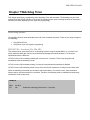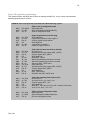
1
CPU-1421
User Manual
MNL-0542-01
revA3
ECO-1994
Effective: 14DEC07
MNL-0542-01 revA3
Disclaimer
Although the information contained herein has been carefully verified, Parvus Corporation assumes no
responsibility for errors that might appear in this document, or for damage to property or persons resulting from
improper use of this manual or related software. Parvus reserves the right to change the contents and form of
this document, as well as the features and specifications of its products at any time without notice. The
information in this publication does not represent a commitment on the part of Parvus. This document contains
proprietary information that is protected by copyright. All rights are reserved. No part of this document may be
photocopied, reproduced, or translated into another language without the prior written consent of Parvus.
Parvus Corporation
3222 S. Washington St.
Salt Lake City, Utah, USA 84115
Phone: +1 (801) 483-1533
Toll-Free:
+1 (800) 483-3152
Main:
+1 (801) 483-1533
Fax:
+1 (801) 483-1523
Email:
Sales:
[email protected]
Support:
[email protected]
Web-site:
http://www.parvus.com
Send us your comments and feedback: [email protected]
Parvus is the U.S. arm of the Eurotech Group (www.eurotech.com), a global family of technology companies
focused on innovative embedded and high performance computing solutions.
Trademarks
Trademarks and registered trademarks appearing in this document are the property of their respective owners.
3
IMPORTANT INFORMATION TO THE USER
Before proceeding further, please carefully read the following paragraphs:
Safety Notices and warnings
FCC information and compliance
This device has been designed to comply with the limits of a Class B digital device pursuant to Part 15 of the
FCC Rules. These limits are designed to provide reasonable protection against harmful interference. The device
generates, uses, and can radiate radio frequency energy and, if not installed and used in accordance with the
instructions, may cause harmful interference to radio communications or to devices that are not appropriately
shielded.
Parvus is not responsible for any radio or device, which may be affected by harmful interference. Appropriate
shielding of susceptible devices is not the responsibility of Parvus. Further, Parvus is not responsible for
unauthorized modifications of Parvus equipment including the substitution or attachment of cables and/or other
unauthorized equipment. If electrical interference is harmfully affecting a device, it is the responsibility of the user
to correct this interference.
In order to minimize the affects of electrical interference, use only shielded data cables with the system.
In accordance with FCC 15.21, changes or modifications not expressly approved by the party responsible for
compliance could void the user’s authority to operate the equipment.
Emissions information for Canada
This Class B digital apparatus complies with Canadian ICES-003. Cet appareil numérique de la classe B est
conforme à la norme NMB-003 du Canada.
CE Marking
This equipment complies with the requirements for CE marking when used in a residential,
commercial, vehicular or light industrial environment.
CPU-1421
MNL-0542-01 revA3
RAEE
The information below is issued in compliance with the regulations as set out by the 2002/96/CE directive,
subsequently superseded by 2003/108/CE, and refers electrical and electronic equipment and the management
of their waste (WEEE). When disposing of a device, including all of its components, subassemblies and
materials that are an integral part of the product, you should take the WEEE directive into consideration.
This symbol has been attached to the equipment or, in the case that this is not possible, on the
packaging, instruction literature and/or the guarantee sheet. By using this symbol it states that the
device has been marketed after August 13th 2005, and implies that you must separate all of its
components when possible, and dispose of them in accordance with local waste disposal legislations.
!
Because of the substances present in the equipment, an improper use or disposal of the refuse can cause
damage to human health and to the environment.
!
With reference to RAEE, it is compulsory to not dispose of the equipment with normal urban refuse,
arrangements should be instigated for separate collection and disposal.
!
For more detailed information about recycling of RAEE, please contact your local waste
collection body.
!
In case of illicit disposal, sanctions will be levied on transgressors.
RoHS
This device, including all it components, subassemblies and the consumable materials that are an integral
part of the product, has been manufactured in compliance with the European directive 2002/95/EC known as
the RoHS directive (Restrictions on the use of certain Hazardous Substances), this directive targets the
reduction of certain hazardous substances previously used in electrical and electronic equipment (EEE).
Anti-static precautions
Always use appropriate antistatic precautions when handing any board. This is to avoid damage
caused by ESD (Electro Static Discharge).
5
Conventions
The following table lists the conventions that are used throughout this manual.
Icon
Notice Type
Information note
Warning
Description
Important features or instructions
Information to alert you to potential
damage to a program, system or device
or potential personal injury
The “Mode” of the register:
R/W Read and write register.
RO Read only register.
W
Meaning of the register when written.
R
Meaning of the register when read.
Hexadecimal numbers:
Hexadecimal numbers are indicated with an “h” suffix (for example: 11Ch).
Other:
NC
Not internally connected
Reserved
Use reserved to Factory
CPU-1421
MNL-0542-01 revA3
Table of Contents
Disclaimer ............................................................................................................................................................ 2
Trademarks .......................................................................................................................................................... 2
IMPORTANT INFORMATION TO THE USER .................................................................................................... 3
Safety Notices and warnings......................................................................................................................... 3
RAEE............................................................................................................................................................. 4
RoHS ............................................................................................................................................................. 4
Anti-static precautions.......................................................................................................................................... 4
Conventions ......................................................................................................................................................... 5
Table of Contents .................................................................................................................................................. 6
Chapter 1
Product Overview ............................................................................................................................ 9
Product Definition............................................................................................................................................... 10
Chapter 2
Jumpers .......................................................................................................................................... 11
Jumper Layout and Configuration...................................................................................................................... 12
Chapter 3
Connectors ..................................................................................................................................... 13
Connector Layout............................................................................................................................................... 14
J1 and J2: the ISA Bus ...................................................................................................................................... 15
The ISA BUS ............................................................................................................................................... 15
J3: PCI Bus ........................................................................................................................................................ 18
How to connect to the CPU other PC/104 & PC/104Plus devices: the stack assembly.................................... 20
J4: Parallel (or FDD), Serial3 and Serial4.......................................................................................................... 21
Parallel/FDD section.................................................................................................................................... 21
Serial ports 3 and 4 section in RS232 Mode............................................................................................... 23
Serial ports 3 and 4 section in RS422 Mode............................................................................................... 23
Serial ports 3 and 4 section in RS485 Mode............................................................................................... 24
J5: Serial 1, Serial 2, Ethernet2, 2 Extra Timers and GPI/O ............................................................................. 25
Timers.......................................................................................................................................................... 26
Watchdog Status ......................................................................................................................................... 26
General Purpose I/O ................................................................................................................................... 26
Ethernet 2 .................................................................................................................................................... 26
J6: Ethernet 1, Keyboard, Speaker, Mouse and Battery ................................................................................... 27
Keyboard Input ............................................................................................................................................ 28
Mouse Input................................................................................................................................................. 28
System reset ............................................................................................................................................... 28
External Battery Input.................................................................................................................................. 28
Speaker Output ........................................................................................................................................... 28
Ethernet 1 .................................................................................................................................................... 28
ACS-9072-00: Multifunction adaptor ........................................................................................................... 29
7
J7: IDE / DOM .................................................................................................................................................... 30
J10: IDE LED ..................................................................................................................................................... 30
J8: Auxiliary Power Connector........................................................................................................................... 31
J11: Slim FDD .................................................................................................................................................... 32
How to connect the FPC floppy cable into the connector ........................................................................... 32
J12: Ethernet 1................................................................................................................................................... 33
Chapter 4 The Setup Program........................................................................................................................ 34
Main menu................................................................................................................................................... 34
Sub menu .................................................................................................................................................... 34
Navigation / Input options............................................................................................................................ 34
Navigation Keys: ................................................................................................................................................ 35
General: ............................................................................................................................................................. 36
Devices: ............................................................................................................................................................. 37
Communications: ............................................................................................................................................... 38
ATAPI Units:....................................................................................................................................................... 39
PCI & ISA ........................................................................................................................................................... 40
Advanced: .......................................................................................................................................................... 41
Error Handling: ................................................................................................................................................... 42
Quit:.................................................................................................................................................................... 43
Chapter 5
BTOOL Program and Solid State Disk......................................................................................... 44
The BTOOL program ......................................................................................................................................... 44
The Integrated Solid State Disk ......................................................................................................................... 47
Chapter 6
Virtual Peripheral ........................................................................................................................... 48
How “Virtual Peripheral” works .......................................................................................................................... 49
Choosing the Virtual Peripheral connection type............................................................................................... 50
Serial Connection: ....................................................................................................................................... 50
Parallel Connection: .................................................................................................................................... 51
The VP2000.EXE program ................................................................................................................................ 52
How to perform a Virtual Peripheral session ..................................................................................................... 53
To perform a Virtual Peripheral session you need:..................................................................................... 53
Follow these steps to perform a Virtual Peripheral session: ....................................................................... 53
Chapter 7
Watchdog Timer............................................................................................................................. 54
Watchdog modes ............................................................................................................................................... 54
BIOS INT 52h - functions 0Ch, 0Dh, 0Eh.................................................................................................... 54
Super I/O registers programming ................................................................................................................ 55
Watchdog time-out pin ....................................................................................................................................... 56
Chapter 8
Troubleshooting............................................................................................................................. 57
Technical/Sales Assistance ............................................................................................................................... 57
CPU-1421
MNL-0542-01 revA3
Returning For Service ........................................................................................................................................ 57
Appendix .............................................................................................................................................................. 58
A.1
Electrical and Environmental Specifications ........................................................................................... 58
Operating Characteristics............................................................................................................................ 58
Absolute Maximum Ratings......................................................................................................................... 59
MTBF........................................................................................................................................................... 59
A.2
Mechanical Dimensions .......................................................................................................................... 60
CPU Dimensions ......................................................................................................................................... 60
LIMITED WARRANTY ....................................................................................................................................... 62
9
Chapter 1 Product Overview
CPU-1421 is a highly integrated PC/104-Plus CPU module, based on the AMD™ Élan™ SC520 133MHz
microprocessor.
Related Products Available:
!
Development kit for CPU-1421
!
TP RJ45 Ethernet adapter
!
2mm to 2.54mm IDE cable
!
Parallel-FDD adapter cable
!
IDE to ATA adapter kit
!
Standard interface cable kit
!
Flat panel adapter kit
For a complete list of our products visit our website: www.parvus.com
CPU-1421
MNL-0542-01 revA3
Product Definition
Architecture:
PC PCI-Architecture with ISA-bus
Dimensions:
Compliant with the PC/104-Plus standard
Processor:
AMD™ Élan™ SC520 133MHz
Memory:
64-128 MB SDRAM soldered onboard
Solid State Disk:
Disk-On-Module, Compact Flash or ATA Flash
Operating System Compatibility:
WinCE®, VxWorks®, Linux® and QNX®
BIOS Flash:
1MB 8bit +5V Flash EPROM
Interfaces:
! IDE controller
! Floppy Disc controller
! Two 10/100Mbit Ethernet controllers
! Four 16C550 compatible serial ports:
- 2 RS-232/485/422, software configurable
- 2 RS-232 fixed
! Parallel port (bi-directional EPP-ECP)
! Two 16-bit user Counter/Timers
! AT keyboard
! PS/2 mouse
Bus:
PCI/ISA PC/104-Plus compliant (ISA-bus with limitations)
Power Supply:
+5V only
11
Chapter 2 Jumpers
This chapter shows the jumper layout and explains how to setup each individual jumper.
CPU-1421
MNL-0542-01 revA3
Jumper Layout and Configuration
Figure 1 shows the jumper layout of the CPU-1421 module. Jumpers are shown as JP followed by the jumper's
number, a red square pad indicates pin 1 of the 3-pin jumper.
JP3
JP1
JP2
Figure 1.
Jumpers and solder jumpers
Table 1.
PIN
JP1
Type
2 pin
Function
External Bios
JP2
2 pin
Invalid Setup
JP3
JP4
JP5
2 pin
2 pin
3 pin
Module Reset
Reserved
Ethernet Controller
Jumper Functions
Settings
Open: Module starts with internal BIOS
Closed: Module starts with External Bios
Open: Module starts with saved parameters
Closed: Module starts with default settings
When these two pins are shorted the system will reset
1-2: Ethernet 1 Disabled
2-3: Ethernet 2 Disabled
Open: Ethernet1 and Ethernet2 Enabled
Default
Open
Open
Open
Open
Open
13
Chapter 3 Connectors
This chapter provides a brief description of each connector found on the CPU-1421, with their position and
function.
CPU-1421
MNL-0542-01 revA3
Connector Layout
Figure 2 shows the connector layout on the CPU-1421 along with their function. Connectors are shown as J
followed by its designated number: a red square pad indicates pin 1 of each connector.
J5
J4
J11
J3
J1 J2
J12
J8
Figure 2.
Connector #
J1
J2
J3
J4
J5
J6
J7
J8
J9
J10
J11
J12
Connector layout
Function
ISA Bus
ISA Bus
PCI Bus
Parallel, Serial3 and Serial4
Serial1, Serial2, Timer, Watchdog
Status, GPI/O and Ethernet2
Ethernet 1, Keyboard, Mouse,
Speaker and Battery
IDE / DOM
Auxiliary power supply input
Reserved
IDE Led
Floppy Disk
Ethernet 1
Table 2.
Qty of pins
64
40
120
40
Format
Pitch (mm)
PC104: 32x2
2.54
PC104: 20x2
2.54
PC104PLUS: 30x4
2.00
Hirose DF13 20x2
1.25
40
Hirose DF13 20x2
1.25
26
Pin strip 13x2
2.00
44
12
14
2
26
8
Pin strip 22x2
Pin strip 6x2
Pin strip 7x2
Pin strip 2x1
ZIF 26
SIL 8
2.00
2.54
2.00
2.00
1.00
2.00
Connector Functions
15
J1 and J2: the ISA Bus
The ISA BUS
Connectors J1 and J2 carry the signals for the ISA Bus.
These signals match definitions of the IEEE P996 standard.
Below is shown a picture of the ISA BUS
J1
J2
Figure 3.
ISA BUS layout
According to the PC/104 specifications, these connectors include KEY pins; these are filled holes in the upper
side and missing pins in the lower side of the bus. This is done to avoid the wrong insertion in/of another
module.
Unsupported ISA Bus Functions
The following ISA bus features are not supported.
"
Because the CPU itself does not support address pipelining, address pipelining is not supported on the
ISA bus.
"
External master access is not supported, and the CPU is always the master on the ISA bus (external
masters can be accommodated by the PCI bus).
"
“GPIOCS16” and “GPMEMCS16” do not cause the ISA bus timings to change for the bus cycles during
which these signals are asserted.
"
“IOCHRDY” is supported only as an input for the slave devices that require wait states. Since there is no
external master support, “IOCHRDY” is not supported as an output.
"
“IOCHK” is not supported.
"
The REFRESH pin is not supported.
"
“NOWS” is not supported.
"
IRQ15 is not supported. By customer request, a special setting can be made to support IRQ15;
however, that would make IRQ9 unavailable. The factory can only perform this special setting.
"
The ISA bus interface timing is configured to support most ISA bus devices. However, the CPU-1421’s
ISA bus does not support all legacy ISA timing.
CPU-1421
MNL-0542-01 revA3
Pin #
1
2
3
4
5
6
7
8
9
10
11
12
13
14
15
16
17
18
19
20
21
22
23
24
25
26
27
28
29
30
31
32
Use
ISA Bus
ISA Bus
ISA Bus
ISA Bus
ISA Bus
ISA Bus
ISA Bus
ISA Bus
ISA Bus
ISA Bus
ISA Bus
ISA Bus
ISA Bus
ISA Bus
ISA Bus
ISA Bus
ISA Bus
ISA Bus
ISA Bus
Not Connected
ISA Bus
ISA Bus
ISA Bus
ISA Bus
ISA Bus
ISA Bus
ISA Bus
ISA Bus
ISA Bus
ISA Bus
ISA Bus
ISA Bus
Signal
IOCHK#
Ground
D7
RSTDRV
D6
+5 Volts
D5
IRQ 9
D4
-5 Volts
D3
DRQ2
D2
-12 Volts
D1
ZEROWS#
D0
+12 Volts
IOCHRDY
Key
AEN
SMEMW#
A19
SMEMR#
A18
IOW#
A17
IOR#
A16
DACK3#
A15
DRQ3
Table 3.
Pin #
Use
ISA Bus
33
ISA Bus
34
ISA Bus
35
ISA Bus
36
ISA Bus
37
ISA Bus
38
ISA Bus
39
ISA Bus
40
ISA Bus
41
ISA Bus
42
ISA Bus
43
ISA Bus
44
ISA Bus
45
ISA Bus
46
ISA Bus
47
ISA Bus
48
ISA Bus
49
ISA Bus
50
ISA Bus
51
ISA Bus
52
ISA Bus
53
ISA Bus
54
ISA Bus
55
ISA Bus
56
ISA Bus
57
ISA Bus
58
ISA Bus
59
ISA Bus
60
ISA Bus
61
ISA Bus
62
ISA Bus
63
ISA Bus
64
J1 pinout
Signal
A14
DACK1#
A13
DRQ1
A12
REFRESH#
A11
ISACLK
A10
IRQ 7
A9
IRQ 6
A8
IRQ 5
A7
IRQ 4
A6
IRQ 3
A5
DACK2#
A4
TC
A3
BALE
A2
+5 Volts –1
A1
OSC
A0
Ground 1
Ground 3
Ground 2
17
Pin #
1
2
3
4
5
6
7
8
9
10
11
12
13
14
15
16
17
18
19
20
CPU-1421
Use
ISA Bus
ISA Bus
ISA Bus
ISA Bus
ISA Bus
ISA Bus
ISA Bus
ISA Bus
ISA Bus
ISA Bus
ISA Bus
ISA Bus
ISA Bus
ISA Bus
ISA Bus
ISA Bus
ISA Bus
ISA Bus
ISA Bus
ISA Bus
Signal
Ground 0
Ground 1
SBHE#
ISA_MEMCS16#
LA23
IOC16#
LA22
IRQ10
LA21
IRQ11
LA20
IRQ12
LS19
IRQ15
LA18
IRQ14
LA17
DACK0#
MEMR#
DRQ0
Table 4.
Pin #
Use
ISA Bus
21
ISA Bus
22
ISA Bus
23
ISA Bus
24
ISA Bus
25
ISA Bus
26
ISA Bus
27
ISA Bus
28
ISA Bus
29
ISA Bus
30
ISA Bus
31
ISA Bus
32
ISA Bus
33
ISA Bus
34
ISA Bus
35
ISA Bus
36
ISA Bus
37
ISA Bus
38
ISA Bus
39
ISA Bus
40
J2 pinout
Signal
MEMW#
DACK5#
SD8
DRQ5
SD9
DACK6#
SD10
DRQ6
SD11
DACK7#
SD12
DRQ7
SD13
+5 Volts
SD14
MASTER#
SD15
Ground 2
Not Connected
Ground 3
MNL-0542-01 revA3
J3: PCI Bus
Connector J3 carries signals of the PCI Bus. The PCI Bus mechanical interface is a stackable 30x4 header. This
interface carries all of the required PCI signals per PCI Local Bus Specification Version. 2.1.
Below is shown a picture of the PCI BUS.
J3
PCI Bus
Figure 4.
PCI BUS layout
Unsupported PCI Bus Functions
The following list summarizes some of the PCI bus functionality that is not supported in the CPU1421’s PCI host bridge. These functions are listed as optional in the PCI bus specification.
"
66MHz is not supported.
"
64-bit data is not supported.
"
64-bit addressing (dual address cycles) is not supported due to the maximum 32-bit address space of
the Am5x86 CPU.
"
Cacheable PCI bus memory (SBDONE, SBO) is not supported.
"
The optional “CLKRUN” pin is not supported.#
"
The “LOCK” pin is an optional pin not required in most systems, because other mechanisms are typically
employed for coherency.
"
Address/data stepping is not supported as a master due to the performance implications.
"
The CPU does not support a downstream “Southbridge” device, because most peripherals normally
included in a Southbridge are integrated into the CPU.
"
The optional message-signaled interrupt feature described in the PCI Local Bus Specification, Revision
2.2, is not supported in the CPU-1421.
Unsupported PCI Bus Configuration Registers
Some standard PCI bus configuration registers are not implemented, because the CPU is a host-toPCI bridge and does not support some optional PCI functionality.
"
Base Address registers are not implemented, because the CPU is the host PCI device. Target address
space configuration is done through CPU-specific configuration.
"
“Latency timer” and “MAX_LAT”, “MIN_GNT” are not implemented, because the CPU’s PCI host bridge
does not support multiple data phase transactions as a master.
"
Cache line size is not implemented, because the CPU PCI host bridge does not support cacheable PCI
memory.
For further info about ISA bus and PCI bus please refer to www.pc104.org
19
Pin
1
2
3
4
5
6
7
8
9
10
11
12
13
14
15
16
17
18
19
20
21
22
23
24
25
26
27
28
29
30
A
GND
VI/O
AD05
C/BE0#
GND
AD11
AD14
+3.3V
SERR#
GND
STOP#
+3.3V
FRAME#
GND
AD18
AD21
+3.3V
IDSEL0
AD24
GND
AD29
+5V
REQ0#
GND
GNT1#
+5V
CLK2
GND
+12V
-12V
B
Reserved
AD02
GND
AD07
AD09
VI/O
AD13
C/BE1#
GND
PERR#
+3.3V
TRDY#
GND
AD16
+3.3V
AD20
AD23
GND
C/BE3#
AD26
+5V
AD30
GND
REQ2#
VI/O
CLK0
+5V
INTD#
INTA#
REQ3#
Table 5.
CPU-1421
C
+5
AD01
AD04
GND
AD08
AD10
GND
AD15
Reserved
+3.3V
LOCK#
GND
IRDY#
+3.3V
AD17
GND
AD22
IDSEL1
VI/O
AD25
AD28
GND
REQ1#
+5V
GNT2#
GND
CLK3
+5V
INTB#
GNT3#
J3 pinout
D
AD00
+5V
AD03
AD06
GND
M66EN
AD12
+3.3V
PAR
Reserved
GND
DEVSEL#
+3.3V
C/BE2#
GND
AD19
+3.3V
IDSEL2
IDSEL3
GND
AD27
AD31
VI/O
GNT0#
GND
CLK1
GND
RST#
INTC#
GND
MNL-0542-01 revA3
How to connect to the CPU other PC/104 & PC/104Plus devices: the stack
assembly
The ISA Bus connectors of the module are designed to allow the connection onto a stack of other PC/104 and/or
PC/104Plus devices.
We recommend you to follow the procedure below ensuring that stacking of the modules does not damage
connectors or electronics parts.
1. Turn off power to the PC/104Plus system or stack.
2. Select and install standoffs to properly position the module on the PC/104Plus stack.
3. Touch a grounded metal part of the rack to discharge any build up of static electricity.
4. Remove the module from its anti-static bag.
5. Check that keying pins in the bus connector are properly positioned.
6. Check the stacking order; make sure an XT bus card will not be placed between two AT bus cards or it will
interrupt the bus’s signals.
7. Hold the module by its edges and orient it so that the bus connector pins line up with the matching connector
on the stack.
8. Press evenly the module onto the PC/104Plus stack.
The picture below shows a typical module stack with two PC/104Plus modules, one PC/104 16-BIT module, and
one PC/104 8-BIT module.
The maximum configuration for the PCI bus of PC/104Plus modules is four plus the Host Board. If standard
PC/104 modules are used in the stack, they must be the top module(s) because they will normally not include
the PCI bus.
Stackthrough
8-bit module
0.435 in. (11 mm)
0.6 in. (15mm) Spacers (4 plcs.)
0.6 in. (15 mm)
Stackthrough
16-bit module
0.6 in. (15mm) Spacers (4 plcs.)
Stackthrough
PC/104Plus module
0.100 in. (2.54 mm)
0.6 in. (15mm) Spacers (4 plcs.)
0.062 in. (1.57 mm)
Non-Stackthrough
PC/104Plus module
Figure 5.
The Module Stack
Do not force the module onto the stack! Wiggling the module or applying too much pressure may
damage it. If the module does not readily press into place, remove it, check for bent pins or out-ofplace keying pins, and try again.
21
J4: Parallel (or FDD), Serial3 and Serial4
J4 implements the following functions:
!
Parallel/FDD port
!
Serial ports 3 and 4; these ports are RS232, RS422 or RS485 selectable
Figure 6.
J4 Connector Layout
Parallel/FDD section
The user can choose the Parallel port or the FDD setting using the Setup Program.
Pin #
1
3
5
7
9
11
13
15
17
19
21
Signal
STROBE#
PD0
PD1
PD2
PD3
PD4
PD5
PD6
PD7
ACK#
BUSY
Pin #
2
4
6
8
10
12
14
16
18
20
22
Signal
PE
SLCT
GND1_LPT
AUTOFD#
GND2_LPT
ERROR#
GND3_LPT
INIT#
GND4_LPT
SLCTIN#
Not Connected
The symbol “#” stands for active low
In order to simplify the connection between the parallel port and a floppy disk drive Parvus makes available a
Floppy disc drive adaptor: the ACS-6000.
CPU-1421
MNL-0542-01 revA3
HOW TO USE THE PARVUS/EUROTECH ACS-6000 FDD ADAPTOR
There are two configurations available in the Parvus FDD Adaptor:
! Female configuration
! Male configuration
Connector
J1A
J1
J2
J3
Use
Male configuration
Female configuration
Power supply (5V) used by the adaptor
Parallel Port Flat Cable Connector
Notes
For connecting to a Floppy Disk Flat Cable
For direct connection to a Floppy Disk Drive
This is NOT for powering the Floppy Disc Drive
To the FDD Cable/Connector
Female Config.
Male Config.
Power Supply
GND PIN1
+5V PIN2
To the Parallel Port
Figure 7.
The ACS-6000 Adaptor layout
WARNING! TO AVOID MALFUNCTIONS, BE CAREFUL TO CONNECT THE FLOPPY DRIVE CABLE
IN THE FOLLOWING WAY:
Commonly found Floppy Drive cables are structured as shown in the following picture. With this type of
cable, only the second connector can be connected to the Parvus Floppy Disk Drive Adaptor. The “FDD
connector” end of the cable is connected to the rear connector of the Floppy Drive.
To FDD
adapter
To FDD
connector
X
Figure 8.
Floppy Drive Cable.
23
Serial ports 3 and 4 section in RS232 Mode
Pin #
23
24
25
26
27
28
29
30
31
32
33
34
35
36
37
38
39
40
Port
COM3
COM3
COM3
COM3
COM3
COM3
COM3
COM3
COM3
COM4
COM4
COM4
COM4
COM4
COM4
COM4
COM4
COM4
Signal
DCD
DSR
RX
RTS
TX
CTS
DTR
RI
GND
GND
DCD
DSR
RX
RTS
TX
CTS
DTR
RI
Function
Data Carrier Detect
Data Set Ready
Receive Data
Request To Send
Transmit data
Clear To Send
Data Terminal Ready
Ring Indicator
Signal Ground
Signal Ground
Data Carrier Detect
Data Set Ready
Receive Data
Request To Send
Transmit data
Clear To Send
Data Terminal Ready
Ring Indicator
Serial ports 3 and 4 section in RS422 Mode
Pin #
23
25
27
29
31
32
33
35
37
39
Port
COM3
COM3
COM3
COM3
COM3
COM4
COM4
COM4
COM4
COM4
Signal
-TX
+TX
-RX
+RX
GND
GND
-TX
+TX
-RX
+RX
Function
Transmit data
Transmit Data
Receive Data
Receive Data
Signal ground
Signal ground
Transmit data
Transmit Data
Receive Data
Receive Data
In/out
Out
Out
In
In
--Out
Out
In
In
Pins not shown in the table are not connected
CPU-1421
MNL-0542-01 revA3
Serial ports 3 and 4 section in RS485 Mode
Pin #
23
25
31
32
33
35
Port
COM3
COM3
COM3
COM4
COM4
COM4
Signal
-TX/-RX
+TX/+RX
GND
GND
-TX/-RX
+TX/+RX
Function
Transmit/Receive data
Transmit/Receive data
Signal ground
Signal ground
Transmit/Receive data
Transmit/Receive data
In / Out
In / Out
In / Out
--In / Out
In / Out
Pins not shown in the table are not connected
Note. When the Serial ports are used in RS485 mode, the bi-directional line must be controlled
via software using the Data Terminal Ready (DTR) signal of the serial controller. This signal is
defined by bit 0 of the UART Modem Control Register (MCR) and the bi-directional line is
controlled as follows:
" Bit 0 of the MCR register = 0 means RS485 line receiving
" Bit 0 of the MCR register = 1 means RS485 line transmitting
The I/O address of the MCR is "Serial port Base address"+4H.
25
J5: Serial 1, Serial 2, Ethernet2, 2 Extra Timers and GPI/O
J5 implements the following functions:
!
Serial1 and Serial 2 (RS232 only)
!
2 Extra Timers
!
Watchdog Status
!
General Purpose I/O
!
Ethernet 2
J5
Figure 9.
J5 Connector Layout
Pin #
1
2
3
Function
Timer 0
Timer 0
Timer 1
Signal
TMRIN0 IRQ8#
TMROUT0
TMRIN1
Pin #
21
22
23
Function
Not Connected
Not Connected
Serial 1
4
Timer 1
TMROUT1
24
Serial 1
5
Watchdog Status
WDTL
25
Serial 1
6
Watchdog Status
GND1
26
Serial 1
7
GPI/O
GPI/O14
27
Serial 1
8
GPI/O
GPI/O15
28
Serial 1
9
GPI/O
GPI/O13
29
Serial 1
10
GPI/O
GND
30
Serial 1
11
Ethernet 2
LINK_B
31
Serial 1
12
Ethernet 2
ACTIVITY_B
32
Serial 2
13
Ethernet 2
TXOUT2+
33
Serial 2
14
Ethernet 2
TXOUT2-
34
Serial 2
15
Ethernet 2
RXIN2+
35
Serial 2
16
Ethernet 2
RXIN2-
36
Serial 2
17
Ethernet 2
VCC3
37
Serial 2
18
Ethernet 2
GND
38
Serial 2
19
--
Not Connected
39
Serial 2
20
--
Not Connected
40
Serial 2
The symbol “#” stands for active low
Table 6.
CPU-1421
J5 connector pin-out
Signal
GND
GND
DCD1
DSR1
RX1
RTS1
TX1
CTS1
DTR1
RI1
GND
GND
DCD2
DSR2
RX2
RTS2
TX2
CTS2
DTR2
RI2
MNL-0542-01 revA3
Timers
Two 16-bit Extra Timers are provided with this CPU. These extra timers are intended for most generic timing or
counting applications, such as generating periodic interrupts and measuring or counting external events.
Other features included are:
!
Clock source from the system clock. The maximum clock is 33MHz/4
!
One interrupt output for each timer
!
Several modes of operation:
"
Interrupt on terminal count
"
Hardware re-trigger mode
"
Rate and square wave generation
"
Continuous mode
Watchdog Status
It is possible to connect a device to view the watchdog status using these two pins.
For further information, refer to Chapter 7
General Purpose I/O
The CPU 1421 supports three independently programmable Input/Output signals (GPIO), these can be used to
monitor signals or control external devices.
The GPIO signals can be programmed for the following functions:
"
Read as inputs (default configuration, after the reset)
"
Driven High or Low as outputs
Ethernet 2
To establish an Ethernet connection you must use the Parvus/Eurotech ACS-9095 Ethernet Adapter, it must be
connected between the CPU-1421 J5 connector and the RJ45 network cable.
Network drivers
The Ethernet is based on the Realtek RTL8139C chipset and is supported by most operating systems.
27
J6: Ethernet 1, Keyboard, Speaker, Mouse and Battery
J6 implements the following functions:
!
AT Keyboard
!
PS/2 Mouse
!
System reset
!
External battery
!
Speaker
!
Power button
!
Ethernet 1
Figure 10. J6 Connector layout
Pin #
1
2
3
4
5
6
7
8
9
10
11
12
13
Function
Generic
Generic
Keyboard
Keyboard
Mouse
Mouse
Battery
Speaker
Reset (push-button)
Not Connected
Not Connected
Not Connected
Not Connected
Signal
GND
VDD
KBDATA
KBCLK
MSDAT
MSCLK
BAT_IN
SPKR
RES_PB_IN
-----
Table 7.
CPU-1421
Pin #
14
15
16
17
18
19
20
21
22
23
24
25
26
Function
Not Connected
Not Connected
Not Connected
Not Connected
Not Connected
---------
J6 Connector pinout
Signal
LINK_A
ACTIVITY_A
TXOUT1+
TXOUT1RXIN+
RXINVCC3
GND
MNL-0542-01 revA3
Keyboard Input
An AT compatible keyboard can be connected to the module through connector J6.
Mouse Input
A PS/2 compatible mouse can be connected to the J6 connector
System reset
By connecting pin 9 and ground will perform a hardware reset of the module. We advise using an external pushbutton, normally open.
External Battery Input
Pin 7 of the multifunction connector allows for the connection of an external backup battery.
This battery is used when the module is powered down to preserve the date & time in the Real Time Clock.
Speaker Output
A transistor supplying 0.1W of power to an external speaker controls these outputs. A transistor amplifier buffers
the speaker signal. Use a small general-purpose 2” or 3” inch permanent magnet speaker with an 8-Ohm voice
coil.
The audio output is based on two signals: the output of Timer 2, and the programming of two bits, 0 and 1, at I/O
port 61h. Bit 1 of I/O port 61h is one term of a 2-input AND gate. The other term is the output from Timer 2.
Thus, setting bit 1 to logic 1 enables the output of Timer 2 to the speaker, and logic 0 disables it. Disabling Timer
2 by setting bit 0 of port 61h to a 0 causes its output to go high. Then you can use bit 1 of port 61h to control the
speaker directly.
Ethernet 1
To establish an Ethernet connection you must use the Parvus ACS-9071 Ethernet Adapter, it must be connected
between the CPU-1421 J6 connector and the RJ45 network cable.
NOTE: The Ethernet 1 port is also made available on connector J12. The user must choose
either J6 or J12 (not both) in order to use this peripheral
Network drivers
The Ethernet is based on the Realtek RTL8139C chipset and is supported by most operating systems.
29
ACS-9072-00: Multifunction adaptor
Figure 11.
Component Label
Location
Description
Pins
Format
Pitch (mm)
BT1
LS1
D1
D3
S1
J1
J2
J3
J4
J5
J6
Bottom
Bottom
Top
Top
Top
Bottom
Top
Top
Bottom
Bottom
Bottom
Battery, 3.6V, 60mAh
Speaker,
LED (Green), Power
LED (Yellow), Speaker
Reset Button
Extension Keyboard
Keyboard Input
Mouse Input
Multifunction Output
Not Used with this CPU
Mouse Output
4
6
6
10
2
4
4x1
Mini DIN
Mini DIN
5x2
2x1
4x1
2.54
2.54
2.54
2.54
Connector
J1
Description
Ext. Keyboard Input
J2
Keyboard Input
J3
Mouse Input
CPU-1421
ACS-9072-00 Top / Bottom View
Pin #
1
2
3
4
1
2
3
4
5
6
1
2
3
4
5
6
Signal
VCC
KB Clock
Ground
KB Data
KB Data
NC
Ground
VCC
KB Clock
NC
Mouse Data
NC
Ground
VCC
Mouse Clock
NC
Connector
J4
Description
Multifunction Output
To CPU J6
J6
Mouse output
Pin #
1
2
3
4
5
6
7
8
9
10
1
2
3
4
Signal
SPKR
NC
RES_PB_IN
NC
KBDAT
KBCLK
GND
+5V
BATT_IN
NC
VCC
Mouse Clock
Ground
Mouse Data
MNL-0542-01 revA3
J7: IDE / DOM
J7 provides an interface for one or two Integrated Device Electronics (IDE) hard disk drives.
Figure 12. J7and J10 Connector layout
To install the hard disk, perform the following operations:
!
Hardware installation.
Connect the hard disk to the module using a data cable, and then connect the hard disk to the power
supply according to the device’s specifications. Make sure that pin 1 of the IDE connector and pin 1 of
the drive or drives are correctly connected. Pin 1 of the interface cable is usually indicated by a stripe
along the edge of the cable. If two hard disks need to be connected, they must be configured for
common operation (i.e. master/slave or cable select connection).
!
IDE BIOS Setup.
The hard disk parameters can be configured using the Setup program. If the hard disk is connected to
the module without set-up configuration or with a wrong set-up configuration, a time-out for a few
minutes occurs, then the boot is performed from the floppy disk.
!
Software initialization for specific operating systems.
Refer to the OS documentation.
J10: IDE LED
It is possible to connect an LED to the J10 connector that displays the IDE activity.
Pin
1
2
Signal
Function
IDE Led anode
IDE Led anode
IDE Led cathode
IDE Led cathode
Table 8.
J10 pinout
31
J8: Auxiliary Power Connector
One auxiliary power connector is available on the CPU-1421 module; this can be used to power the module as
an alternative to the PC/104Plus bus.
J8
Figure 13. J8 Connector layout
Pin
1
2
3
4
5
6
Signal
GND
VDD (+5VDC)
Not Connected
+12VDC
-5VSB
-12VDC
Table 9.
Pin
7
8
9
10
11
12
Signal
GND
VDD (+5VDC)
GND
Not Connected
Not Connected
Not Connected
J11 pinout
The number and position of the pins that have to be connected depends on the Power Supply model. Refer to
the following to ensure the correct connections.
AT Power Supply
!
Connect pin 1 and 7 to the ground signal of the AT Power Supply Unit.
!
Connect pin 2 and 8 to the +5VDC source on the AT Power Supply Unit.
!
Connect pin 4 to the +12VDC and pin 6 to the –12VDC sources on the AT Power Supply Unit only
if requested by other boards connected to the PC/104Plus ISA bus (see the following note).
ATX Power Supply
!
Connect pin 1 and pin 7 to the ground signal of the ATX Power Supply Unit.
!
Connect pin 2 and pin 8 to the +5VDC source on the ATX Power Supply Unit.
!
Connect pin 4 to the +12VDC and pin 6 to the –12VDC sources on the ATX Power Supply Unit
only if requested by other boards connected to the PC/104Plus ISA bus (see the following note).
Power button
If the soft power management is enabled, a low signal in this pin turns the system on or off.
Note. The +12VDC and -12VDC voltages are neither used nor generated by the CPU-1421 module:
they are only conveyed on the PC/104Plus bus (connector J1) and can be used by other devices or
modules that are stacked onto the CPU module.
WARNING! IMPROPER CONNECTION OF THE POWER SUPPLY, WILL RESULT IN SERIOUS
DAMAGE TO THE MODULE.
CPU-1421
MNL-0542-01 revA3
J11: Slim FDD
This connector can only be used to connect a Slim FDD, and it is composed of two parts, The upper part (the
Actuator) and the lower part (the Receptacle).
ACTUATOR
RECEPTACLE
J11
Figure 14.
J11 Connector layout
The connection between the FDD and the module is established by using a Flat Printed Circuit (FPC) cable, the
floppy controller must be enabled in the set-up program before the FDD can be used, and also only one FDD
can be used.
How to connect the FPC floppy cable into the connector
Step 1:
1
Lift up the actuator
Step 2:
FPC
cable
2
Insert the Flat Printed Circuit cable so that the copper tracks face the PC/104 connector. The FPC connector has
contact pins on one side only. The same is true for the connector on the FDD (please refer to the FDD manual
for further info). If incorrectly connected, the FDD will not function.
Step 3:
OK
3
Push down the actuator locking the cable firmly.
Note: Reverse the procedure above to remove the FDD
33
J12: Ethernet 1
J12 implements a second connection for the Ethernet 1 port.
NOTE: The Ethernet 1 port is also made available on connector J6. The user must choose
either J6 or J12 (not both) in order to use this peripheral
To establish an Ethernet connection you must use the Parvus Ethernet Adapter; it must be connected between
the CPU-1421 J12 connector and the RJ45 network cable.
J12
Figure 15.
J12 Connector layout
Network drivers
The Ethernet is based on the Realtek RTL8139C chipset and is supported by most operating systems.
Pin #
1
2
3
4
5
6
7
8
Function
Transmission Data Transmission Data +
Ground
Link LED
Receive Data Receive Data +
Activity LED
+3.3V
Table 10.
CPU-1421
Signal
TXOUT1TXOUT1+
GND
LED1_1
RXIN1RXIN1+
LED0_1
VCC3
J12 pinout
MNL-0542-01 revA3
Chapter 4 The Setup Program
Note: This Section refers to BIOS version 4_36_05, Other version may differ.
Main Menu
Sub Menu
Navigation /
Input Options
As you can see from the diagram above the display is separated into 3 zones:
Main menu
To the left is the Main menu; this shows a list of possible Sub menus that can be selected.
Sub menu
The right hand panel will change depending on the selected Tab in the Main menu.
Navigation / Input options
In the Lower right hand corner icons are displayed that show all the possible actions that you can perform with
the selected Parameter or Tab.
35
Navigation Keys:
In the lower right hand corner of the BIOS Setup screen, you will notice a selection of icons, these show what
keys can be used with the currently selected item, and they are as follows:
Icon
CPU-1421
Keys
Use
!
Up Arrow
!
Go to the next field above
!
Down Arrow
!
Go to the next field below
!
Left Arrow
!
Go to the next field to the right
!
Right Arrow
!
Go to the next field to the Left
!
!
Enter
Return
!
!
!
Select field to modify
Select an option i.e. “Detect Now”
Accept a value you have entered
!
Escape
!
!
Cancel a value you are entering
Go back to the Main menu
!
!
Page Down
+
!
Select next option in a list
!
!
Page Up
-
!
Select previous option from a list
!
Numbers 0 to 9
!
Enter a numerical number using 0 to 9
!
Backspace
!
Erase last character entered
MNL-0542-01 revA3
General:
Option
Time
Date
Floppy Disc 1
Floppy Disc 2
Floppy Disc 3
Floppy Disc 4
Keyboard
Quick Boot
Boot Try Sequence
Sub Option
Hours
Minutes
Seconds
Month
Day
Year
Possible selections
! 00 ~ 23
! 00 ~ 59
! 00 ~ 59
! Jan ~ Dec
! 01 ~ 31
! 2006 ~ 2999
! None
! 360 KB
! 1.2 MB
! 720 KB
! 1.44 MB
! Integrated SSD
! Not Present
! Present
! Disabled
! Enabled
! FD1 / HD1 / NET
! NET / FD1 / HD1
! HD1 / FD1 / NET
! CD-ROM / FD1 / HD1
Notes:
Floppy Disc X:
!
Drive letters are assigned consecutively starting from A:
!
We suggest that it is good practice to use Floppy Disc 1 before using Floppy Disc 2 etc.
!
The Integrated SSD is a read only device.
Quick Boot:
!
Quick Boot will take less than 5 Seconds, this is done by skipping the following tests:
!
System memory pattern test
!
Keyboard detection
!
Floppy disk presence (seek test)
!
RTC time test.
37
Devices:
Option
Floppy Controller
EIDE Port
Video Controller
Network Adapter 1
Network Adapter 2
PS/2 Mouse
CPU-1421
!
Enable
!
IRQ
Possible selections
! Disabled
! Enabled on J4 (Parallel port)
! Enabled on J11
! Disabled
! Enabled
! Replace with Add-On if any
! Always use Integrated
! Disabled
! Enabled
! Enabled + Boot Firmware
! Disabled
! Enabled
! List of available IRQ numbers
MNL-0542-01 revA3
Communications:
Option
Serial Port 1 (J5)
Serial Port 2 (J5)
Serial Port 3 (J4)
Serial Port 4 (J4)
Sub Option
Address
Mode
VP2000 / VT100
IRQ
Parallel Port (J4)
Address
Mode
VP2000
IRQ
DMA
Possible selections
! Disabled (All Ports)
! 3F8h (Ports 1, 3 & 4)
! 2F8h (Ports 2, 3 & 4)
! 3E8h (Ports 3 & 4)
! 2E8h (Ports 3 & 4)
! RS232 (Ports 1, 2, 3 & 4)
! RS422 (Ports 3 & 4)
! RS485 (Ports 3 & 4)
! Yes
! No
! None
! List of available IRQ numbers
! Disabled
! 0378h
! 0278h
! Printer
! Bidirectional
! EPP-1.9 and SPP
! EPP-1.7 and SPP
! ECP
! ECP and EPP-1.9
! ECP and EPP-1.7
! Yes
! No
! None
! List of available IRQ numbers
! None
! 0
39
ATAPI Units:
Option
Master 1
Slave 1
Sub Option
Mode
Trans.
Size (MB)
Cyls
Heads
Sec/Tr
Detect Now
CPU-1421
Possible selections
! None
! Auto
! LBA
! CHS
! CD-ROM
! Other
! PIO-0
! PIO-1
! PIO-2
! PIO-3
! PIO-4
! LBA
! ECHS
! Automatically calculated using
Cyls, Heads & Sec/Tr
! 0 ~ 65536
! 0 ~ 64
! 0 ~ 255
! Selection will attempt to Auto-detect
any devices connected.
Notes
!
!
!
!
!
!
!
3.3 MBps Transfer Rate
5.2 MBps Transfer Rate
8.3 MBps Transfer Rate
11.1 MBps Transfer Rate
16.6 MBps Transfer Rate
LBA Translation
Extended CHS translation
!
!
!
Cylinders
Heads
Sectors per track
MNL-0542-01 revA3
PCI & ISA
Option
Memory at 0C8000h. 0CFFFFh
Memory at 0D0000h. 0D7FFFh
Memory at 0D8000h. 0DFFFFh
ISA Irq for PCI INT_A (Share 2)
ISA Irq for PCI INT_B (Share 2)
ISA Irq for PCI INT_C (Share 2)
ISA Irq for PCI INT_D (Share 2)
Bus Mater (Devices)
Latency Time (Devices)
Possible selections
!
!
Reserved for PCI
Available on ISA
!
List of available IRQ numbers
!
!
!
Disabled
Enabled
0 ~ 255
41
Advanced:
Option
Legacy PnP Support
CPU Clock Speed
L1 Cache Mode
Watch Dog start at boot
Watch Dog Timeout (>=2)
Possible selections
! Disabled
! Enabled
! 100 MHz
! 133 MHz
! Write Back
! Write Through
! Disabled
! Seconds
! Minutes
! 2 ~ 255
Note:
Watch Dog Timeout can be set to between 2 & 255 seconds or 2 & 255 minutes,
as defined by Watch Dog start at boot parameter.
CPU-1421
MNL-0542-01 revA3
Error Handling:
Option
Error on Keyboard
Error on Video
Error on Floppy Disc
Error on Fixed Disc
Error on Real Time Clock
Possible selections
!
!
Ignore
Prompt User
43
Quit:
Pressing the Enter or Return keys when Quit is selected the following will be displayed:
Option
Save data to EEPROM
Discard Changes
Notes
The configuration data will be saved to the EEPROM
The Module will then reboot
Changes made will be discarded
The Module will reboot with the original settings
Note: When quit has been selected, it is not possible to return to the configuration pages, you must reboot the
system and re-enter the BIOS using F2 during the initial boot sequence
CPU-1421
MNL-0542-01 revA3
Chapter 5 BTOOL Program and Solid State Disk
This chapter explains how to use the BTOOL Program and gives information about the Integrated Solid State
Disk.
Warning: The BTOOL Program can be different for each CPU and each BIOS version. For the latest
version visit the site: www.parvus.com
When you download a new BIOS revision you should also find the latest copy of BTOOL enclosed
in the package, this will be the correct version to use with the BIOS, it should not be used with
other revisions (older or newer).
The BTOOL program
BTOOL is a utility used to update the BIOS Flash EPROM; it can be used for the following tasks:
!
Upgrading the BIOS
!
Installation of a MiniDOS compatible program into the Flash (Integrated SSD)
!
Installing a BIOS Extension onto the flash device
PLEASE NOTE:
The BTOOL program should only be run in the MS-DOS environment, not a DOS WINDOW, we advise
the creation of a bootable MS-DOS floppy disc.
The following precautions should be taken into consideration:
!
!
!
!
Power assured during all the program executions.
AUTOEXEC.BAT and CONFIG.SYS should not have any parameters
No memory manager should be loaded.
HIMEM or EMM386 will cause errors with BTOOL
The program is run at the command line by typing BTOOL (or BTOOL.EXE) followed by an appropriate
argument, as described in the following pages.
45
If no arguments are used the following on-line help page will be displayed:
Argument
/S
/L
/U
/G [Filename]
/P [Filename]
/B [Filename]
/V [Filename]
/E [Filename]
/DA
/DB
Definition
Run the Setup program without needing to reboot the
system.
Lock the Setup Program.
Unlock the Setup Program.
Gets the Setup Data from the system and save it in a file
with the name [FILENAME.BIN].
This option takes Setup data from the file [FILENAME.BIN]
and stores it to the Flash EPROM.
This option updates the entire BIOS firmware with the
version stored in the file named [FILENAME.BIN]
This option updates only the video BIOS firmware with the
new version stored in the file named [FILENAME.BIN]
This option updates the Emergency BIOS Firmware with
the new version stored in the file [FILENAME.BIN] (this
option is)
This option creates the image of the Floppy “A:” on the
Integrated SSD
This option creates the image of the Floppy “B:” on the
Integrated SSD
Notes
Not available with the CPU1212
Notes:
1. All files are stored in a binary format (.BIN)
2. The BTOOL program should always be followed by a hardware reset
Pressing CTRL+ALT+DEL is not sufficient
It is necessary to cycle the power on the module to complete the operations.
CPU-1421
MNL-0542-01 revA3
EXAMPLE 1: Updating the BIOS
Following is an example of how to update the BIOS on your CPU module:
1. Visit the Parvus website and download the latest BIOS revision:
2. Unzip and store the BIOS and BTOOL files to your bootable DOS floppy disc
3. Insert the floppy disc into the floppy disc drive attached to your CPU module
4. Boot the system to the DOS prompt
5. Type the following command at the DOS prompt (BIOS.BIN is only an example filename, check the
name of the file that came with the download).
!
BTOOL /B BIOS.BIN #
6. The program will store the new BIOS version to the CPU EPROM
7. Follow all the instructions the BTOOL may give you: the program will proceed by erasing the Flash
device blocks and then writing and verifying them with the data present in the Binary file.
8. BTOOL will inform you about the result of the operation
9. Once completed cycle the power to finalize the operation.
Note:
You may need to enter the Setup program using F2 during the boot sequence to configure the system as
required.
47
The Integrated Solid State Disk
A portion of the Flash EPROM can be used as an Integrated Solid State Disc (SSD). This Integrated SSD is like
a write-protected floppy disk.
Depending on the CPU module used the size of this disc may vary (refer to Table 11), before use data needs to
be written to it using the BTOOL program.
CPU Module
SSD Size
CPU-1421
768 KB
Table 11. SSD Size
EXAMPLE 2: Creating an image of a floppy disk into the Integrated SSD
1. Create the “image disk”, copy any files and directories that you require.
2. During this copying process take care not to delete any files or data from the floppy disc, doing so will create
empty sectors and these will be mirrored onto the SSD, wasting space.
3. Take care not to exceed the SSD Size (refer to Table 11)
4. Type the following command at the DOS prompt (BIOS.BIN is only an example filename, check the name of
the file that came with the download).
!
BTOOL /DA BIOS.BIN #
5. The program will ask you to insert the “image disk” into drive A.
6. Follow all the instructions the BTOOL gives you: the program will proceed by erasing the Flash device
blocks and then writing and verifying them with the data present on the “image disk”.
7. BTOOL will inform you about the result of the operation.
8. Once completed cycle the power to finalize the operation.
Note:
You may need to enter the Setup program using F2 during the boot sequence to configure the system as
required (for example setting up the SSD as a boot device).
CPU-1421
MNL-0542-01 revA3
Chapter 6 Virtual Peripheral
Parvus/Eurotech CPU Modules are designed for use in stand-alone mode i.e. without keyboard, mouse, video or
other I/O peripherals connected.
Therefore to simplify maintenance operations, users can easily make I/O peripherals available by using “Virtual
Peripheral” mode, by doing this the CPU Module inherits the I/O peripherals from another compatible computer
(called the Host computer) connected through a serial or parallel cable. To make this possible, the VP2000 DOS
program must be running on the Host computer.
49
How “Virtual Peripheral” works
The “Virtual Peripheral” is a software solution implemented at BIOS level. BIOS service functions called to
handle the keyboard, video and floppy disk devices, are converted into messages forwarded to the Host
computer through the communication channel using a proprietary packet protocol.
When the Operating System or the user’s program deals with the keyboard, video or floppy disk drive, it actually
deals with host computer’s devices. There are no hardware traps to intercept accesses to these devices, so
Virtual Peripheral works only if operating system and application programs use BIOS calls to work on them
without directly accessing the relative I/O ports and memory areas.
CPU-1421
MNL-0542-01 revA3
Choosing the Virtual Peripheral connection type
There are two ways to perform a Virtual Peripheral connection:
1. Serial connection
2. Parallel connection
Serial Connection:
"
Requires a RS232 RX/TX cable (with special wiring on CPU end of the cable)
"
Connection is made at 112000 bits/sec.
"
Connection works on any CPU serial port that is configured for RS232 mode.
"
In case of bad configuration data, or if the invalid set-up is running, VP connection works only on the
port that only supports RS232 (this avoids troubles if RS422/RS485 devices are connected).
The following illustration shows how to make a Serial VP cable connection:
HOST
COMPUTER
Short RTS with CTS
(or DTR with RI)
RTS
CTS
CPU
MODULE
DTR
RI
= short circuit
CPU Module
Serial Port
Serial VP cable (*)
(*) This VP cable must be made observing the
connections explained in the following table
The following table shows the connections required for the cable, we assume that the user is using DB9 cables:
Table 1.
Connector
J4
J4
J4
J4
J4
J4
J4
Pin #
35
27
26
28
29
30
31
Signal
RX
TX
RTS !
CTS "
DTR !
RI
"
GND
Serial Virtual Peripheral cable signals
Description
Receive Data
Transmit Data
Request to Send
Clear To Send
Data Terminal Ready
Ring Indicator
Ground
DB9 Host Computer
2
3
Not Connected
Not Connected
Not Connected
Not Connected
5
Note
To J4 Pin #28
To J4 Pin #26
To J4 Pin #30
To J4 Pin #29
51
Parallel Connection:
"
Requires a complete DCC Parallel Port cable
"
Requires a compatible computer with Parallel Port configured either as Bi-directional or ECP
"
The theoretical transfer rate is: ISA Bus transfer rate / 6 (because 6 ISA Bus cycles are required for
each transferred data byte).
"
In case of bad configuration data, or if the invalid set-up is running, VP connection will not work.
The following table explains how the Parallel VP cable connections have to be made:
HOST
COMPUTER
CPU
MODULE
CPU Module
Parallel Port
Parallell VP cable (*)
(*) This VP cable must be made observing the
connections explained in the following table
Table 2.
Connector
J4
J4
J4
J4
J4
J4
J4
J4
J4
J4
Parallel Port Virtual Peripheral (DB25-DB25) cable signals
Pin #
1
8
3,5,7,9,11,13,15,17
16
4
19
21
2
4
6, 10, 14, 18
Pin #
1
14
2~9
16
17
10
11
12
13
18 ~ 25
Pins not included in the table above are not connected
CPU-1421
Signal
-Strobe
-Auto Feed
+Data Bit 0 ~ 7
-Printer Init
-Select
-Acknowledge
+Busy
+Paper End
+Select
Ground
Host Computer pin #
10
11
2~9
12
13
1
14
16
17
18 ~ 25
MNL-0542-01 revA3
The VP2000.EXE program
The VP2000 can be downloaded from the Parvus website (www.parvus.com).
The program only works in the DOS operating environment (it functions better without any keyboard or memory
management device drivers loaded).
Select the following options based on which Host computer devices you want to redirect and which port, serial or
parallel you will be using.
Execute the command:
VP2000 /TYPE=N [/v] [/k] [/d] [/c] [/a]
Option
/TYPE
N
/v
/k
/d
/c
/a
Function
/COM: Use serial port cable
/LPT: Use Parallel port cable
When using /COM
1: Use Serial port at 3F8h (no IRQ)
2: Use Serial port at 2F8h (no IRQ)
3: Use Serial port at 3E8h (no IRQ)
4: Use Serial port at 2E8h (no IRQ)
When using /LPT
1: Use Parallel port at 378h (no IRQ)
2: Use Parallel port at 278h (no IRQ)
3: Use Parallel port at 3BCh (no IRQ)
Re-direct Video
Re-direct Keyboard
Re-direct Floppy disc A
Re-direct Console (Video & Keyboard)
Re-direct All (Video + Keyboard + Floppy Disk A:)
53
How to perform a Virtual Peripheral session
To perform a Virtual Peripheral session you need:
!
!
!
!
!
!
!
A free Serial Port configured as RS232 on the CPU module.
If invalid configuration or the invalid set-up jumper is installed, you must use only one of the Serial Ports that
are RS232 fixed (not RS232/422/485 selectable).
If you choose the Parallel Connection, you must not configure the CPU’s Parallel Port as Floppy Disk.
The appropriate Serial or Parallel VP cable
A PC compatible computer to be used as host, this computer must have a free RS232 Serial Port or a free
Parallel Port configured as “Bi-directional” or “ECP” (use host computer BIOS Setup program to check or
change the Parallel Port configuration).
The Host Computer must be running DOS Operating System. If not available on its hard disk, you must
create a DOS floppy disk and then boot from it. Do not put any memory manager or keyboard driver on that
floppy.
The Parvus VP2000 program, Save it on the hard disk or on the just created floppy disk.
Follow these steps to perform a Virtual Peripheral session:
!
!
!
!
!
!
!
!
!
!
Make sure the CPU Module and the host computer are switched off.
Connect the CPU Module and the host computer together using the VP cable.
Turn the host computer on and boot DOS.
At the DOS prompt start the VP2000.exe program using the command line options as listed above in order
to choose the Serial or Parallel Port you want to use and the peripherals you want to connect to the CPU.
Turn on the CPU Module. Note that when you turn on the CPU Module, the VP2000 program must be
already running on the host computer. If you start running the VP2000 program later, the Virtual Peripheral
connection will not work.
If you have chosen to redirect the Video, then CPU Module’s video output will be redirected to host
computer screen where you will see the CPU BIOS Banner and POST information.
If you have chosen to redirect the Keyboard, then you must use the host computer’s keyboard to enter setup pressing ‘F2’ or to continue boot pressing ‘F1’.
If you have chosen to redirect the Floppy Disk, then CPU Module will see host computer Floppy Disk as its
own Floppy Disk ‘A:’ If you have a diskette inserted into host computer drive, the CPU Module will try to boot
from it!
To exit VP2000 program press the ‘Print-screen’ key.
You can hardware reset the CPU Module or recycle its power without exiting and restarting VP2000.
During a Virtual Peripheral session:
"
Do not press the ‘Ctrl + Alt + Del’ key combination on the host computer keyboard: the
result will be a reboot of the host computer, not of CPU!
"
Do not use the DOS “format” command under Virtual Peripheral mode: it will not work.
"
Do not disconnect (and then reconnect) the communication cable: the hardware might be
seriously damaged!
"
Remember that Virtual Peripheral is only intended for maintenance and upgrade operations:
if you need a remote operative console, Virtual Peripheral is not a good solution.
CPU-1421
MNL-0542-01 revA3
Chapter 7 Watchdog Timer
This chapter describes the configuration of the Watchdog Timer with examples. The watchdog is a part of the
onboard PC87364 SUPER I/O device The Super I/0 watchdog allows users to manage timeouts in measured in
seconds or minutes (depending on the Super I/O programming).
Watchdog modes
The watchdog function resets the board at the end of the countdown sequence. There are two ways to program
the watchdog:
!
!
Using BIOS INT 52h
Using direct Super I/O registers programming
BIOS INT 52h - functions 0Ch, 0Dh, 0Eh
This method can be used under DOS or an Operating Systems using the boards BIOS (i.e. not under Linux
which erases the BIOS after the boot and autonomously manage the module hardware). The functions
implemented from the BIOS are:
INT 52h, function 0Ch: watchdog enabling with a fixed time of 2 seconds. This function programs and
immediately starts the watchdog counter.
INT 52h, function 0Dh: watchdog erasing. Counting is interrupted and the watchdog is disabled.
INT 52h, function 0Eh: watchdog refresh. Every call to this function restarts the counting from the initial value.
When the watchdog is activated, the countdown starts immediately. If no refresh occurs, when the default
timeout expires, the board reset will be executed. Therefore, the watchdog must be enabled and continuously
refreshed to avoid a board reset.
EXAMPLE:
…
MOV
INT
…
AH, 0Ch
52h
Enable the watchdog (fixed timeout = 2 seconds)
55
Super I/O registers programming
This method must be used when the OS does not manage the BIOS (i.e. Linux) or when a personalized
watchdog programming is required.
EXAMPLE: How to change the Super I/O (SPIO) FDC 37B782 watchdog registers:
CPU-1421
MOV
MOV
OUT
DX, 03F0h
AL, 55h
DX, AL
; SPIO: enter in configuration mode
; SPIO Index Port
; SPIO Configuration Mode Enable Key
; Enter in configuration mode
MOV
MOV
OUT
INC
MOV
OUT
DX, 3F0h
AL, 07h
DX, AL
DX
AL, 08h
DX, AL
; Select Logical Device 8 (watch dog)
; SPIO Index Port
; Logical Device selector is the register 7
; Point to Logical Device selector
; SPIO Data Port
; Logical Device number 8
; Select the Logical Device 8
MOV
MOV
OUT
INC
IN
OR
AND
MOV
MOV
MOV
OUT
INC
MOV
OUT
DX, 3F0h
AL, F1h
DX, AL
DX
AL, DX
AL, 01h
AL, FEh
BL, AL
DX, 3F0h
AL, F1h
DX, AL
DX
AL, BL
DX, AL
; Select the time base (seconds or minutes)
; SPIO Index Port
; Watchdog timer units register (WDT_UNITS)
; Point to register WDT_UNITS
; SPIO Data Port
; Read WDT_UNITS
; Mask reserved bits and set time in seconds
; Mask reserved bits and set time in minutes
; Save new WDT_UNITS value
; SPIO Index Port
; Watchdog timer units register (WDT_UNITS)
; Point to register WDT_UNITS
; SPIO Data Port
; WDT_UNITS value
; Write the new WDT_UNITS value
MOV
MOV
OUT
INC
MOV
OUT
DX, 3F0h
AL, F2h
DX, AL
DX
AX, 37
DX, AL
; Select the watchdog timer timeout value
; SPIO Index Port
; Watchdog timeout value (WDT_VAL)
; Point to register WDT_ VAL
; SPIO Data Port
; New WDT_ VAL value (from 0 to 255 - seconds in this case)
; Write the new WDT_ VAL value
MOV
MOV
OUT
DX, 3F0h
AL, 0AAh
DX, AL
; SPIO: exit from configuration mode
; SPIO Index Port
; SPIO Configuration Mode Disable Key
; Exit from configuration mode
MNL-0542-01 revA3
Note:
For further information about the watchdog programming, refer to “FDC 37B78x
Advance Information” manual from SMSC.
Watchdog time-out pin
For external control purposes, the status of the Watchdog timeout event is provided on connector J11 pin 9. This
signal goes high when the watchdog resets the system. The software can reset this signal by setting and
resetting bit 2 of the I/O port 110h. This signal is also initialized by hardware at power-on.
EXAMPLE: How to reset the watchdog time-out pin:
MOV
IN
DX, 110h
AL, DX
; Control Port
; Read actual value
OR
OUT
AL, 04h
DX, AL
; Mask reserved bits and set bit 2
; Write new value
AND
OUT
AL, FBh
DX, AL
; Mask reserved bits and reset bit 2
; Write new value
a Xilinx XC9572XL with the following characteristics:
Characteristic
Value
Recommended operation condition
Vomax = 3.3 V dc
DC characteristics:
Voh min= 2.4 V dc (test condition Ioh=-4 mA)
Vol max= 0.4 V dc (test condition Iol=8 mA)
The
signal
is
directl
y
conne
cted to
an
output
pin of
57
Chapter 8 Troubleshooting
Technical/Sales Assistance
If you have a technical question or if you cannot isolate a problem with your PC/104 system, please call or e-mail
the Parvus Technical Support:
!
Email: [email protected]
!
Phone: +1 (801) 483-1533
!
Fax: +1 (801) 493-1523
If you have a sales-related question, please contact your local Sales Representative.
Returning For Service
Before returning any Parvus product, you must contact Parvus to obtain a Returned Material Authorization
(RMA) number.
Note. You must have the RMA number in order to return any product for any reason!
Pack the module in an anti-static material and ship it in a sturdy cardboard box with enough packing material to
adequately cushion it.
Warning! Any product returned to Parvus improperly packed will immediately void the warranty for
that particular product!
CPU-1421
MNL-0542-01 revA3
Appendix
A.1 Electrical and Environmental Specifications
Operating Characteristics
Electrical Operating Characteristics
Table 3.
DC Operating Characteristics
Supply Voltage
Current Draw on the 5V
Battery current draw
(board off, without any device on the SSD)
Battery Voltage
Vcc=+5V+/-5% (4.75V to 5.25V).
0.92 A at 133 MHz
128 MB SDRAM (typical)
7 uA (3V)
VBAT= 3.3V (range = 3V to 3.6V)
Note. This CPU module is not warranted against damage caused by overheating due to improper or
insufficient cooling or airflow.
Operating Temperature Range
For proper operation of the CPU module, the ambient air temperature must remain inside this range: 0°C
to +60°C (+32°F to +140°F).
Battery Backup Characteristics
There is no configuration data saved by the BIOS into the CMOS Real Time Clock. Therefore, the module does
not need a battery except in the case where applications need to hold the date and time at power-off.
Note. Setup data is stored into the BIOS Flash EPROM; it is therefore impossible to lose the set-up data
due to a lack of backup-battery supply.
59
Absolute Maximum Ratings
Table 4.
Absolute Maximum Ratings
Supply Voltage:
Storage Temperature Range:
Non-Condensing Relative Humidity:
Operating Temperature Range:
Vcc: 0.00 to 7.00V
-40°C to +85°C (-40°F to +185°F)
<95% at 40°C (+104°F)
0°C to +60°C (+32°F to +140°F)
The CPU module with extended Operating Temperature Range version is also available.
Warning! Stressing the device beyond the “Absolute Maximum Ratings” may cause permanent
damage. These are stress ratings only. Operation beyond the “Operating Conditions” is not
recommended. Extended exposure beyond the “Operating Conditions” may affect device
reliability.
MTBF
Hours: 231,000
CPU-1421
Standard: MIL-STD-217 ground benign
Temperature: 25.0 °C
MNL-0542-01 revA3
A.2 Mechanical Dimensions
CPU Dimensions
The CPU-1421 module’s mechanical dimensions are shown in the following picture:
!
Dimensions: 90 X 96 mm (3.6”X3.8”), height:15 mm (0.6”)
61
96.0
10.0
Ø 6.4 PAD
Ø 3.2 HOLE
30.9
3.7
1.2
19.3
5.3
5.1
8.9 5.7
28.7
17.8
14.5
90.2
50.2
31.0
8.9
5.1
5.1
4.0
57.8
4.7
30.5
48.3
5.1
5.6
17.2
Dimensions are in millimeters
Figure 16. CPU-1421 Board dimensions
Note: For further information about the mechanical dimensions of ISA and PCI buses please refer
to the pc104 consortium site (www.pc104.org)
For more information about this or other products in the Parvus line of embedded systems solutions, call (801)
483-1533 from 8:00AM to 5:00PM Mountain Time, E-mail us at [email protected] or visit our web-site at:
http://www.parvus.com
CPU-1421
MNL-0542-01 revA3
LIMITED WARRANTY
Parvus Corporation warrants this product to be free of defects in materials and workmanship, and that the
product meets or exceeds the current specifications published by Parvus. This Warranty is valid for a period of
one (1) year from the date of purchase. Parvus reserves the right to repair or replace any Warranted products at
its sole discretion. Any product returned to Parvus for repair or replacement under the provisions of this warranty
must be accompanied by a valid Return Material Authorization (RMA) number issued by the Parvus Customer
Service Department.
Parvus Corporation makes no warranty not expressly set forth in this document. Parvus disclaims and excludes
all implied warranties of merchantability and fitness for a particular purpose. The aggregate liability of Parvus
arising from or relating to (regardless of the form of action or claim) is limited to the total of all payments made to
purchase the product. Parvus shall not in any case be liable for any special, incidental, consequential, indirect or
punitive damages, even if Parvus has been advised of the possibility of such damages. Parvus is not
responsible for lost profits or revenue, loss of the use of software, loss of data, costs of recreating lost data, or
the cost of any substitute equipment or program.
This Warranty shall be governed by the laws of the United States of America and the State of Utah, and any
claim brought under this Warranty may only be brought in state or federal court located in Salt Lake County,
State of Utah, and purchaser hereby consents to personal jurisdiction in such courts.
For further information contact:
Parvus® Corporation
3222 S. Washington St.
Salt Lake City, Utah, USA 84115
(801) 483-1533, FAX (801) 483-1523
Web-site: http://www.parvus.com