1
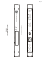
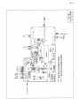
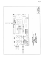
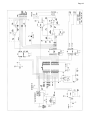
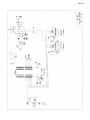
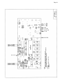
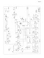
Page 3
to unrelated functions which should not be connected to the computer. (Software is also available
from the ESE Web-Site at http://www.ESE-WEB.com.)
12/24 Hr: The ESE “TC89” Time Code can be output in either 12 hour or 24 hour format. This enables
Remote Clocks to differ from the Master. Turn “ON” the “24 HR” DIP switch (switch #4 on the ES101 logic board) for 24 hour operation. Note: Most ESE Serial Time Code Reader Clocks can be
programmed for either 12 hour or 24 hour format regardless of the “TC89” format. To set the
display for 12 hour format, turn on DIP switch #4 on the ES-USS display logic board.
DST: DST (Daylight Savings Time) can automatically be compensated for if the end-user desires.
Turning “ON” the "DST" DIP switch (switch #6 on the ES-101 logic board) enables the DST feature.
The DST adjustment is according to the standards used in the United States and switches at 2:00
AM. Foreign DST standards are available on a "custom" basis.
Date: The date information encoded into the SMPTE time code is typically set to include Month-Day-Year
information. Turning “ON” the “DOY” DIP switch (switch #5 on the ES-101 logic board) reformats
the data to contain Day of Year (001-366) instead of Month-Day-Year.
OPTIONS
The rear-panel of the ES-102 provides access to all "Optional" inputs and outputs via various connectors (BNC &
DB-9). Please refer to the "Rear Panel DB-9 Connector Pin Designations" and "Specifications" for more details.
Time Codes
B: Option "B" provides a parallel BCD Output of the time data. The data is CMOS compatible and
contains 20 Data Lines (10’s Hours thru Seconds) and Ground. Applications requiring Parallel BCD
require an ES-169B (Serial To Parallel Time Code Converter) to be ordered separately.
Frequency Outputs
K: Option "K" provides a 1 KHz square wave, a 10 MHz sine wave and a phase coherent 1 PPS output.
The 1 PPS output has a 50% duty cycle and replaces the standard 50% duty cycle 1 PPS output. The
1 KHz and 10 MHz outputs are accessible on BNC connectors. The sine wave is 4 Vpp into 50 ohms.
Potentiometer R6 allows the output level of the sine wave to be adjusted by +/- 0.5 volts. The square
wave is 5 Vpp. A front panel 10 MHz Lock LED is provided. This LED lights solid to indicate that the
unit has “locked” to GPS and the outputs are within specifications. The 1 PPS output is phase
coherent when the 10 MHz Lock LED lights solid. The LED blinks if GPS “lock” has been obtained,
but the outputs are out of specifications. If “lock” has not been obtained, the LED does not light.
Option ‘45ηS’ is required.
The Option “K” system functions independently from the rest of the clock, although it receives its
input from the same GPS receiver as the clock system. When first powered up, the receiver searches
for satellites. When it locks on to at least one, the GPS Lock LED indicates a locked condition by
lighting solidly. The 10 MHz Lock LED begins flashing after a delay of about 40 seconds. The flashing
of this LED indicates that the GPS receiver is locked and that the 10 MHz system is in the process of
adjusting the frequency of the 10 MHz output. This process may take up to 1 hour. During this time
the frequency, if measured, may indicate 100 – 200 Hz off. This is normal during the locking process.
While the 10 MHz Lock LED is flashing, the output should not be used as a reference. When this LED
lights solidly, the output is within tolerance.
The ES-110M12 PCB generates the Option “K” outputs – 10 MHz & 1 KHz. The PCB receives 1 Hz
and satellite data from the GPS receiver on the main PCB. +12v & +5v power is also supplied to the
110M12 board. The system consists of a TCXO (temperature-compensated crystal oscillator), counter
chain, phase detector, loop filter and supervisory microcontroller (Z2). The 20 MHz oscillator is
divided by the counter chain (Z7-Z12 & part of Z5) down to 1 Hz. The phase-detector chip (Z4)
receives this signal and the 1 Hz signal from the GPS receiver. Z4 produces an output which is fed to
the loop filter, consisting of analog switch Z3, resistors R15 - R17, capacitors C22 - C23 and op-amp
Z17. The analog switch allows the microcontroller to control the time constant of the filter and also
disable the loop during periods of non-reception of satellites. The filtered control voltage is fed to the
frequency control input of the TCXO. This functions as a phase locked loop, controlling the frequency
and phase of the oscillator from the GPS reference 1 Hz. The satellite data from the GPS is fed to the
microcontroller UART input, allowing the system to know if the receiver is locked to satellites. The
microcontroller also monitors an output from the phase detector chip to determine the amount of
phase difference between the GPS and the internally divided 1Hz. If it is greater than approximately
40 milliseconds, the microcontroller “gear shifts” the counter chain fast or slow to bring the relative
phase to under 40 mS. This procedure is performed during initial lock-on, or if reception of satellites is
lost for a significant time and enough drift occurs. After rough phase adjustment is performed, the
oscillator frequency remains either fast or slow by about 100-200 Hz until the local 1 Hz arrives in