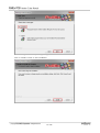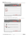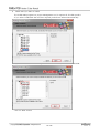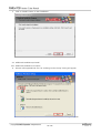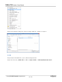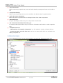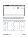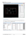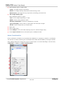
1
PollEx PCB Version 5 User Manual PollEx PCB V5.0 1 / 136 PollEx Introduction ....................................................................................................................................................... 7 PollEx Product Features ................................................................................................................................... 7 PollEx Licensing ..................................................................................................................................................... 8 PollEx Installation ................................................................................................................................................ 8 PollEx PCB Concept .......................................................................................................................................... 29 PollEx PCB Launching ............................................................................................................................ 30 PollEx PCB Windows ............................................................................................................................... 30 PollEx Menu Structure ........................................................................................................................... 31 Mouse Control ............................................................................................................................................. 36 File ......................................................................................................................................................................................... 36 File Open / Save ................................................................................................................................................. 37 File Close and Program Exit ........................................................................................................................ 38 Import ECAD ......................................................................................................................................................... 38 Altium / P-CAD Interface .................................................................................................................... 39 Altium Designer / Protel ............................................................................................................ 39 P-CAD ...................................................................................................................................................... 40 Cadence (Allegro/Spectra/OrCAD) Interface ....................................................................... 41 Cadence - Allegro/Allegro Expansion ................................................................................ 41 Cadence - Spectra/OrCAD ......................................................................................................... 47 Mentor Graphics Interface ................................................................................................................. 48 Power PCB ............................................................................................................................................ 48 Mentor Graphics - Board Station .......................................................................................... 49 Mentor Graphics - Neutral File ............................................................................................... 51 2 / 136 Mentor Graphics - Expedition ................................................................................................. 52 Zuken Interface ......................................................................................................................................... 54 Zuken - Cadstar(*.cpa) ............................................................................................................... 55 Zuken - CR5000 Board Designer ........................................................................................... 55 Zuken - CR5000 PWS .................................................................................................................... 57 Gerber Data Interface ........................................................................................................................... 60 PollEx ASCII Interface .......................................................................................................................... 60 Export Design to EDA vendor’s Formats ............................................................................................ 62 Ansoft ANF File(*.anf) ........................................................................................................................... 62 Ansoft SiWave File (*.siw) ................................................................................................................. 63 Sigrity SPD File ........................................................................................................................................... 63 AGILENT 3070............................................................................................................................................. 64 AGILENT ADS File ..................................................................................................................................... 65 Zuken HotStage (*.rif) .......................................................................................................................... 66 XTK(*.ISF; *.QNF) ................................................................................................................................... 67 Restricted PDBB ........................................................................................................................................ 67 Print ............................................................................................................................................................................ 70 Setting ................................................................................................................................................................................ 72 Environment .......................................................................................................................................................... 72 General ............................................................................................................................................................ 73 View ................................................................................................................................................................... 74 Layer - Initial View .................................................................................................................................. 76 Layer-Layer Stack..................................................................................................................................... 76 3 / 136 Tool - Picking ............................................................................................................................................... 77 Tool - PCB Explorer.................................................................................................................................. 78 Tool – Component Arrangement Plan ......................................................................................... 79 Tool – Composite-nets .......................................................................................................................... 80 Collaboration Engine .............................................................................................................................. 81 ECAD .................................................................................................................................................................. 82 ECAD - Cadence Allegro........................................................................................................................ 82 ECAD - Cadence Allegro Expansion .............................................................................................. 83 ECAD - Mentor Board Station, Neutral ....................................................................................... 84 ECAD - Mentor Expedition .................................................................................................................. 85 ECAD - PADS ................................................................................................................................................ 86 ECAD - Zuken CR5000 PWS ............................................................................................................... 87 ECAD - Zuken CR5000 Board designer....................................................................................... 88 ECAD - Gerber ............................................................................................................................................. 89 PollEx PCB’s Layer ............................................................................................................................................. 90 Layer ........................................................................................................................................................................... 90 Measure .................................................................................................................................................................... 91 Picking ....................................................................................................................................................................... 92 Unit Conversion ................................................................................................................................................... 93 Board Information ............................................................................................................................................ 94 View...................................................................................................................................................................................... 95 Set Capture Window ........................................................................................................................................ 95 Mirror View / Board Rotation .................................................................................................................... 96 4 / 136 Route on, off /Component on, off / Polygon Fill, Unfill ........................................................... 97 Net Display On/Off ........................................................................................................................................... 98 Board Mini-Map ................................................................................................................................................... 99 Menu-bar, Tool-bar, Status-bar ............................................................................................................... 99 Properties ....................................................................................................................................................................... 100 Nets ........................................................................................................................................................................... 100 Composite-nets ................................................................................................................................................. 101 Parts.......................................................................................................................................................................... 102 Material Library ................................................................................................................................................. 102 Layer Stack ........................................................................................................................................................... 103 Tools................................................................................................................................................................................... 103 PCB Explorer ....................................................................................................................................................... 104 Change Reference Names .......................................................................................................................... 106 Change Board Origin...................................................................................................................................... 107 Go to Location .................................................................................................................................................... 108 Component Arrangement Plan ............................................................................................................... 109 PCB Data Extractor ......................................................................................................................................... 110 Decap Extractor ................................................................................................................................................ 111 Net Color ................................................................................................................................................................ 112 Net Length View ............................................................................................................................................... 113 Net Analyzer ........................................................................................................................................................ 114 Gerber Transformation................................................................................................................................. 115 Visual Layer Composition ........................................................................................................................... 116 5 / 136 Composite-nets Generator ........................................................................................................................ 117 BOM Changer ...................................................................................................................................................... 119 Analysis ............................................................................................................................................................................ 121 Option ............................................................................................................................................................................... 122 Part Viewer .......................................................................................................................................................... 122 Net 2D/3D Viewer ........................................................................................................................................... 126 Padstack/Via Viewer ..................................................................................................................................... 129 Net Topology Viewer ..................................................................................................................................... 130 Attribute Finder ................................................................................................................................................. 131 PollEx CE ................................................................................................................................................................ 133 Manufacture ................................................................................................................................................................. 134 Red-mark ........................................................................................................................................................................ 134 Red-mark ............................................................................................................................................................... 134 6 / 136 PollEx PCB PollEx Introduction PollEx suite is knowledge based design-verification toolset for PCB. It provides functions for all processes from concept design – schematic design – layout – verification(validation) – manufacturing to make them is most effectively used. Also, it provides well customized environments which are widely used among various types of electronic process engineers. PollEx collects all functions which are used by design tool, manufacturing tool and process management solutions. With easy-to-use operation and versatile functions will guide users to the new electronic exploring. PollEx Product Features PollEx PCB – layout design viewer and basic module for other option modules. PollEx Logic – schematic design viewer. PollEx Cross Probe – difference checking module between PCB and PCB, schematic and schematic design and comparing module among PCB layout, schematic and BOM data. PollEx CAM – GERBER file viewing and editing module. PollEx BOM – ASCII or Excel formatted BOM(Bill Of Materials) reader. PollEx DFM – manufacturing rule based layout design checker (DFM : Design For Manufacturing). PollEx DFE – electrical rule based layout design checker (DFE: Design For Electrical Engineering. PollEx DFA – using 3D package library, assembly rule based layout design checker. PollEx SI – electrical analysis (signal integrity) tool using POLLIWOG SPICE engine. PollEx Thermal – board level thermal analysis module. PollEx VLSI – IC design data, GDSII file viewer. 7 / 136 PollEx Licensing Node Lock Floating Free Version Program download via web pages (http://www.polliwogeda.com) Lock Key FlexLM – Network License Stand – alone There are two types of PollEx license, node lock and floating license for purchasing version. Node Lock is stand-alone version which is usable at a specified node on network. Floating version is license type that all users on network can use license to the purchased number of limit. Free version is PollEx executable file not asking license. Users can get download free version on website, http://www.polliwogeda.com. Differences between purchasing and free version are followings, - PollEx PCB : free version doesn’t have save feature and cannot link with option feature. - PollEx Logic : free version is same. - PollEx CAM : purchasing version has editing feature. PollEx Installation 1. License Server Setup 1.1. FlexLM compatibility table O/S Compatibility FlexLM Version Windows XP √ Ver.9.2 to V11.9 Windows Vista √ Ver.9.2 to V11.9 √ Ver.11.9 Windows 7 or later Version 1.2. FlexLM 11.9 PollEx Server: FlexLM should be installed PollEx Client: Don’t need to install FlexLM 1.2.1. FlexLM 11.9 License Server setup A. Download FlexLM License Manager and install it. (Even though you already have FlexLM for other tools, you should re-install following FlexLM. PollEx deamon is pollex.exe. It is included in following download link) (We recommend that install FlexLM under Polliwog installed directory.) http://www.polliwogeda.com/download/FlexLM/FlexLM_v119.zip B. Execute lmtools.exe file from FlexLM installed directory. You should see the dialog box as shown below. C. Select the tab labeled: Config Services. 8 / 136 ① Assign the service a name: in this example we call it pollex. However if you have multiple FlexLM services you should identify which company's product is being licensed. ② Enter the full path or use the browse button to define the location of the license server program, lmgrd.exe. In this example we copied it into a directory called c:\Polliwog\FlexLM_v119. Note: Never use a directory with the name "artwork" anywhere in it: e.g. c:\flexlm\artwork. This is a known problem with flexlm (due to file locking behavior) and will not work. ③ Enter the name/location of the license file. In this example it is located in the directory called c:\Polliwog\FlexLM_v119 and it is called khkim-eval.lic. ④ Enter the name/location of the log file. This file can be useful if problems arise. - Click on “Browse” button. Explorer window will appear. - Navigate to FlexLM installation directory. - Enter the name of log file arbitrarily. (Do not use the same name with “Service Name”.) - Click on “Open” button to close the window. 9 / 136 Note: Log file name should be different with ‘Service Name’. ⑤ Check the box labeled: Use Services. This will install it as a Windows service. ⑥ Check the box labeled: Start Server at Power Up. Windows will start the flexlm service automatically each time the computer is rebooted. ⑦ Click on Save Service. D. Start Service - Select the tab labeled: Start/Stop/Reread. - Select license service “pollex”. - Click on “Start Server” button to start pollex license server. E. Review Service Status - Select the tab labeled: Server Status. - Click on “Perform Status Enquiry” button to get server status. - After a second or two details will appear in the text window. Scroll down and you can see which products are licensed, how many licenses are available and which users (if any) are accessing licenses. 10 / 136 1.3. Firewall setup Windows7 or later OS, in order to avoid firewall problem, you should register Pollex daemon files to Windows firewall. (lmgrd.exe and pollex.exe) 1.3.1. Firewall resister A. Register lmgrd.exe - On the Windows Start menu, point to “Control Panel”. - Click on “System and Security” icon. - “System and Security” window will appear. - Click on “Windows Firewall/Allow a program through Windows Firewall” icon. 11 / 136 - “Allowed Programs” window will appear. - Click on “Change settings” button to enable “Allow another program” button. - Click on “Allow another program” button. - “Add a Program” window will appear. - Click on “Browse” button. 12 / 136 - “Browse” window will appear. - Navigate to FlexLM installation directory. - Select “lmgrd.exe” file, click on “Open” button. - “Add a Program” window will appear. - Select “Flexera Software, Inc.”, click on “Add” button. 13 / 136 - “Allow Programs” window will re-appear. - You can find that “Flexera Software, Inc” file is registered. - Click on “OK” button to close window. B. Register PollEx.exe - On the Windows Start menu, point to “Control Panel”. - Click on “System and Security” icon. 14 / 136 - “System and Security” window will appear. - Click on “Windows Firewall/Allow a program through Windows Firewall” icon. - “Allowed Programs” window will appear. - Click on “Change settings” button to enable “Allow another program” button. - Click on “Allow another program” button. 15 / 136 - “Add a Program” window will appear. - Click on “Browse” button. - “Browse” window will appear. - Navigate to FlexLM installation directory. - Select “pollex.exe” file, click on “Open” button. 16 / 136 - “Add a Program” window will appear. - Select “Pollex daemon”, click on “Add” button. - “Allow Programs” window will re-appear. - You can find that “Pollex daemon” file is registered. 17 / 136 - Click on “OK” button to close window. 18 / 136 2. PollEx Installation You can obtain PollEx software from the Download Center of the Polliwog’s website. http://www.polliwogeda.com/download/InstallShield/PolliwogInstall_V5/PolliwogInstall_V5. exe The “Cygwin” program is required to run the PollEx SI software on Windows systems. You can install multiple copies of the different version of PollEx software on the same computer. 2.1. PollEx Software Installation There are two types of installation method, “complete” and “custom”. Follow these steps to install PollEx software: 2.1.1. “Complete” installation method A. Execute PolliwogInstall.exe file to launch “InstallShield Wizard”. - Click on “Next” for next step. The “License Agreement” dialog will appear. B. Check “I accept the terms of the license agreement” item, click on “Next” button. 19 / 136 - The “Polliwog Product Setup” dialog will appear. C. Enter ‘User Name’ and ‘Company Name’, click on “Next” button. - The “Setup Type” dialog will appear. D. User can select installation method, “Complete” and “Custom”. If you want to install all of PollEx software, check “Complete” item and click on “Next” button. 20 / 136 - The “Polliwog Product Setup” dialog will appear. Click on “Install” button to start installation. 21 / 136 2.1.2. “Custom” installation method A. Execute PolliwogInstall.exe file to launch “InstallShield Wizard”. - Click on “Next” for next step. The “License Agreement” dialog will appear. B. Check “I accept the terms of the license agreement” item, click on “Next” button. - The “Polliwog Product Setup” dialog will appear. 22 / 136 C. Enter ‘User Name’ and ‘Company Name’, click on “Next” button. - The “Setup Type” dialog will appear. D. User can select installation method, “Complete” and “Custom”. - If you want to install PollEx software products individually, check “Custom” item and click on “Next” button. - The “Select Feature” dialog will appear. 23 / 136 E. Check items you want to install. The “PollEx PM” program is a project management tool; it requires all of PollEx product. - If you select “PollEx PM” then all other required products are selected automatically. - If you want install “PollEx PCB” only, uncheck “PollEx PM” first, and select “PollEx PCB”. - Click on “Next” button. 24 / 136 F. Click on “Install” button to start installation. 2.2. Additional Installation/Uninstall 2.2.1. Additional Installation Procedure A. Execute PolliwogInstall.exe file. The “Polliwog Product Setup” dialog will appear. - Check “Modify” item, click on “Next’ button. The “Select Feature” dialog will appear. 25 / 136 B. In the feature list, select item you want to install. Or uncheck checked item you want to uninstall. ※ Example1: Install “PollEx Logic” and “PollEx CAM” additionally. ※ Example2: Uninstall “PollEx CAM”. 2.2.2. PollEx software Uninstall To uninstall PollEx software: - On the Windows Start menu, point to All Program > Polliwog>Uninstall. The installation wizard appears and guides you through the uninstallation process. 26 / 136 PollEx Launching 1. Check installed program list at “Start – Program – Polliwog”. Users can launch PollEx toolset depending on having license features. Below is procedure to install PollEx toolset. Below table shows PollEx toolsets and their executable files. Program Executable Options PollEx PCB PollExPCB.exe PollEx DFM/DFE/DFA/SI/Thermal Component Arrangement Plan/Component Arrangement Plan – Comp Placing Density/Attribute Finder/PollEx CE/Polygon Merge/Solder Quantity Calculator/ Metal Mask Manager/ Block JIG Generator/Gerber to PCB/Test-Point Location Generator/Router-Machine JIG Generator/Mounting Extractor/Underfill PollEx Logic PollEx PollExLogic.exe Cross PollEx Logic DFE PollExCP.exe Probe PollEx CAM PollExCAM.exe PollEx BOM PollExBOM.exe 27 / 136 Emulator/Mounting Data PollEx VLSI PollExVLSI.exe PollEx Magic Net PollExMN.exe UDVS UDVS.exe Unified Part PollEx SI/Thermal UPMS.exe Management System Unified Part Data UPViewer.exe Viewer Depending on users installation method, installed path might be different. And O/S can save lastly installed PollEx program path into registry information. There is no information to be removed in registry information during uninstall process. 2. Upon launching installed program, user can meet the dialog box to select usable PollEx version. Later this selection can be changeable thus purchased user can select right button menu, “PollEx Purchased/Evaluation Version” when user has released license. PollEx Using Environment To successfully install and run PollEx software your system must meet the following minimum requirements. 1. Recommended System Windows: 2003, XP, 7 (32-bit, 64-bit mode), 8 (32-bit, 64-bit mode) 28 / 136 PC with All multi-core processor Over 4GB RAM 2GB Hard Disk Space 32-bit Color Palette Mouse or compatible pointing device 2. Minimum System Windows: 2003, XP, Vista, 7 (32-bit, 64-bit mode), 8 (32-bit, 64-bit mode) PC with over 1GHz CPU Over 512MB RAM 1GB Hard Disk Space 32-bit Color Palette Mouse or compatible pointing device PollEx PCB Concept PollEx PCB can read ASCII files come from various types of ECADs or binary file having extension, PDBB. ASCII files from ECAD vendors are all different depending on ECAD suppliers. Users should know about the type of ECAD and their file extension before reading them in PollEx PCB program. Below table shows PollEx PCB supporting ECAD vendors and their ASCII files. ECAD vendors Altium Products File Extension Version PCAD *.pcb all Altium Designer *.pcb all Protel *.pcb all Allegro 1. *.brd, *.pad, *.rte, *.sym 2. *.comp, *.comppin, *.geom, *.lay, all *.net, *.pad Cadence APD After changing *.mcm to *.brd, use Allegro reading method. all Spectra *.dsn all OrCAD Layout *.dsn all Mentor BoardStation *.geom, *.nets, *.comp, *.traces all Graphics BoardStation *.neutral, *.geom, *.trace all 29 / 136 (Neutral) Expedition PowerPCB (PADS) (Valor) ODB++ CADSTAR ZUKEN CR5000 - Board Designer CR5000 - PWS Cell.hkp, JobPrefs.hkp, Layout.hkp, NetProps.hkp *.asc all 5.0~ Folder all *.cpa all Single board : pcf, ftf Arrayed board : pnf, ftf BSF, CCF, MDF, UDF, WDF EAGLE CAD BRD IPC2581 CVG CAM350 CAM 7.0 all RS-274D - all RS-274X - all Gerber CSiEDA WinPCB WinPCB extract PollEx PCB ASCII file, *.pdba 6.0 PollEx PCB (Binary) *.pdbb 3.0~ PollEx PCB (ASCII) *.pdba 4.0~ Polliwog If user has other format which is not supported by PollEx PCB, users can be supported UCS(User Customizing Service). PollEx PCB Launching Launch the menu, “Start -> Program -> Polliwog -> PollExPCB” Launch from the directory, “C:\Polliwog\V5\PollExPCB.exe” PollEx PCB Windows Below picture is the launched PollEx PCB main window. 30 / 136 ① Users can review the layout design at here, main window viewing area. ② At the top of main frame window, user can see the version of PollEx PCB and active file name and path. ③ Menu Bar gives users many useful functions. ④ Tool-Bar menu give users easy and institute icon menu. ⑤ Status-Bar menu shows current application status. ⑥ PollEx PCB shows the location of mouse cursor point. ⑦ Show the unit of active PCB layout design. ⑧ Picking-Tool box show the information of mouse-selected objects. PollEx Menu Structure PollEx PCB has 8 menus in menu bar. Menu File Sub-menu They will guide user to easily explore PCB layout. Short Description -cut Import ECAD Read various types of ECAD. Export to Export to EDA vendors’ data structure. Open PDB Binary File Ctrl+O Open saved PollEx PCB file. Save Ctrl+S Save into PollEx PCB file. Save As Save as different name PollEx PCB file. 31 / 136 Create project folder for data handling in case of Save As Project Print Ctrl+P Print into paper or Bitmap/Postscript image. Close Close active working. Recent PDBB File List Import recently worked file. Exit Exit from PollEx PCB. Environment Set default PollEx PCB using environments. Layer Setting SI/Thermal analysis. Alt+L Set/View PollEx PCB’s layer status. Measure Measure the distance between objects. Picking Check the properties of objects. Unit Conversion Change the unit of PCB layout. Board Information See the whole board information. Unified Part Libraries Link 3D Package Parts Libraries. Link Go back to previous viewing status(under Previous construction).. Next Zoom In Zoom Out Go to next viewing status(under construction).. +, wheel↓ -, wheel↑ Zoom in viewing status. Zoom out viewing status. Zoom Window Alt+W Zoom in for mouse two picking points. Zoom 1:1 Alt+1 PollEx PCB default design viewing status. Toggle 1:1 Ctrl+Ta b Go to default window and shows previous Zoom in area. Mouse View Set Capture Window Click & Save mouse clicked area into system buffer. Ctrl+C Mirror View Ctrl+M Shows mirrored PCB image. Board Rotation Rotate PCB for given rotation angle. Route On/Off Toggle for displaying routing pattern On/Off. Component On/Off Toggle for displaying component On/Off Polygon Fill Toggle for displaying polygon Fill/UnFill Display Setup Set status for displaying route/via/component. Net Display On/Off Toggle for displaying net On/Off. Board Mini-Map MenuBar Show current viewing area regarding to whole PCB layout area. Toggle for showing menu-bar On/Off. 32 / 136 Properties ToolBar Toggle for showing tool-bar On/Off. StatusBar Toggle for showing status-bar On/Off. Nets Show netlist and nets’ properties. Composite-nets Show all composite nets’ properties. Show partlist and linkage status with local part Parts library. Material Library Show materials’ properties. Layer Stack Show/Edit PCB layout Stack-Up. Find /Query Alt+Q Find or query for component and net. PCB Explorer Ctrl+F Explore components, nets or combinations. Change Reference Change reference names. Names Change Board Origin Go to Location Alt+G Component Arrangement Plan Tools Show the components’ placement status. Make document regarding components or nets. Decap Extractor Make list for decoupling capacitors on PCB. Net Color Change/Save colors of routing nets. Net Length View Make list for all nets’ length. Net Analyzer Make analyzing report for all nets on PCB. Analysis Thermal Resistance Calculator Show all signals’ return paths. Calculate thermal resistance. Gerber After reading Gerber file, change the origin of Transformation Gerber layers to fit with PCB design. Visual Layer Composition Option Move cursor point to the given location. PCB Data Extractor Signal Return Path Analysis Change the origin point of PCB design. Make user specific layers’ composition. Composite-nets Make composite net for which are connected Generator through passive device or passive chip device. BOM Changer Change ECAD Part Name based on BOM data. Signal Integrity Launch signal integrity analysis tool. Thermal Analysis Launch board level thermal analysis tool. Power Integrity Launch power integrity analysis tool. Part Viewer Parts viewer for all parts used in PCB design. Real PCB Assembly 3D assembled PCB viewer using 3D package link. Viewer Also provide the exporting to STEP. Net 2D/3D Viewer Show routing nets’ structure with 2D/3D. 33 / 136 Padstack/Via Viewer Padstack/Via viewer for all used in PCB design. Net Topology Viewer Show net structure as topology style. DFM Design For Manufacturing DFE Design For Electronics DFA Design For Assembly Attribute Finder Make property list for components and their pins. PollEx CE Design view sharing tool between remote displays. Make Board Paneling Make panelized board with active single board. Solder Calculate the quantity of solder used on PCB using Quantity Calculator solder or metal masks. Check metal mask with standard mask and generate Metal Mask Manager edited mask. Block JIG Generator Gerber to PCB Test-Point Generator for block-jig for mounting process. Alt+F12 Location into intelligent PCB design. Make TP(Test Point) file report. Generator Manufacture After reading ODB++ or GERBER file, make them Router-Machine JIG Using GERBER file, find bridging region and extract Generator input file for router machine. Using 3D package libraries, realized component Mounting Emulator Mounting mounting. Data Extract mounting machinery information. Extractor After load Underfill Area Data which is generated Underfill from DFA result, modify the data and save to file. Generate Soldering Pallet JIG data for wave Soldering Pallet soldering flow. Also validation checks for Soldering Pallet Specification. Red-mark Help Red-mark Feature to make comment on PCB design. About PollEx PCB Show the version of PollEx PCB and shortcut key list. PollEx License Mode Show/Change the PollEx license mode. PollEx Manual F1 Open PollEx PCB manual. PollEx PCB ToolBar PollEx PCB provides tool-bar for frequently used menus. ① File management functions. 34 / 136 - Close : close active design. - Open : open PDBB file. - Save : save active design into PDBB file. - Print : print current view status into paper or Bitmap/Postscript image. ② Measure/Picking tools. Provide the function to measure objects or find the properties of objects. Two dialog menus run as toggle mode. - Picking tool : for mouse selected objects, show all related properties on picking dialog box. - Measure tool : measure objects’ size or distance between various objects. ③ View control menu. - Zoom In - Zoom Out - Area Zoom : zoom area for mouse selected two points. - Zoom 1:1 : go back to default view status. ④ PCB Explorer. - Using PCB Explorer, user can search components or nets and component/net composition. ⑤ Layer Control. - Artwork Layer : view layers with artwork layer order. - Physical Layer : view layers with physical layer order. - Layer Setting Tool : for selecting layers, user can change layer viewing status or layer properties. ⑥ Object Display On/Off Control. - Route On/Off : display On/Off function for route pattern. - Component On/Off : display On/Off function for components on PCB. - Polygon Fill/Unfill : display polygon or copper fill/unfill function. ⑦ Object Viewers/ Data Extraction Tool. - Parts Viewer : list and see all parts used in PCB layout. - Pad Stack / Via Viewer : list and see all padstacks and vias used in PCB layout. - Net 2D/3D Viewer : list and see all routing nets on PCB layout. - PCB Data Extractor : documentation tool for nets or components and their related properties and objects. After making table, user can extract table information into MS/Excel sheets. - Net Topology Viewer : show net routing structure with topology style. ⑧ DFM Core Running - Using this function, user can run PollEx DFM checking after specifying multiple DFM input files. 35 / 136 ⑨ DFE Core Running - Using this function, user can run PollEx DFE checking after specifying multiple DFM input files. ⑩ Metal Mask Manager - Metal mask data can be changed depending on manufacturing process. But in ECAD systems, it is allowed only one mask data. “Metal Mask Manger” can change mask data and compare them to standard metal mask database to check whether they are valid or not. ⑪ Gerber to PCB - After reading ODB++ or GERBER file, make them into intelligent PCB design. ⑫ Board Information Window - Window menu provide all information of working PCB. At dialog window, user can see file path, file generation date, board size, number of used component and nets… etc. ⑬ Window Image Capture Function - Using this menu, for selecting region with two points mouse picking and shortcut key, “Ctrl+C”, user can easily get image file on PCB. Mouse Control To efficiently operation, PollEx PCB provides some useful mouse operations. 1) Window zoom control: Zoom In/Out, mouse wheel up/down. 2) Panning: Window scroll, mouse right button click + Move. 3) Picking: use mouse left button. And if picking tool is active status, all selected objects’ information will be shown on picking tool. File Here, user can check basic functions, importing ECAD files into PollEx PCB and exporting working design to 3rd party EDA vendors’ format. 36 / 136 ① File Open and Save - Open PDB Binary File : import PollEx PCB’s binary file, *.PDBB. - Recent PDBB File List : import design from recently opened list. - Save / Save As : save active design into *.PDBB or different name of PDBB file. - Save As Project : create folder for data handling. ② File Close and Program Exit - Close : close working job file. - Exit : close PollEx PCB program itself. ③ Import ECAD Import design from ASCII file which are created by other EDA vendors’ CAD tools. PollEx PCB supports various types of prominent ECAD vendors’ format. ④ Export To PollEx PCB can export current design into various types of EDA vendors’ format. Many of them are analysis application’s neutral file format. ⑤ Print PollEx PCB can print active window image into printer or images like bitmap or postscript style. File Open / Save PollEx PCB’s binary data file has PDBB extension. After reading ASCII file from ECADs, using PollEx PCB, user can save or import these file into PollEx PCB. - Using the menu, “PollEx PCB >> File >> Open PDB Binary File” (Short cut key : “Ctrl + O”) - Using the menu, “Recent PDBB File List” Upon selecting design from recently used PDBB file list, user can easily open file. If user did not save design file or unstably closed case, that design is not stored into the recently file list. 37 / 136 - Save / Save As. Use this menu to save current design to PDBB file. The one of merits of PDBB file is small file size compare to original ECAD design file. So sending design to others or management will also be easy and fast without any loss of information. - Save current design using the menu, “PollEx PCB >> File >> Save/Save As”. (Short cut key is “Ctrl + S") File Close and Program Exit User can use this menu to close active design or exit from PollEx PCB program. - Close active design using the menu, “PollEx PCB >> File >> Close” - Exit from PollEx PCB using the menu, “PollEx PCB – File - Exit” Import ECAD All ECAD tools have their ASCII structure to be used by 3rd party applications. PollEx PCB can import those ASCII files from various ECAD vendors. Depending on different types of ECAD ASCII files, this manual provides the way of importing them. - Use the menu, “PollEx PCB >> File >> Import ECAD >> Select ECAD Tool” to read ECAD’s ASCII file. 38 / 136 ⑥ ECAD vendors list which PollEx PCB can import. ⑦ CAM350, Gerber file importing menu. ⑧ Files, generated by PollEx PCB. The purpose of GERBER file reading is to compare GERBER to PCB layout design. So the number of readable GERBER layers has limitation in PollEx PCB. As the purpose of reviewing GERBER file, PollEx CAM is recommended. - Also, complete same job using the menu, “Click mouse right button on working window >> Showing Pop-Up window as below picture >> Select ECAD Tool”. Altium / P-CAD Interface PollEx PCB supports various Altium’s CAD design files, Protel and PCAD. Altium Designer / Protel Step1. Extract Altium Protel ASCII file, *.PcbDoc in Altium Designer/Protel. Step2. Use the menu, “PollEx PCB >> File >> Import ECAD >> Altium – Protel”. 39 / 136 Step3. At file selection dialog box, select the target ASCII file, *.PcbDoc to import it. P-CAD Step1. Extract PCAD ASCII file, *.pcb in Altium Designer/Protel. Step2. Use the menu, “PollEx PCB >> File >> Import ECAD >> Altium(PCAD/Protel)-Accel”. 40 / 136 Step3. At file selection dialog box, select the target ASCII file, *.pcb to import it. Cadence (Allegro/Spectra/OrCAD) Interface Cadence do not support ASCII extraction menu itself, but users can use executable file, “extracta.exe” to get ASCII files. To use this command, users do not need license but Allegro installation environment. In PollEx PCB has two ways of reading Cadence Allegro design, Allegro and Allegro Expansion. It is because “Allegro” cannot describe abnormal pad but “Allegro Expansion” can handle it. So depending on way of importing types, resulted PDBB file could be different in file size. Cadence - Allegro/Allegro Expansion 1) Direct Allegro file reading using binary file, *.brd. 2) Allegro file reading using ASCII files. 41 / 136 1) Direct Allegro file reading using binary file, *.brd. Step1. Setup Environment for Interface Once user set environment for Allegro, every time when users import Allegro file in PollEx PCB, user don’t need any other additional setting. ① Select item, “PollEx PCB >> Setting >> Environment >> ECAD >> Cadence – Allegro”. ② Set the default reading type whether user import design from binary or ASCII file. ③ If user wants to use the way of reading binary file, set executable command file, “extracta.exe” path. Example) "Allegro Installation folder\tools\pcb\bin" ④ To use Allegro ASCII extraction command, “extracta.exe”, user need to use control file for extract ASCII file. Set the path for control file. Example) : "PollEx tool Install path\share\ExtractAllegro.out" 42 / 136 ⑤ Select item, “PollEx PCB >> Setting >> Environment >> ECAD >> Cadence – Allegro Expansion”. ⑥ Set the default reading type whether user import design from binary or ASCII file. ⑦ If user wants to use the way of reading binary file, set executable command file, “extracta.exe” path. Example) "Allegro Installation folder\tools\pcb\bin" ⑧ To use Allegro ASCII extraction command, “extracta.exe”, user need to use control file for extract ASCII file. Set the path for control file. Example) : "PollEx tool Install path\share\ExtractAllegro.out" ⑨ Check whether user want to use break component or not. “Break Component” means reference components which are different than prototype in library. ⑩ Check when user wants to read the design from Allegro version 16.3. Step2. Allegro design reading using original binary file, *.brd. – use one of following two ways. “PollEx PCB >> File >> Import ECAD >> Cadence – Allegro” “PollEx PCB >> File >> Import ECAD >> Cadence - Allegro Expansion” 43 / 136 Item ① and ③ are showing the contents set on environment. At ② and ④, select the Allegro binary file, *.brd and press the button menu, “ Read from Binary" will start reading Allegro file. If the check box ⑤ is ON status, PollEx PCB Allegro reader will check Allegro version whether it is version 16.3 or not. ① “Add Hole” : For the design file created by Allegro version 16.3, if there is another defined hole on certain layer, give the hole layer name. Using the environment setup, user do not need to setup Allegro reading parameters at this window. - “Cadence – Allegro” 44 / 136 After reading completion, PollEx PCB executes “extracta.exe” with background mode. And, at Allegro design file, *.brd locating folder, 4 ASCII files will be generated. They are *.brd, *.pad, *.rte and *.sym. Actually, PollEx PCB read these 4 files after running “extracta.exe” command. - “Cadence – Allegro Expansion” 45 / 136 As the same with Allegro reading case, Allegro Expansion reading also left some of ASCII files. In this case there are 6 ASCII files, *.Comp, *.CompPin, *.Geom, *Lay, *.Net and *.Pad. Actually, PollEx PCB read these 6 file after running “extracta.exe” command. 2) Allegro file reading using ASCII files. Step1. Extracting ASCII File Following two window guide user to extract ASCII file from Allegro binary design file, *.brd. - Allegro Reading Case. Use the Allegro ASCII file extraction command, “AllegroASCIIExtractor.exe” in the path, “PollEx Install Path \share”. At column ③, specify the Allegro ASCII extraction command file, “extracta.exe” location path. At the column ④, give the control file, “ExtractAllegro.out” path under “PollEx Install path\Share”. And column ⑥, select target Allegro design file and ASCII file saving path. Upon pressing the button, “Extract ASCII Design File” will make 4 different ASCII files. - Allegro Expansion Reading Case. Use the Allegro ASCII file extraction command, “AllegroExpansionASCIIExtractor.exe” in the path, “PollEx Install Path \share”. At column ③, specify the Allegro ASCII extraction command file, “extracta.exe” path. At the column ⑤, give the control file, “AllegroExpansion_ExtractCommandFile.txt” path under “PollEx Install path\Share”. And column ⑥, select target Allegro design file. 46 / 136 Upon pressing the button, “Extract ASCII Design File” will make 6 different ASCII files. Step2. Import Allegro using ASCII file. Use one of following two menus to import Allegro design. “PollEx PCB >> File >> Import ECAD >> Cadence – Allegro” or “PollEx PCB >> File >> Import ECAD >> Cadence – Allegro Expansion” ① To read Allegro design with ASCII file, the reading type check button should be “Read from ASCII File.” User can set this setting in environment. Using the button ②, for Allegro reading and button ③ for Allegro Expansion reading, users can select ASCII files. Finally, upon pressing the button, “Read from ASCII”, import selected ASCII files and convert them to PollEx PCB design job file, *.PDBB. Cadence - Spectra/OrCAD The file extension of Cadence Spectra is *.dsn. And, schematic file of Cadence OrCAD has also same file extension, so be cautious when user select file. 47 / 136 Step1. Extract ASCII file, *.dsn from Cadence Spectra. Step2. Use the menu, “PollEx PCB >> File >> Import ECAD >> Cadence Spectra/Cadence”. Another way of reading Spectra file is using utility program of Allegro. Using Allegro utility program convert Spectra file to Allegro design file, *.brd and use Allegro reader in PollEx PCB. Mentor Graphics Interface Mentor Graphics is releasing several different ECAD tools, Board Station, PADS PowerPCB and Expedition. Power PCB Users can export Mentor Graphics/ PowerPCB’ design to ASCII file, *.asc. Depending on ASCII version of PowerPCB, they might be different, but PollEx PCB will support every version of them. Use the menu, “PollEx PCB >> File >> Import ECAD >> PowerPCB – PADS” 48 / 136 ① After selecting menu, “Power PCB ASCII(*.asc)”, press the button menu, “Read from PADS ASCII” to read file. ② Setting this column is optional. Among ECAD artwork layers, specify component outline layers for top and bottom. PollEx DFM will use these layers’ data for measure base. ③ If there is the specific layer for board contour, give that layer name. This layer will be transfer to layer number 21 in PDB structure. ④ If there is the specific layer for drill, give that layer name. This layer will be transfer to layer number 22 in PDB structure. ⑤ "Signal Layer in Part Section”: In footprint definition, if object layer is signal layer, check this option. “Signal Layer in Line Data Section”: In board figure definition, if object layer is signal, check option. “Level 0 is Board Outline”: Check this option, if layer level 0 is board contour layer. “CAM Pad Over Size (Solder, Paste)”: Check this option if solder mask definition is recorded in CAM. “Line Width of COC as 0” : Check this option if line width of COC as 0. “Generate Teardrops” : This option is used automatically generate teardrop shape at PAD and Via. ⑥ Use this button to save above setting as default. Mentor Graphics - Board Station PollEx PCB’s Mentor Graphics - Board Station reader use following 5 ASCII files. File Example 49 / 136 comp.com_XXX comps.comp_256 net.net_XXX nets.net_123 traces.traces_XXX traces.traces_123 tech.tech_XXX Tech.tech_123 geometry file *.geom In Board Station working folder, there are 4 files except Geometry file. And among many files, select file having header, comp, net, and trace and tech files having highest revision number. It means they are latest files. But, user does not need tech.tech_XXX file, if user did not use blind or buried via. Step1. Extraction Geometry files in Board Station. 1. Open Job file and launch librarian. 2. Use the menu, "File-Save-Save ASCII Geometries" 3. Select "All Geometries" and "One File" and save file in certain path with extension, *.geom. Step2. Reading Mentor Graphics Board Station ASCII in PollEx PCB. Use the menu, “PollEx PCB >> File >> Import ECAD >> Mentor Graphics - Board Station”. ① Select reading board type. “Single Board”: use this checking option for reading single board. “Array-Single Board”: use this checking option for reading array board contour and single board. “Array-Full Board”: use this checking option for reading array board contour and full single board. ② Check this option when user use generic parts in array board and want them to be part of sub board. ③ Add Drawing Part to Reference Designator ④ Specify the folder in which ASCII data exist. 50 / 136 ⑤ At any column if user select one among 5 ASCII files, others are automatically assign into each folder column. At this time, if there are multiple files having same name but different version, PollEx PCB will automatically select the latest version. ⑥ Pressing OK button start reading interface. Mentor Graphics - Neutral File PollEx PCB also can read Board Station’s neutral file and followings are necessary ASCII files for importing into PollEx PCB. File Example neutral_file neutral.vss traces.traces_XXX traces.traces_123 tech.tech_XXX tech.tech_123 geometry file *.geom If user did not use blind/buried via, tech.tech_XXX file is needless. Step1. Extract Geom file in Board Station 1. Open jog file and launch librarian. 2. Use the menu, "File-Save-Save ASCII Geometries". 3. Select "All Geometries" and "One File". And save file with extension name *.geom into a certain folder. Step2. ASCII importing in PollEx PCB. Use the menu, “PollEx PCB >> File >> Import ECAD >> Mentor Graphics - Neutral File”. 51 / 136 ① Choose the type of ASCII file. “Neutral Only” will read only component placement information and netlist information. There is no routing information. But, “Whole Files” will read all PCB related information. Using “Whole Files” selection, PollEx PCB will read 4 files, tech.tech***, neutral, ASCII_GEOM and trace.trace***. ② Select working file’s path, then PollEx PCB will find necessary files at specified path. ③ User can select necessary files individually. Pressing OK button will start reading design data. Mentor Graphics - Expedition PollEx PCB read Mentor Graphics/Expedition’s 6 ASCII files. Following table shows all necessary files and their information. File Name Description Cell.hkp Component placement information JobPrefs.hkp Layer information 52 / 136 Layout.hkp Routing information NetProps.hkp Net information Padstack.hkp Padstack information PDB.hkp Part library information Use the menu, “PollEx PCB >> File >> Import ECAD >> Mentor Graphics – Expedition”. After selecting all 6 files, pressing OK button will start reading Expedition into PollEx PCB. 53 / 136 ODB++ ODB++ is ASCII format of Mentor Graphics to complement the weakness of GERBER format. Thus, it has all intelligent design information. PollEx PCB also supports this format. To import ODB++ file, use the following menu, “PollEx PCB >> File >> Import ECAD >> ODB++”. ① Specify the unit of PDBB not of ODB++. ② If the ODB++ file is come from Genesis, data file may have attribute of objects in “sysattr.dat”. Specify the attribute file before reading. ③ Select ODB++ compressed file. Also, define additional option about uncompressing path. The folder is created in the uncompressing path. ④ If the ODB++ file system exists as folder structure, select the top level folder in hierarchical folder structure. ⑤ Select top folder in folder searching dialog window. Zuken Interface PollEx PCB supports various Zuken’s CAD design files, Cadstar, Board Designer and PWS. 54 / 136 Zuken - Cadstar(*.cpa) PollEx PCB read Zuken CADSTAR file with ASCII having extension, *.cpa. Use the following menu, “PollEx PCB >> File >> Import ECAD >> Zuken - Cadstar(*.cpa)” Select *.cpa and pressing OK button start reading Zuken CADSTAR design. Zuken - CR5000 Board Designer PollEx PCB can read Zuken BD (Board Designer) ASCII file. Upon using the utility, user can extract ASCII file from Zuken BD’s binary design, *.pcb. Step1. ASCII files extraction using utility command, “BDExtractor.exe”. PollEx PCB supports two types of board types, single and arrayed board to read Zuken Board Designer. Array board file, *.pnf should have single boards information in it and at same time, single board files, *.pcf should also exist at certain folder. 55 / 136 To get ASCII file from Zuken BD, use the utility command, “BDExtractor.exe". Using this command, user can extract single and array board. File location is under “C:\Polliwog\V5\Share\BDExtractor.exe”. After specifying design file, *.pcb, press the OK button to start ASCII file extraction. Step2. Importing design into PollEx PCB using ASCII files. Use the menu, “PollEx PCB >> File >> Import ECAD >> Zuken - CR5000 Board Designer”. 56 / 136 ① Select the board type between single board and arrayed board. ② For the single and array board, user can define the layer name of board contour layer. And user can also define the rule to read as many as number of single boards or just one for same type board during arrayed board reading case. ③ Specify the layer name in Board Designer to be used with hole data layer in PDB. ④ PollEx PCB read 2 ASCII files, *.pcf and *.ftf, but it is enough to specify *.pcf. PollEx PCB automatically find *.ftf file in same folder. For reading array board, another two files, *.pnf and *.ftf are necessary. Zuken - CR5000 PWS PollEx PCB supports two types of reading, artwork and wiring modes for Zuken PWS. Artwork mode means that all objects in design have no intelligent information like net name. All routing patterns exist on physical layers but because they don’t have net information, so they will be transfer to just graphic data. In this case, after reading design with artwork mode, user cannot use these design for nets related function or for electrical analysis. All needed ASCII files are following 5. *.BSF Board specification information file. *.CCF Net information file. *.MDF Part information file. *.UDF Component placement and board graphic information file. *.WDF Routing pattern information file. 57 / 136 Use the menu, “PollEx PCB >> File >> Import ECAD >> Zuken - CR5000 PWS”. Among the 5 files, select any one of them and PollEx PCB can detect all other files and automatically read design. 58 / 136 To define usage of artwork layers in PWS, it is prefer to define all top/bottom corresponding layers. 59 / 136 Depending on users, they are using different layer mapping table in BSF. These layer mapping status can be saved into file, *.zls and re-use it for next reading. Gerber Data Interface PollEx PCB supports four types of GERBER formats, 274X, 274D, Drill and Square Hole. When you import Gerber Data, PollEx PCB analyze the file format internally and separate to 274X, 274D, Drill file, Square Hole and Aperture. In case of 274D, there are necessary both of Gerber data and Aperture file. If there are multiple aperture files, PollEx PCB make to one aperture data based on D-Code. Use the following menu, “PollEx PCB >> File >> Import ECAD >> Gerber(RS-274D/RS-274X)”. PollEx ASCII Interface PDBB file is PollEx PCB’s binary design file including all geometries and entities necessary to describe whole PCB design. Also PollEx PCB provides same ASCII file structure, *.pdba. This is ASCII version of PDBA file. Step1. Exporting design to ASCII file, *.PDBA in PollEx PCB. Use the menu, “PollEx PCB >> File >> Export To >> PDB ASCII V5(*.pdba)”. 60 / 136 After using above menu, at file saving dialog box, specify the file name and path to export into ASCII file. Step2. Reading ASCII file, *.PDBA in PollEx PCB. Select the file in dialog window and pressing OK button will start reading ASCII file, *.PDBA into PollEx PCB. 61 / 136 Export Design to EDA vendor’s Formats PollEx PCB supports exporting to other EDA vendors’ format. Use the menus under command, “PollEx PCB >> File >> Export To” PollEx PCB can export 7 different types of EDA vendors. They are ANSYS ANF File, Ansoft SiWave File, Sigrity SPD File, AGLENT 3070, AGILENT ADS File, Zuken Hostage, and XTK. Ansoft ANF File(*.anf) Use the menu, “File >> Export To >> ANF File” 62 / 136 Ansoft SiWave File (*.siw) Using this menu, user can export file to be used in Ansoft SiWave. To do this work, use the menu, “PollEx PCB >> File >> Export To >> Ansoft SiWave File”. Input default value for passive device. And to distinguish passive devices, let PollEx PCB know what the prefix of reference name of passive device. “OK” button will export file. Sigrity SPD File Use the menu, “PollEx PCB >> File >> Export To >> Sigrity SPD File” 63 / 136 All parameters are used in Sigrity tool and PollEx PCB provides all default values for them. If user wants to change some parameters, control them and pressing OK button will export file. AGILENT 3070 Use the menu, “PollEx PCB >> File >> Export To >> AGILENT 3070”. PollEx PCB supports AGILENT i3070 format and also exports location report for test point. 64 / 136 AGILENT ADS File Use the menu, “PollEx PCB >> File >> Export To >> AGILENT ADS File”. 65 / 136 Zuken HotStage (*.rif) Use the menu, “PollEx PCB >> File >> Export To >> Zuken HotStage File”. 66 / 136 XTK(*.ISF; *.QNF) Use the menu, “PollEx PCB >> File >> Export To >> XTK”. Restricted PDBB Using this feature, user can save some parts of whole board, after selecting nets and connected components for selected nets. In case of sending design to outer but if users do not want to whole board with security issues, this feature is effective. Use the menu, “PollEx PCB >> File >> Export To >> Restricted PDBB”. Upon launching “Restricted PDBB” menu, user meets following dialog menu to save partial design. 67 / 136 User has three options for saving design. One is saving component placement information only (①). Another is saving selected area only (②) and the other is saving design depending objects and related objects (③). ① Select “Export Component Only” button menu to save design for only components placement. At this status, routing and non-electrical information will be excluded at saving. ② “Export Selected Area Only” will give users two selection method. One is selecting rectangle area and the other is selecting arbitrary area. ③ “Export by Object Selection Method” will give users two selection menu windows. Combining two windows’ selections, user can select objects. If “Window 1” selection is “Component”, “Window 2” selection will be “Net”. If “Window 1” selection is “Net”, “Window 2” selection will be “Component”. It means user can select component and its connected net and net and its connected component. Using “Search” button menu, user can find necessary objects in “Window 1”. - “Automatically include other connected component” If “Window 1” selection is “Component”, “Window 2” selection will be “Net” automatically. In this case, and if this checking is turn on status, PollEx PCB will save also save include other side component also. 68 / 136 - “Show Composite Net Passive Component” If user selected components and they are connected with passive device, PollEx PCB will include passive device for saving when this option is turn on status. - “Select All” Select all items in “Window 2”. - “Display” Show selections on “PCB Viewing Area”. - “Exclude” Show selections on “PCB Viewing Area” with hidden for unselected objects. - “Clear” Reset window display. ④ - “Exporting Option” “Initialize stack-up information” PollEx PCB will reset stack-up information and make it with default value. - “Initialize Artwork Layer information” PollEx PCB will reset artwork layer information and make it with default value. - “Remove Board-Contour” PollEx PCB will remove board contour data and make it with basic rectangle geometries. - “Initialize Component Name” PollEx PCB will remove all part’s name information and rename them with string starting “PartXXX”. All other footprint, package and device name will be re-arranged. Vias and padstacks name will be re-arranged also. - “Initialize Net Name” PollEx PCB will remove all nets’ name and rename them with string starting “NetXXX”. Vias and padstacks name will be re-arranged also. 69 / 136 - “Initialize Net/Component Property” PollEx PCB will remove all properties assigned to net and components (reference designator). - “Include Component Outline” PollEx PCB will include all component outline of component(Artwork Layer-201: COC Top, 202: COC Bottom). - “Include Solder Mask” PollEx PCB will include all solder mask layer. - “Include Metal Mask” PollEx PCB will include all metal mask layers. - “Include Board Figure” PollEx PCB will include all board figures. - “Include Mechanical Objects” PollEx PCB will include all mechanical objects(Component Figure Data). ⑤ Using “Save As” menu, save current status into different PDBB file. Print PollEx PCB’s “print” feature supports two types of formats. 1) Bitmap Use the menu, “PollEx PCB >> File >> Print”. “Print Paper Size Ratio”: real size regarding to the PCB. “Quality”: the scale of resolution. 2) Postscript. To print out postscript file, use the menu, “PollEx PCB >> File >> Print”. “Real Size”: print out size as same as real PCB size. 70 / 136 “Complementary Color”: define the color of printing. “Current View Area”: print out same as viewing status. 71 / 136 Setting Under setting menu, there are many setting items for defining default value for using PollEx PCB. Use the menus under “Setting” in main menu. ① Environment ② Layer ③ Measure ④ Picking ⑤ Unit Conversion ⑥ Board Information Environment Using this menu, users can set-up defaults for using PollEx PCB. Setting items are, - whether user set password during saving operation for design open - working file path - display method - default language for menu and manual - default setting for different ECAD reader Use the menu, “PollEx PCB >> Setting >> Environment”. 72 / 136 ⑦ Classification for environment setting items. ⑧ Each item’s parameter setting window. ⑨ User can load or save environment setting. So multiple users can share setting to use same environment. General ① At this, user can set language and default file path. 73 / 136 ② “File Search Default Path”: set default file open path for PollEx PCB. ③ “Log File Save Directory”: set default log file saving path. ④ “PDBB Compress”: define whether user can compress file or not during saving PDBB file. ⑤ “PDBB Encryption”: define whether user input password or not during saving PDBB file. If user checks this option, user may meet following password input window before saving file. ⑥ “Excel Export”: set default MS/Excel exporting path. ⑦ “Language”: set default language for using. PollEx PCB supports English/Chinese/Japanese/Korean. To use Chinese or Japanese, user should install proper window language. ⑧ “Automatic Update”: set default directory for InstallShield file. file in folder, user can update PollEx PCB automatically. View ① Setting window for display. 74 / 136 If user has PollEx InstallShield ② “Draw Mouse Cross Line”: for mouse cursor point, show it with “+” mark. “Foreground Selected Route”: during picking operation, if there are multiple patterns are overlapped, selected pattern will be shown at top. “Auto Zoom”: Upon using “PCB Explorer”, “Highlight” or “Exclude” operation shows objects with auto zoom-in. “Fill Selected Route”: for selected routing pattern, show them with filled shape. “Zoom to Mouse Point Area”: zoom area based on mouse point. ③ Grid Set the distance of grid and decide whether PollEx PCB shows grid or not. ④ Set Capture Window Use the menu to make partial image capture, screen capture, full area capture. ⑤ Zoom Decide ratio for zoom. ⑥ Measure “Dimension Text Scale”: set the dimension’s size using measure function. “Decimal Point”: set the decimal point for measure resulting. Select the value 1~5. “Display”: decide handling for under decimal point. Select one among ceiling, round and floor. ⑦ “Net Color Display”: if source ECAD file has its original color setting for routing nets, this setting will decide whether PollEx PCB show original ECAD color or use default PollEx PCB color. “User Windows Operation”: for zoom In/Out and panning operation, operations will be applied reversely. 75 / 136 Layer - Initial View ① Set the default PDBB file’s open status for color, display and layer display on/off status. ② "Default Layer View” Set layer’s displaying status for top/bottom/inner layers. For the huge size file, checking top only is very effective for opening speed. ③ "Display” For objects on PCB, set the objects showing status. “Route On”: initially PollEx PCB display routing pattern. “Component On”: initially PollEx PCB display components. “Copper Fill”: initially PollEx PCB shows copper pour as filled shape. ④ “Physical Layer Definition” Decide for showing top/bottom component related layer displaying status. ⑤ “Artwork Layer Color Setting” PollEx PCB can define the artwork layers’ default color. Layer-Layer Stack ① Set the PCB physical layer’s composing materials. 76 / 136 ② Define the PCB’s conducting and di-electric material from material library. ③ Define the conducting layer’s default thickness values. Tool - Picking ① Set the default parameter for using picking tool. 77 / 136 ② “Component” when user picked component, this option tell PollEx PCB what attributes are displayed or not. ③ “Route” when user picked route data, this option tell PollEx PCB what attributes are displayed or not. ④ “Display Component Information” ⑤ “Pin Number”: decide whether show pin number or not in picking tool operation. “Select Priority” Select priority among component/pin/route. Tool - PCB Explorer ① Set the default value for using PCB Explorer. ② If this option is checked, PCB Explorer will be launched after opening PollEx PCB job file. 78 / 136 ③ Set the upper window’s object status after launching PollEx Explorer. ④ Set the lower window’s object status after launching PollEx Explorer. ⑤ In PDB data structure, there are two name properties, part name and ECAD part name. If there is broken component case, unique identifier, part name will be given differently than that is assigned in ECAD tools. Decide what name will be used in part selection window. Tool – Component Arrangement Plan ① Set the default values for using “Component Arrangement Plan” tool. ② Set “Component Arrangement Plan” tool’s environment file, *.cpas and input file path. 79 / 136 Tool – Composite-nets ① "Composite-nets”: composite-nets are combined nets through passive device. PollEx PCB can merge two or multiple single net into composite net. 80 / 136 ② “Net Classification” While constructing composite net, user can decide whether power/ground nets are included or not. ③ “Component Setting” While constructing composite net, user can define the default values for passive device. ④ “Prefix of Passive Component” Define the prefix for passive device to distinguish them from other components. ⑤ “Part Name Type” Set part name type to define the pivot components from librarian. ⑥ “Pin Connection Information File Path(*.pci)” For arrayed passive part define the pin connection information and load it to make composite nets. ⑦ “Composite-nets List” - “MAX Number of Composite Components”: set the maximum number of passive devices. - “Except Net Name as Prefix from List”: set the net name prefix which are excluded from making composite net. Collaboration Engine ① Using collaboration tool, users in remote locations can share the display with PollEx PCB. 81 / 136 ② “Default Fort Number” Define the default remote machine’s port number to connect. ECAD ① Default environment setting to import ECAD. ② This section allows you to set the encoding method of ECAD. if you want to convert EUC(Extended Unix Code)-JP to Shift JIS, check this option. ECAD - Cadence Allegro Cadence Allegro doesn’t support ASCII out feature, but support command utility, “extracta.exe”. “extracta.exe” is impossible to run alone. It require Allegro installation environment. But it does not ask any license. “Allegro” cannot describe abnormal pad but “Allegro Expansion” can handle it. So depending on way of importing types, ① Default environment setting to import Cadence Allegro design. 82 / 136 ② ”Default read Type” - “Read from Binary File”: support default as Allegro binary file reading. - “Read from ASCII File”: support default as Allegro ASCII file reading. ③ “Path to the extracta.exe” Allegro’s ASCII extraction command utility file, “extracta.exe” location. In general case, this file is located in “Allegro Install path\tools\pcb\bin”. ④ “Path to the Control File” Allegro’s ASCII extraction control file, “ExtractAllegro.out” location. In general case, this file is located in “PollEx Install path\Share\ExtractAllegro.out”. ⑤ “Layer Set-Up” Set Allegro layers’ name which will be used as PDB’s component related layers for silkscreen, component outline layer. ECAD - Cadence Allegro Expansion Cadence Allegro doesn’t support ASCII out feature, but support command utility, “extracta.exe”. “extracta.exe” is impossible to run alone. It require Allegro installation environment. But it does not ask any license. ① Default environment setting to import Cadence Allegro design for support abnormal pads. 83 / 136 ② “Default read Type” - “Read from Binary File”: support default as Allgero binary file reading. - “Read from ASCII File”: support default as Allegro ASCII file reading. ③ “Binary Reading Option” - “Path to the extra.exe”: set the file path for Allegro ASCII extraction command utility, “extracta.exe”. In general case, this file location is “Allegro Install Path\tools\pcb\bin”. - “Path to the Control File”: set the path for Allegro ASCII extraction command control file, “AllegroExpansion_ExtractCommandFile.txt”. In general case, this file is located in “PollEx Install Path\Share\AllegroExpansion_ExtractCommandFile.txt”. ④ “Break Component”: check when user wants to import “Break Component”. “Higher than Version 16.3”: check this option while reading upper Allegro version than 16.3. ⑤ “Layer Set-Up” Set Allegro layers’ name which will be used as PDB’s component related layers for silkscreen, component outline layer. ECAD - Mentor Board Station, Neutral ① Set default value for reading design from Mentor Graphics Board-Station file. 84 / 136 ② “Board Type” - “Single”: single board reading. - “Array-Single Board”: arrayed board reading but for same type board, read one. - “Array-Full Board”: arrayed board reading. ③ “Copper Shape” For Board-Station design’s copper line, decide whether display overlapped dummy line or not. ④ “Add Drawing Part to Reference Designator” Add drawing data as part. ECAD - Mentor Expedition ① Set the default reading parameter for Mentor Graphics Expedition design. 85 / 136 ② "Allow to read sub-board”: check this option when board is arrayed board. “User Defined ASCII Directory”: if there is sub-board in array board, define the location of sub board file data. ③ "Break Component” Check this option when user wants to convert reference-changed component to break component. ④ "Unconnected Net” Check this option when user wants to read unconnected net together. ⑤ "Remove Net Data” Use this option when user wants to import design without routing information. ECAD - PADS ① Set the default reading parameters for Mentor Graphics PADS design. 86 / 136 ② Set specific purpose layer names which are used in PADS design. To use in DFM for component’s measuring base, it is recommended to set all parameters here. ECAD - Zuken CR5000 PWS ① Set the default reading parameters for Zuken CR5000 PWS. ② Use this setting to read layer definitions into PollEx PCB design. Zuken PWS designs may have different layer settings depending on users and depending on manufacturing process. To 87 / 136 complete this task, refer the BSF(Board Specification File) file used in PWS. ③ “Board Contour Layer” - Specify the board contour layer name, in case of using board contour layer differently than that is used in BSF. ④ “Exclude Layers”: Exclude specified layers. ECAD - Zuken CR5000 Board designer ① Set the default reading parameters for Zuken CR5000 Board-Designer design. ② “Reading Board Selection” - “Array Board”: check this option to read arrayed board. PollEx PCB will read *.pnf and *.ftf file. - “Single Board”: check this option to read single board. PollEx PCB will read *.pcf and *.ftf file. ③ “Board Contour Layer Name Setup” Set here the board contour layer name for single and arrayed board. - “Check Board Layer Name Spelling”: when this option is checked, PollEx PCB will check the specified name and if there is no matching layer, show the warning message to users. - “For arrayed board, for same type board, display only one”: when user imports arrayed board and if there are same type board, PollEx PCB will shows only one board shape for multiple board. ④ “User Defined Hole Layers” When user used different name of hole layer, specify the layer name here. ⑤ “Board Designer Teardrop Generating Method” 88 / 136 There is not defined for tear drop shape in Zuken Board Designer’s ASCII file. Because we have to create tear drop shape based on user selection. Select “Make using two Lines” or “Make using Lines and fill with Polygon” ⑥ “Display Option” When this option is checked, after importing design, show meshed plane shape with same as solid plane. ECAD - Gerber ① Set the default reading parameters for GERBER file. ② Set the unit of GERBER file. ③ Set the decimal point and effective number of character for numbers. “DIGIT” means real part of number and “DECIMAL” means parts behind “.”(dot). Some of GERBER file’s representation would be 00235.567. In this case, “DIGIT” value would be 5 and “DECIMAL” would be 3. Generally, PollEx PCB ignores the value of “DIGIT”. 89 / 136 PollEx PCB’s Layer PollEx PCB has two terms to call layers, artwork and physical layer. Physical layer means the physical stack-up layer and artwork layer means layer used in ECAD tools. Especially, PollEx PCB has another order of artwork layers. It means artwork layers in PDB have specific purpose depending on index of layers. Following table show the layer’s usages in PollEx PCB. Detail descriptions are followings, Lay No Usage Comment 1 Top 2 Top Pad 3 Top Solder Resist 4 Top Silk 5 Top Silk Text 6 Top Metal Mask 7~10 Top reserved 11 Bottom 12 Bottom Pad 13 Bottom Solder Resist 14 Bottom Silk 15 Bottom Silk Text 16 Bottom Metal Mask 17~20 Bottom reserved 21 Board Contour Layer 22 Drill Layer 23~80 Board Figure Geometries 81~200 Inner Layer 201 Top Component Outline 201~210 Top reserved 211 Bottom Component Geometries 211~220 Bottom reserved 221~400 Gerber Layer 401~450 Top reserved For Component’s top 451~500 Bottom reserved For Component’s bottom 551~ Board Figure Geometries For component’s top For component’s bottom For component’s top For component’s bottom Layer To control or set the layer status, use the menu, “PollEx PCB >> Setting >> Layer”. (Short-cut key: “Alt + L”) 90 / 136 ① Select this button to show layer orders with artwork layers. ② Select this button to show layer orders with physical layers. ③ Each column’s abbreviation means properties of layers. V: Make visible On/Off for layer. T: Make transparent layer status. A: PollEx PCB’s artwork layer number. E: ECAD artwork layer number. P: Physical layer number. DP: Depth for showing layer. Lower number layer will be displayed at top. Type: Physical layers’ type. Attr: Layer attributes. Values will be one of positive or negative Name: Layer name. With layer control window, user can do work for selecting layer, making layer status visible/invisible. ④ At layer type selection, select one between artwork and physical layer. ⑤ Among layer list, select one of layers. ⑥ Launch “Layer Setting Dialog window” for detail set-up for layer status. Measure Measure tool is function to measure the size or dimension of objects. Use the menu, “PollEx PCB >> Setting >> Measure”. 91 / 136 After launching measure tool, user can see above dialog window at right sides in main window. ① Select measuring type and object to measure. ② Measuring results will be displayed at property window. And for text displaying ratio on screen is set as 100%. But if the showing text size is small and user wants to increase the size, use bigger text size ratio. “Keep” button maintain this ratio until the window is closed. Upon using following proper function, user can easily check the size or distance between objects. - “Point to Point”: use this function to measure the distance between two points. - “Line, Arc”: use this function to measure line or arc’s segment length. - “Route Length”: use this function to measure total net length. - “Route Segment Length”: use this function to measure selected segment length in routing net. - “Comp to Comp Dist”: use this function to measure center to center for components. - “Pad(Via) to Via(Pad)”: use this function to measure pad(via) to other pad(via). - “Object to Object”: use this function to measure object to object. Picking This is the tool for checking the properties of certain objects on board by mouse picking. Use the 92 / 136 menu, “PollEx PCB >> Setting >> Picking”. After launching picking tool, picking tool dialog box will be shown at right sides on screen. Upon selecting object(①), selected objects properties or information will be shown on tab(⑥and⑦) window. Especially, at tab window ⑥, PollEx PCB shows board’s hierarchical structure for selected objects. At window tab ⑦, all related object’s properties will be shown. Followings are each tab’s name and usages. ① Picked object on screen. ② “Filter”: filter for selecting target objects. ③ Selection for “All” or “Segment” for routing net. ④ “Neighborhood Object”: select object in given area for routing net or component. ⑤ “Picking Layer”: select layers which users want to select. Default is all layers. ⑥ Selected object listing window. ⑦ Property tab to show selected objects’ properties. Unit Conversion Basically PollEx PCB uses the unit from ECAD design. But user can change the unit of design. To do this, use the menu, “PollEx PCB >> Setting >> Unit Conversion”. 93 / 136 PollEx PCB supports 4 different units, mm, Inch, Mil and Micro Meter. Select target unit and pressing “Change Unit” to complete changing unit. Board Information “Board Information” menu shows all information for design. Use the menu, “PollEx PCB >> Setting >> Board Information”. User can check the board creation date, file path, unit, board size, number of components on board, number of nets, and other information. 94 / 136 View User can use “View” menu to control display more efficiently. Use menus under “PollEx PCB >> View”. ① Zoom In/Out/Window/Zoom 1:1 Toggle 1:1: use the menu to control view status. ② Set Capture Window: Screen capture option. ③ Mirror View/Board Rotation: make mirror for board’s image or rotate board. ④ Route/Component On/Off, Polygon Fill/Unfill, Net Display On/Off: control the objects’ viewing status on board. ⑤ Board Mini-Map: show small map with which user can see whole board and working area. ⑥ Bar Menus. Set Capture Window Use this function to make partial image capture, screen capture, full area capture. Saved image will be saved in system buffer for using other Windows applications. Use the menu, “PollEx PCB >> View >> Set Capture Window”. 95 / 136 Fix the screen and press the above menu button. Next, select two points on screen with mouse click to set rectangle area. Then pressing the key, “Ctrl + C” will save image into system buffer. To use system buffer image use the key, “Ctrl + V”. Mirror View / Board Rotation User can see the mirrored board image with “Mirror View” menu. Also, user can see the rotated board using “Board Rotation” menu. 1) “Mirror View” Use the menu, “PollEx PCB >> View >> Mirror View”. Many cases, user needs to see the bottom shape with mirrored status to compare to real PCB image. 96 / 136 2) “Board Rotation” Use the menu, “PollEx PCB >> View >> Board Rotation”. PollEx PCB supports rotation angles for 90, 180, 270 and user defined angle. Route on, off /Component on, off / Polygon Fill, Unfill To see components, routing pattern and copper pour more efficiently, use these menus. All below three menus are running with toggle mode. “PollEx PCB >> View >> Route On/Off” “PollEx PCB >> View >> Component On/Off” “PollEx PCB >> View >> Polygon Fill/Unfill” 97 / 136 Net Display On/Off PollEx PCB can display or turn off display for a certain net(s). Use the menu, “PollEx PCB >> View >> Net Display On/Off”. ① Checking “v” column turn on and off for selected nets. ② After selecting nets, pressing “OK” button will apply changes to screen. 98 / 136 Board Mini-Map While exploring PCB design, this function help user to check current location regarding to whole board and see the whole board image. Using the following menu, launch the min-map window. “PollEx PCB >> View >> Board Mini-Map”. On mini-map, red line means the board contour. Menu-bar, Tool-bar, Status-bar Menu-bar contains main menu list and tool bar contains icon menus and status bar show working status, respectively. User can hide each menu using following menus. “PollEx PCB >> View >> Menu Bar” “PollEx PCB >> View >> Tool Bar” “PollEx PCB >> View >> Status Bar” 99 / 136 Properties “Properties” menu has 5 different sub menus, “Nets”, “Composite Nets”, “Parts”, “Material Library” and “Layer Stack”. Using sub-menus, users can see and edit properties of objects on board or library link. Nets Show Net information. It has net name, net type, net weight, differential pair, composite net, voltage(v), pin list. Use the menu, “PollEx PCB >> Properties >> Nets”. 100 / 136 Composite-nets Show the composite-nets information. It equates to “Nets” contents. Use the menu, “PollEx PCB >> Properties >> Composite-nets”. 101 / 136 Parts Show the parts information. Use the menu, “PollEx PCB >> Properties >> Parts”. Material Library “Material Library” menu lists materials library which could be used in PCB manufacturing. PollEx PCB supports default library list, but user can add new material or edit them. This material’s properties can be used in “Signal Integrity” or “PCB Thermal” analysis. Use the menu, “PollEx PCB >> Properties >> Material Library”. <Material Library supported by PollEx PCB> Default library file’s location is “PollEx Install Path\V5\Data\Default_material.mtrl”. 102 / 136 Layer Stack “Layer Stack” menu shows PCB’s physical stack up structure. User can edit each layer’s type, material and thickness. User can also import, export, add, remove and insert. This information will be used in “PollEx SI” and “PollEx Thermal” analysis. Use the menu, “PollEx PCB >> Properties >> Layer Stack”. Tools Under “Tools” menu, there are many useful functions. Almost functions help users to get documents or reports for nets or components. Use the menus under, “PollEx PCB >> Tools”. ① PCB Explorer ② Change Reference Names 103 / 136 ③ Change Board Origin ④ Go to Location ⑤ Component Arrangement Plan ⑥ PCB Data Extractor ⑦ Decap Extractor ⑧ Net Color ⑨ Net Length View ⑩ Net Analyzer ⑪ Gerber Transformation ⑫ Visual Layer Composition ⑬ Composite-nets Generator ⑭ BOM Changer PCB Explorer PCB Explorer help user to search components or nets. Also, it provides searching objects of combination for net and net connected components or component and connected nets. Use the menu, “PollEx PCB >> Tools >> PCB Explorer”. 104 / 136 ① Basic window for searching (“Type-A”). ② Second window for searching (“Type-B”). ③ Searching keyword input box. If user wants to search the part name/reference name/net name, use this. Also, users can search keyword input box with Wild Card(*, ?, #) in PCB Explorer. Don't classify capital and small letter. * : String ? : One Character # : One Number " " : Searching the matching string only. ④ Objects selection in first basic searching window. Example 1) Search String : c1 Search Result : *C1, C10, C11, IC1, IC10, IC11 etc. Example 2) Search String : gr red blu Search Result : GREEN, GREEN1, RED, RED1, BLUE, BLUE1 etc. Example 3) Search String : "green" "red" "blue“ Search Result : GREEN, RED, BLUE Example 4) Search String : 1* Search Result : 1S335-BP, 1SV164 etc. Example 5) Search String : *1* Search Result : 1S335-BP, 1SV164, AD724JR-16-IC, ERJ6GEYJ101, ERJ6GEYJ301, ERJ6GEYJ331 etc. Example 6) Search String : ?#1# Search Result : C210, C211, C212, R214, U210 etc. Example 7) Search String : ?c5 Search Result : *C5, IC5 etc. Example 8) Search String : “c6”” Search Result : C6” Including Wild Card(*, ?, #) in string, enter “ ' “ ahead of the Wild Card. Not including Wild Card(*, ?, #) in string, ” ' “ is regarded as the character. Example 6) Search String: CLK’* Search Result: CLK* Example 7) Search String: CLK'A Search Result: CLK'A ⑤ View control buttons on screen. “Clear”: reset selection. “Color”: assign color for selected objects. “Excl”: display only selected objects. For others, PollEx PCB will not show them. 105 / 136 “Disp”: make high-light for selected objects. “Contrast”: display unselected objects with gray color. ⑥ Combination methods selection for objects on basic window and second window. ⑦ Second window’s object selection. Basically, PollEx PCB Explorer runs with two windows, ① and ②. If user wants to search certain objects on PCB, using window, “Type-A” is enough. But if user wants to find a certain net and connected components for selected net, use second window, “Type-B”. In this case, in “Type-A” window, selects object selection type with “Net”. And, in “Type-B” window, select object selection type, “Ref”. Change Reference Names If user wants to change the reference name, use this function. But, once reference name is changed, inner data structure is also changed. So be cautious to use this function. Use the menu, “PollEx PCB >> Tools >> Change Reference Names”. 106 / 136 ① Select reference which user wants to change reference name. ② Give target string to be changed and press action button among “Change”, “Add to Prefix” or “Add to “Postfix”. ③ Pressing “Save/Upload” button change and save for update. Change Board Origin If the origin point of PCB design is incorrect, user can change its origin point with this function. Use the menu, “PollEx PCB >> Tools >> Change Board Origin”. 107 / 136 After specifying new origin point, pressing “Save/Upload” button will change the origin point of board. To go back to initial status, use the button, “Initialize Board Origin”. Go to Location If user moves mouse cursor to certain point, use this function. Use the menu, “PollEx PCB >> Tools >> Go to Location”(shortcut key: “Alt + G”) 108 / 136 ① Give the target location to which user wants to move mouse cursor. ② Also, at this column, user can give location from paste function from other application. ③ If checking “Auto Zoom In”, give the target location with auto zoom-in. ④ Setting two locations will zoom in screen with rectangle area with given two points. ⑤ “Apply” button will do action. To input location with manually, x and y location’s should be separated with “,”(comma). After “Apply” action, searched location will remain with “+” mark until the window is closed. Component Arrangement Plan This function gives user to replace paper type worksheet into report. This function shows on-board components with their area and marking at 1st pin. Also there are other useful functions. Use the menu, “PollEx PCB >> Tools >> Component Arrangement Plan”. Refer to the "Component Arrangement Plan" manual for detail instructions. 109 / 136 PCB Data Extractor As a powerful documentation function, using this function, user can export PCB information into MS/Excel file. Target information may be nets, components and their relating properties. Use the menu, “PollEx PCB >> Tools >> PCB Data Extractor”. 110 / 136 ① At the dialog window, “PCB Data Extractor”, select extraction type between “Net” and “Component”. ② If user selects extraction type, dialog window show properties list at left list-control box. Select properties to be extracted as order to match. ③ Pressing button menu, “Make BOM List”, shows table-driven document form. ④ User can check the output form. ⑤ Pressing button menu, “Export to MS/Excel” makes MS/Excel sheet. ⑥ Check result document. Decap Extractor Decoupling capacitor (By-pass capacitor) is capacitor device which connect power and ground nets for the purpose of making stable power supplying. PollEx PCB has the feature to find them in PCB and make its result into document. Use the menu, “PollEx PCB >> Tools >> Decap Extractor”. 111 / 136 ① Select power nets among list. ② Select ground nets among list. ③ Selection for all power/ground nets in design. ④ Button menu, “Make Data” show list of de-coupling capacitors. Net Color Users can change the color of net(s) to make it easier for exploring PCB design. Use the menu, “PollEx PCB >> Tools >> Net Color”. 112 / 136 ① Select net classification. “Net Type”: net sorting depending on net type. Ex) power/ground/signal “Individual Net”: net sorting depending on net name. “Composite-net”: net sorting for composite-nets. ② After selecting net(s), use the mouse right button. And at pop-up menu, use “Set Color” to select certain color. ③ If checking “T”, make transparent selected net status. ④ Pressing button menu, “Apply” will apply changing into design. ⑤ Save the setting of defined color to file(*NCLR). And to use this change at next design opening, check the “Load” and “OK” button. Net Length View PollEx PCB extracts report for all nets’ length on design. Use the menu, “PollEx PCB >> Tools >> Net Length View”. 113 / 136 ※ The meaning of “Net Length” is summation of routing pattern’s segments. But it does not include the copper pour size. Use the button menu, “Export to Excel” to make list into MS/Excel sheet. Net Analyzer PollEx PCB makes report for net length analyzing feature. For total net length, user can extract report for segment length on certain layers, to the branching points and to the via(s). Use the menu, “PollEx PCB >> Tools >> Net Analyzer”. 114 / 136 ① Select element type to make nodes. “Comp”: net length among components. “Branch”: net length among components and branching points. “Branch & Via”: net length among components, branching points and vias. ② ”Net Length Display Type” Select desirable objects in report. “Layer”: shows length depending on layer. “Width”: shows routing pattern’s width. “All Node Combination”: shows all combinations of nodes. “Layer Full Display”: shows stack-up information and each layer’s length. “Pin No”: shows components’ pin number also. ③ Select unit. ④ Select target net(s). ⑤ Press “Analyze” button will make analyzing report for selected target net(s). ⑥ Press “Export to Excel” button will make report to MS/Excel sheet. Gerber Transformation If the coordination of Gerber is not matched with PCB data, it is necessary to match to coordinates. This function is used to matching the coordinates with Gerber and PCB Data by moving the Gerber. After reading Gerber file, change the origin of Gerber layers to fit with PCB design. Use the menu, “PollEx PCB >> Tools >> Gerber Transformation”. 115 / 136 ① If you want to mirror the Gerber data, check this option. Selected Gerber layer will be mirrored. X-Mirror will be mirrored to X-Axis. Y-Mirror will be mirrored to Y-Axis. ② If you want to rotate the Gerber data, check this option and enter the target angle. Selected Gerber layer will be rotated.. ③ If you know the difference of coordinate between the Gerber and PDB data, enter the difference of coordinate . ④ This option is used to automatically calculate the difference of coordinate by object selection between the Gerber and PDB data. Operating process as following. 1> Select radio button - Gerber Object 2> Pick the Gerber object which is correspond to PDB Data. 3> Select radio button - CAD Object 4> Pick the PDB object which is correspond to Gerber Data 5> the difference of different coordinate displayed at above X and Y. ⑤ Press “Apply” button. Then, the coordination of Gerber is matched with PCB data Visual Layer Composition User can layer pairs to be displayed at same time. To make layer pairs(composition), use the menu, “PollEx PCB >> Tools >> Visual Layer Composition”. 116 / 136 ⑥ Select layers to be included in certain layer composition. ⑦ Pressing this button means selected item will be potential target nets. Selected layers will be copied to the list in “Visual Layer Composition” window. ⑧ Give the name of (layer) composition. ⑨ “Add/Edit” button will make new layer composition item. And, show it in “Visual Layer List” window. ⑩ At “Visual Layer List” contains current layer composition list. ⑪ “OK” button will complete task. ⑫ “Save” button will save current setting into the file, *.vls. In other design, PollEx PCB will load this setting for reviewing design. ※ Users can see this layer composition in “Layer Set-up” window with artwork layer order list. See the following picture. Composite-nets Generator Composite net is composite net which has multiple nets’ connection through passive device. To do electrical check, seeing with one chained net is much easier and efficient way to review design. Especially, in electrical analysis nets connected through passive device should be handled with a net. 117 / 136 To make composite net, user can use the menu, “PollEx PCB >> Tool >>Composite-Nets Generator”. ① “Default Value to Connection Type”: for the passive devices, set default values for them. R(Ohm), L(nH, C(pF): ② “Prefix of Passive Component”: input the prefix to select 2 pin passive devices among components placed on board. Reference prefix means reference names’ starting character string(s). ③ “Library of Part”: for passive device with multi-pin devices, select them with part name or original ECAD part name. ④ “Max Number of Composite Components”: set the maximum number of components in a composite net. ⑤ “Excluded String from priority of Composite Name”: created composite net’s name include the summation of Compositing nets’ name. In this case, too long name is confusing and 118 / 136 sometimes necessary character(s)’s including in name is meaningless. To protect this confusing, specify string not to be headed at first of net name when “Composite Net Constructor” makes composite net name. ⑥ Pressing “Construct Composite Net” button menu will make composite nets. As following picture’s right side, user can see created composite nets list. ⑦ For created composite nets, user can delete unnecessary items. BOM Changer “BOM Changer” can be substituted for part name as part name in the BOM file. It can be modified to match each other by utilizing Reference Names between the PDB Data and BOM file. Use the menu, “PollEx PCB >> Tools >> BOM Changer”. 119 / 136 ① Select BOM file(*.xls) and EBI file. And press “Next” button. ② The contents of BOM file is displayed. ③ In case of this option is checked, if the reference name is matched with PCB Data and BOM, it will be listed. In case of this option is un-checked, if the reference name and ECAD part name are matched with PCB Data and BOM, it will be listed. ④ Set “Target ID” of BOM to replace the part name of the PDB Data. 120 / 136 ⑤ Check the list to change. ⑥ Press “Apply” button. Then the result will be pop-up. ⑦ Show the changed list. Replace the ECAD part name of the PDB as Target ID. And press “OK” button. ⑧ If pressing “OK” button, apply ECAD part name of PDB will be changed. If pressing “Cancel” button, return to the previous status. Analysis Signal Integrity Thermal Analysis Power Integrity For above features, refer to individual manual for those products. 121 / 136 Option PollEx PCB supports different viewers for reviewing objects on board. And it has communication toolset with which engineers in remote location can share their idea with watching same screen. Use the menus under, “PollEx PCB >> Option”. ① Part Viewer ② Net 2D/3D Viewer ③ Padstack/Via Viewer ④ Net Topology Viewer ⑤ Attribute Finder ⑥ PollEx CE Part Viewer “Part Viewer” is viewer for part library used in current design. It also shows used padstack type and padstack size. Used the menu, “PollEx PCB >> Option >> Part Viewer.” 122 / 136 ① At main window’s left side, there is part’s shape. ② At searching box, user can input keyword and find part. ③ At main window red line crossed point means origin points of part. User can change the origin of part. ④ “View/Edit Part Attributes” button menu give users to check more detail information of part. After pressing this button, user can meet following picture’s window. 123 / 136 ⑤ “Component Name Field” contains different identifiers assign to part. ⑥ At this window, it shows referenced components list. ⑦ For pins used by part, this window shows whole properties of used pins. ⑧ Using various buttons in “Measure” tab, user can make displaying dimensions for component size, pad size, silk, solder/metal mask size. ※ Next is another way to invoke “Part Viewer” in other tools in PollEx PCB. Upon linking with other tools, user can use “Part Viewer” much easier. 1) Using “Part Viewer” in “Picking Tool”. 124 / 136 ⑨ Upon launching picking tool, after selecting components list, using mouse right button, run a pop-up menu. ⑩ And, among the menus, select “Run PartViewer”. ⑪ “Part Viewer” will be launched. 2) Using “Part Viewer” in “PCB Explorer” ⑫ Upon launching “PCB Explorer”, at component list window, select component. ⑬ And use the menu, “PollEx PCB >> Option >> Part View”. “Part Viewer” with selected part will be launched. 125 / 136 Net 2D/3D Viewer “Net 2D/3D Viewer” is viewer for reviewing routing nets on PCB. For net structure, it shows structure with 2D or 3D mode. It also support for multiple nets. Use the menu, “PollEx PCB >> Option >> Net 2D/3D Viewer”. Multiple Net Selection Ctrl + Select Net <Net 2D viewer> ① Net displaying mode. Select on between “2D View” and “3D View”. ② Display Reference Name. ③ When user select a net in the list, the zoom status changes according to the net size. if this option is checked, current zoom status will not be changed. But the selected nets will be displayed to that screen. ④ Net selection window. Select target net(s). ⑤ Color table for showing each physical layer’s color. 126 / 136 <Net 3D viewer> ⑥ “Rotation Control” in 3D viewing mode. ⑦ “Property” button will show much detail information for selected net. At new dialog tab, user can see via’s location, pattern segment or other net construction structure. <Net Property> ⑧ “Property” tab contains hierarchical net structure. ⑨ At property dialog tab, user can see detain information. At picture user can check the accurate pin location, component name and pin number. 127 / 136 1) Using “Net 2D/3D Viewer” in “Picking Tool”. ⑩ Upon launching picking tool, after selecting net among list, using mouse right button, run a pop-up menu. Among pop-up menu list, select “Net 2D/3D Viewer”. It will launch viewer for selected net(s). 2) Using “Net 2D/3D Viewer” in “PCB Explorer”. ⑪ Upon launching “PCB Explorer”, at component list window, select component. ⑫ And use the menu, “PollEx PCB >> Option >> Net 2D/3D Viewer”. User can see the launched viewer for selected net. 128 / 136 Padstack/Via Viewer “Padstack/Via Viewer” is viewer for reviewing padstacks or vias used in parts on active design. Use the menu, “PollEx PCB >> Option >> Padstack/Via Viewer”. ① Viewer mode selection for padstack or via. ② List for padstack or via depending on viewer mode. Upon selecting item in list, viewer will show it shape in 2D or 3D mode. Using 3D mode, user can check each physical layer’s pad shape. ③ At information tab, there is much detail information for padstack or vias. 1) Using “Padstack/Via Viewer” in “Picking Tool”. 129 / 136 ① Select objects using picking tool and at picking tool’s list, select pin. ② Upon using mouse right button, select menu, “Run Pad/Via Viewer” among menu list. Net Topology Viewer “Net Topology Viewer” is net viewer with showing topology style. From the base component pin, to the end connecting elements, this viewer shows all structures and composing elements’ information(layer, pattern width, vias… Use the menu, “PollEx PCB >> Option >> Net Topology Viewer”. 130 / 136 ① Netlist tab. Select the target net. ② Color table shows color of each physical layer. Elements on certain physical layers will be displayed as same color. ③ Base element should be the component’s pin. Depending on pin’s buffer types, shapes will be different. ④ Branching node points. ⑤ Via symbol. ⑥ Routing pattern symbol. It may have information, layer with colors, length and width. Attribute Finder Make property list for components and their pins. Use the menu, “PollEx PCB >> Option >> Attribute Finder”. 1. Search Parts Using Pin Pitches This is searching parts using pin pitches. show pin pitch, pin or reference quantity etc.. Also, user can export to excel contents. Click the list, then reference which is matched with selected part name will 131 / 136 be highlighted. 2. Component Attribute This function is used to find the references matched with selected reference property. ① All of reference property header listed. 5 , the reference name When you click the button ○ which is matched with selected property header is listed to right list box. If the selected Item is “All-list”, all reference property will be displayed. 1 listed. ② All value of selected header in ○ 5 , the reference If you select one of list, and click on ○ name which is matched with selected property header and value is listed to right list box 1 to find. And click on ○ 5 , the reference name ③ Enter the value of selected property header in ○ 132 / 136 which is matched with selected property header and value is listed to right list box ④ Enter the delimiter to separate the value based on input string. ⑤ Apply and to explorer or export to excel. PollEx CE “PollEx CE(Collaborate Engineering)” is tool to share screen between engineers in remote locations. Use the menu, “PollEx PCB >> Option >> PollEx CE”. If users want to share screen, one system should be server and the other should be client. To communicate with each other, they should share same port. After setting system type, pressing “OK” button will launch another window to check IP and share port number. ① In client PC, set the IP address of server. ② Pressing “Connect” button will connect two systems. ③ To share screen, press the “Sync” button after connecting. After this time, engineer in both systems can control screen. ④ “Pencil” button give users to draw some geometry in screen. ⑤ At dialog tab, user can send some message to the other. 133 / 136 Manufacture Make Board Paneling Solder Quantity Calculator Metal Mask Manager Block JIG Generator Gerber to PCB Test-Point Location Generator Router-Machine JIG Generator Mounting Emulator Mounting Data Extractor Underfill For above features, refer to individual manual for those products. Red-mark “Red Mark” is function to make comment on design. To leave message or comments for purpose to send task, this function will be used efficiently. Complete make red-mark using the menus under, “PollEx PCB >> Red Mark”. Red-mark During exploring PCB design, if user input red-mark comment and save, all red-marks will be saved into PDBB file. So later, when other engineer open the design file, it is possible to see added red-mark comments. Use the menu, “PollEx PCB >> Red-mark >> Red-mark” 134 / 136 ① Use “Add”, “Del” or “Close” button to add, delete or close red-mark in list, respectively. ② Input new red-mark name. ③ Add message at this editing tab. ④ Add properties. ⑤ Attach file to red-mark. ⑥ Select drawing object to make geometry into red-mark. Supporting geometries would be circle, rectangle or arrow. Using geometries supported by “Red-mark”, user can express more easy and intuitive representation. ⑦ After adding red-mark, user can see list of completed red-marks. ⑧ Saving PDBB file in PollEx PCB will also save added red-marks into PDBB file. 135 / 136 ※ When other users open the design, if there are red-marks are attached, PollEx PCB will open them automatically as upper picture. 136 / 136 PCADTM is a trademark of Altium Limited. ProtelTM is a trademark of Altium Limited. AllegroTM is a trademark of Cadence Design Systems, Inc. SpectraTM is a trademark of Cadence Design Systems, Inc. PADSTM is a trademark of Mentor Graphics Corporation. PowerPCBTM is a trademark of Mentor Graphics Corporation. Board StationTM is a trademark of Mentor Graphics Corporation. ExpeditionTM is a trademark of Mentor Graphics Corporation. CR5000 BoardDesignerTM is a trademark of Zuken Ltd. CR5000 PWSTM is a trademark of Zuken Ltd. PostScriptTM is a trademark of Adobe Systems Incorporated. ExcelTM is a trademark of Microsoft Corporation. PollEx PCBTM is a trademark of Polliwog Corporation. Copyright POLLIWOG Corporation. All rights reserved. POLLIWOG, the POLLIWOG logo and PollEx are either registered trademakrs or trademarks of POLLIWOG Coporation in the Republic of Korea.