1
DK900-HC11
DEVELOPMENT KIT
For PSD9XX Family of Flash PSDs
Rev 1.1
Contents:
v
v
v
v
v
v
v
v
v
PSDsoft Express - Point and Click Windows based Development Software(from web)
PSD9XX Sample
DK900-HC11 Eval Board
FlashLINK JTAG In-System Programmer (ISP)
Ribbon and "Flying -Lead" JTAG cables for FlashLINK
PSDload WIN95/98/NT based UART software for IAP
Serial UART cable for PSDload
CDROM - Data Book, Software and Videos
110V or 220V Power supply
DK900-HC11 DEVELOPMENT KIT .............................................................................................4
Introduction ........................................................................................................................................ 4
A couple of definitions:.....................................................................................................................................................................4
Hardware ..............................................................................................................................................................................................4
Software ...............................................................................................................................................................................................4
Detailed Descriptions........................................................................................................................ 6
Step-By-Step Instructions for ISP Demo: ......................................................................................................................................7
Step-By-Step Instructions for IAP Demo:...................................................................................................................................10
Using DK900-HC11 as a Development Platform for HC11 MCU users:..................................... 15
Concept...............................................................................................................................................................................................15
General Board Description .............................................................................................................................................................15
Downloading to the Development Board .....................................................................................................................................15
JTAG - ISP ........................................................................................................................................................................................15
PC Software .......................................................................................................................................................................................16
UART Support, PSDload ...........................................................................................................................................................16
Definition of Terms .....................................................................................................................................................................16
Serial Interface .............................................................................................................................................................................16
PSD Architecture .........................................................................................................................................................................16
Functions Available .........................................................................................................................................................................17
Memory Map ..................................................................................................................................... 18
Getting started with PSDload .........................................................................................................................................................18
A few reads and writes................................................................................................................................................................19
Download ......................................................................................................................................................................................21
How does this swapping stuff work anyway? .............................................................................. 21
Macro level........................................................................................................................................................................................21
PSDload address translation.......................................................................................................................................................24
Micro level.........................................................................................................................................................................................24
What really happens....................................................................................................................................................................25
A detailed look at the IAP example implementation.................................................................... 26
Top level functional flow................................................................................................................................................................26
How to create your own app for UART Download....................................................................... 26
References........................................................................................................................................ 28
Application notes.............................................................................................................................28
APPENDIX .......................................................................................................................................29
Appendix A - Jumper configuration on DK900-HC11 eval board .............................................. 30
Appendix B Development Board Schematic and parts list ....................................................... 33
Main Schematic ................................................................................................................................................................................33
Serial Port Schematic .......................................................................................................................................................................34
Power Supply Schematic .................................................................................................................................................................35
Eval Board Parts List.......................................................................................................................................................................36
Appendix C: FlashLINK Users Manual.......................................................................................... 37
Features ..............................................................................................................................................................................................37
Overview............................................................................................................................................................................................37
Operating considerations.................................................................................................................................................................37
FLASHlink pinouts..........................................................................................................................................................................39
2
Loop back connector schematic .....................................................................................................................................................42
Appendix D crtsi.s routine............................................................................................................. 43
Appendix E evl_init.c routine ....................................................................................................... 45
3
DK900-HC11 Development Kit
Introduction
Congratulations on purchasing Waferscale's DK900-HC11 Development kit. The DK900-HC11
(110V or 220 Volt version) is a low cost kit for evaluating the PSD9xx family of FLASH
Programmable System Devices (PSD). The kit is extremely versatile, and can be used in several
different modes. In it's simplest mode, it can be used to demonstrate the PSD9xx's capability of
JTAG In-System Programmability (ISP). After ISP is accomplished, the DK900-HC11 can be set-up
to update the program while the MCU is running, called In-Application Programming (IAP). And
lastly, HC11 family users can utilize the DK900-HC11 as an evaluation platform for code
development.
Regardless of how much development work is done on the DK900-HC11, it functions as an
extremely low cost complete JTAG ISP programmer for the PSD9xx family.
A couple of definitions:
In-System Programming (ISP)- A JTAG interface (IEEE 1149.1 compliant) is included on the PSD
enabling the entire device to be rapidly programmed while soldered to the circuit board ( MAIN
FLASH, BOOT FLASH, the PLD, all configuration areas). This requires no MCU participation, so the
PSD can be programmed or reprogrammed anytime, anywhere, even while completely blank. The
MCU is completely bypassed.
In-Application Programming (IAP) Since two independent FLASH memory arrays are included in
the PSD, the MCU can execute code from one memory while erasing and programming the other.
Robust product firmware updates in the field are possible over any communication channel (CAN,
Ethernet, UART, J1850, etc) using this unique architecture. In this case, all code is updated through
the MCU.
Hardware
•
•
•
•
•
PSD9xx FLASH PSD (Programmable System Device) - see www.waferscale.com for data sheet.
PSD913F2 - 1Mb MAIN FLASH(128kx8), 256Kb BOOT FLASH(32kx8), 16Kb SRAM(2kx8)
-orPSD934F2 - 2Mb MAIN FLASH(256kx8), 256Kb BOOT FLASH(32kx8), 64Kb SRAM(8kx8)
Eval/Demo Board with HC11 MCU, LCD Display, JTAG and UART ports for ISP/IAP
FlashLINK JTAG ISP Programmer (uses PC's parallel port)
Null Modem serial cable (Female-Female)
Power Supply
Software
•
To assure latest version, check our website often.
1. PSDsoft Express - Point and Click Windows programming development software. This
will install to its own directory.
• MCU Selection by manufacturer and part number
• Graphical definition of pin functions
• Easy creation of memory map
• JTAG ISP Programming
2. PSDload - Windows 95/98/NT based UART download software. This will also install to
its own directory.
• In-Application Programming
• Performs erase, fill, read, write, upload and download of PSD
• All functions performed through MCU's UART channel.
3. The distribution disk included with the kit contains the following directories, each with
executable code. This code is also available from the web site. For convenience, copy each
distribution disk directory to your machine under
\PSDexpress\dk900-HC11\
. For
example,
PSDexpress\ dk900-HC11\hwtest\,
PSDexpress\ dk900-HC11\demo1\, etc
• Hwtest. Validates DK900-HC11 board hardware including serial port
4
•
•
IAP. Initial congratulations and also demonstrates serial port functionality.
DEMO1. Simple program for IAP demo, displays have no fear
Each full code bundle directory(iap, hwt) contains the following
• *.zip for the psd
• *.zip for the C level source code
• readme.txt file containing late breaking information
• *.obj file suitable for direct PSD programming.
Others(demo1) contains the c code subset appropriate for uart download.
Since the *.obj file is the natural format needed by PSDsoft for direct programming of the
PSD, no unzipping is necessary to change the executing code in the development board. A
detailed description of each software bundle is included in the appendix.
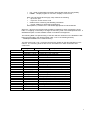
The following table is a specific listing of the files and their locations on the distribution disk.
Place the files listed in the following table under root in the following directory
PSDExpress\DK900-HC11\<table directory>
The files listed under root, are all the files that are needed for the demonstrations in this
manual. The remaining archives are source information from which these files were
constructed.
IAP
Demo
Hwtest
Root
Directory
Files
Dk9hciap_p_10.zip
Dk9hciap_c_10.zip
Readme.txt
Description
Full code bundle(c level code and psd files)
Contains all PSD source files
Contains all C level code files
Late breaking information
UART1-HC11.zip
Uart1.hex
Readme.txt
No psd or obj files
Contains all C level code files
Directly downloadable via IAP
Late breaking information
Dk9hchwt_p_10.zip
Dk9hchwt_c_10.zip
Readme.txt
hwt.obj
hwt.mmf
Full code bundle(c level code and psd files)
Contains all PSD source files
Contains all C level code files
Late breaking information
Duplicate obj file (also in PSD file above)
Memory map file used by PSDload
Iap_HC11.mmf
Iap_HC11.psd
Iap_HC11.obj
Uart1.hex
Memory map file(from PSDsoft project)
Configuration file for PSDload
Executing code for IAP demo
IAP demo file for direct download
5
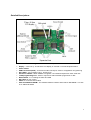
Detailed Descriptions
Figure 1 DK900-HC11 Development Board
•
•
•
•
•
•
•
•
•
•
Display - A two line by 16 character LCD display is included on the Development Board.
Power switch
UART Serial Port(male) - Connected to MCU serial port; used for In-Application Programming
HC11 MCU - Low cost MCU HC11, 44 pin PLCC
Socket for PSD9xx - Blank PSD9xx is supplied, user installs and performs initial JTAG ISP.
JTAG programming Port - Used in conjunction with FlashLINK programmer for ISP.
Reset Button - For resetting the MCU and PSD
DIP switch for IAP control
LEDs for functional annunciation
Pads for additional SRAM - The resident PSD9xx contains either 2KB or 8KB SRAM. This site
is for additional SRAM.
6
Step-By-Step Instructions for ISP Demo:
a) Locate and install PSDsoft Express and PSDload. The latest version is always on the web.
b) Plug the blank PSD9XX device into the Eval board socket.
c) Plug the FlashLINK Programmer into your PCs parallel port and plug in the ribbon cable to the
JTAG port on the eval board (for help see the Appendix C, FlashLINK manual).
d) Plug in power supply and turn on power. Typically you will observe that the top row of
characters are black boxes. This indicates no code is running on the board. You may need to
adjust the contrast control located on the left side of the board under the LCD.
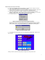
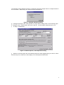
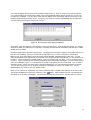
e) Run PSDsoft Express. Here is the initial screen if no project is open.
Figure 2 Opening screen upon PSDsoft Express invocation
Use cancel at this point since all we need to do is program the PSD and there is no need to
create a project. Later, in the Using the DK900-HC11 as a development platform section, a
further tutorial is given on using PSDsoft Express with the DK900-HC11 for development.
Figure 3 Invocation reminder screen
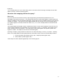
f) In the Design Flow (shown below), click on the Waferscale JTAG/ISP button. Bottom row of
boxes left side.
Figure 4 PSDsoft Express flow
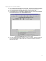
Clicking on this box yields the JTAG Operations- Single device dialog shown below.
7
The following screen appears inquiring if its desired to program a single device or multiple devices in
the JTAG chain. Select Only one as shown below and click OK.
Figure 5 JTAG-ISP Operations dialog
g) Clicking OK brings up the JTAG Operations Single Device dialog shown in the following figure.
h) Browse to the *.obj file shown, and click on this file. The information will be filled in for you.
i) In Step 2, click Execute.
Figure 6 PSDsoft Express, JTAG Operations dialog
j) Observe in the lower pane the JTAG activities that occur while programming your device. When
activities stop here, observe the LCD display on the Development Board itself.
8
k) When the download is completed the Development Board will boot automatically, showing the
displays below: This display will sequence one time, ending with the last screen, PSDload Test.
This is the screen that needs to be active for the following IAP demo.
D K
9 0 0
E v a l
C o n g r a t
I S P
w a s
h a t
s
I
i o n
s
D o w n l o a d
S u c e s s f u l
P l e a s e
p o w e r
t
t
I
u l a t
B d
n
c y c l e
o
s e e
p r o g r a m
f l a s h
T H A N K S
P S D l
o a d
T e s t
Figure 7 Eval Board Displays for ISP
If you power off/on the board, you will see that the display will resequence, confirming that the
program and all configuration information are stored in the PSD's non-volatile memory.
l) For better understanding of the program you may want to examine the following resources:
1. System memory map. Figure 18.
2. PSDsoft Express project
3. The file source code (included) to see the flow of the executing code
9
Step-By-Step Instructions for IAP Demo:
a) Now, let's perform an In-Application Programming (IAP). Disconnect the FlashLINK programmer
and close PSDsoft Express. Connect the serial cable to the serial port on the PC, and the Dsub
connector on the Development Board. Note that this cable is a null modem cable(F-F).
b) Once the Development Board displays PSDload Test, proceed to the next step.
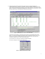
c) Invoke PSDload on the PC. At invocation of PSDload, most buttons will be greyed out indicating
the PC communications port is not configured as shown below.
Figure 8 Initial PSDload invocations screen (no comm)
d) From within PSDload, choose File, then Open. Find the file as follows; \DK900-HC11\iap\*.psd.
This is a configuration file for PSDload thats been constructed for this demo containing the
particulars of the design.
10
e) Observe the buttons become active(colorful) when this file is selected indicating the
communications port is configured. If the button colors do not appear, change the comm port
(while retaining 19.2Kbaud) using the Select, Communications submenu or the Comm Port hot
button. In this case, you will also be prompted for the *.mmf file from the same directory. Do not
leave this step until youve achieved active buttons as shown below.
Figure 9 Initial PSDload invocations screen (with comm)
As well as the active buttons, notice that the main window is now populated with the active
design. The entries are effectively the equations used to determine the memory map. This
information was entered in PSDsoft Express during the design phase of the project and
conveyed to PSDload via the *.psd file (mmf file derivative).
If you must use the *.mmf file, the following two dialogs will appear;
The first is to setup the communications parameters.
Figure 10 PSDload comm parameter dialog
11
The second is the Describe Memory Usage dialog box. Here the user is to declare how the PSD
memory is used as well as which me mory locations are unpopulated at the present time(ghosts).
The unpopulated locations occur from the desire to swap memory; in these cases there is
typically only one resident location for the memory at any particular time. The alternate location
also exists and is used after memory is swapped.
Figure 11 PSDload Describe Memory Usage dialog
f)
Now, do a Write To Display using the Action, Write Display submenu or the LCD Display hot key.
Type something in the dialog, press OK and see if it comes up on the Development Board
display. If it does, youve successfully established communications between the PC and
Development Board. If this doesnt work, check the following;
1. cable is plugged in
2. cable is of correct type(Null modem, F-F)
3. the correct comm port is selected on the PC
12
g) Select Action, download to observe the Download Segments dialog. The following screen will
appear.
Figure 12 Download Segments dialog, PSDload
Selecting the download destination (Step 1) to be fs7_a. Behind the scenes fs7_b will automatically
be selected as the execution location. This will be confirmed in the next screen. Click OK.
h) Now the Download Selection Summary screen, below, pops up. The intent is to validate the
settings chosen in the last screen. You should see fs7_a as the download destination and fs7_b
as the execution location. Click Download to start the process or back to change.
Figure 13 Download Summary screen
i)
Observe the progress bar at the bottom of the PSDload window for activity. Also, observe the
display on the Development Board as follows.
P S D l
d o w n l
o a d
o a d i
t e s t
n g
*
Figure 14 Development Board display for download in process
13
During the download, youll observe the * character position changing between the following -, \,
|, and /. A change from one character to the next occurs with each new packet received by the
Development Board. When the download is complete you will see the following.
P S D l
d o w n l
o a d
o a d
t e s t
d o n e
Figure 15 Eval Board display for download complete
Next, observe the results of the checksum calculation covering the entire downloaded contents
as shown below. Of course this was a successful download. This particular display does not
persist, so watch the display intently.
P S D l o a d
c h e c k s u m
t e s t
g o o d
Figure 16 Eval Board display for checksum validation
j)
On the Development Board, place SW-PB3 in the on(up) position. This switch is read when the
board boots and indicates to the software the desired execution location. On(up) indicates the
desire to execute from the main flash area which you just downloaded. Off(down) indicates the
desire to continue executing from the default boot area.
and observe the Development board display. The program you
k) Now click the reset button
just downloaded to the main flash area will boot showing the displays listed below.
Y o u
p e r f
h a v e
j
o r m e d
u s t
I n - A p p l i c a t i o n
P r o g r a m m I n g ( I A P )
T h e
d u r i
o f
a
i n t o
N o w
o f f
M C U
o p e r a t e d
n g
d o w n l o a d
n e w
t h e
p o w e r
c y c l
a n d
o n
t o
s e e
t h e
p r o g r a m
G O O D
p r o g r a m
F l a s h
n e w
e x e c u t
e
e
J O B !
Figure 17 Eval Board display sequence for In Application Programming(IAP)
You can cycle power or press the reset button again to see that this code also persists in non volatile
FLASH memory. Note that this code bundle contains less communications capability than the IAP
code run previously.
l)
Now, lets reinvoke the original program that was running prior to the IAP download. This is
done by placing SW-PB3 in the off(down) position. Now press the reset button and observe the
original, ISP program execute again.
14
Using DK900-HC11 as a Development Platform for HC11 MCU users:
Concept
The Waferscale DK900-HC11 Development Board provides the following capabilities
• Demonstrate design concepts early, optimizing time to market
• Jump start user application with proven framework (hardware and software)
• Substitute for user target system until target prototypes are available
• Gives instant platform for testing ISP and IAP demonstration.
• Allows programming the PSD using included Flashlink cable
General Board Description
The DK900-HC11 Development Board is specific to the HC11 microcontroller family. The board
contains an empty socket for the PSD9xx, which can be populated with the included PSD9xx family
component. Programming of the PSD is required since the component provided is blank.
Downloading to the Development Board
Executable code can be downloaded to the Development Board two different ways; via the JTAG
(ISP)or via the UART (IAP). Both methods are described and demonstrated in the Step by Step
demos for ISP and IAP earlier in this manual.
The ISP programming can program all elements within the PSD (PLD, MAIN FLASH, secondary
FLASH memory and all configuration elements) using the 2x7 JTAG connector. That is, all internal
PSD components can be programmed via this channel.
The IAP method uses a standard null modem PC serial cable (F-F) and PSDload PC software
downloaded from the web as well as the UART of the installed MCU. The IAP method allows only
data and executable code to be downloaded over a PC serial link. The PSD, PLD cannot be
updated by the IAP channel.
The IAP method is not restricted in destination to the PSD. The destination can be any resources on
the Board itself; PSD components or the external SRAM (SRAM not supplied, user must solder in
standard 32Kx8 SRAM if you desire more SRAM than is contained in the PSD).
PSDload, a win95/98/NT compatible application for the PC, administers the PC side of the serial link.
The protocol used is described in PSDstep document on the web.
JTAG - ISP
The PSD813F JTAG interface provides the capability of programming all memory within the PSD (
PLD, configuration, MAIN and secondary FLASH memory and BOOT areas ). This interface can
also be used to program a completely blank component as JTAG enabled is the default PSD state.
See Application Note 54 (AN054) for further description on our CD or website at
www.waferscale.com.
The LCD will be non operational during JTAG - ISP, since the MCU is not operating. During this
interval, the PSD is not connected to the MCU bus.
Waferscale provides a FlashLINK programmer to facilitate this JTAG programming operation. The
FlashLINK programmer connects the PC parallel port to the JTAG connector (2x7) and is driven by
PSDsoft Express, the PSD development tool.
15
PC Software
UART Support, PSDload
PSDload is a PC application (WIN95/98/NT) which allows serial communications between the PC
and the Waferscale's series of Development Boards. This application utilizes the microcontroller
UART on the target system side and a standard serial PC channel. The protocol utilizes commands
to perform the following functions on the resident PSD, and potentially, other Development Board
resources.
1. Read and write registers, memory
2. Erase and fill memory areas
3. Write to the LCD display
4. Download files from the PC to the target system(any system area)
5. Program the downloaded file into the PSD memory in circuit(MAIN or BOOT areas)
6. Upload files from the PSD or development board resources
7. Reset the target system.
The primary target of this interface is FLASH based PSDs from the standpoint of in circuit
programmability. However, the capability is also applicable to the OTP family of PSDs(note that in
circuit programming is not available due to the OTP families EPROM base).
Definition of Terms
A few term definitions will ease the understandability of the document.
a. PSDLoad is the windows interface running on the PC.
b. PSDStep is the protocol used to communicate between the PC and the Evaluation board.
(Simple Test and Evaluation Protocol).
Serial Interface
The connection from the PC to the evaluation board is via a standard 9 pin null modem cable(F-F).
The communications parameters are 8 data bits, 1 stop bit and no parity. The interface uses simple
three wire (TX, Rx and GND) RS-232 with full-duplex operations. Flow control is accomplishe d via
software handshaking incorporated into the protocol (this is not XON XOFF). The baud rate of
PSDload is selectable from 4.8k to 56k but the HC11 board is presently restricted to 19.2kbaud.
Software flow control is used in order to minimize the master/slave physical connections.
Each command sent from PSDload is intended to elicit a response from the Development Board.
This handshake is used to verify a valid receipt of the transaction. Two methods exist to terminate
this handshake if it should become disrupted for any reason; the first is a hot key inside PSDload,
and the second is a communications timeout parameter entered on comm invocation screen.
PSD Architecture
The PSD contains several different blocks of memory which vary within each family and between the
families. These encompass the following memory types; EPROM, FLASH, EEPROM, SRAM, and
registers. Generically these memory blocks are termed a memory region. The PSD913 contains
128kx8 FLASH, 32kx8 FLASH and 2kx8 sram.
PSDLoad must be aware of how these regions map into the system memory as all operations occur
based on addresses associated with the system memory. The system memory map is determined
using the development tool, PSDsoft Express. This information is provided in the form of a *.mmf file
automatically generated from PSDsoft Express and requested by PSDload at invocation. PSDload
utilizes this information to portray the system memory map to the user and construct commands to
send to the Eval Board. The *.psd file, once constructed, contains the information in the *.mmf file.
Since the system memory map is utilized to achieve the download, the PLD within the PSD must
have been programmed prior to a serial download attempt. PLD programming is accomplished via
16
either the JTAG interface or with a conventional parallel programmer, both of which are external to
PSDstep/PSDload.
Note that the addressing scheme used by PSDload is a different addressing scheme than is used by
PSDPro(parallel programmer) and/or FLASHlink. PSDload uses the system addresses; that is, the
addresses generated by the microcontroller in the system and correlated by the linker. PSDsoft
Express and FLASHlink use direct addresses (flat 24 bit memory space), that are independent of the
PLD and the end system application.
The FLASH region is erased by sector or bulk(entire FLASH) and programmed byte by byte. The
EEPROM region does not require erase and may be written by byte or by page. Which technology
resides in the BOOT area depends on the device you have chosen. For example, the F1 has
EEPROM in the BOOT area. An unambiguous method to determine the BOOT area technology is
by reading the flash ID.
Functions Available
Along with the standard windows controls of save
, open
, new
, close
and help
, the following are available. These functions are can be accessed
and the serial port controls
either from a pull down menu (Action) or from the shown hot keys.
Function
Description
Erase
Fill
Download
Upload
Read
Write memory
Write display
Reset board
User data
Source file entry
Describe memory usage
Erase FLASH(by segment or bulk)
Fill area
Download new file to memory
Upload file from memory
Read area(restricted to 160 bytes)
Write area(restricted to 160 bytes)
Write to display (on dev board)
Reset development board
Encapsulate user specific commands
Enter source file to be downloaded
User interface aid
Table 1 PSDload Commands
17
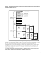
Memory Map
Before we really get started using PSDload, we should be familiar with the system memory map. Recall that
all PSDload operations occur by using addresses in this map. The applicat ion is set up to take advantage of
the entire memory space of the 9xx using paging techniques even though the MAIN FLASH is initially
unpopulated(fs0..7). CSIOP is the base of the register band used to communicate with the PSD using the
microcontroller.
FFFF
csboot1
68HC11 boots from the reset
vector stored here
8Kbytes
Secondary Flash
IAP loader code
gets programmed
here by JTAG-ISP
or a convetional
programmer tool.
csboot0
COMMON
REGION
(any page)
8Kbytes
Secondary Flash
C000
nothing mapped
A800
rs0, 2Kbytes SRAM
A000
nothing mapped
8400
8300
8200
8000
cs_lcd , ext chip sel for LCD
csiop, PSD control regs
68HC11 Regs/RAM
fs1
16Kbytes
Main Flash
PAGED
REGION
8000
fs3
16Kbytes
Main
Flash
8000
fs5
16Kbytes
Main
Flash
4000
8000
fs7
16Kbytes
Main
Flash
4000
fs0
16Kbytes
Main Flash
0000
fs2
16Kbytes
Main
Flash
PAGE 0
0000
csboot3
fs4
16Kbytes
Main
Flash
PAGE 1
0000
fs6
16Kbytes
Main
Flash
PAGE 2
0000
PAGE 3
0000
8Kbytes
Secondary
Flash
csboot2
8Kbytes
Secd Flash
PAGE 4
Figure 18 Memory Map of Eval Board
Getting started with PSDload
Since youve done this before in the previous step by step demo section, well start with PSDload being
active. To establish a baseline communications, write something to the display by selecting the Action
submenu and then Write Display. A dialog will pop up allowing you to enter text. After you have completed
the message, click on the Write button. PSDload will send out the message. After the message has been
received, the development board responds by displaying the message and sending a response back to
18
PSDload. This response prompts PSDload to display an operation completed dialog to the user on the PC.
All transactions between PSDload and the development board use this handshaking scheme to maintain
continuity of the communications link.
A few reads and writes
Now lets do a few read/write operations. We want to be careful in the selection of the address that were
writing to, so we wont interfere with the execution of the present application. Do a read memory of RS0 by
selecting RS0 in the Select Segment field. When you select RS0, the start address of 0xA000 is populated
in the start address field. Modify this field to 0xA700 for the purposes of this test and enter a length of 40h in
the Length field. The following figure shows the dialog prior to clicking OK. Click OK.
Figure 19 Read Memory dialog in PSDload
A dialog will pop up with the contents of the memory in both hex (left side) and asc formats(right side) as
shown below.
Figure 20 Read Memory Data in PSDload
19
The contents appear as zeros as this is initialized volatile memory. Now, do a write of the same locations.
Youll see the same box (read memory data) come up as PSDload always does a read prior to a write, but
now the box is editable. You can edit in either the hex display or the asc display and the conversion to hex
happens automatically as shown below. Try typing your name or something identifiable into the ASC field.
You will notice the hex bytes changing as you type.
Figure 21 Write Memory Data dialog in PSDload
Click Write. After the response, read it again to see if its really there. Cycle power and reread. You should
observe the data you entered is no longer there, indicating the fact that the information was stored in volatile
SRAM which is volatile.
Now lets repeat these operation using FLASH. The dialogs are the same except for the FLASH selection so
they wont be repeated. Since its not used in the application yet, no harm will be done. Select Write
Memory and, in the write dialog, select fs7 which stars at 0x0000. Read 40h bytes of the area. You will
notice that instead of the characters you observed in the above example using SRAM, you now get 0xff in all
locations. This is because the FLASH is blank. Type in something and click write. Now do a read to see if
its there. Type in something else of lesser length than above and read it back again. You will notice that the
entire first message is gone. This is because the FLASH was erased prior to the last write. Also, FLASH is
erased by sector; that is, the entire sector must be erased before you can rewrite the locations of interest.
You can also cycle power on the target to see that the information is held in non volatile form. Also try
ERASE which only works on the non volatile areas.
When youre ready to do a download, one of the operations thats needed is the selection of the source file.
button. After exiting this screen, the selected hex
This screen available from the Action submenu or the
file shows up in the main mmf display. The same file and path are stored in the *.psd file when its saved.
Figure 22 Hex File Selection screen, PSDload
20
Download
Youve already done this in the earlier demo portion of this document so lets dig a bit deeper to see what
makes it all work. See the following section.
How does this swapping stuff work anyway?
Macro level
First, lets take a look at how the memory map changes during the transitional operations from one
executable code bundle to the other. The internal PSD resource of the PAGE register is used to affect this
change in addition to the PLD equations described. We will also use a non volatile resource to carry through
a power off condition. This resource will be called NVswap and can consist of any of the following (spare
non volatile segment in the PSD, board level switch, etc). In our case, Nvswap will be the board mounted
DIP switch.
The PAGE register (csiop+0xE0, 8 bits) is traditionally used to control memory paging, but we also use it to
control memory addresses, as presented to the microcontroller, using 1 or more bits. This register can be
read or written by the microcontroller. The initial value of the PAGE register is 0 at power up and is the
register is volatile. The swap bit is the msb of the PAGE register.
Following is a step by step procedure to boot from one code and change, on the fly, to another. Certainly,
there is more setup detail involved (described later under Micro level), but this is the essential procedure.
1. Power up system with default memory map. swap=0 (PAGE register msb)
2. Write swap=1 (PAGE register msb)
These steps are further depicted graphically in the following figures.
21
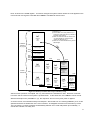
Heres the memory map at power up. Note that we are executing from CSBOOT0/1. During the IAP
download, the complete new executable, including the vector table, is copied into FS7. During this time the
swap bit in the PAGE register is 0.
FFFF
csboot1
68HC11 boots from the reset
vector stored here
8Kbytes
Secondary Flash
IAP loader code
gets programmed
here by JTAG-ISP
or a convetional
programmer tool.
csboot0
COMMON
REGION
(any page)
8Kbytes
Secondary Flash
C000
nothing mapped
A800
A000
rs0, 2Kbytes SRAM
nothing mapped
8400
8300
8200
8000
cs_lcd , ext chip sel for LCD
csiop, PSD control regs
68HC11 Regs/RAM
fs1
16Kbytes
Main Flash
PAGED
REGION
8000
fs3
16Kbytes
Main
Flash
8000
8000
fs5
fs7
16Kbytes
Main
Flash
16Kbytes
Main
Flash
4000
4000
fs0
16Kbytes
Main Flash
0000
fs2
16Kbytes
Main
Flash
PAGE 0
0000
csboot3
fs4
16Kbytes
Main
Flash
PAGE 1
0000
fs6
16Kbytes
Main
Flash
PAGE 2
0000
PAGE 3
0000
8Kbytes
Secondary
Flash
csboot2
8Kbytes
Secd Flash
PAGE 4
Figure 23 Memory map at power up, NVswap=0
Now, lets set a flag (NVswap) to indicate we want to run the code in FS7 the next time we power up. This
flag is non volatile so that, if power is removed, the system knows how its desired to power up.
Cycle power to the unit. We have embedded code running in the initialization routine to read the state of
NVswap and to write that value into the PAGE register (msb, swap) at power up. If swap= 0, the code
bundle residing in CSBOOT0/1 continues to run. If swap = 1, we perform the memory manipulations
depicted in the next figure.
For purposes of this example, lets assume NVswap = 1 indicating the desire to execute from the MAIN
FLASH memory. At this point, the code residing in CSBOOT0/1 is still running.
22
Next, we write to the PAGE register. This action changes the system location where the code appears to the
microcontroller moving FS7 to 0xC000 and CSBOOT to 0x4000 as shown below.
1) SWAP bit = 1.
2) Now the MCU boot area (C000-FFFF) is
occupied by main flash memory instead of
secondary flash memory.
3) MCU can download new IAP loader code
into csboot0/csboot1 if desired after
setting the UNLOCK bit = 1.
4) MCU can use csboot2/csboot3 for general
data storage.
FFFF
fs7
16Kbytes
Main
Flash
C000
AP
SW
COMMON
REGION
(any page)
nothing mapped
A800
A000
rs0, 2Kbytes SRAM
nothing mapped
8400
8300 cs_lcd, ext chip sel for LCD
csiop, PSD control regs
8200
68HC11 Regs/RAM
8000
8000
16Kbytes
Main Flash
fs3
16Kbytes
Main
Flash
fs5
16Kbytes
Main
Flash
4000
fs0
16Kbytes
Main Flash
0000
fs2
16Kbytes
Main
Flash
PAGE 0
0000
8000
csboot1
fs1
PAGED
REGION
8000
fs4
16Kbytes
Main
Flash
PAGE 1
0000
8Kbytes 2nd
Flash
If UNLOCK = 1
csboot1
8Kbytes 2nd
Flash
If UNLOCK = 1
csboot3
fs6
16Kbytes
Main
Flash
PAGE 2
0000
4000
PAGE 3
0000
8Kbytes
Secondary
Flash
csboot2
8Kbytes
Secd Flash
PAGE 4
Figure 24 Memory locations after step 3 of memory swap
After this write operation is complete, the very next instruction is fetched from FS7. Execution continues
from FS7 until the next time the system is powered down. At the same time, the CSBOOT area is moved.
With the NVswap bit set ( SW-PB3 on, up), this sequence will occur every time power is applied.
As a short review, lets talk about what just transpired. We booted from one memory(CSBOOT), then, at full
speed and without the awareness of the microcontroller, we swapped execution from that memory to FS7.
The new memory contents contained a substantially different set of code that picked up immediately. It
sounds like a stretch, but really isnt.
23
PSDload address translation
If you look closely at the memory map, you will observe that the system addresses are not the same for fs7
and csboot0/1. However, when these respective code bundles execute, they must occupy the same address
range. Else, the mcu could not find the reset vector, boot and execute the code.
More specifically, when a download occurs, the downloaded hexfile contains addresses appropriate for
execution that, in this case is 0xC000-0xFFFF for FS7. However, we download this data to 0x4000 7FFF.
If the downloaded addresses of the hex file start at 0xC000, how does the data get to 0x4000? Then, after
download is complete , how does the code get in high memory for execution? PSDload does an address
translation on every data byte in the hexfile; that is, it changes the addresses according to the download
destination of 0x4000-7FFF using the following equation.
Destination address = hex file address + destination base execution base.
For this HC11 family example, code exe(hex file) is 0xC123, dest base = 0x4000, exe base = 0xC000
Download destination = C123 + 4000 C000 = 0x4123
While this equation may look like overkill for this example, it allows transparent PSDload operation
regardless if the MCU boots from high memory(HC11) or low memory (8031).
Now that weve described this level of operation, lets take a bit closer look at the detailed sequence that
occurs between steps 1 and 2; that is, as the memory is physically swapped.
Micro level
You might ask how can this happen without knowledge of the microcontroller? You might be wondering how
can this all happen with the microcontroller running full speed? It all happens due to the chip select
decoding.
Here are the equations that control the memory map before, after and during the transition. For clarity well
only consider the segments of interest for this application which are FS7 and CSBOOT0/1. Certainly the
same techniques apply with paging when using the remaining FLASH segments.
CSBOOT0 = ((address >= ^hC000) & (address <= ^hDFFF) & !swap )
# ((address >= ^h4000) & (address >= ^h5FFF ) & swap );
CSBOOT1 = ((address >= ^hE000) & (address <= ^hFFFF) & !swap )
# ((address >= ^h6000) & (address >= ^h7FFF ) & swap );
FS7
=
((address >= ^h4000) & (address <= ^h7FFF) & !swap)
# ((address >= ^hC000) & (address <= ^hFFFF) & swap );
The above equation tells us that FS7 can show up in either of two places; 0x4000-0x7FFF or 0xC0000xFFFF. The choice of which location is used is based on the variable swap, a single bit in the PAGE
register. The swap bit is the most significant bit of the PAGE register (csiop+0xE0). The PAGE register is 0
at power up. So, if swap=0 at power up, then fs7 must appear at 4000-7FFF and CSBOOT0 is at C0000xDFFF and CSBOOT1 is at 0xE000-FFFF. In this case, code executes from CSBOOT0 and CSBOOT1 as
a default. See previous figure for a graphical representation.
24
After the memory contortions are completed swap=1. We end up with the memory map of Figure 24 with
FS7 at 0xC000 (execution position) and CSBOOT at 0x4000.
The location where the vector table is located is generally referred to as the execution location in this
document. That is, this is where code needs to reside so that the microcontroller can find it easily. This
method of hardware relocation is very convenient due to the integrated components within the PSD.
Alternative methods use software relocation to accomplish the same task.
As an overview, consider this. What the microcontroller needs from the memory is really pretty simple. The
memory needs to provide the sequential instructions for the task at hand. The microcontroller generates the
address and the memory provides the instruction. Then the microcontroller executes that instruction. This
occurs over and over again. If a jump needs to occur, the microcontroller provides a new address to the
memory. Same with a subroutine return, the microcontroller gets the return address from the stack.
What really happens
There is a subtlety involved in the transfer of execution described above. This subtlety is because the MCU
really doesnt know the source of the instruction bytes; boot area or main FLASH. All the MCU knows is that
valid instructions on valid address boundaries are presented on the bus when the MCU needs them. Then
the MCU executes the instruction and generates the next address. The key element involved is the
generation of the address by the MCU.
To understand this critical transfer of control, lets examine the instruction by instruction transition from one
memory to the other. After the reset signal is deasserted, the MCU is executing from the csboot area
normally. This continues until the swap bit is written, moving FS7 into the execution location (0xC0000xFFFF). At this same time, csboot area is moved to 0x4000-7FFF. At this point, the MCU is generating the
next address from the instruction received from the csboot area. However, the next instruction will come
from the FS7 area. This next instruction fetch must be appropriate to maintain the program flow. That is, the
next instruction must be received by the MCU on an instruction boundary and be appropriate for the program
flow. In addition, any issues with the stack and stack pointer must be resolved so program flow can continue
(subroutine return addresses, temporary variables, etc.).
The method weve used to ensure correct operation is to place identical code at identical locations in both
applications through the point of the swap. After the point of the swap, the code bundles can diverge without
problems.
25
A detailed look at the IAP example implementation
The previous example uses two code bundles; IAP_6811 and UART. The discussion will take the same
course as the previous demos and explain what occurs behind the scenes. Lets take a walk through the
critical code to see how it works.
Top level functional flow
Lets start with the top level flow. After the reset vector is fetched and executed the routine evl_init.c runs.
This is where the main action occurs (evl_init.c) that resides in both IAP_6811 and UART1 applications.
Evl_init.c contains a routine Run_Execution_Source that determines where execution resides. The flow of
this routine is listed below:
Read_dip switch
If (dip_switch = up)
Execution_Main
If (dip_switch = down)
Execution_Boot
Of course, the execution from main flash will only occur properly if appropriate code is resident in main flash.
For Main flash execution, the swap bit is written and execution continues in the main flash area.
Now, lets assume that we are executing from main flash (DIPSW-PB3 = up) and wish to revert to the original
code for execution. All we need to do is place DIPSW3-PB3 in the down position and hit the reset button.
The csboot0/1 code starts out, then evl_init.c runs, leaving the swap =0 resulting in executing remaining in
the boot area.
As you can observe from the above discussion, the manipulations at the top level to accomplish the
traditional boot loader function using hardware techniques are straightforward.
How to create your own app for UART Download
Typically, getting a single application to run is relatively straightforward since the linker (and user) ensure all
references are resolved when the executable file is created. Setting up your application for UART download
takes only a little more coordination between the two executable files; specifically in the area of code
placement and using the linker. Typically only minor code changes are required.
First, a quick review of what were trying to do. We are attempting to smoothly transition from one running
application to another. The microcontroller will initiate the action, but be substantially unaware of its
occurrence. We are going to accomplish this by manipulation of the code memory presented to the
microcontroller.
Certainly this will take some coordination between the two applications, but probably not as much as you
might initially think. To make things easier, well do this critical transition just after a system reset as
described in A detailed look at the IAP example implementation section earlier in this document. This reset
can be initiated either through software or hardware means based on the method(s) available in your system.
You can tailor the scheme as described earlier in this document, or utilize the key generic elements listed
below;
1. Startup routine placed identically in both applications(csrtsi.s)
2. Flag indicating desire to jump from BOOT memory to main memory. This is the variable
(NVswap= 1)described earlier in this document.
3. Method to tell system of desire to return from main memory to BOOT memory. This is the
variable (Nvswap=0) also.
When using a PSD, we recommend the use of our crtsi.s routine or an equivalent included in the code
bundles. The code placement issues are serviced in the *.lkf file also included in the code bundles.
26
The code content and positioning after the initialization code ( crtsi.s) need have no correlation between the
two applications. That is, the linker can be allowed to handle post initialization code without ill effects to the
desired swapping operation. This element eases the creation of compatible applications as the critical code
placement is handled by this single file.
27
References
IEEE Std 1149.1-1990 IEEE Test Access Port and Boundary Scan Architecture
PSDSoft Express User Manual
Flashlink User Manual
Application notes
AN054 JTAG Information
AN067 Design Turorial for 8032/PSD9XX
28
Appendix
29
Appendix A - Jumper configuration on DK900-HC11 eval board
9. PSDs power consumption measurement point (JP7)
Two pins of this jumper are already connected using copper trace. To measure PSDs power consumption, connect
DMM to these two pins after cutting pre-connected copper trace on PCB.
The measured PSDs current will be,
Icc = PSD Icc + PSD Ic (I/O ports) + MCU Bus leakage Ic
This measurement could be different from result of calculation according to formula in data sheet. To measure
correct value, make sure all of other terms should be zero.
10. PC1 TCK input option (JP8)
Default setting of this jumper is non-buffered
1
1-2 : direct connection to FlashLink TCK output
2-3 : buffered TCK output from HC14 on board
11. PSD SRAM Battery Vstby input to PC2 (JP9)
Default setting of this jumper is weakly pulled up (disabled Vstby input from battery)
1
1-2 : connect PC2 to battery on board
2-3 : PC2 is weakly pulled up through 100K ohm
30
12. SRAM (1M/256Kb) / STs TimerKeeper SRAM Expansion
(a) 0.3 pitch 256Kb SRAM expansion site (28PIN)
A14
A12
PA7 (A7)
PA6 (A6)
PA5 (A5)
PA4 (A4)
PA3 (A3)
PA2 (A2)
PA1 (A1)
PA0 (A0)
AD0
AD1
AD2
GND
A14
A12 /WE
A7
A6
A5
A4
A3 /OE
A2
A1 /CS
A0
D0
D1
D2
VCC
VCC
PB5 (/WR)
A 13 A13
A8 A8
A9 A9
A11 A11
PB4 (/RD)
A10 A10
PB6 (/RAM_CS)
D7 AD7
D6 AD6
D5 AD5
D4 AD4
D3 AD3
(b) 0.6 pitch 1Mb/256Kb SRAM or STs TimeKeeper SRAM expansion site (32PIN)
NC
PB1
A16
JP3 (A14) A14
A12
A12 /WE
PA7 (A7)
A7
PA6 (A6)
A6
PA5 (A5)
A5
PA4 (A4)
A4
PA3 (A3)
A3 /OE
PA2 (A2)
A2
PA1 (A1)
A1
PA0 (A0)
A0
AD0
D0
AD1
D1
AD2
D2
GND
A15
CS2
PB5
A13
A8
A9
A11
PB4
A10
CS1
D7
D6
D5
D4
D3
VCC
PB0
JP1 (VCC)
(/WR)
JP2 (A13)
A8
A9
A11
(/RD)
A10
PB6 (/RAM_CS)
AD7
AD6
AD5
AD4
AD3
*) PB0, 1 can be used for banked SRAM
(c) Jumper settings for 0.6 pitch devices
JP1
JP2
JP3
256Kb
SRAM
1Mb
SRAM
ST
M48T59
ST
M48T129
ON ( VCC )
ON ( A13 )
ON ( A14 )
ON ( CS2-VCC )
ON ( A13 )
ON ( A14 )
ON ( VCC )
OFF ( /IRQ/FT)
OFF ( /RST )
OFF ( /IRQ/FT )
ON ( A13 )
ON ( A14 )
*) Default : All JP1-3 are OFF
31
13. System expansion connectors (J1,J2,J3)
J1 (68HC11Dx)
1
2
GND
AD0
AD1
AD2
AD3
AD4
AD5
AD
AD7
/XIRQ
R_W
AS
/RESET
/IRQ
PD0
PD1
PD2
PD3
PD4
PD5
J3 1
E
MODA
MODB
A8
A9
A10
A11
A12
A13
A14
A15
PA0
PA1
PA2
PA3
PA5
PA7
JP4 (VCC)
2
1
2
J2 (PSD8/9xx)
PA0
PA2
PA4
PA6
GND
PB0
PB2
PB4
PB6
GND
PC0
PC2
PC4
PC6
CNTL2
PD1
PA1
PA3
PA5
PA7
GND
PB1
PB3
PB5
PB7
GND
PC1
PC3
PC5
PC7
/JEN
PD2
* /JEN is connected to
FlashLink
* JP4 is OPEN as
default.
PA4
PA5
14. Others
(a) Battery power connector and re-charging circuit
When using re-chargeable battery as power source, you can use prepared normal charging circuit in this kit. To
use this charging circuit, assemble a diode with register that has proper value.
(Recommended battery is NiCD 10.8V)
*) Do not use charging circuit for Manganese, Lithium or Hydrargyrum batteries.
(b) Other power source input connector
To use other power sources (SMPS, Transformer,
), a connector is prepared in this kit.
(Recommended power source is AC/DC adapter, over 9V, output can be AC or DC)
(c) Re-charging circuit for Vstby Battery
When using re-chargeable battery as Vstby source, you can use prepared normal charging circuit in this kit. To
use this charging circuit, assemble a diode with register that has proper value.
(Recommended battery is NiCD 3.6V)
*) Do not use charging circuit for Manganese, Lithium or Hydrargyrum batteries.
.
32
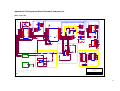
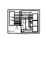
Appendix B Development Board Schematic and parts list
Main Schematic
C1
RP7 (*)
2
3
4
5
6
7
8
9
22pF
R1
10M
VCC
Y1
9.83MHz
1
VCC
C2
104M
22pF
/IRQ
/XIRQ
14
15
11
PPA0
PPA1
PPA2
PPA3
PPA4
PPA5
PPA6
PPA7
30
29
28
27
26
25
24
23
PPD0
PPD1
PPD2
PPD3
PPD4
PPD5
16
17
18
19
20
21
1
XT
EX
RESET
IRQ
XIRQ
PA0
PA1
PA2
PA3
PA4
PA5
PA6
PA7
PD0/RXD
PD1/TXD
PD2/MSO
PD3/MOSI
PD4/SCK
PD5/SS
PB0/A8
PB1/A9
PB2/A10
PB3/A11
PB4/A12
PB5/A13
PB6/A14
PB7/A15
PC0/AD0
PC1/AD1
PC2/AD2
PC3/AD3
PC4/AD4
PC5/AD5
PC6/AD6
PC7/AD7
E
AS
R/W
MODA
MODB
EVSS
(Note)
Rcharge = (5-3.6-0.6) /
(Ibat *charge%)
VCC
104M
Vstby
100K
U2
44
43
A8
A9
A10
A11
A12
A13
A14
A15
39
38
37
36
35
34
33
32
A8
A9
A10
A11
A12
A13
A14
A15
3
4
5
6
7
8
9
10
AD0
AD1
AD2
AD3
AD4
AD5
AD6
AD7
42
13
12
E
AS
R_W
41
40
MODA
MODB
AD0
AD1
AD2
AD3
AD4
AD5
AD6
AD7
2
3
4
5
6
7
8
9
RP6(*)
U1
1
VCC
100K
30
31
32
33
34
35
36
37
A8
A9
A10
A11
A12
A13
A14
A15
39
40
41
42
43
44
45
46
47
50
2
3
4
5
68HC11D0
AD0
AD1
AD2
AD3
AD4
AD5
AD6
AD7
1
VCC
RP5
4.7K
CNTL2
49
PD1
PD2
10
9
8
D1
AD0/A0
AD1/A1
AD2/A2
AD3/A3
AD4/A4
AD5/A5
AD6/A6
AD7/A7
PA0
PA1
PA2
PA3
PA4
PA5
PA6
PA7
A8
A9
A10
A11
A12
A13
A14
A15
PB0
PB1
PB2
PB3
PB4
PB5
PB6
PB7
(TMS)PC0
(TCK)PC1
(VSTBY)PC2
(TSTAT,RDY/BSY)PC3
(TERR,VBATON)PC4
(TDI)PC5
(TDO)PC6
PC7
CNTL0(R_W)
CNTL1(E)
CNTL2
PD0(AS)
PD1
PD2
48
29
28
27
25
24
23
22
21
PA0
PA1
PA2
PA3
PA4
PA5
PA6
PA7
7
6
5
4
3
2
52
51
PB0
PB1
PB2
PB3
/RD
/WR
/RAM_CS
LCD_E
20
19
18
17
14
13
12
11
TMS
TCK
Vstby
TSTAT
/TERR
TDI
TDO
PC7
VCC
(*)
R2
(*)
U3
RP1
1
(*)
D2
VCC
1N4148
Rcharge
1N4148
(*)
J4
1
2
(*)
BT1
3.6V
JP9
Vstby
2
3
4
5
6
7
8
9
PA0
PA1
PA2
PA3
PA4
PA5
PA6
PA7
2
3
4
5
6
7
8
9
PB0
PB1
PB2
PB3
/RD
/WR
/RAM_CS
LCD_E
100K
RP2
CON2
VCC
1
2
3
4
5
6
7
8
9
RP3
A0
A1
A2
A3
A4
A5
A6
A7
A8
A9
A10
A11
A12
A13
A14
A15
A16
D0
D1
D2
D3
D4
D5
D6
D7
CS1
CS2
WE
OE
13
14
15
17
18
19
20
21
AD0
AD1
AD2
AD3
AD4
AD5
AD6
AD7
22
30
29
24
/RAM_CS
JP1
/WR
/RD
VCC
628128
RAM EXPANSION
SW1
1
VCC
1
2
3
4
8
7
6
5
JP3
JUMPER
PB0
PB1
PB2
PB3
104M
(*)
100K
PB2
R?
(*)
560
LCD1
(*)
LED-PB2
LED
D7
D6
D5
D4
D3
D2
D1
D0
PB3
RP4
R?
560 (*)
VCC
(*)
LED-PB3
LED
1
U3D
R?
47
R-SIP5
8
9
VCC
GND
2
VCC
E
RS
R/W
VCC
VL
LCD MODULE
74HC14
14
13
12
11
10
9
8
7
AD7
AD6
AD5
AD4
AD3
AD2
AD1
AD0
6
4
5
LCD_E
PA0
R_W
3
R5
10K
1
104M
RA1C
100K
4
JP8
TCK-OP
A14
JP1
JUMPER
VCC
VCC
A9
JP2
JUMPER
SW DIP-4
PSD813FXPLCC
1
PB0
PB1
12
11
10
9
8
7
6
5
27
26
23
25
4
28
3
31
2
100K
RESET
2
3
4
5
PA0
PA1
PA2
PA3
PA4
PA5
PA6
PA7
A8
JP3
A10
A11
A12
JP2
1
VCC
Serial
TxD
RxD
R8
4.7K
(*)
D7
U3B
3
RESOUT
1N4148
74HC14
VCC
1
U5
VCC
VCC
JP7
GND
KIA7045P
3
U3A
2
C3
2.2uF/6.3V
11
VCC
/JEN
104M
10
74HC14
AD0
AD1
AD2
AD3
AD4
AD5
AD6
AD7
/XIRQ
R_W
AS
/RES
/IRQ
PPD0
PPD1
PPD2
PPD3
PPD4
PPD5
(*)
J1
1
3
5
7
9
11
13
15
17
19
21
23
25
27
29
31
33
35
37
39
2
4
6
8
10
12
14
16
18
20
22
24
26
28
30
32
34
36
38
40
PA0
PA2
PA4
PA6
E
MODA
MODB
A8
A9
A10
A11
A12
A13
A14
A15
PPA0
PPA1
PPA2
PPA3
PPA5
PPA7
PB0
PB2
/RD
/RAM_CS
TMS
Vstby
/TERR
TDO
CNTL2
PD1
2
4
2
4
6
8
10
12
14
16
18
20
22
24
26
28
30
32
PA1
PA3
PA5
PA7
PB1
PB3
/WR
LCD_E
TCK
TSTAT
TDI
PC7
/JEN
PD2
PPA4
PPA6
EXPANSION
CON4A
C5
0.1uF
(*)
J2
1
3
5
7
9
11
13
15
17
19
21
23
25
27
29
31
CON32A
JP4
JUMPER
VCC
1
3
PSD_Icc
C4
100uF/6.3V
13
11
9
7
5
3
1
(*)
J3
VOUT
+
14
12
10
8
6
4
2
CON40A
JTAG
74HC14
+
VDD
U3E
J4
CON14A
R2
470
1
S2
SW
74HC14
VCC
R10
4.7K
RA1C
100K
RST
2
13
D4
LED
1N4148
4
1
Power
12
4
74HC14
SER232.SCH
U3F
D7
5
2
U3C
6
/RES
RA1A
100K
RESET
PWRBAT.SCH
WSI ASIA Design Center
Rm. 401, Sung Woo Bldg., 15-12, Yoido-Dong
Youngdeungpo-Gu, Seoul, Korea
TEL: 82-2-761-1281 /2
FAX: 82-2-761-1283
JP1-4 are soldering jumper on solder side
(*) - not inserted
Factory setting using copper trace on board
Title
{Title}
Size
C
Document Number
{Doc}
Date:
Wednesday, April 19, 2000
Rev
{RevCode}
Sheet
1
of
5
33
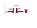
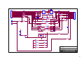
Serial Port Schematic
VCC
C7
+
1uF/16V
+
1
+
1uF/16V
3
4
+
C10
1uF/16V
TxD
RxD
RESOUT
5
11
12
10
9
U7
C1+
C1C2+
V+
V-
C2TI1
RO1
TO1
RI1
TI2
RO2
TO2
RI2
MAX232C
R5
2
6
10K
+
C9
14
13
7
8
C8
1uF/16V
C6
1uF/16V
5
9
4
8
3
7
2
6
1
P1
CONNECTOR DB9
34
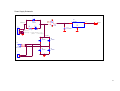
Power Supply Schematic
(*)
D9
1N4001
1
2
3
4
CON4
(*)
R6
Rcharge
S3
SW
(*)
D10
+
1N4148
(Note)
Rcharge =(Vdc-Vbat-0.6)/
(Ibat * charge%)
VIN
VOUT
2
VOUT
GND
(*)
J7
1
C11
470uF/25V
3
Vbat
U8
LM7805
Vdc
D5
1N4001
D6
1N4001
D8
1N4001
D7
1N4001
J6
DC JACK
(*)
2
1
CON2
35
Eval Board Parts List
No.
1
2
3
4
5
6
7
8
9
10
11
12
13
14
15
16
17
18
19
20
21
22
23
24
25
26
27
28
29
30
31
32
33
34
35
36
37
38
39
40
41
description
part number Q'ty
MCU
68HC11D0
0
PLCC socket
44P-PLCC
1
PLCC socket
52P-PLCC
1
5V regulator
KIA7805P
1
Reset comparator
KIA7045P
1
TTL
MC74HC14AN 1
232 Driver
ICL232CPE
1
Crystal
9,8304MHz
1
block resister array
AR100K-09P
3
block resister array
AR100K-05P
2
block resister array
AR4K7-05P
1
resister
10M 1/8W
1
resister
10K 1/8W
1
resister
4.7K 1/8W
2
resister
560 1/8W
3
resister
47 1/8W
1
potentiometer
GF06S10K
1
diode (switching)
1N 4148RL
1
diode (rectifier)
1N 4002RL
4
electrolytic capacitor 1uF/50V
EC1U50V
5
electrolytic capacitor 2.2uF/16V
EC2.2U16V
1
electrolytic capacitor 470uF/16V
EC470U16V
1
electrolytic capacitor 100uF/6.3V
EC100U6.3V
1
ceramic capacitor 22pF
CC22
2
monolytic capacitor 0.1uF/50V
M104
5
LED (green, 3mm)
BL-B2141-3D
3
4 position dip switch
KSD04H
1
power switch (slide 3P)
1
reset siwtch
1
SIP 2 pin header
1
SIP 14 pin header (LCD side)
1
SIP 14 pin connector (PCB side)
1
DB-9 connector
DB-9SR
1
DC-JACK
1
7x2 pin ribbon cable w/ male con. (150mm)
1
7x2 pin connector (angle)
1
standoffs (3 mm x 10 mm) for LCD
2
bolt,nut (2.6 mm x 16mm) for LCD
2
anti-static bag (170 mm x 300 mm)
1
box (110 mm x 150 mm x 24 mm)
1
LCD module
1
42 standoffs for PCB board
43 PCB board
4
36
Appendix C: FlashLINK Users Manual
Features
•
•
•
•
•
•
•
•
•
Allows PC parallel port to communicate with PSD9xx via PSDsoft Express
Provides interface medium for JTAG communications
Supports basic IEEE 1149.1 JTAG signals (TCK, TMS, TDI, TDO)
Supports additional signals to enhance download speed (!TERR, TSTAT)
Can be used for programming and/or testing
Wide power supply range of 2.7 to 5.5v
Pinout independent with target side flying leads
Convenient desktop packaging allows varying applications(desk, lab or production)
Synchronous JTAG interface allows speeds as fast as pc can drive
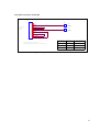
Overview
Flashlink is a hardware interface from a standard PC parallel port to one or more PSD9xx devices located
within a target PC board as shown below. This interface cable allows the PSD to be exercised for purposes
of programming and/or testing. PSDsoft Express is the source for driving FlashLINK.
Flying lead
cable
Mates with
PC parallel
port
12 WIRES
FlashLink
adapter
Target
device
6 feet
6 inches
Figure 25 Typical FLASHlink application
Operating considerations
Operating power for FlashLINK is derived from the target system in the range of 2.7 to 5.5 v.
Compatibility over this voltage range is ensured by the design of FlashLINK. No settings are involved.
On a cautionary note, it is recommended that the target system be powered with a well regulated and stable
source of power which is energized at the final value of Vcc. It is not recommended that the input voltage
be varied using the verneer on a regulated power supply, as this may cause the internal FlashLINK ICs
(74VHC240) to misoperate toward the lower end of the supply range.
Each FLASHLink is packaged with a six-inch "flying lead" cable for maximum adaptability (a ribbon cable
requires the use a certain connector on the target assembly). This flying lead cable mates to the FlashLink
adapter on one end and has loose sockets on the other end to slide onto 0.025 square posts on the target
assembly.
37
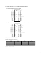
PIN
#
SIGNAL
NAME
1
2
3
4
5
6
7
8
9
10
11
12
13
14
JEN\
TRST\ *
GND
CNTL *
TDI
TSTAT
Vcc
RST\
TMS
GND
TCK
GND
TDO
TERR\
DESCRIPTION
JTAG = IEEE 1149.1
EJTAG = WSi EHANCED JTAG
Enables JTAG pins on PSD8XXF (optional)
JTAG reset on target (optional per 1149.1)
Signal ground
Generic control signal, (optional)
JTAG serial data input
EJTAG programming status (optional)
VDC Source from target (2.7 - 5.5 VDC)
Target system reset (recommended)
JTAG mode select
Signal ground
JTAG clock
Signal ground
JTAG serial data output
EJTAG programming error (optional)
Type
Flashlink
Signal
OC,100K
OC,10K
Source
Source
OC,100K
Source
Source
Destination
OC,10K
Source
Source
is
Source
Destination
Destination
Notes
1. Bold signals are required connections
2. all signal grounds are connected inside FlashLink adapter
3. OC = open collector, pulled-up to Vcc inside FlashLink adapter
4. * = Not supported initially by PSDsoft.
5. The target device must supply Vcc to the FlashLink Adapter (2.7 to 5.5 VDC, 15mA
max @ 5.5V).
Figure 26 Pin descriptions for FlashLink adapter assembly
All 14 signals may not be needed for a given application. Here's how they break down:
(6) Core signals that must be connected: TDI, TDO, TMS, TCK, Vcc, GND
(2) Optional signals for enhanced ISP (Option 3 flow control): TSTAT, TERR\
(1) Optional signal to control multiplexing of the JTAG signals: JEN\
(1) Recommended signal to allow FlashLink to reset target system during and
after ISP: RST\
(1) Optional IEEE-1149.1 signal for JTAG chain reset: TRST\
(1) Optional generic control signal from FlashLink to target system: CNTL
(2) Two additional ground lines to help reduce EMI if a ribbon cable is used.
These ground lines "sandwich" the TCK signal in the ribbon cable. These
lines are not needed for use with the flying lead cable, that is why the
flying lead cable has only 12 of 14 wires populated.
38
FLASHlink pinouts
There is no "standard" JTAG connector. Each manufacturer differs. WSi has a specific connector and
pinout for the FlashLink programmer adapter. The connector scheme on the FlashLink adapter can accept a
standard 14 pin ribbon connector (2 rows of 7 pins on 0.1" centers, standard keying) or any other user
specific connector that can slide onto 0.025" square posts. The pinout for the FlashLink adapter connector
is shown in figure 4.
A standard ribbon cable is good way to quickly connect to the target circuit board. If a ribbon cable is used,
then the receiving connector on the target system should be the same connector type with the same pinout
as the FlashLink adapter shown in Figure 4. Keep in mind that the JTAG signal TDI is sourced from the
FlashLink adapter and should be routed on the target circuit card so that it connects to the TDI input pin of
the PSD device. Although the name "TDI" infers "Data In" by convention, it is an output from FlashLink
and an input to the PSD device. Also keep in mind that the JTAG signal TDO is an input received by the
FlashLink adapter and is sourced by the PSD device on the TDO output pin. Use Figures 1, 2, 3, and 6 as a
guide.
WSi ENHANCED JTAG ISP CONNECTOR DEFINITION
14
VIEW: LOOKING INTO FACE OF
SHROUDED MALE CONNECTOR.
0.025" POSTS ON 0.1" CENTERS.
13
TERR TDO
12
Connector reference: Molex 70247-1401
11
GND TCK
9
10
GND TMS
8
7
RST
VCC
6
5
TSTAT TDI
3
4
CNTL GND
2
1
TRST JEN
Figure 27
KEY
WAY
Recommended ribbon cable for quick
connection of FlashLink adapter to end
product:
Samtec: HCSD-07-D-06.00-01-S-N
or
Digikey: M3CCK-14065-ND
Note:
TDI is a signal source on the Flashlink
and a signal destination on the target
board.
TDO is a signal destination on the
FlashLink and a signal source on the
target board.
Pinout for FlashLink Adapter and Target System
39
Target System, 3v or 5v
FlashLink
Adapter
Conncetor
Vcc
7
Vcc 7
9
TMS
TCK 11
9
TDI 5
5
TSTAT 6
!TERR 14
recommended
buffering
11
optional
optional
TDO 13
TMS
TCK
TDI
TDO
6
14
TSTAT
TERR\
PSD8XXF
13
!JEN 1 optional
2 optional
!TRST
3
GND*
4 optional
CNTL
8 recommended
!RST
GND* 10
GND* 12
1
2
3
4
8
10
12
TMS
TCK
Any JTAG
Device in
ByPass Mode
TMS
TCK
JTAG Chaining Example,
PSD8XXF and other JTAG
compatible devices.
2
TDI
TDO
* all ground pins are
connected together inside
flashlink assembly
straight through
ribbon cable
2 row, 7 position
1
n
TDI
TDO
System
Reset
Circuitry
TSTAT
TERR\
PSD8XXF
Figure 28 JTAG Chaining Example
40
SOLDERING PAD PATTERN
CBL1
D0(TCK) DB2
1
D1(TMS) DB3
2
D2(TDI) DB4
3
D3(JEN\) DB5
4
D4(TRST)
DB6
5
D5(RST) DB7
6
GND
DB18
7
ACKN DB10
8
PAP
DB12
9
ERRN DB15
10
SEL
DB13
11
BUSY DB11
12
D6
DB8
13
AUTO LINE FEEDDB14
14
red
org
pink
yellow
green
lt green
47
R1
47
R3
47
R5
grey
black
orgt
brnt
white
47
R7
47
R9
47
47
R2
47
R4
2
4
6
8
47
R6
1
47
R8
R11
47
U1A
A1
A2
A3
A4
100pf 100pf
C53 C54
R42
4.7K
100pf
C55
S1
1
PAD1
(FRAME GND)
0
R80
470K
10K
U2A
2
9
74AC05
U2B
3
G
/JEN
TRSTN
47
R17
CONTROL
TDI
TSTATN
VCCIN
RSTN
TMS
GND
TCK
GND
TDO
TERRN
47
R18
R19
R20
47
R21
10K
R22
10K
R23
P1
1
2
3
4
5
6
7
8
9
10
11
12
13
14
70247-1401
MOLEX
100K
R34
4
R30
74AC05
R43
4.7K
U3C
6
8
9
C25
5
74AC05
U3E
74AC05
0.01UF
R15
6
U3D
10
11
74AC05
VCC
(FOR U2)
4148
R13
47
47
10K
D2
47
4
3
VCC
R16
8
VCC
R28
4.7K
R14
47
74AC05
74AC05
5
R29
4.7K
R12
47
U2D
74AC05 U3B
SHIELD
(DRAIN WIRE)
47
47
U2C
10K
3
5
7
9
74VHC240
1
R25
Y4
Y3
Y2
Y1
R39
100pf
100pf 100pf
C56
C57 C58
R26
1
A4
A3
A2
A1
19
VCC
VCC
U1B
17
15
13
11
G
R10
VCC
PAD1
18
16
14
12
Y1
Y2
Y3
Y4
C24
74VHC240
100pf
C52
PAD14
S2
(FOR U1)
0.01UF
VCC
100K
R31
100K
R32
100K
R33
0.01UF
D4
1N5817
C26
VCC
(FOR U3)
R50
10
D3
4148
2
R41 4.7K
R40
10K
3
Q1
2N3904
C50
1UF
1
D1
6.2V
C51
0.01UF
R51
100K
0
R81
U3A
1
2
10K
R35
10K
R36
10K
R37
10K
R38
U2E 74AC05
11
10
74AC05
U2F
13
12
74AC05
U3F
13
12
74AC05
Waferscale Integration
47280 Kato Road
Fremont, CA 94538
Title
FlashLink Schematic
Size
B
Document Number
FlashLink PCB
Date:
Monday, July 26, 1999
Rev
G1
Sheet
1
of
1
41
Loop back connector schematic
J1
to flash
link
assy
1
2
3
4
5
6
7
8
9
10
11
12
13
14
J2
GND
1
TDI
!TSTAT
VCC
J1
1
GND
CON2
VCC
CON1
TMS
TCK
TDO
!TERR
CON14
14 pin dual row 0.025 sq
receptacle(polarized, same as cable 5)
PC output
signal
PC intput
signal
PC connector
line
TDI
!TSTAT
ACKN (8)
TMS
!TERR
ERRN (10)
TCK
!TDO
PAP (9)
Figure 29 Loop Back Tester, Passive, FLASHlink
42
Appendix D crtsi.s routine
;
;
;
;
;
;
crtsi.s
C STARTUP FOR MC68HC11
WITH AUTOMATIC DATA INITIALISATION
Copyright (c) 1995 by COSMIC Software
xdef_exit, __stext
xref _main, __memory, __idesc__, __stack
xref _evl_optn
switch .bss
__sbss:
svx:
dc.w
0
sve:
dc.w
0
;
switch .text
__stext:
ldx #__idesc__ ; descriptor address
ldy 0,x
; start address of prom data
inx
; skip address
inx
ibcl:
ldaa 0,x
; test flag byte
beq zbss
; no more segment
bpl nobk
; skip bank
inx
; info
inx
; if any
nobk:
stx svx
; save pointer
ldd 3,x
; end address
std sve
; in memory
ldx 1,x
; destination address
dbcl:
ldab 0,y
; copy from prom
stab 0,x
; to ram
inx
; next byte
iny
cpy sve
; last one ?
bne dbcl
; no, loop again
ldx svx
; reload pointer to desc
ldab #5
; size of one entry
abx
; point to next entry
bra ibcl
; and loop
zbss:
ldx #__sbss
; start of bss
bra loop
; start loop
zbcl:
staa 0,x
; clear byte
inx
; next byte
loop:
cpx #__memory ; up to the end
bne zbcl
; and loop
lds #__stack; re-initialize stack pointer
jsr _main
; execute main
_exit:
43
bra _exit
; and stay here
;
; Special routines for non-stop concurrnet swap & execute
; both boot and main code must have identical following routines
;
xdef _EXECUTE_SOURCE
xdef _Execute_Main, _Execute_Boot, _Return_Boot
xref _PSD8xx_reg
xref _PSDload_init, _PSDload
;
switch .text
;
; swap to main flash and execute main code
;
_Execute_Main:
cli
; disable all interrupts
ldaa #$80
ldy #_PSD8xx_reg
oraa $E0,y
; set SWAP in PAGE to 1
staa $E0,y
; now in main flash
jmp __stext
; jump to Cstarup of main
; hc11 option setting is not allowed
;
; swap to boot flash and execute boot code
;
_Execute_Boot:
cli
; disable all interrupts
ldaa #$7F
ldy #_PSD8xx_reg
anda
$E0,y
; clear SWAP in PAGE to 0
staa $E0,y
; now in boot flash
jmp __stext
; jump to Cstarup of boot
; hc11 option setting is not allowed
;
; swap to boot flash and execute PSDload with message in boot
;
_Return_Boot:
cli
; disable all interrupts
ldaa #$7F
ldy #_PSD8xx_reg
anda
$E0,y
; clear SWAP in PAGE to 0
staa $E0,y
; now in boot flash
lds #__stack
; initialize stack pointer before
; calling PSDload subroutine(s) written in C
jsr _PSDload_init
jsr _PSDload
; loop forever in C
;
_EXECUTE_SOURCE:
dc.b 'PSDload'
dc.b 'V1.0',0
end
44
Appendix E evl_init.c routine
void evl_init(void)
{
psd_init();
}
// initialize PSD
// if any PSD port(s) is/are used for
// latched address output for external data memory,
// the PSD port must be initialized in "evl_optn.c"
// to guarantee initialization of data segment.
Run_Execution_Source();
// check & run execution source
// EXECUTE_SOURCE[] containes this information
PSDload_init();
// initialize other I/Os for PSDload function
// This is for checking setting of execution source and running
extern void Execute_Main(void);
// to ensure, same code in both BOOT and MAIN
extern void Return_Boot(void);
// these functions are in Cstartup(crtsi.s)
extern void Execute_Boot(void);
extern const char EXECUTE_SOURCE[];
// this data storage also in Cstartup(crtsi.s)
void Run_Execution_Source(void)
{
char *copy_loc;
}
if (!read_dipsw(DIP_SW3)) {
// current execution location is BOOT
// && same Cstartup code may be in MAIN
copy_loc = (char *)(((uint)EXECUTE_SOURCE - boot_mem_start_addr) + unswapped_Fseg_addr);
page_set (unswapped_Fseg_page);
if ( !page_get(SWAP) && !strcmp(EXECUTE_SOURCE, copy_loc) )
Execute_Main();
}
else
// current execution location is MAIN
// && execution source setting is BOOT
if ( page_get(SWAP) )
Execute_Boot();
// This is initialization for only direct PSDload running
// this can be called from STARTUP.A51
void PSDload_init(void)
{
com_initialize();
// initialize UART buffer.
init_message_level();
// initialize message level variables
timer_initialize();
// initialize real time interrupt,
lcd_init();
}
// initialize LCD. 8 bits, 2 lines, 5x7 font,
// no blink, cursor off, clear
45