1
MOTOROLA
SEMICONDUCTOR TECHNICAL DATA
AN781A
MOTOROLA LONWORKS TECHNOLOGY
AN781A
AL–3
AN781A
AL–4
MOTOROLA LONWORKS TECHNOLOGY
MOTOROLA LONWORKS TECHNOLOGY
AN781A
AL–5
AN781A
AL–6
MOTOROLA LONWORKS TECHNOLOGY
MOTOROLA LONWORKS TECHNOLOGY
AN781A
AL–7
AN781A
AL–8
MOTOROLA LONWORKS TECHNOLOGY
SEMICONDUCTOR TECHNICAL DATA
R
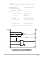
mode, the Neuron Chip can initiate and establish
synchronization with the slave. The slave must be either a
Neuron Chip configured in slave A mode or a foreign
processor emulating slave A mode.
A Neuron Chip in slave A mode implements a hardwired
handshake line (HS). The HS line and data are available in
the same clock cycles. Although this mode was designed to
interface with a Neuron Chip master, either a foreign
processor or another Neuron Chip can act as the master.
See Figures 2a and 2b.
The Neuron Chip slave B mode is logically similar in
operation to the slave A mode; however, the handshake is
read from the slave’s control register in one cycle and the
data is available in a separate cycle. The slave B mode was
designed to make the Neuron Chip act like a peripheral
device on a non–Neuron address bus. The master must be a
foreign processor as the Neuron Chip master mode is
designed to interface to a slave A configuration. See
Figure 2d.
The Neuron C programming language provides several
built–in functions that enable the use of the parallel I/O object
without the need for a detailed, hardware–level knowledge of
the handshaking protocol. These functions are discussed in
detail in the Neuron Chip–to–Neuron Chip interface section
of this document.
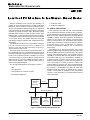
INTRODUCTION
This application note describes the parallel I/O object of
the MC143150 and MC143120 Neuron Chips, including
specifics on the handshaking and token passing process
used to establish synchronization and prevent bus
contention. Examples are provided for interfacing to both a
foreign processor (non–Neuron microprocessor or
microcontroller) and other Neuron Chips. Timing, interrupts,
and memory allocation are also discussed.
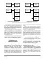
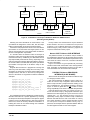
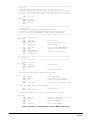
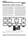
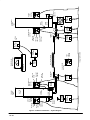
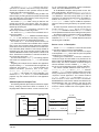
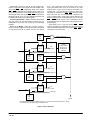
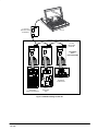
Utilizing this application, the Neuron Chip can act as a
communication chip for the foreign processor or can create a
bridge, gateway or router. Figure 1 demonstrates typical
applications for the Neuron Chip utilizing the parallel I/O
object.
The parallel I/O object employs all eleven I/O pins, eight
for information exchange and three for control. No other I/O
objects of the Neuron Chip may be used in conjunction with
parallel I/O.
For increased design flexibility, the Neuron Chip provides
three modes of operation for the parallel I/O object: master,
slave A, and slave B. The different attributes of each mode
can be used to tailor the Neuron Chip for a specific
application.
The Neuron Chip master mode is the intelligent mode of
the parallel I/O object. Refer to Figures 2a and 2c. In this
CHANNEL 1
Neuron
CHIP
BRIDGE OR
ROUTER
Neuron
CHIP
CHANNEL 2
Neuron
CHIP
Neuron
CHIP
Neuron
CHIP
COPROCESSOR
MULTIPLE
SLAVES
µP
µP
Neuron
CHIP
GATEWAY
µP
Figure 1. Applications Utilizing the Neuron Chip Parallel I/O Interface
Echelon, LON, LonBuilder, LonManager, LonTalk, LonUsers, LONWORKS, Neuron, 3120, and 3150 are registered trademarks of Echelon
Corporation.
LonLink, LonMaker, LONMARK, LONews, LonSupport, and NodeBuilder are trademarks of Echelon Corporation.
MOTOROLA LONWORKS TECHNOLOGY
AN1208
AL–9
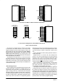
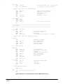
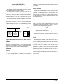
Neuron CHIP
MASTER
Neuron CHIP
SLAVE A
a. Neuron Chip–to–Neuron Chip
µP / µC
MASTER
Neuron CHIP
SLAVE A
Neuron CHIP
MASTER
µP/µC
SLAVE A
c. Neuron Chip Master/Foreign Processor
µP / µC
MASTER
Neuron CHIP
SLAVE B
µP/µC/PERIPHERAL
DEVICE
µP/µC/PERIPHERAL
DEVICE
Neuron CHIP
SLAVE A
Neuron CHIP
SLAVE B
b. Foreign Processor Master/Slave A
d. Foreign Processor Master/Slave B
Figure 2. Possible Master/Slave Connections for the Neuron Chip
In a non–Neuron Chip (foreign processor) interface, it is
assumed that the microprocessor or microcontroller involved
has the ability to execute the handshaking/token passing
algorithm dictated by the attached Neuron Chip. This usually
consists of a hardware interface and a software program that
duplicates the actions of a Neuron Chip.
A foreign processor master can interface to a Neuron Chip
configured in slave A (Figure 2b) or slave B (Figure 2d)
mode. In slave B mode, the foreign processor master reads
the HS bit on the data bus by accessing the control register.
In slave A mode, the HS line can be read using several
different approaches. See also the ‘‘Foreign–to–Neuron
Processor Interface’’ section.
Certain applications, such as a Neuron Chip–to–Neuron
Chip connection, have only one solution (master to slave A).
Although several possible interfacing scenarios are shown
in Figure 2, not all can be considered for every application.
ALTERNATIVES TO THE
PARALLEL I/O INTERFACE
Echelon sells a licensed firmware, Microprocessor
Interface Program (MIP), which supplies an alternative to
parallel I/O interface. As in parallel I/O, MIP also requires a
software intensive driver for the host processor. MIP was
designed to accommodate systems with complex
calculations or I/O, applications needing more than 62
network variables, and large network management
applications. The MIP resides on the Neuron Chip and no
other application can be implemented. The MIP is faster than
the parallel I/O object discussed in this application note, as
no scheduler is used and fewer buffers are needed for data
transfers. An Echelon sales representative can provide the
AN1208
AL–10
license cost, cost per node, and additional information about
the MIP.
A common way two microprocessors exchange
information is utilizing a dual–port RAM. This concept can
also be employed to allow data transfers between the
MC143150 Neuron Chip and a foreign processor. Details will
not be discussed in this application note.
The Neuron Chip also provides an asynchronous serial
data format, as in Motorola’s SCI, EIA–232 communication,
called serial input/output, and a synchronous serial data
format called NeuroWire input/output, which interfaces to
Motorola’s SPI. The serial interfaces are slower than the
parallel interface but some applications may require a serial
option.
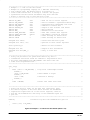
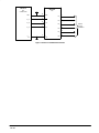
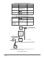
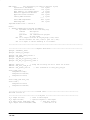
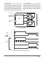
Neuron CHIP PARALLEL I/O INTERFACE
The Neuron Chip parallel I/O interface consists of eight I/O
and three control lines (see Figure 3).
The CS line is always driven by the master and, when
active, signifies that a byte transfer operation is currently in
progress. A low pulse on this line strobes the data into either
the master or slave. (Refer to Figures 8, 9, and 10.)
The type of data transfer actually taking place, either a
read or a write (with respect to the master), is assessed by
the level of the R/W line at the time the CS line is pulsed low.
The R/W line is driven by the master.
The HS (handshake) output is always driven by the slave.
It informs the master if the slave is busy. In effect the HS
output can be treated as a slave–busy signal. When high,
the slave is busy performing an action (read or write of a
command or data); a low indicates it is ready for the next
transaction. In slave A mode, HS is a physical pin and in
slave B mode, HS is the least significant bit of the control
register.
MOTOROLA LONWORKS TECHNOLOGY
MASTER
SLAVE A
IO0
IO1
IO2
IO3
D0
D0
D1
D1
D2
D2
D3
D3
D4
IO4
IO5
IO6
IO7
D0–D7
IO0
IO1
IO2
IO3
D4
D0–D7
D5
D5
D6
D6
D7
D7
IO4
IO5
IO6
IO7
IO8
CS
CS
IO8
IO9
R/W
HS
R/W
HS
IO10
IO10
IO9
a. Connections for Master and Slave A Modes of Parallel I/O
READ ONLY
CONTROL REGISTER
READ/WRITE
DATA REGISTER
HS
X
X
X
X
X
X
X
D0
D1
D2
D3
D4
D5
D6
D7
R/W = 1
IO10 = 1
R/W = 0
or
IO10 = 1
SLAVE B
D0/HS
D1
D2
D3
HS/D0–D7
D4
D5
D6
D7
R/W = 0 or 1
IO10 = 0
IO0
IO1
IO2
IO3
IO4
IO5
IO6
IO7
CS
IO8
R/W
A0
IO9
IO10
b. Connections and Registers for Slave B Mode of Parallel I/O
Figure 3. Parallel Interface
The I/O10 pin is a register select pin, driven by the master
for interface to the slave B mode. It can be the least
significant address bit which selects between reads of the
data register and the control register. An even address
typically allows data transfers and reads of an odd
address allow HS monitoring. The remaining bits of the
control register are unused and indeterminate and therefore
should be masked by the software.
It is possible for the master device to come online and poll
the HS line before the slave has had a chance to set the
proper level on this line. To prevent the master from reading
invalid data on the HS line, a pull–up resistor should be used
on the HS line of a slave A Neuron Chip or the HS/D0 line of
a slave B Neuron Chip.
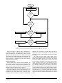
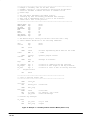
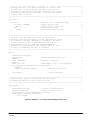
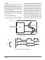
Token–Passing Protocol
A token–passing protocol implemented by the Neuron Chip
firmware permits the coexistence of multiple devices on a
common bus. At any given time, only one device is given the
option of writing to the bus. A virtual write token is passed
alternately between the master and the slave on the bus in
an infinite, ping–pong fashion. The owner of the token has
the option of writing data, or alternatively, passing the token
without any data. The token is not physically passed
MOTOROLA LONWORKS TECHNOLOGY
between the processors but is tracked with software. A token
is acquired after a read cycle and relinquished after a write
cycle. See also the ‘‘Neuron C Resources’’ section of this
text.
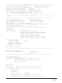
Figure 4 illustrates the token passing operation between a
master and a slave.
Multiple slaves on a common bus, with multiple write
tokens, can also be supported by the token – passing
protocol. In such a case, the master must keep track of all
outstanding write tokens and accordingly direct bus traffic.
Slaves may be selected round robin or on a priority basis.
Uniquely assigned CS lines prevent bus contention.
Once in possession of the write token, a device may
perform one of several operations (as shown in Figure 4):
write data, pass token, resynchronize (master only), or
acknowledge resynchronization (slave only).
The sequence of events for each of the above operations
is always the same, for either the master or the slave (A or
B). However, the degree to which the user is exposed to the
underlying token–passing operations is varied depending on
the actual device involved. Built–in tools within the Neuron C
language allow for straightforward software coding of the
Neuron Chip. This translates to a transparent token–passing
protocol, which in turn results in program simplicity.
AN1208
AL–11
RESET
MASTER RESYNC
SLAVE
ACKSYNC
?
NO
YES
YES
MASTER HAS
TOKEN:
RESYNC?
NO
MASTER DATA WRITE
SLAVE DATA WRITE
YES
MASTER HAS
TOKEN: DATA
TO XFER?
NO
YES
SLAVE HAS
TOKEN: DATA
TO XFER?
NO
MASTER NULL WRITE
SLAVE NULL WRITE
Figure 4. Token–Passing Protocol Sequence Between Master and Slave
On the other hand, if a Neuron Chip is interfaced to a
non–Neuron processor (foreign processor), the user must
explicitly implement the handshaking/ token – passing
protocol on the foreign processor side. Although the Neuron
Chip software remains straightforward, the data transfer rate
may be affected by the additional cycle needed for the
foreign processor to read the HS and the code needed to
implement the token tracking.
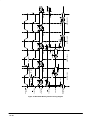
Protocol Commands
The byte format of the command options available to the
token holder are shown in Figure 5. Each command is made
up of a fixed sequence of read and write operations to the
bus by both the master and the slave. The state transition
diagram for each command is shown in Figure 6.
These commands are the building blocks on which all
communication between a Neuron Chip parallel I/O and the
outside world are based. Only one of the commands can be
performed by the token holder at any given time. Upon
completion of the command, the token is automatically
AN1208
AL–12
owned by the other device. The other device now has the
opportunity to execute a command. The write token is thus
passed back and forth between the master and slave
indefinitely.
The owner of the token (either master or slave, Neuron
Chip or foreign processor) can hold the token for an indefinite
period of time. (Refer to Figure 4.) However, after passing
the token to a Neuron Chip (master or slave) a check must
be implemented periodically to verify if the Neuron Chip is
ready to write to the bus. If the Neuron Chip is a
token–holding slave, the master should monitor the HS line
for a low state indicating the slave is ready to output to the
bus. If the Neuron Chip is a token–holding master, the slave
should toggle HS low to see if the master is ready to output to
the bus. A Neuron Chip watchdog time–out may occur if
communication is not completed within approximately 840
milliseconds (10 MHz) after the Neuron Chip I/O output is
ready. The watch dog scales proportionally to the external
clock.
MOTOROLA LONWORKS TECHNOLOGY
WRITE DATA COMMAND
CMD_XFER
LENGTH
PASS TOKEN COMMAND
(NULL WRITE)
CMD_NULL
EOM
RESYNC COMMAND
(MASTER ONLY)
CMD_RESYNC
EOM
ACKSYNC COMMAND
(SLAVE ONLY)
CMD_ACKSYNC
EOM
NOTES:
CMD_XFER = 0x01
CMD_NULL = 0x00
CMD_RESYNC = 0x5A
CMD_ACKSYNC = 0x07
DATA BYTE
DATA BYTE
EOM
EOM = Any Byte (usually 0x00)
Length = # of Data Bytes (not including EOM)
Data = Actual Data Bytes
Figure 5. Commands Available to the Token Holder
If the Neuron Chip slave receives any command byte other
than CMD_XFER, CMD_NULL, or CMD_RESYNC it will go
into a wait clause until a CMD_RESYNC is received or a
watch dog time out occurs.
Read and write operations require a negative pulse (high
to low to high) on the CS line (Figures 8, 9, and 10). For the
slave B write operation, a high to low CS transition causes
the slave B to put the data on the bus so that it can be latched
(strobed) in by a master. For a Neuron Chip slave A write, the
Neuron Chip continues to drive the data until a low pulse is
detected on CS, indicating the master has latched the data.
In the case of the master write operation, both the Neuron
Chip slave A and slave B read (strobe) the data on the rising
edge of CS.
The low to high transition of the CS causes the Neuron
Chip slave (A or B) HS signal to go high. The only exception
to this is when the master reads the control register of a slave
B. HS is unaffected in this case.
As shown in Figure 6, the EOM byte always terminates a
command and is never read by the device it is sent to. The
EOM transaction is just a write cycle and is used by the slave
to toggle the state of HS at the end of a command in order to
pass the write token.
Handshake
The handshake (HS) signal acts like a slave busy flag
to ensure valid data transfers (Figures 8, 9, 10). Slave A
has an external HS line and slave B write HS as a control bit
in the control register. See Figure 3. The Neuron Chip HS
line is hardware controlled, not firmware controlled.
When the master executes a data transfer, the Neuron
Chip slave toggles the HS signal high. When the slave has
completed reading a byte or is ready to write, HS is low.
Therefore, HS = 1 indicates the slave is busy and valid
data transfers can not be initiated by the master until HS
= 0.
When a foreign processor is the master, HS must be
explicitly polled by that processor’s software routine to
ensure HS is low before a read or write operation is initiated
(controlled by the CS and R/W lines).
MOTOROLA LONWORKS TECHNOLOGY
Synchronization
Upon a Neuron Chip reset, the write token is, by definition,
in the possession of the master. Synchronization across the
parallel bus is required by the Neuron Chip following any
reset condition. The purpose of synchronization is to ensure
both the master and slave are ready for data transaction.
Synchronization prevents false starts of data transfers or
incorrect data transfers. This is automatically accomplished
by the Neuron Chip through the use of a synchronization
sequence.
The Neuron Chip’s automatic synchronization process
occurs just before the reset clause of the application program
is executed, and just after configuration of the Neuron Chip’s
I/O pins. Prior to the synchronization sequence, the I/O pins
are configured as inputs.
The automatic synchronization sequence carried out by
the Neuron Chip is dependent on the mode of its parallel I/O
object. If the Neuron Chip is a master, it will initiate a
resynchronization command upon reset. If the Neuron Chip
is a slave (A or B), it will await the arrival of a
resynchronization command from the master (any other
command will be ignored).
The parallel I/O object provides the capability to
synchronize the devices at any time when a foreign
processor is the master. This enables the foreign processor
to ascertain the integrity of the communication medium and
reestablish a predetermined state. Aside from the initial
synchronization necessary after a reset, a foreign processor
is not required to perform this operation at any other time.
The capability, however, is provided for the system designer
in case a need does arise.
The resynchronization operation can be initiated by the
token–holding master at any time by the use of the RESYNC
command. The RESYNC command sends a special
message (CMD_RESYNC) to the slave, which in turn
triggers it to send its own special message
(CMD_ACKSYNC) back to the master. Thus, a two–way
communication has taken place and the token has been
passed from the master to the slave and back to the master
again.
AN1208
AL–13
COMMAND:
WRITE DATA
MASTER HAS
WRITE TOKEN
(R/W = 0)
HS = 0
MASTER WRITES
CMD_XFER
HS = 1
SLAVE READS
CMD_XFER
HS = 0
MASTER WRITES
LENGTH BYTE
HS = 1
SLAVE READS
LENGTH BYTE
HS = 0
MASTER WRITES
A DATA BYTE
HS = 1
SLAVE READS
DATA BYTE
HS = 0
MASTER WRITES
NEXT DATA BYTE
HS = 1
SLAVE READS
DATA BYTE
HS = 0
MASTER WRITES
EOM
HS = 1
SLAVE OWNS
WRITE TOKEN
PASS TOKEN (NULL WRITE)
SLAVE HAS
WRITE TOKEN
(R/W = 1)
HS = 1
MASTER HAS
WRITE TOKEN
(R/W = 0)
HS = 0
SLAVE WRITES
CMD_XFER
MASTER WRITES
CMD_NULL
HS = 1
HS = 0
MASTER READS
CMD_XFER
HS = 1
SLAVE READS
CMD_NULL
HS = 0
SLAVE WRITES
LENGTH BYTE
HS = 0
MASTER WRITES
EOM
HS = 1
MASTER READS
LENGTH BYTE
SLAVE OWNS
WRITE TOKEN
HS = 1
SLAVE HAS
WRITE TOKEN
(R/W = 1)
HS = 1
SLAVE WRITES
CMD_NULL
HS = 0
MASTER READS
CMD_NULL
HS = 1
SLAVE WRITES
EOM
HS = 0
MASTER OWNS
WRITE TOKEN
RESYNC
ACKSYNC
MASTER HAS
WRITE TOKEN
(R/W = 0)
SLAVE HAS
WRITE TOKEN
(R/W = 1)
HS = 0
MASTER WRITES
CMD_RESYNC
HS = 1
SLAVE READS
CMD_RESYNC
HS = 0
MASTER WRITES
EOM
HS = 1
SLAVE OWNS
WRITE TOKEN
HS = 1
SLAVE WRITES
CMD_ACKSYNC
HS = 0
MASTER READS
CMD_ACKSYNC
HS = 1
SLAVE WRITES
EOM
HS = 0
MASTER OWNS
WRITE TOKEN
MASTER REPEATS
RESYNC UNTIL SLAVE
GENERATES ACKSYNC
SLAVE WRITES
A DATA BYTE
HS = 0
MASTER READS
DATA BYTE
HS = 1
SLAVE WRITES
NEXT DATA BYTE
HS = 0
MASTER READS
DATA BYTE
HS = 1
SLAVE WRITES
EOM
HS = 0
•
•
•
•
CS and R/W are controlled by the master.
HS is controlled by the slave. HS = 1: slave is busy, HS = 0: slave is ready.
Master read and write operations are performed by a negative pulse on the CS line.
In the slave B mode, the master polls the status of the HS line by reading the control
register of the slave (A0 = 1). The only difference between this type of read and a data
register read is that the state of the HS is unaffected.
• The EOM is never read.
MASTER OWNS
WRITE TOKEN
Figure 6. Micro–Operations of the Handshake Protocol
The operations described by Figure 6, including the
synchronization operations, are transparent to the Neuron
Chip application programmer. They are automatically
executed by the Neuron Chip’s firmware. When interfacing a
foreign processor to the Neuron Chip, however, the
above–mentioned operations must be explicitly carried out by
the attached processor.
Reset
Depending on the user application, the reset lines may
need to be monitored to ensure the integrity of the
transmission. The foreign processor master reset can
directly control the Neuron Chip slave reset. However, the
master might handle a slave reset with an interrupt service
routine. A reset circuit is shown in Figure 7.
AN1208
AL–14
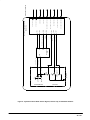
MC68HC11 to Neuron Chip Interface Reset Circuitry
Reset signals from and to the Neuron Chip are handled by
additional logic as shown in Figure 7. There are two sources
of reset for the MC68HC11 and the Neuron Chip. One source
internally generated by the MC68HC11 or Neuron Chip and
the second source externally generated by a Low Voltage
Inhibit (LVI), for example, an MC33164 or a push–button
reset switch.
The MC68HC11 may reset the Neuron Chip but not
vice–versa.
Additionally, resets may come from the Neuron Chip by a
network management command being received over the
LONWORKS network. This network management command
causes the reset pin on the Neuron Chip to become an
output and be pulsed low for a short period of time. Due to
the short duration of this pulse, this reset condition must be
MOTOROLA LONWORKS TECHNOLOGY
68HC11
IRQ
PD4
MC74HC74A
VDD
Neuron CHIP
R
D
PD2
VDD
Q
C
Q
S
OPEN
COLLECTOR
RESET
RESET
VDD
100 pF
MC33164
IN
OUT
GND
RESET
100 pF
VDD
LED
SERVICE
RESET
SLAVE B MODE
Figure 7. Reset Scheme for the Neuron Chip Interfacing to a MC68HC11 Processor
latched (for instance, a 74HC74 D flip–flop). The output of
the D flip–flop is then used to interrupt the MC68HC11 to
notify the application program of this network management
command. Since this signal is an interrupt to the MC68HC11,
the IRQ pin must be held low until the interrupt is
acknowledged by the interrupt service routine. The interrupt
is then cleared by setting PD2 I/O pin low and restoring it
back high in the interrupt service routine. Optionally, in case
of multiple IRQ interrupts, the output of the flip–flop may also
be used as an input to another I/O pin (such as PD4) so that
the interrupt service routine may determine the source of the
IRQ interrupt.
The open collector device between the MC68HC11 reset
pin and the Neuron Chip reset pin is used to prevent a
Neuron Chip source reset from resetting the MC68HC11.
When designing the reset circuit several factors must be
taken into consideration, these include:
• How much current the Neuron Chip can source.
• The saturation voltage of the LVI. This voltage will be
current dependent.
• The voltage level the Neuron Chip will reset.
• The voltage level the Neuron Chip will output a reset.
• The current level any LEDs will turn on.
• Voltage drops across all components including diodes
and resistors.
• Any time constants (ex: RC networks).
• Saturation voltage of the open collector device.
MOTOROLA LONWORKS TECHNOLOGY
Other reset circuits could be designed to fit specific
applications. See also the appropriate technical data sheets
for the suggested power_on_reset circuits and other reset
issues.
Neuron C RESOURCES
The Neuron C programming language allows access to
the parallel I/O object. The following section describes the
available resources within the Neuron C programming
language.
The parallel I/O object is declared in a Neuron C program
using the following syntax (more details are given in
Figure 12 of this document and the LonBuilder Neuron C
Programmer’s Guide [Motorola document order number
NEURONCPG/AD].)
IO_0 parallel slave/slave_b/master io_object_name;
The functions io_in and io_out are used as parallel
reads and writes, respectively. To use the parallel I/O object
of the Neuron Chip, i o _ i n and i o _ o u t require a
parallel_io_interface structure as defined below:
Struct parallel_io_interface {
unsigned length;
//length of data field
unsigned data[maxlength]; //data field
}pio_name;
The previous structure must be declared, with an
appropriate definition of maxlength signifying the largest
expected buffer size for any data transfer.
AN1208
AL–15
In the case of io_out, length is the number of bytes to
be transferred out and is set by the user program. In the case
of io_in, length is the maximum number of bytes to be
transferred in. If the incoming length is larger than length
then the incoming data stream is truncated to length bytes.
The length field must be set before calling either io_in
or i o _ o u t. The maximum value for the l e n g t h and
maxlength field is 255.
The parallel I/O object of the Neuron Chip is easily
accessed with the use of built–in Neuron C functions and
events. The following functions and events are provided
specifically for use with the parallel I/O object:
• io_in_ready
This event becomes TRUE whenever a
message arrives on the parallel bus
that must be read. The application must
then call io_in to retrieve the data.
• io_out_request This function is used to request an
indication for an I/O object. It is up to the
application to buffer the data until the
io_out_ready event is TRUE.
• io_out_ready This event becomes TRUE whenever
the parallel bus is in a state where it can
be written to and the io_out_
request function was previously
invoked. The application must then call
the io_out function to write the data to
the parallel port.
Neuron C applications may be written that use the parallel
bus in a unidirectional manner (i.e., applications may be
written without either an io_in_ready or io_out_ready
when clause). In the case where no io_in function exists, it
is up to the programmer to assure that no read transfers of
real data messages will ever be required by the application.
This is to protect the device on the other side of the bus from
waiting forever on a data transfer.
If there is no data to be transferred, the programmer simply
does not generate an in_out_request. No additional code
is needed for passing the token (CMD_NULL). The
CMD_NULL generation is part of the transparent token
passings protocol of the Neuron Chip.
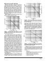
TIMING
Figures 8, 9, and 10 give the detailed timing specifications
for the parallel I/O object. All three modes of the object are
included. Note that these are typical observed numbers and
are not meant to replace actual device characterization.
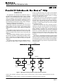
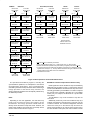
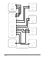
RAM ALLOCATION
If transferring large packets of data from the
communication port (network) through the I/O port, memory
issues may be of concern. This section describes how to
determine if the on–chip RAM is adequate for a specific
application.
There are four types of buffers needed to move data
between the application program and the communication
port (network). They are: the network input buffers, the
application input buffers, the application output buffers and
the network output buffers. As shown in Figure 11, the
network buffers allow communication between the media
AN1208
AL–16
access control (MAC) processor and the network processor,
and the application buffers allow the network processor and
application processor to communicate.
The Neuron Chip accepts messages from the network into
the network input buffers, verifies the CRC, and interprets
the destination address. Therefore, the size of the network
input buffers must support the largest potential message
transmitted over the channel in order to prevent error
conditions. The LonBuilder Developer’s Workbench default
size for each of these buffers is 66 bytes and the default
count is two buffers on the MC143150. The default memory
allocation for these buffers is on–chip RAMFAR.
In a condition when the count of Neuron Chip input buffers
is not sufficient to support traffic on a network, the Neuron
Chip does not overwrite data in the buffers, but instead
ignores the incoming packet. If, for example, the network
message is specified as an ‘‘acknowledged service with
retries’’ the message is not lost immediately. The source
Neuron Chip instead continues to resend the message until
either an acknowledgement is received or the maximum
retries are sent.
Likewise, the Neuron Chip does not overwrite data in
the output buffers. Refer to the documentation on the
‘‘Preemption Mode’’ in the Neuron C Programmer’s Guide for
details on specifying preemption. If the network is active, an
increase in the count of buffers may be needed. In any case,
data is never overwritten.
Application variables, including the parallel I/O application
structure(s), are also stored in RAM. By default, user RAM is
stored in the 256 bytes available in RAMNEAR; however,
RAMFAR can also be employed for user RAM.
The MC143150 has 2K of on–chip RAM. The LonBuilder
Developer’s Workbench allocates memory for both the
system data (i.e., stack) and for the transaction control block.
The remaining memory available for the input and output
buffers is potentially less than 1K, depending on memory
needed for user RAM. The MC143120 has 1K of RAM and
may not be suitable for channels with large packet transfers.
For example, if the value of 114 bytes is selected for all the
four types of I/O buffers and the counts selected are two,
then the total number of I/O buffers is eight. In this case, no
external RAM should be needed if the user RAM does not
exceed the 256 bytes of RAMNEAR. Note: 114 bytes × 8
(4 buffers × count 2) = 912 bytes needed for all I/O buffers.
The overhead for the application buffers is maximum 7 bytes
and the overhead for the network buffers is 25, therefore,
maximum data length in this scenario is 89 (114 – 25) bytes.
Refer to the memory management section of the Neuron C
Programmer’s Guide for allowed buffer values.
In some applications, large packets of data are transfered
in only one direction. If the value assigned to the output
buffers is 210 bytes, then the average of the input buffers
could potentially be given the value of up to 42 bytes without
external memory (210 bytes × 4 output buffers + 42 bytes × 4
input buffers = 1008 bytes total RAM needed). Again, the
count is left to its default of 2. The maximum potential actual
data output size is 185 bytes (210 – 25 overhead = 185).
Note, the size of the network input buffers is determined by
the largest potential packet transmitted on the channel. The
application input buffers need only accomodate the largest
packet destined for a particular Neuron Chip.
MOTOROLA LONWORKS TECHNOLOGY
CS
tmhscs
tmcspw
tmcspw
tmhsv
tmhsv
tmhsh
tmhsh
HS
tmrws
tmrwh
tmrws
tmhsdv
R/W
tmrdz
tmwdh
tmwds
tmwdd
DATA OUT
tmrds
tmrdh
DATA IN
READ CYCLE
Parameter
WRITE CYCLE
Description
Min
Typ
Max
tmrws
R/W setup before falling edge of CS
150 ns
3 CLK1
—
tmrwh
R/W hold after rising edge of CS
100 ns
—
—
CS pulse width
150 ns
2 CLK1
—
0 ns
—
—
150 ns
10 CLK1
—
—
—
25 ns
0 ns
—
—
2 CLK1
6 CLK1
—
0 ns
—
—
150 ns
2 CLK1
—
—
50 ns
—
tmcspw
tmhsh
HS hold after falling edge of CS
tmhsv
HS checked by firmware after rising edge of CS
tmrdz
Master three–state DATA after rising edge of R/W
tmrds
Read data setup before falling edge of HS 3
tmhscs
HS low to falling edge of CS 5
tmrdh
Read data hold after falling edge of CS
tmwdd
Master drive of DATA after falling edge of R/W
tmhsdv
HS low to data valid 5
tmwds
Write data setup before rising edge of CS
150 ns
2 CLK1
—
tmwdh
Write data hold after rising edge of CS 1
Note 1
—
—
NOTES:
1. Master will hold output data valid during a write until the Slave device pulls HS low.
2. CLK1 represents the period of the Neuron Chip input clock (100 ns at 10 MHz).
3. HS high is used as a slave busy flag. If HS is held low, the maximum data transfer rate is 24 CLK1s (2.4 µs @
10 MHz) per byte. If HS is not used for a flag, caution should be taken to ensure the master does not initiate a data
transfer before the slave is ready.
4. In a master read, CS pulsing low acts like a handshake to flag the slave that data has been latched in.
5. Parameters were added in order to aid interface design with the Neuron Chip.
Figure 8. Master Mode Timing
MOTOROLA LONWORKS TECHNOLOGY
AN1208
AL–17
CS
tsahsv
tsahsv
tsacspw
tsacspw
tsahsh
tsahsh
HS
tsarws
tsarwh
tsarws
R/W
tsawdd
tsardh
tsards
DATA IN
tsawds
tsawdh
tsardz
DATA OUT
WRITE CYCLE
(MASTER READ)
Parameter
READ CYCLE
(MASTER WRITE)
Description
Min
Typ
Max
tsarws
R/W setup before falling edge of CS
25 ns
—
—
tsarwh
R/W hold after rising edge of CS
0 ns
—
—
CS pulse width
45 ns
—
—
tsahsh
HS hold after rising edge of CS
0 ns
—
—
tsahsv
HS valid after rising edge of CS
—
—
50 ns
tsawdd
Slave A drive of DATA after rising edge of R/W
25 ns
—
—
tsawds
Write data valid before falling edge of HS
150 ns
2 CLK1
—
tsawdh
Write data valid after rising edge of CS
150 ns3
2 CLK1
—
tsardz
Slave A three–state DATA after falling edge of R/W
—
—
25 ns
tsards
Read data setup before rising edge of CS
25 ns
—
—
tsardh
Read data hold after rising edge of CS
5 ns
—
—
tsacspw
NOTES:
1. CLK1 represents the period of the Neuron Chip input clock (100 ns at 10 MHz).
2. In slave A mode the HS signal is high, a minimum of 4 CLK1 periods. The typical time HS is high during consecutive
data reads or consecutive data writes is also 4 CLK1 periods.
3. If tsarwh < 150 ns, then tsawdh = tsarwh.
Figure 9. Slave A Mode Timing
AN1208
AL–18
MOTOROLA LONWORKS TECHNOLOGY
CS
tsbcspw
tsbcspw
tsbah
A0
tsbas
tsbrwh
tsbrws
R/W
tsbrdh
tsbrws
tsbrds
DATA IN
tsbwdz
tsbwdv
tsbwdh
DATA OUT
WRITE CYCLE
(MASTER READ)
Parameter
READ CYCLE
(MASTER WRITE)
Description
Min
Typ
Max
tsbrws
R/W setup before falling edge of CS
0 ns
—
—
tsbrwh
R/W hold after rising edge of CS
0 ns
—
—
CS pulse width
Note 1
—
—
tsbas
A0 setup to falling edge of CS
10 ns
—
—
tsbah
A0 hold after rising edge of CS
0 ns
—
—
—
—
50 ns
0 ns
30 ns
—
tsbcspw
tsbwdv
CS to write data valid
tsbwdh
Write data hold after rising edge of CS
tsbwdz
CS rising edge to slave B release data bus
—
—
50 ns
tsbrds
Read data setup before rising edge of CS
25 ns
—
—
tsbrdh
Read data hold after rising edge of CS
5 ns
—
—
NOTES:
1. The slave B write cycle (master read) CS pulse width is directly related to the slave B write data valid parameter and master
read set–up parameter. To calculate the write cycle CS duration needed for a specific application use:
tsbcspw = tsbwdv + master’s read data setup before rising edge of CS
Refer to the Master’s Specification Data Book for the master read set–up parameter. The slave read cycle minimum CS pulse
width = 50 ns.
2. In a slave B write cycle the timing parameters are the same for a control register (HS) write as for a data write.
3. Special Applications: Both the state of CS and R/W determine a slave B write cycle. If CS cannot be used for a data transfer
then toggling the R/W line can be used with no changes to the hardware. In other words, if CS is held low during a slave B
write cycle, a positive pulse (low to high to low) on R/W can execute a data transfer. The low to high transition on R/W causes
slave B to drive data with the same timing parameters as tsbwdv (redefined R/W to write data valid). Likewise, the falling edge
of R/W causes slave B to release the data bus with the same timing limits as the CS rising edge in tsbwdz. This scenario is
only true for a slave B write cycle and is not applicable to a slave B read cycle or any slave A data transitions. This application
may be helpful if the master has separate read and write signals but no CS signal. Caution must be taken to ensure the bus
is free before transfers to avoid bus contention.
Figure 10. Slave B Mode Timing
MOTOROLA LONWORKS TECHNOLOGY
AN1208
AL–19
COMMUNICATION PORT (CP0 – CP4)
INPUT/OUTPUT PORT (IO0 – IO10)
MAC
PROCESSOR
66
NETWORK
PROCESSOR
66
66
66
APPLICATION
PROCESSOR
66
NETWORK I/O BUFFERS
(2 INPUT, 2 OUTPUT)
RAMFAR
66
66
APPLICATION I/O
BUFFERS
(2 INPUT, 2 OUTPUT)
66
256
USER BUFFER
RAMNEAR
(TO BASE PAGE)
Figure 11. LonBuilder 2.1 Developer’s Workbench Default for RAM Allocation
(Excluding Priority Buffers)
Following the same calculations as shown above, if the
input buffers are assigned the value of 210, then the output
buffers could potentially be 42 without external memory.
If the Neuron Chip requires the size of 210 for the network
input buffers to accommodate the largest packet on the
channel, the potential size of the output buffers is related to
the size of the application input buffers.
In a scenario where the maximum value of 255 bytes is
required for output, the source Neuron Chip could potentially
need external memory. Additionally, the destination Neuron
Chip will potentially need external memory, depending on the
size of the outgoing messages. Note all the Neuron Chips on
the channel need to accommodate this packet (all network
input buffers must equal 255 on all Neuron Chips on the
channel).
Pragmas allow the Neuron C programmer to change the
size of any of the four buffers, change the count of any of the
four buffers, or change the count of the priority buffers. Some
examples follow; refer also to the memory management
section of the Neuron C Programmer’s Guide for additional
examples:
#pragma
#pragma
#pragma
#pragma
#pragma
#pragma
#pragma
net_buf_in_size
app_buf_in_size
net_buf_out_size
app_buf_out_size
net_buf_in_count
net_buf_out_priority_count
app_buf_out_priority_count
210
114
42
42
3
0
0
The LonBuilder Developer’s Workbench provides memory
allocation information for a specific application by choosing
the Output Link Summary build option in the Options / project
pull down menus. The Build All option, under the Project pull
down menu, stores the memory allocation information in a
build.log file which can be viewed through the LonBuilder
Developer’s Workbench editor.
AN1208
AL–20
Priority buffers and authentications require additional
buffer allocation and are not considered in the previous
examples. The LonBuilder Developer’s Workbench by
default assigns priority buffers; therefore, pragmas are
required to release this memory space.
Neuron CHIP–TO–Neuron CHIP INTERFACE
The parallel connection of one Neuron Chip to another is
accomplished by assigning one as the master device and the
other as a slave A device. The hardware requirements in this
case reduce to a direct, one–to–one, connection of all eleven
I/O pins on both sides.
Figure 12 illustrates a typical parallel I/O processing
interface routine which would reside on the slave (A) Neuron
Chip. Information is transferred through the I/O port and is
never transmitted over the network in this example.
FOREIGN–TO–Neuron PROCESSOR
INTERFACE (SLAVE B MODE)
Slave B mode was designed to interface the Neuron Chip
to a foreign processor master.
This section illustrates an M68HC11 (HC11) acting as a
master to a Neuron Chip configured in slave B mode. The
Neuron Chip looks like a peripheral device residing on the
HC11’s address bus. The hardware interface is shown in
Figure 13. ECLK is gated twice for CS in order to ensure
timing compatibility for the HC11’s read data hold parameter.
External address decoding logic allows the HC11 to
access the Neuron Chip by using specific addresses (one
address for the data register (A0 = 0) and one for the control
register (A0 = 1)). The decoding circuitry in Figure 13
specifically memory maps the Neuron Chip to addresses
between hex 4000 and hex 7FFF. This section of memory
was chosen because it had the simplest decoding circuitry
for this specific example’s available memory map. In
particular, this example software specifies address 4000 for
the data register and 4001 for the control register.
MOTOROLA LONWORKS TECHNOLOGY
************************************************************************
* Example 1
* This Neuron C example program configures the Neuron Chip in slave A
* mode.
************************************************************************
IO_0 parallel slave s_bus;
#define DATA_SIZE 255
//maximum data field allowed
struct parallel_io_interface
{
unsigned int length;
//length of data field
unsigned int data[DATA_SIZE];
}piofc
when (io_in_ready(s_bus))
//ready to input data
{
piofc.length = DATA_SIZE;
//maximum number of bytes
to read
io_in(s_bus,&piofc);
//get 10 bytes of
incoming data
}
when (io_out_ready(s_bus))
//ready to output data
{
piofc.length = 10;
//number of bytes to write
io_out(s_bus,&piofc);
//output 10 bytes from buffer
}
when (...)
//user defined event
indicating buffer has been filled
{
io_out_request(s_bus);
//post the write transfer
}
request
Figure 12. Example 1 — Neuron C Program for the Neuron Chip
68HC11A1
EXPANSION
BUS
Neuron CHIP
I/O DATA
LINES
A15
CS
IO_8
A14
74HC04
74HC32
*ECLK
74HC04
8
AD0 – AD7
8
A0
AD0
LE
AS
D0 – D7 OR HS
IO_0 – IO_7
IO_10
OE
74HC373
R/W
R/W
IO_9
Figure 13. Interfacing the Neuron Chip (Slave B) to the M68HC11A1
(*ECLK Must be Gated Twice for Interface Timing Requirements)
MOTOROLA LONWORKS TECHNOLOGY
AN1208
AL–21
The HC11’s least significant byte of the address bus is
multiplexed with its data bus. As A0 – A7 is valid the first half
of the HC11’s E–clock (ECLK) cycle and the data, D0 – D7, is
valid the last half of the HC11’s E–clock cycle, a 74HC373
was used to latch A0. Therefore, A0 controls access to the
data register or the control (HS) register.
The M68HC11EVM (EVM) evaluation board was used for
this example, as the address and data lines are easily
accessible through the existing expanded mode connector.
An MC68HC11A1 is supplied with the EVM board. The EVM
board provides an 8 MHz external crystal and supports 2
MHz bus operations. The specified bus cable length is
6 inches.
The M68HC11EVBU also brings the address and data
lines to the external world through an expanded mode
connector and could be used with adjustments to this
example’s software memory mapping and external decoding
circuitry. The M68HC11EVB evaluation board is not
suggested as the address and data lines appear as general
purpose I/O lines on the connectors and cannot easily
support peripheral memory mapped devices.
Another option includes Motorola’s M68HC11EVS.
The LonBuilder Developer ’s Workbench I/O cards
(Echelon part number 27800 or 27810; contact an Echelon
salesperson) may be used to access the I/O pins from the
Neuron emulator unit. The LonBuilder Developer ’s
Workbench Startup and Hardware Guide describes how to
configure the jumpers for parallel I/O and suggests I/O_9
(R/W) be tied to the master’s I/O buffers circuitry to configure
(on the fly) the I/O lines for either input or output mode. As
per this example, the slave will need the R/W line inverted
before connecting to the I/O buffers or alternately the pull up
on the I/O buffer schematic can be configured as a pull down.
The eight bidirectional I/O data lines are configured on
jumpers JP15 – JP8. Motorola also provides a direct connect
transceiver board (M143204EVK).
The Neuron C code listing (Figure 14) which interfaces the
Neuron Chip with an HC11 can also be used for Neuron
Chip–to–Neuron Chip interface by declaring the I/O object a
slave instead of a slave_b. Due to the transparent nature of
the communication protocol at the Neuron C programming
level, the Neuron Chip programmer need not be aware that
the interface is to an M68HC11 (or any other foreign
processor for that matter) instead of to another Neuron Chip.
For the M68HC11, an assembly program listing (Figure 15)
and also a C program listing (Figure 16) is provided in this
application note. Either program may be chosen for the
HC11. An IASM11 assembler is provided with the EVM.
Additional software tools, including C compilers for the HC11,
are available (contact a Motorola salesperson). It is not
recommended to use the bulletin board C compilers
designed for the HC11.
The HC11 watchdog time–out option was not implemented
in this code but can be included for further reliability
purposes.
In the code presented in Figures 14 – 16, both the Neuron
Chip and the HC11 always have data to send. Therefore, the
NULL command which simply passes the token without data
transfer is not implemented.
As seen in Table 1, the processing time required by the
Neuron Chip for the HC11 CMD_XFER and length bytes,
which preceeds the actual data transfer, greatly affects the
overall performance of the Neuron Chip.
However, all the HC11 byte reads, per the assembly code
provided in Figure 15, are dependent on the HC11 speed.
Therefore, the overall performance is dependent both on
the processing time of the Neuron Chip and the speed of
the HC11.
Typical timing using the master HC11 assembly code
(from Figure 15) and the slave B Neuron C code (from
Figure 14) is given in Table 1.
Table 2 shows the overall performance of the Neuron Chip
slave B interfacing to a foreign processor master. The HC11
code from Figure 15 was utilized. The size of the data buffer
varied with the data length.
The Neuron C code, from Figure 14, was also used to
acquire the data in Table 2. The buffer size assigned in the
Neuron C parallel I/O structure, as specificed by Max_ (see
Figure 14), does not affect the performance of the Neuron
Chip unless the buffer size designated is smaller than the
actual length of data being transferred. Therefore, buffer size
was adjusted accordingly.
A write/read cycle is defined as starting at the CMD_XFER
master write and ending at the following CMD_XFER master
write. Therefore, the timing in Table 2 not only considers the
actual byte transfer as discussed in Table 1, but also includes
time required by the scheduler and processing of the Neuron
C event (when) statements.
Table 1. Typical Byte Transfer Timing for
Neuron Chip Slave B–to–HC11 Master Parallel I/O Interface
HC11 Cycle
Byte
Data
Typical Process
Time (µs)
(per byte)
Typical
Time to HS Low (µs)
(per byte)
Write
CMD_XFER TO LENGTH
01
730
719
Write
LENGTH TO FIRST DATA
05
207
197
Write
FIRST DATA TO NEXT BYTE
51
37
27.5
Write
ADTL DATA
52–55
24
*
Read
CMD_XFER TO LENGTH
01
18
*
Read
LENGTH TO FIRST BYTE
06
21
*
Read
DATA
0–5
24
*
*HS was low the first loop it was tested, therefore, a faster foreign processor would improve the typical byte transfer time.
Typically, HS is low within 3.0 µs during these data transfers.
AN1208
AL–22
MOTOROLA LONWORKS TECHNOLOGY
Table 2 does not reflect network activity; increase in
network activity may increase processing time.
An HC11 NULL write occurs when the HC11 passes the
token without a data transfer. Altering the HC11 assembly
program in Figure 15, a NULL write was performed to pass
the token to the Neuron Chip and the Neuron Chip transfered
4 bytes of data to the HC11. The time for this write/read cycle
was 2.2 ms.
If the application is such that the HC11 would never
transfer data to the slave, the i o _ i n _ r e a d y event
statement can be removed and the total master read cycle
time reduces to 1.5 ms.
Resynchronizing on the fly can be implemented as a
safeguard to verify data integrity. The master initiates the
resynchronization (CMD_RESYNC) and the Neuron Chip
replies with an acknowledgement (CMD_ACKSYNC). The
resynchronization does not affect data waiting to be
transferred.
Utilizing a program similar to the HC11 assembly program
shown in Figure 15, the typical time for resynchronization is
less than 940 µs. The Neuron C program, from Figure 14,
was employed with no modifications (as Neuron Chip
synchronization is not handled by the application).
Table 2. Typical Write/Read Cycle Timing
Interfacing the Neuron Chip in Parallel I/O
Slave B Mode to the HC11 Master
HC11 Write
(# of Data Bytes)
HC11 Read
(# of Data Bytes)
Typical Time for
One Write/Read
Cycle (ms)
1
4
2.4
5
4
2.5
20
4
2.9
60
4
3.8
200
4
7.2
************************************************************************
** Example 2. Neuron C code slave B mode
** Program for a Neuron Chip in parallel I/O interface with
** an M68HC11. The Neuron Chip is in slave B mode and the HC11 is acting
** as a master. The program enters in an infinite loop of read and
** write cycles.
************************************************************************
#define MAX_ 10
//buffer size is ten
IO_0 parallel slave_b p_bus;
unsigned char i=0;
unsigned char maxin=10, len_out=4;
struct parallel_io
{
unsigned char len;
unsigned char buf[MAX_];
}pio;
when (io_in_ready(p_bus))
{
pio.len = maxin;
io_in(p_bus,&pio);
io_out_request(p_bus);
}
when (io_out_ready(p_bus))
{
pio.len=len_out;
for (i=0; i<len_out; i++)
pio.buf[i] = i;
io_out(p_bus,&pio);
}
//counter to fill buffer
//# of bytes for input and output
//actual number of bytes in buffer
//array to store data
//name of structure
//maximum input length
//read in data
//number of bytes to be output
//fill buffer with data
//output data
Figure 14. Example 2 — Neuron C Code Slave B Mode
MOTOROLA LONWORKS TECHNOLOGY
AN1208
AL–23
********************************************************************
** Example 3. Assembly code for the HC11 master
** Assembly listing of a test program for master/slave B mode where
** master is resident on 68HC11 and slave is resident on the
** Neuron Chip.
**
** The code below implements the 68HC11 portion,
** receiving any data and sending pre–defined data messages.
** This code is implemented more as a test of the interface
** rather than a test of the protocol.
*********************************************************************
NEURON_ADDR
DEBUG_ADDR
HS_MASK
MAXMSGLEN
EOM
TRUE
FALSE
CMD_RESYNC
CMD_ACKSYNC
equ
equ
equ
equ
equ
equ
equ
equ
equ
$4000
$0030
$01
$20
$0
$1
$0
$5A
$07
** The Neuron Chip is sitting on the HC11’s data bus with a chip
** select address decode set to the following addresses:
data
control
equ
equ
$4000
$4001
ORG
$0000
XDEF
token
token
RMB 1
*boolean representing which side has the token
* token
XDEF
counter
counter
RMB l
*general purpose counter
XDEF
msgi
RMB 34
*message in structure
msgi
mi_command
mi_length
mi_data
equ
equ
equ
*location of command in the msg structure
*location of data length in the msg structure
*location of start of data in the msg structure
**
0
1
2
Program Section
ORG
$E000
***********************************************************
** start of parallel master code
***********************************************************
XDEF
start_pio
JSR
start_pio
XDEF
main_loop
LDAB
BEQ
JSR
main_loop
master_init
token
no_token
pio_write
*initialize
*load token
*if token==O, can’t write
*send code message
** Receives any messages
no_token
JSR
BRA
pio_read
main_loop
*try to read
*repeat
Figure 15. Example 3 — Assembly Code for the HC11 Master (Sheet 1 of 3)
AN1208
AL–24
MOTOROLA LONWORKS TECHNOLOGY
********************************************************************
** wait_hs
** When the Neuron CPU reads or writes to the data port, it
** initially drives the HS line high. The master must wait for HS
** to go low again before the next read from or write to the port.
********************************************************************
XDEF
wait_hs
LDAB
ANDB
BNE
RTS
wait_hs
control
#HS_MASK
wait_hs
*****************************************************************
** master_init
** Standard synchronization with the Neuron Chip.
** Continue to write the CMD_RESYNC value plus EOM until the
** slave returns the CMD_ACKSYNC value. Return owning token.
*****************************************************************
XDEF
master_init
JSR
LDAB
STAB
JSR
JSR
LDAB
CMPB
BEQ
BRA
master_init
wait_hs
#CMD_RESYNC
data
write_eom
*wait for H.S.
*
*send the resync value
*and the EOM.
wait_hs
data
#CMD_ACKSYNC
read_complete
master_init
*wait for the CMD_ACKSYNC.
*read data from the port
*repeat is not sync’ed
*****************************************************************
** pio_read
*****************************************************************
XDEF
pio_read
LDAB
ANDB
BEQ
RTS
pio_read
control
#HS_MASK
da
*load control
*no data available
** We have data available, handshake line is low
da
LDY
LDAB
STAB
INY
BNE
#msgi
data
0,Y
*set up Y index
*read data from the port
*store in message.command
have_data
*go get data, if command!=NULL
** This was token passing message (NULL)
CLR
BRA
0,Y
read_complete
*msgi.length=0
** Since the command was non–zero, get the length byte next.
have_data
JSR
LDAB
STAB
INY
STAB
wait_hs
data
0,Y
*wait for indication of data
*read data from port
*msgi.length=ACCB
counter
*set up the counter
Figure 15. Example 3 — Assembly Code for the HC11 Master (Sheet 2 of 3)
MOTOROLA LONWORKS TECHNOLOGY
AN1208
AL–25
loop_data
LDAB
BEQ
counter
read_complete
*load the counter, Z=1, if counter==0
*if counter==0, read is complete
** There is more data to be read from port.
JSR
LDAB
STAB
INY
DEC
BRA
wait_hs
data
0,Y
*wait for data available
*read byte from data port
*store byte at Y[0]
*increment Y
*decrement counter
counter
loop_data
read_complete
LDAB
#TRUE
STAB
token
JSR
wait_hs
RTS
*wait for EOM to be sent
********************************************************************
** pio_write
********************************************************************
XDEF
pio_write
LDY
LDAB
STAB
BEQ
pio_write
#msgo
0,Y
data
write_eom
*load pointer to message
*store Y[0] in ACCB
*X[0]=Y[0]
*if command!=0, then there is a message
** There is data (non–zero command) so send it
is_data
INY
JSR
LDAB
STAB
STAB
**
wait_hs
O,Y
counter
data
*increment to length
*wait for handshake
*load length byte
*store in counter
*send the length
Send the data
send_next
LDAB
BEQ
DEC
INY
JSR
LDAB
STAB
BRA
XDEF
write_eom
JSR
CLR
CLR
RTS
counter
write_eom
counter
wait_hs
0,Y
data
send_next
*load the counter
*if counter==0, then done
*counter––
*increment message pointer
*wait for receiver
*load the next byte
*send the byte
write_eom
wait_hs
data
token
*wait before sending EOM
*send EOM
*token=FALSE
** coded outgoing message;
XDEF
msgo
FCB
END
$01,$05,$51,$52,$53,$54,$55
msgo
Figure 15. Example 3 — Assembly Code for the HC11 Master (Sheet 3 of 3)
AN1208
AL–26
MOTOROLA LONWORKS TECHNOLOGY
/*******************************************************************************************/
/* Example 4 – C code for the HC11 master
*/
/* Example in C–programming language for a 68HC11A1 interfacing
*/
/* with a Neuron Chip. The Neuron Chip is in parallel I/O
*/
/* slave B mode and the HC11 is acting as a master. The program
*/
/* synchronizes the HC11 master and Neuron Chip slave and then
*/
/* enters an infinite loop of read and write cycles
*/
/*******************************************************************************************/
#define
#define
#define
#define
#define
#define
#define
#define
#define
#define
#define
HS_MASK
CMD_RESYNC
CMD_ACKSYNC
CMD_XFER
LENGTH_OUT
EOM
MAX_
DATA_REGISTER
CNTRL_REGISTER
MASTER
SLAVE
0x01
0x5A
0x07
0x01
0x08
0X00
0X09
0X4000
0x4001
1
0
/*mask for lsb of control register
/*initial command to synchronize Neuron Chip
/*synchronization acknowledge from slave
/*command to transfer data
/*length of data transfer from master
/*end of message
/*maximum size of data buffer
/*even adrs accesses data register
/*odd address accesses HS register
/*token tracking for master write
/*token tracking for master read
*/
*/
*/
*/
*/
*/
*/
*/
*/
*/
*/
unsigned char token;
unsigned char *data, *hs;
/*tracks read and write cycles
/*pointers for data and HS registers
*/
*/
struct parallel_io
{
unsigned char len;
unsigned char data[MAX_];
}pio;
/*buffer for data transfers
*/
/*length of data transferred
/*array to store data
*/
*/
/*******************************************************************************************/
/* Verify the processors are synchronized before any data is
*/
/* transmitted. The master sends the command to resynchronize until
*/
/* the slave acknowledges with CMD_ACKSYNC. The master owns the
*/
/* token after resynchronization.
*/
/*******************************************************************************************/
sync_loop()
{
while (*data != CMD_ACKSYNC) { /*loop until acknowledge received
hndshk();
*data = CMD_RESYNC
/*send command to resync
hndshk();
*data = EOM;
/*send end of message
hndshk();
}
token = MASTER;
/*master owns token after reset
}
*/
*/
*/
*/
/*******************************************************************************************/
/* Verify the slave is ready for the next byte transaction. Read
*/
/* the control register of the slave which accesses the handkshake
*/
/* signal(least significant bit of the control register). Mask all
*/
/* bits but the handshake bit and verify if the handshake signal has
*/
/* gone low.
*/
/*******************************************************************************************/
hndshk()
/*infinite loop until the handshake bit goes low
{
while ((*hs) & HS_MASK);
}
*/
Figure 16. Example 4 — C Code for the HC11 Master (Sheet 1 of 3)
MOTOROLA LONWORKS TECHNOLOGY
AN1208
AL–27
/*******************************************************************************************/
/* Identify the owner of the token to determine if a read or write
*/
/* is appropriate. If the master owns the token a write cycle is
*/
/* performed. If the slave owns the token a read cycle is initiated.
*/
/* Token passing prevents bus contention, as only the owner of the
*/
/* token can write to the bus.
*/
/*******************************************************************************************/
main_loop ()
{
while(1) {
if (token == MASTER)
write();
else
read();
}
}
/*infinite loop of read/write cycles
/*master owns the token
/*master writes to the slave
/*slave owns the token
/*master reads from the slave
*/
*/
*/
*/
*/
/*******************************************************************************************/
/* The master owns the token at the start of this function,
*/
/* therefore, the master can write to the bus. The buffer is filled,
*/
/* the command to send data (CMD_XFER) is transmitted, the length
*/
/* (number of bytes of data) is transmitted and the data is
*/
/* transmitted one byte at a time. The handshake signal is
*/
/* monitored for low transition before each byte transfer. After
*/
/* the data is transmitted, the token is processed.
*/
/*******************************************************************************************/
write()
{
unsigned char send_data;
make_buffer();
/*assign length and create data
hndshk();
*data = CMD_XFER;
/*command to send data
hndshk();
*data = pio.len;
/*send length of data to be transmitted
for (send_data=0; send_data<pio.len; send_data++){
hndshk();
*data = pio.data[send_data];
/*send one byte of data
}
pass_token();
/*process the token
}
*/
*/
*/
*/
*/
/*******************************************************************************************/
/* Assign the data length. Fill the buffer with data before
*/
/* transmitting. The data is ascii: P,Q,R,S,T,U,V,W.
*/
/*******************************************************************************************/
make_buffer()
{
unsigned char data_out;
/*counter for creating data
pio.len = LENGTH_OUT;
/*length of bytes of data
for(data_out=0; data_out<LENGTH_OUT; data_out++)
pio.data[data_out]=(data_out+(0x50));
}
/*ascii output*/
*/
*/
Figure 16. Example 4 — C Code for the HC11 Master (Sheet 2 of 3)
AN1208
AL–28
MOTOROLA LONWORKS TECHNOLOGY
/*******************************************************************************************/
/* The slave has the token at the beginning of this function,
*/
/* therefore, the master reads from the slave. If the first byte is
*/
/* the command to transfer, read the length of data bytes to be
*/
/* received, read each byte of data, then transfer the token to the
*/
/* master. If the slave has no data to send, assume the command is a
*/
/* NULL and simply transfer the token to the master. Always wait
*/
/* for the handshake signal to be low before each transaction.
*/
/* Note: No error checking is implemented to verify the command
*/
/* is a NULL.
*/
/*******************************************************************************************/
read()
{
unsigned char cmd;
unsigned char i=0;
hndshk();
if ((cmd = *data) == CMD_XFER) {
hndshk();
pio.len = *data;
while (pio.len––) {
hndshk();
pio.data[i] = *data;
++i;
}
}
pass_token();
/*stores the command from the slave
/*counter to read in data
*/
*/
/*slave has data to send
*/
/*read length of data to be transferred
/*read in each byte of data
*/
*/
/*put data in a buffer
*/
/*pass token to the master
*/
}
/*******************************************************************************************/
/* Process the token. If the master owns the token, send an end of
*/
/* message to the bus and then pass the token to the slave.
*/
/* If the slave owns the token, simply pass the token to the master.
*/
/*******************************************************************************************/
pass_token()
{
if (token == MASTER) {
hndshk();
*data = EOM;
token = SLAVE;
}
else
token = MASTER;
}
main ()
{
data = DATA_REGISTER;
hs = CNTRL_REGISTER;
sync_loop();
main_loop();
}
/*master owns the token
*/
/*write an end of message
/*pass the token to the slave
*/
*/
/*pass the token to the master
*/
/*data points to the data register
/*hs points to the control register
/*synchronize the processors
/*infinite loop of read/write cycles
*/
*/
*/
*/
Figure 16. Example 4 — C Code for the HC11 Master (Sheet 3 of 3)
MOTOROLA LONWORKS TECHNOLOGY
AN1208
AL–29
Debugging the Example Programs
The foreign processor must stabilize in approximately
840 milliseconds (10 MHz) after the Neuron Chip reset to
avoid a Neuron Chip watchdog timeout. If a watchdog
timeout does occur the Neuron Chip simply resets and waits
again for the synchronization command.
JP1 and JP2 on the emulator boards should be
disconnected. If you are using Echelon’s I/O evaluation
board, verify that D7 through D0 are jumpered on JP8 – JP15
not JP5 – JP12.
Prior to the 2.1, release the documentation on configuring
the I/O buffer circuitry by tying to I/O9 (R/W) was for the
master Neuron Chip only. The slave must have the R/W
signal inverted.
FOREIGN–TO–Neuron PROCESSOR INTERFACE
(SLAVE A MODE)
Slave A mode was designed for a Neuron Chip–to–Neuron
Chip interface. However, interface of a foreign processor
master to a Neuron Chip in slave A mode can be
accomplished several different ways. One interface using an
HC11 is conceptually demonstrated in Figure 17.
The slave A write data hold time after the rising edge of CS
(t sawdh ) is 150 ns. Therefore, the HC11 can not easily
support the Neuron Chip as a peripherial device in expanded
chip mode.
The HC11 single chip mode does, however, support a
parallel IO mode which allows port C to be a full handshake
IO port. This option will conceptually support an interface
which uses only 11 IO lines and will not require an additional
cycle for HS reads. It can be optioned to use HC11 interrupts.
This mode may not be appropriate for multiple Neurons
interfacing to a single HC11.
In this example, STRB is configured as an interlocked
active high signal for HC11 reads and an interlocked active
low signal for HC11 writes. STRA is always configured as an
active falling edge signal. The R/W signal is generated by
any general purpose HC11 output pin.
During an HC11 read, HS directly drives STRA. Initially,
STRB is high indicating the HC11 is ready for a data transfer.
When the Neuron Chip has data and is ready to output, the
HS line transitions low. The HC11 then pulls STRB low,
beginning a low pulse on CS. When the HC11 pulls STRB
high, this indicates data is latched and the Neuron Chip
releases the data and pulls HS high again until the next byte
transfer. The HS line does not transition high until after STRB
(CS) is high, therefore, allowing HS to control STRA directly.
During an HC11 write both the HS signal and the STRB
signal must be low before STRA falls. Therefore, both
processors have activated their ready signals before the
transfer is initiated.
The PIOC register should be reconfigured as follows:
HC11 read: CWOM=1, HNDS=1, OIN=0, PLS=0,
EGA=0, INVB=1
HC11 write: CWOM=1, HNDS=1, OIN=1, PLS=0,
EGA=0, INVB=0
Figure 17 demonstrates the conceptual hardware
interface. Interrupts can be generated for each byte transfer.
For more information, including timing parameters, refer to
document M68HC11RM/AD, M68HC11 Reference Manual.
Synchronization
After reset, the master initiates synchronization by sending
the command for resynchronization (CMD_RESYNC). If the
slave is powered up and ready to begin communication, it
sends an acknowledgment back to the master (CMD_
ACKSYNC). If the slave is not ready, the master continues to
initiate the resynchronization until the slave acknowledges.
After synchronization, the master owns the token.
Neuron CHIP
IO9
IO8
68HC11A1
R/W
PBO
CS
STRB
STRA
IO10
HS
IRQ
IO0–IO7
D0 – D7
8
PORT C
Figure 17. Interfacing the Slave A Neuron Chip to the M68HC11EVM Master
AN1208
AL–30
MOTOROLA LONWORKS TECHNOLOGY
Master Owns Token
Only the owner of the token can write to the bus. At this
point, the master can resynchronize with the slave, write data
to the bus, or perform a null write. After the master completes
one of these commands, the slave owns the token.
Slave Owns Token
Once the slave owns the token, the slave can
acknowledge a resynchronization, or if a resynchronization
has not been initiated, the slave can either write data to the
bus or perform a null write. After the slave has completed
one of these commands, the master owns the token again.
The cycle alternates between master writes (master owns
the token) and master reads (slave owns the token).
Handshake
The master verifies HS is low before every byte transfer to
ensure the slave has finished any internal processing and is
ready for the next transaction.
Refer to document NEURONCPG/AD, Neuron C
Programmer ’s Guide and document MC143150/D,
MC143150/MC143120 Technical Data for additional
information on Neuron Chip parallel I/O objects.
GENERATING AN INTERRUPT SIGNAL
TO A FOREIGN PROCESSOR MASTER
If the Neuron Chip holds the token and the foreign
processor master does not complete a master read in an
appropriate amount of time (approximately 840 milliseconds
(10 MHz) after the Neuron Chip is ready to write to the bus) a
Neuron watchdog timeout may occur.
If the master holds the token and does not pass the token
to the Neuron Chip in a timely manner, the network could
potentially suffer or data could be lost. On the other hand,
polling the Neuron Chip often for data transfers can be
inefficient. Therefore, an interrupt strategy is appropriate to
release the foreign processor from polling the Neuron Chip.
Information for configuring and handling interrupts can be
found in the foreign processor technical data book or
reference manual. In particular, the HC11’s I bit in the
condition code register (CCR) is the primary enable control
for HC11’s IRQ, and is set during reset. It should be cleared
by the HC11 with a CLI instruction after parallel I/O
synchronization is complete. The I bit is automatically set
during entry to the HC11’s service routine and can be
automatically cleared with each return from the service
routine using the RTI command. Refer to the HC11’s
reference manual for more details. The HC11’s IRQ interrupt
vector is located at address FFF2.
Utilizing the LonTalk Network to Generate an Interrupt
Signal to a Foreign Processor for Parallel I/O Transfers
Figure 18 demonstrates how two Neuron Chips can be
utilized to generate an interrupt signal to a foreign processor
master.
When Neuron Chip 1 (slave) is ready to transfer
information, a signal is sent to Neuron Chip 2 (interrupt
generator) over the network. This can be done with the same
message (i.e., network variable) that brings the information
into Neuron Chip 1, or it can be a separate network signal.
Neuron Chip 2 utilizes an I/O pin to generate the interrupt
signal to the master.
The approach in Figure 18 can be employed with a
master/slave A interface or a master/slave B interface, and
either version of the Neuron Chip.
The interrupt service routine would begin with the foreign
processor performing a data write or a NULL write, if the
foreign processor has no data. The master would then
perform a read cycle to obtain the data from the slave. At the
conclusion of the master read, the master owns the token
again. In order to avoid watchdog timeouts, the interrupt
service routine concludes with the master owning the token.
Utilizing Memory Mapped I/O to Generate an Interrupt
Signal to the Foreign Processor Master
Utilizing the schematic shown in Figure 19, an MC143150
Neuron Chip can utilize an interrupt approach similar to
memory mapped I/O to generate an interrupt signal when the
Neuron Chip has data to transfer, in either slave A or slave B
mode. The MC143120 does not support an expanded
address and data bus and cannot be used to generate a
memory mapped interrupt.
NETWORK CHANNEL
FOREIGN PROCESSOR
(MASTER)
Neuron CHIP 1
(SLAVE)
Neuron CHIP 2
(INTERRUPT
GENERATOR)
IO0 – IO10
PARALLEL I/O
(DATA AND CONTROL LINES)
I/O PIN
INTERRUPT
11
Figure 18. LonTalk Interrupt Option for the Parallel I/O Interface Between
the Neuron Chip Slave and a Foreign Processor Master
MOTOROLA LONWORKS TECHNOLOGY
AN1208
AL–31
In the partial Neuron C program shown in Figure 20,
INTRPT_ADRS is the interrupt generating address to be
determined by the application. Accessing this address will
cause the IRQ pin to pulse low for a time period of 100 ns at
10 MHz.
The IRQ pin should be configured as a negative–going
edge–detect input (set IRQE = 1 in the OPTION control
register within 64 clock cycles after reset). This configuration
allows only a single interrupt source to use the IRQ pin. As
demonstrated in Figure 19, the decoded interrupt address is
gated with the Eclock and generates an input to the IRQ pin.
The interrupt service routine would begin with the master
owning the token. When an interrupt occurs, the master
would pass the token to the slave, which would enable the
slave to write data to the bus. After the slave write command
is completed, the interrupt routine concludes with the master
owning the token.
Utilizing a State Machine to Monitor the Neuron Chip for
Data Transfers
A state machine which passes the token in a ping–pong
fashion between itself and the Neuron Chip can be designed
using a programmable logic device. When the state machine
owns the token, a pass token command is emulated, as
described in Figure 6, to pass the token to the Neuron Chip.
When the Neuron Chip has the token and is ready to
access the bus, the state machine monitors the least
significant bit of the data bus. A zero on the least significant
bit indicates a NULL (the Neuron Chip has no data) and a
logic one indicates a CMD_XFER.
If the Neuron Chip has data, the state machine generates
an interrupt signal to the foreign processor. The foreign
processor’s interrupt handler would release the state
machine and accept the remaining bytes (length and data)
from the Neuron Chip.
At any time, the foreign processor could also release the
state machine and transfer data to the Neuron Chip.
The slave can be monitored between every byte transfer to
ensure a low on the HS output. The state machine can
MC143150
Neuron CHIP
emulate a master, slave A or slave B mode provided the
timing parameters can be met by the state machine. See
Figures 8, 9, and 10 for detailed timing information. Either
version of the Neuron Chip (MC143120 or MC143150) can
be utilized.
Slave A Generates an Interrupt Signal to a Foreign
Processor Master for Byte Transfers
A Neuron Chip in slave A mode supports a hardwired HS
line, which transitions from high to low when the Neuron Chip
is ready for the next byte transaction. The low state or
transition of this HS line can be used to generate an interrupt
signal to the foreign processor master, indicating the Neuron
Chip is available for the next byte transfer. This application is
useful to free the foreign processor between byte transfers.
The interrupt service routine would handle each byte transfer
accordingly.
To avoid interrupts between each byte, the interrupt
handler would need to release the slave A HS line from the
interrupt input signal. As seen in Table 1, some of the byte
transfers are more timely than others; therefore, releasing
the HS line could be advantageous. At the end of the
interrupt handler routine, the HS line can again be enabled to
interrupt the master.
Since the HS line is identical in the MC143120 and
MC143150, either chip can be used if memory requirements
permit.
CONCLUSION
Use of the parallel I/O interface has tremendous value for
coprocessors, gateways, and routers.
Various considerations come into play when interfacing to
microprocessors not covered in this application note. The
concepts are the same for all foreign processors; however,
the timing issues should be closely considered.
The timing diagrams, in Figures 8, 9, and 10, should
be useful in determining the specific hardware needed for
each application.
HC11
ADDRESS
DECODER*
IRQ
ADDRESS BUS
HC32**
E
* The address decoder can be an HC138 depending on application memory map.
** Either an OR gate or a NOR gate can be used as IRQ is configured as an edge detect interrupt in this example.
Figure 19. Neuron Chip Generates Interrupt to HC11 Master
AN1208
AL–32
MOTOROLA LONWORKS TECHNOLOGY
*********************************************************************************
* Example 5
* Conceptual partial program using the slave B Neuron Chip address bus
* to generate an interrupt to the HC11 master. Note that slave A
* can also be utilized.
*
**********************************************************************************
#define MAX_ 10
//buffer size is 10
#define INTRPT_ADRS ????
//interrupt addrs; application dependent
IO_0 parallel slave_b p_bus;
unsigned int * intrpt ;
unsigned char maxin=10, len_out=7;
//interrupt from Neuron––IRQ
//# of bytes buffers
struct parallel_io
{
unsigned char len;
unsigned char buf[MAX_];
}pio;
//structure for transmitting data
when (reset)
{
intrpt = (int*)INTRPT_ADRS;
}
//assign interrupt ptr to addrs
when (...)
{
intrpt = 1;
}
//Neuron Chip has recvd data to transmit
when(io_in_ready(p_bus))
{
pio.len = maxin;
io_in(p_bus,&pio);
io_out_request(p_bus);
}
//Neuron Chip must recv token from master
when (io_out_ready(p_bus))
{
.
.
.
pio.len = len_out;
io_out(p_bus,&pio);
}
//enable IRQ
//Neuron Chip has token, request to output
//store data into pio structure
//output the data
Figure 20. Example 5 — Neuron C Code for a Neuron Chip Slave B
to Generate an Interrupt Signal to the Master
MOTOROLA LONWORKS TECHNOLOGY
AN1208
AL–33
SEMICONDUCTOR TECHNICAL DATA
R Control data often consists of voltage values from sensors
or to controllers interfaced to a microprocessor. A system
designer may be faced with the challenge of designing a
network for monitoring and controlling large numbers of
voltage inputs and outputs. The classical approach has been
to design a central control unit which monitors and controls
all inputs and outputs. Such a system can suffer size and
reliability constraints, as well as a potentially drastic single
point of failure. An alternative approach is to design a
distributed network in which each sensor and controller in a
system has processing power and can communicate on a
common network medium. The MC143150 (Neuron IC)
caters to such a solution. It is a distributed communication
and control processor with an embedded firmware protocol
tailored to the transmission of control data on a network
(refer to the Neuron IC technical data for details — document
# MC143150/D).
The concept of “smart nodes” on a network is illustrated in
Figure 1 — a block diagram of DACs and ADCs on a
distributed network. The converter ICs are interfaced to
Neuron ICs which communicate on the network to another
node referred to as the network controller Neuron IC. The
DACs and ADCs may be monitored and controlled from a
remote location using the network controller which could be
interfaced to a user–friendly computer environment.
This application note will describe the interfaces between
the MC143150 Neuron IC and two voltage converter ICs: the
MC144110 — a 6–bit, 6–channel digital–to–analog converter
(DAC); and the MC14443 — an 8–bit, 6–channel analog–
to–digital converter (ADC). The first example will detail
communication between the network controller Neuron IC
and a DAC controller Neuron IC which serially controls a
DAC through its I/O port. And the second example will detail
the same network controller Neuron IC communicating to an
ADC controller Neuron IC which monitors an ADC through its
I/O port. Software for both chip controller Neuron ICs as well
as the network controller Neuron IC is listed at the end of this
document. Note that the software solutions are written in
Neuron C (a Neuron C Programmer’s Guide should be used
to reference unfamiliar function calls and events).
NETWORK
NETWORK
CONTROLLER
Neuron IC
ADC
CONTROLLER
Neuron IC
USER–FRIENDLY
COMPUTER
ADC #1
DAC/ADC
CONTROLLER
Neuron IC
DAC #1
DAC
CONTROLLER
Neuron IC
ADC #2
ANALOG INPUT
CHANNELS
DAC #2
ANALOG OUTPUT
CHANNELS
Figure 1. Block Diagram of ADC and DAC Chips Interfaced to Neuron ICs on a Network
Echelon, LON, LonBuilder, LonManager, LonTalk, LonUsers, LONWORKS, Neuron, 3120, and 3150 are registered trademarks of Echelon
Corporation.
LonLink, LonMaker, LONMARK, LONews, LonSupport, and NodeBuilder are trademarks of Echelon Corporation.
AN1211
AL–34
MOTOROLA LONWORKS TECHNOLOGY
controller; converts and formats the voltage value; and sends
it to the DAC.
Neuron IC INTERFACE TO
DIGITAL–TO–ANALOG CHIP
INTRODUCTION
This section describes how the Neuron IC may be used to
drive a Digital–to–Analog Converter (DAC).
The MC144110 is a low–cost, 6–bit DAC with a
synchronous serial interface port to provide NeuroWire
(identical to Motorola’s SPI) communication with the
MC143150. The chip contains six static D/A converters and
operates between 4.5 and 15 V. The MC144110 can be
cascaded if more than six outputs are required.
The following example describes one Neuron IC as a DAC
controller and another Neuron IC as a network controller.
The network controller will send a channel number and
voltage value to the DAC controller which will command its
DAC accordingly. See Figure 2 for a block diagram of the
system.
NETWORK
ANALOG
OUTPUT
CHANNELS
1
NeuroWire
NETWORK
CONTROLLER
NEURON IC
DAC
CONTROLLER
Neuron IC
The network controller Neuron IC sends a structure called
to_dac on the network containing a ‘channel number’ field
(1 byte) and a ‘voltage value’ field (2 bytes). The DAC
controller Neuron IC uses the nv_update_occurs event (a
pre–defined Neuron C event) to receive this structure from
the network controller.
Conversion
The 2–byte network input voltage received in millivolts
must be scaled to a 6–bit number and placed in the most
significant 6 bits of a byte memory location. The DAC
controller uses the following scaling equation:
Vdac = Vnet / (VDD/2^6) – 1
where Vnet = the 2–byte voltage value sent on the network
VDD = the DAC supply voltage
and Vdac = the converted 6–bit DAC voltage
The conversion process completes by shifting Vdac two
bits to the left.
DAC
MC144110
6
Figure 2. Block Diagram of Neuron IC — DAC Interface
CIRCUIT
The serial interface between the MC143150 and the
MC144110 is defined as follows: IO_0 is a chip select for the
DAC, IO_8 is a clock output, and IO_9 is a data output. See
Figure 3 for details of the circuit used in this example.
SOFTWARE
Function
The DAC controller Neuron IC receives a channel number
(1 – 6) and a voltage value (0 – 16383 mV) from the network
MOTOROLA LONWORKS TECHNOLOGY
Network Variables
Format
The DAC expects 36 bits in each transmission from the
DAC controller Neuron IC (a 6–bit value for each channel).
Hence, the DAC controller must format a 36–bit block
(5 bytes) from a 6–byte block. In other words, the DAC
controller stores a 6–bit analog value in a byte memory
location for each DAC channel value and must compact a
6–byte array (called net_data) to a 5–byte array (called
DAC_data). See Figure 4 for a graphic representation of
RAM configuration in the DAC controller during the
conversion and format functions. Note that a 6–bit DAC
requires software overhead that would not be required for an
8–bit DAC (the format function would not be necessary with
an 8–bit DAC).
AN1211
AL–35
Neuron IC
MC144110
DAC
CONTROLLER
DAC
5V
VDD
IO_0
IO_8
IO_9
18
8
10
1
VDD
CS
Clk
Din
R1
R2
R3
R4
R5
VSS
9
VSS
R6
3
5
7
ANALOG
OUTPUT
CHANNELS
12
14
16
Figure 3. Neuron IC to MC144110 Interface
AN1211
AL–36
MOTOROLA LONWORKS TECHNOLOGY
NETWORK
COMM PORT
DAC CONTROLLER Neuron IC
to_dac.channel
to_dac.voltage
4
Voltage – msb
Voltage – lsb
byte
byte
byte
conversion
net_data[0]
net_data[3]
voltage1
voltage2
voltage3
net_data[5]
voltage4
voltage5
voltage6
format
dac_data[0]
dac_data[3]
voltage6
voltage4
voltage5
voltage2
voltage3
voltage1
NeuroWire PORT
MC144110
DAC
Figure 4. RAM Configuration of DAC Controller
MOTOROLA LONWORKS TECHNOLOGY
AN1211
AL–37
DAC Addressing
The following example describes one Neuron IC as an
ADC controller and another Neuron IC as a network
controller. The network controller will send a channel number
to the ADC controller which will poll its ADC for a voltage
value to send back to the controller. See Figure 5 below for a
block diagram of the system.
The DAC controller transmits the formatted array
(DAC_data) to the DAC in a packet of 36 bits (msb first). The
first 6 bits received by the DAC control channel 6, the next 6
control channel 5, and so on.
The Neuron C software for the DAC controller Neuron IC is
presented in Print Out 1. Note that the software can easily be
modified to accommodate the 4–channel MC144111 (change
the constant called NUM_CHANNELS to 4). The network
controller Neuron IC is programmed to periodically send
voltage values between 0 and Vdd to DAC channels in a
sequential fashion (see Print Out 3).
NETWORK
ANALOG
INPUT
CHANNELS
ADC
CONTROL
LINES
NETWORK
CONTROLLER
Neuron IC
Neuron IC INTERFACE TO
ANALOG–TO–DIGITAL CHIP
ADC
CONTROLLER
Neuron IC
1
ADC
MC14443
6
INTRODUCTION
Figure 5. Block Diagram of Neuron IC — ADC Interface
This section describes how the Neuron IC may be used to
monitor an Analog–to–Digital Converter (ADC).
The MC14443 is a low cost, single–slope, 6–channel,
8–10–bit ADC linear subsystem for microprocessor–based
control. It contains a ramp start circuit and a comparator
which will pulse out for a time proportional to the voltage on
one of the ADC channels. Its comparator output driver is an
open drain N–channel which provides a sinking current. The
analog input range on a channel is between 0 and Vdd
– 2.0 V.
CIRCUIT
The interface between the MC143150 and the MC14443
is defined as follows: IO_0 – IO_3 use a nibble output object
to address channels and control the ramp capacitor on the
ADC; IO_4 is an on–time input from the comparator on the
ADC. See Figure 6 for details of the circuit used in this
example.
Neuron IC
ADC
CONTROLLER
5V
VDD
0.1 µF
IO_1
MC14443
ADC
1
IO_2
16
A1
A0
A2
CH1
RAMP ST
VDD
RAMP CAP
CH2
VSS
CH3
Iref
CH4
COMP OUT
CH5
Vref
CH6
2
IO_3
15
3
IO_0
2200 pF
1 kΩ
91 kΩ
14
4
5
13
6
12
11
7
IO_4
VSS
ANALOG
INPUT
CHANNELS
10
8
9
1 kΩ
Figure 6. Neuron IC to MC14443 Interface
AN1211
AL–38
MOTOROLA LONWORKS TECHNOLOGY
SOFTWARE
Function
Upon reset the ADC controller Neuron IC must compute a
time reference based on the levels of Vref and Vss from the
ADC. During normal operation the ADC controller receives a
channel (1 – 6) from the network controller; addresses the
ADC; measures its on–time input; converts a time value to
a voltage value; and transmits the voltage value (0 –
16383 mV) and channel number (1 – 6) back to the network
controller.
Network Variable Input
The network controller Neuron IC sends a ‘channel
number’ variable called address (1 byte) on the network. The
ADC controller Neuron uses the nv_update_occurs event (a
pre–defined Neuron C event) to receive this structure from
the network.
ADC Addressing
The ADC controller selects the appropriate channel via its
nibble control lines and begins to record time after starting
the ADC ramp capacitor.
Conversion
The discharge time of the ADC ramp capacitor must be
converted from 200 ns units to mV. The ADC controller uses
the following conversion formula:
Vadc = Vref * (tchannel / tref)
where Vref = known voltage to which unknown voltage
is compared
tchannel =
and
tref =
on–time of channel voltage
on–time of Vref – on–time of Vss
The conversion formula may need to be adjusted for
maximum resolution.
Network Variable Output
After the conversion, the ADC controller transmits a
structure called from_adc to the network controller. The
structure contains a channel number (1 byte) and a voltage
value (2 bytes) which the network controller stores in an
array called adc_array.
See the Neuron C software for the ADC controller Neuron
IC in Print Out 2. Note that this software will also
accommodate the MC14447. The network controller Neuron
IC is programmed to periodically poll channels in a
sequential fashion (see Print Out 3).
CONCLUSIONS
In conclusion, the Neuron IC can be a very practical
processor in a large system of ADCs and DACs. In such a
system, the network controller could serve as a network
interface to a more powerful ‘‘number crunching’’ 32–bit
microcontroller or the flexible environment of a PC. Also, a
manual mode at the network controller could provide a
human interface (i.e., a keyboard and display) for voltage
monitoring and control. Finally, the ADC and DAC controller
Neuron ICs could provide diagnostic information to the
network controller from thousands of remote locations. In this
manner, Neuron IC driven distributed systems provide
capabilities and advantages that centralized control systems
cannot offer.
/////////////////// Print Out 1. Software for DAC Controller Neuron IC /////////////////
//
// This software enables a Neuron IC to drive an MC144110 DAC.
// Data are converted by the conversion function; the frame is
// created by the format function.
//
//////////////////////////////////////////////////////////////////////////////////////
#define VDD 5000
#define NUM_CHANNELS 6
typedef struct
{
unsigned int channel_number;
unsigned long Vnet;
} dac_control_struct;
network input dac_control_struct NV_DAC_struct;
IO_8 neurowire master select (IO_0) IO_DAC;
IO_0 output bit IO_DAC_select;
unsigned int net_data[6], DAC_data[5], Vdac;
MOTOROLA LONWORKS TECHNOLOGY
AN1211
AL–39
unsigned int conversion (unsigned long Vnet, unsigned long Vdd)
{
unsigned long temp1;
unsigned int temp2;
}
temp1 = Vdd >> 6;
//divide VDD by 2^6
if (Vnet <= temp1) temp2 = 0;
//determine if voltage value is 0
else temp2 = ((Vnet / temp1) – 1) << 2;
//calculate 6–bit voltage value
return (temp2);
// end conversion()
void format (unsigned int *net_data, unsigned int *DAC_data)
{
unsigned int temp3;
// 6msb of net_data[0] goes into 4msb of DAC_data[4] and 2 lsb of DAC_data [3]
temp3 = net_data[0] << 2;
DAC_data[4] = temp3 & 0xf0;
DAC_data[3] = net_data[0] >> 6;
// 6msb of net_data[1] goes into 6msb of DAC_data[3]
temp3 = net_data[1] & 0xfc;
DAC_data[3] |= temp3;
// 6msb of net_data[2] goes into 6lsb of DAC_data[2]
DAC_data[2] = net_data[2] >> 2:
// 6msb of net_data[3] goes int 2msb of DAC_data[2] and 4lsb
// of DAC_data[1]
temp3 = net_data[3] << 4;
temp3 &= 0xc0;
DAC_data[2] |= temp3;
DAC_data[1] = net_data[3] >> 4;
// 6msb of net_data[4] goes into 4msb of DAC_data[1] and 2lsb
// of DAC_data[0]
temp3 = net_data[4] << 2;
temp3 &= 0xf0;
DAC_data[1] |= temp3;
DAC_data [0] = net_data[4] >> 6;
}
// 6msb of net_data[5] goes into 6msb of DAC_data[0]
temp3 = net_data[5] & 0xfc;
DAC_data[0] |= temp3;
// end format()
when (reset)
{
poll();
net_data[0] = conversion(0,VDD);
//0
net_data[1] = conversion(1000,VDD);
//1
net_data[2] = conversion(2000,VDD);
//2
net_data[3] = conversion(3000,VDD);
//3
net_data[4] = conversion(4000,VDD);
//4
net_data[5] = conversion(5000,VDD);
//5
format(net_data,DAC_data);
io_out (IO_DAC, &DAC_data, (NUM_CHANNELS * 6));
}
// end when
volts on channel 1
volt on channel 2
volts on channel 3
volts on channel 4
volts on channel 5
volts on channel 6
//serial xmit to DAC
when (nv_update_occurs(NV_DAC_struct))
{
Vdac = conversion(NV_DAC_struct.Vnet, VDD);
//convert 2–bytes to 6–bits
net_data[NV_DAC_struct.channel_number – 1] = Vdac;
format (net_data, DAC_data);
//format serial message
io_out (IO_DAC, &DAC_data, (NUM_CHANNELS * 6));
//serial xmit to DAC
}
// end when
AN1211
AL–40
MOTOROLA LONWORKS TECHNOLOGY
///////////////// Print Out 2. Software for ADC controller Neuron IC //////////////////
//
// This software enables a Neuron IC to drive an MC14443 ADC.
// Selected channels are read from an ontime input on the Neuron.
// Converted voltage values are transmitted on the network.
//
//////////////////////////////////////////////////////////////////////////////////////
#include <control.h>
#define VREF 2500
IO_4 input ontime mux clock(0) comparator;
IO_0 output nibble control;
typedef struct {
unsigned int channel;
unsigned long voltage;
} adc_struct;
unsigned
unsigned
unsigned
unsigned
long temp_time1;
long temp_time2;
long time_reference;
int local_channel;
network input unsigned int address;
network output adc_struct adc_data;
when (reset)
{
// the first pulse is bogus since the first ontime input to the Neuron IC
// after a reset is invalid
io_out (control,0x0e);
// address Vref
delay (40);
// allow ramp cap to charge to Vref
io_out (control,0x0f);
// begin discharge on ramp cap
delay (40);
// allow ramp cap to discharge
io_out (control,0x0e);
// address Vref
delay (40);
// allow ramp cap to charge to Vref
io_out (control,0x0f);
// begin discharge on ramp cap
while (1)
// gadfly
{
watchdog_update();
// tickle watchdog timer
if (io_update_occurs (comparator))
//is ramp cap discharge is complete ?
{
temp_time1 = input_value;
//record discharge time
goto jump1;
//exit gadfly loop
}
// end if
}
// end while
jump1:
io_out (control,0x00);
// address Vss
delay (40);
// allow ramp cap to charge to Vss
io_out (control,0x01);
// begin discharge on ramp cap
while (1)
// gadfly
{
watchdog_update ();
// tickle watchdog timer
if (io_update_occurs (comparator))
//is ramp cap discharge complete ?
{
temp_time2 = input_value;
// record discharge time
goto jump2;
// exit gadfly loop
}
// end if
}
// end when
jump2:
time_reference = (temp_time1 – temp_time2) / 10;
//calculate time reference
}
// end when
MOTOROLA LONWORKS TECHNOLOGY
AN1211
AL–41
when (nv_update_occurs (address))
{
local_channel = address << 1;
//address = 2 * channel number
io_out (control,local_channel);
// address channel
delay (40);
// allow ramp cap to charge to unknown voltage
io_out (control,local_channel+1);
// begin ramp cap discharge
while (1)
// gadfly
{
if (io_update_occurs (comparator))
// is ramp discharge complete ?
{
temp_time1 = input_value / 10;
//record discharge time
goto jump3;
// exit gadfly loop
}
// end if
}
// end while
jump3:
adc_data.voltage = ((VREF / time_reference) * temp_time1);
//calculate voltage
adc_data.channel = local_channel >> 1;
// send channel number
}
//end when
AN1211
AL–42
MOTOROLA LONWORKS TECHNOLOGY
//////////////////// Print Out 3. Software for Network Controller Neuron IC ///////////
//
// This software enables a Neuron IC to collect data from
// and send data to other Neurons on a network which control
// DACs and ADCs.
//
//////////////////////////////////////////////////////////////////////////////////////
#define NUM_DAC_CHANNELS 6
#define NUM_ADC_CHANNELS 6
#define MAX_DAC_VOLTAGE 5000
typedef struct {
unsigned int channel;
unsigned long voltage;
} converter_struct;
network output converter_struct to_dac;
network input converter_struct from_adc;
network output unsigned int adc_address = 1;
unsigned long adc_array[6];
mtimer adc_timer;
mtimer dac_timer;
when (reset) {
adc_timer = 500;
dac_timer = 750;
to_dac.channel = 1;
to_dac.voltage = 0;
}
//end when
// poll a different A/D channel every 2s
when (timer_expires (adc_timer)) {
if (adc_address++ > NUM_ADC_CHANNELS) adc_address = 1;
adc_timer = 2000;
}
//end when
// store new A/D values whenever they come in
when (nv_update_occurs (from_adc))
{
adc_array[from_adc.channel – 1] = from_adc.voltage;
}
//end when
// transmit a new voltage value to a new channel every 2s
when (timer_expires (dac_timer))
{
if (to_dac.channel++ >= NUM_DAC_CHANNELS) to_dac.channel = 1;
if (to_dac.voltage >= MAX_DAC_VOLTAGE) to_dac.voltage = 0;
else to_dac_voltage += 100;
dac_timer = 2000;
}
//end when
MOTOROLA LONWORKS TECHNOLOGY
AN1211
AL–43
SEMICONDUCTOR TECHNICAL DATA
R INTRODUCTION
For several years setback thermostats (SBTs) have been
microprocessor driven, giving the end–user energy–efficient
control over HVAC (Heating, Ventilating, and Air
Conditioning) systems. However today’s designs still present
system limitations such as a single point of failure and lack of
flexibility. For example most SBTs have central control over
all units (i.e., heater and AC) in a HVAC system, which
requires point–to–point wiring and limits the performance
capabilities of the system to those of the SBT processor. A
viable alternative is to distribute processing to each unit in
the system over a network. The MC143150 (Neuron IC) is a
multimedia communications and control processor with an
embedded standard protocol that lends itself to easy network
communication of control information. Specifically, the open
architecture design of the LonTalk protocol allows an OEM to
independently design interoperable HVAC units as well as
network interfaces to non–HVAC systems without writing a
cumbersome and costly software protocol. Using the Neuron
IC, a setback thermostat can provide control data (e.g., the
SBT
Neuron IC
time of day, time/temperature set points, and current
temperature) to a network of “smart” units with Neuron ICs
which can each interpret data according to system
specifications (see Figure 1).
This application note describes how a Neuron IC can be
used as a SBT processor. Neuron IC functions include a
3 × 4 keypad interface for programmability; a 6–digit,
7–segment LCD display interface for time and temperature
indication; a temperature–to–frequency converted input; and
a software real–time clock. See Figure 2 for a schematic of
the system hardware. Although the Neuron SBT node tends
to be more expensive than the traditional SBT, cost savings
will result from ease of installation, reduction in wiring, and
higher system reliability (lower rate of product maintenance
and return). Each of the hardware interfaces and its related
software functions will be described in the following sections.
Additionally, the Neuron C software for the SBT is included in
Print Out 1 at the end of this document. (See the Neuron C
Programmer’s Guide for details on unfamiliar syntax.
Request document NEURONCPG/AD.)
REMOTE
THERMOSTAT
Neuron IC
A/C
Neuron IC
NETWORK
GATEWAY
HEATER
Neuron IC
VENT CONTROL
Neuron IC
NON–HVAC
SYSTEM
Figure 1. Block Diagram of Distributed HVAC System
Echelon, LON, LonBuilder, LonManager, LonTalk, LonUsers, LONWORKS, Neuron, 3120, and 3150 are registered trademarks of Echelon
Corporation.
LonLink, LonMaker, LONMARK, LONews, LonSupport, and NodeBuilder are trademarks of Echelon Corporation.
AN1216
AL–44
MOTOROLA LONWORKS TECHNOLOGY
7
8
9
TIME
4
5
6
TEMP
1
2
3
0
78 kbps
5V
MC143150
Neuron IC
5V
LTC485
EIA–485
XCEIVER
8
IO0
CP4
3
7
2
6
CP3
IO3
CP2
IO4
IO5
4
5
IO1
IO2
CP1
1
CP0
IO6
IO7
Rf
IO8
5V
IO9
12 FRONT–
PLANES
MC145000
LCD DISPLAY
DRIVER
+
VDD
LCD
ARRAY
23
22
OSCin
C1
24
–
R2
OSCout
CLK
4 BACK–
PLANES
R1
5V
Din
VSS
19
18
Rt
Ct
12
Figure 2. Setback Thermostat System Hardware
KEYPAD INTERFACE
depressed key is determined. See Figure 3 for an illustration
of the SBT keypad.
Hardware
This interface is quite similar to the 4 × 4 keypad described
in the application note entitled, “Scanning a Keypad With the
Neuron Chip” (Echelon document #005–0004–01). The
major difference is that the rows are monitored by three 1–bit
control lines on the Neuron IC as opposed to one 4–bit
nibble.
Software
The keypad is read as follows: the software periodically
scans the three keypad rows until a key is depressed, at
which time each column is driven low until the row of the
MOTOROLA LONWORKS TECHNOLOGY
7
8
9
time
(AC)
4
5
6
temp
(H)
1
2
3
0
(disp)
Figure 3. SBT Keypad
AN1216
AL–45
The SBT is programmed using the keypad command
sequences described in Figure 4. A maximum of three
time/temperature set points can be saved for each unit
(heater and air conditioner). Data structures of “temp_time”
type store a temperature value as well as an hour and minute
value. Seven such structures have been created for each air
conditioner set point (ac_1 – ac_3), each heater set point
(heat_1 – heat_3), and the current time and temperature
(sbt_data).
Software
Hardware
The display driver IC receives data via NeuroWire
(identical to Motorola’s SPI and National’s Microwire) from
the Neuron IC. The display will change when the time
changes (once per second), any time the SBT is being
programmed, and while the end user is sequencing the SBT
through its display modes (described immediately below).
Under normal operating conditions (normal mode) the SBT
will provide current military time (hours, minutes) and current
temperature on its display. Also the decimal after the hour
indicator will alternately blink either on or off each second.
This interface uses a 6–digit, 7–segment LCD display
driven by an MC145000 Serial Input Multiplexed LCD Driver
interfaced to the SBT Neuron IC processor. Two I/O lines are
required from the Neuron IC: clock and data out (a chip
select line and data out are not necessary).
When in display mode (entered by pressing the ‘‘0’’ key),
the SBT will display the first set point time and
temperature for the air conditioner. If no other key is
pressed for 5 seconds (at any time during display mode)
the SBT will return to the current time and temperature
DISPLAY INTERFACE
SBT COMMANDS:
TO TURN THE AIR CONDITIONER OFF (n = 4), ON (n = 5), OR ON AUTO (n = 6):
time
(AC)
n
time
(AC)
TO TURN THE HEATER OFF (n = 4), ON (n = 5), OR ON AUTO (n = 6):
temp
(H)
n
temp
(H)
TO PROGRAM CURRENT TIME:
time
(AC)
0
hour
hi dig
hour
lo dig
min
hi dig
min
lo dig
hour
lo dig
min
hi dig
min
lo dig
time
(AC)
temp
lo dig
time
(AC)
hour
lo dig
min
hi dig
min
lo dig
temp
(H)
temp
lo dig
temp
(H)
TO PROGRAM AC SETPOINT TIME NUMBER n (n = 1–3):
time
(AC)
n
hour
hi dig
TO PROGRAM AC SETPOINT TEMP NUMBER n (n = 1–3):
temp
(H)
n
temp
hi dig
TO PROGRAM HEATER SETPOINT TIME NUMBER n (n = 1–3):
time
(AC)
n
hour
hi dig
TO PROGRAM HEATER SETPOINT TEMP NUMBER n (n = 1–3):
temp
(H)
n
temp
hi dig
Figure 4. Keypad Command Sequences to Program the Neuron SBT
AN1216
AL–46
MOTOROLA LONWORKS TECHNOLOGY
display. If “0” is pressed again before the 5 second timeout,
the SBT will display the second set point time and
temperature for the air conditioner. Similarly, as “0” is
successively pressed, the SBT will display time and
temperature set points for the remaining AC set point
followed by each of the three set points for the heater. When
in programming mode (entered by pressing either the “time”
or “temp” key), the display will actively display numeric
keypad sequences (see Figure 4 for programming command
sequences).
TEMPERATURE SENSOR INTERFACE
Hardware
The temperature sensor interface is implemented with a
comparator using an RC combination in its feedback loop.
The R component is a thermistor. When the circuit is initially
powered up, Point B (refer to Figure 5) has a “high” voltage
value. Point A is “low” so the RC circuit charges up in an
attempt to make A equal to B. Eventually the RC circuit
forces the voltage at A above the voltage at B, causing point
C, and hence B, to go “low”. In an attempt to make point A
equal to B again, the RC circuit discharges. Eventually the
RC circuit discharges too much, causing point C, and thus
point B, to go “high” again. At this time the process repeats
itself, resulting in a periodic square wave from the
temperature sensor output C, which serves as a “frequency”
input to the Neuron IC.
The “high” and “low” points discussed above are
determined by the values of R1, R2, R f , and R p . The
frequency range of the output C is determined by the value of
Ct and the characteristic of the thermistor Rt (as the RC time
constant changes, the rise and fall times of graph A in
Figure 5 change).
timepiece. The current time in minutes and hours is stored in
the “sbt_data” structure.
NETWORK VARIABLES
The SBT has time, temperature, and status data which it
may submit to the heater and air conditioner units on the
network. These units can receive current time and
temperature in addition to up to three time and temperature
set points from the SBT. The SBT in this document is
designed to output network data every 30 seconds. The
system is flexible in that the HVAC units read only the
information required. For example, a heater may be
designed to receive only two set points, in which case the
third set point made available by the SBT would not be
bound to the heater. (See Chapter 3 of the Neuron C
Programmer’s Guide for details on network variables and
binding.) This degree of flexibility allows independent
suppliers to manufacture compatible equipment.
NETWORK INTERFACE
The SBT Neuron IC is interfaced to a 78 kbps twisted pair
network via an MC75176BP EIA–485 Differential
Transceiver IC. According to the EIA–485 standard this
allows for up to 32 nodes per bus over a length of up to
1200 m (4000 ft). Note that each node in the HVAC system
(e.g., heater, vent control, air conditioner) requires a
transceiver with its Neuron IC. Also note that the network is
accessed in the same manner regardless of the media
interfaced to the Neuron IC’s general purpose
communication port.
5V
Rf
R1
Rp
Software
B
The frequency input from the temperature sensor is read
using a frequency input object called “temp_signal_in”, which
is periodically read (every 2 seconds). The frequency value
is then converted to a temperature using a look–up table that
was created using the characteristic of the thermistor used.
The temperature range of this SBT is 32 to 122 degrees
Fahrenheit. The current temperature value is stored in the
“temp” field of the “sbt_data” structure.
+
R2
C
–
C1
Rt
A
Ct
REAL–TIME CLOCK
The real–time clock interface is implemented in software
since the I/O port of the Neuron IC is dedicated to keypad,
display, and temperature sensor interfaces. A millisecond
timer object called read_timer is programmed to expire every
984 milliseconds, at which time the software checks for
changes in minutes, hours, and days. Additionally, the
software automatically updates the 1 second counter
(984 ms added to the average software delay of 16 ms
equals 1 second). The software time delay was
experimentally determined by running the real–time clock for
long periods of time and comparing its output to an accurate
MOTOROLA LONWORKS TECHNOLOGY
A
B
C
Figure 5. Temperature Circuit and
Waveforms for SBT
AN1216
AL–47
CONCLUSIONS
In conclusion, the Neuron IC can adequately perform as a
setback thermostat processor. Additionally, it provides HVAC
systems with characteristics previously unavailable at a
reasonable cost. For example, the owner of a two–story
house has begrudgingly accepted the fact that one air
conditioner with one thermostat will keep the first level about
five degrees cooler than the second level, given the
exorbitant cost of two separate A/C units. With a LONWORKS
HVAC system, the network of communication (not only in the
home, but in factories and other buildings as well) is in place
for remote thermostats, zoning, vent controls, etc., each at
the low cost of an additional node. The number of units
communicating with a single Neuron IC SBT is virtually
unlimited.
HVAC OEMs are now taking the time to compare their
present system technologies to the solution offered by
LONWORKS. Traditionally node costs have been the foremost
concern of HVAC manufacturers, but today’s OEM also
realizes that installation, maintenance, and reliability can be
key to the long term cost and value of a system. Although the
SBT node requires an external display driver and a
transceiver, external relays are not needed since all
necessary data is passed to intelligent units which
individually control themselves. Also, a distributed control
network allows independent control of zones or units in the
event of a wire break.
Finally, this document presents a rather simple SBT
(functionally). Note that a system designer is not limited to
EIA–485 twisted pair as a medium; the Neuron IC has a
general purpose communication port which will interface to
transceivers for virtually any medium (power line and RF are
both popular). Also, keeping in mind that the code in
Print–Out 1 consumes approximately 1.7K bytes of the
Neuron IC’s ROM, one can conclude that the available 42K
of ROM may be used to give the SBT many more capabilities
(i.e., system diagnostics, interfaces to ventilation control,
safety features, etc.).
/***************** Print–Out 1. Neuron IC as a Setback Thermostat ******************/
#pragma enable_io_pullups
#pragma one_domain
#pragma num_addr_table_entries 8
IO_8
IO_0
IO_4
IO_5
IO_6
IO_7
neurowire master select (IO_7) IO_to_LCD;
output nibble IO_keypad_column;
input bit IO_row0;
input bit IO_row1;
input bit IO_row2;
input period IO_temp_in;
struct temp_time {
unsigned int temp;
unsigned int minutes;
unsigned int hours;
};
struct unit_type {
struct temp_time data_out;
unit_states unit_data;
};
network
network
network
network
network
network
network
network
network
output
output
output
output
output
output
output
output
output
struct
struct
struct
struct
struct
struct
struct
struct
struct
unit_type
unit_type
temp_time
temp_time
temp_time
temp_time
temp_time
temp_time
temp_time
NV_ac_data;
NV_heat_data;
NV_sbt_out;
NV_ac_set1;
NV_ac_set2;
NV_ac_set3;
NV_heat_set1;
NV_heat_set2;
NV_heat_set3;
const char table [3] [4]
= {“789A”, “456B”, “1230”};
const unsigned int lcd_table[17] = {0,215,6,227,167,54,181.245,7,247,55,119,244,209,
230,241,113};
const unsigned long r_table[50] = {22592,21678,20973,20207,19469,18757,18072,17412,
16776,16163,15573,15004,14456,13928,13420,
12929,12457,12002,11564,11141,10734,10342,
9965,9601,9250,8912,8587,8273,7971,7680,7399,
7129,6869,6618,6376,6143,5919,5703,5494,5294,
AN1216
AL–48
MOTOROLA LONWORKS TECHNOLOGY
5100,4914,4734,4562,4395,4234,4080,3931,3787,
3549};
typedef enum {ON,OFF,AUTO} unit_states;
unit_states ac_mode;
unit_states heater_mode;
struct
struct
struct
struct
struct
struct
struct
temp_time
temp_time
temp_time
temp_time
temp_time
temp_time
temp_time
sbt_data;
ac_1;
ac_2;
ac_3;
heat_1;
heat_2;
heat_3;
struct unit_type heater;
struct unit_type air_conditioner;
struct bcd digits;
unsigned
unsigned
unsigned
unsigned
unsigned
unsigned
unsigned
unsigned
unsigned
unsigned
unsigned
unsigned
unsigned
unsigned
unsigned
unsigned
int
int
int
int
int
int
int
int
int
int
int
int
int
int
int
int
lcd_update;
lcd_data[6];
array_index[6];
indicator;
serial_out[6];
row;
col;
key_input;
i;
prog_busy;
temp_adder;
num_bytes;
second_byte;
point_on;
seconds;
display_next;
unsigned long period_in;
unsigned long thermistor_value;
unsigned long value;
stimer
stimer
mtimer
mtimer
display_timer;
nv_timer;
read_timer;
temp_timer;
/******************************************************************************************* /
/* This function will update the 6–digit LCD clock display which includes
*/
/* time in hours and seconds and temperature in degrees fahrenheit. This
*/
/* function is called every 1.0s.
*/
/******************************************************************************************* /
void update_clock (struct temp_time *disp_in) {
for (i=0; i<6; i+=2) {
value = *(unsigned int*)disp_in;
(unsigned int*)disp_in += 1;
bin2bcd(value,&digits);
array_index[i+1] = digits.d5 + 1;
array_index[i] = digits.d6 + 1;
}
//end for
//point to next digit of display
//increment pointer
//convert digit to BCD
//store BCD values
//use look–up table to encode BCD digits for LCD driver
for (i=0; i<6; i++) {
MOTOROLA LONWORKS TECHNOLOGY
AN1216
AL–49
}
lcd_data[i] = lcd_table[array_index[i]];
serial_out[i] = lcd_data[i];
//end for
//determine whether decimal point should be on or off
}
if (point_on || (sbt_mode == DISPLAY)) {
point_on = 0;
serial_out[4] += 0x08;
}
//end if
else point_on = 1;
io_out (IO_to_LCD,&serial_out,48);
//serial xmit to LCD driver
read_timer = 984;
//set real time clock for another 1s
//end update_clock
/******************************************************************************************* /
/* This function converts ASCII clock data to decimal and loads hours and
*/
/* minutes into the address of the structure sent.
*/
/******************************************************************************************* /
void clock_init (struct temp_time *data_in) {
if (indicator) indicator = 1;
//use data indicator as index
(unsigned int*)data_in += 1;
//point to minute field
*(unsigned int*)data_in = array_index[indicator + 2] * 10 +
array_index[indicator + 1] – 11;
//store minutes
(unsigned int*)data_in += 1;
//point to hour field
*(unsigned int*)data_in = array_index[indicator + 4] * 10 +
array_index[indicator + 3] – 11;
//store hours
}
//end clock_init
/******************************************************************************************* /
/* This function converts ASCII temperature data to decimal and returns
*/
/* the value.
*/
/******************************************************************************************* /
unsigned int temp_init () {
return (array_index[3] * 10 + array_index[2] – 11);
}
//end temp_init
/**************************************** reset event **************************************/
when (reset) {
for (i=0; i<6; i++) serial_out[i] = 0xff;
//turn all segments on
io_out (IO_to_LCD, &serial_out, 48);
//serial xmit to LCD
seconds = 0;
//initialize real time clock to midnight
sbt_mode = NORMAL;
//nromal display mode
sbt_data.minutes = 0;
sbt_data.hours = 0;
nv_timer = 30;
//30s timer for network xmission
read_timer = 1000;
//1s real time clock timer
temp_timer = 2000;
//2s temperature timer
}
//end when
/********************************* check for keypad depression *****************************/
when (io_changes (IO_row1) to 0)
when (io_changes (IO_row2) to 0)
when (io_changes (IO_row3) to 0) {
delay (400);
//debounce
AN1216
AL–50
MOTOROLA LONWORKS TECHNOLOGY
//find row and column of pressed key
for (col=0; col<4; col++) {
io_out (keypad_column, ~(1<<col));
key_input = ~((io_in (IO_row2) * 4) + (io_in (IO_row1) * 2) +
(io_in (IO_row0)));
for (row=0; row<3; row++) {
if (key_input & (1<<row)) {
array_index[0] = (unsigned int)table[row][col];
goto jump1;
}
//end if
}
//end for
}
//end for
array_index[0] = 48;
jump1:
//if key not found: assign null character
// if programming temperature or time value
if ((sbt_mode == TIME) || (sbt_mode == TEMP)) {
lcd_update = 1;
//display update flag
if (second_byte) {
//second byte indicates function
second_byte = 0;
//clear flag
indicator = array_index[0] – 48;
//ASCII to decimal
if (indicator == 0) {
//program current time
read_timer = 0;
//stop realtime clock
num_bytes = 6;
//this function requires 6 bytes
}
//end if
if (indicator >= 4)
//program unit status
num_bytes = 3;
//this function requires 3 bytes
}
//end if
}
//end if
//if in display mode
else if (sbt_mode == DISPLAY) {
if (array_index[0] == 48) lcd_update = 1;
}
//end else if
//toggle to next display
// if in normal mode (first key touched)
else {
// if time or temperature key touched
if ((array_index[0] >= 65)) {
for (i=0; i<6; i++) lcd_data[i] = 0;
//clear out display
if (array_index[0] == 65) {
//program time
sbt_mode = TIME;
num_bytes = 7;
//this function requires 7 bytes
}
//end if
else {
//program temperature
sbt_mode = TEMP;
num_bytes = 5;
//this function requires 5 bytes
}
//end else
lcd_update = 1;
//set display update flag
prog_busy = 1;
//set busy flag to prevent clock function
second_byte = 1; //prepare for second byte
}
//end if
}
// if display key touched
if (array_index[0] == 48) {
sbt_mode = DISPLAY;
lcd_update = 1;
//set display update flag
}
//end if
}
//end else
io_out (keypad_column,0);
//clear all columns to prepare for next read
//end when
MOTOROLA LONWORKS TECHNOLOGY
AN1216
AL–51
/**************************** check for the display update flag ****************************/
when (lcd_update) {
//if programming time or temperature
if ((sbt_mode == TIME) || (sbt_mode == TEMP)) {
//shift display to the left
for (i=5; i>0; i––) lcd_data[i] = lcd_data[i–1];
if (array_index[0] < 58) array_index[0] –= 47;
else array_index[0] –= 54;
for (i=5; i>0; i––) array_index[i] = array_index[i–1];
lcd_data[0] = lcd_table[array_index[0]];
for (i=0; i<6; i++) serial_out[i] = lcd_data[i];
io_out (IO_to_LCD,&serial_out,48);
//update display
}
AN1216
AL–52
// update sbt data after last programming byte has been entered
if ((prog_busy++ >= num_bytes)) {
prog_busy = 0;
clear byte count
if (sbt_mode == TIME) {
//update current time
if (indicator == 0) clock_init (&sbt_data);
//update ac status
else if (indicator == 4) air_conditioner.unit_data = OFF;
else if (indicator == 5) air_conditioner.unit_data = ON;
else if (indicator == 6) air_conditioner.unit_data = AUTO;
//update ac time
else if (array_index[1] == 11) {
if (indicator == 1) clock_init (&ac_1);
else if (indicator == 2) clock_init (&ac_2);
else if (indicator == 3) clock_init (&ac_3);
}
//end else if
//update heater time
else if (array_index[1] == 12) {
if (indicator == 1) clock_init (&heat_1);
else if (indicator == 2) clock_init (&heat_2);
else if (indicator == 3) clock_init (&heat_3);
}
//end else if
}
end if
else {
//update heater status
if (indicator == 4) heater.unit_data = OFF;
else if (indicator == 5) heater.unit_data = ON;
else if (indicator == 6) heater.unit_data = AUTO;
//update ac temperature
else if (array_index[1] == 11) {
if (indicator == 1) ac_1.temp = temp_init();
else if (indicator == 2) ac_2.temp = temp_init();
else if (indicator == 3) ac_3.temp = temp_init();
}
//end else if
//update heater temperature
else if (array_index[1] == 12) {
if (indicator == 1) heat_1.temp = temp_init();
else if (indicator == 2) heat_2.temp = temp_init();
else if (indicator == 3) heat_3.temp = temp_init();
}
//end else if
}
//end else
sbt_mode = NORMAL;
//return to normal mode
update_clock (&sbt_data);
//display current time/temp
}
//end if
//end if
MOTOROLA LONWORKS TECHNOLOGY
}
//if in display mode
else {
display_timer = 5;
//5s timeout on any one display
if (display_next++ > 6) display_next = 1;
//wrap around
//display 1st programmed ac value
if (display_next == 1) update_clock (&ac_1);
//display second programmed ac value
else if (display_next == 2) update_clock (&ac_2);
//display 3rd programmed ac value
else if (display_next == 3) update_clock (&ac_3);
//display 1st programmed heater value
else if (display_next == 4) update_clock (&heat_1);
//display 2nd programmed heater value
else if (display_next == 5) update_clock (&heat_2);
//display 3rd programmed heater value
else if (display_next == 6) update_clock(&heat_3);
//display current time/temp
else {
update_clock (&sbt_data);
display_timer = 0;
sbt_mode = NORMAL;
}
//end else
}
//end else
lcd_update = 0;
//end when
/***************************** check the real time clock timer *****************************/
when (timer_expires (read_timer)) {
if (seconds++ > 58) {
//check for minute expiration
seconds = 0;
if (sbt_data.minutes++ > 58) {
//check for hour expiration
sbt_data.minutes = 0;
if (sbt_data.hours++ > 22)
//check for day expiration
sbt_data.hours = 0;
}
//end if
}
//end if
if (sbt_mode == NORMAL)
//update display
update_clock (&sbt_data);
else read_timer = 984;
//set clock for one more second
}
//end when
/**************************** check for next temperature update ****************************/
when (timer_expires (temp_timer)) {
thermistor_value = io_in (IO_temp_in) * 7;
temp_adder = 1;
}
//read frequency value
//look up temperature value in table and convert to fahrenheit
while (temp_adder) {
if (thermistor_value >= r_table[temp_adder]) {
if ((r_table[temp_adder – 1] – thermistor_value) <
(thermistor_value – r_table[temp_adder]))
temp_adder––;
sbt_data.temp = temp_adder * 3 / 5 * 3 + 32;
temp_adder = 0;
}
//end if
else temp_adder++;
if (temp_adder > 50) temp_adder = 0;
}
//end while
temp_timer = 2000;
//read temperature every 2s
//end when
MOTOROLA LONWORKS TECHNOLOGY
AN1216
AL–53
/*********************** check for 5s timeout while in display mode ************************/
when (timer_expires (display_timer)) {
update_clock (&sbt_data);
display_next = 0;
sbt_mode = NORMAL;
}
//end when
//display current time/temp
/******************************** send out sbt data every 30s ******************************/
when (timer_expires (nv_timer)) {
heater.data_out = sbt_data;
air_conditioner.data_out = sbt_data;
NV_heat_out = heater;
NV_ac_out = air_conditioner;
NV_ac_set1 = ac_1;
//xmit
NV_ac_set2 = ac_2;
//xmit
NV_ac_set3 = ac_3;
//xmit
NV_heat_set1 = heat_1;
//xmit
NV_heat_set2 = heat_2;
//xmit
NV_heat_set3 = heat_3;
//xmit
}
//end when
AN1216
AL–54
1st
2nd
3rd
1st
2nd
3rd
//xmit current heater status
//xmit current ac status
ac value
ac value
ac value
heater value
heater value
heater value
MOTOROLA LONWORKS TECHNOLOGY
SEMICONDUCTOR TECHNICAL DATA
R INTRODUCTION
The world of embedded controls is currently experiencing
a push into the realm of fuzzy logic. In the past,
manufacturers have contended with performance vs. cost
tradeoffs with no apparent fulfillment of both. However, the
concept of fuzzy logic has repeatedly proven that for some
applications a low cost, 8–bit microcontroller can equal or
exceed the performance of a more expensive number
crunching DSP (digital signal processor). Motorola has
recognized the power of fuzzy logic and has created fuzzy
kernels and support tools for a number of their
microcontrollers including the MC143150/20 (Neuron Chip).
The Neuron Chip is a communications and control
processor (designed by Echelon, manufactured by Motorola)
with an embedded LonTalk protocol used for multimedia
networking environments in which received network inputs
(on the processor’s communications port) are used to control
processor outputs (on its I/O port). An important design
concept relevant to Neuron Chips is intelligent distributed
control — the distribution of control among several Neuron
processors (called nodes) which share I/O data on a
network. Specifically, in fuzzy applications input data can be
sent via a network to a “fuzzy” node which will run the inputs
through its fuzzy engine and control its outputs accordingly.
This application note will give the reader a brief introduction
to 8–bit fuzzy logic, present a fuzzy kernel for the Neuron
Chip practical for a 30 Hz controller, and demonstrate a fuzzy
node in a fan controller application. Finally, refer to
Motorola’s data book (MC143150/D) for technical
information on the Neuron Chip and Echelon’s Neuron C
Programmer’s Guide for details on Neuron C syntax.
FUZZY LOGIC PRIMER
This section gives a brief introduction to the simplest
concepts of 8–bit fuzzy logic. Readers who are familiar with
fuzzy logic should consider skipping this section. More
details can be obtained through Motorola’s Fuzzy Logic
Education Program, a PC tutorial available through Motorola
sales offices.
Introduction
The invention of fuzzy logic is usually attributed to Lotfi
Zadeh, a professor at UC Berkeley, in the mid 1960s. He
developed an approach to control solutions which require
neither memory intensive lookup tables nor complicated
mathematical formulae. In brief, the fuzzy logic methodology,
called inference, assigns predefined degrees of truth to the
entire range of inputs to a system and then processes
real–time inputs through a set of rules to derive a weighted
system output. Three basic steps of fuzzy inference are
fuzzification, rule evaluation, and defuzzification (see Figure
1), described in the following sections. Though many
inference methods exist, this document will detail only one,
the min–max inference methodology.
FUZZY ENGINE
CRISP INPUT #1
FUZZIFICATION
CRISP INPUT #2
FUZZY INPUTS
RULE EVALUATION
FUZZY OUTPUTS
DEFUZZIFICATION
CRISP OUTPUT
Figure 1. Block Diagram of Fuzzy System
Fuzzification
A fuzzy controller will receive crisp inputs (typically two or
three) on its input or communications port and initially fuzzify
them. Each system input is divided into overlapping sets of
membership functions, typically 3 to 9 sets per input. The
predefined membership functions cover the entire range of
values (or universe of discourse) for an input and will define
a degree of truth for every point in the universe of discourse.
Figure 2 shows five trapezoidal membership functions for an
input to a fuzzy controller; note that each membership
function is typically labeled to quantify the input (i.e., very
slow, fast, etc.) and that each function assigns a degree of
truth (between 0 and 255) to an input. In other words, as you
slide along the horizontal axis representing an input value,
each point translates to one point on the border(s) of one or
more trapezoids representing a degree of membership (pay
attention only to points on the edges of the trapezoids when
assigning degrees of truth to inputs). Thus fuzzy logic is
unlike boolean logic in that system input values can
Echelon, LON, LonBuilder, LonManager, LonTalk, LonUsers, LONWORKS, Neuron, 3120, and 3150 are registered trademarks of Echelon
Corporation.
LonLink, LonMaker, LONMARK, LONews, LonSupport, and NodeBuilder are trademarks of Echelon Corporation.
MOTOROLA LONWORKS TECHNOLOGY
AN1225
AL–55
MEMBERSHIP FUNCTIONS
255
VERY
SLOW
MEDIUM
SLOW
VERY
FAST
FAST
SPEED
(FT/S)
0
SCALED
25
0
80
63
204
100
255
UNIVERSE OF DISCOURSE
Figure 2. Input Membership Functions for Fuzzification
partially belong to multiple sets (i.e., an input can be 30%
slow and 70% medium); with boolean input values set
membership is either 100% or 0%. In this sense, fuzzy logic
will often help embedded controllers to respond in a
smoother manner over the full range of inputs. Note that
membership functions may be more complicated in shape
(than the trapezoids in Figure 2) with a tradeoff of more
complex arithmetic and memory requirements in the
fuzzification step.
The fuzzification process uses two basic steps which are
repeated for each system input. First, a crisp input must be
read and scaled to a value between 0 and 255 (for an 8–bit
fuzzy engine). Second, the input must be translated to a
degree of membership (between 0 and 255) for each input
membership function. For example, in Figure 2, if the read
input indicates 25 ft/s, its value is scaled to 63 and 255 is
assigned to the slow function — the other four functions (very
slow, medium, fast, and very fast) are assigned to 0 (the
input is 100% slow). In another example, the system input
80 ft/s is scaled to 204 and assigned to 179 for the fast
function and to 76 for the very fast function — the other three
functions are assigned to 0 (the input is 70% fast and 30%
very fast). All of the assigned values to input membership
functions in a system are called the fuzzified inputs of the
system. In total, the number of fuzzified inputs will equal the
number of inputs times the number of membership functions
per input.
Rule Evaluation
Fuzzified inputs are processed through a predefined set of
rules (typically 15 to 25 rules per system) using a min–max
evaluation to form fuzzified outputs. In detail, rules are
arranged in an if–then format — if two or more inputs (called
antecedents) are all true then an output function (called a
consequent) is executed to the degree of the minimum
value antecedent (see Figure 3). Often times all the rules of a
system are displayed in a matrix fashion as shown in
Figure 4 where the consequents (outputs) are listed for all
possible combination pairs of antecedents (inputs). For
example, in Figure 4, if input #1 is 10% medium and input #2
IF
THEN
ANTECEDENT #1
RULE #1
AND
MIN
CONSEQUENT #1
ANTECEDENT #2
MAX
FUZZY OUTPUT
ANTECEDENT #2
RULE #2
AND
MIN
CONSEQUENT #1
ANTECEDENT #3
Figure 3. Rule Evaluation
AN1225
AL–56
MOTOROLA LONWORKS TECHNOLOGY
assigned weights (between 0 and 255) in the rule evaluation
step described above. The example in Figure 5 illustrates
five singletons representing possible output values for a
single output. Note that the output singletons are often
labeled to “quantify” the output (i.e., medium low, very high,
etc.). The number of fuzzified outputs for a system will equal
the number of outputs times the number of singletons per
output. The final raw or crisp output value of the system is
determined in the defuzzification step.
COLD
SLOW
MEDIUM
FAST
OFF
OFF
MEDIUM
LOW
WARM
MEDIUM
LOW
MEDIUM
MEDIUM
HOT
MEDIUM
HIGH
MEDIUM
HIGH
HIGH
Defuzzification
The final task of a fuzzy engine is to defuzzify its fuzzy
outputs into a single raw or crisp output for an external
device (i.e., stepper motor, D/A converter, etc.). This
document describes a center of gravity method. As
described above, the fuzzified outputs are a set of weights
for the discrete values called singletons. The final scaled
output is the result of the following equation:
INPUT
UT #2
INPUT #2
INPUT #2
INPUT #1
scaled output = ((Σ (fuzzy outputs * output singletons)) /
(Σ fuzzy outputs))
Figure 4. Rule Matrix
is 50% hot, then the output medium high will be weighted at
10% as a result of the minimum value function. The
remaining eight rules of the system would be evaluated in a
similar manner to create a set of five fuzzified (weighted)
outputs (described below). Additionally, for rules with the
same consequent the fuzzy engine will choose the rule with
the maximum value for the system’s weighted output value.
For example, in Figure 4, if warm and medium fuzzy inputs
yield a 20% medium output, but warm and fast fuzzy inputs
yield a 40% medium output, then the final output for medium
will be 40% as a result of the maximum value function. The
rule evaluation procedure just described is the primary step
in min–max inference.
Fuzzified outputs are classified into membership sets
similar to input membership functions. Though many types of
output functions are valid, this document will only cover
singletons in which the scaled outputs of a system (ranging
from 0 to 255) are defined as 3 to 9 discrete values which are
The output is a value between 0 and 255 which might need
to be scaled for non–8–bit output functions. For example, in
Figure 5 if the rule evaluation process determines the system
output is 30% medium low, 60% medium, and 10% medium
high, then the center of gravity calculation will yield:
((.3*255)* 90 + (.6*255)*128 + (.1*255)*170) /
(.3*255 + .6*255 + .1*255) = 116
The value 116 can then be scaled for its output. Note that
not all output singletons (i.e., the ones with a value of zero)
will contribute to an output calculation for a set of inputs.
Conclusions
Min–max inference is quite simple to implement, yet it
provides a powerful and rigorous solution for embedded
controllers. Motorola’s 8 – bit kernels all use this type of
inference because it is efficient in timing and code size. Many
other types of fuzzy inference exist and may be required for
complex or highly accurate solutions, but min–max inference
is applicable to a majority of control applications.
SINGLETONS
255
0
OFF
90
MEDIUM
LOW
128
MEDIUM
170
MEDIUM
HIGH
255
VERY
HIGH
Figure 5. Output Singletons
MOTOROLA LONWORKS TECHNOLOGY
AN1225
AL–57
changing the constant called MIN_SLOPE. Unused
membership functions must remain in the table and are
entered as 0xff — the kernel is designed to ignore unused
inputs.
Since the fuzzification process uses repetitive looping, the
number of inputs and the number of membership functions
per input will affect overall inference times. In other words,
the basic function of the fuzzification process is to assign a
degree or grade to each membership function, so the overall
time of execution is directly related to the number in input
membership functions used.
FUZZY KERNEL FOR THE Neuron CHIP
Introduction
A fuzzy kernel, or engine, is simply a skeleton of
programming code which will perform the three basic steps
of fuzzy logic — fuzzification, rule evaluation, and
defuzzification. The kernel user makes the programming
code unique by defining and entering the input membership
functions, rules, and singletons in tabular form and entering
scaling equations for the crisp inputs and outputs. In addition
to the kernel for the MC143150, Motorola offers, free of
charge, fuzzy kernels for two of its 8–bit microcontrollers (the
MC68HC11 and HC05) as well as its 16 – bit HC16
microcontroller and the 32–bit 68000 family. The fuzzy kernel
in this document, written in Neuron C, was designed using
the HC11 kernel as a model. See Appendix A for a print out of
the Neuron C fuzzy kernel.
Rule Evaluation
The rule evaluation process produces a set of fuzzy
outputs (one for each singleton) based on the min–max
inference process described in the Primer section above.
The Neuron fuzzy engine allows any number of rules each
with any number of antecedents and consequents. The total
number of antecedents is set by redefining the constant
called NUM_ANTECEDENTS, and the total number of
consequents is set with NUM_CONSEQUENTS. Each
antecedent and consequent uses one byte of table space (in
the table called rules) as shown in Figure 7. Also the number
of outputs is limited to 2 (set by redefining NUM_OUTPUTS)
and singletons per output is limited to 8 (controlled by
redefining the constant called SING_PER_OUTPUT). An
example of a rule table entry and its connections with
membership functions and singletons is shown in Figure 8.
Keep in mind that the rule evaluation step uses repetitive
looping, thus as the number of rules and singletons
increases so does the inference time (and the amount of
memory required). The rule table is terminated by a 0xff.
Fuzzification
The fuzzification function produces a set of fuzzy inputs by
reading a real – time crisp input, scaling it to 8 bits, and
assigning a degree or grade to it for each input membership
function defined by the user. First, the designer of the
embedded controller must add equations to the kernel to
scale crisp inputs to 8–bit values before fuzzification at which
time the Neuron fuzzy engine allows up to 4 inputs (default of
4) with 8 membership functions per input. The number of
inputs is set by redefining the constant called NUM_INPUTS
(the elements per input membership function is always 8)
and the input membership functions are defined by modifying
the table called input_function. The membership functions
(4 bytes each) are entered in tabular form and represent
points and slopes which characterize the trapezoids (point 1,
slope 1, point 2, slope 2 — see Figure 6). Note that negative
slopes are entered as positive numbers since the kernel is
aware that the second slope entered will be negative. Also,
vertical slopes (typically on the minimum and maximum
sides of the universe of discourse) are given values of 0. The
minimum slope (default of 8) eliminates unnecessary slope
calculations for larger input values and can be redefined by
Defuzzification
The defuzzification process performs a center of gravity
calculation on the fuzzified outputs using the equation listed
in the Primer section above. This process yields an 8–bit
crisp output value which may need to be scaled for its output.
Its execution time is dependent on the number of outputs and
the number of singletons per output.
INPUT_FUNCTION
MEMBERSHIP FUNCT. I : POINT 1 = 0, SLOPE 1 = 0
POINT 2 = 47, SLOPE 2 = 11
MEMBERSHIP FUNCT. II: POINT 1 = 43, SLOPE 1 = 9
POINT 2 = 85, SLOPE 2 = 10
(47,1)
0
0
47
11
43
9
85
10
(85,1)
1 (255)
I
(0,0)
II
(43,0)
0
43
47
70
85
110
255
Figure 6. Table Entires for Input Membership Functions
AN1225
AL–58
MOTOROLA LONWORKS TECHNOLOGY
0
0
0
000 =
ANTECEDENT
001 =
⋅
⋅
⋅
00 = INPUT 0
01 = INPUT 1
10 = INPUT 2
11 = INPUT 3
1
0
0
MEMBERSHIP
FUNCTION 0
MEMBERSHIP
FUNCTION 1
111 =
MEMBERSHIP
FUNCTION 7
000 =
OUTPUT
SINGLETON 0
OUTPUT
SINGLETON 1
0
CONSEQUENT
001 =
0 = OUTPUT 0
1 = OUTPUT 1
⋅
⋅
⋅
111 =
OUTPUT
SINGLETON 7
Figure 7. Table Format for Antecedents and Consequents
Results
Most fuzzy engines are analyzed for three basic
parameters: performance, code size, and inference time.
First, performance is a less tangible study and involves
observing the smoothness of output performance particularly
in transition areas (i.e., where the input membership
functions overlap), and minimum and maximum input values.
Second, the size of the kernel presented in this document is
983 bytes. Note that the size of the kernel in different
applications will vary, depending upon the number of inputs,
outputs, and rules. Third, inference times are measurable but
are also dependent upon system parameters (number of
inputs, membership functions per input, number of rules, and
number of singletons). Our study used the following
parameters for its benchmarking: two inputs, 5 membership
functions per input, 20 rules, and 5 singletons for one output.
The fuzzy inference times (not including input access or
scaling) varied between 19 and 24 ms (larger values of
transition inputs typically take longer to fuzzify); each section
of code was timed in an optimization study (see Table 1) and
parameters such as singletons and rules were varied in
quantity when measuring overall inference time (note that
the optimization study was performed with version 2.2 of the
MOTOROLA LONWORKS TECHNOLOGY
LonBuilder; execution times were improved over version 2.1
by using fastaccess data types for all arrays). In conclusion
the study shows that the Neuron fuzzy kernel can be used to
implement a dedicated 30 Hz controller.
Table 1. Execution Times with Kernel Variations
Characteristic
Time (ms)
Fuzzification
3.6–7.8
Rule Evaluation
10–12.4
Defuzzification
3.6–4.4
Inference
19–24
Inference — with 10 rules
14–18
Inference — with 15 rules
16.5–21
Inference — with 3 singletons
17.5–22
Inference — with 7 singletons
20.5–26
Inference — with 3 membership functions
17.5–21.5
Inference — with 7 membership functions
19.5–25
AN1225
AL–59
MEMBERSHIP FUNCTIONS FOR INPUT #0
COLD
WARM
HOT
POINT 1
SLOPE 1
POINT 2
SLOPE 2
0x00
0x20
0x50
0x00
0x09
0x0b
0x20
0x50
0x80
0x0a
0x0a
0x08
⋅
⋅
⋅
⋅
⋅
⋅
SINGLETONS FOR
OUTPUT #0
⋅
⋅
0X00 LARGE NEG.
:
0X80 OFF
:
0XFF LARGE POS.
MEMBERSHIP FUNCTIONS FOR INPUT #1
SLOW
MEDIUM
FAST
POINT 1
SLOPE 1
POINT 2
SLOPE 2
0x00
0x2d
0x68
0x00
0x0b
0x0b
0x30
0x68
0x8a
0x09
0x0a
0x09
⋅
⋅
⋅
⋅
⋅
⋅
⋅
⋅
RULES
0X00
INPUT 0, FUNCTION 0
0X09
INPUT 1, FUNCTION 1
0X80
OUTPUT 0, SINGLETON 0
COLD
IF
AND
MEDIUM
THEN
LARGE NEGATIVE
Figure 8. Association Between Rules, Membership Functions, and Singletons
AN1225
AL–60
MOTOROLA LONWORKS TECHNOLOGY
FUZZY FAN APPLICATION
USING THE Neuron CHIP
Introduction
The final goal of this document is to present the Neuron
Chip as a fuzzy controller in a network. The following
example uses two network inputs, water temperature and
water flow rate, to control the output (speed of a fan motor) in
Motorola’s LONWORKS Fluid Demo (see document on the
Fluid Demo for more system details — Figure 9 of this
document gives a system diagram). In brief, the fan node
receives temperature and flow rate data from two nodes via
its communication port on a 78 kbps twisted pair network,
runs scaled values through its fuzzy controller, and scales
crisp outputs for its PWM output control to a fan. Thus the fan
speed will be controlled by network data. The software for
the fan node is presented in Appendix B of this document.
Hardware
The hardware for the fan node is shown in Figure 10. A
PWM signal is output from pin IO_1 of the Neuron IC to
control a periodic pulse into the MOC2A40–10 triac device
which will control the fan’s motor speed. The schematic
shows that Motorola’s OEK–1 Evaluation Board was used;
note that the input current amplifying circuit is not necessary
with the Neuron IC since IO_1 is capable of driving 20 mA.
Finally, the 5 singletons for the fan speed output are
shown in Figure 12. Be aware that if the values of singletons
on the right side of the graph are too high, overflows can
occur when using 16–bit arithmetic in the center of gravity
calculation (this can be rectified by breaking the calculation
down into several equations).
The third step in writing the software was scaling the crisp
8–bit output to a 16–bit PWM output. Once again, the fuzzy
fan software is shown in Appendix B.
Results
The fan node was tested for performance characteristics
and fuzzy execution time. The key areas of observation for
performance were minimum and maximum input values and
the transition areas of input membership functions. The
limitations of 16–bit arithmetic were discovered in some of
the transition areas as the center of gravity calculation
overflowed with higher singleton values on the output. This
problem can be avoided by adjusting the singletons of an
output or breaking the calculations down into several blocks.
After adjusting the singletons, the advantages of fuzzy logic
were observed in the smooth transitions of the fan speed as
the inputs varied. Finally the execution time of the fuzzy loop
(including scaling) varied between 22.5 and 29 ms over the
universe of discourse. Keep in mind that this Neuron Chip
was dedicated to fan control and that other functions could
potentially slow down the operation of the fuzzy engine.
Software
Most of the required software was contained within the
fuzzy kernel, however scaling equations had to be written
and table values had to be entered to convert the kernel into
a fan controller. First, the inputs were received as network
variables, thus the temperature value (2–bytes ranging from
32 to 185) and flow rate (2–bytes ranging from 0 to 100) had
to be scaled to 8–bit values. Second, input membership
functions, rules, and output singletons were created for the
fan controller. The input membership functions are shown in
Figure 11; note that the temperature input has four
membership functions and flow rate has five.
The rules for the fan controller are shown in Table 2. Note
that all possible combinations of the two inputs were used to
form 20 rules (40 antecedents and 20 consequents). Often
times the rule process can be optimized to eliminate
consequents, thus allowing the fuzzy engine to perform
faster.
MOTOROLA LONWORKS TECHNOLOGY
Conclusions
The Neuron Chip can add value operating as a fuzzy
engine for embedded controls on a distributed network. The
only limiting factor of the Neuron controller is its slow
inference time as a result of programming the kernel in
Neuron C. However, many applications will operate to
specification with a 30 Hz controller and if demand is high
enough, Echelon may consider writing the fuzzy routines in
object code. On the other hand, the added benefit of using
the Neuron Chip is its communications capabilities. Inputs
received on the network take virtually no time for the
application code to read, as they are handled by the device’s
network and MAC processors which place the data in RAM.
Also, use of a network implies that inputs can easily be
received from remote locations. Overall, the use of fuzzy
controllers in a distributed network environment can result in
considerable improvements in system performance.
AN1225
AL–61
Figure 9. LONWORKS Fluid Demo — System Diagram
AN1225
AL–62
MOTOROLA LONWORKS TECHNOLOGY
N
N
RF/TP
GATEWAY
RADIUS
MODEM
PRESSURE
SENSOR
DISPLAY
SET POINT
LEVEL SET
CONTROL
WATER
LEVEL
DISPLAY/
LEVEL SET CONTROL
MODE
HEATER
ELEMENT
TEMP.
SENSOR
WATER
LEVEL
PRIMARY
WATER
TANK
HEATER
CONTROL
N
SECONDARY
PUMP
DISPLAY
SET POINT
TEMP SET
CONTROL
TEMP SET
MODE
N
PUMP
CONTROL
TEMPERATURE
DISPLAY
CONTROL
PUMP SPEED
DISPLAY
78 kbps TWISTED PAIR
N
PUMP
SPEED
SETTING
N
RF/TP
GATEWAY
COOLING EXCHANGE
RADIUS
MODEM
COMPUTER
TEMPERATURE
MONITOR DISPLAY
N
N
PUMP
CONTROL
PRIMARY
PUMP
DISPLAY
SET POINT
TEMP SET
CONTROL
TEMP.SET
MODE
N
VALVE
CONTROL
VALVE
N
TEMPERATURE
DISPLAY
RS–232
ACTION
CONVERTER PAK
WATER
LEVEL
PRESSURE
SENSOR
N
N
WATER
LEVEL
DISPLAY
FAN
CONTROL
TEMP.
SENSOR
SECONDARY
WATER
TANK
Neuron IC
MOC2A40–10
3
VDD
HOT
+
9
115 Vac
39
10 k
.01
2
7
–
FAN
LOAD
N
240
2.7 k
IO_1
10 k
VSS
OEK — 1 EVALUATION BOARD
Figure 10. Schematic of Fan Mode
INPUT #1 FLOW RATE
1
VERY
SLOW
SLOW
MEDIUM
VERY
FAST
FAST
0 (%)
15
35
55
75
100
0
38
89
140
191
255
INPUT #2 TEMPERATURE
1
WARM
VERY
HOT
HOT
DANGER
32 (DEG.)
80
116
147
185
0
80
140
191
255
Figure 11. Input Membership Functions for Fuzzy Fan
MOTOROLA LONWORKS TECHNOLOGY
AN1225
AL–63
Table 2. Fuzzy Fan Rules
TEMPERATU
ATURE
E
FLOW RATE
VERY
SLOW
SLOW
MEDIUM
FAST
VERY
FAST
WARM
OFF
OFF
OFF
MEDIUM
LOW
MEDIUM
LOW
HOT
MEDIUM
LOW
MEDIUM
LOW
MEDIUM
MEDIUM
MEDIUM
HIGH
VERY
HOT
MEDIUM
MEDIUM
HIGH
MEDIUM
HIGH
HIGH
HIGH
DANGER
MEDIUM
HIGH
MEDIUM
HIGH
HIGH
HIGH
HIGH
SINGLETONS
255
0
64
100
156
255
OFF
MEDIUM
LOW
MEDIUM
MEDIUM
HIGH
HIGH
Figure 12. Singletons for Fan Node Output
AN1225
AL–64
MOTOROLA LONWORKS TECHNOLOGY
APPENDIX A
Neuron C FUZZY KERNEL
*********************************************************************************************
This program is a Neuron IC fuzzy kernel written in Neuron C
with the following features:
1)
2)
3)
4)
5)
6)
7)
8)
Up to 4 4–byte inputs formatted {pt1, slope1, pt2, slope2}.
Up to 8 membership elements per input function.
Up to 2 outputs.
Up to 8 1–byte singletons per output function formatted {pt}.
1 byte per antecedent (‘if’) formatted 000X XAAA
where XX = input# and AAA = input function member#.
1 byte per consequent (‘then’) formatted 1000 XAAA
where X = output# and AAA = output function singleton#.
Min–max inference.
Defuzzification using COG calculation.
********************************************************************************************/
/************************************ Compiler directives **********************************/
#define
#define
#define
#define
#define
#define
#define
#define
NUM_OUTPUTS 2
SING_PER_OUTPUT 8
NUM_INPUTS 4
ELEMENTS_PER_INPUT 8
BYTES_PER_ELEMENT 4
NUM_ANTECEDENTS 0
NUM_CONSEQUENTS 0
MIN_SLOPE 8
/***************************************** Globals *****************************************/
unsigned int input_function [NUM_INPUTS] [ELEMENTS_PER_INPUT]
[BYTES_PER_ELEMENT] = {
{
//Input #0
{0xff, 0xff, 0xff, 0xff},
{0xff, 0xff, 0xff, 0xff},
{0xff, 0xff, 0xff, 0xff},
{0xff, 0xff, 0xff, 0xff},
{0xff, 0xff, 0xff, 0xff},
{0xff, 0xff, 0xff, 0xff},
{0xff, 0xff, 0xff, 0xff},
{0xff, 0xff, 0xff, 0xff}
},
{
//Input #1
{0xff, 0xff, 0xff, 0xff},
{0xff, 0xff, 0xff, 0xff},
{0xff, 0xff, 0xff, 0xff},
{0xff, 0xff, 0xff, 0xff},
{0xff, 0xff, 0xff, 0xff},
{0xff, 0xff, 0xff, 0xff},
{0xff, 0xff, 0xff, 0xff},
{0xff, 0xff, 0xff, 0xff}
},
{
//Input #2
{0xff, 0xff, 0xff, 0xff},
{0xff, 0xff, 0xff, 0xff},
{0xff, 0xff, 0xff, 0xff},
{0xff, 0xff, 0xff, 0xff},
{0xff, 0xff, 0xff, 0xff},
{0xff, 0xff, 0xff, 0xff},
{0xff, 0xff, 0xff, 0xff},
{0xff, 0xff, 0xff, 0xff}
},
MOTOROLA LONWORKS TECHNOLOGY
AN1225
AL–65
{
//Input #3
{0xff,
{0xff,
{0xff,
{0xff,
{0xff,
{0xff,
{0xff,
{0xff,
0xff,
0xff,
0xff,
0xff,
0xff,
0xff,
0xff,
0xff,
0xff,
0xff,
0xff,
0xff,
0xff,
0xff,
0xff,
0xff,
0xff},
0xff},
0xff},
0xff},
0xff},
0xff},
0xff},
0xff}
}
};
unsigned int singletons [NUM_OUTPUTS] [SING_PER_OUTPUT] = {
{0x00, 0x00, 0x00, 0x00, 0x00, 0x00, 0x00, 0x00},
//Output #1
{0x00, 0x00, 0x00, 0x00, 0x00, 0x00, 0x00, 0x00}
//Output #2
};
unsigned int rules [NUM_ANTECEDENTS + NUM_CONSEQUENTS + 1] = {
0xff
};
unsigned int *input_pt;
unsigned int *rule_pt;
signed long crisp_inputs [NUM_INPUTS];
unsigned int crisp_outputs [NUM_OUTPUTS];
unsigned int index;
unsigned int row_index;
unsigned int col_index;
signed long *fuzzy_pt;
signed long fuzzified inputs [ELEMENTS_PER_INPUT * NUM_INPUTS];
unsigned int *fuzzy_pt2;
unsigned int fuzzified_outputs [NUM_OUTPUTS][SING_PER_OUTPUT];
unsigned int minimum;
unsigned long sum;
unsigned long sum_of_products;
unsigned int point1;
unsigned int point2;
unsigned int slope1;
unsigned int slope2;
unsigned long pwm_value;
unsigned int max_displacement;
unsigned int local [2];
when (reset) {
max_displacement = 255 / MIN_SLOPE;
}
//end when
AN1225
AL–66
MOTOROLA LONWORKS TECHNOLOGY
/************************************ Fuzzy engine *****************************************/
when (1) {
/************* Scale inputs here (give values to crisp_inputs[] and local[]) **************/
/************************************** Fuzzification **************************************/
input_pt = &input_function[0][0][0];
fuzzy_pt = &fuzzified_inputs[0];
/******************************* Look at each updated input ***************************/
for (index = 0; index < NUM_INPUTS; index++)
{
/************************ Assign a grade to each input function member ************/
for (row_index = 0; row_index < ELEMENTS_PER_INPUT; row_index++)
point1 = *input_pt++;
{
/**check if crsip input is below defined input range ***/
if (local[index] <= point1) {
if (point1) *fuzzy_pt++ = 0;
//out of range
else *fuzzy_pt++ = 0xff;
input_pt += 3;
//point to next input
goto jump;
}
//end if
slope1 = *input_pt++;
point2 = *input_pt++;
/* check if crisp input is within input range and to the left of pt2 */
if (local[index] <= point 2) {
if (!slope1) *fuzzy_pt++ = 0xff;
//vertical slope
else {
*fuzzy_pt = ((long)slope1) *
(crisp_inputs[index] – point1);
if (*fuzzy_pt > 0xff) *fuzzy_pt = 0xff;
//max value
*fuzzy_pt++;
//next grade
}
//end else
input_pt++;
//point to next input
goto jump;
}
//end if
slope2 = *input_pt++;
/* check if crisp input is to the right of pt2 within reasonable range */
if (slope2 && (crisp_inputs[index] < (point2 + max_displacement))) {
*fuzzy_pt = 255 – ((long)slope2*
(crisp_inputs[index] – point2));
if (*fuzzy_pt < 0) *fuzzy_pt = 0;
//out of range
*fuzzy_pt++;
}
//end if
}
}
else *fuzzy_pt++ = 0;
jump: if (1);
//end for
//end for
MOTOROLA LONWORKS TECHNOLOGY
//vertical slope
AN1225
AL–67
/************************************ Rule evaluation **************************************/
fuzzy_pt2 = &fuzzified_outputs[0][0];
for (index = 0; index < NUM_OUTPUTS * SING_PER_OUTPUT; index++)
*fuzzy_pt2++ = 0;
//clear output array
rule_pt = &rules[0];
while (1) {
minimum = 0xff;
while (*rule_pt < 0x80) {
//antecedent evaluation (min function)
if (!minimum) rule_pt++;
//check for 0 minimum
else {
//point to fuzzified input location
fuzzy_pt = &fuzzified_inputs [0] + *rule_pt++;
//check for new minimum
if (*fuzzy_pt < minimum) minimum = *fuzzy_pt;
}
//end else
}
//end while
while (*rule_pt & 0x80) {
//consequent evaluation (max function)
if (*rule_pt == 0xff) goto done;
//end of rules
if (!minimum) rule_pt++;
//check for 0 maximum
else {
//point to fuzzified output location
fuzzy_pt2 = &fuzzified_outputs [0][0] + (*rule_pt++ – 0x80);
//check for new maximum
if (minimum > *fuzzy_pt2) *fuzzy_pt2 = minimum;
}
//end else
}
//end while
}
//end while
done: if (1);
/************************************ Defuzzification **************************************/
/********************************** COG for all outputs *******************************/
for (row_index = 0; row_index < NUM_OUTPUTS; row_index++)
{
/****************************** Sum of products for each output ******************/
}
sum = 0;
sum_of_products = 0;
for (col_index = 0; col_index < SING_PER_OUTPUT; col_index++) {
sum += fuzzified_outputs[row_index][col_index];
sum_of_products += (unsigned long) singletons[row_index][col_index]
* (unsigned long) fuzzified_outputs[row_index][col_index];
}
//end for
crisp_outputs[row_index] = sum_of_products / sum;
//end for
/************************** Scale output(s) and call output function(s) ********************/
}
//end when
AN1225
AL–68
MOTOROLA LONWORKS TECHNOLOGY
APPENDIX B
Neuron C FAN CONTROL NODE
/********************************************************************************************
Function: fan.nc
Definition:
This program is a Neuron IC fan node for Motorola’s water demo using a fuzzy kernel with
the following fuzzy features:
1)
2)
3)
4)
5)
6)
7)
8)
2 4–byte inputs – flow rate and temperature formatted {pt1, slope1, pt2, slope2}.
5 membership elements for flow rate, 4 for temperature.
1 output – fan speed.
5 1–byte singletons for fan speed.
1 byte per antecedent (‘if’) formatted 000X XAAAA
where XX = input# and AAA = input function member#.
1 byte per consequent (‘then’) formatted 1000 XAAA
where X = output# and AAA = output function singleton#.
Min–max inference.
Defuzzifiation using COG calculation.
I/O inputs: none
I/O output: PWM signal to ac fan motor via triac
net inputs: temperature and water flow rate
net outputs: none
application image (ROM): 1065 bytes
required header files: none
rev: 1.0
1.1
6/3/93
6/10/93
first revision
optimization – used unsigned int comparison
in fuzzification instead of long; also
fastaccess arrays (rev. 2.2 of LonBuilder).
********************************************************************************************/
/************************************ Compiler directives **********************************/
#pragma
#define
#define
#define
#define
#define
#define
#define
#define
enable_io_pullups
NUM_OUTPUTS 1
SING_PER_OUTPUT 5
NUM_INPUTS 2
ELEMENTS_PER_INPUT 8
BYTES_PER_ELEMENT 4
NUM_ANTECEDENTS 40
NUM_CONSEQUENTS 20
MIN_SLOPE 8
/*************************************** I/O objects ***************************************/
IO_1 output pulsewidth long clock(5) IO_pwm;
IO_4 output bit test;
/************************************* Network Variables ***********************************/
network input unsigned int NV_temp;
network input unsigned int NV_pump_spd;
MOTOROLA LONWORKS TECHNOLOGY
AN1225
AL–69
/****************************************** Globals ****************************************/
fastaccess unsigned int input_function [NUM_INPUTS] [ELEMENTS_PER_INPUT]
[BYTES_PER_ELEMENT] = {
{
{0x00, 0x00, 0x26, 0x0a},
//very slow
{0x26, 0x0a, 0x59, 0x0a},
//slow
{0x59, 0x0a, 0x8c, 0x0a},
//medium
{0x8c, 0x0a, 0xbf, 0x0a},
//fast
{0xbf, 0x0a, 0xff, 0x00},
//very fast
{0xff, 0xff, 0xff, 0xff},
//not used
{0xff, 0xff, 0xff, 0xff},
{0xff, 0xff, 0xff, 0xff}
} ,
{
{0x00, 0x00, 0x50, 0x0a},
//warm
{0x50, 0x0a, 0x8c, 0x0a},
//hot
{0x8c, 0x0a, 0xbf, 0x0a},
//very hot
{0xbf, 0x0a, 0xff, 0x00},
//danger
{0xff, 0xff, 0xff, 0xff},
//not used
{0xff, 0xff, 0xff, 0xff},
{0xff, 0xff, 0xff, 0xff},
{0xff, 0xff, 0xff, 0xff}
}
};
fastaccess unsigned int singletons [NUM_OUTPUTS] [SING_PER_OUTPUT] = {
{0x00, 0x40, 0x64, 0x9c, 0xff}
};
fastaccess unsigned int rules [NUM_ANTECEDENTS + NUM_CONSEQUENTS + 1] = {
0x08, 0x00, 0x80,
//if warm and very slow, then off
0x08, 0x01, 0x80,
//if warm and slow, then off
0x08, 0x02, 0x80,
//if warm and medium, then off
0x08, 0x03, 0x81,
//if warm and fast, then medium low
0x08, 0x04, 0x81,
//if warm and very fast, then medium low
0x09, 0x00, 0x81,
//if hot and very slow, then medium low
0x09, 0x01, 0x81,
//if hot and slow, then medium low
0x09, 0x02, 0x82,
//if hot and medium, then medium
0x09, 0x03, 0x82,
//if hot and fast, then medium
0x09, 0x04, 0x83,
//if hot and very fast, then medium high
0x0a, 0x00, 0x82,
//if very hot and very slow, then medium
0x0a, 0x01, 0x83,
//if very hot and slow, then medium high
0x0a, 0x02, 0x83,
//if very hot and medium, then medium high
0x0a, 0x03, 0x84,
//if very hot and fast, then high
0x0a, 0x04, 0x84,
//if very hot and very fast, then high
0x0b, 0x00, 0x83,
//if danger and very slow, then medium high
0x0b, 0x01, 0x83,
//if danger and slow, then medium high
0x0b, 0x02, 0x84,
//if danger and medium, then high
0x0b, 0x03, 0x84,
//if danger and fast, then high
0x0b, 0x04, 0x84,
//if danger and very fast, then high
0xff
//end of rules
};
AN1225
AL–70
MOTOROLA LONWORKS TECHNOLOGY
unsigned int *input_pt;
unsigned int *rule_pt;
fastaccess signed long crisp_inputs [NUM_INPUTS];
fastaccess unsigned int crisp_outputs [NUM_OUTPUTS];
unsigned int index;
unsigned int row_index;
unsigned int col_index;
signed long *fuzzy_pt;
fastaccess signed long fuzzified_inputs [ELEMENTS_PER_INPUT * NUM_INPUTS];
unsigned int *fuzzy_pt2;
fastaccess unsigned int fuzzified_outputs [NUM_OUTPUTS] [SING_PER_OUTPUT];
unsigned int minimum;
unsigned long sum;
unsigned long sum_of_products;
unsigned int point1;
unsigned int point2;
unsigned int slope1;
unsigned int slope2;
unsigned long pwm_value;
unsigned int max_displacement;
fastaccess unsigned int local[2];
when (reset) {
max_displacement = 255 / MIN_SLOPE;
}
//end when
/************************************** Fuzzy engine ***************************************/
when (1) {
/************************************** Scale inputs ***************************************/
io_out (test,0);
crisp_inputs[0] = ((signed long)NV_pump_spd) * 255 / 100;
local[0] = crisp_inputs[0];
crisp_inputs[1] = ((signed long)NV_temp – 32) * 5 / 3;
local[1] = crisp_inputs[1];
/************************************** Fuzzification **************************************/
input_pt = &input_function[0][0][0];
fuzzy_pt = &fuzzified_inputs[0];
/****************************** Look at each updated input ****************************/
for (index = 0; index < NUM_INPUTS; index++) {
MOTOROLA LONWORKS TECHNOLOGY
AN1225
AL–71
/********************* Assign a grade to each input function member *******************/
for (row_index = 0; row_index < ELEMENTS_PER_INPUT; row_index++) {
point1 = *input_pt++;
//check if crisp input is below defined input range
if (local[index] <= point1) {
if (point1) *fuzzy_pt++ = 0;
//out of range
else *fuzzy_pt++ = 0xff;
input_pt += 3;
//point to next input
goto jump;
}
//end if
slope1 = *input_pt++;
point2 = *input_pt++;
//check if crisp input is within input range and
//to the left of pt2
if (local[index] <= point2) {
if (!slope1) *fuzzy_pt++ = 0xff;
else {
*fuzzy_pt = ((long)slope1) *
(crisp_inputs[index] – point1) ;
if (*fuzzy_pt > 0xff) *fuzzy_pt = 0xff;
*fuzzy_pt++;
}
//end else
input_pt++;
goto jump;
}
//end if
//vertical slope
//max value
//next grade
//point to next input
slope2 = *input_pt++;
//check if crisp input is to the right of pt2 and
//within reasonable range
if (slope2 && (crisp_inputs[index] < (point 2 + max_displacement)))
*fuzzy_pt = 255 – ((long) slope2 *
(crisp_inputs[index] – point2));
if (*fuzzy_pt < 0) *fuzzy_pt = 0;
//out of range
*fuzzy_pt++;
}
//end if
}
}
AN1225
AL–72
else *fuzzy_pt++ = 0
jump: if (1);
//end for
//end for
{
//vertical slope
MOTOROLA LONWORKS TECHNOLOGY
/*************************************** Rule evaluation ***********************************/
fuzzy_pt2 = &fuzzified_outputs[0][0];
for (index = 0; index < NUM_OUTPUTS * SING_PER_OUTPUT; index++)
*fuzzy_pt2++ = 0;
//clear output array
rule_pt = &rules[0];
while (1) {
minimum = 0xff;
while (*rule_pt < 0x80) {
//antecedent evaluation (min function)
if (!minimum) rule_pt++;
//check for 0 minimum
else {
//point to fuzzified input location
fuzzy_pt = &fuzzified_inputs[0] + *rule_pt++;
//check for new minimum
if (*fuzzy_pt < minimum) minimum = *fuzzy_pt;
}
//end else
}
//end while
while (*rule_pt & 0x80) {
//consequent evaluation (max function)
if (*rule_pt == 0xff) goto done;
//end of rules
if (!minimum) rule_pt++;
//check for 0 maximum
else {
//point to fuzzified output location
fuzzy_pt2 = &fuzzified_outputs[0][0] + (*rule_pt++ – 0x80);
//check for new maximum
if (minimum > *fuzzy_pt2) *fuzzy_pt2 = minimum;
}
//end else
}
//end while
}
//end while
done: if (1);
/************************************ Defuzzification **************************************/
/******************************* COG for all outputs **********************************/
for (row_index = 0; row_index < NUM_OUTPUTS; row_index++)
{
/*************************** Sum of products for each output **********************/
}
sum = 0;
sum_of_products = 0;
for (col_index = 0; col_index < SING_PER_OUTPUT; col_index++) {
sum += fuzzified_outputs[row_index][col_index];
sum_of_products += (unsigned long) singletons[row_index][col_index]
*(unsigned long)fuzzified_outputs[row_index][col_index];
}
//end for
crisp_outputs[row_index] = sum_of_products / sum;
//end for
pwm_value = (unsigned long)crisp_outputs[0] * 257;
io_out (IO_pwm, pwm_value);
}
io_out (test,1);
//end when
MOTOROLA LONWORKS TECHNOLOGY
AN1225
AL–73
SEMICONDUCTOR TECHNICAL DATA
!! R
Introduction
This example interfaces a Motorola MC683xx family
microcontroller to a LONWORKS Neuron Chip through the
parallel I/O object model interface. The actual example uses
the MC68332 microcontroller, however, with minor
modifications any MC683xx family member may be used.
With additional hardware and minor software modifications a
MC680x0 microprocessor may be used in the example.
The example code shown for the MC68332 is written in “C”
and the code for the Neuron Chip is written in Neuron C. The
example moves data from the Neuron Chip to the MC68332
and from the MC68332 to the Neuron Chip. Figure 1 shows
the various components of the example. The node called
auxnode is a test node for this example and generates a
character string of either “LEFT” or “RIGHT” and passes this
string to the node containing the MC68332 and Neuron Chip
combination. The sending of these data strings is triggered
by the left and right input buttons on a Gizmo 2 I/O module
from Echelon. The Neuron Chip in the MC68332/Neuron
Chip based node then passes this data to the MC68332
where the string is displayed on a terminal attached to the
MC68332’s serial port. Although the example is relatively
MC68332
simple it may be modified to implement an actual user
application.
Parallel I/O Overview
The parallel I/O model is one of the standard I/O objects
supplied with a Neuron Chip. Information on operation of this
I/O object is found in the Neuron Chip Data Sheet and the
Neuron C Programmer’s Guide. Two versions of this I/O
object allow either the connection of two Neuron Chips for
communication with each other, or the connection of a single
Neuron Chip to a microcontroller. These two versions are
referred to as parallel I/O slave A mode and parallel I/O slave
B mode. For this example parallel I/O mode b is used.
Figure 2 shows the MC68332 to Neuron Chip hardware
connection. The connection uses all 11 pins of the Neuron
Chip I/O port for connection to a “host” via an 8–bit data bus,
R/W, chip select and an address pin. By selecting parallel I/O
slave B mode, the address pin, IO_8, allows the Neuron Chip
to occupy two memory locations in the memory map of the
host processor. These two memory locations are used for
selection of a data transfer memory location and a
handshake memory location.
MC143150
Neuron
CHIP
RS232
LONWORKS
NETWORK
332.c
LEFT
RIGHT
slave.nc
MC68332/Neuron CHIP
BASED NODE
LEFT
TEST NODE
RIGHT
auxnode.nc
Figure 1. LONWORKS Parallel I/O to MC68332
Echelon, LON, LonBuilder, LonManager, LonTalk, LonUsers, LONWORKS, Neuron, 3120, and 3150 are registered trademarks of Echelon
Corporation.
LonLink, LonMaker, LONMARK, LONews, LonSupport, and NodeBuilder are trademarks of Echelon Corporation.
AN1247
AL–74
MOTOROLA LONWORKS TECHNOLOGY
MC68332
MC143150
IO_8
CS5
D8 – D15
A0
8
IO_0 – IO_7
IO_10
R/W
VDD
IO_9
VDD
GND
GND
SLAVE B MODE
Figure 2. MC68332 to MC143150 Interface
The parallel I/O interface uses the concept of a token to
allow initiation of transfer of data to or from the Neuron Chip.
To transfer data between the MC68332 and the Neuron Chip,
the MC68332 must have the “token”. To transfer data
between the Neuron Chip and the MC68332, the Neuron
Chip must have the “token”. This token is given to the
MC68332 on initialization of the I/O interface. Then the
MC68332 transfers the token to the Neuron Chip either after
completing a transfer of data, or by just passing a null data
byte to it. When the token is obtained the Neuron Chip will
pass this token back to the MC68332 through the transfer of
a null byte, if no data is to be sent to the MC68332, or by the
Neuron Chip transferring data and then giving the token back
to the MC68332.
Initialization of the parallel I/O object module and initial
establishment of the token ownership is performed by the
host CPU sending a RESYNC command to the Neuron Chip
which responds with a ACKSYNC command to the host. At
this point the host has the token and the interface is ready for
use. For additional detail refer to the Neuron Chip data sheet
parallel I/O description.
Software
The files provided for the software example consist of the
following (see Exhibits A thru G).
332.c — main executable code for example.
neuron.h — C language header file describing registers
for the Neuron Chip.
m332sim.h — C language header file describing the
MC68332 SIM (System Integration Module) registers.
332.lc — memory locate file for the Intermetrics C
compiler.
332.bat — DOS batch file containing command lines for
compiling C language source/header files and linking
compiler output modules to a single executable object
module. The final entry in the batch file produces “S” records
for downloading to a PROM programmer or development
system.
slave.nc — Neuron Chip C file for downloading from a
LonBuilder to the parallel I/O based node.
aux_node.nc — Neuron Chip C file for downloading from
a LonBuilder to an auxiliary node for exercising the parallel
I/O node.
Host CPU System Requirements
As previously mentioned, this example uses the MC68332
microcontroller; however, any MC68000 family member may
be used. The following hardware and software features are
required by the host processor for implementation of this
example.
a) A CPU with a Motorola MC68000 instruction set.
b) Memory map chip select logic for enabling the Neuron
Chip. This logic may either be contained in the CPU as it is in
the MC68332, or provided by external hardware.
c) A periodic interval timer, PIT, (recommended but not
required), “tick”, capable of generating an interrupt to the
CPU. The time period of this timer should be in the range of
20 to 200 ms.
d) Data storage (RAM) of approximately 100 bytes.
e) Driver program size approximately 500 bytes.
Development Tools
The M68000 C compiler and linker used to create the
object file for this example was release 8.2, available from
Intermetrics. Although the “C” programming language is
somewhat universal, data sizes, methods of dealing with
interrupt routines, and embedded assembly language may
differ with other “C” compilers. Therefore modifications may
be required to adapt to other compilers.
MOTOROLA LONWORKS TECHNOLOGY
Source 332.c Description
The file 332.c contains the C program of main, functions
for MC68332 initialization, read and write functions to the
Neuron Chip, and interrupt handlers for a “tick” timer.
Following is a brief description of each of these functions.
The function main calls p_init, data_init, master
_init and proceeds to look for a keyboard input from the
console. The function kbhit () has been added to the C
standard library and returns true upon detecting that a key
has been hit and is false otherwise. If a key has been hit, the
value of the key is read by getc and added to the end of a
data string of MAX length. Upon receipt of a carriage return
the flag s_data is set true. This will be used later to signal
that there is a string of characters to be transmitted to the
slave Neuron Chip.
The function p_init initializes the MC68332 system
integration module (SIM) for driving the Neuron Chip with a
chip select line (CS5). Also the interrupt vector for the PIT
(“tick”) timer is initialized and microprocessor interrupts are
enabled. The interrupt vector initialization and enabling of
interrupts is done by using a compiler macro labeled
vector_init which is defined earlier in the listing. The flag
s_data which is used to indicate if data is ready to be
transmitted to the slave Neuron Chip, is initialized to false.
AN1247
AL–75
The function m a s t e r _ i n i t performs the resync
operation as outlined in the Neuron Chip data book.
Successful completion of this operation leaves the data
transfer token with the microprocessor.
The function pio_write transmits a string of data to the
Neuron Chip by enclosing the data in a packet with the XFER
byte and length byte at the beginning of the string and the
EOM value at the end of the string.
The function pio_read reads a string of data from the
parallel I/O interface of the Neuron Chip. The string is
returned in the pio_in function which consists of a length byte
followed by the data bytes.
The function of t_token transfers a null token to the
Neuron Chip and sets the token flag to false.
The function of tx_hs waits for the handshake line to
become low (false).
The function of data_init initializes a test data string in
pio_out. In this example the data string consists of the
alphabet. This function is for demonstration purposes.
The function of pit is an interrupt service routine. The
_IH in front of the function name indicates to the compiler
that a return from exception (RTE) instruction should be
placed at the end of the function instead of the normal return
from subroutine (RTS) instruction. This interrupt handler is
triggered by the “tick” timer and either sends a data string
across the MC68332 to Neuron Chip interface or sends a null
token. The decision to send data or a null token is based on
the current value of the flag s_data.
The last function listed, display, is for debug purposes
and sends the characters from pio_in to the standard
output.
Integrating this example into the desired user application
requires rewriting main such that the real user application is
performed. The function p_init must be modified if a
different MC683xx processor was to be used.
Master_init, pio_write, pio_read, t_token,
tx_hs and pit will probably not need modification. The
routines of data_init and display are for demonstration
purposes only, and could be removed in a real application
program.
Software Options at Compile Time
The following software options may be selected at compile
time by modifying either initial values of variables, or C
language define statement values, or lines of source code.
The file slave.nc is a Neuron C source file that resides
on the Neuron Chip connected to the MC68332.
The I/O pin definition for this node selects the I/O object
mode of parallel slave_b which uses all 11 pins as a parallel
interface bus to a host processor.
Following the I/O definition, a structure is defined to
contain the length and data fields to be passed from the
Neuron Chip to the MC68332 and from the MC68332 to the
Neuron Chip. The next two variables are defined using this
structure definition. The two variables, p_in and p_out,
are for an incoming data string and an outgoing data string.
The network variable definitions shown next are nv_
status, nv_data_out and nv_data_in. Network
variable nv_status is used as a ready indicator of this node
having completed its resync operation and may not be
required in actual application. The network variables
nv_data_in and nv_data_out are of type parallel_in
and are used to move data from the combination
MC68332/Neuron node and the network and network to the
MC68332/Neuron node. The network in this case is node
aux_node. Refer to Figure 3 for a pictorial description of
how their network variables are bound together with the
aux_node.
aux_node
nv_status
RESYNC
READ
Source slave.nc Description
3222_slave
MC68332
WRITE
For an understanding of MC68332 register initialization
values, refer to the MC68332 user manual.
To set MC68332 exception interrupt levels for the “tick”
timer modify file 332.c, the macro of enable_interrupts,
the MC68000 instruction immediate data field of
“or.w #$0300,d1”. Move the interrupt mask up or down as
required by the interrupt levels that need to be enabled. In
addition the function of p i o _ i n i t, C source line of
mcmsim.picr = 0x041c may be modified as required to
select the interrupt level generated by the periodic interval
timer.
To select the periodic interval timer interrupt time period,
modify function p i o _ i n i t and C source line of
mcsim.pitr = M125SEC. Note that file m68sim.h contains
several predefined values for ease in setting this time period.
To select the location of the Neuron Chip in the MC683xx
memory map modify function pio_init and the C source
statement of mcsim.csbar5 = 0x0200. Retain the 2K block
size during this modification.
nv_status
blink led
p_in
nv_data_out
nv_data_in
string_out
p_out
nv_data_in
nv_data_out
string_in
Figure 3. Network Variable Binding
AN1247
AL–76
MOTOROLA LONWORKS TECHNOLOGY
The remainder of this source code consists of 4 Neuron
Chip “when” clauses: when(reset), when(io_out_
ready()), when(io_in_ready()) and nv_update_
occurs()). The task definition of when(reset), common
to almost all Neuron C programs, assigns the ASCII value of
“R” to network variable nv_status. The task definition of
when(io_out_ready()) performs an io_out operation
when the parallel bus is in a state where it can be written to
and the io_out function was previously invoked. The task
definition of when(io_in_ready()) does an io_in
whenever a message arrives on the parallel bus that must be
read. The task definition of when(nv_update_occurs())
processes any incoming information from the network and
triggers an io_out_request.
Source aux_node.nc Description
This Neuron C source program is used for testing the
MC68332/Neuron Chip combination node. The node
function is to send either the character string of LEFT or
RIGHT to the MC68332/Neuron combination node. This
node has the same data structure definition of
p a r a l l e l _ i n as found in s l a v e . n c. The network
variables of nv_data_in and nv_data_out are defined
with this data type.
Adapting this Example to a Real Application
In a real application, both slave.nc and 332.c must be
modified. The file 332.c must be modified to reflect not only
MOTOROLA LONWORKS TECHNOLOGY
the application that the MC68332 is to perform but also the
data to be sent from the MC68332 to the Neuron Chip across
the parallel interface. In addition, the file slave.nc must be
modified to reflect the data coming into the Neuron Chip from
the network that is to be passed to the MC68332 across the
parallel interface.
Summary
Application nodes in L ON W ORKS networks, requiring
features beyond that of the Neuron Chip’s application
processor, can easily be designed using an M68xxx host
connected via a parallel interface to a Neuron Chip. The
example shown, using the MC68332, demonstrated the
hardware and the driver software required to interface an
M68000 based processor architecture to the Neuron Chip.
Modifications for the C source programs necessary for
various processor chips were discussed and documented.
These parallel interface drivers should aid in reducing the
program development cycle — a key feature of LONWORKS
control technology and its ability for short time–to–market.
Disclaimer:
Although this software has been carefully reviewed and is
believed to be reliable, neither Motorola, nor the author
assume any liability arising from its use. This software may
be freely used, modified or distributed with user end
product(s) at no cost or obligation to the user.
AN1247
AL–77
Exhibit A
/*
** Filename: 332.c
** MC68332 to Neuron Parallel I/O demo
** Version 1.0 May 1993
*/
#include <stdio.h>
#include “neuron.h”
#include “m332sim.h”
#define TRUE 0x01
#define FALSE 0x00
#define MAX 30
#pragma separate port
#pragma separate mcsim
struct neuron port;
struct sim mcsim;
char token, s_data, ch;
int error, index;
struct parallel_io{
unsigned char len;
unsigned char data[MAX];
};
struct parallel_io pio_out, pio_in;
/* interrupt vector initialization and enable */
_CASM void vector_init(){
move.1 #_pit,$00000070
move.w #$2300,sr
}
main(){
p_init();
data_init();
display();
/* for debug purposes */
error = master_init();
index = 0;
pio_out.len = 0;
while (TRUE){
if (kbhit() == TRUE){
ch =getc(stdin);
putc(ch,stdout);
pio_out.data[index] = ch;
putc(pio_out.data[index],stdout);
if(ch == 0x0d){
s_data = TRUE;
index = 0;
break;
};
index++;
pio_out.len++;
if(index == MAX) break;
}
}
}
p_init(){
int temp;
temp = mcsim.cspar0;
temp = (temp & 0x0fff) + PORT8;
mcsim.cspar0 = temp;
mcsim.csbar5 = 0x0200;
mcsim.csor5 = CSOPT2;
AN1247
AL–78
MOTOROLA LONWORKS TECHNOLOGY
mcsim.pitr = M125SEC;
mcsim.picr = 0x041c;
vector_init();
/*
s_data = FALSE;
/*
/* init pit to 125 msec interval */
/* init pit to level 4 and vector 28 */
call interrupt init and enable */
no data to send */
}
master_init(){
tx_hs();
port.data = RESYNC;
tx_hs();
port.data = EOM;
tx_hs();
if(port.data == ACKSYN){
error = 0
token = TRUE;
}
else{
error = 1;
}
return(error);
}
pio_write(){
int i;
port.data = XFER;
tx_hs();
port.data = pio_out.len;
tx_hs();
for(i=0; i<(pio_out.len); i++){
port.data = pio_out.data[i];
tx_hs();
}
port.data = EOM;
tx_hs();
token = FALSE;
}
pio_read(){
int index,count;
if(!port.hs){
if(!port.data == XFER){
tx_hs();
pio_in.len = port.data;
count = pio_in.len;
while(index < count){
tx_hs();
pio_in.data[index] = port.data;
index++;
}
}
tx_hs();
token = TRUE;
}
}
t_token(){
port.data = NULL_TOKEN;
tx_hs();
port.data = EOM;
tx_hs();
token = FALSE;
}
tx_hs(){
while(port.hs) ;
MOTOROLA LONWORKS TECHNOLOGY
AN1247
AL–79
}
data_init(){
int i;
pio_out.len = 5;
for(i=0; i<=MAX–1; i++){
pio_out.data[i] = 0x41 + i;
}
}
/*
**the following routine is an interrupt service routine
*/
_IH void pit(){
if(s_data){
pio_write();
pio_out.len = 0;
pio_read(); /* t_token always followed by read */
s_data = FALSE; /* no data to send */
}
else {
t_token();
pio_read(); /* t_token always followed by read */
display();
}
}
display(){
if(pio_in.len != 0){
for(index=0;index<pio_in.len;index++){
putc(pio_in.data[index],stdout);
}
pio_in.len = 0; /* clear length byte */
}
}
Exhibit B
/*
** Filename: neuron.h
** neuron definition file for parallel i/o interface
** Version: 1.0
*/
#define
#define
#define
#define
#define
#define
ACKSYN 0x07
EOM 0x00
HSMASK 0x01
NUL_TOKEN 0x00
RESYNC 0x5a
XFER 0x01
struct neuron {
unsigned char data;
unsigned
:7 ;
unsigned hs :1 ;
} ;
AN1247
AL–80
MOTOROLA LONWORKS TECHNOLOGY
Exhibit C
/*
** Filename: m332sim.h
** definition file for MC68332 Systems Intergration Module (SIM)
** Version: 1.0
*/
#define
#define
#define
#define
CSOPT2
CSOPT3
CSOPT4
PORT8
0x5b30
0x7830
0x7b30
0x2000
#define
#define
#define
#define
M500SEC
M125SEC
M62SEC
M32SEC
0x0108
0x0102
0x0101
0x00ff
struct sim{
int picr;
int pitr;
int swsr;
int unused_1;
int tstmsra;
int tstmsrb;
int tstsca;
int tstrc;
int creg;
int dreg;
int unused_2;
int unused_3;
int cspdr;
int unused_4;
int unused_5;
int unused_6;
int unused_7;
int cspar0;
int cspar1;
int csbarbt;
int csorbt;
int csbar0;
int csor0;
int csbar1;
int csor1;
int csbar2;
int csor2;
int csbar3;
int csor3;
int csbar4;
int csor4;
int csbar5;
int csor5;
int csbar6;
int csor6;
int csbar7;
int csor7;
int csbar8;
int csor8;
int csbar9;
int csor9;
int csbar10;
int csor10;
} ;
/* value
/* value
/* value
/* value
for
for
for
for
pitr
pitr
pitr
pitr
of 500 msec */
of 125 msec */
of 62 msec */
of 32 msec */
/* not in book */
/* not in book */
/* not in book */
MOTOROLA LONWORKS TECHNOLOGY
AN1247
AL–81
Exhibit D
LOCATE
LOCATE
LOCATE
LOCATE
LOCATE
(S_mcsim : #FFFA22) ;
(S_port : #20000) ;
(init : #5000) ;
(code : AFTER #5000) ;
(data : #4f00) ;
Exhibit E
rem 332.bat
rem
c68332 332.c –p –l –ia –i –err error1
1link 332.ol _L \itools\rtlibs\lib332\lib\lib332 –c 332.lc –o –err error
form 332.ab –ec usep isep
AN1247
AL–82
MOTOROLA LONWORKS TECHNOLOGY
Exhibit F
// slave.nc
IO_0 parallel slave_b parallel_bus;
#define MAX_IN 21
#define OUT_LEN 7
#define MAX_OUT 13
//maximum length of input data expected
//output length can be equal to or less than the max
//maximum array length
typedef struct {
unsigned int len;
unsigned int buffer [MAX_IN];
}parallel_in;
unsigned int i;
parallel_in p_in, p_out;
network output char nv_status;
network output parallel_in nv_data_out;
network input parallel_in nv_data_in;
when (reset){
nv_status = ’R’;
// indicate slave in resync
}
when(io_out_ready(parallel_bus)){
io_out(parallel_bus,&p_out);
}
when(io_in_ready(parallel_bus)){
p_in.len=MAX_IN;
io_in(parallel_bus,&p_in);
for(i=0;i<MAX_IN;i++) nv_data_out.buffer[i] = p_in.buffer[i];
nv_data_out.len = p_in.len;
}
when (nv_update_occurs(nv_data_in)){
for(i=0;i<MAX_IN;i++) p_out.buffer[i] = nv_data_in.buffer[i];
p_out.len = nv_data_in.len;
io_out_request(parallel_bus);
}
MOTOROLA LONWORKS TECHNOLOGY
AN1247
AL–83
Exhibit G
// aux_node.nc
IO_1 output oneshot clock(7) led;
IO_3 input bit right_switch;
IO_7 input bit left_switch;
#define MAX_IN 20
#define OUT_LEN 7
typedef struct {
unsigned int len;
unsigned int buffer[MAX_IN];
}parallel_in;
network input char nv_status_in;
network input parallel_in nv_data_in;
network output parallel_in nv_data_out;
unsigned int i;
parallel_in string_in, string_in_aux, string_out;
when(nv_update_occurs(nv_status_in)){
io_out(led,10000);
}
when(nv_update_occurs(nv_data_in)){
string_out.len = nv_data_in.len;
for(i=0; i<MAX_IN; i++)string_out.buffer[i] = nv_data_in.buffer[i];
io_out(led,10000);
}
when(io_changes(right_switch) to 0){
nv_data_out.len = string_in.len;
for(i=0; i<MAX_IN; i++)nv_data_out.buffer[i] = string_in.buffer[i];
io_out (led,10000);
}
when(io_changes(left_switch) to 0){
nv_data_out.len = string_in_aux.len;
for(i=0; i<MAX_IN; i++)nv_data_out.buffer[i] = string_in_aux.buffer[i];
io_out(led,10000);
}
when(wink)
when(reset){
io_out(led,10000);
string_in.len = 6;
memcpy(string_in.buffer,“RIGHT\n”,6);
string_in_aux.len = 5;
memcpy(string_in_aux.buffer,“LEFT\n”,5);
}
AN1247
AL–84
MOTOROLA LONWORKS TECHNOLOGY
SEMICONDUCTOR TECHNICAL DATA
Interfacing the PSD3XX to the MC143150
INTRODUCTION
Interfacing the PSD3XX to the MC143150 can increase
the capability of the MC143150 without significantly
increasing the board space and power consumption. The
PSD3XX enhances the capabilities of the MC143150 by
increasing both its I/O capability and memory capability. By
using the PSD3XX, the I/O port capability can be expanded
from 11 to 21 I/O ports. This two chip solution will also give
the user up to 128 Kbytes of EPROM with built–in paging
logic, 2 Kbytes of SRAM, and programmable logic for
address decoding and integration of any glue logic. This
application note describes the process of interfacing the
PSD3XX to the MC143150.
The PSD311/311L is the 256K version and is not
recommended for use with the MC143150. This document
recommends: PSD312, PSD312L, PSD313, and PSD313L.
The PSD312/312L and PSD313/313L contain 512K bits and
1M bits respectively.
• Non–Volatile Memory for Neuron Chip Firmware and,
optionally, Application Code.
• Electrically Rewriteable Non–Volatile Memory for
Network and Application Code and Data.
• Read/Write Memory for Packet Buffering, or, optionally,
Application Code and Data.
A LONWORKS application node may include the external
memory types described above by partitioning the available
58 Kbyte memory space into three distinct regions aligned on
256–byte page boundaries. The different memory types do
not need to map to contiguous address space. However, the
LonBuilder Neuron C compiler enforces the ordering of the
types of memory to be ROM/EPROM first, EEPROM second,
and finally RAM. The Neuron C compiler and LonBuilder
linker locate parts of an application in appropriate memory
regions (see Chapter 6 of the Neuron C Programmer’s
Guide).
Memory Interface Logical Description
A TYPICAL MC143150 DESIGN
Figure 1 shows a typical MC143150 node design before
and after the use of a PSD3XX. The Before design includes
an EPROM, SRAM, decoder to generate external chip
selects, and an I/O port. For applications where space is
critical, this implementation may be unacceptable. In the
MC143150, memory locations E800 through FFFF are
reserved for internal use. All external memory must be
mapped from 0000 to E7FF. In order to take advantage of the
full memory space, an external address decoder to the
external memory devices must be incorporated. The After
drawing shows a simpler smaller design.
MC143150 AND THE EXTERNAL MEMORY
INTERFACE
The MC143150 provides an external memory bus to
permit expansion of memory up to 58 Kbytes beyond the
512 Kbytes of EEPROM and 2 Kbytes of RAM resident on
the chip. The MC143150 requires 16 Kbytes of external
non–volatile memory to store its firmware. The remaining
42 Kbytes of external memory are available for user
application program and data.
Assessing Memory Requirements
L ON W ORKS nodes based on the MC143150 use a
combination of three different types of memory:
Figure 2 shows the memory map of the MC143150.
Memory locations from 0 to E7FF are external to the
MC143150. Access to this memory is through an external
memory bus consisting of eight bi–directional three–state
data lines, 16 unidirectional address lines driven by the
MC143150, and two control lines.
The two control lines used for the external memory
interface are:
E — Enable Clock
This output is a strobe driven by the MC143150 to
synchronize the external bus. Its frequency is one–half that
of the input clock or crystal. E is low during the second half of
the memory cycle, which indicates that the MC143150 is
actively reading or writing data. During write cycles, the
MC143150 drives the new data onto the data bus during the
time E is low. During read cycles, the MC143150 clocks in
the external data on the transition of E.
R/W — Read/Write
This output indicates the direction of the data bus. It is set
by the MC143150 to high during a Read cycle, and low on a
Write cycle. R/W changes state during the time E is high, and
is stable during the time E is low.
See the section on Special Timing Considerations for more
information on the MC143150 memory interface
requirements.
Echelon, LON, LonBuilder, LonManager, LonTalk, LonUsers, LONWORKS, Neuron, 3120, and 3150 are registered trademarks of Echelon
Corporation.
LonLink, LonMaker, LONMARK, LONews, LonSupport, and NodeBuilder are trademarks of Echelon Corporation.
MOTOROLA LONWORKS TECHNOLOGY
AN1248
AL–85
WITHOUT PSD3XX
ADDRESS
EPROM
MC143150
CS
SRAM
CS
DATA
I/O
PLD
CS
I/O
CS
WITH PSD3XX
I/O
LINES
MC143150
PSD3XX
Figure 1. Before and After Interfacing to the WSI PSD3XX
AN1248
AL–86
MOTOROLA LONWORKS TECHNOLOGY
FFFF
FC00
FBFF
F200
F1FF
F000
EFFF
1K MEMORY–MAPPED
I/O AND RESERVED SPACE
2.5K RESERVED
INTERNAL
0.5K EEPROM
2K RAM
E800
E7FF
42K MEMORY SPACE AVAILABLE
FOR APPLICATION USE
EXTERNAL
4000
3FFF
16K Neuron CHIP FIRMWARE
AND RESERVED SPACE
0000
Figure 2. The MC143150 Memory Map
PSD3XX ARCHITECTURE
The PSD3XX integrates high performance
user–configurable blocks of EPROM, SRAM, and
programmable logic technology to provide a single chip
microcontroller interface. The major functional blocks as
shown in Figure 3 include two programmable logic arrays,
Programmable Address Decoder (PAD A and PAD B), 256K
bits to 1M bits of EPROM, 16K bits of SRAM, input latches,
and output ports. The PSD3XX is ideal for applications
requiring high performance, low power, and very small form
factors.
The PSD3XX offers a unique single–chip solution for users
of the MC143150 that need more memory–mapped I/O,
larger EPROM and SRAM size, external chip selects, and
programmable logic. Table 1 summarizes the PSD3XX
devices that can interface to the MC143150. The PSD3XXL
devices can operate down to 3.0 V for low power
applications.
As shown in Figure 4, WSI’s PSD3XX can efficiently
interface with, and enhance, the MC143150. This is the first
solution that provides the MC143150 with port expansion,
page logic, two programmable logic arrays (PAD A and PAD
B), 256K bits to 1M bits of EPROM, and 16K bits of SRAM on
a single chip. The PSD3XX does not require any glue logic
for interfacing to the MC143150.
The PSD3XX on–chip PAD A enables the user to map the
I/O ports, eight segments of EPROM (8K x 8 each) and
SRAM (2K x 8) anywhere in the address space of the
MC143150. PAD B can implement up to 4 sum–of–product
expressions based on address inputs, control signals, and
other external input signals.
MOTOROLA LONWORKS TECHNOLOGY
The Page Register extends the accessible address space
of the MC143150 from 64 Kbytes to 1 mbytes. There are
16 pages that can serve as base address inputs to the PAD,
thereby enlarging the address space of the MC143150 by a
factor of 16. Paging is not supported by the Neuron Chip
firmware or LonBuilder tools and must therefore be managed
entirely by the application program.
Figure 4 shows how to interface the PSD312 or PSD313 to
the MC143150. The PSD3XX is operated in the
Non–Multiplexed Address/Data Mode with 8–bit Data Bus.
The low–order address/data bus (AD0/A0 – AD7/A7) is the
low–order address input bus. The high–order address/data
bus (A8 – A15) is the high–order address bus byte. Port A is
the low–order data bus. External logic is required to interface
with the PSD311. Therefore, it is recommended that the
PSD312 or PSD313 be used.
Programmable Address Decoder (PAD)
The PSD3XX consists of two programmable arrays
referred to as PAD A and PAD B. PAD A is used to generate
chip select signals derived form the input address to the
internal EPROM blocks, SRAM, and I/O ports.
PAD B can be used to extend the decoding to select
external devices or as a random logic replacement. The
input bus to both PAD A and PAD B is the same. Using WSI’s
MAPLE software, each programmable bit in the PAD’s array
can have one of three logic states of 0, 1, and don’t care (X).
In a user’s logic design, both PADs can share the same
inputs using the X for input signals that are not supposed to
affect other functions. The PADs use reprogrammable
CMOS EPROM technology and can be programmed and
erased by the user. Figure 5 shows the PSD3XX PAD
description.
AN1248
AL–87
PAGE LOGIC
A16 – A18
P3 – P0
A11 – A16
LATCH
AD8 – AD15
PROG.
PORT
EXP.
LOGIC IN
A8 – A10
ALE/AS
CSIOPORT
A19/CSI
A19/CSI
ALE/AS
ALE/AS
RD
WR
PAD A
13 P.T.
RD
WR
RESET
PORT C
PAD B
27 P.T.
CS8 – CS10
RESET
ES7
ES6
ES5
ES4
ES3
ES2
ES1
ES0
LATCH
AD0 – AD7
PC0 – PC2
PROG.
PORT
EXP.
CS0 – CS7
16/8
MUX
PB0 – PB7
EPROM
256 Kb TO 1 Mb
PORT B
D8 – D15
CSIOPORT
D0 – D7
RS0
SRAM
16K BIT
PROG.
PORT
EXP.
TRACK MODE
SELECTS
PA0 – PA7
ALE/AS
A0 – A7
RD/E/DS
PORT A
AD0 – AD7/D0 – D7
WR/R/W
BHE/PSEN
RESET
A19/CSI
PROG.
CONTROL
SIGNALS
PROG. CHIP
CONFIGURATION
X8, X16
MUX OR NON–MUX BUSSES
SECURITY MODE
Figure 3. PSD3XX Architecture
AN1248
AL–88
MOTOROLA LONWORKS TECHNOLOGY
Table 1. PSD3XX Devices
I/O Ports
EPROM
(Bits)
SRAM
(Bits)
Data Path
(Bits)
Supply Voltage
PSD312
PSD312L
19
19
512K
512K
16K
16K
8
8
5V
3V–5V
PSD313
PSD313L
19
19
1024K
1024K
16K
16K
8
8
5V
3V–5V
Device
MC143150
PSD312
CP0 – CP4
D0 – D7
IO0 – IO10
A0 – A15
PA0 – PA7
A0 – A15
VCC
BHE/PSEN
ALE
RESET
CIRCUIT
E
RESET
R/W
DS
PB0 – PB7
PC1 – PC2
R/W
RESET
8
2
PC0
A19/CSI
Integrating the PSD312 to the MC143150 adds:
• 10 Chip Selects or Data I/O Ports (in addition to the 11 I/O on the MC143150).
• 64 Kbytes of EPROM (expandable to 128 Kbytes).
• 2 Kbytes of SRAM.
• All Decode Logic for External Chip Selects and Internal Memory.
Figure 4. Interfacing the PSD312 to the MC143150
MOTOROLA LONWORKS TECHNOLOGY
AN1248
AL–89
P3
ES0
P2
ES1
ES2
P1
ES3
ES4
8 EPROM BLOCK
SELECT LINES
P0
PAD
A
ES5
ES6
ALE OR AS
ES7
RS0
SRAM BLOCK SELECT
RD OR E
CSIOPORT
CSADIN
WR OR R/W
CSADOUT1
CSADOUT2
I/O BASE ADDRESS
TRACK MODE
CONTROL SIGNALS
A19
CS0/PB0
A18
CS1/PB1
A17
CS2/PB2
A16
CS3/PB3
A15
CS4/PB4
A14
PAD
B
CS5/PB5
A13
CS6/PB6
A12
CS7/PB7
A11
CS8/PC0
CSI
CS9/PC1
RESET
CS10/PC2
NOTES:
1. CSI is a power–down signal. When high, the PAD is in stand–by mode and all its outputs become non–active.
2. RESET deselects all PAD output signals.
3. A18, A17, and A16 are internally multiplexed with CS10, CS9, and CS8, respectively. Either A18 or CS10, A17 or CS9, and
A16 or CS8 can be routed to the external pins of Port C. Port C can be configured as either input or output.
Figure 5. PSD3XX PAD Description
AN1248
AL–90
MOTOROLA LONWORKS TECHNOLOGY
respective pin’s data flip flop (DFF, in Figure 6). When DIR
FF = 1, the pin is configured as an output. When DIR FF = 0,
the pin is configured as an input. The controller can read the
DIR FF bits by accessing the READ DIR register; it can read
the DFF bits by accessing the READ DATA register. Port B
pin level can be read by accessing the READ PIN register.
Individual pins can be configured as CMOS or open drain
outputs. Open drain pins require external pull–up resistors.
For addressing information, refer to Table 2.
Port Functions
The PSD3XX has three I/O ports (Port A, B, and C) that
are configurable at the bit level.
Port A — When interfacing to the MC143150, Port A is
used for the lower order data bus.
Port B — The default configuration of Port B is I/O. In this
mode, every pin can be set as an input or output by writing
into the respective pin’s direction flip flop FF, in Figure 6). As
an output, the pin level can be controlled by writing into the
INTERNAL DATA BUS D8 – D15
INTERNAL CSOUT BUS CS0 – CS7
READ PIN
READ DATA
CMOS/OD*
PORT B PIN
WRITE DIR
CK
OUT
DFF
ENABLE
D
MUX
R
DI
CSI
READ DIR
D
WRITE DIR
DIR
FF
CK
CONTROL
R
RESET
*CMOS/OD determines whether the output is open drain or CMOS
Figure 6. Port B Pin Structure
Table 2. I/O Port Addresses in an 8–Bit Data Bus Mode
Register Name
Byte Size Access of the I/O Port Registers
Offset from the CSIOPORT
Pin Register of Port A
+ 2 (accessible during read operation only)
Direction Register of Port A
+4
Data Register of Port A
+6
Pin Register of Port B
+ 3 (accessible during read operation only)
Direction Register of Port B
+5
Data Register of Port B
+7
MOTOROLA LONWORKS TECHNOLOGY
AN1248
AL–91
Alternatively, each bit of Port B can be configured to
provide a chip–select output signal from PAD B, PB0 – PB7
can provide CS0 – CS7, respectively. Each of the signals
CS0 – CS3 is comprised of four product terms. Thus, up to
four ANDed expressions can be ORed while deriving any of
these signals. Each of the signals CS4 – CS7 is comprised of
two product terms. Thus, up to two ANDed expressions can
be ORed while deriving any of these signals.
Accessing the I/O Port — Table 2 shows the offset values
with the respect to the base address defined by the
CSIOPORT. They let the user access the corresponding
registers.
Port C in all Modes — Each pin of Port C (shown in
Figure 7) can be configured as an input to PAD A and PAD B
or output from PAD B. As inputs, the pins are named
A16 – A18. Although the pins are given names of the
high–order address bus, they can be used for any other
address lines or logic inputs to PAD A and PAD B. For
example, A8 – A10 can also be connected to those pins,
improving the boundaries of CS0 – CS7 resolution to 256
bytes. As inputs, they can be individually configured to be
logic or address inputs. A logic input uses the PAD only for
Boolean equations that are implemented in any or all of the
CS0 – CS10 PAD B outputs. Port C addresses can be
programmed to latch the inputs by the trailing edge ALE or to
be transparent.
Alternatively, PC0 – PC2 can become CS8 – CS10
outputs, respectively, providing the user with more external
chip–select PAD outputs. Each of the signals CS8 – CS10 is
comprised of one product term.
CADLOG0
CONF.
BIT
ADDRESS INDICATOR
*
ADDRESS
LATCH
PC0
CS8 (OUTPUT LINE)
CPCF0
CONF.
BIT
A16
TO PAD
CADDHLT
CONFIGURATION
BIT: LATCH OR
TRANSPARENT
CONTROL
FROM PAD
CADLOG1
CONF.
BIT
ALE
ADDRESS
LATCH
PC1
CS9 (OUTPUT LINE)
CPCF1
CONF.
BIT
A17
TO PAD
FROM PAD
CADLOG2
CONF.
BIT
ADDRESS
LATCH
PC2
CS10 (OUTPUT LINE)
A18
TO PAD
FROM PAD
CPCF2
CONF.
BIT
TO
EPROM
* The CADDHLT configuration bit determines if A18 – A16 are transparent via the latch, or it they
must be latched by the trailing edge of the ALE strobe.
Figure 7. Port C Structure
AN1248
AL–92
MOTOROLA LONWORKS TECHNOLOGY
EPROM
ALE — To prevent a timing violation with the Address Hold
time, the ALE input pin is used to latch the address into the
PSD3XX. As shown in Figure 4, PC0 output signal from Port
C on the PSD3XX is connected to the ALE input to the
PSD3XX. The PC0 output signal is a delayed version of the
E signal from the MC143150. Further information on this
special timing condition is discussed after Figure 9.
The PSD3XX has 256K bits to 1M bits of EPROM and is
organized from 32K x 8 to 128K x 8. The EPROM has 8
banks of memory. Each bank can be placed in any address
location by programming the PAD. Bank0 – Bank7 can be
selected by PAD outputs ES0 – ES7, respectively. The
EPROM banks are organized from 4K x 8 to 16K x 8.
PSEN — The PSEN signal is not used with the MC143150
and therefore must be connected to VCC.
SRAM
RESET — This is an asynchronous input pin that clears
and initializes the PSD3XX/3XXL. On the PSD3XX, reset
polarity is programmable (active low or active high).
Whenever the PSD3XX reset input is driven active for at
least 100 ns, the chip is reset. On the PSD3XXL, reset is a
low signal only. This device is reset and operational only after
the reset input is driven low for at least 500 ns followed by
another 500 ns period after the reset becomes high. In either
device, the part is not automatically reset internally during
boot–up and an external reset procedure is recommended
for best results. Tables 3 and 4 indicate the state of the part
during and after reset.
The PSD3XX has 16K bits of SRAM and is organized as
2K x 8. The SRAM is selected by the RS0 output of the PAD.
Control Signals
The PSD3XX control signals are WR or R/W, RD/E/DS,
ALE, PSEN, RESET, and A19/CSI. Each of these signals
can be configured to meet the output control signal
requirements of the MC143150.
WR or R/W — The WR or R/W pin is configured as R/W.
This pin works with the DS strobe of the RD/E/DS pin. When
R/W is high, an active low signal on the DS pin performs a
read operation. When R/W is low, an active low signal on the
DS pin performs a write operation.
A19/CSI — When configured as CSI, a high on this pin
deselects and powers down the chip. A low on this pin puts
the chip in normal operational mode. For PSD3XX states
during the power–down mode, see Tables 5, 6, and Figure 8.
The contents of the SRAM is preserved during the
power–down mode. There is an Application Note on the
Power–Down Mode in the Programmable Peripherals
Design and Applications Handbook from WSI.
RD/E/DS — The RD/E/DS pin is configured as DS. This
pin works with the R/W signal as an active low data strobe
signal. As DS, the R/W defines the mode of operation (Read
or Write). The DS feature is not available on the PSD311 and
PSD301. The E input must be used. To generate to correct
polarity, an external inverter must be used. To minimize
board space and to meet critical timing requirements, it is
recommended to use the PSD312 or PSD313 with the
MC143150.
In A19 mode, the pin is an additional input to the PAD. It
can be used as an address line or as a general–purpose
logic input. A19 can be configured as ALE dependent or as
transparent input. In this mode, the chip is always enabled.
Table 3. Signal States During and After Reset
Signal
Configuration Mode
Condition
AD0/A0 – AD7/A7
All
Input
A8 – A15
All
Input
PA0 – PA7
(Port A)
I/O
Tracking AD0/A0 – AD7
Address outputs A0 – A7
Input
Input
Low
PB0 – PB7
(Port B)
I/O
CS7 – CS0 CMOS outputs
CS7 – CS0 open drain outputs
Input
High
Tri–Stated
PC0 – PC2
(Port C)
Address inputs A16 — A18
CS8 – CS10 CMOS outputs
Input
High
Table 4. Internal States During and After Reset
Component
PAD
Data Register A
Direction Register A
Data Register B
Direction Register B
Signals
Contents
CS0 — CS10
All = 1*
CSADIN, CSADOUT1
CSADOUT2, CSIOPORT,
RS0, ES0 — ES7
All = 0*
N/A
N/A
N/A
N/A
0
0
0
0
*All PAD outputs are in a non–active state.
MOTOROLA LONWORKS TECHNOLOGY
AN1248
AL–93
Table 5. Signal States During Power–Down Mode
Signal
Configuration Mode
Condition
AD0/A0 – AD7/A7
All
Input
A8 – A15
All
Input
PA0 – PA7
I/O
Tracking AD0/A0 – AD7
Address outputs A0 – A7
Unchanged
Input
All 1’s
PB0 – PB7
I/O
CS7 – CS0 CMOS outputs
CS7 – CS0 open drain outputs
Unchanged
All 1’s
Tri–Stated
PC0 – PC2
Address inputs A16 – A18
CS8 – CS10 CMOS outputs
Input
All 1’s
Table 6. Internal States During Power Down
Component
Signals
PAD
Data Register A
Direction Register A
Data Register B
Direction Register B
Contents
CS0 – CS10
All 1’s (Deselected)
CSADIN, CSADOUT1,
CSADOUT2, CSIOPORT,
RS0, ES0 – ES7
All 0’s (Deselected)
N/A
N/A
N/A
N/A
All Unchanged
CADLOG3
CONF.
BIT
ADDRESS INDICATOR
TO EPROM
*
CADDHLT
CONFIGURATION
BIT: LATCH OR
TRANSPARENT
CONTROL
ALE
ADDRESS
LATCH
A19
TO PAD
A19/CSI
CSI (POWER–UP SIGNAL)
TO PAD, EPROM, SRAM,
PORTS, LATCHES, ETC.
CR19/CSI
CONF.
BIT
* The CADDHLT configuration bit determines if A19 – A16 are transparent via the latch, or if they
must be latched by the trailing edge of the ALE strobe.
Figure 8. A19/CSI Cell Structure
AN1248
AL–94
MOTOROLA LONWORKS TECHNOLOGY
programmer. Because the high integration of the address
decoding, eight blocks of EPROM, and SRAM, it is difficult to
copy the contents of the EPROM in–circuit. The SRAM can
be mapped dynamically over the EPROM, protecting the
contents of the EPROM. The internal page register can be
used to map different EPROM blocks onto different pages.
This would make it difficult for someone to externally
sequence through the address space and capture the code
on the MCU bus with a logic analyzer. Because of the
flexibility of the PSD3XX, other protection schemes are
possible to protect the contents of the EPROM along with the
configuration of the PSD3XX from being copied.
PAGE REGISTER
The page register consists of four flip–flops, which can be
read from, or written to, through the I/O address space
(CSIOPORT). The page register is connected to the D3 – D0
lines. The Page Register address is CSIOPORT + 18H. The
page register outputs are P3 – P0, which are fed into the
PAD. This enables the host microcontroller to enlarge its
address space by a factor of 16 (there can be a maximum of
16 pages). See Figure 9. There is an Application Note from
WSI that discusses how to use the Paging Register (see
References). Because of the flexibility of the programmable
logic in the PSD3XX, some blocks of EPROM can be
common to each page while other blocks of EPROM can be
unique to each page. The SRAM and I/O ports can be
programmed to be either common to all pages or unique to a
specific page. Since the paging logic is transparent to the
MC143150, the Neuron C application program running on
the MC143150 must be designed to use this feature.
SPECIAL TIMING CONSIDERATIONS
When interfacing the PSD3XX to the MC143150, a
potential Address Hold time violation may occur (tAH in
Figure 10). The minimum Address Hold Time requirement of
the PSD3XX is 15 ns. The maximum Address Hold Time of
the MC143150 is 7 ns. To prevent this timing violation from
occurring under worst case conditions, the E signal from the
MC143150 is delayed through the PSD3XX and connected
to the ALE input as shown in Figure 4. The E signal is
connected to the DS input on the PSD3XX. This input is also
used as a logic input to the PAD. The E signal is delayed for
15 ns by feeding it through the internal PAD, and out PC0.
PC0 is connected to the ALE input in–order to latch and hold
the address input and meet the internal Address Hold time
requirement in the PSD3XX.
SECURITY MODE
The Security Mode in the PSD3XX locks the contents of
the PAD A, PAD B, and all the configuration bits. The
EPROM, SRAM, and I/O contents can be accessed only
through the PAD. The Security Mode can be set by the
MAPLE or Programming software. In the window packages,
the mode is erasable through UV full part erasure. In the
security mode, the PSD3XX contents cannot be copied on a
P3
P2
P1
P0
Q
INTERNAL
RESET
CLR
Q
DFF
CK
D
CLR
Q
DFF
CK
CLR
D
TO PAD
INPUTS
Q
DFF
CK
D
CLR
DFF
CK
D
INTERNAL WR
PAGE SELECT
INTERNAL RD
AD3
AD2
AD1
AD0
DATA BUS
Figure 9. Page Register
MOTOROLA LONWORKS TECHNOLOGY
AN1248
AL–95
Figure 10. MC143150 Memory Interface Timing Diagram
AN1248
AL–96
MOTOROLA LONWORKS TECHNOLOGY
DATA (OUT)
50 pF LOAD
DATA (IN)
R/W
50 pF LOAD
A0 – A15
50 pF LOAD
E
20 pF LOAD
DELAYED E
(PC0)
t AD
t RD
t DSR
t DHR
t AH
PW EL
MEMORY READ
t DZR
PW EH
t CYC
t AD
MEMORY READ
t DSR
t RH
t AH
t DELAYED = 15 ns
t AD
MEMORY WRITE
t WDD
t DDW
t WR
t AH
t AD
MEMORY WRITE
t DDW
t WH
t AH
DEVELOPMENT PROCESS
Port B:
The PSD3XX features a complete set of System
Development Tools. These tools provide an integrated,
easy–to–use software and hardware environment to support
PSD3XX device development. To run these tools requires an
IBM–XT, –AT, or compatible computer, MS–DOS 3.1 or
higher, 640 Kbyte RAM, and a hard disk.
The configuration of the PSD3XX device is entered using
MAPLE software. The MAPLE output listing of a PSD312
configured to interface to the MC143150 is shown on the
next few pages. Once the PSD3XX is configured, the
configuration information along with the EPROM code is
compiled into one file with an “.obj” extension. This file is
used to program a PSD3XX device on WSI’s MagicPro
Programmer or on a third party programmer that supports
the PSD3XX.
As shown on the MAPLE output listing “echelon.sv1”:
PB7 – PB0 can be used as Data I/O or Chip Selects. Each
pin can be individually configured.
PSD Selected:
PSD312
Bus Interface:
Non–multiplexed bus, 8–bit, with R/W and DS, signals.
Port A:
PA7 – PA0 are used as the data bus interface (D7 – D0) on
the MC143150.
Port C:
PC2 – PC1 can be configured as Logic inputs, or Chip
Select outputs. PC0 is used as a Chip Select output and is
connected to the ALE input on the PSD3XX. The Chip Select
equations is CS8 = DS. The E signal is only delayed through
the PAD. The logic of this signal is not changed.
The PSD312 contains 64K x 8 of EPROM but only
54 Kbytes are used. The SRAM (RSO) and I/O Ports (CSP)
can mapped over the EPROM. The portion of EPROM that
overlaps the SRAM and I/O Ports cannot be used. Table 7
shows the defined Memory Map in this example.
Note that the upper 2 Kbytes of EPROM Block (ES6) is
mapped in the same address space as the I/O Ports (in the
range of D800 – DFFF). Because of the overlap, the portion
of EPROM from D800 – DFFF cannot be accessed.
The MC143150’s memory map is defined through the
Memory Properties screen of the LonBuilder Software. The
amount of each type of memory used, ROM, EEPROM,
RAM, and memory mapped I/O is entered in this screen so
that they match the actual external memory connected to the
MC143150. The values for this example entered into the
Memory Properties screen are shown in Table 8. Refer to the
LonBuilder User’s Guide for more information.
Table 7. Memory Map Example
Address Range
Size (Bytes)
Memory Type
Physical Location
0 – D7FF
54K
EPROM
PSD312
D800 – DFFF
2K
Memory–Mapped I/O
PSD312
E000 – E7FF
2K
SRAM
PSD312
E800 – EFFF
2K
RAM
MC143150
F000 – FIFF
0.5K
EEPROM
MC143150
F200 – FBFF
2.5K
Reserved
MC143150
FC00 – FFFF
1K
Memory–Mapped I/O
and Reserved
MC143150
Table 8. Memory Properties Screen of the LonBuilder
Memory Type
Number of
Pages
Start Address
End Address
ROM
215
0000
D7FF
EEPROM
0
—
—
RAM
8
E000
E7FF
I/O
8
D800
DFFF
MOTOROLA LONWORKS TECHNOLOGY
AN1248
AL–97
MAPLE OUTPUT LISTING
***************************** MAPLE 5.10 **********************************
PSD PART USED: PSD312
***************************PROJECT INFORMATION*****************************
Project Name
: = Echelon WSi Integration
Your Name
: = Dan Friedman
Date
: = 10/8/92
Host Processor
: = 3150
***************************************************************************
*********************************ALIASES***********************************
***************************************************************************
**************************GLOBAL CONFIGURATION*****************************
Address/Data Mode
: NM
Data Bus Size
: 8
Reset Polarity
: LO
Security
: OFF
AS Polarity
: HI
A15—A0 AS dependent (Y) or Transparent (N) : Y
Are you using PSEN ? (Y/N)
: N
****************************************************************************
***************************READ WRITE CONTROL*******************************
R/(/W) and /DS
****************************************************************************
***************************Port A CONFIGURATION*****************************
Port A is Data Bus D0—D7
***************************PORT B CONFIGURATION*****************************
Pin
CS/IO
CMOS/OD
PB0
IO
CMOS
PB1
IO
CMOS
PB2
IO
CMOS
PB3
IO
CMOS
PB4
IO
CMOS
PB5
IO
CMOS
PB6
IO
CMOS
PB7
IO
CMOS
*****************************************************************************
***************************PORT B CHIP SELECT EQUATIONS**********************
******************************PORT C CONFIGURATION***************************
Pin
CS/Ai
LOGIC/ADDR
PC0
CS8
PC1
CS9
PC2
CS10
A19
CSI
*****************************************************************************
***************************PORT C CHIP SELECT EQUATIONS**********************
/CS8 = /(/DS)
**********************************ADDRESS MAP********************************
A A
A A A A A A A
SEGMT SEGMT FILE FILE
File Name
19 18
17 16 15 14 13 12 11
STRT
STOP STRT STOP
ES0
N N
N N 0 0 0 N N
0
1fff
0
1fff
ECH_TEST.HEX
ES1
N N
N N 0 0 1 N N
2000
3fff 2000 3fff
ECH_TEST.HEX
ES2
N N
N N 0 1 0 N N
4000
5fff 4000 5fff
ECH_TEST.HEX
ES3
N N
N N 0 1 1 N N
6000
7fff 6000 7fff
ECH_TEST.HEX
ES4
N N
N N 1 0 0 N N
8000
9fff 8000 9fff
ECH_TEST.HEX
ES5
N N
N N 1 0 1 N N
a000
bfff a000 bfff
ECH_TEST.HEX
ES6
N N
N N 1 1 0 N N
c000
dfff c000 dfff
ECH_TEST.HEX
ES7
N N
N N
N N
RS0
N N
N N 1 1 1 0 0
e000
e7ff N/A
N/A
N/A
CSP
N N
N N 1 1 0 1 1
d800
dfff N/A
N/A
N/A
**************************************END*************************************
AN1248
AL–98
MOTOROLA LONWORKS TECHNOLOGY
****************************ADDRESS MAP (EQUATIONS)***************************
ES0 = /A15 * /A14 * /A13
ES1 = /A15 * /A14 * A13
ES2 = /A15 * A14 * /A13
ES3 = /A15 * A14 * A13
ES4 = A15 * /A14 * /A13
ES5 = A15 * /A14 * A13
ES6 = A15 * A14 * /A13
RS0 = A15 * A14 * A13 * /A12 * /A11
CSP = A15 * A14 * /A13 * A12 * A11
******************************************************************************
*********************ADDRESSES OF I/O PORTS***********************************
Direction Register of Port A
:
D804
Data Register of Port A
:
D806
Pin Register of Port B
:
D803
Direction Register of Port B
:
D805
Data Register of Port B
:
D807
Page Register
:
D818
******************************************************************************
*******************************CONFIGURATION BITS****************************
CDATA=
0
CADDRDAT
=
0
CA19/(/CSI)= 0
CALE
=
0
CRESET =
0
(/COMB)/SEP)=
0
CPAF2 =
0
CADDHLT
=
0
CSECURITY = 0
CLOT
=
1
CRRWR =
1
CEDS
=
1
CADLOG19 =
0
CPAF1[0] =
1
CPACOD[0] =
0
CPAF1[1] =
1
CPACOD[1] =
0
CPAF1[2] =
1
CPACOD[2] =
0
CPAF1[3] =
1
CPACOD[3] =
0
CPAF1[4] =
1
CPACOD[4] =
0
CPAF1[5] =
1
CPACOD[5] =
0
CPAF1[6] =
1
CPACOD[6] =
0
CPAF1[7] =
1
CPACOD[7] =
0
CPBF[0] =
1
CPBCOD[0] =
0
CPBF[1] =
1
CPBCOD[1] =
0
CPBF[2] =
1
CPBCOD[2] =
0
CPBF[3] =
1
CPBCOD[3] =
0
CPBF[4] =
1
CPBCOD[4] =
0
CPBF[5] =
1
CPBCOD[5] =
0
CPBF[6] =
1
CPBCOD[6] =
0
CPBF[7] =
1
CPBCOD[7] =
0
CPCF[0] =
1
CPCF[1]
=
1
CPCF[2] =
1
CADLOG[0] = 0
CADLOG[1] =
0
CADLOG[2] = 0
MOTOROLA LONWORKS TECHNOLOGY
AN1248
AL–99
REFERENCES
WSI, Programmable Peripherals Design and Applications
Handbook, 1992.
Echelon, Neuron 3150 CHIP External Memory Interface,
LONWORKS Engineering Bulletin, January 1995.
Jeff Miller, Using Memory Paging with the PSD3xx,
Programmable Peripheral Application Note 015.
Echelon, LonBuilder User’s Guide, 29200.
Echelon, Neuron Chip Data Book.
Echelon, Neuron C Programmer’s Guide, 29300.
Echelon, L ON W ORKS Custom Node Development and
Engineering Bulletin, 005–0024–01.
Motorola, Neuron Chip Distributed Communications and
Control Processor, MC143150, MC143120.
This application note is reprinted here with the permission of WSI, 47280 Kato Rd., Fremont,
CA 94538–7333.
Phone: 510–656–5400
AN1248
AL–100
MOTOROLA LONWORKS TECHNOLOGY
SEMICONDUCTOR TECHNICAL DATA
R With the availability of low cost PCs and software it is
possible to create a professional low cost, high quality user
interface on a PC to monitor or control a LONWORKS network.
To show one possible method of doing this, an application
was made connecting a PC to Motorola’s Heating Venting Air
Conditioning (HVAC) briefcase demo. Motorola’s HVAC
briefcase demo consists of 6 nodes (3 Neuron nodes, and 3
display nodes): 1 smart setback thermostat with LCD display,
1 compressor node with an LED display, and a fan node with
an LED scroll display. The setback thermostat node with
LCD display contains a real time clock, temperature sensor,
and keypad.
This application will show how it is possible to develop a
low cost controller/monitor on a PC. In addition, the
Neuron C code and EIA–232 connections are shown to
connect a Neuron Chip to a PC.
The HVAC demo can function as a stand alone demo, or
be controlled through a PC. The setback thermostat can be
programmed through a keypad to set a temperature setpoint
to turn on the compressor and fan. In addition, a PC can be
connected through an optional Neuron based board to
display and even control the setback thermostat. Figure 1
shows a block diagram of the complete system. Figure 2
shows a more detailed diagram.
The six major building blocks of this system consist of:
1. PC
2. PC application
3. PC interface to a LONWORKS network
4. PC interface application
PC INTERFACE
(WITH A
Neuron CHIP)
5. LONWORKS nodes
6. LONWORKS applications
PC AND PC APPLICATION
In this application a PC was used, but a similar approach
can be used with a Macintosh as well as other computers.
The PC application used was Microsoft’s Visual Basic. Visual
Basic is an object oriented programming language with the
capability to display event driven graphics. Visual Basic is
similar in a lot of ways to how a Neuron C program works.
When an event becomes true, Visual Basic code behind an
graphic object is executed. A sequencer polls each object to
determine when it is true. Visual Basic v3.0 supports
EIA–232 communications making it easy to connect to a
Neuron Chip.
Visual BASIC is an extremely powerful, easy to use
graphical programming language supporting Dynamic Data
Exchange (DDE), Dynamic Link Libraries (DLL), and Object
Linking and Embedding (OLE). Visual BASIC has the
capability to exchange data with other Windows programs
that support DDE, such as a spreadsheet, database, or
graphics program. Dynamic Link Libraries are libraries,
written by other people or by yourself, that your program can
call. It is analogous to calling a Neuron C object code
function written by someone else. OLE is a method through
which Windows applications can use each others resources.
For example, a Visual BASIC program can have data
presented inside the program as though Excel is running
inside it. Visual BASIC is available in DOS and Window
versions. In this application, the Visual BASIC windows
version was used.
EIA–232
PC
TWISTED PAIR NETWORK
SETBACK
THERMOSTAT
(WITH A
Neuron CHIP)
FAN
(WITH A
Neuron CHIP)
COMPRESSOR
(WITH A
Neuron CHIP)
Figure 1. HVAC Demo Block Diagram with PC
MOTOROLA LONWORKS TECHNOLOGY
AN1250
AL–101
PC TO Neuron
INTERFACE BOARD
(M143221EVK)
EIA–232
MOTOROLA’S LONWORKS BRIEFCASE DEMO
1.25 Mbps
TWISTED PAIR
NETWORK
M143150EVBU
Neuron
EVALUATION BOARD
GIZMO 5
M143208EVK
(COMPRESSOR)
GIZMO 4
M143207EVK
(SETBACK THERMOSTAT)
GIZMO 3
M143206EVK
(FAN)
Figure 2. HVAC Block Diagram with PC
AN1250
AL–102
MOTOROLA LONWORKS TECHNOLOGY
compressor. The current setpoint can also be displayed.
When neither the current setpoint nor the time or
temperature setpoint is being displayed, the display defaults
to the HVAC’s time and temperature. Pressing the keypad in
the Visual BASIC application is the same as pressing the
keys in the HVAC demo.
BASIC OPERATION
As shown in Figure 3, the Visual BASIC application
displays a picture of a keypad similar to the one used in the
stand alone HVAC demo. The user can set the time and
temperature setpoint for activation of the fan and
HVAC CONTROL PANEL
00:00 00
7
8
9
SET TIME
4
5
6
SET SETPT
1
2
3
0 (SETPT)
MESSAGES FAN OFF
COMPRESSOR OFF
SETPT: 00 F
00 F
00:00
Figure 3. Visual BASIC Application User Interface
PC INTERFACE TO A LONWORKS NETWORK
The PC interface to the LONWORKS network consists of a
Neuron Chip communicating through its serial port to the PC.
The Neuron Chip supports only half duplex. The
communication lines of the Neuron Chip are tied to the
LONWORKS network. In this case, the LONWORKS network is
differential direct connect. Since the Neuron Chip supports
only half duplex, it must be waiting at an io_in function call
before data arrives, or else it will miss the data. The PC is set
up using RTS/CTS protocol. The Neuron Chip asserts Clear
To Send (CTS) so the PC can send data if it has any.
The PC uses Request To Send (RTS) to determine
whether or not it can accept data, dependent upon how full
its buffers are. RTS is optional in this application because the
PC interface board will never fill the PC buffers. RTS will
always be asserted (+12 volts) by the PC.
EIA–232 signals are typically between +12 and – 12 volts
with –12 volts being the idle state. Optionally, the PC will
assert RTS around +12 volts, signifying it is ready to receive
data. The PC cannot send data out until the Neuron Chip
asserts CTS which arrives at the PC around +12 volts. An
EIA–232 transceiver such as Motorola’s MC145407 is
needed to convert the Neuron Chip’s CMOS I/O to EIA–232
MOTOROLA LONWORKS TECHNOLOGY
levels, and vice–versa. Figure 4 shows the PC to Neuron
interface connections used in this application. The Neuron
interface board was designed so a standard DB9F to DB9M
straight through cable can be used.
Figure 5 shows the PC interface schematic. If RTS is used,
the 47 kΩ resistor in Figure 5 keeps RTS high (+10 volts) in
case the PC cable gets disconnected.
DB9F (Neuron
INTERFACE BOARD)
DB9M
(PC)
(PIN #)
(PIN #)
DCD
(1)
(1)
TD
(2)
(2)
RD
RD
(3)
(3)
TD
DTR
(4)
(4)
DTR
SG
(5)
(5)
SG
DSR
(6)
(6)
DSR
RTS
(7)
(7)
RTS
CTS
(8)
(8)
CTS
RI
(9)
(9)
RI
OPTIONAL
DCD
Figure 4. EIA–232 Interface Connections
AN1250
AL–103
+5V
GND
1
10 µF
+
DB9M
(PIN #)
DCD
(1)
TD
(2)
RD
(3)
DTR
(4)
SG
(5)
DSR
(6)
RTS
(7)
CTS
(8)
RI
(9)
10 µF
+
GND
MC145407
20
+
2
19
3
18
4
17
5
16
IO8
6
15
IO10
7
14
IO2
8
13
IO3
9
12
10
11
+
OPTIONAL
47 k
PIN 17 OF
MC145407
10 µF
10 µF
MC143150
Neuron
CHIP
Figure 5. PC Interface
where HH: hours
MM: minutes
if <command> = “2” then xx
where xx is 2 digit
temperature setpoint
PC INTERFACE APPLICATION
The setback thermostat node is the brain for the stand
alone HVAC application. The PC interface application
receives data from the PC; using network variables, it tells
the smart setback to set the time and temperature. On the
other side, the PC interface application sends data every
250 ms to the PC; including the HVAC’s time, temperature,
and setpoint. The formats to/from the PC are as follows:
Neuron Interface to PC Packet Format:
<B><time><temperature><setpoint>
<compressor on/off><fan on/off><CR>
The PC interface application file is shown at the end of this
application note.
LONWORKS NODES AND LONWORKS APPLICATIONS
The LONWORKS nodes and LONWORKS applications are
documented with the HVAC briefcase demo and not covered
in this application note.
where:
CONCLUSION
field
description
<B>
<time>: hh:mm
<temperature>
<setpoint>
<compressor on/off>
<fan on/off>
<CR>
start of packet
hh is hours, mm minutes
xx (in Fahrenheit)
xx (in Fahrenheit)
0: off 1: on
0: off 1: on
carriage return
PC to Neuron Interface Packet Format:
<D><command><data>
where:
field
description
<D>
<command>
start of packet
“1”: set time
“2”: set setpoint
if <command> = “1” then HHMM
<data>
AN1250
AL–104
It took approximately 2 weeks to build up the PC interface
hardware, write the Neuron C code for the interface, learn
Visual BASIC, and write the Visual BASIC code. The result
was an easy to use, high quality PC graphical user interface
with application code to monitor and control a LONWORKS
network, more specifically, a HVAC application.
More complex code, such as time of day functions to turn
on/off the fan or air conditioner can now be performed on a
PC. This will save LONWORKS node memory and time to
perform these functions. A lower cost MC143120 node might
now be used in place of an MC143150 node.
The advantages of this application are the low cost, power,
and resources of the PC including readily available hardware
and software for the PC and ease of use. MIP drivers and
applications, API libraries, or more expensive PC interfaces
are unnecessary.
This low cost PC interface is not meant for a network
manager or protocol analyzer. It is possible to set up the PC
to do some of these functions in a limited way, such as using
MOTOROLA LONWORKS TECHNOLOGY
the PC for sending network management commands to the
Neuron interface. If variables are bound to the Network
interface, or if the Network interface polls other LONWORKS
nodes, the PC can then display their values.
The Neuron Chip to PC interface may also be used to
connect a modem and other serial devices. There are
several good graphical user interfaces on the market,
including Microsoft’s Visual C++, National Instruments
Labview, and Wonderware. These products differ
significantly in cost, methodology, and learning curves.
Another option is to develop your own graphical user
interface using such programs as Zinc, Borland C++, and
Microsoft C++, to name a few.
To sum up, the PC can be an inexpensive way to monitor
and control a L ON W ORKS network. Using existing PC
software, a Neuron Chip can be used to interface a PC to an
existing or new LONWORKS network.
SOURCE CODE FOR THE PC INTERFACE NODE
/********************************************************************************************
Filename: pctobc.nc
Copyright Motorola, Inc
0.1
02/17/94
03/30/94
DRS
DRS
01/11/95
DRS
Description:
original
Change so this nodes polls fan and compressor nodes
add polling NVcomp_state_in
add compress_state, fan_state
documentation
Be an interface between a PC (laptop) and briefcase
demo. Will allow PC to change settings (time,
temperature setpoint) on demo. Also pass info.
every 500 ms from demo to PC.
Packets to PC will be in the following format:
<start><time><temperature><setpt><compressor><fan><CR>
where <start> = ‘B’
<time> = hrmn where hr:hours, mn:minutes
<temperature> = tt (degrees F, 0 = 99)
<setpt> = ss (degrees F, 0 – 99)
<compressor> = 1:on, 0:off
<fan> = 1:on, 0:off
note: all data displayed on PC is what is sent over.
No range checking is done by the PC.
Link Memory Usage Statistics:
ROM Usage:
System Data
Application Code & Const Data
Library Code & Const Data
Self–Identification Data
Total ROM Requirement
Remaining ROM
2
743
0
18
–––––
763
15621
EEPROM Usage:
(not necessarily in order of
System Data & Parameters
74
Domain & Address Tables
20
Network Variable Config Tables
18
Application EEPROM Variables
0
Library EEPROM Variables
0
Application Code & Const Data
0
Library Code & Const Data
0
–––––
Total EEPROM Requirement
112
Remaining EEPROM
400
MOTOROLA LONWORKS TECHNOLOGY
bytes
bytes
bytes
bytes
bytes
bytes
physical layout)
bytes
bytes
bytes
bytes
bytes
bytes
bytes
bytes
bytes
AN1250
AL–105
RAM Usage:
(not necessarily in order of
System Data & Parameters
572
Transaction Control Blocks
109
Appl Timers & I/O Change Events
8
Network & Application Buffers
300
Application Ram Variables
154
Library RAM Variables
0
–––––
Total RAM Requirement
1143
Remaining RAM
905
physical layout)
bytes
bytes
bytes
bytes
bytes
bytes
bytes
bytes
required header files : control.h
Notes:
1. PCPLUS communication program and EIA232:
Set up PCPLUS on the PC the following way:
command
description
–––––––
–––––––––––
pcplus<CR>
run communication program
<CR>
do this after
RTS is an output from the PC staying high (+12v) until
the PC’s buffers are full, then it goes low (–12V).
CTS is an input to the PC enabling it to transmit.
********************************************************************************************/
/******************************** Compiler directives **************************************/
#pragma
#pragma
scheduler_reset
enable_io_pullups
#pragma
#pragma
#pragma
#pragma
num_addr_table_entries 1
one_domain
app_buf_out_priority_count 0
net_buf_out_priority_count 0
#define
#define
#define
timerl 100
// bring CTS low every 100 ms to check for PC data
max_char_from_PC 30
max_packet_size 60
// this # should be 2’s max_char_from_PC
struct temp_time
unsigned int
unsigned int
unsigned int
};
{
temp;
minutes;
hours;
struct temp_time data_out;
struct time {
unsigned int hours;
unsigned int minutes;
};
/******************************** Include files ***************************************/
#include <control.h>
/********************************* I/O Objects ****************************************/
IO_3 output bit CTS;
// clear to send output
IO_2 input bit RTS;
// optional request to send input
IO_8 input serial baud(4800) RXD;
// read data from PC
IO_10 output serial baud(4800) TXD;
// send data to PC
AN1250
AL–106
MOTOROLA LONWORKS TECHNOLOGY
/****************************** Network Variables *************************************/
network input struct temp_time pctobc_temp_in;
// temperature (setback node)
network input struct temp_time pctobc_setpt_in;
// setpoint (setback node)
network input struct time NV_time_in;
// BC time
network input boolean NVfan_state_in
// TRUE: fan is flashing
network input boolean NVcomp_state_in; // TRUE: compressor is on
network output struct temp_time bind_info(unackd) NV_timesetpt_out;
// send setback node time and set point data
/************************ Network resource tuning pragmas *****************************/
// none
/************************************ Globals *****************************************/
char input_but[max_packet_size];
// complete packet from PC
char input_buf1[max_char_from_PC];
// Input from PC (1st time)
char input_buf2[max_char_from_PC];
// Input from PC (2nd time)
char * buf_ptr;
// pointer into buffer
boolean packet_found = FALSE;
// what looks like a good packet is not found.
boolean compress_state = FALSE;
// compressor off
boolean fan_state = FALSE;
// fan off
int last_num_chars;
// keeps a running total of characters received
int temp;
char out_char[1];
struct bcd digits;
// holds BCD data to be sent to PC
// digits.d1 most significant nibble in ms byte
// digits.d2 least significant nibble in ms byte
// digits.d3 most significant nibble
// digits.d4 least significant nibble
// digits.d5 most significant nibble in ls byte
// digits.d6 least significant nibble in ls byte
struct { // data
unsigned int
unsigned int
unsigned int
unsigned int
} bc_data;
from bc
hours;
// time
minutes;
temperature;
setpoint;
struct temp_time bc_setpoint;
/************************************ Timers ******************************************/
mtimer repeating check_CTS;
mtimer repeating get_data_from_bc;
// every 500 ms poll bc
// then send to PC
/*********************************** Functions ****************************************/
boolean append_packet( )
/* 0.1 drs 02/16/94 original
description:
assert CTS, append data to input_buf[ ] if any
and return append_packet = TRUE if 1st char. = ‘D’
and last char. is a CR.
*/
{
boolean packet;
int i;
int num_chars1; // keeps track of # of chars. read from 1st read
int num_chars2; // keeps track of # of chars. read from 2nd read
packet = FALSE;
num_chars1 = 0;
num_chars2 = 0;
io_out( CTS, 0 );
// enable cts
num_chars1 = io_in( RXD, input_buf1, max_char_from_PC );
io_out( CTS, 1 );
// disable cts
// read serial buffer again in case PC can’t stop sending data
MOTOROLA LONWORKS TECHNOLOGY
AN1250
AL–107
// when CTS is disabled. Maybe PC in middle of sending a byte out.
num_chars2 = io_in( RXD, input_buf2, max_char_from_PC );
// append data over to where final packet goes
if ( num_chars1 != 0 ) { // if data append it to input_buf
for ( i = last_num_chars; i < last_num_chars + num_chars1; i++ ) {
input_buf[i] = input_buf1[ i – last_num_chars ];
// append
}
last_num_chars = last_num_chars + num_chars1;
}
if ( num_chars2 != 0 ) { // if data append it to input_buf
for ( i = last_num_chars; i < last_num_chars + num_chars2; i++ ) {
input_buf[i] = input_buf2[ i – last_num_chars ];
// append
}
last_num_chars = last_num_chars + num_chars2;
}
if ( last_num_chars > 0 ) {
// something there
if ( input_buf[0] != ‘D’ ) {
// A packet is started and packet is invalid
last_num_chars = 0;
// reset count of total characters read
packet = FALSE;
}
else if ( input_buf[ last_num_chars – 1 ] == ‘/r’ ) {
// 1st char. a ‘D’ and last char. a carriage return
packet = TRUE;
}
} // something there
return( packet );
}
// This function converts a hex character to 2 ASCII characters
// and sends the characters to out the TXC port to the PC
//
void putch_hex(unsigned int hex_char)
{
out_char[0] = ( hex_char >> 4 ) & 0x0f;
// keep lower nibble
if( out_char > 9 )
out_char[0] += 0x37;
else
out_char[0] += 0x30;
io_out( TXD, out_char, 1 ); // output 1 char. out the 232 port to the PC
out_char[0] = hex_char & 0x0f;
if(out_char > 9)
out_char[0] += 0x37;
else
out_char[0] += 0x30;
io_out( TXD, out_char, 1 ); // output 1 char. out the 232 port to the PC
}
//
// This function converts two ascii characters to a decimal digit
//
unsigned char to_dec(unsigned char msb,unsigned char lsb)
{
return( (msb – 48) * 10 + (lsb – 48) );
}
AN1250
AL–108
MOTOROLA LONWORKS TECHNOLOGY
/************************************* Reset *****************************************
when (reset) {
bc_data.hours = 0;
bc_data.minutes = 0;
bc_data.temperature = 0;
bc_data.setpoint = 0;
check_CTS = timer1;
// repeating timer when to assert CTS
// to check for PC data
get_data_from_bc = 500;
// every 500 ms poll bc and then send to PC
/******************************** Priority When Clauses ***********************************
// none
/****************************** Non–Priority When Clauses *********************************
when ( timer_expires(check_CTS) { // go get next character(s)
/* note:
a timer is used (‘data_timer’) because this allows
less time in this when clause so if network data comes
in, can spend less time in a when clause and more
getting data out of the application buffers. If want
to change this time, either change the timer, or even
take it out and replace it with ‘when ( 1 )’. Remember
that when reading in serial data, if no characters, there
is a 20 character time out. How ever many times that is used
may be the worst case best time to get back into this
when clause.
*/
packet_found = append_packet( ); // append more data if any
// to input_buf[].
// also returns true if
// when finds what looks like a good packet.
check_CTS = timer1;
}
when ( packet_found ) { // process packet
// packet format: <D><command><data>
switch( input_buf[1] ) { // select from type of packet byte
case ‘1’:
// set time <D><1><xxxx><CR>
if ( last_num_chars == 7 ) {
NV_timesetpt_out.temp = 255;
// code for do not use
// convert ASCII HHMM in input_buf[2–5] to unsigned int.
bc_data.hours = NV_timesetpt_out.hours =
to_dec(input_buf[2], input_buf[3]);
bc_data.minutes = NV_timesetpt_out.minutes =
to_dec(input_buf[4], input_buf[5]);
}
break;
case ‘2’: // set setpoint <D><2><xx><CR>
if ( last_num_chars == 5 ) {
// convert ASCII set point in input_buf[2–3] to unsigned int.
bc_data.setpoint = NV_timesetpt_out.temp =
to_dec(input_buf[2], input_buf[3]);
NV_timesetpt_out.hours = 255;
// code for do not use
NV_timesetpt_out.minutes = 255; // code for do not use
}
break;
default:
// bad packet
break;
}
packet_found = FALSE;
// finished last packet
last_num_chars = 0;
// reset # of bytes collected in packet
for ( temp = 0; temp < max_packet_size; temp++ ) {
// not needed but helps in d
input_buf[temp] = 0;
}
}
MOTOROLA LONWORKS TECHNOLOGY
AN1250
AL–109
when ( nv_update_fails ) {
}
when ( nv_update_occurs(NV_time_in) ) {
bc_data.hours = NV_time_in.hours;
bc_data.minutes = NV_time_in.minutes;
}
// BC to PC time (HHMM)
// HH time
// MM time
when ( nv_update_occurs(pctobc_temp_in) ) {
bc_data.temperature = pctobc_temp_in.temp;
}
// BC to PC temperature
// BC temperature
when ( nv_update_occurs(pctobc_setpt_in) ) {
bc_data.setpoint = pctobc_setpt_in.temp;
}
// BC to PC setpoint
// BC setpoint
when ( nv_update_occurs(NVcomp_state_in) ) {
if (NVcomp_state_in == TRUE) {
compress_state = TRUE;
}
else {
compress_state = FALSE;
}
}
when ( nv_update_occurs(NVfan_state_in) ) {
if (NVfan_state_in == TRUE;
fan_state = TRUE;
}
else {
fan_state = FALSE;
}
}
when ( nv_update_fails(NVcomp_state_in) ) {
compress_state = FALSE; // assume off
}
// compressor not responding
when ( nv_update_fails(NVfan_state_in) ) {
fan_state = FALSE;
// assume off
}
// fan not responding
when( timer_expires(get_data_from_bc) ) {
// every 500 ms send data to PC and poll fan and compressor for status
poll(NVcomp_state_in); // compressor state
poll(NVfan_state_in);
// fan state
get_data_from_bc = 500; // 500 ms repetitive timer
// packet consists of: <start><time><temperature><setpt><compressor><fan><CR>
out_char[0] = ‘B’; // Beginning of packet character
io_out(TXD, out_char, 1); // send out 232 port
// output time (hours only)
bin2bcd( (long) bc_data.hours, &digits);
out_char[0] = digits.d5 + 0x30;
// high time BCD digit converted to ASCII
io_out( TXD, out_char, 1);
out_char[0] = digits.d6 + 0x30;
// low time BCD digit converted to ASCII
io_out( TXD, out_char, 1);
// output time (minutes only)
bin2bcd( (long) bc_data.minutes, &digits);
out_char[0] = digits.d5 + 0x30;
// high time BDC digit converted to ASCII
io_out( TXD, out_char, 1);
out_char[0] = digits.d6 + 0x30;
// low time BCD digit converted to ASCII
io_out( TXD, out_char, 1);
AN1250
AL–110
MOTOROLA LONWORKS TECHNOLOGY
// output time (temperature)
bin2bcd( (long) bc_data.temperature, &digits);
out_char[0] = digits.d5 + 0x30;
// high temp. BCD digit converted to ASCII
io_out( TXD, out_char, 1);
out_char[0] = digits.d5 + 0x30;
// low temp. BCD digit converted to ASCII
io_out( TXD, out_char, 1);
// output time (setpoint)
bin2bcd( (long) bc_data.setpoint, &digits);
out_char[0] = digits.d5 + 0x30;
// high stpt BCD digit converted to ASCII
io_out( TXD, out_char, 1);
out_char[0] = digits.d6 + 0x30;
// low stpt BCD digit converted to ASCII
io_out( TXD, out_char, 1);
// output compressor on/off
if ( compress_state == TRUE ) {
// compressor is on
// (i.e. LEDs scrolling)
// output to PC compressor is on
io_out(TXD, “1”, 1);
}
else { // compressor is off (i.e. LEDs not flashing)
io_out(TXD, “0”, 1);
// output to PC compressor is off
}
// output fan on/off
if ( fan_state == TRUE ) {
io_out(TXD, “1”, 1);
}
else { // fan is actually on
io_out(TXD, “0”, 1);
}
// a <CR> ends the packet
io_out(TXD, “\r”, 1);
}
// fan is actually on (i.e. LED flashing)
// output to PC fan is on
(i.e. LED flashing)
// output to PC fan is off
// <CR>
MOTOROLA LONWORKS TECHNOLOGY
AN1250
AL–111
SEMICONDUCTOR TECHNICAL DATA
R INTRODUCTION
This application note describes how to download an
application program to the MC143120 Neuron IC over the
communications network using another Neuron IC, either the
MC143150 or MC143120E2.1 In this application note, the
Neuron IC doing the programming will be called the master
programmer. This application note describes programming
for the MC143120, which has no external address or data
lines and is always programmed over the network. Typically,
the MC143150 application resides in external memory and
need not be programmed over the network. The techniques
described in this paper may also be applied to programming
a MC143150 Neuron IC.
The master programmer is used as the network manager.
When a service pin message is received, a table in the
master programmer application representing the
MC143120’s application program is downloaded over the
network. To get a visual cue the MC143120 is being
programmer, IO1 is toggled whenever an acknowledgment is
received from the MC143120.
If the MC143120 data rate changes from its initial data
rate, the master programmer’s application will have to be
changed to program this new data rate to both itself and the
MC143120 before the actual application is downloaded.
Then both nodes will have to be reset. Note that the master
programmer must keep track of this change so as not to
continually repeat this step. Appendix D presents a program
called comm1.nc which will change the communication rate
to 78 kbps, 5 MHz, and optionally display the service pin ID
on an Echelon Gizmo 2 or Motorola Gizmo 3 box. The
changes do not take effect until the node is reset. For further
information on configuration changes, refer to Motorola’s
DL159 LONWORKS Technology Device Data, Appendix B.
BACKGROUND
The Neuron IC contains a media access processor, a
network processor, and an application processor. Most
network management commands received are processed by
the network processor and do not make it to the application
processor.
A Neuron IC need not have an application in it to be
programmed.
All MC143120 Neuron IC programming is done over the
network. The transceiver on the programming node must be
compatible with the receiving node’s transceiver. The
MC143120 can be programmed in a socket, or after it is
soldered to a printed circuit board. The correct approach
depends on the transceiver on the printed circuit board.
The defaults of a new MC143120 are 10 MHz, 1.25 Mbps,
and differential input. It is possible to program a new
MC143120 at 78 kbps by lowering the external clock rate
from 10 MHz to 625 kHz. To program a new MC143120,
Echelon’s 3120 programmer runs at 5 MHz which scales the
network speed to 625 kbps. Most programmers use the
MC143150 to program the MC143120. Lowering the clock
from 10 MHz to 5 MHz allows use of a lower cost external
memory device with the master programmer.
OPTIONS FOR PROGRAMMING THE MC143120
Currently, there are six commercially available methods for
programming the MC143120:
1. LonBuilder Developer’s Workbench
2. Echelon’s 3120 Programmer
3. System General’s Gang Programmer
4. Echelon’s Application Programmer’s Interface (API)
5. Network Managers
6. M143205EVK — a Motorola Evaluation Kit
(Replaced by M143120EVK and M143150EVK boards)
LonBuilder Developer’s Workbench
Using this method, a Direct Connect board made by
Motorola (M143204EVK) can be used to connect the
LonBuilder’s differential direct connect backplane to a
custom node. The custom node requires the use of a
differential transceiver. At short distances, a differential
network connected to the Direct Connect board can
communicate to various differential nodes, such as an
EIA–485 or a transformer–based node. Distances of up to 50
meters have been tested with this mixed differential nodes
approach; this is not recommended in normal operations
unless a router or gateway is used. For more information,
contact Motorola at 512–934–8713.
Echelon’s 3120 Programmer
Model 21700: LonBuilder Neuron 3120 Programmer.
The programmer must remain connected to a PC to
program the MC143120. Echelon’s programmer programs
only MC143120s with the following initial parameters:
10 MHz, 1.25 Mbps, and differential input.
1. Motorola assumes no liability arising out of use of this program or any other product or software described in this document. The software described
in this document is provided on an “as is” basis and without warranty.
Echelon, LON, LonBuilder, LonManager, LonTalk, LonUsers, LONWORKS, Neuron, 3120, and 3150 are registered trademarks of Echelon
Corporation.
LonLink, LonMaker, LONMARK, LONews, LonSupport, and NodeBuilder are trademarks of Echelon Corporation.
AN1251
AL–112
MOTOROLA LONWORKS TECHNOLOGY
System General’s Gang Programmer
Part number: “Neuron 3120 Programmer” used in a
“TURPRO–832” base.
System General’s Neuron 3120 Programmer is dedicated
to programming MC143120 devices. The system requires a
PC and an EIA–232 port (operates up to 57.6 Kbaud). An
NEI file will download to 8 Megabits of local RAM on the
programmer (Intel Hex or Motorola S Record are supported).
Programming then takes places in a custom adapter up to 8
devices at a time. The System General programmers
supports the MC143120DW and the MC143120B1DW.
System General is working on support for the 3120E1 and
the MC143120E2DW.
This programmer carries the same necessary limitations
as Echelon’s programmer; the MC143120 must be set up
with the following parameters: 10 MHz, 1.25 Mbps, and
differential. In addition, the MC143120 must be
applicationless, (blank) prior to inserting in the socket of the
Neuron 3120 Programmer. Once programmed, the
MC143120 cannot be reprogrammed by the System General
programmer unless returned to an applicationless state.
Technical support is available from System General at
(408)–263–6667, Ext. 18. For sales information, please
contact System General at 800–967–4776.
3120 NEI File
The 3120 NEI (Neuron EEPROM/Flash Image) file
contains the 3120’s application, addressing, binding, and
communication parameters. As a comparison, the NXE file
only contains the application image with no connection
information in it. The System General’s gang programmer,
Echelon’s 3120 programmer, and the Test Board’s
application discussed in this note uses the 3120 NEI file.
Refer to Chapter 7 in the LonBuilder User’s Guide for more
information.
The NEI image is basically broken up into two major
portions plus one minor end portion. The EOF records (S–9
records), separate sections one, two, and three.
The first section contains the bulk of the configuration and
application, except that the state byte will always be
applicationless, and the transceiver data will always be
whatever the programmer uses as a default. NOTE: If a reset
is initiated after completion of the first section, then the
Neuron IC will be reconfigured back to the factory default,
1.25 Mbps.
The second section contains the final transceiver
parameters. A reset occurs between section one and two for
the following reason: the checksums will need to be
calculated by the 3120 for EEPROM storage, and certain
structures within the 3120 are only initialized after reset,.and
those structures must be in place in order to calculate the
checksums. A reset does not occur between section two and
three; if a reset occurred, it would not be possible to
communicate with the chip in order to program the data in
section three.
The final (third) section contains the data that must be
entered last: EEPROM write protect, network management
authentication, and the final node state byte. A final
MOTOROLA LONWORKS TECHNOLOGY
checksum calculation is performed and the node is ready to
go.
Network Managers
The 3120 Neuron IC’s application resides in internal
EEPROM. The application may be programmed by most
network managers over the network. There are many third
party network managers available.
The 3120 Neuron IC may need to be programmed in a
different board than the end product depending on the
transceiver on the board. For example, if the Neuron IC is
going in a board with a RF transceiver and a new Neuron IC
is being used (default is differential), the Neuron IC will not be
able to communicate to the network. A solution will be to
program the 3120 Neuron IC before being placed on the
board, or to design the board so the communication pins of
the Neuron IC can be accessed bypassing the transceiver.
Echelon’s API
It is possible to design a “single” programmer or “gang”
programmer around Echelon’s Application Programmer’s
Interface.
M143120EVK and M143150EVK Motorola Evaluation Kits
Any Neuron IC can program any other Neuron IC over the
network. This application note describes how it is done using
Motorola’s M143120EVK Test Board. The Test Board
contains a 3120 Neuron IC socket. The disadvantage is, with
any change to the program, the 3150 Neuron C program
needs to be re–compiled and linked and then exported to a
(EP)ROM. The 3150 Neuron C program contains a data
table for the 3120 Neuron IC based upon Echelon’s NEI
format.
HOW THE APPLICATION WORKS
The steps to download configuration data and an
application are detailed in Motorola’s DL159, LONWORKS
Technology Device Data, Appendix B. This application note
covers only the actual downloading of the application. The
steps are summarized as follows:
1. Take the node off–line.
2. Set the node applicationless.
3. Download the application into the node.
4. Reset the node.
5. Recalculate the checksum.
6. Reset the node.
7. Set the node to the configured state.
8. Set the node on–line.
9. Do the final reset.
The name of the application program is 3120b1t1.nc. It
was tested using Motorola Test Boards M143120EVK &
M143150EVK. These kits are convenient because they have
both an MC143150 and an MC143120 socket. These kits are
not necessary to run the application program; the only
requirement is that a master programmer be connected
through a network to the MC143120. 3120b1t1.nc is too
large for an MC143120B1DW, but not for an MC143120E2.
AN1251
AL–113
Downloading an MC143120 Application
To use the 3120b1t1.nc program:
1. Compile (and debug if changes were made) to
3120b1t1.nc program using the LonBuilder
Developer’s Workbench. NOTE: This is an MC143150
node.
2. Export the MC143120 application with the following
settings:
NEI
Motorola S–Record fmt.
Configure file.
NOTE: This is for a MC143120 node and part of this
table will be placed in the 3120b1t1.nc application.
3. Re–format the NEI and paste it into the MC143150 data
table under codedata. This is the most complicated
part of this procedure.
A program entitled alon.exe will reformat the NEI file
so that the table can be pasted directly into the
‘codedata.’
4. Re–compile the MC143150 node and export the file with
the following configuration: NRI and Configured.
MC143120 Firmware Versions/Exporting NEI Files
This procedure and application were tested by exporting
from LonBuilder 3.0 software for a firmware Version 4
MC143120B1DW. Revisions of the LonBuilder software may
change the way NEI files are written, making alon.exe
out–of–date. For exporting purposes, different versions of
the MC143120 are not compatible with each other. New
versions of the MC143120 will be released as changes to the
firmware become necessary for derivative products or
enhancements. The firmware in the MC143120 is masked
inside the device as ROM, and changes will occur
infrequently.
The user may verify which version of the Neuron IC he or
she is working with by noting the LonBuilder hardware
properties in the field “Neuron IC firmware.” If the field reads
“0” or is empty, it means the application uses the latest
LonBuilder software. LonBuilder Version 3.0 software
defaults to MC143120 Version 4. LonBuilder Version 2.2
software defaults to MC143120 Version 3. The reason
different firmware versions will not be compatible is because
the program makes calls into the firmware, and the firmware
changes with revisions. For similar reasons, a program
exported for an MC143120 will not be downloadable to an
MC143150 and vice–versa. The user should make sure both
the model number and the firmware version of the Neuron IC
being programmed matches that of the NEI file used.
The contents of the NEI file for the MC143120 will depend
on how the program was exported: i.e., applicationless,
unconfigured, or configured. Applicationless and
unconfigured versions will contain no address or binding
information. Unconfigured and configured versions will
contain an application.
NEI Analysis
The NEI file format was created by Echelon and to date, no
public document is available. The NEI file may be exported in
Motorola S records or Intel Hex format. This application note
assumes Motorola S records format was selected.
AN1251
AL–114
The NEI file analysis begins with understanding the data
structures of the Neuron IC as outlined in Appendix A and the
memory maps in Appendix E. Key lines in the NEI S–record
file are now looked at. Refer to Appendix A in this application
note for the S–record format.
ÁÁÁÁÁÁÁ
ÁÁÁÁÁÁÁÁÁÁ
ÁÁÁÁÁÁÁ
ÁÁÁÁÁÁÁÁÁÁ
ÁÁÁÁÁÁÁ
ÁÁÁÁÁÁÁÁÁÁ
ÁÁÁÁÁÁÁ
ÁÁÁÁÁÁÁÁÁÁ
ÁÁÁÁÁÁÁ
ÁÁÁÁÁÁÁÁÁÁ
ÁÁÁÁÁÁÁ
ÁÁÁÁÁÁÁÁÁÁ
ÁÁÁÁÁÁÁ
ÁÁÁÁÁÁÁÁÁÁ
ÁÁÁÁÁÁÁ
ÁÁÁÁÁÁÁÁÁÁ
ÁÁÁÁÁÁÁ
ÁÁÁÁÁÁÁÁÁÁ
ÁÁÁÁÁÁÁ
ÁÁÁÁÁÁÁÁÁÁ
ÁÁÁÁÁÁÁ
ÁÁÁÁÁÁÁÁÁÁ
ÁÁÁÁÁÁÁ
ÁÁÁÁÁÁÁÁÁÁ
ÁÁÁÁÁÁÁ
ÁÁÁÁÁÁÁÁÁÁ
ÁÁÁÁÁÁÁ
ÁÁÁÁÁÁÁÁÁÁ
ÁÁÁÁÁÁÁ
ÁÁÁÁÁÁÁÁÁÁ
ÁÁÁÁÁÁÁ
ÁÁÁÁÁÁÁÁÁÁ
ÁÁÁÁÁÁÁ
ÁÁÁÁÁÁÁÁÁÁ
ÁÁÁÁÁÁÁ
ÁÁÁÁÁÁÁÁÁÁ
ÁÁÁÁÁÁÁ
ÁÁÁÁÁÁÁÁÁÁ
ÁÁÁÁÁÁÁ
ÁÁÁÁÁÁÁÁÁÁ
ÁÁÁÁÁÁÁ
ÁÁÁÁÁÁÁÁÁÁ
ÁÁÁÁÁÁÁ
ÁÁÁÁÁÁÁÁÁÁ
ÁÁÁÁÁÁÁ
ÁÁÁÁÁÁÁÁÁÁ
ÁÁÁÁÁÁÁ
ÁÁÁÁÁÁÁÁÁÁ
ÁÁÁÁÁÁÁ
ÁÁÁÁÁÁÁÁÁÁ
ÁÁÁÁÁÁÁ
ÁÁÁÁÁÁÁÁÁÁ
ÁÁÁÁÁÁÁ
ÁÁÁÁÁÁÁÁÁÁ
ÁÁÁÁÁÁÁ
ÁÁÁÁÁÁÁÁÁÁ
ÁÁÁÁÁÁÁ
ÁÁÁÁÁÁÁÁÁÁ
ÁÁÁÁÁÁÁ
ÁÁÁÁÁÁÁÁÁÁ
ÁÁÁÁÁÁÁ
ÁÁÁÁÁÁÁÁÁÁ
ÁÁÁÁÁÁÁ
ÁÁÁÁÁÁÁÁÁÁ
ÁÁÁÁÁÁÁ
ÁÁÁÁÁÁÁÁÁÁ
ÁÁÁÁÁÁÁ
ÁÁÁÁÁÁÁÁÁÁ
ÁÁÁÁÁÁÁ
ÁÁÁÁÁÁÁÁÁÁ
ÁÁÁÁÁÁÁ
ÁÁÁÁÁÁÁÁÁÁ
ÁÁÁÁÁÁÁ
ÁÁÁÁÁÁÁÁÁÁ
S–Record Entry
Description
S105F0080804F6
refer to Figure E–2
The first record in the NEI file contains the model number and the
firmware number for which the
NEI was exported. In this case, 08
for the model number (meaning
MC143120) and 03 for the firmware
version.
Only
MC143120B1DWs should be programmed with this NEI file. The
F008 in the first S–Record is a bogus address, used only to pass
model and firmware number.
S123F008F19F01F1 refer to Figure E–2
B2544553545F494F3 with regards to 13.
113
No scheduler resets, set node to
hard off–line and
applicationless
S113F028000000000 refer to Figure E–2 and
5AC
Section A.6.1
with regards to 05AC.
Input clock = 10 MHz
1.25 Mbps network speed
differential
direct mode–differential
This places the node in a known
state in case the node resets
before programming is complete.
S9030000FC
code in NEI file to reset node
S113F02C25AC...
refer to Figure E–2
Input clock = 10 MHz
78 kbps network speed
differential
direct mode–differential
S9030000FC
code in NEI file to reset node
S1F01514E2
refer to Figure E–2
No scheduler resets set node
to configured, turn off hard
off–line, and turn off
applicationless
S104F00A0100
1 network variable
S9030000FC
code in NEI file to reset the node
In the third S–record line above (S113F028 . . . ), the
Neuron IC is programmed to the factory defaults of 10 MHz,
1.25 Mbps, and differential. This places the Neuron IC in a
known state in case the node resets before programming is
complete. This line may want to be removed in the case
where the transceiver does not support these parameters.
Alternatively, the first S9 S–record may be removed. This
MOTOROLA LONWORKS TECHNOLOGY
allows the node not to be reset until after the end transceiver
parameters are set.
MAXIMUM DATA BYTES
As shown in Appendix B of DL159/D, L O N W O R K S
Technology Device Data, no more than 38 data bytes (for a
worst case of 10 MHz input clock rate), should be written at
one time. The 38 byte limit gives the Neuron IC enough time
to prevent a watchdog time–out from programming too many
EEPROM bytes and re–calculating the application and
configuration checksums. The 38 byte limitation may be
increased by calculating the checksums in a separate
network management operation. 38 bytes is too large for the
default input network buffer size of 42 bytes.
Sixteen bytes can be safely written on a new MC143120.
This size may be increased depending on the receiving
node’s clock rate (to prevent watchdog time–out if both
checksums are re–calculated), and on the size of the
receiving node’s buffers.
Acknowledged service is used for downloading application
data, and unacknowledged service for everything else.
3120b1t1.nc is written so that the service type does not
add to the amount of time required for the node to send the
commands. 3120b1t1.nc uses a timer called load_image
to know when to send the next command. This approach is
used because of the time required for the receiving node to
program the EEPROM, which may take significantly more
time than eliciting a response from the receiving node.
The maximum number of data bytes a packet can send to
the MC143120 is limited by the EEPROM write time of the
MC143120 as well as by the buffer sizes. When sending a
write memory command and optional recalculate checksum
command to an MC143120, make certain that there is
enough time to program all the bytes in the MC143120
before the watchdog time–out occurs (0.84 sec at 10 MHz).
Worst case timing requires 20 ms to write an EEPROM
byte, 10 ms if it is already erased. The translation program,
alon.exe, converts the NEI file to an output file with no
more than 10 data bytes in a packet. 10 data bytes x 20 ms =
200 ms. To decrease total programming time, 3120b1t1.nc
is set–up to use 150 ms between loads, not the calculated
200 ms. If there is any problems in loading a program, this
time may need to be increased to 200 ms. For all other
network management commands the timer is set to 100 ms.
The only exception to this rule is for the last command, a final
reset in which no timer is used, and after which no more
traffic is generated from the network management node.
MC143120 PACKET SIZE GUIDELINES
Use the following guidelines to determine the maximum
number of data bytes a packet can send to a new
MC143120.
1. Listed below is the default for the input network buffers
on a Neuron IC:
default size = max( 42, 21 + size of (largest NV) )
For a new MC143120 with no application, the default
size will be 42 bytes.
2. Listed below is the equation to determine an input
network buffer size:
net_buf_in_size = max_msg_size
+ protocol_overhead + 6
MOTOROLA LONWORKS TECHNOLOGY
where:
max_msg_size >= largest network variable or
network management/
network diagnostic message
addressed to the node.
Explicit messages size
includes data + code.
Network variables use size
of the network variable + 2.
protocol_overhead = bytes in protocol
overhead (addresses,
CRC, …). Worst case is
Neuron ID addressing
with domain ID of 6
bytes. Range is 7 – 20
bytes.
Working backwards, if the default size = 42 bytes, with a
worst case protocol_overhead addressing of 20 bytes,
the largest data size is 16 bytes:
net_buf_in_size =max_msg_size +protocol_overhead +6
42
= 16
+ 20
+6
If the addressing size is known and is not the worst case
addressing, the protocol_overhead will be decreased
and the max_msg_size increased. If no domain is used, the
max_msg_size will be increased by six bytes.
3120b1t1.nc Final Notes
3 1 2 0 b 1 t 1 . n c is shown in Appendix C. It took
approximately 15 seconds to download the application to the
MC143120. The amount of time required will depend on the
number of bytes to program. The program 3120b1t1.nc
program will always leave the MC143120 you are attempting
to program in the configured, on–line state, even if that is
unspecified in the NXE file.
3120b1t1.nc does not perform a complete verification by
reading after every write command. A commercial
MC143120 programmer should verify the node state after
each change and be certain that the MC143120 was actually
reset upon request.
The service pin message can only be accepted by a node
in the zero length domain. Therefore, one of the two domains
in the 3150 Neuron IC must be in the zero length domain to
receive the service pin message from the 3120 Neuron IC.
Appendix E shows a reduced set of output from the
LonBuilder protocol analyzer programming an
MC143120B1DW.
The master programmer’s application will only program
the Neuron IC’s program if the Neuron ICs firmware and the
model number matches that in the NEI file. The ideas given
in this application note can be used as a model to program
one or more Neuron ICs at a time.
Suggested Program Enhancements
1. Use Request/Response when possible. The
response returns a pass or fail, signifying the operation
performed has passed or failed.
2. Insert the S–Record (NRI) file directly into the master
programmer’s application and do all the necessary
conversions here.
AN1251
AL–115
APPENDIX A
S–RECORD INFORMATION
network node’s characteristics
(such as number of buffers, size,
and traffic) are understood.
INTRODUCTION
The S–record format for output modules encodes
programs and/or data files in a printable format for
transportation between computer systems. This facilitates
S–record editing and permits visual monitoring of the
transportation process.
Checksum
2
The least significant byte of the
one’s complement of the sum of
the values represented by the
pairs of characters making up
the record length, address, and
the code/data fields.
S–RECORD CONTENT
S–Records are character strings of several fields which
identify the record type, length, memory address, code/data,
and checksum. Each byte of binary data is encoded as a
2–character hexadecimal number: the first character
represents the high–order 4 bits, and the second the
low–order 4 bits of the byte.
The 5 fields of an S–record are:
TYPE
RECORD
LENGTH
ADDRESS
CODE/
DATA
CHECKSUM
Field compositions are:
Field
Printable
Characters
Type
2
S–record type — S0, S1 – S9.
LonBuilder v3.0 software uses
only S1 and S9 record types.
Record
Length
2
Address
Code/Data
The record length (byte count) and checksum fields
ensure accuracy of transmission.
S–RECORD TYPES
There are eight types of S–records to accommodate the
various needs of the encoding, transportation, and decoding
functions. LonBuilder v3.0 software uses only S1 and S9
record types.
An S–record format module may contain S–records of the
following types:
Type
Description
S0
The count of the character pairs
pairs in the record, excluding the
type and record length.
The header record for each block of S–records.
The code/data field may contain any descriptive
information identifying the following block of
S–records. The address field is normally zeros.
LonBuilder v3.0 software does not use this
S–record.
S1
4, 6, 8
The 2–, 3–, or 4–byte address at
which the data field is to be
loaded into memory. LonBuilder
v3.0 software uses only a 2 byte
address. This is due to the
Neuron IC’s 16 bit addressing.
A record containing code/data and the 2–byte
address at which the code/data is to reside. If
using the NEI file format, a 1–byte data at the
r/w bit address (0xf00a) should be moved to the
end of the S–records before the last reset (S9
record).
S2 – S8
Not applicable to LonBuilder v3.0 software.
0 – 2n
From 0 to n bytes of executable
code, memory loadable data, or
descriptive information. To
ensure a node can talk to
another node, keep the data size
limited to 11 bytes. This number
may be increased only if the
S9
A termination record for a block of S1 records.
When encountered using the NEI file format,
the node should be reset.
Contents
Typically there is only one termination record (S9) in an
S–record file, but the NEI file may use multiples of these,
showing where a reset of the receiving node should be done.
CONFIGURATION PROBLEMS WITH THE 143120 Neuron ICS
If the Neuron IC is programmed with the wrong communications parameters after it is soldered
onto a PC board, there is an option to reconfigure without taking it off. A 32–pin SOIC test clip can be
connected directly to the Neuron IC to get access to the communication pins. There are two transceiver considerations. If the Neuron is set for differential mode, then just configure the LonBuilder to
match the channel configuration. Wire the clip by connecting pins 17 and 19 together and pins 20 and
21 together. Connect a 51 Ω resistor to each group. Wire a cable between the resistors and the
LonBuilder. Now download the new communication parameters. If the Neuron IC has been configured to single–ended mode, then an EIA–485 will need to be wired to the clip. Call Motorola
LONWORKS support group in Austin for additional information.
AN1251
AL–116
MOTOROLA LONWORKS TECHNOLOGY
APPENDIX B
TRANSPOSING AN NEI FILE TO ‘3120b1t1.nc’ FORMAT
A test program called test_io1.nc was used to export
to an NEI file. The node was configured for:
10 MHz, 1.25 Mbps, differential input, configured
Following is the test_io1.nei file created:
S105F0080804F6
S123F008F19F01F1B2544553545F494F31132012249B002323000000FF38000600030000BE
S123F0280000000005AC030100000000000000000000000055E00000000000018300FFFF58
S123F048FFFFFFFF000000000000000000003FFF0F0099FE760002713B76010271497602F5
S123F06802715776030271657604027172760502717F76060375F10B76070375F11D76082C
S123F0880375F12F76090375F141760A0375F153E475F163B4FE187C81A41868818218684C
S123F0A88184186875F163B4FD187C81A41868818218688184186875F163B4FB187C81A4D3
S123F0C81868818218688184186875F163B4F7187C81A418688182186881841868717CB446
S123F0E8EF187C81A418688182186881841868716AB4DF187C81A41868818218688184188D
S123F108687158B4BF187C81A4186881821868818418687146B47F187C81A41868818218C0
S123F12868818418687134B4FF187C8081186881821868818418687122B4FF187C81A4184A
S123F1486880821868818418687110B4FF187C81A41868818218688084186899FF72159908
S123F168FE3ED9FE99FE58F5E4321B81D9FFB409D9FE711299FE3FD9FE99FE58F5E432063E
S123F18880D9FF81D9FE8099FD8003853175F1AD8099FD8003853101EFFDF193000400008D
S123F1A8000108F059B4C8D9FD3100090100000A0000C0000000000000000000000000009A
S123F1C8000000000000000000000000000000000000000000000000000000000000000023
S11BF1E80000000000000000000000000000000000000000000000000B
S9030000FC
S113F02C25AC0104010001000000A4000000000054
S9030000FC
S104F01514E2
S104F00A0100
S9030000FC
The contents of the S records may be analyzed by looking
at the memory map structures in Appendix A in DL159,
LONWORKS Technology Device Data.
The next step is to run alon.exe. For simplicity, place the
file to be converted (test_io.nei) in the same directory
as alon.exe. This step is optional. If you know which
directory the NEI file is located in, you can move to that
directory through the menus.
2,221 ==> array size = 2 x 256 + 221 = 733 bytes.
alon.exe takes the NEI (or NXE) file, which should be in
Motorola’s S–record format (Appendix A of this application
note explains the S–record format) and converts it into a new
file with the following rules:
Type
alon
1. The format is:
<# of data bytes>,
ex: 0x02,
Description
At the DOS prompt run this program.
A menu comes with the heading: ‘Choose
NXE File to load’.
*.nei
Under Name, change to *.nei.
Move the cursor to highlight your NEI file.
In this example it is test_io.nei.
<enter>
A menu comes up asking:
Enter Output File Name:
test_io.alo Type in an output file name that will be
created.
A file is created and the program is terminated. The file
created has a format similar to the one below (test_
io.alo). Starting with the second line (in this example it is
2,221,), paste this and the rest of the table into
3120b1t1.nc under the data table called codedata. Also,
place the number after the size: (in this example it is 733) in
the index of codedata.
The second line represents the byte size of the array with
MOTOROLA LONWORKS TECHNOLOGY
the following format:
size of array = 1st number x 256 + 2nd number
For example:
<2 byte address>,
0xF0,0x08,
<data>
8, 4,
where:
<# of data bytes> is between 0 and 0x0A, in hex
<2 byte address> is in hex
<data> is between 0 – 10 bytes of data (in decimal) to be
downloaded
2. Replaces S9 record with 0x00 record telling the
application to reset the MC143120.
3. If found, move a single byte data record at address
$f00a to the bottom before the node is reset (a 0x00
record as in Step 1).
4. No more than 10 data bytes per record. If a number
higher than 10 is encountered, a new record(s) is
created.
REFERENCES
1. “Packaging Manual for ASIC Arrays” by Joellen
Cascante, Motorola, Issue A 1990.
2. Neuron IC Test Board User’s Manual, M143205EVK.
AN1251
AL–117
APPENDIX C
/********************************************************************
Filename: 3120b1t1.nc
Copyright Motorola, Inc 1993 – 1995
Disclaimer: Motorola reserves the right to make changes to this
software without further notice herein. Motorola
makes no warranty, representation or guarantee regarding
the suitability of this software for any particular
purpose nor does Motorola assume any liabilfity arising
out of the application or use of it, and specifically
disclaims any and all liability, including without
limitation consequential or incidental damages.
0.1
0.2
0.3
0.4
0.5
0.6
0.7
DRS
AR
DRS
DRS
DRS
DRS
DRS
0.8
0.9
DRS
DRS
02/16/93 original
2/16/93 modified
take out oneshot (lamp) and pullups.
comments. Put in new table for 3150, 10 MHz, diff.
10/30/95 change for 3150b1 (v6). Add “reset_again”.
11/14/95 modify to put in data book
11/16/95 clear status register. This takes away
the following error:
most recent error: checksum error over application
02/08/96 modify to put in data book
03/28/96 add checking for model #
Description: Upon receiving a service pin message, download
a program over the network to another Neuron Chip to scroll
11 I/O lines. The network baud rate is not changed. This
application fits into a 3150 or 3120E2 Neuron Chip.
This program is used to test a M143120B1EVBU board with a
M143208EVK I/O LED board. The data table used in the
master programmer board, must contain the same firmware
version and model number as the 3120 being programmed, else
the Neuron Chip will not be programmed.
The S record data in this file is for firmware version 6 .
The program downloaded (data table) came from: test_io1.alo
which is test_io1.nei converted using alon.exe . Node will be
programmed for 10Mhz, differential, 10 MBPS. If the
communication parameters needs to be changed, add code
after ’final_reset’.
v0.7 was tested which uses ACKD packets for loading, UNACKD
packets for everything else. Total test time took 15 seconds
with 154 packets. When UNACKD was used for all packets,
test time is 14 seconds and 85 packets. Overall timed
increased by 4 seconds when the load timing was changed
from 150 to 200 ms.
v0.9 programming time was 19 seconds to program a factory
fresh MC14310B1DW with 156 total packets. To reprogram it
a second time took 11.5 seconds.
The state of the LEDs are as follow:
1. On power up, IO0 LED turns on.
2. For wrong firmware version found, IO4–IO7 LEDs flashes
at a 125 ms on, 125 ms off rate.
3. During programming of remote node, IO4 stays on and IO0
pulses for all UNACKD or ACKD packets.
4. On completion of remote programming, IO4 and IO5 LEDs
turns on (IO0 LED will be off).
AN1251
AL–118
MOTOROLA LONWORKS TECHNOLOGY
I/O inputs:
none
I/O outputs:
IO_1: pulse when rx a msg_succeeds from node
trying to program. Then one long pulse
when finished.
IO_4 – IO_7: status (may be seen using LEDs)
net inputs:
none
net outputs:
none
message tags:
write_image
response_image
Link Summary (LonBuilder v3.0):
ROM Usage:
System Data
Application Code & Const Data
Library Code & Const Data
Self–Identification Data
Total ROM Requirement
Remaining ROM
3
1532
0
7
–––––
1542
14842
bytes
bytes
bytes
bytes
bytes
bytes
EEPROM Usage:
(not necessarily in order of physical layout)
System Data & Parameters
80 bytes
Domain & Address Tables
25 bytes
Network Variable Config Tables
0 bytes
Application EEPROM Variables
0 bytes
Library EEPROM Variables
0 bytes
Application Code & Const Data
0 bytes
Library Code & Const Data
0 bytes
–––––
Total EEPROM Requirement
105 bytes
Remaining EEPROM
407 bytes
RAM Usage:
(not necessarily in order of physical layout)
System Data & Parameters
553 bytes
Transaction Control Blocks
132 bytes
Appl Timers & I/O Change Events
8 bytes
Network & Application Buffers
528 bytes
Application RAM Variables
27 bytes
Library RAM Variables
0 bytes
–––––
Total RAM Requirement
1248 bytes
Remaining RAM
800 bytes
Successfully linked for 3150.
Memory Map (9 bytes of System EEPROM) for external memory support.
This amount varies by the firmware version.
Boot ID (2 bytes of System EEPROM) varies by Neuron model.
Some system RAM usage, for System Data and Transaction Blocks
(totaling 187 bytes) varies by the Neuron model, the
firmware version, and the number of receive
transaction control blocks.
Default buffer counts vary by Neuron model
(resulting in an additional 132 bytes of RAM).
ROM Signature
= DF:E8A3 @ 4000 .. 4002
End of Link Summary.
Done ... Link successful !
Required header files:
see include files
MOTOROLA LONWORKS TECHNOLOGY
AN1251
AL–119
Timing:
Acknowledgments is used for network memory write
commands for downloading bytes to be programmed in
EEPROM, unacknowledgments otherwise. 150 ms
timer is used for the memory write commands before
the next packet is sent, 100 ms otherwise.
Testing: verified 3120 program working.
Notes:
1. node state is different than node mode.
Node state tells if:
a. applicationless: no application or configuration checksum
b. unconfigured: application checksum, no configuration checksum
c. configured: application and configuration checksum.
If the configuration or application checksum fails, the node
goes applicationless.
Node mode tells if:
a. online
b. offline: the only when statements that work here are:
reset, online, offline and wink.
2.
a.
b.
Timing:
Since unacknowledge is used, ’load_image’ is a timer that
tells when to set up the next packet. This may need to be
increased (decreased) depending on clock rate of this node and
the receiving node, baud rate, routers, # of bytes written to,
to name a few.
To ensure that any node can be written to, less than or equal
to 16 bytes is written to at a time. This program uses 10.
The data book shows 38 bytes as a maximum for the 10 MHz
clock rate (see data book B.1.5) when the configuration
and application checksums are used.
This size may be increased if the receiving node buffer sizes
are known. Depending on receiving node clock rate, and
amount of RAM dedicated to buffers, increasing the number
of data bytes placed in a packet can drastically increase
the time to program a Neuron Chip.
3. The only time ack. service is used is loading the application.
All other cases unack. service is used. For a possible noisy
environment, this may want to be changed to unack. This program
would really speed up if unack. is used. Currently there is a
timer (load_image) that is used to know when to set up the
next packet. This program could be changed so that the
ack. is waited for.
4.
a.
b.
c.
d.
Other possible additions:
Check if the node to be programmed has its’ read/write
bit set.
Maximum number of times to resend a message.
If the version number on the node to be programmed is the
same as what is expected. For example, do not program a
version 2 3120, with a version 3 exported file.
Program configuration data. If configuration data is
programmed, program it first. In addition, make sure
your NEI file is programmed with with the new configuration
information. The reason the configuration is programmed
first is because the NEI file contains these parameters
and when it resets, it will lose communication with the
node unless the node is already programmed to that
data rate.
AN1251
AL–120
MOTOROLA LONWORKS TECHNOLOGY
5.
NEI file contains both application and configuration data
(data rate).
6.
Program configuration data before programming the application
so when reset the node, the node matches the data rate in
the application.
********************************************************************/
/************************ Compiler directives ***********************/
#pragma
#pragma
#pragma
#pragma
#pragma
#pragma
/*
scheduler_reset
enable_io_pullups
num_addr_table_entries 2
one_domain
app_buf_out_priority_count
net_buf_out_priority_count
0
0
The FIRMWARE_VERSION and MODEL_NUMBER can be found
in the first record of the NEI file or second line in
codedata (ex: 0x02, 0xF0, 0x08, 8, 4,). Note: the 0xF0, 0x08
is a bogus address.
*/
/* The next section of define statements are here
only for documentation purposes only.
*/
#define MC143120DW 3
#define MC143120B1DW 4
#define MC143120DW_MODEL_NUMBER 0x08
#define MC143120B1DW_MODEL_NUMBER 0x08
#define TMPN3120B1M_MODEL_NUMBER 0x09
#define MC143120E2DW_MODEL_NUMBER 0x0A
#define LEDflashTime 125 // time to flash LEDs (in ms)
/************************ Include files ***********************/
#include <addrdefs.h>
#include <access.h>
#include <msg_addr.h>
#include <netmgmt.h>
#include <control.h>
/**************************** I/O Objects ***************************/
IO_0 output oneshot invert clock(1) lamp; // feedback on ACKD and
// UNACKD packets sent
// I010 status
// –––– ––––––
// on
rx ACKD or sent UNACKD packets
IO_4 output nibble error_status
// IO7 IO6 I05 I04
// ––– ––– ––– –––
// off off off off
// off off off on
// off off on
on
// on
on
on
on
//
//
//
//
MOTOROLA LONWORKS TECHNOLOGY
= 0xf; // LED code for programming status
status
––––––
no errors found
programming
finished programming
(flashing) wrong firmware version.
Node being programmed has
different firmware version
than the NEI file. It
should be same as file exported.
AN1251
AL–121
// on
//
//
//
//
on
on
off
wrong model #.
Node being programmed has
different model # than the NEI
file. It should be same as file
exported.
/**************************** Network Variables *********************/
// none
/**************************** Message Tags **************************/
msg_tag write_image;
msg_tag response_image;
/**************************** Constants ****************************/
/*
The 1st 2 bytes of table is size of table. (x times 256, plus y)
This program does not use it.
ex: 2,221 means 2 x 256 + 221 = table size is 733 bytes
the structure of the data is as follows:
first 2 bytes – the length of the table
then, each record begins with a data length field
if the data length is 0, it means to reset the neuron, and the
record ends.
if the data length is >0, it is followed by the address (in two bytes)
and the data bytes themselves.
in the following table, each record is put on a separate line.
*/
// The following table came from running alon.exe on
// the test_io1.nei file which was set up at 1.25 MBPS,
// 10 MHz, differential.
// codedata starts at location 0x4003.
// the ROM signature bytes.
const unsigned char codedata[733] =
2,221,
0x02,0xF0,0x08,
{
// 8: model number
// 4: firmware version
0x0A,0xF0,0x08,241,159, 1,241,178, 84, 69, 83, 84, 95,
0x0A,0xF0,0x12, 73, 79, 49, 19, 32, 18, 36,155, 0, 35,
0x0A,0xF0,0x1C, 35, 0, 0, 0,255, 56, 0, 6, 0, 0,
0x02,0xF0,0x26, 0, 0,
0x0A,0xF0,0x28, 0, 0, 0, 0, 5,172, 3, 1, 0, 0,
0x0A,0xF0,0x32, 0, 0, 0, 0, 0, 0, 0, 0, 0, 0,
0x0A,0xF0,0x3C, 85, 0, 0, 0, 0, 0, 0, 1,130, 0,
0x02,0xF0,0x46,255,255,
0x0A,0xF0,0x48,255,255,255,255, 0, 0, 0, 0, 0, 0,
0x0A,0xF0,0x52, 0, 0, 0, 0, 63,255, 15, 0,153,254,
0x0A,0xF0,0x5C,118, 0, 2,113, 59,118, 1, 2,113, 73,
0x02,0xF0,0x66,118, 2,
0x0A,0xF0,0x68, 2,113, 87,118, 3, 2,113,101,118, 4,
0x0A,0xF0,0x72, 2,113,114,118, 5, 2,113,127,118, 6,
0x0A,0xF0,0x7C, 3,117,241, 11,118, 7, 3,117,241, 29,
0x02,0xF0,0x86,118, 8,
0x0A,0xF0,0x88, 3,117,241, 47,118, 9, 3,117,241, 65,
0x0A,0xF0,0x92,118, 10, 3,117,241, 83,228,117,241, 99,
0x0A,0xF0,0x9C,180,254, 24,124,129,164, 24,104,129,130,
0x02,0xF0,0xA6, 24,104,
0x0A,0xF0,0xA8,129,132, 24,104,117,241, 99,180,253, 24,
0x0A,0xF0,0xB2,124,129,164, 24,104,129,130, 24,104,129,
AN1251
AL–122
8,
0x4000 – 0x4002 are
4,
MOTOROLA LONWORKS TECHNOLOGY
0x0A,0xF0,0xBC,132, 24,104,117,241, 99,180,251, 24,124,
0x02,0xF0,0xC6,129,164,
0x0A,0xF0,0xC8, 24,104,129,130, 24,104,129,132, 24,104,
0x0A,0xF0,0xD2,117,241, 99,180,247, 24,124,129,164, 24,
0x0A,0xF0,0xDC,104,129,130, 24,104,129,132, 24,104,113,
0x02,0xF0,0xE6,124,180,
0x0A,0xF0,0xE8,239, 24,124,129,164, 24,104,129,130, 24,
0x0A,0xF0,0xF2,104,129,132, 24,104,113,106,180,223, 24,
0x0A,0xF0,0xFC,124,129,164, 24,104,129,130, 24,104,129,
0x02,0xF1,0x06,132, 24,
0x0A,0xF1,0x08,104,113, 88,180,191, 24,124,129,164, 24,
0x0A,0xF1,0x12,104,129,130, 24,104,129,132, 24,104,113,
0x0A,0xF1,0x1C, 70,180,127, 24,124,129,164, 24,104,129,
0x02,0xF1,0x26,130, 24,
0x0A,0xF1,0x28,104,129,132, 24,104,113, 52,180,255, 24,
0x0A,0xF1,0x32,124,128,129, 24,104,129,130, 24,104,129,
0x0A,0xF1,0x3C,132, 24,104,113, 34,180,255, 24,124,129,
0x02,0xF1,0x46,164, 24,
0x0A,0xF1,0x48,104,128,130, 24,104,129,132, 24,104,113,
0x0A,0xF1,0x52, 16,180,255, 24,124,129,164, 24,104,129,
0x0A,0xF1,0x5C,130, 24,104,128,132, 24,104,153,255,114,
0x02,0xF1,0x66, 21,153,
0x0A,0xF1,0x68,254, 62,217,254,153,254, 88,245,228, 50,
0x0A,0xF1,0x72, 27,129,217,255,180, 9,217,254,113, 18,
0x0A,0xF1,0x7C,153,254, 63,217,254,153,254, 88,245,228,
0x02,0xF1,0x86, 50, 6,
0x0A,0xF1,0x88,128,217,255,129,217,254,128,153,253,128,
0x0A,0xF1,0x92, 3,133, 49,117,241,173,128,153,253,128,
0x0A,0xF1,0x9C, 3,133, 49, 1,239,253,241,147, 0, 4,
0x02,0xF1,0xA6, 0, 0,
0x0A,0xF1,0xA8, 0, 1, 8,240, 89,180,200,217,253, 49,
0x0A,0xF1,0xB2, 0, 9, 1, 0, 0, 10, 0, 0,192, 0,
0x0A,0xF1,0xBC, 0, 0, 0, 0, 0, 0, 0, 0, 0, 0,
0x02,0xF1,0xC6, 0, 0,
0x0A,0xF1,0xC8, 0, 0, 0, 0, 0, 0, 0, 0, 0, 0,
0x0A,0xF1,0xD2, 0, 0, 0, 0, 0, 0, 0, 0, 0, 0,
0x0A,0xF1,0xDC, 0, 0, 0, 0, 0, 0, 0, 0, 0, 0,
0x02,0xF1,0xE6, 0, 0,
0x0A,0xF1,0xE8, 0, 0, 0, 0, 0, 0, 0, 0, 0, 0,
0x0A,0xF1,0xF2, 0, 0, 0, 0, 0, 0, 0, 0, 0, 0,
0x04,0xF1,0xFC, 0, 0, 0, 0,
0x00,
0x0A,0xF0,0x2C, 5,172, 1, 4, 0, 0, 0, 0, 0, 0,
0x06,0xF0,0x36, 4, 0, 0, 0, 0, 0,
0x00,
0x01,0xF0,0x15, 20,
0x01,0xF0,0x0A, 1,
0x00
};
/****************************** Globals *****************************/
unsigned int MODEL_NUMBER; // model number in NEI file
unsigned int FIRMWARE_VERSION; // firmware version in NEI file
NM_service_pin_msg svc_pin_msg;
// copy of service pin message
// Procedure to program MC143120
enum {
ck_firmware_ver, // only program if node contains same version
MOTOROLA LONWORKS TECHNOLOGY
AN1251
AL–123
ck_model_no,
//
//
//
//
as FIRMWARE_VERSION
only program if node contains same
model number as MODEL_NUMBER
refer to Appendix B for procedure
set_offline,
set_appless,
load_info,
// automatically recalculate checksum if a
// a “00” is found as first byte in the record.
clear_status, // This will clear out the following error
// when a test is done on the node:
// most recent error: checksum error over application
recalculate_cs, // must recalculate checksums
set_config, // take out if don’t want to place node in config state
// assumes domain, address and network variable
// configuration tables are in known states
set_online, // take out if don’t want to place node online
final_reset // take out if don’t want to reset node
} image_state = ck_firmware_ver;
const char *image_ptr;
const char *last_image_ptr;
char block_number;
boolean error_state; // 0: off, 1: on
struct {
enum {
absolute = 0,
read_only_relative = 1,
config_relative = 2,
} mode;
unsigned long offset;
unsigned count;
} read_rq; // local copy of the read request msg
/***************************** Timers *******************************/
mtimer load_image;
mtimer repeating wrongVersion; // flash I/O for wrong ver. firmware
/************************** Functions ****************************/
void config_message(service_type type,int code) {
msg_out.priority_on = FALSE;
msg_out.authenticated = FALSE;
msg_out.dest_addr.nrnid.type = NEURON_ID;
msg_out.dest_addr.nrnid.domain = 0;
msg_out.dest_addr.nrnid.subnet = 0;
msg_out.service = type; // message service type
memcpy(msg_out.dest_addr.nrnid.nid, svc_pin_msg.neuron_id, 6);
msg_out.dest_addr.nrnid.retry = 3;
msg_out.dest_addr.nrnid.tx_timer = 10;
msg_out.code = code;
if ( type == REQUEST ) {
msg_out.tag = response_image;
}
else {
msg_out.tag = write_image;
}
msg_send();
}
AN1251
AL–124
MOTOROLA LONWORKS TECHNOLOGY
/***************************** Reset *******************************/
when (reset) {
FIRMWARE_VERSION = (*(codedata + 6)); // firmware version in NEI file
MODEL_NUMBER = (*(codedata + 5)); // model # in NEI file
}
/********************* Priority When Clauses ***********************/
// none
/******************* Non–Priority When Clauses *********************/
when ( msg_arrives ( NM_service_pin | NM_opcode_base ) )
{
memcpy( &svc_pin_msg, msg_in.data, sizeof(NM_service_pin_msg) );
// get local copy of service pin message
// Before start programming node, check firmware version.
// DO NOT PROGRAM A NODE WITH A DIFFERENT FIRMWARE VERSION OR MODEL
// # THAN THE NEI FILE WAS EXPORTED FOR. FOR A 3120, IT MAY LOCK
// IT UP FOR GOOD!
wrongVersion = 0; // stop timer if flashing LEDs
io_out(error_status, 0xf); // turn off all LEDs for status code
error_state = 0; // state of error_status for flashing LEDs
image_state = ck_firmware_ver;
image_ptr = &codedata[2];
load_image = 1; // set timer to start sending image in 1 ms
}
when(timer_expires(load_image)) {
char count;
char size;
if(msg_alloc()) {
switch(image_state) {
case set_offline:
msg_out.data[0] = 0; // appl_offline
config_message(UNACKD,NM_set_node_mode | NM_opcode_base);
break;
case set_online:
msg_out.data[0] = 1; // appl_online
config_message(UNACKD,NM_set_node_mode | NM_opcode_base);
break;
case set_appless:
msg_out.data[0] = 3; // set node state
msg_out.data[1] = 3; // no application, unconfigured
config_message(UNACKD,NM_set_node_mode | NM_opcode_base);
block_number = 0;
break;
case set_config:
msg_out.data[0] = 3; // set node state
msg_out.data[1] = 4; // configured, online
config_message(UNACKD,NM_set_node_mode | NM_opcode_base);
break;
case load_info:
last_image_ptr = image_ptr;
if(*image_ptr == 0) { // is size field is zero, reset the node
image_ptr++;
msg_out.data[0] = 2; // reset node
config_message(UNACKD,NM_set_node_mode|NM_opcode_base);
// must be UNACKD because node won’t ack’d after reset
}
MOTOROLA LONWORKS TECHNOLOGY
AN1251
AL–125
else {
msg_out.data[0] = 0;
msg_out.data[3] = size = *image_ptr;
image_ptr++;
msg_out.data[1] = *image_ptr; //low byte of address
image_ptr++;
msg_out.data[2] = *image_ptr; // high byte of address
image_ptr++;
msg_out.data[4] = 0; // do not recalculate checksum
for(count=0 ;count<size; count++) {
msg_out.data[5+count] = *image_ptr;
image_ptr++;
}
config_message(ACKD,NM_write_memory | NM_opcode_base);
}
break;
case final_reset:
msg_out.data[0] = 2; // reset node
config_message(UNACKD,NM_set_node_mode | NM_opcode_base);
break;
case recalculate_cs:
msg_out.data[0] = 1; // both checksums
config_message(ACKD,NM_checksum_recalc | NM_opcode_base);
break;
case clear_status: // Used in diagnostics: clear status
config_message(REQUEST, ND_clear_status | ND_opcode_base);
break;
case ck_firmware_ver: // Check firmware version of node
// to be programmed
read_rq.mode = absolute;
// address mode
read_rq.offset = 0x0000;
// Address of firmware version
read_rq.count = 1;
// byte count
memcpy( msg_out.data, &read_rq, sizeof(read_rq) );
config_message(REQUEST, NM_read_memory | NM_opcode_base);
break;
case ck_model_no:
// Check model # of node
// to be programmed
read_rq.mode = absolute;
// address mode
read_rq.offset = 0xF006;
// Address of model #
read_rq.count = 1;
// byte count
memcpy( msg_out.data, &read_rq, sizeof(read_rq) );
config_message(REQUEST, NM_read_memory | NM_opcode_base);
break;
}
}
else load_image = 1;
}
when(timer_expires(wrongVersion)) { // Wrong firmware ver., flash I/O.
if( error_state == 0 ) {
// LEDs on, turn off
io_out(error_status, 0xf);
}
else { // LEDs on, turn off
io_out(error_status, 0x0);
}
error_state = 1 – error_state;
// toggle for next time
}
AN1251
AL–126
MOTOROLA LONWORKS TECHNOLOGY
when(msg_fails) {
if(image_state == load_info) image_ptr = last_image_ptr;
load_image = 1;
}
when(msg_succeeds(write_image)) {
io_out(lamp,10000);
// indicate received an ACK if using ACK, or
// finished sending packet for UNACK
switch(image_state) {
case set_offline:
case set_appless:
case set_config:
case recalculate_cs:
case set_online:
image_state++;
load_image = 100; // time given until next operation
break;
case load_info:
if(((long unsigned) image_ptr) >=
(( *(const long unsigned *) &codedata) +
( (long unsigned) &codedata))) { // check for end of table
image_state++; // This is the next step in the procedure
// after loading data (i.e. load_info).
}
else block_number++;
load_image = 100;
// time given until next operation
break;
case final_reset:
//installation complete;
io_out(error_status, 0xc); // LED code for finished programming
// add code here if want to change the communication parameters.
// ...
break;
}
}
when(msg_arrives) {
}
when(resp_arrives( response_image )) {
io_out(lamp,10000);
// indicate received an ACK if using ACK, or
// finished sending packet for UNACK
switch(image_state) {
case clear_status: // clear out Neuron Chip errors
image_state++;
load_image = 1;
break;
case ck_firmware_ver: // must be same as FIRMWARE_VERSION
if(resp_in.data[0] == FIRMWARE_VERSION) { // correct version
image_state++;
load_image = 1;
break;
} // must be same as FIRMWARE_VERSION
else { // wrong firmware version to program
io_out(error_status, 0x0); // LED code for wrong firmwre ver.
wrongVersion = LEDflashTime;
// time to flash LEDs
// application_restart(); // do not restart application
// because want to show error code
load_image = 0; // stop timer so not to do next operation
MOTOROLA LONWORKS TECHNOLOGY
AN1251
AL–127
} // wrong firmware version to program
case ck_model_no: // must be same as MODEL_NUMBER
}
if(resp_in.data[0] == MODEL_NUMBER) { // correct version
image_state++;
load_image = 1;
io_out(error_status, 0xe); // LED code for programming
break;
} // must be same as MODEL_NUMBER
else { // wrong MODEL_NUMBER to program
io_out(error_status, 0x01); // LED code for wrong model #
wrongVersion = LEDflashTime;
// time to flash LEDs
load_image = 0; // stop timer so not to do next operation
} // wrong firmware version to program
// end switch
}
when(msg_completes) {
}
AN1251
AL–128
MOTOROLA LONWORKS TECHNOLOGY
APPENDIX D
“comm1.nc”
/*****************************************************************************************
Filename:
comm1.nc
Motorola, Inc
Disclaimer: Motorola reserves the right to make changes to this
software without further notice herein. Motorola
makes no warranty, representation or guarantee regarding
the suitability of this software for any particular
purpose nor does Motorola assume any liability arising
out of the application or use of it, and specifically
disclaims any and all liability, including without
limitation consequential or incidental damages.
0.1
06/07/94
get svc pin msg, program to 78 kbps, 5 MHz
Description:
When get svc pin msg, program to 78 kbps, 5 MHz.
If using a gizmo 2 or 3 will sound buzzer,
turn on IO_1 red LED and display ID. Pushing
button corresponding to IO_7 will scroll to
next part on service pin message and turn off
red LED. When get to beginning of service pin
message red LED goes back on.
I/O inputs:
IO_7 input bit IO_left_sw;
IO_8 neurowire master select (IO_2) IO_display;
I/O outputs:
IO_0 output frequency clock (7) IO_sound = 0;
IO_1 output bit IO_red_led = OFF;
IO_2 output bit IO_display_select = 1; active low
net inputs:
net outputs:
none
none
Memory Requirements: for the 3150
Link Memory Usage Statistics:
ROM Usage:
System Data
Application Code & Const Data
Library Code & Const Data
Self–Identification Data
Total ROM Requirement
Remaining ROM
2
277
0
6
–––––
285
16099
bytes
bytes
bytes
bytes
bytes
bytes
EEPROM Usage:
(not necessarily in order of physical layout)
System Data & Parameters
74 bytes
Domain & Address Tables
105 bytes
Network Variable Config Tables
0 bytes
Application EEPROM Variables
0 bytes
Library EEPROM Variables
0 bytes
Application Code & Const Data
0 bytes
Library Code & Const Data
0 bytes
–––––
Total EEPROM Requirement
179 bytes
Remaining EEPROM
333 bytes
RAM Usage:
(not necessarily in order of physical layout)
System Data & Parameters
572 bytes
Transaction Control Blocks
140 bytes
MOTOROLA LONWORKS TECHNOLOGY
AN1251
AL–129
Appl Timers & I/O Change Events
Network & Application Buffers
Application RAM Variables
Library RAM Variables
Total RAM Requirement
Remaining RAM
Required header files:
#include
#include
#include
#include
7
792
19
0
–––––
1530
518
bytes
bytes
bytes
bytes
bytes
bytes
<addrdefs.h>
<access.h>
<netmgmt.h>
<msg_addr.h>
Timing:
Testing:
Notes:
1. This program only shows that it is possible to change
the communication parameters. Refer to Appendix B
in the data book under ‘Configuration Changes’ for
the proper sequence to take.
*****************************************************************************************/
/****************************** Compiler directives *************************************/
#pragma enable_io_pullups
#pragma scheduler_reset
#define PRESSED 0
#define ON 0
#define OFF 1
/* Switch pressed */
/* Led is on if given a 0 */
/* Led is off if given a 1 */
/********************************* Include files ****************************************/
#include
#include
#include
#include
<addrdefs.h>
<access.h>
<netmgmt.h>
<msg_addr.h>
/********************************** I/O Objects *****************************************/
IO_0
IO_1
IO_2
IO_7
IO_8
output frequency clock(7) IO_sound = 0;
output bit IO_red_led = OFF;
output bit IO_display_select = 1;
/* active low */
input bit IO_left_sw;
neurowire master select (IO_2) IO_display;
/******************************** Network Variables *************************************/
// none
/*********************************** Message Tags ***************************************/
// none
/*********************************** Constants ******************************************/
// none
/************************************** Globals *****************************************/
NM_service_pin_msg svc_pin_msg;
unsigned char dd_config = 0x01;
/* 8
unsigned char dd_data[3];
/* 24
unsigned int display_byte_index = 0;
// unsigned int flash_static = 0;
AN1251
AL–130
/* copy of service pin message */
bits=>display config reg */
bits=>display data reg */
// for test board, this means on
MOTOROLA LONWORKS TECHNOLOGY
/*********************************** Timers ***************************************/
mtimer flash_LED;
// flash IO3–6 if bad, on if good
/********************************** Functions *************************************/
void config_message(service_type type, int code) {
msg_out.priority_on=FALSE;
msg_out.authenticated=FALSE;
msg_out.dest_addr.nrnid.type=NEURON_ID;
msg_out.dest_addr.nrnid.domain=0;
msg_out.dest_addr.nrnid.subnet=0;
msg_out.service=type;
memcpy(msg_out.dest_addr.nrnid.nid,svc_pin_msg.neuron_id,6);
msg_out.dest_addr.nrnid.retry=15;
msg_out.dest_addr.nrnid.tx_timer=10;
msg_out.code=code;
msg_send();
}
/********************************** Reset *************************************/
/* when (reset)
{
io_out (IO_display, &dd_config, 8);
dd_data[0] = 0x80;
dd_data[1] = 0x00;
dd_data[2] = 0x00;
io_out (IO_display, dd_data, 24);
}
/************************** Priority When Clauses *****************************/
// none
/************************ Non–Priority When Clauses ***************************/
when ( msg_arrives ( NM_opcode_base + NM_service_pin ) )
// code 0x7f
{
io_out(IO_red_led, ON);
io_out ( IO_sound, 30);
memcpy (&svc_pin_msg, msg_in.data, sizeof (NM_service_pin_msg ) );
dd_data[0] = 0x80; // update display with service pin id
display_byte_index = 0;
dd_data[1] = svc_pin_msg.neuron_id[0]; // most significant nibble
dd_data[2] = svc_pin_msg.neuron_id[1]; // next nibble
io_out (IO_display, dd_data, 24); // output to display
// program Neuron IC with 78 KBPS, 5 MHz
msg_out.data[0] = 2; // config_relative
msg_out.data[1] = 0; // comm_clock, input_clock
msg_out.data[2] = 8; // 1:2 is a long,
msg_out.data[3] = 1; // # of bytes to write
msg_out.data[4] = 4; // cnfg_cs_recalc
msg_out.data[5] = 0x1c;
// 5 MHz, 78 KBPS
config_message(UNACKD, NM_write_memory | NM_opcode_base);
}
MOTOROLA LONWORKS TECHNOLOGY
AN1251
AL–131
when (io_changes(IO_left_sw) to PRESSED)
{
io_out(IO_red_led, OFF);
io_out ( IO_sound, 0 );
display_byte_index = display_byte_index + 2;
if (display_byte_index >= NEURON_ID_LEN)
{
display_byte_index = 0;
io_out(IO_red_led, ON);
}
AN1251
AL–132
/* 6 bytes */
MOTOROLA LONWORKS TECHNOLOGY
Appendix E
“new3120a.log”
file: new3120a.log
3/28/96
The following contains a reduced set from the protocol analyzer
using v0.9:
–––––––––––––––––––––––––––––––––––––––––––––––––––––––
Packet number
0
Time
Thu Mar 28 11:03:13.750
Packet type
Unacknowledged explicit message
Message code
0x7f
Network management
NM_service_pin Request
Message data
01 00 06 30 d7 00 54 45 53 54 5f 49 4f 31
–––––––––––––––––––––––––––––––––––––––––––––––––––––––
Packet number
1
Time
Thu Mar 28 11:03:13.805
Packet type
Request explicit message
Message code
0x6d
Network management
NM_read_memory Request
Message data
00 00 00 01
–––––––––––––––––––––––––––––––––––––––––––––––––––––––
Packet number
2
Packet type
Response explicit message
Message code
0x2d – Application Message
or Success Response to NM_read_memory
Message data
04
–––––––––––––––––––––––––––––––––––––––––––––––––––––––
Packet number
3
Neuron ID
01 00 06 30 d7 00
Packet type
Request explicit message
Message code
0x6d
Network management
NM_read_memory Request
Data byte count
4
Message data
00 f0 06 01
–––––––––––––––––––––––––––––––––––––––––––––––––––––––
Packet number
4
Packet type
Response explicit message
Message code
0x2d – Application Message
or Success Response to NM_read_memory
Data byte count
1
Message data
08
–––––––––––––––––––––––––––––––––––––––––––––––––––––––
Packet number
5
Neuron ID
01 00 06 30 d7 00
Packet type
Unacknowledged explicit message
Message code
0x6c
Network management
NM_set_node_mode Request
Data byte count
1
Message data
00
–––––––––––––––––––––––––––––––––––––––––––––––––––––––
Packet number
6
Packet type
Unacknowledged explicit message
Message code
0x6c
Network management
NM_set_node_mode Request
Data byte count
2
Message data
03 03
–––––––––––––––––––––––––––––––––––––––––––––––––––––––
Packet number
7
Packet type
Acknowledged explicit message
Message code
0x6e
Network management
NM_write_memory Request
Data byte count
7
MOTOROLA LONWORKS TECHNOLOGY
AN1251
AL–133
Message data
00 f0 08 02 00 08 04
–––––––––––––––––––––––––––––––––––––––––––––––––––––––
Packet number
8
Packet type
Acknowledgement
–––––––––––––––––––––––––––––––––––––––––––––––––––––––
Packet number
9
Packet type
Acknowledged explicit message
Message code
0x6e
Network management
NM_write_memory Request
Message data
00 f0 08 0a 00 f1 9f 01 f1 b2 54
–––––––––––––––––––––––––––––––––––––––––––––––––––––––
Packet number
10
Packet type
Acknowledgement
–––––––––––––––––––––––––––––––––––––––––––––––––––––––
Packet number
11
Packet type
Acknowledged explicit message
Message code
0x6e
Network management
NM_write_memory Request
Message data
00 f0 12 0a 00 49 4f 31 13 20 12
–––––––––––––––––––––––––––––––––––––––––––––––––––––––
Packet number
12
Packet type
Acknowledgement
–––––––––––––––––––––––––––––––––––––––––––––––––––––––
Packet number
13
Packet type
Acknowledged explicit message
Message code
0x6e
Network management
NM_write_memory Request
Message data
00 f0 1c 0a 00 23 00 00 00 ff 38
–––––––––––––––––––––––––––––––––––––––––––––––––––––––
Packet number
14
Packet type
Acknowledgement
–––––––––––––––––––––––––––––––––––––––––––––––––––––––
Packet number
15
Packet type
Acknowledged explicit message
Message code
0x6e
Network management
NM_write_memory Request
Message data
00 f0 26 02 00 00 00
–––––––––––––––––––––––––––––––––––––––––––––––––––––––
Packet number
16
Packet type
Acknowledgement
–––––––––––––––––––––––––––––––––––––––––––––––––––––––
Packet number
17
Packet type
Acknowledged explicit message
Message code
0x6e
Network management
NM_write_memory Request
Message data
00 f0 28 0a 00 00 00 00 00 05 ac
–––––––––––––––––––––––––––––––––––––––––––––––––––––––
Packet number
18
Packet type
Acknowledgement
–––––––––––––––––––––––––––––––––––––––––––––––––––––––
Packet number
19
Packet type
Acknowledged explicit message
Message code
0x6e
Network management
NM_write_memory Request
Message data
00 f0 32 0a 00 00 00 00 00 00 00
–––––––––––––––––––––––––––––––––––––––––––––––––––––––
Packet number
20
Packet type
Acknowledgement
–––––––––––––––––––––––––––––––––––––––––––––––––––––––
Packet number
21
Packet type
Acknowledged explicit message
Message code
0x6e
Network management
NM_write_memory Request
AN1251
AL–134
45 53 54 5f
24 9b 00 23
00 06 00 00
03 01 00 00
00 00 00 00
MOTOROLA LONWORKS TECHNOLOGY
Message data
00 f0 3c 0a 00 55 00 00 00 00 00
–––––––––––––––––––––––––––––––––––––––––––––––––––––––
Packet number
22
Packet type
Acknowledgement
–––––––––––––––––––––––––––––––––––––––––––––––––––––––
Packet number
23
Packet type
Acknowledged explicit message
Message code
0x6e
Network management
NM_write_memory Request
Message data
00 f0 46 02 00 ff ff
–––––––––––––––––––––––––––––––––––––––––––––––––––––––
Packet number
24
Packet type
Acknowledgement
–––––––––––––––––––––––––––––––––––––––––––––––––––––––
Packet number
25
Packet type
Acknowledged explicit message
Message code
0x6e
Network management
NM_write_memory Request
Message data
00 f0 48 0a 00 ff ff ff ff 00 00
–––––––––––––––––––––––––––––––––––––––––––––––––––––––
Packet number
26
Packet type
Acknowledgement
–––––––––––––––––––––––––––––––––––––––––––––––––––––––
Packet number
27
Packet type
Acknowledged explicit message
Message code
0x6e
Network management
NM_write_memory Request
Message data
00 f0 52 0a 00 00 00 00 00 3f ff
–––––––––––––––––––––––––––––––––––––––––––––––––––––––
Packet number
28
Packet type
Acknowledgement
–––––––––––––––––––––––––––––––––––––––––––––––––––––––
Packet number
29
Packet type
Acknowledged explicit message
Message code
0x6e
Network management
NM_write_memory Request
Message data
00 f0 5c 0a 00 76 00 02 71 3b 76
–––––––––––––––––––––––––––––––––––––––––––––––––––––––
Packet number
30
Packet type
Acknowledgement
–––––––––––––––––––––––––––––––––––––––––––––––––––––––
Packet number
31
Packet type
Acknowledged explicit message
Message code
0x6e
Network management
NM_write_memory Request
Message data
00 f0 66 02 00 76 02
–––––––––––––––––––––––––––––––––––––––––––––––––––––––
Packet number
32
Packet type
Acknowledgement
–––––––––––––––––––––––––––––––––––––––––––––––––––––––
Packet number
33
Packet type
Acknowledged explicit message
Message code
0x6e
Network management
NM_write_memory Request
Message data
00 f0 68 0a 00 02 71 57 76 03 02
–––––––––––––––––––––––––––––––––––––––––––––––––––––––
Packet number
34
Packet type
Acknowledgement
–––––––––––––––––––––––––––––––––––––––––––––––––––––––
Packet number
35
Packet type
Acknowledged explicit message
Message code
0x6e
Network management
NM_write_memory Request
MOTOROLA LONWORKS TECHNOLOGY
00 01 82 00
00 00 00 00
0f 00 99 fe
01 02 71 49
71 65 76 04
AN1251
AL–135
Message data
00 f0 72 0a 00 02 71 72 76 05 02
–––––––––––––––––––––––––––––––––––––––––––––––––––––––
Packet number
36
Packet type
Acknowledgement
–––––––––––––––––––––––––––––––––––––––––––––––––––––––
Packet number
37
Packet type
Acknowledged explicit message
Message code
0x6e
Network management
NM_write_memory Request
Message data
00 f0 7c 0a 00 03 75 f1 0b 76 07
–––––––––––––––––––––––––––––––––––––––––––––––––––––––
Packet number
38
Packet type
Acknowledgement
–––––––––––––––––––––––––––––––––––––––––––––––––––––––
Packet number
39
Packet type
Acknowledged explicit message
Message code
0x6e
Network management
NM_write_memory Request
Message data
00 f0 86 02 00 76 08
–––––––––––––––––––––––––––––––––––––––––––––––––––––––
Packet number
40
Packet type
Acknowledgement
–––––––––––––––––––––––––––––––––––––––––––––––––––––––
Packet number
41
Packet type
Acknowledged explicit message
Message code
0x6e
Network management
NM_write_memory Request
Message data
00 f0 88 0a 00 03 75 f1 2f 76 09
–––––––––––––––––––––––––––––––––––––––––––––––––––––––
Packet number
42
Packet type
Acknowledgement
–––––––––––––––––––––––––––––––––––––––––––––––––––––––
Packet number
43
Packet type
Acknowledged explicit message
Message code
0x6e
Network management
NM_write_memory Request
Message data
00 f0 92 0a 00 76 0a 03 75 f1 53
–––––––––––––––––––––––––––––––––––––––––––––––––––––––
Packet number
44
Packet type
Acknowledgement
–––––––––––––––––––––––––––––––––––––––––––––––––––––––
Packet number
45
Packet type
Acknowledged explicit message
Message code
0x6e
Network management
NM_write_memory Request
Message data
00 f0 9c 0a 00 b4 fe 18 7c 81 a4
–––––––––––––––––––––––––––––––––––––––––––––––––––––––
Packet number
46
Packet type
Acknowledgement
–––––––––––––––––––––––––––––––––––––––––––––––––––––––
Packet number
47
Packet type
Acknowledged explicit message
Message code
0x6e
Network management
NM_write_memory Request
Message data
00 f0 a6 02 00 18 68
–––––––––––––––––––––––––––––––––––––––––––––––––––––––
Packet number
48
Packet type
Acknowledgement
–––––––––––––––––––––––––––––––––––––––––––––––––––––––
Packet number
49
Packet type
Acknowledged explicit message
Message code
0x6e
Network management
NM_write_memory Request
AN1251
AL–136
71 7f 76 06
03 75 f1 1d
03 75 f1 41
e4 75 f1 63
18 68 81 82
MOTOROLA LONWORKS TECHNOLOGY
Message data
00 f0 a8 0a 00 81 84 18 68 75 f1
–––––––––––––––––––––––––––––––––––––––––––––––––––––––
Packet number
50
Packet type
Acknowledgement
–––––––––––––––––––––––––––––––––––––––––––––––––––––––
Packet number
51
Packet type
Acknowledged explicit message
Message code
0x6e
Network management
NM_write_memory Request
Message data
00 f0 b2 0a 00 7c 81 a4 18 68 81
–––––––––––––––––––––––––––––––––––––––––––––––––––––––
Packet number
52
Packet type
Acknowledgement
–––––––––––––––––––––––––––––––––––––––––––––––––––––––
Packet number
53
Packet type
Acknowledged explicit message
Message code
0x6e
Network management
NM_write_memory Request
Message data
00 f0 bc 0a 00 84 18 68 75 f1 63
–––––––––––––––––––––––––––––––––––––––––––––––––––––––
Packet number
54
Packet type
Acknowledgement
–––––––––––––––––––––––––––––––––––––––––––––––––––––––
Packet number
55
Packet type
Acknowledged explicit message
Message code
0x6e
Network management
NM_write_memory Request
Message data
00 f0 c6 02 00 81 a4
–––––––––––––––––––––––––––––––––––––––––––––––––––––––
Packet number
56
Packet type
Acknowledgement
–––––––––––––––––––––––––––––––––––––––––––––––––––––––
Packet number
57
Packet type
Acknowledged explicit message
Message code
0x6e
Network management
NM_write_memory Request
Message data
00 f0 c8 0a 00 18 68 81 82 18 68
–––––––––––––––––––––––––––––––––––––––––––––––––––––––
Packet number
58
Packet type
Acknowledgement
–––––––––––––––––––––––––––––––––––––––––––––––––––––––
Packet number
59
Packet type
Acknowledged explicit message
Message code
0x6e
Network management
NM_write_memory Request
Message data
00 f0 d2 0a 00 75 f1 63 b4 f7 18
–––––––––––––––––––––––––––––––––––––––––––––––––––––––
Packet number
60
Packet type
Acknowledgement
–––––––––––––––––––––––––––––––––––––––––––––––––––––––
Packet number
61
Packet type
Acknowledged explicit message
Message code
0x6e
Network management
NM_write_memory Request
Message data
00 f0 dc 0a 00 68 81 82 18 68 81
–––––––––––––––––––––––––––––––––––––––––––––––––––––––
Packet number
62
Packet type
Acknowledgement
–––––––––––––––––––––––––––––––––––––––––––––––––––––––
Packet number
63
Packet type
Acknowledged explicit message
Message code
0x6e
Network management
NM_write_memory Request
MOTOROLA LONWORKS TECHNOLOGY
63 b4 fd 18
82 18 68 81
b4 fb 18 7c
81 84 18 68
7c 81 a4 18
84 18 68 71
AN1251
AL–137
Message data
00 f0 e6 02 00 7c b4
–––––––––––––––––––––––––––––––––––––––––––––––––––––––
Packet number
64
Packet type
Acknowledgement
–––––––––––––––––––––––––––––––––––––––––––––––––––––––
Packet number
65
Packet type
Acknowledged explicit message
Message code
0x6e
Network management
NM_write_memory Request
Message data
00 f0 e8 0a 00 ef 18 7c 81 a4 18
–––––––––––––––––––––––––––––––––––––––––––––––––––––––
Packet number
66
Packet type
Acknowledgement
–––––––––––––––––––––––––––––––––––––––––––––––––––––––
Packet number
67
Packet type
Acknowledged explicit message
Message code
0x6e
Network management
NM_write_memory Request
Message data
00 f0 f2 0a 00 68 81 84 18 68 71
–––––––––––––––––––––––––––––––––––––––––––––––––––––––
Packet number
68
Packet type
Acknowledgement
–––––––––––––––––––––––––––––––––––––––––––––––––––––––
Packet number
69
Packet type
Acknowledged explicit message
Message code
0x6e
Network management
NM_write_memory Request
Message data
00 f0 fc 0a 00 7c 81 a4 18 68 81
–––––––––––––––––––––––––––––––––––––––––––––––––––––––
Packet number
70
Packet type
Acknowledgement
–––––––––––––––––––––––––––––––––––––––––––––––––––––––
Packet number
71
Packet type
Acknowledged explicit message
Message code
0x6e
Network management
NM_write_memory Request
Message data
00 f1 06 02 00 84 18
–––––––––––––––––––––––––––––––––––––––––––––––––––––––
Packet number
72
Packet type
Acknowledgement
–––––––––––––––––––––––––––––––––––––––––––––––––––––––
Packet number
73
Packet type
Acknowledged explicit message
Message code
0x6e
Network management
NM_write_memory Request
Message data
00 f1 08 0a 00 68 71 58 b4 bf 18
–––––––––––––––––––––––––––––––––––––––––––––––––––––––
Packet number
74
Packet type
Acknowledgement
–––––––––––––––––––––––––––––––––––––––––––––––––––––––
Packet number
75
Packet type
Acknowledged explicit message
Message code
0x6e
Network management
NM_write_memory Request
Message data
00 f1 12 0a 00 68 81 82 18 68 81
–––––––––––––––––––––––––––––––––––––––––––––––––––––––
Packet number
76
Packet type
Acknowledgement
–––––––––––––––––––––––––––––––––––––––––––––––––––––––
Packet number
77
Packet type
Acknowledged explicit message
Message code
0x6e
Network management
NM_write_memory Request
AN1251
AL–138
68 81 82 18
6a b4 df 18
82 18 68 81
7c 81 a4 18
84 18 68 71
MOTOROLA LONWORKS TECHNOLOGY
Message data
00 f1 1c 0a 00 46 b4 7f 18 7c 81
–––––––––––––––––––––––––––––––––––––––––––––––––––––––
Packet number
78
Packet type
Acknowledgement
–––––––––––––––––––––––––––––––––––––––––––––––––––––––
Packet number
79
Packet type
Acknowledged explicit message
Message code
0x6e
Network management
NM_write_memory Request
Message data
00 f1 26 02 00 82 18
–––––––––––––––––––––––––––––––––––––––––––––––––––––––
Packet number
80
Packet type
Acknowledgement
–––––––––––––––––––––––––––––––––––––––––––––––––––––––
Packet number
81
Packet type
Acknowledged explicit message
Message code
0x6e
Network management
NM_write_memory Request
Message data
00 f1 28 0a 00 68 81 84 18 68 71
–––––––––––––––––––––––––––––––––––––––––––––––––––––––
Packet number
82
Packet type
Acknowledgement
–––––––––––––––––––––––––––––––––––––––––––––––––––––––
Packet number
83
Packet type
Acknowledged explicit message
Message code
0x6e
Network management
NM_write_memory Request
Message data
00 f1 32 0a 00 7c 80 81 18 68 81
–––––––––––––––––––––––––––––––––––––––––––––––––––––––
Packet number
84
Packet type
Acknowledgement
–––––––––––––––––––––––––––––––––––––––––––––––––––––––
Packet number
85
Packet type
Acknowledged explicit message
Message code
0x6e
Network management
NM_write_memory Request
Message data
00 f1 3c 0a 00 84 18 68 71 22 b4
–––––––––––––––––––––––––––––––––––––––––––––––––––––––
Packet number
86
Packet type
Acknowledgement
–––––––––––––––––––––––––––––––––––––––––––––––––––––––
Packet number
87
Packet type
Acknowledged explicit message
Message code
0x6e
Network management
NM_write_memory Request
Message data
00 f1 46 02 00 a4 18
–––––––––––––––––––––––––––––––––––––––––––––––––––––––
Packet number
88
Packet type
Acknowledgement
–––––––––––––––––––––––––––––––––––––––––––––––––––––––
Packet number
89
Packet type
Acknowledged explicit message
Message code
0x6e
Network management
NM_write_memory Request
Message data
00 f1 48 0a 00 68 80 82 18 68 81
–––––––––––––––––––––––––––––––––––––––––––––––––––––––
Packet number
90
Packet type
Acknowledgement
–––––––––––––––––––––––––––––––––––––––––––––––––––––––
Packet number
91
Packet type
Acknowledged explicit message
Message code
0x6e
Network management
NM_write_memory Request
MOTOROLA LONWORKS TECHNOLOGY
a4 18 68 81
34 b4 ff 18
82 18 68 81
ff 18 7c 81
84 18 68 71
AN1251
AL–139
Message data
00 f1 52 0a 00 10 b4 ff 18 7c 81
–––––––––––––––––––––––––––––––––––––––––––––––––––––––
Packet number
92
Packet type
Acknowledgement
–––––––––––––––––––––––––––––––––––––––––––––––––––––––
Packet number
93
Packet type
Acknowledged explicit message
Message code
0x6e
Network management
NM_write_memory Request
Message data
00 f1 5c 0a 00 82 18 68 80 84 18
–––––––––––––––––––––––––––––––––––––––––––––––––––––––
Packet number
94
Packet type
Acknowledgement
–––––––––––––––––––––––––––––––––––––––––––––––––––––––
Packet number
95
Packet type
Acknowledged explicit message
Message code
0x6e
Network management
NM_write_memory Request
Message data
00 f1 66 02 00 15 99
–––––––––––––––––––––––––––––––––––––––––––––––––––––––
Packet number
96
Packet type
Acknowledgement
–––––––––––––––––––––––––––––––––––––––––––––––––––––––
Packet number
97
Packet type
Acknowledged explicit message
Message code
0x6e
Network management
NM_write_memory Request
Message data
00 f1 68 0a 00 fe 3e d9 fe 99 fe
–––––––––––––––––––––––––––––––––––––––––––––––––––––––
Packet number
98
Packet type
Acknowledgement
–––––––––––––––––––––––––––––––––––––––––––––––––––––––
Packet number
99
Packet type
Acknowledged explicit message
Message code
0x6e
Network management
NM_write_memory Request
Message data
00 f1 72 0a 00 1b 81 d9 ff b4 09
–––––––––––––––––––––––––––––––––––––––––––––––––––––––
Packet number
100
Packet type
Acknowledgement
–––––––––––––––––––––––––––––––––––––––––––––––––––––––
Packet number
101
Packet type
Acknowledged explicit message
Message code
0x6e
Network management
NM_write_memory Request
Message data
00 f1 7c 0a 00 99 fe 3f d9 fe 99
–––––––––––––––––––––––––––––––––––––––––––––––––––––––
Packet number
102
Packet type
Acknowledgement
–––––––––––––––––––––––––––––––––––––––––––––––––––––––
Packet number
103
Packet type
Acknowledged explicit message
Message code
0x6e
Network management
NM_write_memory Request
Message data
00 f1 86 02 00 32 06
–––––––––––––––––––––––––––––––––––––––––––––––––––––––
Packet number
104
Packet type
Acknowledgement
–––––––––––––––––––––––––––––––––––––––––––––––––––––––
Packet number
105
Time
Thu Mar 28 11:03:20.290
Packet type
Acknowledged explicit message
Message code
0x6e
AN1251
AL–140
a4 18 68 81
68 99 ff 72
58 f5 e4 32
d9 fe 71 12
fe 58 f5 e4
MOTOROLA LONWORKS TECHNOLOGY
Network management
NM_write_memory Request
Message data
00 f1 88 0a 00 80 d9 ff 81 d9 fe
–––––––––––––––––––––––––––––––––––––––––––––––––––––––
Packet number
106
Packet type
Acknowledgement
–––––––––––––––––––––––––––––––––––––––––––––––––––––––
Packet number
107
Authentication
OFF
Packet type
Acknowledged explicit message
Message code
0x6e
Network management
NM_write_memory Request
Message data
00 f1 92 0a 00 03 85 31 75 f1 ad
–––––––––––––––––––––––––––––––––––––––––––––––––––––––
Packet number
108
Packet type
Acknowledgement
–––––––––––––––––––––––––––––––––––––––––––––––––––––––
Packet number
109
Packet type
Acknowledged explicit message
Message code
0x6e
Network management
NM_write_memory Request
Message data
00 f1 9c 0a 00 03 85 31 01 ef fd
–––––––––––––––––––––––––––––––––––––––––––––––––––––––
Packet number
110
Packet type
Acknowledgement
–––––––––––––––––––––––––––––––––––––––––––––––––––––––
Packet number
111
Packet type
Acknowledged explicit message
Message code
0x6e
Network management
NM_write_memory Request
Message data
00 f1 a6 02 00 00 00
–––––––––––––––––––––––––––––––––––––––––––––––––––––––
Packet number
112
Packet type
Acknowledgement
–––––––––––––––––––––––––––––––––––––––––––––––––––––––
Packet number
113
Packet type
Acknowledged explicit message
Message code
0x6e
Network management
NM_write_memory Request
Message data
00 f1 a8 0a 00 00 01 08 f0 59 b4
–––––––––––––––––––––––––––––––––––––––––––––––––––––––
Packet number
114
Packet type
Acknowledgement
–––––––––––––––––––––––––––––––––––––––––––––––––––––––
Packet number
115
Packet type
Acknowledged explicit message
Message code
0x6e
Network management
NM_write_memory Request
Message data
00 f1 b2 0a 00 00 09 01 00 00 0a
–––––––––––––––––––––––––––––––––––––––––––––––––––––––
Packet number
116
Packet type
Acknowledgement
–––––––––––––––––––––––––––––––––––––––––––––––––––––––
Packet number
117
Packet type
Acknowledged explicit message
Message code
0x6e
Network management
NM_write_memory Request
Message data
00 f1 bc 0a 00 00 00 00 00 00 00
–––––––––––––––––––––––––––––––––––––––––––––––––––––––
Packet number
118
Packet type
Acknowledgement
–––––––––––––––––––––––––––––––––––––––––––––––––––––––
Packet type
Acknowledged explicit message
Message code
0x6e
MOTOROLA LONWORKS TECHNOLOGY
80 99 fd 80
80 99 fd 80
f1 93 00 04
c8 d9 fd 31
00 00 c0 00
00 00 00 00
AN1251
AL–141
Network management
NM_write_memory Request
Message data
00 f1 c6 02 00 00 00
–––––––––––––––––––––––––––––––––––––––––––––––––––––––
Packet number
120
Packet type
Acknowledgement
–––––––––––––––––––––––––––––––––––––––––––––––––––––––
Packet number
121
Packet type
Acknowledged explicit message
Message code
0x6e
Network management
NM_write_memory Request
Message data
00 f1 c8 0a 00 00 00 00 00 00 00
–––––––––––––––––––––––––––––––––––––––––––––––––––––––
Packet number
122
Packet type
Acknowledgement
–––––––––––––––––––––––––––––––––––––––––––––––––––––––
Packet number
123
Packet type
Acknowledged explicit message
Message code
0x6e
Network management
NM_write_memory Request
Message data
00 f1 d2 0a 00 00 00 00 00 00 00
–––––––––––––––––––––––––––––––––––––––––––––––––––––––
Packet number
124
Packet type
Acknowledgement
–––––––––––––––––––––––––––––––––––––––––––––––––––––––
Packet number
125
Packet type
Acknowledged explicit message
Message code
0x6e
Network management
NM_write_memory Request
Message data
00 f1 dc 0a 00 00 00 00 00 00 00
–––––––––––––––––––––––––––––––––––––––––––––––––––––––
Packet number
126
Packet type
Acknowledgement
–––––––––––––––––––––––––––––––––––––––––––––––––––––––
Packet number
127
Packet type
Acknowledged explicit message
Message code
0x6e
Network management
NM_write_memory Request
Message data
00 f1 e6 02 00 00 00
–––––––––––––––––––––––––––––––––––––––––––––––––––––––
Packet number
128
Packet type
Acknowledgement
–––––––––––––––––––––––––––––––––––––––––––––––––––––––
Packet number
129
Packet type
Acknowledged explicit message
Message code
0x6e
Network management
NM_write_memory Request
Message data
00 f1 e8 0a 00 00 00 00 00 00 00
–––––––––––––––––––––––––––––––––––––––––––––––––––––––
Packet number
130
Packet type
Acknowledgement
–––––––––––––––––––––––––––––––––––––––––––––––––––––––
Packet number
131
Packet type
Acknowledged explicit message
Message code
0x6e
Network management
NM_write_memory Request
Message data
00 f1 f2 0a 00 00 00 00 00 00 00
–––––––––––––––––––––––––––––––––––––––––––––––––––––––
Packet number
132
Packet type
Acknowledgement
–––––––––––––––––––––––––––––––––––––––––––––––––––––––
Packet number
133
Packet type
Acknowledged explicit message
Message code
0x6e
AN1251
AL–142
00 00 00 00
00 00 00 00
00 00 00 00
00 00 00 00
00 00 00 00
MOTOROLA LONWORKS TECHNOLOGY
Network management
NM_write_memory Request
Message data
00 f1 fc 04 00 00 00 00 00
–––––––––––––––––––––––––––––––––––––––––––––––––––––––
Packet number
134
Packet type
Acknowledgement
–––––––––––––––––––––––––––––––––––––––––––––––––––––––
Packet number
135
Packet type
Unacknowledged explicit message
Message code
0x6c
Network management
NM_set_node_mode Request
Message data
02
–––––––––––––––––––––––––––––––––––––––––––––––––––––––
Packet number
136
Packet type
Acknowledged explicit message
Message code
0x6e
Network management
NM_write_memory Request
Message data
00 f0 2c 0a 00 05 ac 01 04 00 00 00 00 00 00
–––––––––––––––––––––––––––––––––––––––––––––––––––––––
Packet number
137
Packet type
Acknowledgement
–––––––––––––––––––––––––––––––––––––––––––––––––––––––
Packet number
138
Packet type
Acknowledged explicit message
Message code
0x6e
Network management
NM_write_memory Request
Message data
00 f0 36 06 00 04 00 00 00 00 00
–––––––––––––––––––––––––––––––––––––––––––––––––––––––
Packet number
139
Packet type
Acknowledgement
–––––––––––––––––––––––––––––––––––––––––––––––––––––––
Packet number
140
Packet type
Unacknowledged explicit message
Message code
0x6c
Network management
NM_set_node_mode Request
Message data
02
–––––––––––––––––––––––––––––––––––––––––––––––––––––––
Packet number
141
Packet type
Acknowledged explicit message
Message code
0x6e
Network management
NM_write_memory Request
Message data
00 f0 15 01 00 14
–––––––––––––––––––––––––––––––––––––––––––––––––––––––
Packet number
142
Packet type
Acknowledgement
–––––––––––––––––––––––––––––––––––––––––––––––––––––––
Packet number
143
Packet type
Acknowledged explicit message
Message code
0x6e
Network management
NM_write_memory Request
Message data
00 f0 0a 01 00 01
–––––––––––––––––––––––––––––––––––––––––––––––––––––––
Packet number
144
Packet type
Acknowledgement
–––––––––––––––––––––––––––––––––––––––––––––––––––––––
Packet number
145
Packet type
Unacknowledged explicit message
Message code
0x6c
Network management
NM_set_node_mode Request
Message data
02
–––––––––––––––––––––––––––––––––––––––––––––––––––––––
Packet number
146
Packet type
Request explicit message
Message code
0x53
MOTOROLA LONWORKS TECHNOLOGY
AN1251
AL–143
Network diagnostic
ND_clear_status Request
–––––––––––––––––––––––––––––––––––––––––––––––––––––––
Packet number
147
Packet type
Request explicit message
Message code
0x53
Network diagnostic
ND_clear_status Request
–––––––––––––––––––––––––––––––––––––––––––––––––––––––
Packet number
148
Packet type
Request explicit message
Message code
0x53
Network diagnostic
ND_clear_status Request
–––––––––––––––––––––––––––––––––––––––––––––––––––––––
Packet number
149
Packet type
Request explicit message
Message code
0x53
Network diagnostic
ND_clear_status Request
–––––––––––––––––––––––––––––––––––––––––––––––––––––––
Packet number
150
Packet type
Response explicit message
Message code
0x33 – Application Message
or Success Response to NM_nv_fetch
or Success Response to ND_clear_status
–––––––––––––––––––––––––––––––––––––––––––––––––––––––
Packet number
151
Packet type
Acknowledged explicit message
Message code
0x6f
Network management
NM_checksum_recalc Request
Message data
01
–––––––––––––––––––––––––––––––––––––––––––––––––––––––
Packet number
152
Packet type
Acknowledgement
–––––––––––––––––––––––––––––––––––––––––––––––––––––––
Packet number
153
Time
Thu Mar 28 11:03:24.850
Packet type
Unacknowledged explicit message
Message code
0x6c
Network management
NM_set_node_mode Request
Message data
03 04
–––––––––––––––––––––––––––––––––––––––––––––––––––––––
Packet number
154
Time
Thu Mar 28 11:03:24.960
Packet type
Unacknowledged explicit message
Message code
0x6c
Network management
NM_set_node_mode Request
Message data
01
–––––––––––––––––––––––––––––––––––––––––––––––––––––––
Packet number
155
Time
Thu Mar 28 11:03:25.070
Packet size
15
Alternate path
OFF
Priority
OFF
Protocol version
0
Source subnet, node
1, 1
Destination subnet
0
Neuron ID
01 00 06 30 d7 00
Domain ID
(null)
Packet type
Unacknowledged explicit message
Message code
0x6c
Network management
NM_set_node_mode Request
Data byte count
1
Message data
02
Packet CRC
b09a
AN1251
AL–144
MOTOROLA LONWORKS TECHNOLOGY
SEMICONDUCTOR TECHNICAL DATA
INTRODUCTION
The purpose of this application note is to discuss
information about Echelon’s Microprocessor Interface
Program (MIP) not available in other application notes. It is
not the intention of this document to explain what the MIP is,
but rather to remove the mystery from considerations of its
potential uses and to offer advice regarding its
implementation. Users are sometimes confused into thinking
that the MIP must be used when tying a host (another
processor) to the Neuron Chip. In many and possibly most
cases, the parallel I/O model will suffice in place of the MIP.
This document will contrast the MIP with an application
level MIP, then provide details for helping a designer
contemplating using the MIP. An application level MIP uses
the parallel I/O model built into the firmware of the Neuron
Chip, and the designer must in essence write his or her own
protocol to pass information to/from the host. The MIP/P50,
MIP/P20, and parallel I/O model use the same hardware
interface. The MIP/DPS requires a dual ported RAM.
This application note will provide a series of steps and
checks necessary for the MIP to work on an MC68HC11
microprocessor. This information will prove useful for
designers using other hosts as well.
Hardware interface between an MC68HC11 and Neuron
Chip will be shown, as well as example code using the
parallel I/O model.
REFERENCES
ÁÁÁÁÁ
ÁÁÁÁÁÁÁÁÁÁÁÁÁÁÁÁÁÁÁÁÁÁÁ
ÁÁÁÁÁ
ÁÁÁÁÁÁÁÁÁÁÁÁÁÁÁÁÁÁÁÁÁÁÁ
ÁÁÁÁÁ
ÁÁÁÁÁÁÁÁÁÁÁÁÁÁÁÁÁÁÁÁÁÁÁ
ÁÁÁÁÁ
ÁÁÁÁÁÁÁÁÁÁÁÁÁÁÁÁÁÁÁÁÁÁÁ
ÁÁÁÁÁ
ÁÁÁÁÁÁÁÁÁÁÁÁÁÁÁÁÁÁÁÁÁÁÁ
ÁÁÁÁÁ
ÁÁÁÁÁÁÁÁÁÁÁÁÁÁÁÁÁÁÁÁÁÁÁ
ÁÁÁÁÁ
ÁÁÁÁÁÁÁÁÁÁÁÁÁÁÁÁÁÁÁÁÁÁÁ
ÁÁÁÁÁ
ÁÁÁÁÁÁÁÁÁÁÁÁÁÁÁÁÁÁÁÁÁÁÁ
Table 1. MIP Reference Documentation
Source
Title
Motorola
Parallel I/O Interface to the Neuron Chip (AN1208)
Motorola
MC143150 / MC143120 Neuron Chip Distributed Communications and Control Processors
Echelon
LonBuilder Microprocessor Interface Program (MIP) User’s Guide
Echelon
LONWORKS Host Application Programmer’s Guide
Echelon
LONWORKS Network Interface Developer’s Guide
Echelon
Serial LonTalk Adapter (SLTA/2) User’s Guide
It is highly recommended that you review the application
note entitled Parallel I/O Interface to the Neuron Chip
(AN1208). This application note describes the parallel I/O
object of the Neuron Chip, including specifics on the
handshaking and token passing process used to establish
synchronization and prevent bus contention. This will be a
good starting point before undertaking the MIP.
ÁÁÁÁÁÁÁÁÁÁÁÁÁÁ
ÁÁÁÁÁÁÁÁÁÁÁÁÁÁÁ
ÁÁÁÁÁÁÁÁÁÁÁÁÁÁ
ÁÁÁÁÁÁÁÁÁÁÁÁÁÁÁ
ÁÁÁÁÁÁÁÁÁÁÁÁÁÁ
ÁÁÁÁÁÁÁÁÁÁÁÁÁÁÁ
ÁÁÁÁÁÁÁÁÁÁÁÁÁÁ
ÁÁÁÁÁÁÁÁÁÁÁÁÁÁÁ
ÁÁÁÁÁÁÁÁÁÁÁÁÁÁ
ÁÁÁÁÁÁÁÁÁÁÁÁÁÁÁ
ÁÁÁÁÁÁÁÁÁÁÁÁÁÁ
ÁÁÁÁÁÁÁÁÁÁÁÁÁÁÁ
ÁÁÁÁÁÁÁÁÁÁÁÁÁÁ
ÁÁÁÁÁÁÁÁÁÁÁÁÁÁÁ
ÁÁÁÁÁÁÁÁÁÁÁÁÁÁ
ÁÁÁÁÁÁÁÁÁÁÁÁÁÁÁ
ÁÁÁÁÁÁÁÁÁÁÁÁÁÁ
ÁÁÁÁÁÁÁÁÁÁÁÁÁÁÁ
ÁÁÁÁÁÁÁÁÁÁÁÁÁÁ
ÁÁÁÁÁÁÁÁÁÁÁÁÁÁÁ
ÁÁÁÁÁÁÁÁÁÁÁÁÁÁ
ÁÁÁÁÁÁÁÁÁÁÁÁÁÁÁ
ÁÁÁÁÁÁÁÁÁÁÁÁÁÁ
ÁÁÁÁÁÁÁÁÁÁÁÁÁÁÁ
ÁÁÁÁÁÁÁÁÁÁÁÁÁÁÁÁÁÁÁÁÁÁÁÁÁÁÁÁÁ
Table 2. Online Services
On–Line Services
Internet Address
Motorola Microcontroller Technology Group Web
Server
http://freeware.aus.sps.mot.com/MDAD/home.html
(address: 129.38.232.2)
Motorola Freeware
512–891–FREE (3733)
http://www.mcu.motsps.com/freeweb/pub/lonworks
Motorola FAX Request Service (MFAX)
602–244–6609
RMFAX0.email.sps.mot.com
Motorola LONWORKS:
General Information and Data sheets
http://www.mot.com/lonworks
Echelon’s LonLink
415–856–7538
General Inquiry
800–256–4LON
(4566)
world wide page:
http://www.lonworks.echelon.com
LONMARK Association
http://www.LONMARK.org
MOTOROLA LONWORKS TECHNOLOGY
AN1252
AL–145
Use telnet to participate in discussions and ftp to download
files and engineering bulletins. Engineering bulletins can be
downloaded from the bulletin board. Motorola’s Design–NET
has the LONWORKS Technology Device Data (DL159/D) data
book on–line.
The MC68HC3xx and MC68HC11 files are located on
LonLink in the mip3xx.zip and miphc11.zip files,
respectively. mip3xx.zip files include support for the
MC68HC332, the MC68HC340, and the MC68HC360. In this
document, MC68HC3xx is in reference to the MC68HC332,
MC68HC340, and the MC68HC360 processors.
Echelon offers a two day class entitled MIP and SLTA
Advanced Training.
AVAILABLE MIP PRODUCTS
As shown in Table 3, five types of MIPs are available from
Echelon. Refer to the 1995 Echelon LONWORKS Products
Databook for details on these products. The MIP/P20, P50,
and DPS are software products. All three of these MIP
products are licensed on a royalty basis from Echelon. There
are no royalty fees on the first 100 copies. The MIP/P20 and
P50 are packaged together. The MIP/DPS is packaged
separately.
ÁÁÁÁÁÁ
ÁÁÁÁÁÁÁÁÁÁÁÁÁÁÁÁÁÁÁÁÁÁ
ÁÁÁÁÁÁ
ÁÁÁÁÁÁÁÁÁÁÁÁÁÁÁÁÁÁÁÁÁÁ
ÁÁÁÁÁÁ
ÁÁÁÁÁÁÁÁÁÁÁÁÁÁÁÁÁÁÁÁÁÁ
ÁÁÁÁÁÁ
ÁÁÁÁÁÁÁÁÁÁÁÁÁÁÁÁÁÁÁÁÁÁ
ÁÁÁÁÁÁ
ÁÁÁÁÁÁÁÁÁÁÁÁÁÁÁÁÁÁÁÁÁÁ
ÁÁÁÁÁÁ
ÁÁÁÁÁÁÁÁÁÁÁÁÁÁÁÁÁÁÁÁÁÁ
ÁÁÁÁÁÁ
ÁÁÁÁÁÁÁÁÁÁÁÁÁÁÁÁÁÁÁÁÁÁ
Table 3. MIP Products
MIP Products
Description
MIP/P50
MIP firmware for the 3150
MIP/P20
MIP firmware for the 3120
MIP/DPS
MIP firmware for the 3150 using Dual Port with Semaphores (i.e. Dual Ported RAM)
LTS–10
SLTA on a SIM
SLTA
Typically connected to a PC
The LTS–10 and Serial LonTalk Adapter (SLTA) are sold in
a single in–line module (SIM) package and external box,
respectively. The LTS–10 SLTA core module is housed in a
compact SIM and is used to build an SLTA. An SLTA is
typically connected to a personal computer (PC). The
LTS–10 and SLTA communicate to the host through an
EIA–232 interface. This document references the three
software MIP products, specifically the MIP/P20 and P50.
Most of the PC interface boards made today use the
MIP/P50. These include boards from the following
companies:
• Echelon
• Gesytec
• Metra
• Ziatech
Echelon’s SLTA contains a special MIP which
communicates serially to a PC. The LonBuilder Developer’s
Workbench interface board also contains a special version of
the MIP firmware. A processor (such as an MC68HC11 or an
MC68HC332) can be tied to the Neuron Chip running the
MIP firmware, instead of a PC.
The PC or processor connected to the Neuron Chip is
called the host processor. The MIP/P20 and MIP/P50 passes
information to the host using the eleven I/O lines. The
MIP/DPS uses the address lines, and the SLTA uses a
Universal Asynchronous Receiver Transmitter (UART).
The MIP transfers parts of OSI layers 5 through 7 to the
host. These layers mainly handle network variables and
some network management of the Neuron Chip. When using
the MIP, the Neuron Chip can be placed in either host
selection or network interface selection. Typically, host
selection is used. Host selection transfers the OSI layers as
mentioned above to the host, increasing the number of
AN1252
AL–146
network variables supported from 62 to 4096. NOTE: The
SLTA uses host selection. In addition, all network interfaces
used with the Application Programming Interface (API) must
use host selection.
It is possible to run the MIP and have the Neuron Chip do
the addressing but most of the benefits of the MIP are lost,
such as increasing the number of network variables.
Running MIP turns the Neuron Chip into a communication
processor.
The MIP is a function call invoked in the reset “when”
clause which never returns. Therefore, no other application
can be used after the MIP function is called.
ADVANTAGES AND DISADVANTAGES OF
USING THE MIP
Table 4 shows some of the advantages of the MIP and the
application level MIP. Table 5 shows the disadvantages.
Following are four reasons to use the MIP:
1. To increase the number of network variables from 62 to
4096.
2. To increase throughput up to five times.
3. To decrease maintenance. It will eliminate the necessity
of burning an (EP)ROM or flash for the Neuron Chip
every time the application changes.
4. To use resources on the host.
One of the biggest advantages of using the MIP may be
lower maintenance costs. Application code on the Neuron
Chip is typically not updated. Therefore, most of the code
changes are done on the host. This reduces maintenance
costs significantly by having to change code only on the host
and not on the Neuron Chip. If the code is never going to be
changed, this may not be an advantage.
MOTOROLA LONWORKS TECHNOLOGY
ÁÁÁÁÁÁÁÁÁÁÁÁÁ
ÁÁÁÁÁÁÁÁÁÁÁÁ
ÁÁÁÁÁÁÁÁÁÁÁÁÁ
ÁÁÁÁÁÁÁÁÁÁÁÁ
ÁÁÁÁÁÁÁÁÁÁÁÁÁ
ÁÁÁÁÁÁÁÁÁÁÁÁ
ÁÁÁÁÁÁÁÁÁÁÁÁÁ
ÁÁÁÁÁÁÁÁÁÁÁÁ
ÁÁÁÁÁÁÁÁÁÁÁÁÁ
ÁÁÁÁÁÁÁÁÁÁÁÁ
ÁÁÁÁÁÁÁÁÁÁÁÁÁ
ÁÁÁÁÁÁÁÁÁÁÁÁ
ÁÁÁÁÁÁÁÁÁÁÁÁÁ
ÁÁÁÁÁÁÁÁÁÁÁÁ
ÁÁÁÁÁÁÁÁÁÁÁÁÁ
ÁÁÁÁÁÁÁÁÁÁÁÁ
ÁÁÁÁÁÁÁÁÁÁÁÁÁ
ÁÁÁÁÁÁÁÁÁÁÁÁ
ÁÁÁÁÁÁÁÁÁÁÁÁÁ
ÁÁÁÁÁÁÁÁÁÁÁÁ
ÁÁÁÁÁÁÁÁÁÁÁÁÁ
ÁÁÁÁÁÁÁÁÁÁÁÁ
ÁÁÁÁÁÁÁÁÁÁÁÁÁ
ÁÁÁÁÁÁÁÁÁÁÁÁ
ÁÁÁÁÁÁÁÁÁÁÁÁÁ
ÁÁÁÁÁÁÁÁÁÁÁÁ
ÁÁÁÁÁÁÁÁÁÁÁÁÁ
ÁÁÁÁÁÁÁÁÁÁÁÁ
ÁÁÁÁÁÁÁÁÁÁÁÁÁ
ÁÁÁÁÁÁÁÁÁÁÁÁ
ÁÁÁÁÁÁÁÁÁÁÁÁÁ
ÁÁÁÁÁÁÁÁÁÁÁÁ
ÁÁÁÁÁÁÁÁÁÁÁÁÁ
ÁÁÁÁÁÁÁÁÁÁÁÁ
ÁÁÁÁÁÁÁÁÁÁÁÁÁ
ÁÁÁÁÁÁÁÁÁÁÁÁ
ÁÁÁÁÁÁÁÁÁÁÁÁÁ
ÁÁÁÁÁÁÁÁÁÁÁÁ
ÁÁÁÁÁÁÁÁÁÁÁÁÁ
ÁÁÁÁÁÁÁÁÁÁÁÁ
Table 4. Advantages of the MIP and Application Level MIP
MIP
Application Level MIP
Higher performance: 1–5:1 in throughput
(packets/second)
More network variables (4096 versus 62)
No royalty fees
May run other applications. Not dedicated to
MIP application.
Easier to implement
Code changes are done on the host, not the
Neuron Chip
Table 5. Disadvantages of the MIP and Application Level MIP
MIP
Application Level MIP
Costs in MIP and royalty fees
No other applications can run
If using the MC143120, difficult to fit in other
applications
Maintenance costs in upgrading the Neuron
Chip with new code
Uses more memory (typically RAM) to buffer up
data
More difficult to implement
Echelon’s MIP is provided in object code format. The
application MIP may be a better choice for a simple gateway,
as for example, into a foreign protocol.
The two main disadvantages of using the MIP are the cost,
and the difficulty in implementation. The MIP host application
is C language (C) intensive and complex. If host selection is
turned on with the MIP, OSI layers 5 – 7 are transferred to the
host and must be handled by the host. The long learning
curve may increase development times.
Drivers are available for the PC, MC68HC3xx, and
MC68HC11. The latter two come from the PC driver. All the
DOS dependent code was taken out and then ported to
these processors. The MC68HC3xx is documented through
a readme file available with the MIP driver on Motorola’s
Design–Net or Echelon’s LonLink. The MC68HC11 started
with the MC68HC3xx files and then the lower level routines
were changed. When developing MIP code for the
MC68HC11, make use this application note, the
MC68HC3xx documentation, and the MC68HC11 files on
Design–Net. It should be noted that all of these files
miphcu.zip, mip3xx.zip have NOT been fully tested and the
routines to handle error conditions are left up to the user.
The DOS version has several more features than the
current microprocessor versions such as being able to
handle several error conditions by timing out. If needed, this
will have to be added for the microprocessor’s version. The
I/O and various resources inside the host are set up for the
specific application. It is not assumed that the user will use
the application program and driver without modification. The
application program and the driver are only the starting
MOTOROLA LONWORKS TECHNOLOGY
points. Except for handling time outs, the driver is set up so
that it can be used with little modification.
The MIP driver code may require several thousand bytes
to implement on the host, and the application code to use the
driver may require even more. With all this in mind, the
benefits as listed above must now be taken into
consideration. Many customers have found that after proper
implementation of the MIP, the time taken to learn the MIP is
time well spent, and that the code is easily modified.
BUFFER USAGE
Echelon has optimized the buffer transfer from the Neuron
Chip to the output buffer by eliminating the need to write to
user RAM before going to the host. Figure 1 shows the
buffers in a Neuron Chip, and Table 6 shows the buffer
sequence from network to host for both the MIP and
application level MIP. Host to network is the reverse step.
The sequence reading a packet from the network is: the
MAC processor reads in and checks for the CRC; if the CRC
is correct, the MAC processor passes the information to the
network processor which checks for the address. Next, for
MIP/DPS, data is sent through the external data lines to a
dual ported RAM. For the MIP/P50 and MIP/P20, data is sent
to the application processor then to the host. For an
application level MIP, data (network variables and explicit
messages) goes into memory (typically RAM) then is passed
to the host. This means that an application level MIP has one
more step to write than the MIP/P20 and MIP/P50, and two
more steps than the MIP/DPS.
AN1252
AL–147
NETWORK
Neuron CHIP
NET_BUFFER_OUT_
PRIORITY
APP_BUFFER_OUT_
PRIORITY
NET_BUFFER_OUT
APP_BUFFER_OUT
MAC
PROCESSOR
NETWORK
PROCESSOR
CHECKS
CRC
CHECK
ADDRESS
INFO.
NET_BUFFER_IN
APPL.
LEVEL
MIP
APPLICATION
PROCESSOR
HOST
APPLICATION
MEMORY
(RAM, EEPROM)
APP_BUFFER_IN
MIP/P20/P50
MIP/DPS
DUAL PORTED
RAM
Figure 1. Neuron Chip Buffers
ÁÁÁÁ
ÁÁÁÁÁÁÁ
ÁÁÁÁÁÁÁ
ÁÁÁÁÁÁÁÁ
ÁÁÁÁÁÁÁ
ÁÁÁÁ
ÁÁÁÁÁÁÁ
ÁÁÁÁÁÁÁ
ÁÁÁÁÁÁÁÁ
ÁÁÁÁÁÁÁ
ÁÁÁÁ
ÁÁÁÁÁÁÁ
ÁÁÁÁÁÁÁ
ÁÁÁÁÁÁÁÁ
ÁÁÁÁÁÁÁ
ÁÁÁÁ
ÁÁÁÁÁÁÁ
ÁÁÁÁÁÁÁ
ÁÁÁÁÁÁÁÁ
ÁÁÁÁÁÁÁ
ÁÁÁÁ
ÁÁÁÁÁÁÁ
ÁÁÁÁÁÁÁ
ÁÁÁÁÁÁÁÁ
ÁÁÁÁÁÁÁ
ÁÁÁÁ
ÁÁÁÁÁÁÁ
ÁÁÁÁÁÁÁ
ÁÁÁÁÁÁÁÁ
ÁÁÁÁÁÁÁ
Table 6. MIP versus Application Level MIP Buffer Usage
Step
MIP/P20
MIP/P50
Application MIP
1
network buffer
network buffer
network buffer
network buffer
2
application
buffer
application
buffer
dual port
RAM / host
application
buffer
3
host
host
4
It should be noted that an MC143120 Neuron Chip with 1K
of RAM may not have enough RAM to guarantee all of the
packets on the network received. The problem is not with the
MIP, but with available buffers needed by the three
processors built into the Neuron Chip. An application level
MIP uses more memory to buffer the data before sending to
the host.
The MC143120E2DW contains 2K of RAM and will be
available in the latter half of 1995. The MC143150 has 2K of
RAM on–board. With heavy traffic, 2K of RAM may still not
be enough. The MC143150 has an external address/data
bus which can be used to interface more RAM.
BENCHMARKS
Figure 2 shows the MIP versus Application Level MIP
Performances using unacknowledged service. Table 7
shows the MIP Performance Benchmarks using
unacknowledged and acknowledged services. Application
overhead should bring all these numbers down. These
numbers should be used only for comparison among
themselves. Specific applications will depend on many
factors: speed of host, network traffic, number of buffers
allocated in the Neuron Chip, and the host, to name a few.
AN1252
AL–148
MIP/DPS
user memory
host
SUGGESTIONS FOR DEVELOPING AN MIP SYSTEM
Following are suggested steps in developing a MIP
system. They are not necessarily in the order of
performance, especially if a prototype is being developed to
test out the feasibility of the system.
1. Determine whether the MIP is needed. A simple node
may not need the MIP, whereas a node doing complex
network management may benefit from it. Decide up
front the requirements of the node. A prototype may be
in order (with and without the MIP). Refer to the section
on Advantages and Disadvantages of Using the MIP.
2. Design the overall architecture of the system. Decide
which processor and software will be used. This choice
will depend on factors such as speed, memory
requirements, I/O, and code, just to name a few. An
MC68HC3xx may be in order.
3. Pick the development tools to be used. More time was
spent working around compiler, source level debugger,
and target board problems than in debugging and
writing code. If code is to be written code for anything but
a simple MIP node, a good source level debugger is
recommended. This will significantly decrease
debugging time over the possibility of having to step
through in assembly.
MOTOROLA LONWORKS TECHNOLOGY
450
400
MIP/DPS
350
MIP/P50
APPLICATION–LEVEL MIP
300
PACKETS
PER
250
SECOND
200
150
100
50
0
1
8
32
DATA SIZE (BYTES)
228
Figure 2. MIP versus Application Level, MIP Performance
Table 7. MIP Performance Benchmarks
(Using PC/386 Host at 25 MHz, Protocol Overhead of 9 bytes)
ÁÁÁÁÁÁÁÁÁÁ
ÁÁÁÁÁÁ
ÁÁÁÁÁ
ÁÁÁÁÁÁ
ÁÁÁÁÁÁ
ÁÁÁÁÁÁÁÁÁÁ
ÁÁÁÁÁÁ
ÁÁÁÁÁ
ÁÁÁÁÁÁ
ÁÁÁÁÁÁ
ÁÁÁÁÁÁÁÁÁÁ
ÁÁÁÁÁÁ
ÁÁÁÁÁ
ÁÁÁÁÁÁ
ÁÁÁÁÁÁ
ÁÁÁÁÁÁÁÁÁÁ
ÁÁÁÁÁÁ
ÁÁÁÁÁ
ÁÁÁÁÁÁ
ÁÁÁÁÁÁ
ÁÁÁÁÁÁÁÁÁÁ
ÁÁÁÁÁÁ
ÁÁÁÁÁ
ÁÁÁÁÁÁ
ÁÁÁÁÁÁ
ÁÁÁÁÁÁÁÁÁÁ
ÁÁÁÁÁÁ
ÁÁÁÁÁ
ÁÁÁÁÁÁ
ÁÁÁÁÁÁ
ÁÁÁÁÁÁÁÁÁÁ
ÁÁÁÁÁÁ
ÁÁÁÁÁ
ÁÁÁÁÁÁ
ÁÁÁÁÁÁ
ÁÁÁÁÁÁÁÁÁÁ
ÁÁÁÁÁÁ
ÁÁÁÁÁ
ÁÁÁÁÁÁ
ÁÁÁÁÁÁ
MIP/P20
MIP/P50
MIP/DPS
SLTA and
LTS–10
Unackd
1–Byte Data
8–Byte Data
32–Byte Data
228–Byte Data
205
205
170
103
303
289
260
158
404
396
364
149
71
71
56
22
Ackd
1–Byte Data
8–Byte Data
32–Byte Data
228–Byte Data
76
74
68
47
106
103
94
55
106
103
94
55
77
71
59
22
A recommended sequence is to get your tools and your
software structure (vectors, interrupts, and main
program) running and debugged as quickly as possible.
Before any serious debugging is done on your code, you
need to be able to depend on your development tools.
Remember, every software tool (compiler, linker, source
level debugger, …) differs from others. Do not assume
your code will work flawlessly porting from one tool/host
to another.
4. Design and implement the network interface.
5. Test the hardware.
6. Design the software.
7. Test the software.
From here, as during the previous stages, good standard
practices are recommended, such as software and hardware
reviews.
DEVELOPMENT TOOLS
It is recommended that the tools be in place before MIP
development starts. The most time consuming part of
working with the MIP is not with the program, but in setting up
the hardware and software to support the microprocessor
used. It is therefore recommended that your tools be fully set
up before any serious MIP applications development gets
MOTOROLA LONWORKS TECHNOLOGY
under way. If possible, understand your hardware and
software tools before investing in them.
When porting “C” code from one compiler and/or host to
another, expect to make some compiler/host dependent
changes. These include:
• “C” portability: Most compilers today are ANSI C
compatible. But C is not fully defined. For instance, bit
fields and ordering of bits. The placement of bit 0 in a
byte is compiler dependent, not “C” dependent.
Typically, Motorola processor compilers place bits in a
byte in the opposite order from Intel processors:
Motorola
Intel
bit 7 .. bit 0
bit 0 .. bit 7
Echelon’s available DOS MIP driver is written for a DOS
machine, and care must be taken when porting to a
Motorola processor. Some compilers have an option to
arrange the bit order in either direction.
• Source Level Debugger (SLD): Typically the compiler
and/or source level debugger are manufactured by a
different company than the host emulator. Make sure
the SLD supports the intended host emulator. Some
SLDs use some of the resources of the host (I/O lines,
software interrupts, …).
When developing code for the MIP, software and hardware
support for the tools is highly recommended.
AN1252
AL–149
HARDWARE
Address Decode
Figure 3 shows the block diagram of the interface circuitry
between the MC68HC11 and the Neuron Chip. Figure 4
shows the detailed schematic. The address decode block
addresses the Neuron Chip as two memory registers: one for
the handshaking bit to see if the Neuron is busy, and the
other to pass/receive data. The Neuron Chip is decoded at
0x8000 – 0x87ff but only addresses 0x8000 and 0x8001 are
used. The MC68HC11 has a multiplexed address/data bus,
and the 74HC75 is used to latch A0.
MC68HC11 to Neuron Chip Interface Reset Circuitry
Reset signals to and from the Neuron Chip are handled by
additional logic as shown in Figure 4. There are two sources
of reset for the MC68HC11 and the Neuron Chip. One source
is internally generated by the MC68HC11 or Neuron Chip
and the second source is externally generated by a Low
Voltage Inhibit (LVI); for example, an MC33164 or a
push–button reset switch. The MC68HC11 may reset the
Neuron Chip but not vice–versa.
Additionally, resets may come from the Neuron Chip by
means of a network management command being received
over the LONWORKS network. This network management
command causes the reset pin on the Neuron Chip to
become an output, and be pulsed low for a short period of
time. Due to the short duration of this pulse, this reset
condition must be latched (for instance, a 74HC74 D
flip–flop). The output of the D flip–flop is then used to
interrupt the MC68HC11 to notify the application program of
this network management command. Since this signal is an
interrupt to the MC68HC11, the IRQ pin must be held low
until the interrupt is acknowledged by the interrupt service
routine. The interrupt is then cleared by setting PD2 I/O pin
low and restoring it back high in the interrupt service routine.
Optionally, in case of multiple IRQ interrupts, the output of
the flip–flop may also be used as an input to another I/O pin
(such as PD4) so that the interrupt service routine may
determine the source of the IRQ interrupt.
The open collector device between the MC68HC11 reset
pin and the Neuron Chip reset pin is used to prevent a
Neuron Chip source reset from resetting the MC68HC11.
When designing the reset circuit the following factors must
be taken into consideration:
• How much current the Neuron Chip can source.
• The saturation voltage of the LVI. This voltage will be
current dependent.
• The voltage level the Neuron Chip will reset.
• The voltage level the Neuron Chip will output at reset.
• The current level at which any LEDs will turn on.
• Voltage drops across all components, including diodes
and resistors.
• Any time constants (ex: RC networks).
• Saturation voltage of the open collector device.
MC68HC11
Neuron CHIP
ADDRESS
DECODE
74HC138/74HC75
IO8 (CS)
IO10 (A0)
OPEN COLLECTOR
RESET
RESET
RESET
CIRCUITRY
MC33164
RESET LATCH
74HC74
S
C
Q
PD2
IRQ
PD4
(OPTIONAL)
Figure 3. MC68HC11 to Neuron Chip Interface Block Diagram
AN1252
AL–150
MOTOROLA LONWORKS TECHNOLOGY
MC68HC11
Neuron CHIP
A15
1 74AC138
A12
2
A11
3
E
6
A14
4
A13
5
PC0
3
(Y5) 10
(Y1) 14
(0x8800 – 0x8FFF)
(0x8800– 0x87FF)
IO_8 (CS)
74HC75
IO_10 (A0)
16
11
STRA
8
PC0 – PC7
IO_0 – IO_7
IO_9
R/W
(OPTIONAL) PD4
IRQ
OPEN
COLLECTOR
RESET
RESET
100 pF
VDD
VDD
4
VDD
S
2
D
PD0
3
Q
HC74A
C
Q
MC33164
IN
6
OUT
GND
SERVICE
RESET
100 pF
R
SERVICE
1
VDD
SLAVE B MODE
Figure 4. MC68HC11 to Neuron Chip Interface
SOFTWARE
Debug and Initial Set–up
It is recommended that the hardware interface be
debugged and the tools set up before any software effort is
started. It is useful to attach a logic analyzer to the Neuron
Chip’s eleven I/O pins in order to understand the relationship
between the Neuron Chip and the host. If an MIP is going to
be used, first debug the hardware interface using only the
parallel I/O model.
MC68HC11 and Neuron Chip Using an Application
Level MIP
Exhibits 1 and 2 show a sample Neuron C and MC68HC11
program, respectively, using a Neuron Chip’s parallel I/O
model. No MIP is used. The programs continuously pass
data back and forth. The MC68HC11 sends eight bytes of
data (0x50 – 0x57) to the Neuron Chip, which then sends
four bytes of data back (0x0 – 0x3). This is continuously
repeated.
MOTOROLA LONWORKS TECHNOLOGY
Exhibit 3 shows the results of using a logic analyzer on the
Neuron Chip’s eleven I/O lines, triggering off of the rising
edge of CS. For the MC68HC11, Exhibits 1, 2, and 3 can be
used as a guide to expectations for software, hardware, and
debugging of an application level MIP.
MIP/P20, P50 Driver
The DOS MIP driver was originally created by Echelon to
run on a DOS machine using Echelon’s Serial LonTalk
Adapter (SLTA). It was modified for the MC68HC11
microprocessor. Echelon wrote the host application and
driver programs to demonstrate the use of a host
microprocessor, in their case a PC, using an SLTA or MIP.
The SLTA uses a special version of the MIP firmware.
Instead of using a parallel interface from the Neuron Chip, it
uses a UART to provide serial data out. Echelon documents
their host application program in a manual sent with the SLTA
or MIP products.
The MIP application is a function call invoked in the reset
when clause and when called, never returns. Therefore, no
other application can be used after the MIP function is
invoked.
AN1252
AL–151
The MIP driver on the MC68HC11 is written mostly in “C”,
the rest in assembly for handling interrupts, start–up files,
and some of the I/O functions. There is a “tick” timer, typically
in the range of 30 ms to 200 ms, which allows for the
MC68HC11 application to read and write buffers to the
MC68HC11 MIP driver.
MIP DETAILS
Host software is divided into two parts: the driver and the
host application. The driver handles buffering packets and
the interface to the Neuron Chip. This driver also ensures
that the sequence of calls to the MIP and function calls from
the host application are correct.
The driver will:
• Handle buffer request/response
application will not have to track it.
mechanism
so
• Handle difference between application layer and link
layer protocols. Our drivers will support only one
application program.
The interface between the host application and the driver
is called the Application–Layer Interface. The
Application–Layer Interface passes parameters back and
forth between the host application and the driver. For overall
usage of the MIP driver, refer to the LonBuilder
Microprocessor Application Programmer’s Guide. There are
four function calls between the host application and the
driver:
open:
initialize parameters. This call is used to
allocate resources for operation of the
driver and prepare the MIP interface to
transfer data. This is typically called at the
start of the program.
close:
opposite of open. Deallocates resources
used by the MIP driver. Typically not called
or called if the program ends.
read:
application reads data passed from the
Neuron Chip from the driver’s buffers.
write:
application writes data to be sent to the
Neuron Chip to the driver’s buffers.
Formats of the data field being passed to or from the
Neuron Chip are outlined in the LONWORKS Host Application
Programmer’s Guide. Additional information on network
management commands and addressing structure formats
are in Motorola’s DL159 LON W ORKS Technology Device
Data, Appendix A.
The interface between the driver and the MIP is called
Link–Layer Interface. Data is sent and received with the
AN1252
AL–152
sequence of events between the driver and the MIP. There
are two types of commands sent to the MIP, commands that
stay local to the Neuron Chip (niComm command) and those
that go out over the network (niNetmgmt command). Also a
queue priority from the Neuron Chip must be requested (TQ:
transaction queue with a response to it, NTQ: non
transaction queue which uses unacknowledged service,
TQP: with priority, NTQP: without priority).
MODIFYING THE MIP
Network management commands not handled by the
Neuron Chip must be handled by the host. The user must
save data passed in some of these commands and also
respond to the Network Manager with the information
requested by other network management commands.
In order to send a message over the MIP interface, the
data must be enclosed with appropriate MIP header
information. The header information includes length of the
data and the addressing information for the message
destination. The application software to handle these
network management commands must be written.
To make this operation easier, one may use an example
provided by Echelon to handle this operation. This example
is included with the MIP product and also is available on the
LonLink bulletin board service. The example consists of a
series of “C” language source code files starting with the
HA.C file. HA.C implements a very specific example for
updating and displaying network variables, sending and
receiving messages, and binding to other nodes through a
DOS based console. With some modification, some of the
other functions called by HA.C may be used.
Files NI_MSG.C and APPLMSG.C may be modified,
compiled, and linked with user code. The file NI_MSG.C
contains user callable functions of ni_init , n i _ s e n d _
msg_wait, ni_receive_msg, and ni_send_response.
As their name implies, these functions may be used to
initialize the network interface, send a properly formatted
message over the interface, receive a message over the
interface, and send a response over the MIP interface.
The file APPLMSG.C contains code to handle the network
management commands to which the host computer must
respond. These commands are q u e r y _ n v _ c o n f i g,
nv_fetch, update_nv_config, query_snvt, and
set_node_mode.
Used with the above mentioned files are two c header files.
These are NI_MSG.H and NI_MGMT.H. These files contain
structure definitions and must be included in your C source
file. NOTE: The data type definitions of bits is little endian bit
ordering and must be reversed to big endian bit ordering for
Motorola microcontroller designs.
MOTOROLA LONWORKS TECHNOLOGY
EXHIBIT 1
Neuron CHIP CODE USING PARALLEL I/O MODEL
/*********************************************************************
Example program for a Neuron Chip in parallel I/O interface with a
MC68HC11. The Neuron Chip is in slave B mode and the HC11 is acting
as a master. The program enters in an infinite loop of read and write
cycles.
***********************************************************************/
#define maxin 10
IO_0 parallel slave_b p_bus;
unsigned char i=0;
unsigned int len_out=4;
// counter to fill buffer
//number of bytes for input and output
struct parallel_io
{
unsigned char len;
unsigned char buf[maxin];
}pio;
when (io_in_ready(p_bus))
{
pio.len = maxin;
io_in(p_bus,&pio);
io_out_request(p_bus);
}
when (io_out_ready(p_bus))
{
pio.len=len_out;
for (i=0; i<len_out; i++)
pio.buf[i] = i;
io_out(p_bus,&pio);
}
MOTOROLA LONWORKS TECHNOLOGY
// actual number of bytes in buffer
// array to store data
// name of structure
// maximum input length
// read in data
// request to output
// number of bytes to be output
// fill buffer with data
// output data
AN1252
AL–153
EXHIBIT 2
MC68HC11 CODE TO INTERFACE TO Neuron CHIP USING PARALLEL I/O MODEL
/*
description: Use yes2.nc on a LB emulator.
Transmits: 00, 01
length = 8
data = $50 – 57
Receives: 00, 01
length = 4
data = 0,1,2,3
*/
/*********************************************************************
Example program for a MC68HC11 interfacing with a Neuron Chip. The
Neuron Chip is in parallel I/O slave B mode and the HC11 is acting
as a master. The program synchronizes the HC11 master and Neuron
chip slave and then enters an infinite loop of read and write
cycles.
*********************************************************************/
#define HS_MASK 0x01
#define CMD_RESYNC 0x5A
#define CMD_ACKSYNC 0x07
#define
#define
#define
#define
#define
#define
CMD_XFER 0x01
LENGTH_OUT 0x08
EOM 0x00
MAX_ 0x09
DATA_REGISTER 0x8000
CONTROL_REGISTER 0x8001
#define MASTER 1
#define SLAVE 0
unsigned char token;
unsigned char *datareg, *hs;
struct parallel_io
{
unsigned char len;
unsigned char data[MAX_];
}pio;
/* mask for lSBit of control register*/
/* initial command to synchronize neuron
chip */
/* synchronization acknowledge from
slave */
/* command to transfer data */
/* length of data transfer from master*/
/* end of message */
/* maximum size of data buffer */
/* even address accesses data register*/
/* odd address accesses handshake
register*/
/* token tracking for master write */
/* token tracking for master read */
/* tracks read and write cycles */
/* pointers for data and handshake
registers */
/* buffer for data transfers*/
/* length of data transferred */
/* array to store data */
/**********************************************************************
Verify the processors are synchronized before any data is
transmitted. The master sends the command to resynchronize until the
slave acknowledges with CMD_ACKSYNC. The master owns the token after
resynchronization.
*********************************************************************/
AN1252
AL–154
MOTOROLA LONWORKS TECHNOLOGY
sync_loop()
{
while (*datareg != CMD_ACKSYNC) {
hndshk();
*datareg = CMD_RESYNC;
hndshk();
*datareg = EOM;
hndshk();
}
token = MASTER;
/* loop until acknowledge
received */
/* send command to resync */
/* send end of message */
/* master owns token after reset */
}
/*********************************************************************
Verify the slave is ready for the next byte transaction. Read the
control register of the slave which accesses the handshake signal
(least significant bit of the control register). Mask all bits but
the handshake bit and verify if the handshake signal has gone low.
*********************************************************************/
hndshk()
/* infinite loop until the handshake bit goes low */
{
while ((*hs) & HS_MASK);
}
/*********************************************************************
Identify the owner of the token to determine if a read or write is
appropriate. If the master owns the token a write cycle is
performed; if the slave owns the token a read cycle is initiated.
This process prevents bus contention, as only the owner of the token
can write to the bus.
*********************************************************************/
main_loop()
{
while(1) {
if (token == MASTER)
write();
else
read();
}
}
MOTOROLA LONWORKS TECHNOLOGY
/*
/*
/*
/*
/*
infinite loop of read/write cycles */
master owns the token */
master writes to the slave */
slave owns the token */
master reads from the slave */
AN1252
AL–155
/*********************************************************************
The master owns the token at the start of this function, therefore,
the master can write to the bus. The buffer is filled, the command
to send data (CMD_XFER) is transmitted, the length (number of bytes
of data) is transmitted and the data is transmitted one byte at a
time. The handshake signal is monitored for low transition before
each byte transfer. After the data is transmitted, the token is
processed.
*********************************************************************/
write()
{
unsigned char send_data;
make_buffer();
hndshk();
*datareg = CMD_XFER;
hndshk();
*datareg = pio.len;
/* assign length and create data */
/* command to send data */
/* send length of data to be
transmitted */
for (send_data=0; send_data<pio.len; send_data++) {
hndshk();
*datareg = pio.data[send_data];
/* send data one byte at a time */
}
pass_token();
/* process the token */
}
/*********************************************************************
Assign the data length. Fill the buffer with data before
transmitting. The data is ascii: P,Q,R,S,T,U,V,W.
*********************************************************************/
make_buffer()
{
unsigned char data_out;
/* counter for creating data */
pio.len = LENGTH_OUT;
/* length of bytes of data */
for(data_out=0; data_out<LENGTH_OUT; data_out++)
pio.data[data_out]=(data_out+(0x50));
/* ascii output */
}
/*********************************************************************
The slave has the token at the beginning of this function,
therefore, the master reads from the slave. If the first byte is
the command to transfer, read the length of data bytes to be
received, read each byte of data, then transfer the token to the
master. If the slave has no data to send, assume the command is a
NULL and simply transfer the token to the master. Always wait for
the handshake signal to be low before each transaction.
Note: No error checking is implemented to verify the command is a
NULL.
*********************************************************************/
AN1252
AL–156
MOTOROLA LONWORKS TECHNOLOGY
read()
{
unsigned char cmd;
/* stores the command from the slave */
unsigned char i=0;
/* counter to read in data */
hndshk();
if ((cmd = *datareg) == CMD_XFER) {
/* slave has data to send */
hndshk();
pio.len = *datareg;
/* read length of data to be
transferred */
while (pio.len––) {
/* read in each byte of data */
hndshk();
pio.data[i]=*datareg;
/* put data in a buffer */
++i;
}
}
pass_token();
/* pass token to the master */
}
/*********************************************************************
Process the token. If the master owns the token, send an end of
message to the bus and then pass the token to the slave. If the
slave owns the token, simply pass the token to the master.
*********************************************************************/
pass_token()
{
if (token == MASTER) {
hndshk();
*datareg = EOM;
token = SLAVE;
}
else
token = MASTER;
}
/* master owns the token */
/* write an end of message */
/* pass the token to the slave */
/* slave owns the token */
/* pass the token to the master */
main()
{
datareg = (unsigned char*) DATA_REGISTER;
/* data pnts to the data
reg */
hs = (unsigned char*) CONTROL_REGISTER;
/* hs pnts to the cntrl
reg */
sync_loop();
/* synchronize the processors */
main_loop();
/* infinite loop of read/write
cycles */
}
MOTOROLA LONWORKS TECHNOLOGY
AN1252
AL–157
EXHIBIT 3
LOGIC ANALYZER READINGS FOR MC68HC11/Neuron CHIP USING PARALLEL I/O MODEL
AN1252
AL–158
ÁÁÁÁ
ÁÁÁÁ
ÁÁÁÁ
ÁÁÁÁ
ÁÁÁÁ
ÁÁÁÁÁÁÁÁÁÁÁÁ
ÁÁÁÁ
ÁÁÁÁ
ÁÁÁÁ
ÁÁÁÁ
ÁÁÁÁ
ÁÁÁÁÁÁÁÁÁÁÁÁ
ÁÁÁÁ
ÁÁÁÁ
ÁÁÁÁ
ÁÁÁÁ
ÁÁÁÁ
ÁÁÁÁÁÁÁÁÁÁÁÁ
ÁÁÁÁ
ÁÁÁÁ
ÁÁÁÁ
ÁÁÁÁ
ÁÁÁÁ
ÁÁÁÁÁÁÁÁÁÁÁÁ
ÁÁÁÁ
ÁÁÁÁ
ÁÁÁÁ
ÁÁÁÁ
ÁÁÁÁ
ÁÁÁÁÁÁÁÁÁÁÁÁ
ÁÁÁÁ
ÁÁÁÁ
ÁÁÁÁ
ÁÁÁÁ
ÁÁÁÁ
ÁÁÁÁÁÁÁÁÁÁÁÁ
ÁÁÁÁ
ÁÁÁÁ
ÁÁÁÁ
ÁÁÁÁ
ÁÁÁÁ
ÁÁÁÁÁÁÁÁÁÁÁÁ
ÁÁÁÁ
ÁÁÁÁ
ÁÁÁÁ
ÁÁÁÁ
ÁÁÁÁ
ÁÁÁÁÁÁÁÁÁÁÁÁ
ÁÁÁÁ
ÁÁÁÁ
ÁÁÁÁ
ÁÁÁÁ
ÁÁÁÁ
ÁÁÁÁÁÁÁÁÁÁÁÁ
ÁÁÁÁ
ÁÁÁÁ
ÁÁÁÁ
ÁÁÁÁ
ÁÁÁÁ
ÁÁÁÁÁÁÁÁÁÁÁÁ
ÁÁÁÁ
ÁÁÁÁ
ÁÁÁÁ
ÁÁÁÁ
ÁÁÁÁ
ÁÁÁÁÁÁÁÁÁÁÁÁ
ÁÁÁÁ
ÁÁÁÁ
ÁÁÁÁ
ÁÁÁÁ
ÁÁÁÁ
ÁÁÁÁÁÁÁÁÁÁÁÁ
ÁÁÁÁ
ÁÁÁÁ
ÁÁÁÁ
ÁÁÁÁ
ÁÁÁÁ
ÁÁÁÁÁÁÁÁÁÁÁÁ
ÁÁÁÁ
ÁÁÁÁ
ÁÁÁÁ
ÁÁÁÁ
ÁÁÁÁ
ÁÁÁÁÁÁÁÁÁÁÁÁ
ÁÁÁÁ
ÁÁÁÁ
ÁÁÁÁ
ÁÁÁÁ
ÁÁÁÁ
ÁÁÁÁÁÁÁÁÁÁÁÁ
ÁÁÁÁ
ÁÁÁÁ
ÁÁÁÁ
ÁÁÁÁ
ÁÁÁÁ
ÁÁÁÁÁÁÁÁÁÁÁÁ
ÁÁÁÁ
ÁÁÁÁ
ÁÁÁÁ
ÁÁÁÁ
ÁÁÁÁ
ÁÁÁÁÁÁÁÁÁÁÁÁ
ÁÁÁÁ
ÁÁÁÁ
ÁÁÁÁ
ÁÁÁÁ
ÁÁÁÁ
ÁÁÁÁÁÁÁÁÁÁÁÁ
ÁÁÁÁ
ÁÁÁÁ
ÁÁÁÁ
ÁÁÁÁ
ÁÁÁÁ
ÁÁÁÁÁÁÁÁÁÁÁÁ
ÁÁÁÁ
ÁÁÁÁ
ÁÁÁÁ
ÁÁÁÁ
ÁÁÁÁ
ÁÁÁÁÁÁÁÁÁÁÁÁ
ÁÁÁÁ
ÁÁÁÁ
ÁÁÁÁ
ÁÁÁÁ
ÁÁÁÁ
ÁÁÁÁÁÁÁÁÁÁÁÁ
ÁÁÁÁ
ÁÁÁÁ
ÁÁÁÁ
ÁÁÁÁ
ÁÁÁÁ
ÁÁÁÁÁÁÁÁÁÁÁÁ
ÁÁÁÁ
ÁÁÁÁ
ÁÁÁÁ
ÁÁÁÁ
ÁÁÁÁ
ÁÁÁÁÁÁÁÁÁÁÁÁ
ÁÁÁÁ
ÁÁÁÁ
ÁÁÁÁ
ÁÁÁÁ
ÁÁÁÁ
ÁÁÁÁÁÁÁÁÁÁÁÁ
ÁÁÁÁ
ÁÁÁÁ
ÁÁÁÁ
ÁÁÁÁ
ÁÁÁÁ
ÁÁÁÁÁÁÁÁÁÁÁÁ
ÁÁÁÁ
ÁÁÁÁ
ÁÁÁÁ
ÁÁÁÁ
ÁÁÁÁ
ÁÁÁÁÁÁÁÁÁÁÁÁ
ÁÁÁÁ
ÁÁÁÁ
ÁÁÁÁ
ÁÁÁÁ
ÁÁÁÁ
ÁÁÁÁÁÁÁÁÁÁÁÁ
ÁÁÁÁ
ÁÁÁÁ
ÁÁÁÁ
ÁÁÁÁ
ÁÁÁÁ
ÁÁÁÁÁÁÁÁÁÁÁÁ
ÁÁÁÁ
ÁÁÁÁ
ÁÁÁÁ
ÁÁÁÁ
ÁÁÁÁ
ÁÁÁÁÁÁÁÁÁÁÁÁ
ÁÁÁÁ
ÁÁÁÁ
ÁÁÁÁ
ÁÁÁÁ
ÁÁÁÁ
ÁÁÁÁÁÁÁÁÁÁÁÁ
ÁÁÁÁ
ÁÁÁÁ
ÁÁÁÁ
ÁÁÁÁ
ÁÁÁÁ
ÁÁÁÁÁÁÁÁÁÁÁÁ
ÁÁÁÁ
ÁÁÁÁ
ÁÁÁÁ
ÁÁÁÁ
ÁÁÁÁ
ÁÁÁÁÁÁÁÁÁÁÁÁ
ÁÁÁÁ
ÁÁÁÁ
ÁÁÁÁ
ÁÁÁÁ
ÁÁÁÁ
ÁÁÁÁÁÁÁÁÁÁÁÁ
ÁÁÁÁ
ÁÁÁÁ
ÁÁÁÁ
ÁÁÁÁ
ÁÁÁÁ
ÁÁÁÁÁÁÁÁÁÁÁÁ
ÁÁÁÁ
ÁÁÁÁ
ÁÁÁÁ
ÁÁÁÁ
ÁÁÁÁ
ÁÁÁÁÁÁÁÁÁÁÁÁ
ÁÁÁÁ
ÁÁÁÁ
ÁÁÁÁ
ÁÁÁÁ
ÁÁÁÁ
ÁÁÁÁÁÁÁÁÁÁÁÁ
ÁÁÁÁ
ÁÁÁÁ
ÁÁÁÁ
ÁÁÁÁ
ÁÁÁÁ
ÁÁÁÁÁÁÁÁÁÁÁÁ
ÁÁÁÁ
ÁÁÁÁ
ÁÁÁÁ
ÁÁÁÁ
ÁÁÁÁ
ÁÁÁÁÁÁÁÁÁÁÁÁ
ÁÁÁÁ
ÁÁÁÁ
ÁÁÁÁ
ÁÁÁÁ
ÁÁÁÁ
ÁÁÁÁÁÁÁÁÁÁÁÁ
ÁÁÁÁ
ÁÁÁÁ
ÁÁÁÁ
ÁÁÁÁ
ÁÁÁÁ
ÁÁÁÁÁÁÁÁÁÁÁÁ
ÁÁÁÁ
ÁÁÁÁ
ÁÁÁÁ
ÁÁÁÁ
ÁÁÁÁ
ÁÁÁÁÁÁÁÁÁÁÁÁ
ÁÁÁÁ
ÁÁÁÁ
ÁÁÁÁ
ÁÁÁÁ
ÁÁÁÁ
ÁÁÁÁÁÁÁÁÁÁÁÁ
ÁÁÁÁ
ÁÁÁÁ
ÁÁÁÁ
ÁÁÁÁ
ÁÁÁÁ
ÁÁÁÁÁÁÁÁÁÁÁÁ
ÁÁÁÁ
ÁÁÁÁ
ÁÁÁÁ
ÁÁÁÁ
ÁÁÁÁÁÁÁÁÁÁÁÁ
ÁÁÁÁ
ÁÁÁÁ
ÁÁÁÁ
ÁÁÁÁ
ÁÁÁÁÁÁÁÁ
ÁÁÁÁÁÁÁÁÁÁÁÁ
Loc.
D7 – D0
CS
R/W
A0
Description
–4
01
0
1
1
–3
01
0
1
1
D0 = 1, NC busy
–2
00
0
1
1
D0 = 0, NC ready
Write CMD RESYNC (5A)
–1
5A
0
0
0
Trig
5A
0
0
0
1
01
0
1
1
2
01
0
1
1
3
:
:
:
:
:
01
0
1
1
16
00
0
1
1
17
00
0
1
0
18
00
0
1
0
HC11 write EOM (00)
19
01
0
0
1
D0 = 1, NC busy
20
:
:
:
:
repeated
:
06
0
1
1
D0 = 0, NC ready
29
07
0
1
0
NC read CMD ACKSYNC
30
01
0
1
0
Note: This should have been 0 (EOM)
31
00
0
1
1
D0 = 0, NC ready
32
01
0
0
0
HC11 write CMD_XFER (01)
33
01
0
1
1
34
:
:
:
:
:
01
0
1
1
131
08
0
0
0
HC11 write length (8)
132
01
0
1
1
D0 = 1, NC busy
133
:
:
:
:
repeated
:
01
0
1
1
159
00
0
1
1
D0 = 0, NC ready
160
50
0
0
0
HC11 write data (50)
161
00
0
1
1
D0 = 0, NC ready
162
51
0
0
0
(51)
163
00
0
1
1
HC11 write data
164
52
0
0
0
(52)
165
00
0
1
1
HC11 write data
166
53
0
0
0
(53)
167
00
0
1
1
HC11 write data
168
54
0
0
0
(54)
169
01
0
1
1
HC11 write data
170
55
0
0
0
(55)
171
00
0
1
1
HC11 write data
172
56
0
0
0
(56)
173
00
0
1
1
HC11 write data
174
57
0
0
0
(57)
D0 = 1, NC busy
repeated
D0 = 0, NC ready
repeated
MOTOROLA LONWORKS TECHNOLOGY
ÁÁÁÁ
ÁÁÁÁ
ÁÁÁÁ
ÁÁÁÁ
ÁÁÁÁ
ÁÁÁÁÁÁÁÁÁÁÁÁ
ÁÁÁÁ
ÁÁÁÁ
ÁÁÁÁ
ÁÁÁÁ
ÁÁÁÁ
ÁÁÁÁÁÁÁÁÁÁÁÁ
ÁÁÁÁ
ÁÁÁÁ
ÁÁÁÁ
ÁÁÁÁ
ÁÁÁÁ
ÁÁÁÁÁÁÁÁÁÁÁÁ
ÁÁÁÁ
ÁÁÁÁ
ÁÁÁÁ
ÁÁÁÁ
ÁÁÁÁ
ÁÁÁÁÁÁÁÁÁÁÁÁ
ÁÁÁÁ
ÁÁÁÁ
ÁÁÁÁ
ÁÁÁÁ
ÁÁÁÁ
ÁÁÁÁÁÁÁÁÁÁÁÁ
ÁÁÁÁ
ÁÁÁÁ
ÁÁÁÁ
ÁÁÁÁ
ÁÁÁÁ
ÁÁÁÁÁÁÁÁÁÁÁÁ
ÁÁÁÁ
ÁÁÁÁ
ÁÁÁÁ
ÁÁÁÁ
ÁÁÁÁ
ÁÁÁÁÁÁÁÁÁÁÁÁ
ÁÁÁÁ
ÁÁÁÁ
ÁÁÁÁ
ÁÁÁÁ
ÁÁÁÁ
ÁÁÁÁÁÁÁÁÁÁÁÁ
ÁÁÁÁ
ÁÁÁÁ
ÁÁÁÁ
ÁÁÁÁ
ÁÁÁÁ
ÁÁÁÁÁÁÁÁÁÁÁÁ
ÁÁÁÁ
ÁÁÁÁ
ÁÁÁÁ
ÁÁÁÁ
ÁÁÁÁ
ÁÁÁÁÁÁÁÁÁÁÁÁ
ÁÁÁÁ
ÁÁÁÁ
ÁÁÁÁ
ÁÁÁÁ
ÁÁÁÁ
ÁÁÁÁÁÁÁÁÁÁÁÁ
ÁÁÁÁ
ÁÁÁÁ
ÁÁÁÁ
ÁÁÁÁ
ÁÁÁÁ
ÁÁÁÁÁÁÁÁÁÁÁÁ
ÁÁÁÁ
ÁÁÁÁ
ÁÁÁÁ
ÁÁÁÁ
ÁÁÁÁ
ÁÁÁÁÁÁÁÁÁÁÁÁ
ÁÁÁÁ
ÁÁÁÁ
ÁÁÁÁ
ÁÁÁÁ
ÁÁÁÁ
ÁÁÁÁÁÁÁÁÁÁÁÁ
ÁÁÁÁ
ÁÁÁÁ
ÁÁÁÁ
ÁÁÁÁ
ÁÁÁÁ
ÁÁÁÁÁÁÁÁÁÁÁÁ
ÁÁÁÁ
ÁÁÁÁ
ÁÁÁÁ
ÁÁÁÁ
ÁÁÁÁ
ÁÁÁÁÁÁÁÁÁÁÁÁ
ÁÁÁÁ
ÁÁÁÁ
ÁÁÁÁ
ÁÁÁÁ
ÁÁÁÁ
ÁÁÁÁÁÁÁÁÁÁÁÁ
ÁÁÁÁ
ÁÁÁÁ
ÁÁÁÁ
ÁÁÁÁ
ÁÁÁÁ
ÁÁÁÁÁÁÁÁÁÁÁÁ
ÁÁÁÁ
ÁÁÁÁ
ÁÁÁÁ
ÁÁÁÁ
ÁÁÁÁ
ÁÁÁÁÁÁÁÁÁÁÁÁ
ÁÁÁÁ
ÁÁÁÁ
ÁÁÁÁ
ÁÁÁÁ
ÁÁÁÁ
ÁÁÁÁÁÁÁÁÁÁÁÁ
ÁÁÁÁ
ÁÁÁÁ
ÁÁÁÁ
ÁÁÁÁ
ÁÁÁÁ
ÁÁÁÁÁÁÁÁÁÁÁÁ
ÁÁÁÁ
ÁÁÁÁ
ÁÁÁÁ
ÁÁÁÁ
ÁÁÁÁ
ÁÁÁÁÁÁÁÁÁÁÁÁ
ÁÁÁÁ
ÁÁÁÁ
ÁÁÁÁ
ÁÁÁÁ
ÁÁÁÁ
ÁÁÁÁÁÁÁÁÁÁÁÁ
ÁÁÁÁ
ÁÁÁÁ
ÁÁÁÁ
ÁÁÁÁ
ÁÁÁÁ
ÁÁÁÁÁÁÁÁÁÁÁÁ
ÁÁÁÁ
ÁÁÁÁ
ÁÁÁÁ
ÁÁÁÁ
ÁÁÁÁ
ÁÁÁÁÁÁÁÁÁÁÁÁ
ÁÁÁÁ
ÁÁÁÁ
ÁÁÁÁ
ÁÁÁÁ
ÁÁÁÁ
ÁÁÁÁÁÁÁÁÁÁÁÁ
ÁÁÁÁ
ÁÁÁÁ
ÁÁÁÁ
ÁÁÁÁ
ÁÁÁÁ
ÁÁÁÁÁÁÁÁÁÁÁÁ
ÁÁÁÁ
ÁÁÁÁ
ÁÁÁÁ
ÁÁÁÁ
ÁÁÁÁ
ÁÁÁÁÁÁÁÁÁÁÁÁ
ÁÁÁÁ
ÁÁÁÁ
ÁÁÁÁ
ÁÁÁÁ
ÁÁÁÁ
ÁÁÁÁÁÁÁÁÁÁÁÁ
Loc.
D7 – D0
CS
R/W
A0
Description
175
00
0
1
1
176
00
0
1
0
177
00
0
0
0
HC11 write EOM (O)
178
01
0
1
1
D0 = 1, NC busy
repeated
179
:
:
:
:
:
01
0
1
1
397
01
0
1
0
HC11 reads CMD_XFER (01)
398
04
0
1
1
D0 = 0, NC ready
399
04
0
1
1
400
04
0
1
0
HC11 reads length (4)
401
04
0
1
1
D0 = 0, NC ready
402
00
0
1
0
HC11 reads data (00)
403
00
0
1
1
D0 = 0, NC ready
404
00
0
1
1
405
01
0
1
0
HC11 reads data (01)
406
02
0
1
1
D0 = 0, NC ready
407
02
0
1
1
408
02
0
1
0
HC11 reads data (02)
409
02
0
1
1
D0 = 0, NC ready
410
02
0
1
0
411
02
0
1
0
412
03
0
1
1
HC11 reads data (03)
413
01
0
0
0
HC11 write CMD_XFER (01)
414
01
0
1
1
D0 = 1, NC busy
415
01
0
1
1
:
:
:
:
:
496
01
0
1
1
D0 = 1, NC busy
NOTES:
1. NC = Neuron Chip.
2. When A0 = 0, R/W = 1, CS = 0, HC11 reads data from D7 – D0.
3. When A0 = 0, R/W = 0, CS = 0, HC11 writes data to D7 – D0.
4. R/W in above table is with respect to the HC11, i.e., when R/W = 1, the HC11 is read; when R/W = 0, the HC11
is writing.
MOTOROLA LONWORKS TECHNOLOGY
AN1252
AL–159
MOTOROLA
SEMICONDUCTOR TECHNICAL DATA
AN1266
LONWORKSR Distributed Node Crane Demonstration
INTRODUCTION
The use of distributed control networks for robotic type
applications can greatly reduce wiring complexity and overall
cost, and at the same time increase flexibility of deployment.
This document describes a “crane–like” product based on
LONWORKS technology, and illustrates an implementation of
a LONWORKS distributed control network for robotic motion
control.
The crane uses three motors to control x–y movement and
z–axis movement, along with a solenoid–driven claw for
picking up objects. These four units are networked to a
joystick controller along with a voice annunciator and an
Intelligent Card module (Figure 1). When the user deflects
the joystick, the crane moves in the x–y plane. When the
user presses buttons on the joystick, he or she may control
the z–axis motor and the claw. The user is presented with
audio feedback by the voice annunciator. The annunciator
plays voice messages and recorded sounds, warning the
user as he or she attempts to move the claw beyond its “up”
and “down” limits.
Before a user can control the crane with the joystick, the
user must gain access to the system. The system becomes
operational, termed “on–line,” when a valid Intelligent Card is
inserted into an Intelligent Card Reader. The system is
placed off–line and access is disabled when the card is
removed. Voice messages alert the user to any system
status changes.
This control network is based upon seven control nodes
which communicate with each other. A node is defined as an
autonomous processing entity containing a sensor, an
actuator (or both), a transceiver for communicating on a
common network, and a processor that runs the application
program (Figure 2). For example, the joystick control node
consists of a joystick for a sensor, a MC143150 Neuron Chip
as the processor, and a twisted pair 78 kbps transceiver to
the network. The other nodes are: x–motor node, y–motor
node, z–motor node, claw node, voice annunciator
X–MOTOR
Z–MOTOR
Y–MOTOR
SOLENOID
NetTalker
INTELLIGENT CARD READER
Î
Î
Î
OPEN/CLOSE
Z
JOYSTICK
BACK
UP
X
RIGHT
LEFT
Y
DOWN
FRONT
Figure 1. LONWORKS Distributed Node Crane Demonstration
Echelon, LON, LonBuilder, LonManager, LonTalk, LonUsers, LONWORKS, Neuron, 3120, and 3150 are registered trademarks of Echelon
Corporation.
LonLink, LonMaker, LONMARK, LONews, LonSupport, and NodeBuilder are trademarks of Echelon Corporation.
AN1266
AL–160
MOTOROLA LONWORKS TECHNOLOGY
Neuron IC
SENSOR/
ACTUATOR
CONDITIONING
CIRCUITRY
T
R
A
N
S
C
E
I
V
E
R
N
E
T
W
O
R
K
Figure 2. Generic Node
(NetTalker) node, and an Intelligent Card Reader node
(Figure 3). The NetTalker Voice Recorder/Annunciator node
is manufactured by Silverthorn (303)–774–4966. Each node
communicates its information to other nodes at a 78 kbps
data rate on a twisted pair wire network.
As discussed above, a Neuron Chip acts as the
processing entity for each node. A Neuron Chip contains
three 8–bit processors, two for communication and one for
sense and control application processing. In the Crane
Demonstration, two Neuron Chip versions are used — a
MC143150 Neuron Chip accompanied by a 32K EPROM for
external memory and a MC143120 Neuron Chip. Each offers
eleven I/O pins providing interface options for sensors,
actuators, and supporting electronics. Each Neuron Chip is
embedded with a communications LonTalk protocol
firmware. The firmware, along with an appropriate
transceiver, enables each Neuron Chip to propagate control
information across the twisted pair network. The information
is expressed as Network Variables, and binding these
Network Variables to one another enables communication
between nodes.
To understand the flow of information between nodes, it is
helpful to examine the role of each node. The Intelligent Card
Module node contains both the Intelligent Card and its
Intelligent Card Reader. The reader enables the 8–contact
Intelligent Card to communicate with the network. The
joystick control node processes a code sent from the
Intelligent Card. If the code is valid, the joystick control node
sends an on–line message to the other nodes. After each
node goes on–line and sends acknowledgment back to the
control node, the system is considered on–line. When the
valid card is removed, the joystick control node sends an
off–line message to the nodes and the system goes off–line.
If a card is inserted and its code is not recognized by the
joystick control node, no messages are sent and the system
remains off–line.
To understand the flow of information between nodes, it is
helpful to examine the role of each node. The Intelligent Card
Module node contains both the Intelligent Card and its
Intelligent Card Reader. The reader enables the 8–contact
Intelligent Card to communicate with the network. The
MOTOROLA LONWORKS TECHNOLOGY
joystick control node processes a code sent from the
Intelligent Card. If the code is valid, the joystick control node
sends an on–line message to the other nodes. After each
node goes on–line and sends acknowledgment back to the
control node, the system is considered on–line. When the
valid card is removed, the joystick control node sends an
off–line message to the nodes and the system goes off–line.
If a card is inserted and its code is not recognized by the
joystick control node, no messages are sent and the system
remains off–line.
Once access is gained to the system, the user is able to
control the crane’s motion. Inside the joystick are two
potentiometers. Each provides an output voltage
representing the joystick’s deflection, one for the x–direction
and one for the y–direction (Figure 4). Each analog
deflection voltage is converted to a digital representation.
This information is input to the joystick Neuron IC, which then
distributes the values across the network. At the x– and
y–motor nodes, each deflection conversion is processed to
yield a pulse width modulation (PWM) signal. The PWM
signal controls motor speed. The greater the deflection of the
joystick, the faster the motor turns. The joystick also controls
motion in the z–direction using the “up” and “down” switches.
In the current design, the z–motor speed (hence PWM
signal) is fixed, but the direction of motion is determined from
the switches. If the user holds down the “up” button, the claw
moves up. If the user holds down the “down” button, the claw
moves down. Again, the joystick control node monitors any
changes of these switches and distributes resulting
information to the network. A switch is used to control the
claw. When the “open/close” switch is pressed, the claw
toggles its state, opened to closed or closed to open.
As mentioned previously, a NetTalker node plays
messages announcing system status. The joystick controller
node communicates with the NetTalker, prompting “system
on–line” and “system off–line” messages. The z–motor node
also communicates with the NetTalker. Two switch inputs to
the z–motor node’s Neuron Chip detect limit violations in up
and down directions, respectively. Any violation is
communicated to the NetTalker which then informs the user
of this violation.
AN1266
AL–161
Control Architecture
The following section discusses the control network’s
architecture. It is based upon a hybrid architecture scheme
with two layers of control; access control and motion control
(Figure 5). Motion control may be thought of as a subsystem
of access control. After the user gains access control, he or
she can exercise the motion control system. The access
control system operates continuously, even while the motion
control system is operating.
JOYSTICK
X–MOTOR (DC)
Y–MOTOR
Z–MOTOR
MC145053 A/D
H–BRIDGE
H–BRIDGE
H–BRIDGE
MC143150
MC143150
MC143150
MC143150
78 kbps
78 kbps
78 kbps
78 kbps
78 kbps TWISTED PAIR NETWORK
78 kbps
78 kbps
MC143150
MC143150
1/2 H–BRIDGE
MESSAGING CIRCUITRY
78 kbps
MC143120
INTELLIGENT CARD
AND READER
MICROPHONE
SOLENOID (CLAW)
SPEAKER
NetTalker
Figure 3. Crane Demonstration Control Network
NOT USED
+5 V
10 k
+5 V
10 k
5V
+5 V
BACK/FRONT (Y–AXIS)
LEFT/RIGHT (X–AXIS)
10 k
10 k
+5 V
10 k
DEFLECTION POTENTIOMETERS
Figure 4. Joystick User Interface
ACCESS CONTROL
MOTION
CONTROL
Figure 5. Access and Motion Control Layers
AN1266
AL–162
MOTOROLA LONWORKS TECHNOLOGY
Each control layer operates according to its own scheme.
Motion control is implemented through a distributed system
whose actuator outputs are locally controlled by a
microcontroller responding to sensor inputs, which are
transmitted over a common network. In this architecture of
motion control, each motor is controlled by a Neuron IC
processing and responding to sensory inputs transmitted
over the network from the joystick. Theoretically, motion
control operates according to a master–slave scheme, with
the joystick control node as the master. In practice, the
joystick control node does not issue commands to the other
nodes as in a master–slave system. The joystick control
node directs sensory inputs from the user to the motors and
solenoid. Each motor node drives the motor based on the
information sent over the network and any local feedback.
Thus, the system truly operates in a distributed or
peer–to–peer fashion when performing motion control.
We now move to a discussion of access control. Each
node responds to information transmitted over the network,
but the information is system state information, not direct
sensory information. The joystick control node processes the
code from the Intelligent Card, determines the state of the
system, and then sends a command to the other nodes.
Thus, the joystick control node plays the role of a central
processor assigned the task of network state management.
A hybrid control architecture results from utilizing the
power of LONWORKS technology for both access and motion
control. The LonTalk networking protocol supports network
management services well–suited for access control
communication. Briefly, these services are: installation and
configuration of nodes, downloading of software, and
diagnosis of the network. Using these services, the
programmer can issue network management commands to
turn each node on–line or off–line, and hence control access
to the system. To implement these services, a dedicated
node, called a network manager, is required. In our
demonstration, the joystick control node acts as the network
manager and contains application code to manage the state
of the network.
It is possible to design the control system as a completely
distributed peer–to–peer network with sensory information
from the Intelligent Card Reader module node sent over the
network to each node. Each node would then locally process
the code, determine code validity, and “behave” accordingly
as if it were off–line or on–line. In other words, sensory
information from the joystick would be recognized at each
node, but the node would not take any action if the code is
invalid. From a programming standpoint, this approach
requires additional application code. With the introduction of
a network manager behaving as a central controller, the
application code is much more compact and takes
advantage of the LonTalk protocol.
A hybrid control architecture presents a number of
advantages. Since motion control is distributed, control
algorithms for each motor may be modified independently.
For example, motion feedback for the x– and y–motors can
be added to the system and only the code at each node
requires a revision. In the case of access control, the joystick
control node determines which Intelligent Card codes are
valid. If codes are to be added, or if another access control
scheme is to be implemented, only the joystick control
MOTOROLA LONWORKS TECHNOLOGY
node’s application must be modified. This is advantageous
since in a completely distributed system, each node would
have to be modified. Viewing the system from a failure
standpoint, if a single motor node fails, the other motor nodes
continue to function and only a single node needs
replacement. The system is vulnerable to single point failure
at the two nodes involved with access control, joystick, and
Intelligent Card Reader nodes. If either fails, the user cannot
access the system.1
NODE DESCRIPTIONS: FUNCTION AND
HARDWARE
A description of each node in the L ON W ORKS Crane
demonstration follows. These discussions will detail
processing requirements, I/O and communication signals,
and sensor/actuator interfaces. Note that each node, except
the Intelligent Card node, contains a MC143150 Neuron
Chip which runs on a 5 MHz input clock. The Intelligent Card
contains a MC143120 Neuron Chip running on a 10 MHz
input clock. For a summary of each node, including its
function and hardware, see Table 1. For a summary of each
node’s application code size, see Table 2.
JOYSTICK CONTROLLER NODE
As discussed earlier, the joystick controller node is the
central controller, functioning both as a network manager
and as an interface between the user and the network. For
the sake of clarity, we begin by describing this node as a user
interface, and defer its network management role until the
end of this section where we also discuss the Intelligent Card
Module.
User controlled joystick deflection and switch state
changes are sensed by the joystick controller node
(Figure 6). A MC145053 serial analog to digital converter
(A/D) referenced between ground and 5 V converts each of
the joystick’s analog potentiometer voltages to a 10–bit
digital word. The MC145053 A/D samples the input
potentiometer voltage at a rate of 10.7 kilosamples/sec.
Using a serial peripheral interface (Motorola SPI) operating
at 10 kbps, the Neuron IC communicates with the A/D. Every
50 msec the Neuron IC inputs the next A/D channel to be
converted and reads the last conversion result. Two A/D
channels are alternately converted; AN0 for the x–deflection
and AN1 for the y–deflection. Hence, a new conversion
result for each motor is acquired every 100 msec. The
joystick controller node’s Neuron Chip expresses each
conversion result as a network variable (nvoXDeflection
and nvoYDeflection), and sends that variable across
the network for motor control. If a new conversion value is
within ± 2 counts of the previous, it is not sent. The
introduction of hysteresis into the application code accounts
for error in A/D conversion and prevents unnecessary
network traffic.
1. Computational and memory requirements are easily met by
microprocessors, but a microprocessor does not have the communication capabilities of a Neuron Chip. The system designer
must determine which approach is the most advantageous for a
specific application.
AN1266
AL–163
Table 1. Node Application Code
Application
Program
Application
Code Size
Storage
Location
EEPROM
Usage
RAM
Usage
ROM
Usage
Intelligent Card
Module Node
carddb1.nc
98 bytes
On Board
EEPROM
260 bytes
676 bytes
N/A
Joystick Controller
Node
joydb1.nc
1367 bytes
External ROM
203 bytes
1944 bytes
15423 bytes
X–Motor Node*
xmotdb1.nc
288 bytes
On Board
EEPROM
445 bytes
1429 bytes
N/A
Y–Motor Node*
ymotdb1.nc
285 bytes
On Board
EEPROM
442 bytes
1429 bytes
N/A
Z–Motor Node*
zmotdb1.nc
297 bytes
On Board
EEPROM
463 bytes
1437 bytes
N/A
Claw Node*
clawdb1.nc
96 bytes
On Board
EEPROM
303 bytes
1405 bytes
N/A
NetTalker
Interface File Only
150B_V03.xif
N/A
N/A
N/A
N/A
N/A
Node
* Firmware exported applicationless, then the application code is loaded over the network to internal EEPROM.
Table 2. LonTalk Protocol Layering
OSI Layer
Purpose
Service Provided
Processor
7
Application
Application Compatibility
Standard Network Variable Types
Application
6
Presentation
Data Interpretation
Network Variables, Foreign Frame Transmission
Network
5
Session
Remote Actions
Request/Response, Authentication, Network
Management
Network
4
Transport
End–to–End Reliability
Acknowledged and Unacknowledged, Unicast
and Multicast, Authentication, Common
Ordering, Duplicate Detection
Network
3
Network
Destination Addressing
Addressing, Routers
Network
2
Link
Media Access and Framing
Framing, Data Encoding, CRC Error Checking,
Predictive CSMA, Collision Avoidance, Priority,
Collision Detection
MAC
1
Physical
Electrical Interconnect
Media–Specific Interfaces and Modulation
Schemes
MAC, XCVR
DISTRIBUTED NETWORK
ÎÎ
ÎÎ
ÎÎ
JOYSTICK
CONTROL
NODE
M
M
M
X–MOTOR
NODE
Y–MOTOR
NODE
Z–MOTOR
NODE
CLAW
NODE
NetTalker
NODE
INTELLIGENT
CARD MODULE
NODE
Figure 6. Motion Control Distributed Network
AN1266
AL–164
MOTOROLA LONWORKS TECHNOLOGY
When the joystick controller node is reset, initial
potentiometer values are determined for each direction and
sent out to the x– and y–motors (Figure 7). These values
represent joystick center position offsets required for PWM
signal calculations performed at the x–motor node and
y–motor node, and are also polled by the motor nodes when
each of them goes on–line.
Switch state changes from the “up,” “down,” and
“open/close” switches are all directly sensed by the Neuron
Chip’s I/O pins. These switch state changes are then cast as
network variables (nvoUpState, nvoDownState, and
nvoOpClsState) and distributed to the network.The
joystick controller node also indicates to the NetTalker when
the claw switch state has transitioned from open to closed
and vice–versa. A network variable, nvoSystemState,
conveys this information.
X–MOTOR NODE
When the user deflects the joystick to the right or left, the
x–motor node moves the crane along its x–axis. The x–motor
node includes a MC143150 Neuron IC, an H–bridge, circuitry
for modifying I/O signals from the Neuron IC to the H–bridge,
and a dc motor. A motor board houses the Neuron Chip, 32K
EPROM, motor interface electronics, and protection circuitry.
We will briefly describe the function of the H–bridge.
The Neuron IC generates I/O signals which control the
H–bridge (Figure 10). Using a pulse width modulation
scheme for motor control, a 19.53 kHz digital square wave
signal is applied to the motor. By varying the pulse width of
the signal, or duty cycle, the speed of the motor is also
varied. The direction of motor rotation is determined directly
from the direction of current being pulsed through the motor.
The joystick’s deflection voltage conversion and center
position calibration value are used to calculate the duty cycle
and, hence, motor speed. The direction of rotation is
MOTOROLA LONWORKS TECHNOLOGY
determined by the sign of the difference between
nvoXDeflection – nviXCal as expressed in the
following formula:
dutycycle =
|nviXDeflection – nviXCalibration|
2
Note that the same relation applies to both the x– and
y–motors.
It is useful to describe hardware non–idealities
compensated for in the application code. The joystick
outputs voltages ranging from 0 to 5 V, expressing
deflections. Ideally, 2.5 V is output when the joystick is
centered. In practice, voltages ranging from 2.2 to 2.6 V are
observed. “Slop” in the potentiometer produces this error,
which is represented by a deadzone of ± 200 mV. All
potentiometer voltages within this zone are considered to
express center point values and the motor is turned off.
Beyond the deadzone, the analog potentiometer voltages
directly map the duty cycle of the PWM signal (Figure 9).
Another important hardware issue concerns the H–bridge
electronics. When the user switches joystick direction, the
motor must follow. To change the motor’s direction of
rotation, the H–bridge reverses current pulsed through the
motor. We found that before a direction change can occur, all
the H–bridge transistors must be turned off, and any residual
current must bleed off. If one of the transistors continues to
conduct a small amount of current while another one in a
series with it is turned on, a direct path from VDD to ground
results. Current conducted along this path exceeds the
capacity of the transistors and damages the H–bridge. To
protect against this, the application code first turns off all of
the transistors, and then waits 518 ms before any others are
turned on.
AN1266
AL–165
NetTalker
NODE
X–MOTOR
NODE
Y–MOTOR
NODE
M
M
Z–MOTOR
NODE
CLAW
NODE
M
ÎÎ
ÎÎ
JOYSTICK
CONTROL
NODE
INTELLIGENT
CARD MODULE
NODE
Shown is the communication flow as the joystick control node manages access control. The joystick processes a code sent
from the Intelligent Card Reader node. If the code is valid, the joystick control node sends an “on–line” command to all the
motion control nodes.
Figure 7. Centralized Access Control
5V
MC145053 A/D
2.5 V
AN 0
SPI
JOYSTICK
Neuron IC
nvoXCal = 512
TO NETWORK
X–DIRECTION POTENTIOMETER
Figure 8. Information Flow After Joystick Controller Node Is Reset
AN1266
AL–166
MOTOROLA LONWORKS TECHNOLOGY
POTENTIOMETERS
MOTOROLA LONWORKS TECHNOLOGY
SWITCHES
Figure 9. Joystick Controller Node: Sensor Signals, Neuron Chip, and Network Variables
AN1266
AL–167
(BACK)
(LEFT)
(FRONT)
(RIGHT)
OPEN/CLOSE
UP
DOWN
JOYSTICK
5V
analog_y
analog_x
CS
D out
D in
MC145053
A/D
AN2
AN1
op cls_in
down__in
up_in
SCLK
digital_x/y_in
I/O7
I/O6
I/O4
I/O8
I/O10
I/O9
I/O1
nvoOpCISState
nvoDownState
nvoUpState
nvoYDeflection
nvoXDeflection
nvoYCal
nvoXCal
nvicalreq
nvicalreq
JOYSTICK CONTROLLER NODE
Neuron Chip
NETWORK VARIABLES
NETWORK VARIABLE
I/O3
I/O2
x_deflection_in
15 V
I/O
b_top_out′
a_top_out′
PMOS
PMOS
X–MOTOR
Neuron CHIP
M
I/O1
I/O0
a_pwm_out′
NMOS
NMOS
b_pwm_out′
The single input network variable indicates independent control of this motor. The prime notation is used
for the H–bridge input signals to note the omission of interface circuitry in the diagram. The PMOS control
signals have been level–shifted and the PWM current signals have been amplified.
Figure 10. X–Motor Node
5V
Joystick Output
ÍÍÍÍÍÍÍÍÍÍÍÍÍÍÍÍÍÍÍÍÍÍÍ
2.5 V
analog_x′
0V
b_top_out′
0V
a_pwm_out′
0V
a_top_out′
0V
b_pwm_out′
0V
H–Bridge
Direction Control
PWM
Motor Control
Figure 11. Joystick Analog Output and Resulting H–Bridge PWM Control Signal Diagram
Y–MOTOR NODE
Z–MOTOR NODE
In the same fashion as the x–motor node, the y–motor
node moves the crane along the y–axis. As the user deflects
the joystick front and back, the crane moves forward and
reverse. Since the y–motor node is functionally equivalent to
the x–motor node, the same motor boards and
accompanying dc motor are used. In addition, the application
code is completely analogous to the x–motor node. The
reader is referred to the previous section for further
description of the y–motor node and hardware issues.
The z–motor node moves the claw up and down along the
z–axis. The user presses two switches on the joystick to
produce the motion, right switch to move to claw up, and left
to move the claw down. Although processing requirements
differ from the x– and y–motor nodes, an equivalent motor
board and dc motor are used. In the case of this node,
the motor speed is fixed. Thus, only direction signals are
processed. The network variables n v i U p S t a t e and
nviDownState serve to select the direction of current flow
AN1266
AL–168
MOTOROLA LONWORKS TECHNOLOGY
through the H–bridge circuit, and hence the direction of the
motor (see Figure 8).
The z–motor node incorporates up and down limit
detection, accomplished by two switches which feed back
limit violations to the Neuron Chip’s I/O. For example, if the
claw is brought down beyond its limit, a switch closes. The
Neuron IC processes the feedback signal and directs the
motor to stop and then reverse for approximately 250 ms. A
similar scheme is employed in the up direction. Limit
violations are communicated to the NetTalker, which alerts
the user with audible tones.
In the z–motor node (Figure 12), two network variables are
used to control up and down motion along the z–axis at a
fixed speed. Again the prime notation is used for the
H–bridge input signals to represent the omission of level
shifting and driver circuitry. In the z–motor signal diagram
(Figure 13), note that the duty cycle of the PWM signal
remains constant, indicating a fixed motor speed, and is set
at 80%.
NETWORK VARIABLES
I/O
I/O3
15 V
b_top_out′
nviUpState
I/O2
a_top_out′
PMOS
Z–MOTOR
Neuron CHIP
nviDownState
PMOS
M
I/O0
I/O1
a_pwm_out′
NMOS
NMOS
b_pwm_out′
Figure 12. Z–Motor Node
5V
Joystick
Up Button
nviUpState
0V
5V
nviDownState
0V
5V
b_top_out′
0V
5V
H–Bridge
Direction Control
a_pwm_out′
0V
5V
a_top_out
′
0V
5V
b_pwm_out′
0V
Figure 13. Z–Motor Node H–Bridge PWM Control Signals
MOTOROLA LONWORKS TECHNOLOGY
AN1266
AL–169
CLAW NODE
At the claw node, open/close switch level changes from
the joystick are processed. Expressed as nviOpClsState,
detected switch level changes toggle the claw open and
closed. A motor board is also used at this node, but it drives
a solenoid rather than a dc motor. Only half of the H–bridge
circuit is driven by a Neuron IC (Figure 10). When the used
section is conducting, the solenoid closes the claw. When the
H–bridge is off, the claw is open.
In the claw node diagram (Figure 14), note that one half of
the H–bridge is conducting to close the claw. When the claw
is open, the H–bridge is not conducting. In Figure 15, note
that the claw is closed when a _ t o p _ o u t′ is low and
b_bot_out′ is high.
INTELLIGENT CARD READER NODE
The user accesses the system using the Intelligent Card
module node. This node has two members, an Intelligent
Card and an Intelligent Card reader. The Intelligent Card
houses a MC143120 Neuron Chip and provides an
8–contact footprint based on International Standards
Organization (ISO) standard. The Intelligent Card reader
enables the Intelligent Card to communicate with the
network. The reader contains external circuitry for the
MC143150 Neuron Chip such as an oscillator circuit,
undervoltage sensing circuit, and communications port
protection circuitry, as well as switches for the service and
reset lines. The Intelligent Card is configured to operate from
a 10 MHz clock and transmits data at a rate of 78 kbps. Once
inserted into the reader, the Intelligent Card may
communicate with the other nodes on the network.
Upon insertion, the Intelligent Card resets, and after
waiting for 100 msec, it sends its two–byte code, expressed
as nvoCardCode, to the joystick controller node. The delay
is added to allow the joystick controller Neuron Chip to
complete its initialization when either the joystick controller
node is reset, or the system powers up. If the joystick
NETWORK VARIABLE
I/O
15 V
a_top_out′
SOLENOID
PMOS
nviOpClsState
CLAW
Neuron CHIP
NMOS
b_bot_out′
Figure 14. Claw Node
5V
Joystick Button
open_close′
0V
Close
Open
Close
a_top_out′
Solenoid
Control
5V
0V
Close
Open
b_bot_out′
Close
5V
0V
Figure 15. Claw Node H–Bridge Control Signals
AN1266
AL–170
MOTOROLA LONWORKS TECHNOLOGY
controller node recognizes the card code network variable, it
returns a network variable to the Intelligent Card,
n v o o n l i n e, and begins its on–line sequence. Once
nvoOnline is received by the Intelligent Card, the card
begins to send out a heartbeat, or beacon signal, every 100
msec. The signal is expressed as nvoCardBcn, and its
values toggle between “0” and “1” updated every 100 msec.
The joystick controller node sets a 250 msec timer each time
it receives a beacon signal. If an update is not received within
250 msec, the joystick controller Neuron polls the card for its
code to determine if the card has been removed. If the poll
fails, removal is confirmed and the joystick controller node
initiates its off–line sequence.
It should be noted that the Intelligent Card has the potential
to contain significantly more access or user information, as
necessary. For example, each card could contain the user’s
identity, as well as information about how long the user is
allowed to access the demonstration. A host of
implementations are possible, and simply require additional
code at both the joystick controller and Intelligent Card
nodes. Furthermore, secured communication can be
implemented through the use of authenticated messaging
services as discussed in the LONWORKS Technology Device
Data Manual (Motorola Order Number DL159/D).
JOYSTICK CONTROLLER NODE FOR ACCESS
CONTROL
In the discussion of control network architecture, we
addressed the role of the joystick controller node as a
network manager, explaining that with a network manager
we could exercise network management functions provided
by the LonTalk Protocol to turn a node on–line or off–line. To
communicate network management messages, a specific
messaging service is required. Rather than using network
variables, explicit messages are sent. We will not attempt to
discuss the difference between network variables and
explicit messages, and instead refer the reader to the
Neuron C Programmer’s Guide, Chapter 4, for a complete
discussion. The following sections describe one way to
implement the network management function to turn the
nodes on–line and off–line.
As stated earlier, the joystick controller node sends out a
network variable, nvoOnline, to initiate a beacon signal
transmitted from the Intelligent Card. Prior to sending out
nvoOnline, the joystick controller node first sends out a
broadcast message to all the nodes (x–motor, y–motor,
z–motor, claw, and NetTalker) instructing them to go on–line.
The joystick controller Neuron IC then queries each node to
determine if the node has successfully gone on–line. If any
node replies incorrectly to the query, the query sequence is
carried out again for each node. If, after the second query
sequence, one or more nodes has not gone on–line, the
joystick controller node decides that an error has occurred
and prompts the NetTalker (via nvoSystemState) to
annunciate “on–line error.” If the NetTalker itself is in error,
the voice message cannot be annunciated. If the on–line
task is successfully completed, a fully functional system is
enabled for the user.
When the card is removed, the joystick controller node
polls the Intelligent Card to obtain the card’s code. Poll failure
MOTOROLA LONWORKS TECHNOLOGY
prompts an off–line sequence by the joystick controller node.
The NetTalker is instructed to annunciate a “system off–line
message.” The off–line sequence is completely analogous to
the on–line sequence above, except that the nodes are
instructed to go off–line. Note that in the event of an on–line
error, the NetTalker is not prompted to annunciate a
message since it should already be off–line.
It is important to note application code storage locations as
listed in Table 1. Although the three motor nodes and the
claw node use a MC143150, which requires external
memory, the application code for each node resides within
512 bytes of EEPROM internal to the MC143150. Through
code optimization and judicious assignment of network
parameters (domain size, address tables entries, etc.), we
were able to compile and link the code to fit within the internal
EEPROM. We have also included a listing of the complete
memory requirements for each node. For a memory
allocation overview of the MC143120 and MC143150, the
reader is directed to the LONWORKS Technology Device Data
Manual (Section 3).
Since the application code for many of the nodes is small
enough to fit within 512 bytes, MC143120 Neuron Chips
may be used instead of MC143150 Neuron Chips.
Accordingly, we have developed motor interface boards
using MC143120s for future applications.
NETWORKING
The Neuron Chip implements a complete networking
protocol (LonTalk) using two of the three on–chip processors
(Network and MAC processors). This networking protocol
follows the ISO Open Systems Interconnection (OSI)
reference model for network protocols; it allows application
code, running the application processor, to communicate
with applications running on the other Neuron Chip nodes
elsewhere on the same network. Application level objects,
network variables, and message tags enable
communication.
The LonTalk protocol provides four types of messaging
services:
acknowledged,
request/response,
unacknowledged, and unacknowledged repeated. The
Crane network uses three of these messaging services. The
first two service types are end–to–end acknowledged. With
the acknowledged service (ACKD), a message is sent to a
node or group of nodes, and individual acknowledgments are
expected from each receiver. If the acknowledgments are not
all received, the sender times out and retries the transaction.
The number of retries and the time–out are both selectable.
The acknowledgments are generated by the network
processor without intervention of the application. With the
second type of service, request/response (REQUEST) a
message is sent to a node or group of nodes, and individual
responses are expected from each receiver. The incoming
message is processed by the application on the receiving
side before a response is generated. The same retry and
time–out options are available as with ACKD services.
Responses may include data. In the final type of messaging
service, unacknowledged (UNACKD), a message is sent
once to a node or group of nodes, and no response is
expected.
AN1266
AL–171
ACKD
APPLICATION
SENSITIVITY TO
MESSAGE LOSS
UNACKD_RPT
UNACKD
TRANSMISSION RATE
For messages with a high transmission rate, and a low application sensitivity to its loss, an UNACK
messaging service is selected. For messages with a low transmission rate and a high application
sensitivity to its loss, ACKD service with three retries is selected. In the mid–range where
Figure 16. Messaging Service Selection
Two factors were considered when selecting messaging
services for network variables: application sensitivity to
message loss and transmission rate. These factors are
directly linked. An application receiving a network variable
with a low transmission rate will be more sensitive to its loss.
The application will not receive an update of the network
variable soon enough to compensate for the loss. For
applications sensitive to a message loss and which have a
low transmission rate, an ACKD service with three retries
was selected.
In the case of joystick center calibration values, for
example, nvoXCal and nvoYCal. Each is sent from the
joystick controller node when the joystick controller node is
reset. If any network variable is lost, the PWM signal is
calculated with preprogrammed defaults. This introduces an
error in motor speed. A motor could be moving while the
joystick is in the center position. Also, these calibration
variables are not sent at any other time from the joystick
unless polled by the x– or y–motor nodes. As a result, a
message loss will not be corrected for by another update.
Based on the criteria outlined above, an ACKD service is well
suited for transmission of nvoXCal and nvoYCal.
Looking at the other end of the spectrum, messages that
have relatively high transmission rates, and whose receiving
application’s sensitivity to message loss is low, are sent
using an UNACKD service. Using an UNACKD service
reduces the traffic on the network by a factor of two at a
minimum. If a node sends the network variable to “x” number
of nodes using an ACKD service, this node will receive “x”
number of responses. Therefore the total end–to–end traffic
for this example is “x+1” messages. Using an UNACKD
service reduces the traffic to one message per network
variable, since acknowledgments are not sent.
AN1266
AL–172
Using an UNACKD service works well for transmitting
joystick deflection values. A new joystick update for a given
direction is received every 100 msec.2 The messages are
sent often enough while the user is deflecting the joystick
that another update easily compensates for any message
lost during transmission. Another key consideration for
network bandwidth is the frequency (number) of joystick
controller transmit updates. The Neuron could be set up to
output whenever it receives a change from the joystick. This
could result in the Neuron outputting a packet on the average
of every 10 msec. This would saturate the network. To avoid
this, the Neuron can be programmed to output a sample at a
given rate. We selected this approach in our demonstration,
and an update rate of 100 msec proved adequate. See Table
3 for a description of all the network variables, messaging
services, and approximate transmission frequency.
The L ON W ORKS crane network transmits data over a
twisted pair channel. A twisted pair network is easy to
implement and supports a data rate of 78 kbps, more than
adequate for the network throughput required for this control
network.
Although we developed a very simple selection criteria for
network variable messaging service selection, the criteria
has proven to be quite effective based on the statistics given
above. During the development of the Crane demonstration,
the joystick deflection network variables, nvoXDeflection
and nvoYDeflection, were sent using the ACKD service.
2. A joystick deflection update is not transmitted if its count value
is within ± 2 of the previous. Therefore the maximum update rate
for a given direction is 100 msec.
MOTOROLA LONWORKS TECHNOLOGY
The resulting traffic overloaded the network, resulting in
deflection values losses and producing erratic motor speeds.
A network designer must examine the trade–off between
network traffic and end–to–end reliability, and select the
messaging services accordingly.
Table 3. Network Variable Summary
Network Variable
Type
Range (in Hex)
Voltage
Range
Joystick Hardware
Description
Input/Output
nvoXDeflection
SNVT_count
0000 – 03FF
0–5V
left limit – right limit
UNACKD
nvoYDeflection
SNVT_count
0000 – 03FF
0–5V
back limit – front limit
UNACKD
nviXDeflection
SNVT_count
0000 – 03FF
0–5V
left limit – right limit
nviYDeflection
SNVT_count
000 – 03FF
0–5V
back limit – front limit
nvoUpState
SNVT_lev_disc
ST_OFF – ST_LOW
0–5V
switch closed – switch open
ACKD
nvoDownState
SNVT_lev_disc
ST_OFF – ST_LOW
0–5V
switch closed – switch open
ACKD
nvoOpClsState
SNVT_lev_disc
ST_OFF – ST_LOW
0–5V
switch closed – switch open
ACKD
nviUpState
SNVT_lev_disc
ST_OFF – ST_LOW
0–5V
switch closed – switch open
ACKD
nviDownState
SNVT_lev_disc
ST_OFF – ST_LOW
0–5V
switch closed – switch open
ACKD
nviOpClsState
SNVT_lev_disc
ST_OFF – ST_LOW
0–5V
switch closed – switch open
ACKD
nvoXCal
SNVT_count
0000 – 03FF
0– 5 V
joystick start–up x position data
ACKD
nvoYCal
SNVT_count
0000 – 03FF
0–5V
joystick start–up x position data
ACKD
nviXCal
SNVT_count
0000 – 03FF
0–5V
joystick start–up x position data
ACKD
nviYCal
SNVT_count
0000 – 03FF
0–5V
joystick start–up x position data
ACKD
nvoCardCode*
SNVT_count
0022
programmed card code
ACKD
nviCardCode
SNVT_count
0022
programmed card code
nvoCardBcn
SNVT_count
0000 – 0001
card beacon signal
nvoCardBcn
SNVT_count
0000 – 0001
card beacon signal
nvoOnline
SNVT_count
0000 – 0003
on–line sequence completion flag
nviOnline
SNVT_count
0000 – 0003
on–line sequence completion flag
nvoSystemState
SNVT_count
0000 – 0005
on–line and off–line indication to
NetTalker
ACKD
nvoMaxLimit
SNVT_count
0000 – 0005
z–motor up and down limit
detection
ACKD
NV_play_NT150
SNVT_count
0000 – 0005
NetTalker message play variable
UNACKD
ACKD
* Note that only one retry is specified.
MOTOROLA LONWORKS TECHNOLOGY
AN1266
AL–173
nvoXCalReq
nviOnline
ACKD
nviXCal
nvoCardCode
UNACKD
nviXDeflection
nvoCardBcn
INTELLIGENT
CARD READER
X–MOTOR
ACKD
nvoOnline
nviCardCode
nviCardBcn
nvoYCalReq
nviYCal
ACKD
nviYDeflection
nvoXCal
UNACKD
nvoXDeflection
Y–MOTOR
ACKD
nvoYCal
UNACKD
nvoYDeflection
nvoUpState
ACKD
ACKD
nvoMaxLimit
ACKD
nviUpState
nvoDownState
ACKD
nviDownState
nvoOpClsState
ACKD
Z–MOTOR
nvoSystemState
JOYSTICK
NV_play_NT150
nviOpClsState
NetTalker
CLAW
Figure 17. Network Variable Schematic
AN1266
AL–174
MOTOROLA LONWORKS TECHNOLOGY
SEMICONDUCTOR TECHNICAL DATA
R INTRODUCTION
For many years, communications standards development
efforts have worked toward the goal of creating a structured
framework in which networking products from different
manufacturers function and interact reliably. However,
because manufacturers’ implementations of standards
specifications differ, significant engineering effort must be
expended to achieve multi–vendor network compatibility.
Often the end results of this effort, described as “custom
interface products” or “gateways,” are difficult to design and
maintain and are so specialized that economies of scale
cannot be realized. The end users of such systems then pay
the extra penalties associated with installation and support.
L O N W O R K S technology supports many network
installation scenarios pertaining to distributed control
networks. Through L ON W ORKS technology, networks of
distributed CPUs or nodes may be implemented in true
peer–to–peer topologies in which no single device serves as
the conduit for network communications and processing. By
contrast, other communications technologies are distributed
at the physical layer (through mux wiring, for example), but
use master/slave or centralized communication protocol
schemes for information processing. It is possible to
implement LONWORKS technology based networks in this
manner, but reliability and flexibility are greatly enhanced
when processing is distributed rather than centralized.
“Interoperability” describes the ease with which one
manufacturer’s network product can work with another’s
network product. The degree of interoperability is generally
accepted as one measure of a communications technology’s
superiority. In true “plug and play” scenarios, products can
simply be physically connected and the network functions as
desired. Except for specialized circumstances, “plug and
play” functionality has been difficult or impossible to achieve
when using products from different suppliers to solve a
distributed communications and control problem.
The Neuron IC comes embedded with communications
software, called the LonTalk protocol, which assures a
certain degree of interoperability. However, the LonTalk
protocol gives the system designer tremendous flexibility in
creating either a closed (non–interoperable) or open
(interoperable) distributed control and processing network.
This document will detail some installation options available
through L O N W O R K S technology and the impact on
interoperability.
INSTALLATION BACKGROUND
The advent of distributed control systems and networks
created a need to develop methods of assigning and
updating certain network and node specific parameters:
communication data rates, addresses (source and
destination), and message specific services such as
acknowledged or unacknowledged, number of retrys, delays
waiting for responses, etc. In more complex systems such as
those LONWORKS technology is designed to support, the
assignment of network parameters is further complicated by
the need to support different media such as twisted pair, RF,
and powerline. The method of the assignment of network
parameters to each node is key to the installation process,
and after installation, significantly impacts system
interoperability.
The process of assigning network and node specific
parameters is referred to as “installation.” Five installation
scenarios are possible using LONWORKS technology:
1. Factory or pre–installation
2. Self–installation
3. Neuron Chip–based installation
4. Neuron Chip with coprocessor–based installation
5. Neuron Chip with PC–based installation
This document details some of the issues associated with
self–installation and PC–based or coprocessor–based
installation (methods 2, 4, and 5 listed above). For any
installed distributed control system, node information may be
modified in one of two ways:
1. Locally at each node (using 7–layer OSI application
specific software).
2. From one or more Network Management Services
devices specifically designed for this purpose
(independent of the application program function).
In either case, the actual process of node modification may
occur prior to, during, or after physical connection of the
networked products. Parameters such as communication
data rates may not have to be changed during or after
physical connection. However, other parameters, such as
addresses, may require ongoing updates as the network is
modified to accommodate new configurations.
Echelon, LON, LonBuilder, LonManager, LonTalk, LonUsers, LONWORKS, Neuron, 3120, and 3150 are registered trademarks of Echelon
Corporation.
LonLink, LonMaker, LONMARK, LONews, LonSupport, and NodeBuilder are trademarks of Echelon Corporation.
MOTOROLA LONWORKS TECHNOLOGY
AN1276
AL–175
PRE–INSTALLED NETWORKS
• 48–bit ID addressing
With factory or pre–installed networks, all network
information can be assigned prior to physical connection.
These are typically networks within a specific machine or
device, such as a printing press, automobile, or copy
machine. The function and total number of devices on the
network will not change during the product’s life span.
L ON W ORKS technology allows for specification during
development of all network specific parameters, which are
then booted (copied into memory) at first power–up. These
parameters can be easily duplicated with device gang
programmers. For networks that cannot be pre–installed and
require ongoing modification of information such as node
addresses, the update information must be loaded in at each
node or downloaded over the communications media from
specialized devices.
• Turnaround (not described in this document)
LONWORKS ADDRESSING INTRODUCTION
L O N W O R K S technology supports several different
destination addressing mechanisms:
• Subnet Node (termed individual or unicast)
• Group (multi–cast, with or without acknowledgments)
• Broadcast (unacknowledged)
SOURCE ADDRESS
The source address for a LonTalk packet is stored in
internal device EEPROM and is extracted by the network
processor on a message sending node as layer 3 of the
protocol processing. This is automatic for all LonTalk
messages. The source address is stored in a memory
segment (structure) called the Domain Table (see Appendix
A, of DL159/D Motorola’s LONWORKS Technology Device
Data).
The source address can be accessed from the Neuron C
application program using structures defined in the included
files ACCESS.H and ADDRDEFS.H. A source address in a
LONWORKS packet consists of a Domain field (0, 1, 3, or
6 bytes), a Subnet number (0 – 255) and a Node number
(0 – 127).
The source address may also be modified over the
network using a protocol embedded Network Management
Command (update_domain) which will be described later.
A node may belong to one or two Domains and thus may
have one or two Domain Table entries (see Figure 1).
ENTRY 1
ENTRY 2
1
2
3
4
5
6
1
2
3
4
5
6
DOMAIN ID (6 BYTES)
DOMAIN ID (6 BYTES)
SOURCE SUBNET NUMBER (1 BYTE)
SOURCE SUBNET NUMBER (1 BYTE)
1
1
SOURCE NODE NUMBER (7 BITS)
SOURCE NODE NUMBER (7 BITS)
DOMAIN ID LENGTH (0, 1, 3, OR 6)
DOMAIN ID LENGTH (0, 1, 3, OR 6)
1
2
3
4
5
6
1
2
3
4
5
6
AUTHENTICATION KEY (6 BYTES)
AUTHENTICATION KEY (6 BYTES)
— 15 bytes per entry; two entries allocated by default (use one_domain pragma to reduce
to one entry).
— Used to identify the source address of the node in one or two domains.
Figure 1. Domain (Source Address) Table
AN1276
AL–176
MOTOROLA LONWORKS TECHNOLOGY
DESTINATION ADDRESSES
The destination address (or addresses) may or may not be
stored in EEPROM in a memory segment (data structure)
called the Address Table. If the destination address is not
stored in the address table, the Neuron C application
program must specify the address for that message; this
process is termed Explicit Addressing. A destination address
in a LONWORKS packet consists of a Domain number and
single Subnet number (broadcast), Group number
(multi–cast), Subnet and Node number (unicast), or 48–bit
ID. If the destination address for a message is stored in the
address table, then that message uses implicit addressing
and the application program does not specify the destination
address.
The address table may be changed by the Neuron C
application using structures defined in ACCESS.H and
ADDRDEFS.H. It may also be modified over the network
using a protocol embedded Network Management
Command (update_address) which will be described later
in this application note.
NETWORK VARIABLES AND EXPLICIT MESSAGES
Network variables are single or multiple bytes of data (31
bytes maximum) that represent shared state information
among nodes on the network. Certain types of data (such as
temperature, pressure, current, etc.) that have been
standardized are called Standard Network Variable Types
(SNVTs); the complete SNVT list is available from the
LONMARK Interoperability Organization. A network variable
selector is a 14–bit number that ensures the proper data
structure (network variable) on the receiving node is
updated. A software program called a binder assigns
network variable selectors. A typical network variable packet
is shown in Figure 2. Explicit messages are single or multiple
bytes of information (229 bytes maximum) that are used for
downloading and configuring (Network Management
Services) EEPROM tables, or for sending blocks of
application layer data. They might also have specific user
defined functions that have not been standardized (such as
command structures).
EXPLICIT VERSUS IMPLICIT ADDRESSING
The destination addressing mechanisms can be used to
send information either explicitly or implicitly. In explicit
addressing, the Neuron C developer’s layer 7 application
specifies destination addressing using Subnet and Node,
Group, Broadcast, or 48–bit ID addressing. In implicit
addressing, the layer 7 application does not specify
destination addresses. Instead a Network Manager or
Network Services node on the network determines
addresses and network variable selectors and loads
information into EEPROM tables in the Neuron Chip. This
process will be described in more detail later in the
document. Figure 3 illustrates various messaging options. In
general, explicit addressing weakens interoperability, while
implicit addressing strengthens it.
Only in pre–installed networks can the developer
anticipate the addresses and/or network variable selectors of
all the devices that will ultimately connect to the network. For
networks that are not pre–installed, implicit addressing, in
which all the information is stored in defined table structures
in device EEPROM, allows the management
SRC SUBNET
SRC NODE
DEST GROUP
NV SELECTOR
NV VALUE
8–BIT
7–BIT
8–BIT
14–BIT
1 – 31 BYTES
Figure 2. A Simplified Network Variable Packet
MOTOROLA LONWORKS TECHNOLOGY
AN1276
AL–177
EXPLICIT MESSAGE
GROUP (MULTICAST)
EXPLICIT
ADDRESSING
IMPLICIT
ADDRESSING
NETWORK VARIABLE
SUBNET NODE (UNICAST)
EXPLICIT
ADDRESSING
IMPLICIT
ADDRESSING
BROADCAST
EXPLICIT
ADDRESSING
IMPLICIT*
ADDRESSING
48–BIT ID
EXPLICIT
ADDRESSING
* Broadcast messages and network variables using implicit addressing are supported by the protocol but not by the
LonBuilder Developers Workbench.
Figure 3. LONWORKS Messaging Options
of updates through the use of specialized nodes on the
Network designed specifically for this purpose (Network
Management Nodes). Network Management Nodes
maintain the network database that defines each node’s
logical address and 48–bit ID, as well as the connection
information for network variables and explicit messages.
This information is not normally accessed when the network
is performing its control or monitoring function. It is accessed
when the network is reconfigured; for example, when
connecting a new product.
UPDATING THE NODE’S DOMAIN TABLE FROM THE
APPLICATION PROGRAM
In general, loading source or destination addresses into
the nodes locally tends to eliminate or limit flexibility and
AN1276
AL–178
interoperability, due to a single node’s limited ability to
understand a network in which that node did not configure all
addresses and other message services. For example, if
group addressing with acknowledgments is desired, a
sending node must know how many nodes are expected to
respond. This information must be loaded in and maintained
locally by the application program executing in each affected
node, and it must be updated as new devices with which it
must communicate are added to the network. Also, the
node’s intended function (measuring temperature, for
example) is not segregated from the installation method, and
different device suppliers’ installation methods may not be
compatible. Following is a software example for updating a
node’s Domain Table from the application program.
MOTOROLA LONWORKS TECHNOLOGY
# pragma enable_io_pullups
# include <ADDRDEFS.H>
# include <ACCESS.H>
# include <MSG_ADDR.H>
IO_0 input nibble address_in;
//
IO_5 input bit change_addr;
//
domain_struct my_domain
//
unsigned int my_sub_address
//
unsigned int my_node_address;
//
boolean address_load;
//
unsigned int addr_read;
when (io_changes(change_addr))
//
{
addr_read=io_in(change_addr);
for reading in a new address (4 bit subnet or node #)
signals a new address should be read and if its a subnet
local domain table structure
RAM variable used for the subnet address
RAM variable used of for the node address
when set to one causes the Domain Table to be updated
indicates a new subnet or node address
if(addr_read==1 & & my_sub_addr!= address_in)
//high state indicates subnet number
{
my_sub_addr=address_in;
}
else
//low state indicates node number
{
my_node_address= = address_in;
}
address_load=1;
}
when (address_load= =1)
{
address_load=0;
my_domain.subnet=my_sub_addr;
my_domain.node=my_node_address;
update_domain( & my_domain, 0);
// write to the node’s Domain
Table
}
Example 1. Updating a Neuron Chip’s Domain Table
MOTOROLA LONWORKS TECHNOLOGY
AN1276
AL–179
EXPLICIT ADDRESSING
For further information on the Domain Table see the
LONWORKS Technology Device Data manual, Appendix A. A
network in which each Neuron Chip updates its own Domain
Table is termed a self–installed network. A self–installed
network may communicate using network variables, explicit
# pragma enable_io_pullups
# include <ADDRDEFS.H>
# include <ACCESS.H>
# include <MSG_ADDR.H>
IO_0 input bit send_update
msg_tag bind_info (nonbind) mess_out;
unsigned int dest_subnet;
unsigned int dest_node
struct{
int out[2];
}data_to_send;
//
//
//
//
messages, or a mixture of both. Specifying destination
addresses at the application layer (7), within the Neuron C
application, for either explicit messages or network variables,
is termed explicit addressing. Here are two examples of
Neuron C software that use explicit addressing. One is for
network variables (data or state information) and one is for
explicit (user–defined) messages.
nonbind modifier indicates explicit
addressing for this message
destination subnet number
destination node number
// this contains up to 2 bytes of data to be
sent
unsigned int new_value;
when(io_changes(send_update) to 0)
// io event to send message
{
msg_out.code=0xC0 | 0x00;
// input or output, and nv selector 6 msb’s
data_to_send.data.out[0]=0x00;
// network variable selector low 8 lsb’s
data_to_send.data.out[1]=new_value;
// network variable value
msg_out.service=ACKD;
// specify type of service
msg_out.tag=mess_out;
// specify message tag
msg_out.dest_addr.snode.type=SUBNET_NODE;
// type of addressing
msg_out.dest_addr.dest.snode.subnet=dest_subnet;
msg_out.dest_addr.dest.snode.snode=dest_node;
msg_out.dest_addr.snode.rpt_timer=8;
msg_out.dest_addr.snode.retry=3;
// number of retries
msg_out.dest_addr.snode.tx_timer=6;
memcpy(msg_out.data, &data_to_send.out, size of(data_to_send.out));
msg_send(); // call the function to send the message out
}
Example 2. Explicit Addressing for Network Variables
AN1276
AL–180
MOTOROLA LONWORKS TECHNOLOGY
The timer values specified in the message can be
interpreted by examining Table A–1 in Appendix A of the
Motorola LONWORKS Technology Device Data manual. These
may change as the network is modified. The type of
addressing used is subnet node. A different structure would
be used for broadcast, group, or 48–bit ID addressed
messages.
Following is an example of an explicit message update
using explicit addressing.
# pragma enable_io_pullups
# include <ADDRDEFS.H>
# include <ACCESS.H>
# include <MSG_ADDR.H>
IO_0 input bit send_message
#define msg_to_far 01
msg_tag bind_info (nonbind) mess_out;
unsigned int dest_subnet;
// destination subnet number
unsigned int dest_node;
// destination node number
struct{
int out[7];
}data_to_send;
when(io_changes(send_message) to 0)
// io event to send message
{
msg_out.code=msg_to_far
// user defined message code
msg_out.service=ACKD;
// specify type of service
msg_out.tag=mess_out;
// specify message tag
msg_out.dest_addr.snode.type=SUBNET_NODE;
//type of addressing
msg_out.dest_addr.dest.snode.subnet=dest_subnet;
msg_out.dest_addr.dest.snode.snode=dest_node;
msg_out.dest_addr.snode.rpt_timer=8;
// repeat timer
msg_out.dest_addr.snode.retry=3;
// number of retries
msg_out.dest_addr.snode.tx_timer=6;
// transaction timer
memcpy(msg_out.data, & data_to_send.out, sizeof(data_to_send.out));
msg_send();
}
Example 3. Explicit Addressing and Explicit Messages
A significant difference between the network variable
update and the explicit message addressing is the
specification of the network variable selector for network
variable updates. A network variable selector is a
node/network variable unique 14–bit number that ensures
the proper delivery of the data on the receiving node. A
network variable configuration table (see Figure 6) stores the
selector number and other information. Since an application
program running on an MC143150 can use up to 42K of
memory, explicit addressing allows a large number of unique
destination addresses.
While the potential to maintain a large number of
destination addresses may be useful for closed systems, all
this information may be difficult to extract or update when
multiple vendors’ products or routers to other media (such as
RF, powerline, etc.) are added to the network, particularly if
the information is stored in external ROM on an MC143150.
MOTOROLA LONWORKS TECHNOLOGY
It may not be cost–effective to maintain network database
information in every node. Thus, a self–installed “only”
network has less flexibility and adaptability and may
ultimately cost more, due to added software and hardware at
every node.
GROUP MESSAGING
A group message is a single packet that can have multiple
receivers. Group messages reduce bandwidth utilization and
the amount of node application software necessary for
communications in large networks. The LonTalk protocol
supports group addressing with or without
acknowledgments. For acknowledged services, the
maximum destination group size is 64. For unacknowledged
or unacknowledged repeated services, the group the size is
logically unlimited.
AN1276
AL–181
For sent and received messages, a Neuron Chip can be a
member of up to 15 unique groups. The Address Table (in
internal EEPROM) contains information that defines the
group(s) in which the node has membership. It also contains
the destination addresses for messages that use implicit
addressing. The application program can update the address
table by using structures that are defined in the included files
ACCESS.H and ADDRDEFS.H. For more information,
consult Appendix A of the Motorola LONWORKS Technology
Device Data manual. This example shows how an
application can update the group ID.
# pragma enable_io_pullups
# include <ADDRDEFS.H>
# include <ACCESS.H>
# include <MSG_ADDR.H>
IO_0 input byte group_in;
// for reading in a new group to join
address_struct
loc_addr_str;
// local address table structure
unsigned int my_group_address;
boolean group_load;
when (io_changes(group_in))
{
my_group_address=group_in;
address_load=1;
}
when (group_load==1)
{
address_load=0;
loc_addr_str.group=my_group_address
update_address( & loc_addr_str, 0);
// update group address table entry 0
}
Example 4. Updating the Address Table Group Field from the Application
This is an explicitly addressed group message:
# pragma enable_io_pullups
# include <ADDRDEFS.H>
# include <ACCESS.H>
# include <MSG_ADDR.H>
IO_0 input bit send_message_group
#define group_out_code 01
msg_tag bind_info (nonbind) mess_out;
struct{
int out[7];
}data_to_send;
when(io_changes(send_message_group) to 0)
// io event to send message
{
msg_out.code=group_out_code
// user defined message code
msg_out.service=UNACKD_RPT ;
// specify type of service
msg_out.tag=mess_out;
// specify message tag
msg_out.dest_addr.group.type=1;
msg_out.dest_addr.group.size=0;
msg_out.dest_addr.group.domain=0;
msg_out.dest_addr.group.member=0;
msg_out.dest_addr.group.group=group_ID_number;
msg_out.dest_addr.group.retry=3;
// number of retries
msg_out.dest_addr.group.tx_timer=6;
// transaction timer
memcpy(msg_out.data, &data_to_send.out, size of(data_to_send.out));
msg_send();
}
Example 5. Sending a Group Message with Explicit Addressing
AN1276
AL–182
MOTOROLA LONWORKS TECHNOLOGY
ADVANTAGES AND DISADVANTAGES OF
SELF–INSTALLATION
Self–installation has the following advantages:
1. No complex network management software is required
because each node is responsible only for its own
parameters.
2. Virtually unlimited destination addresses, if explicit
addressing is used on each node, since EEPROM is not
consumed. A Neuron C program can write to the
Address Table, thus implicit addressing can be used with
self–installation.
3. Exact address values are easier to specify (i.e., numbers
can match an actual physical value such as floor and
room number).
4. Self–installation may simplify manufacturing the product
if network size is not predefined, since no binding
information must be loaded.
Self–installation has the following disadvantages:
1. The application code necessary to perform
self–installation adds complexity to every node’s
program, possibly reducing I/O responsiveness.
2. Nodes are not easily made aware of other node’s
addresses and network variable information. Thus, each
must assume that the other was programmed correctly
and that erroneous duplication did not occur.
3. The mechanism for assigning addresses may be
cumbersome and add hardware and software to each
node. If switches are read by the Neuron Chip through
its I/O and used to assign addresses, then valuable I/O
pins are used and the cost of the switches is incurred at
every node.
4. If new nodes are added to the network, they must
somehow acquire Domain and Subnet (address)
information in addition to network variable information.
Explicit addressing may be used, but this may preclude
future interoperability and adds to node software
complexity.
5. Self–installation is usually limited to unacknowledged
service for group messages (like X–10 systems) since
the sending node does not know how many nodes may
respond to a transmission (i.e., have the destination
address). Thus, the sending node could wait indefinitely
for the “last” acknowledgment or could time–out before
some have responded.
6. As networks become larger and devices such as routers
are required, then the Neuron Chip by itself does not
have the CPU power to rapidly do the calculations
necessary to determine appropriate delays, timers, and
network variable configuration data. If changes are
made to the network and no network management node
exists, each node must have the software required to
recalculate these parameters. A coprocessor may then
be required for each node and some method of updating
defined.
METHODS OF LOADING ADDRESSES
There are various techniques for loading addresses
(source and destination) into a node using the application
program. All methods except method 4 consume resources
MOTOROLA LONWORKS TECHNOLOGY
on the Neuron Chip’s I/O, and all require extra software that
is likely to be supplier specific, making it more difficult to
connect one vendor’s product or network to another. Some
options are listed below.
1. Dip Switch scanning using nibble or bitshift input I/O
models.
2. EIA–232 serial loading through IO_8.
3. Infrared transmitter entry (may require visual feedback).
4. A
specialized
device
communications interface.
working
through
the
APPLICATION LAYER ADDRESSING
The term Application Layer Addressing is sometimes used
to denote message or data interpretation at layer 7 (within
the Neuron C application) to differentiate sending nodes from
one another. In this scenario, the source address extracted
from the sending node’s Domain Table must still be used by
the receiver for sender identification; this will prevent
problems associated with erroneous duplicate packet
detection that can occur if multiple sending nodes have the
same layer 3 source address. Application layer addressing
can be used as a means of reducing the number of bindings
if nodes still maintain unique Domain Tables (source
addresses).
A NETWORK SERVICES (MANAGEMENT) NODE
Installation is the process by which Neuron Chips acquire
their address and connection (binding) information in
addition to such parameters as baud rate, transceiver
configuration, and communication timer values. This data is
stored in the device EEPROM tables to allow
reconfiguration. In this scenario, installation of and
communication with the Neuron Chip is done by using a
Network Management or Services Node such as is resident
on the LonBuilder Control Processor Board in a LonBuilder
Development Workstation. A Network Services Node is
defined as a Neuron Chip–based node that can execute
some or all of the commands listed in Appendix B of the
MC143150/D device data book. Some of these commands
are listed in Table 1.
A Network Controller or Monitor node, on the other hand,
may be able to affect or monitor all nodes on a network using
network variables or explicit messages without using these
specific commands and would not be considered a Network
Manager. Of course, a single device could be both a Network
Manager and Network Controller and Monitor. The sender of
Network Management commands can be any Neuron
Chip–based node on the network; which will usually have a
coprocessor for enhanced processing capabilities. All are
sent using explicit messaging. Network management
commands are not processed by the receiving nodes layer 7
application. The media access and network processor
construct responses “automatically” at lower layers of the
LonTalk protocol processing.
Networks that use such a service node tend to have much
greater flexibility and less complex node software at the
expense of complex software executing on one or more of
these devices. This software must be capable of maintaining
a database which could be large and complex if the network
has many segments and uses multiple media. If the network
architecture calls for a node of this type that will assign
AN1276
AL–183
addresses and other parameters then some options exist.
Before listing the installation options, the installation
mechanism must be described.
ÁÁÁÁÁÁÁÁÁÁÁÁÁÁÁÁÁ
ÁÁÁÁÁÁÁÁÁÁÁÁÁ
ÁÁÁÁÁ
ÁÁÁÁÁÁÁÁÁÁÁÁÁÁÁÁÁ
ÁÁÁÁÁÁÁÁÁÁÁÁÁ
ÁÁÁÁÁ
ÁÁÁÁÁÁÁÁÁÁÁÁÁ
ÁÁÁÁÁ
ÁÁÁÁÁÁÁÁÁÁÁÁÁ
ÁÁÁÁÁ
ÁÁÁÁÁÁÁÁÁÁÁÁÁ
ÁÁÁÁÁ
ÁÁÁÁÁÁÁÁÁÁÁÁÁ
ÁÁÁÁÁ
ÁÁÁÁÁÁÁÁÁÁÁÁÁ
ÁÁÁÁÁ
ÁÁÁÁÁÁÁÁÁÁÁÁÁ
ÁÁÁÁÁ
ÁÁÁÁÁÁÁÁÁÁÁÁÁ
ÁÁÁÁÁ
ÁÁÁÁÁÁÁÁÁÁÁÁÁ
ÁÁÁÁÁ
ÁÁÁÁÁÁÁÁÁÁÁÁÁ
ÁÁÁÁÁ
ÁÁÁÁÁÁÁÁÁÁÁÁÁ
ÁÁÁÁÁ
ÁÁÁÁÁÁÁÁÁÁÁÁÁ
ÁÁÁÁÁ
ÁÁÁÁÁÁÁÁÁÁÁÁÁ
ÁÁÁÁÁ
ÁÁÁÁÁÁÁÁÁÁÁÁÁ
ÁÁÁÁÁ
ÁÁÁÁÁÁÁÁÁÁÁÁÁ
ÁÁÁÁÁ
ÁÁÁÁÁÁÁÁÁÁÁÁÁ
ÁÁÁÁÁ
ÁÁÁÁÁÁÁÁÁÁÁÁÁ
ÁÁÁÁÁ
ÁÁÁÁÁÁÁÁÁÁÁÁÁ
ÁÁÁÁÁ
ÁÁÁÁÁÁÁÁÁÁÁÁÁ
ÁÁÁÁÁ
ÁÁÁÁÁÁÁÁÁÁÁÁÁ
ÁÁÁÁÁ
ÁÁÁÁÁÁÁÁÁÁÁÁÁ
ÁÁÁÁÁ
Table 1. Network Services Messages
Network Services Message
Code
Query ID
0x61
Respond to Query
0x62
Update Domain
0x63
Leave Domain
0x64
Update Key
0x65
Update Address
0x66
Query Address
0x67
Query Net Variable Config
0x68
Update Group Address Data
0x69
Query Domain
0x6A
Update Net Variable Config
0x6B
Set Node Mode
0x6C
Read Memory
0x6D
Write Memory
0x6E
Checksum Recalculate
0x6F
Wink
0x70
Memory Refresh
0x71
Query SNVT
0x72
Network Variable Fetch
0x73
Device Escape Code
0x74
THE INSTALLATION PROCESS (USING A NETWORK
MANAGER)
For networks that require more than pre–installation or
self–installation, the process involves retrieving the unique
48–bit ID from the Neuron Chip in the nodes to be installed. A
Network Services Node uses this number to identify nodes
on the network that need address (individual or group) and
binding information updated. Here are some methods of
transferring the 48–bit ID to a Network Manager for networks
that cannot be pre–installed or self–installed.
1. The most utilized method is to have an installer press the
service pin on a node when it is added to the network.
The 48–bit ID is broadcast over the network to the
Network Manager where a logical–physical location is
recorded. The Services node then downloads the
configuration information.
2. Another method is to have the node broadcast its ID
automatically and continually when first powered until a
network manager configures it. Once again an installer
must be present to make the logical–physical link.
3. The third option is for the network manager to send the
Query ID command to all unconfigured nodes. Since
many nodes may respond, this is usually followed by a
wink command to physically identify the specific node
that sent back its ID.
AN1276
AL–184
4. A fourth method is to transfer the 48–bit ID to a tool that
will convert it to an installer usable item. For example, the
ID could be sent serially out through the I/O pins to a
barcode printer. The labels could be then be pasted on
a building blueprint that could be transferred to an actual
data base at a later date.
While these scenarios may seem complex, it should be
realized that LONWORKS technology supports all network
installation processes. It can be installed just as any other
non–LONWORKS based system. Its advantage, however, lies
in network management support for much more powerful
installation mechanisms that are required when different
companies build products that must interoperate.
A STAND ALONE Neuron CHIP PERFORMS THESE
FUNCTIONS ON THE NETWORK
Every Neuron IC can process a service pin request (48–bit
ID) and send and receive network management commands
necessary to update address tables and perform other
services. When a Neuron IC by itself (i.e., no coprocessor) is
allocated for this purpose, it is termed Neuron Chip–based
installation. While conceptually viable, the Neuron Chip
quickly runs out of CPU power when servicing even a small
network and it will not be discussed in detail as an option.
The Neuron Chip–based Network Management device will
usually have a coprocessor or PC to overcome the speed
and memory limitations of the Neuron Chip. For reliability,
these devices must do extensive data base management
and checking functions to ensure proper Network
Management Messages are sent. An erroneous write of the
wrong message could inadvertently lock out a node or group
of nodes from network communication and/or result in a
poorly functioning control network.
A Neuron CHIP WITH A HOST PROCESSOR (OR PC)
This is the most useful option for performing the functions
necessary to install, configure, and reconfigure LONWORKS
technology–based control networks. When a network
management or services node is used to assign addresses,
it utilizes the set of protocol embedded request response
messages listed in Table 1. (See Appendix B, Motorola
LONWORKS Technology Device Data Book). The receiving
node’s application program is not involved in the process,
although it is taken off–line. Source addresses are stored in
the node’s Domain Table. However, as is typically not the
case with self–installation, the destination addresses are
stored in each device’s EEPROM Address Table (implicit
addressing) which limits the number of unique destination
addresses which may be assigned. Fifteen is the maximum
number of implicit destination address table entries that a
single node may contain; however, a single entry could be a
group destination address to hundreds of nodes.
As stated earlier, network variables are single or multiple
bytes of data or status that are shared on the network among
different nodes. For the purpose of interoperability, standard
types have been published, for various industry applications,
that allow different vendor’s products to reliably interact.
Binding is the process by which the network management
node specifies which information is shared among other
nodes based on inputs from an installer or automatically
when a node is physically connected. It does this by
examining the network topology and constructing information
tables that are loaded into each node’s EEPROM. For
example, a node measuring temperature must send data to a
MOTOROLA LONWORKS TECHNOLOGY
TEMPERATURE SENSE NODE
HEATER CONTROL NODE
temp_out (TYPE:) SNVT_deg_C
temp_in (TYPE:) SNVT_deg_C
DATA TYPES MUST MATCH
FOR A BIND TO TAKE PLACE
Figure 4. Network Variable Connection
node controlling the heater. The sensor node might have an
output network variable of type temp_deg_C and the
controlling or actuator node would have an input network
variable of type temp_deg_C.
When a bind (connection) between the two is specified,
the Network Services Node software checks that the data
types match. If the data types match, a 14–bit number called
a network variable selector is assigned for that connection.
The convention is that values 0 – 0x2FFF are used for bound
network variables while values 0x3000 to 0x3FFF are used
for unbound network variables (see Motorola LONWORKS
Technology Device Data Book, Section A.4.1).
The destination Subnet and Node addresses or group
address of the node(s) that are to receive the data are also
assigned for the byte(s) of temperature data that will be sent.
Other information such as type of service (acknowledged vs
unacknowledged), is also assigned for that connection. All
this information is downloaded over the communications
media to the internal EEPROMs of the source and
destination Neuron Chips involved in the transaction.
The network variable configuration table (Figure 6) stores
the selector number and other information associated with
the connection in internal EEPROM. The value of the
network variable is stored in internal RAM unless the
declaration modifier EEPROM or FAR is specified in the
application program. Another table called the network
variable fixed table contains a pointer (address) of the
location of the value in RAM or EEPROM. This table may be
located in external ROM on MC143150–based nodes (it is in
the application image).
While conceptually straightforward, the software required
for these tasks is very complex particularly when routers and
multiple media are involved. Once the device’s EEPROM
tables have been updated, a single layer 7 Neuron C
statement can cause the data to be “automatically”
propagated to the nodes that are bound. The destination
address and the network variable selector that are sent in the
packet of data are key in determining proper delivery at the
receiving node’s application layer.
This process where the application program on the
sending device is not involved in specifying destination
addresses or network variable selectors is termed implicit
addressing because there is an implicit (vs explicit) link
between the sending nodes data and the nodes that will use
the shared data. In such cases, the installer using the
Network Services Node specifies the connection topology of
the network and this information is loaded into EEPROM
using the Network Services Commands listed in Table 1.
Segregating the nodes application specific function
from the process of specifying destination addresses
and network connection definition is extremely
important in achieving multi–vendor interoperability.
Below is a software example for updating a network
variable when implicit addressing is used.
IO_0 input bit send_update
network output SNVT_deg_c data_out;
unsigned int value;
when(io_changes(send_update) to 0) // io event to send update
{
data_out=value;
}
Example 6. Implicit Addressing — Network Variable Update
Each declared network variable on a Neuron Chip has a
configuration table as shown in Figure 6. The maximum
number of such tables on a non–MIP (described later) based
node is 62. The timer values, number of retries, service type,
etc., are all stored in the address table as shown in Figure 5.
MOTOROLA LONWORKS TECHNOLOGY
Each network variable configuration table contains an index
into the address table for specifying these parameters for
each connection. Every declared network variable on a node
will have a configuration table reserved in EEPROM.
AN1276
AL–185
GROUP (MULTICAST)
ADDRESS
SUBNET NODE (UNICAST)
ADDRESS
BROADCAST ADDRESS
BIT 7 = 1
BITS 0 – 6 = GROUP SIZE
(= 0 IF GROUP > 64)
=1
=3
BIT 7
DOMAIN TABLE INDEX
DOMAIN TABLE INDEX
DOMAIN TABLE INDEX
BITS 0 – 6
GROUP MEMBER NUMBER
NODE NUMBER
CHANNEL BACKLOG
BITS 4 – 7
REPEAT TIMER
REPEAT TIMER
REPEAT TIMER
BITS 0 – 3
RETRY COUNT
RETRY COUNT
RETRY COUNT
BITS 4 – 7
RX TIMER INDEX
RESERVED
RESERVED
BITS 0 – 3
TX TIMER INDEX
TX TIMER INDEX
RESERVED
BYTE 5
GROUP ID
SUBNET ID
SUBNET ID
BYTE 1
BYTE 2
BYTE 3
BYTE 4
— One entry of 5 bytes for each unique addressing “type”; maximum of 15 entries.
Figure 5. Destination Address and Group Table Entries (Address Table)
(Used with Implicitly Addressed Network Variables or Explicit Messages)
14–BIT NETWORK VARIABLE SELECTOR
BYTE 1
BYTE 2
0 = INPUT, 1 = OUTPUT
PRIORITY
BYTE 3
ADDRESS TABLE INDEX
(=15 FOR EXPLICIT ADDRESSING)
1 = AUTHENTICATED
MESSAGE SERVICE TYPE
1 = TURNAROUND
Three bytes per entry (one entry per declared network variable unless
non_bind modifier is specified).
Figure 6. Network Variable Configuration Table
AN1276
AL–186
MOTOROLA LONWORKS TECHNOLOGY
Implicit addressing can also be used with explicit
messages. In such cases, a message tag (a user defined
label) is assigned to the sending node’s data structure
(message) and also the receiving node’s message receive
structure (the two names can be different). Unlike network
variables, message tags are bound without type checking
since the information being sent may have no standardized
meaning or interpretation. After the Network Services Device
updates the EEPROM Domain and Address Tables, the
message structure on the sending node will implicitly access
the tables without direct application program specification
when the msg_send() function is called.
IO_0 input bit send_message
#define msg_to_far 01
// user defined message code (used to distinguish messages at
// on the network and receive node).
msg_tag mess_out;
// user defined message tag (when binding occurs it the sent data
// structure to the receiving nodes data structure)
struct{
int out[7];
}data_to_send
// 8 bytes of data to send
when(io_changes(send_message) to 0) // io event to send message
{
msg_out.code=msg_to_far // user defined message code
msg_out.tag=mess_out;
// specify message tag
memcpy(msg_out.data, &data_to_send.out, size of(data_to_send.out));
msg_send();
// call this function to send the message
}
Example 7. Implicit Addressing and Explicit Messages
Note that for implicitly addressed messages, the timer
values, retry count, and service type (ACKD, UNACKD,
UNACKD_RPT, etc.) along with the destination addresses
are not specified in the application program. They are
determined by the Network Services Node software and
loaded to the Address Table depicted in Figure 6. Figure 7
SYNC/NON SYNC
shows the network variable fixed table of which one exists for
all declared network variables. Information in this table does
not change unless the application program is updated and
therefore can be stored in EPROM on an MC143150–based
node.
NV LENGTH
ADDRESS OF NV (2 BYTES)
Figure 7. 3–Byte NV Fixed Table
MOTOROLA LONWORKS TECHNOLOGY
AN1276
AL–187
MC143150
EPROM
#pragma num_addr_entries
NV FIXED TABLE
ADDR OF NV1
2K RAM
ADDR OF NV2
0x
NV1 VALUE
NV2 VALUE
512 EEPROM
DOMAIN TABLE(S)
DOMAIN ID
SOURCE SUBNET
SOURCE NODE
Each declared network
variable will have a fixed table
and each will have a
configuration table in internal
EEPROM.
ADDRESS TABLE ENTRIES
DEST SUBNET NODE
ENTRY 1
DEST GROUP
ENTRY 2
DEST GROUP
ENTRY 3
ENTRY 15 (MAX AND DEFAULT)
CONFIGURATION TABLES
NV1 SELECTOR HIGH
NV1 SELECTOR LOW
ENTRY 1
ADDR TABLE INDEX
ENTRY 2
ENTRY 62 (MAX NUMBER OF BINDABLE
NETWORK VARIABLES UNLESS MIP IS
USED)
Figure 8. Depiction of Network Variable and Address Tables
AN1276
AL–188
MOTOROLA LONWORKS TECHNOLOGY
USE OF NETWORK MANAGEMENT SERVICES
Many control networks will require the use of a Network
Services Device capable of changing addresses,
configuration, and binding information. This device will
typically be used under the following circumstances:
1. When the network is first physically connected (in the
pre–installed/factory–installed scenario, this occurs
during development).
2. When additional nodes are added or the logical
connection information is changed. (Examples: A new
ambient light sensor is added to a lighting network.
Groups of sprinklers on a golf course are changed so that
a single switch can control 2, 3, 4, or more units with a
single message.)
3. When the network is being logically connected to
another network. (Example: A security system from one
manufacturer is being connected to a lighting system
from another.)
4. When application programs are being updated over the
network.
5. When diagnostics are being performed on the network.
For some networks; items 2, 3, and 4 may occur
infrequently during a product’s life cycle. However, the ability
to perform these functions may be crucial in realizing market
potential through flexibility and interoperability.
As discussed, the installation scenario termed
pre–installed or factory–installed does not require a Network
Management Node in the field to perform all the network’s
intended monitor and control functions (i.e., it is a plug–in
and play scenario). This is because the LonBuilder
Developers Workbench and PC–based software assigned
addresses (and network variable selectors) during
development and this information, can be copied and loaded
into Neuron Chips with device gang programmers. However,
addition of nodes later that were not anticipated or changing
binding will require a field Network Management device
(replacement of existing nodes may not require a Network
Manager). At this point, it should be noted that the vast
majority of distributed control network technologies use
either pre–installation or self–installation and therefore do
not have flexibility or offer all communications services such
as acknowledged group addressing.
L ON W OR KS technology will support these, but also
supports much more powerful Network Management
features. Older technologies typically required labor
intensive EPROM replacement to change configuration data
while LONWORKS supports changes via the twisted pair, RF,
powerline, or other media. It should also be evident that a
Network Management Node in the field is not required for the
network to function and perform control/monitor features.
MIXING EXPLICIT ADDRESSING AND IMPLICIT
ADDRESSING
It is possible to use both explicit addressing and implicit
addressing within the same system. A network variable value
on a receiving node can be updated from bound nodes using
implicit addressing and unbound nodes using explicit
addressing provided the 14–bit selector numbers and
addresses are known. One issue, however, is that if a
Network Services Node changes either the address(es) of
MOTOROLA LONWORKS TECHNOLOGY
the receiving node(s) or the network variable selector(s)
(such as when a new device is added) assigned to the
connection, the explicitly addressed message(s) must be
also adjusted. This may be a cumbersome process if the
application and destination address specification is stored in
ROM.
Where necessary, the LonBuilder Developers Workbench
can be used to generate all network variable selectors and
configuration tables by specifying a set of bindings, one for
each network variable. The selector numbers and node
addresses can then be used by other messages and nodes
that use explicit addressing, provided that changes to the
network can be accommodated. Once again, this may be
satisfactory for closed systems but preclude interoperability
between different vendor’s products and networks if updates
cannot be managed properly.
MIXING SELF–INSTALLATION WITH A NETWORK
MANAGER
In some installation scenarios, it may be desirable to have
the network reach a certain level of functionality by installers
not trained on sophisticated network management tools.
Some local method of initial address definition, using any of
the methods described, would provide a means of network
debug before a more powerful network management device
is incorporated. In such instances, the node software should
be written in such a manner that it will accommodate both the
explicit addressed messages used in the self–installation
and SNVT updates for shared data using implicit addressing
for standardized Network Management/Services devices.
The LONMARK interoperability organization has defined a
method for converting a node from self–installation to
Network Manager–installation using a Standard Network
Variable.
DEVELOPING NETWORK MANAGEMENT
SOFTWARE
All the supported network management and services
commands are detailed in Appendix B of the Neuron Chip
Device Data Book. For all but very small networks, it is
recommended that developers consider using products that
have combined these commands into “higher level” function
calls. Such products are the NSS–10, –20, etc. (these
products are available from Echelon).
The Microprocessor Interface Program (MIP) is a software
product from Echelon that can be used on an MC143120 or
MC143150 device to port Network Variable Configuration
Tables to a host processor to expand the limit from 62 to
4096. The Domain and Address Tables still reside in the
Neuron Chip’s EEPROM and the maximum limits of 2
Domain Tables and 15 Address Table entries is the same as
for a non–MIP–based node.
The software tools that have been developed using
Echelon’s API, can bind 256 network variables to a
MIP–based node. This is a limitation of API and not MIP.
NETWORK MANAGEMENT TOOLS
The LonBuilder Developers Workbench can be used for
Network Management but is not generally a good field
solution due to its size and expense. Also, application
specific user interfaces are not supported (graphics
interfaces that monitor or control a specific process).
AN1276
AL–189
Many software products have been developed that
facilitate Network Services and Management and also
provide a means of monitor and control. Metra Corporation,
IEC (Intelligent Energy Corporation), and Echelon have
excellent software packages for performing the functions of
binding and address assignment and provide for
development of graphical user interfaces. Most software
packages have been developed for DOS operating systems,
however, some have been developed for OS/2 and UNIX.
SUMMARY
The power and flexibility of the Motorola Neuron Chip
coupled with the LonTalk communications protocol and
AN1276
AL–190
powerful Network Services Software makes L ON W ORKS
technology a truly interoperable solution for control
networking. Following the recommended guidelines such as
using SNVT’s and standard I/O objects leads to more certain
compatibility among different vendor’s products. Some
systems, however, do not need interoperability or have
requirements that exceed the limits (such as 15 destination
address table entries) of implicit addressing.
LONWORKS technology can support these through the use
of explicit addressing at the expense of flexibility. When
choosing an installation method, consideration should be
given to the impact on manufacturing, software, and
hardware complexity and interoperability.
MOTOROLA LONWORKS TECHNOLOGY
SEMICONDUCTOR TECHNICAL DATA
R INTRODUCTION
Network management tool is a generic name
encompassing several functions. Network management
tools can be subdivided into installation, diagnostic,
maintenance, and development categories. The purpose of
the following review is to present a broad overview of the
software currently available for use in conjunction with
LONWORKS networks.
In this review, installation is defined as the process of
loading a node with address, binding, and configuration data.
It does not include the physical installation of the node.
Network management includes installation as well as:
• Building a database defining domains, channels,
subnets, routers, nodes, message tag connections, and
network variable connections in the network. This may be
done before or after the network is connected to the
network management tool. LonMaker was the only
product tested that allowed the database to be built
before the network was connected.
• Loading information from this database into the physical
node.
• Querying a node for information. This includes testing,
winking, reading/writing memory locations, to name a
few.
Network management tools can generally be subdivided
into two types of interfaces: API–based or non–API–based.
An API is an extensive set of “C” language functions used for
developing network management software. API is sold by
Echelon Corporation.
A network manager may be centralized, such as in an
Application Programming Interface (API) database on a PC,
or individual nodes may keep their own database. It is also
possible to spread the database over various locations on
the network. For example, a node may respond after receipt
of a service pin message.
Diagnostics queries the node (Neuron Chip) and optionally
displays error information. Diagnostics may be included
under the heading “maintenance.” Maintenance also
includes the ability to replace a node, bring a node on–line or
off–line, display memory locations, and reset a node.
Advance maintenance can inform the user of any problems
through the use of devices such as alarms, visual indicators,
pop–up windows, or telephone communication.
Several LONWORKS software packages are reviewed in this
document. Some have the network management built in,
others have the network information (address, binding)
passed to them from another network management tool, and
still others are simply a Graphical User Interface (GUI) to
view and control the network.
All of the network management tools reviewed can do
some form of diagnostics, maintenance, and installation. All
are able to install, replace, bind, browse, wink, reset, on–line
and off–line nodes. One of the software tools reviewed is
DOS–based, another is OS/2–based, and the others are
MOTOROLA LONWORKS TECHNOLOGY
Windows–based. Not all the network management tools
contain an easily customizable GUI. Some overcome this
problem by supporting Dynamic Data Exchange (DDE) in
Windows.
Each network management tool and GUI has its pros and
cons. For example, DDE can be slow in responding and is
dependent on the computer used. In addition, the slow
response of the DDE may cause it to be unreliable in some
situations. For example, resizing a window while receiving
large amounts of data through DDE may interrupt the flow of
data or cause the screen to update very slowly. However, the
advantage of using DDE is the plethora of support software
available, such as Excel, Word, Access, and InTouch, to
name a few.
LONWORKS Specific Network Management Tools:
(Network Management Only, No GUI)
The following LONWORKS–specific network management
tools are evaluated in this review:
• Flexlink (works only with Action Instruments’ equipment.)
• LonBuilder
• LonMaker
• Easylon
• iCELAN–G
• MetraVision
• Dragnet
LONWORKS Specific Integrated Software Tools (With
Integrated GUI)
Another category of network management tools are
LONWORKS–specific integrated software tools which have an
integrated GUI. In this paper, a GUI is defined as the
interface with which the end user views and controls a
network, and may or may not contain a LONWORKS network
management tool. The GUI should allow information to be
depicted graphically with or without text. The GUI may
include drawing and animation tools, and may be capable of
creating a variety of diagrams such as bar graphs and
trending charts.
The following companies’ GUI–based tools will be
evaluated in this review:
• iCELAN–G
• MetraVision
• Dragnet
• DDE Server
General Purpose Development Tools and GUIs (Not
Specific to LONWORKS Networks)
This category of products is discussed here in order to
familiarize the reader with the broadest available spectrum of
network management tools. While these products differ from
those categories of products described above in that they are
not specifically designed for use with LONWORKS–based
networks, they are available on the market for purchase and
may be used in conjunction with LONWORKS products.
AN1278
AL–191
Microsoft has defined a new interface standard to replace
DDE called OLE (Object Linking Embedding) controls
(sometimes called OCXs). OLE is a technology that allows a
Windows–based application to be programmed to display
and edit data from other Windows applications without
leaving the original application.
OLE controls provide a more functional, higher
performance interface than DDE. OLE controls support both
a 32– and 16–bit interface, whereas DDE is only a 16–bit
interface. Echelon has announced a replacement for their
LonManager DDE Server called the LCA Object Server. The
object server replaces the DDE–based monitoring and
control interface provided by the DDE server with an OLE
controls–based interface. The object server also includes
network management capability, so the same OLE interface
can be used for network installation, diagnostics,
maintenance, monitoring, and control.
General Purpose Development Tools and Standards:
• DDE
• OLE
• Visual Basic (programming language)
General Purpose GUIs:
•
•
•
•
Real Time Vision
Paragon TNT
Paradym–31
Wonderware
Products in Development — The LNS Architecture
Caution must be used when multiple databases are kept. If
a node is replaced, other databases may not reflect this
change. It is safer and easier to manipulate nodes if a central
network manager is used. A different network image not
shared by all responsible nodes can result in incorrect
network operation, or heavier traffic on the network than
necessary.
Echelon is addressing the necessity for multiple node
access to a centralized database through a recently
announced extension to L O N W O R K S technology, the
LONWORKS Network Services (LNS) architecture. The LNS
architecture provides the foundation for interoperable
LONWORKS installation, maintenance, monitoring, and control
AN1278
AL–192
tools. Using the services provided by the LNS architecture,
tools from multiple vendors can cooperate and interoperate
with one another to install, maintain, monitor, and control
LONWORKS networks. By providing a framework that allows
tools to work together, LNS increases productivity and lowers
system cost. For example, users can perform system–level
monitoring and control from any number of user interface
points — without having to worry about them losing
synchronization with the network’s configuration. Installers
can work in parallel to reduce installation time. Repair
technicians can plug tools into any point in the network and
access all network services.
It is important to keep in mind that LNS defines an
architecture, not a specific set of products. The initial set of
LNS products includes the LonManager NSS–10 Module
and the NSS for Windows. The number of products that
conform to the architecture will increase over time. All of
them, however, will be based on the same architecture and
the same programming model, and thus will be compatible.
This compatibility preserves both developers investments in
code and learning and end–users investments in products
and training.
To the developer, it means applications written for use with
today’s set of LNS products will be interoperable with future
LNS products. To the end–user, it means that new LNS
components can be added to a network — at any time —
without impacting existing LNS components.
For more information on the LNS architecture, refer to the
L O N W O R K S Network Service Architecture Technical
Overview White Paper, available from Echelon.
Summary
It must first be determined whether an API or non–API
network manager is needed. An API network manager
requires a PC. If a PC is used, the next step is to determine
the user interface required to support the application. A
built–in GUI will be faster than using DDE, but DDE allows for
the use of other graphics development tools such as Visual
Basic or Wonderware.
A comparison like this document gets outdated quickly,
especially when most of the companies are hurriedly trying to
get out their newest releases with the latest features built–in.
Contact the specific company for up–to–date information.
MOTOROLA LONWORKS TECHNOLOGY
AVAILABLE PRODUCTS
The following is a partial list of available L ON W ORKS
software products. The products with an asterisk (*) next to
them are discussed in this document. They are first
categorized by product type, and then by the company /
product as listed.
An important consideration in evaluating any software tool
is the operating environment in which it will be used. Of the
following products, some are available for use with
DOS–based systems, while others are designed for use with
Windows or OS/2.
DOS–Based (No API)
— Action Instruments, Inc. / FlexLink(*) –– no GUI
DOS–Based API Network Managers (No Customizable
GUI)
— Echelon / LonMaker Installation Tool(*)
Windows–Based API Network Manager with Built–In GUI
— Intelligent Energy Corporation / iCELAN–G(*)
— Metra / MetraVision(*)
Windows–Based API Network Manager Without GUI
— Gesytec / Easylon Toolbox(*)
— Qlon / Dragnet(*)
— Metra / MetraVision Installation and Maintenance
OS/2–Based with Gui (No Network Manager)
— Intec / Paragon TNT(*)
Windows Based GUI (Only Supports DDE)
— Laboratory Technologies / Real Time Vision (v2.01)
— Microsoft / Visual BASIC
— Microsoft / Excel
— Wizdom / Paradym–31
— Wonderware / InTouch
DDE Server
— Action Instrument / FlexDDE Server (only to be used with
Action’s FlexLink)(*)
— Echelon / LonManager DDE Server(*)
Action Instruments has replaced its original DOS–based
product, DataSoft, with a new product called FlexLink.
FlexLink may be used with Action Instruments’ FlexDDE to
pass information to a Windows program that supports DDE.
An important point to remember when dealing with DDE
servers as applied to LONWORKS products is that there are
two applications for Dynamic Data Exchange:
— Network Data Monitoring — several packages can use
DDE to display and write to network variables. However,
any product relying on DDE cannot perform network
management and a separate network management tool
would be required.
— Inter–Application Interoperability — in some cases the
application package uses DDE to pass data to other
applications, whether that be a general purpose Operator
Interface (O/I) or any other general purpose Windows
application, such as Excel.
Essentially, then there are three types of DDE products:
DDE Clients, DDE Servers, and DDE Client/Servers. The
functionality of these products differs significantly.
MOTOROLA LONWORKS TECHNOLOGY
Figure 1 details network configurations with various
network interfaces. A network interface attaches the PC to
the L O N W O R K S network, allowing bi–directional
communications.
PERFORMANCE
All of the products tested have pull–down menus. Some
have built–in graphics, and others rely on DDE. DDE allows
data to be shared among Windows applications that support
DDE.
DDE supported software is capable of passing information
to another program for graphing, allowing for use of software
packages better suited for graphing. The disadvantage in
this type of solution is that it does require a second software
package, and that the updating of graphs in real time may be
quite slow. For example, turning a light switch on, or reading
a sensor connected to the LONWORKS network, may take
several hundred milliseconds (or many times that) to
respond if running on a 386–25 MHz machine. This time is
reduced on a faster machine. Therefore a 486 50 MHz or
faster machine is recommended. It should also be noted that
computer performance depends on other factors, such as
memory, cache, hard disk speed, number of accesses, video
speed, and network interface, to name a few.
A PC–bus based network interface is faster than an SLTA.
While the PC card loads data directly from the network to the
PC’s bus, an SLTA requires an extra step — converting from
the network to EIA–232 serial data, which is then transferred
to the PC. Echelon, Gesytec, Metra, and Ziatech all make PC
card–based network interfaces.
Gateways are another possible alternative to the PC
card–based network interface. For example, the gateway
may be a node on the network which collects information and
sends it serially to the PC. This method is slower than the
SLTA, since the gateway has to do more processing in the
application program.
The PC can use a program like Visual Basic to display
and/or send commands from/to the Neuron node. The
drawback of this method of not having the network
management tool built into the GUI, if variables or nodes are
added/removed from the network, both the Visual Basic and
Neuron Chip application will have to be modified.
Advantages of Visual Basic is its low cost, simple ease of use
to program, and a large number of third party add–on
products which are available.
Almost all Windows–based GUIs support DDE. This
allows a LONWORKS network to be directly tied to the graphics
package through Echelon’s DDE server or FlexDDE, if
Action Instruments’ FlexLink is used. The disadvantage of
using a separate GUI product not tied to the network
management tool is that if a Neuron Chip address or network
variable connection is changed, an intermediate program
needs to be run to update the GUI database. For example,
Echelon’s DDE or Action Instruments’ Flexlink will have to be
updated.
Of all the products tested in this paper, only MetraVision
and iCELAN–G have both a network management tool and a
customizable GUI built–in.
OS/2 has support for applications to support DDE. Another
way to use DDE through OS/2 is to open up a Windows
session.
AN1278
AL–193
Software
Network
GUI (Visual Basic)
Node (No MIP)
Nodes
EIA–232
Network Manager with No Api, No MIP
Network
FlexLink
Node (No MIP)
Nodes
Microprocessor (Host)
(Parallel I/O)
EIA–232
Bit I/O
Network Manager with No API
Network
Echelon’s DDE
Server + GUI
FlexDDE
Paragon TNT
Nodes
MIP node
inside PC
or SLTA
DDE Server Using a Separate Network Manager
DragNet
Network
MIP node
inside PC
or SLTA
EasyLon
ICELAN–G
MetraVision
LonMaker
Nodes
Network Manager with API
Figure 1. PC Network Interfaces and Software Configurations
AN1278
AL–194
MOTOROLA LONWORKS TECHNOLOGY
Table 1. Basic Features
Version
Tested 2
Operating
System 3
API Based 4
Graphical User
Interfaces 5
Product
Type/Pricing 6, 7
Action Instruments / FlexLink
2.0
DOS
no
no (FlexDDE)
Network Manager
Echelon / LonMaker Software
2.00 / 2.00
DOS
yes
no
Network Mgmt
Echelon / LonBuilder Tool
3.0
DOS
yes
no
Network Mgmt
Echelon / LonManager DDE Server
1.51
Windows
yes
no (DDE)
Monitoring and Control
Gesytec / Easylon
1.02
Windows
yes
no (DDE)
Network Mgmt
IEC / iCELAN–G
2.22
Windows
yes
yes
Network Mgmt, GUI
Intec / Paragon TNT
2.10
OS/2
no
yes (DDE)
GUI (see text)
Metra / MetraVision
2.23
Windows
yes
yes
Network Mgmt, GUI
Qlon / Dragnet
1.00b
Windows
yes
no
Network Mgmt, GUI
Company / Product 1
NOTES:
1. Company / Product: Appendix B lists the addresses and telephone numbers of the companies whose products were tested. Gesytec calls
all of their LONWORKS based software and hardware products their Easylon line of products. IEC Intelligent Technologies will be referred to
throughout this paper as IEC. IEC makes iCELAN–G. Other IEC LONWORKS products include USR/USD (User Screen Run/User Screen
Design) and Intellect (an automation tool which runs on an API database).
2. Version Tested: As of the date of this document, all products tested are the latest version.
3. Operating System: DOS, Windows, or OS/2. One benefit of Windows over DOS is the ability to open several windows at the same time.
Windows can run a DOS application in one of its windows. Some benefits of OS/2 over Windows are better crash protection of programs
and true multi–tasking. OS/2 can run Windows and DOS programs. The programs tested under DOS used version 6.2.1. The programs
tested under Windows used either Windows 3.1 and/or Windows for Workgroups 3.11. The version of OS/2 used was OS/2 Warp 3.0. OS/2
enhances DOS and Windows applications by allowing each window to be customized and protected from the other windows. Windows NT
provides similar protection.
4. API Based: yes or no. This column indicates whether the product uses Echelon’s LonManager API. Some of the benefits of using Echelon’s
API are fast time to market and router support. Typically most products without the use of the API do not support routers. Without routers
or an application level gateway, the number of nodes usually is limited by the type of transceiver used. For transformer coupled networks
this is typically 64 nodes. For EIA–485 based networks this is 32 unit loads. An EIA–485 transceiver typically is one unit load or less. Some
of the disadvantages of using Echelon’s API are cost and complexity of use. Third party based network managers eliminates the cost and
complexity of developing one’s own network manager tool. The cost is amortized over several copies sold and the complexity is transparent
to the end user. Echelon’s API comes in DOS and Windows versions. Most of the network management tools tested use API for Windows.
Only LonMaker uses API for DOS.
5. Graphical User I/F (DDE): yes or no. Not all the products tested contained a customizable built–in GUI. Some of the Windows based products
support DDE which can be tied to a graphics package. If the product supports DDE, it will be shown in parentheses. Action Instruments’
FlexLink is a DOS based program and only supports DDE through their own product called FlexDDE. Intec’s Paragon TNT runs under OS/2
and supports DDE, as well as Intec’s proprietary Common Resource Access (CRA) protocol. DDE transfers can be slow and unreliable but
have the advantage of being able to transfer information to many different packages, such as graphics packages and spreadsheets. In order
for this column to be checked ‘yes’, the software must have built into it customizable graphics. Echelon’s LonMaker software does not have
a built–in customizable graphics package but supports button graphics in its menus. The button graphics can be changed by buying a product
from Zinc, Inc.
6. Type of Product: Network management, GUI, or Network Interface to DDE client. The LonBuilder Developer’s Workbench is meant only to
be a development workstation and not a network management tool. Nevertheless, it makes a formidable network management tool, even
though it may not be practical to carry around. Intec’s Paragon TNT is shown as a GUI, but it is much more. Paragon TNT is a complete
supervisory control and discrete monitoring software product. TNT supports hundreds of drivers (PLCs), sophisticated password protection
including allowing an encryption key for TNT data files, report generator, relational database, historical data collection, and alarms, to name
a few.
7. Price Information: Prices are not listed in this document. Many of the API products are sold depending on the number of nodes and type of
product (i.e., run–time versus development) supported. Where applicable, a reference number of 64 nodes and full development support
are used in the table. Intec’s Paragon TNT pricing depends on the number of enablers and types of Builders required for stand–alone
application and networked applications. Enablers determine the number of run–time TNT Clients, Servers, and related Options you can run
concurrently on a single computer. Each TNT Client, Server, and Option requires a specific number of enablers. You must purchase at least
the total number of enablers required to activate all of the run–time Clients, Servers, and Options your application requires. A minimum
system includes four enables for graphics, three enablers for drivers for a network. This setup will only support 64 tag IDs (SNVTs). The
Engineering Interface (EI) is free. EI allows tag IDs to be displayed, modified, or trended. At time of writing, Echelon’s Development kit
included a LonBuilder Developer’s Workbench, two emulators, LonBuilder Router, application interface kit, multi–function I/O kit, LonBuilder
SMX adapter, LonManager DDE Server, single channel PCLTA, and a choice of a variety of transceivers. Metra’s MetraVision pricing
depends on the number of nodes (4, 32, 64, 128, 256, 512 or unlimited), whether it is a development system, full feature run–time license,
or installation run–time license. The run–time version can view previously created graphics from the full development system, which allows
deployment of run–time applications at a reduced cost.
MOTOROLA LONWORKS TECHNOLOGY
AN1278
AL–195
APPENDIX A:
Buying Network Management Tools
APPENDIX B:
Contact Information
Following are some questions to ask and things to think
about when looking at a network management tool:
Following are the addresses and telephones of the
companies whose products where discussed in this document.
The names given are the sales and/or marketing manager.
Support:
— Who/where are the representatives in your area to
support the product?
— Does the company support a bulletin board and / or
Internet?
— Is there a knowledgeable customer service department
familiar with the product?
— How often and how are updates received?
Cost:
— Cost of product.
— Run time costs.
— Support costs.
— other costs
References: It is important to talk to other people who have
used the product and others who are familiar with the
company.
Training: Is there a training program available? A tutorial
available? Demo disks?
Ease of use and on–line help.
Functionality: Will the product fulfill your immediate needs
and also allow for unexpected growth?:
— Will it support routers?
— What diagnostics / maintenance capabilities does it
have?
— Installation capabilities?
— What parameters can it change (i.e. communications)?
Setup Time: How long does it take to set up either a simple
or a complex application?
Response Time: How long does it take to perform
operations. Typically DDE takes longer passing information
to a graphics package than using the graphics capability of
the product if it exists.
Network Interfaces: does it support SLTA, PCLTA, etc.?
— What mechanisms are used to pass information to/from
the software. This may include passing information to
another Windows or OS/2 program, or from an API
database such as the LonBuilder Developer’s
Workbench or Echelon’s LonManager products.
— What are its graphics abilities?
— What work can be done before the network is
connected?
— Does it support a script, macro or batch language?
What methods of installation does it support, such as
service pin or entering the unique ID of the Neuron Chip.
Security:
— Is there a hardware key needed to run the demo?
— Is there password support?
— How many nodes/routers are supported?
Problems:
— Is there is list of known bugs or problems. Generally, be
cautious in buying a product that has not been proven in
the field.
— What are the conditions for the warranty?
— How long has the company been around?
— How long has the product been around; how often will
releases of software be issued and what new features
are planned?
AN1278
AL–196
Action Instruments, Inc. (FlexDDE, FlexLink)
Larry Gibson
8601 Aero Drive
San Diego, CA 92123
US: (619) 505–5500 FAX: (619) 505–5505
France: 33–169–286–850 FAX: 33–169–288–389
Australia: 61–3–562–9099 FAX: 61–3–562–8470
China: 852–2555–2107 FAX: 852–2873–3417
Control +
Mark Boggs (President)
23639 Hawthorne Blvd.
Suite 102
Torrance, CA 90505
(310) 375–4996 FAX: (310) 373–7453
Echelon
(API products, DDE Server,
LCA Object Server, Profiler and LonMaker)
Corporate Sales
4015 Miranda Avenue
Palo Alto, CA 94304
1–800–258–4lon
(415) 855–7400 FAX: (415) 856–6153
Gesytec (Easylon)
Mr. Jurgen Grosse–Puppendahl
Pascalstrasse #6
5100 Aachen, Germany
49–2408–944 136 FAX: 49–2408–944 100
email: [email protected]
Intec Controls Corporation (Paragon TNT)
John R. Wason (Vice President of Sales)
55 West Street
Walpole, MA 02081
(508) 660–1221 FAX: (508) 660–2374
IEC Intelligent Technologies (iCELAN–G)
Stewart Goldenberg
607 Tenth Street, Suite 203
Golden, CO 80401
(303) 277–1503 FAX: (303) 277–1522
email: [email protected]
http://www.ieclon.com/iecinfo
Metra Corporation (MetraVision)
Michael J. Beringer (Vice President, Sales)
2205A Fortune Drive
San Jose, CA 95131–1806
1–800–44–METRA
(408) 432–1110 FAX: (408) 432–9644
Qlon (Dragnet)
Darwin Throne (President)
P.O. Box 1687
Cupertino, CA 95015–1687
(408) 255–0502 FAX: (408) 255–3110
Ziatech Corporation (Netman, NetVAS)
Rob Davidson
3433 Roberto Court
San Luis Obispo, CA 93401
(805) 541–0488 FAX: (805) 541–5088
MOTOROLA LONWORKS TECHNOLOGY