1
Faculty of Physics and Astronomy
University of Heidelberg
Bachelor Thesis
in Physics
submitted by
Markus Hellenbrand
born in Saarbrücken, Germany
July 2013
A Raspberry Pi controlling
neuromorphic hardware
This bachelor thesis was carried out by
Markus Hellenbrand
at the
Kirchhoff-Institute for Physics
Ruprecht-Karls-University Heidelberg
under the supervision of
Prof. Dr. Karlheinz Meier
A Raspberry Pi controlling neuromorphic hardware
This thesis describes the integration of a Raspberry Pi, a credit-card-sized single board
computer, into the Wafer Scale Integration (WSI) System of the BrainScaleS project.
The Raspberry Pi’s task is to bundle all the interfaces necessary to manage the
system’s elaborate power supply into one single-access, easy-to-use interface. To this
purpose the Raspberry Pi replaced the former evaluation board responsible for power
management, taking over all of its tasks and in addition providing faster and cheaper
hardware. The integration took place in two main steps: configuring the Raspberry Pi’s
hardware and adapting the control programme from the former board to the new
hardware. The results of this thesis are the successful integration of the Raspberry Pi
into the WSI system, which was proven by several communication tests between the
Raspberry Pi and the rest of the system, and an easy-to-follow step-by-step guide on
how to set up Raspberry Pis to manage additional systems.
Ein Raspberry Pi kontrolliert neuromorphe Hardware
Diese Bachelorarbeit beschreibt die Integration eines Raspberry Pi, eines
kreditkartengroßen Einplatinencomputers, in das Wafer Scale Integration System
(WSI) des BrainScaleS Projektes. Der Raspberry Pi bündelt alle Schnittstellen, die für
den Zugriff auf die umfangreiche Stromversorgung des Systems notwendig sind, zu
einer einzelnen, einfach zu bedienenden Schnittstelle. Dazu ersetzte der Raspberry Pi
das zuvor für die Stromversorgung zuständige Evaluationsboard und übernahm all
seine Aufgaben, stellt zugleich jedoch leistungsfähigere und preiswertere Hardware zur
Verfügung. Die Integration erfolgte in zwei wesentlichen Schritten. Zunächst wurde die
Hardware
des
Raspberry
Pi
konfiguriert,
damit
anschließend
das
Verwaltungsprogramm vom vorherigen Board an die neue Hardware angepasst werden
konnte. Die Ergebnisse dieser Arbeit sind die erfolgreiche Integration des Raspberry Pi
in das WSI System, die durch verschiedene Kommunikationstests zwischen dem
Raspberry Pi und dem übrigen System überprüft wurde, sowie eine praktische Schrittfür-Schritt-Anleitung zur Einrichtung von Raspberry Pis für zukünftige Systeme.
Table of contents
1 Introduction ................................................................
................................................................................................
......................................................................
...................................... 1
2 The WSI system emulating the human brain ........................................................
........................................................ 2
2.1 Basic technical setup of the WSI system ............................................................... 2
2.2 Why to exchange the former board with a Raspberry Pi ...................................... 3
2.3 The Raspberry Pi’s tasks in the system ................................................................. 4
2.4 Interfaces, the Raspberry Pi has to provide ........................................................... 5
2.4.1 Overview I2C ................................................................................................... 6
2.4.2 Overview 1-wire ............................................................................................... 7
2.4.3 Overview GPIO................................................................................................ 7
3 Execution of the integration ................................................................
...............................................................................
............................................... 8
3.1 Installation of the operating system Debian .......................................................... 8
3.2 Preparation of the kernel for the clkboard programme .......................................... 9
3.3 Configuration of the required interfaces ................................................................11
3.3.1 Configuration of the I2C busses ......................................................................11
3.3.2 Configuration of the 1-wire bus for temperature readout ...............................13
3.3.3 Configuration of the GPIOs for HICANN reset and 1.8 V power supply.......13
3.4 Compilation of the clkboard programme...............................................................14
4 Tests ................................................................
................................................................................................
...............................................................................
............................................... 15
4.1 Examination of the I2C busses..............................................................................15
4.2 Analysis of the I2C measurement..........................................................................15
5 Conclusion ................................................................
................................................................................................
.......................................................................
....................................... 18
6 Outlook ................................................................
................................................................................................
...........................................................................
........................................... 20
7 Acknowledgements ................................................................
............................................................................................
............................................................ 21
8 List of references ................................................................
..............................................................................................
.............................................................. 22
9 Addendum ................................................................
................................................................................................
........................................................................
........................................ 26
9.1 Step-by-step guide “Get the Raspberry Pi up and running” ................................26
9.2 Setup for qemu compilation environment: ............................................................29
9.3 Measurement results..............................................................................................30
III
1 Introduction
What physicists strive to achieve is an understanding of nature, or, expressed in a more
extensive way, understanding the world. So it is no wonder that sooner or later
physicists would be trying to understand the process of understanding itself as an
elementary part of human nature. And the human brain, which recently became the
subject of one of the largest research projects of the European Union – the Human
Brain Project [1] – is in turn elementary for human understanding.
The Electronic Vision(s) group’s approach in Heidelberg [2] is to simulate neural
information processing not on supercomputers in a digital manner, as often done until
today [3], but rather on analogue hardware [4]. The special aspect of the Electronic
Vision(s) approach is Wafer Scale Integration (WSI). This term describes producing
the necessary circuits on a silicon wafer and not cutting the wafer to dies afterwards,
but interconnecting the circuits directly on the wafer via post-processing [5] to enable
the required data transfer rates coming along with large network simulations.
For the emulation of large network simulations quite an amount of energy is required
[3]. One of the advantages of the WSI approach – as opposed to a digital approach on
supercomputers – is that far fewer energy is needed to simulate comparable brain
information processing. Nevertheless, the whole system may consume up to 1000 W of
energy, if operated at full capacity [5]. To control such a power and to control it for a
system as sensitive as the present one, an elaborate power management is
indispensable. This is implemented by using a single board computer running a
programme, which was written by Electronic Vision(s) member Maurice Güttler.
However, the hardware of the board used so far is somewhat outdated today.
Exchanging the board for a Raspberry Pi1 and transferring the control programme
clkboard to the new device is the topic of this bachelor thesis.
The thesis is written in a way, which my former chemistry teacher always emphasised
when talking about scientific texts: It ought to be comprehensive enough for an
interested and informed reader, yet not an expert, to understand it. So I intend to
realise a quote, which is often falsely attributed to Albert Einstein2, whose name
probably appears in the introduction of at least half of all bachelor theses ever written
in physics. The quote contains in a nutshell how I personally think physics should be
conveyed:
“If you can’t explain it simply, you don’t understand it well enough.”
1
The Raspberry Pi is a single board computer with the size of a credit-card. It was released in 2011 for the first
time [8].
2
Actually, this was probably never said by Einstein, but it rather is a simplification as well as a summary of quotes
from Albert Einstein and Ernest Rutherford. The only quote found to be similar originates from How to study
physics (1949) by Seville Chapman [35]: „When you understand it well enough, you can explain it easily.“
1
2 The WSI system emulating the human brain
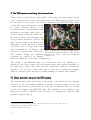
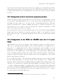
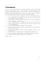
Under a silver-coloured bracket in the middle of the main board (main printed circuit
board – main pcb) there is the wafer as the heart of the WSI system (cf. figure 1). On
the wafer there are 48 reticles3, each of them consisting of eight HICANN4 chips, which
contain the neuron and synapse circuits
as actual electronic images of the
biological system [5]. In the human brain,
information processing takes place via
electrical signals between the brain cells –
the neurons. These electrical signals arise
from potential differences between the
inside and the outside of the neuron cells.
Surpassing a voltage threshold, a neuron
can emit a spike, a voltage peak, which
will be transmitted to, for instance, other
Figure 1: Wafer Scale Integrated (WSI) System.
neurons or to muscle cells in the body. The Wafer is situated under the silver-coloured
The currents driving the membrane bracket in the centre – taken from BrainScaleS
potentials are controlled by channels, homepage [34].
which are regulated by each other’s conductivity [6].
The circuits of the HICANN chips now work in the same way: Making use of
transistors’ low voltage resistive area’s exponential drain-source current dependency on
the drain-source voltage, they cause the same conductance behaviour as membrane
currents do. To be able to achieve this, they of course need a certain power supply,
which is controlled by the clkboard programme running on a single board computer.
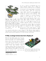
2.1 Basic
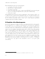
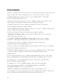
asic technical setup of the WSI system
The wafer mounted under the bracket in the middle of the main board is electrically
connected to the surrounding periphery by flexible electrical contacts. In the four
corners of the main pcb powerboards and clockboards are installed. They are essential
for the power supply of the HICANN chips. The remaining boards, installed on the
main pcb as well, are FPGA5 boards, necessary for communication with the WSI
system (cf. figure 2 and [5]).
3
4
5
A reticle is the largest structure possible to manage during one production step of the wafer [5].
High Input Count Analogue Neural Network.
Field Programmable Gate Array.
2
2 The WSI system emulating the human brain
In order to function, the HICANN chips need
twelve different voltages. Ten of them are
generated on the powerboards, the two remaining
are provided by an external supply, as they may
need high currents, which the powerboards
cannot supply. From these power supplies the
voltages are routed to the HICANN chips
through the main pcb. The monitoring of the
voltages is conducted by 24 microcontrollers6
situated on the main pcb, each of the
microcontrollers monitoring the voltages of two
Figure 2: Model of WSI system reticles. The circuits delivering the voltages
composition. From bottom to top:
contain FETs7, which are needed to switch the
Cooling fins, wafer with bracket, main
printed circuit board (main pcb), four voltages on or off. The FETs can either close the
FPGA boards5. The FETs7 necessary to circuits to apply the voltages or open the circuits
gate the supply voltages are situated
to disconnect the voltages. There are measuring
under the bracket in the middle, the
PICs6 are the 24 small black squares points before and after the FETs, the values of
distributed in the corners of the main which are monitored by the corresponding
pcb.
(Taken
from
the
WSI
microprocessor. If the values surpass a certain
documentation [5].)
threshold, the microcontroller switches the FETs
off, so that the reticles have no more voltages [5]. The different voltages applied to
each reticle can be switched on and off manually as well, for instance when starting the
system. At this point the Raspberry Pi becomes relevant for the system.
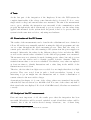
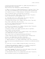
2.2 Why to exchange the former board with a Raspberry Pi
When the first WSI system was set up two
years ago, the CPU8 module chosen to run the
clkboard programme was a taskit Stamp9G20.
The processor comes along with an evaluation
board, which provides interfaces necessary to
communicate with the other parts of the WSI
system. Today, this hardware setup is
somewhat outdated. There are faster processors
with a smaller periphery, which still provide all
required interfaces and which are at the same
time less expensive. One of the best total
6
7
8
Figure 3: Raspberry Pi – size as big as a
credit card. The header P1 is the one at
the very left, equipped with pins. This
header is used with the ribbon cable.
dsPIC33FJ128GP710 - „PIC“.
Field Effect Transistor.
Central Processing Unit – „processor“.
3
2 The WSI system emulating the human brain
packages is provided by the Raspberry Pi (cf. figure 3), originally designed by the
Raspberry Pi Foundation to “[promote] the teaching of basic computer science in
schools”. [7] [8] The table below lists some of the technical details of both of the boards
and shows, why a change is reasonable [9] [10] [11] [12].
taskit Stamp9G20 with
Evaluation board
Raspberry Pi Model B
Chip
Atmel® AT91SAM9G20
Broadcom BCM2835
CPU
400 MHz ARM
700 MHz ARM
Coprocessors
--
digital processing, floating point
unit
GPU
--
Dual Core VideoCore IV®
Multimedia Co-Processor
Memory
64 MB SDRAM (optional up
to 128 MB)
512 MB SDRAM
Ethernet, USB
10/100 Mbit/s Ethernet
10/100 Mbit/s Ethernet
Power Supply
3.3 V
5 V MicroUSB
Power
Consumption
max. 180 mW
max. 3.5 W
Dimensions
20 cm x 13 cm x 4.5 cm
8.6 cm x 5.4 cm x 1.7 cm
Price
299 EUR [10]
~ 40 EUR [12]
Table 1: Comparison between taskit board and Raspberry Pi. The latter is faster, smaller and
cheaper than the former.
The communication between the Raspberry Pi and the rest of the system runs by a
ribbon cable. A further advantage of the Raspberry in comparison to the taskit board
not listed in the table is its huge community providing support and many projects
already carried out with the Raspberry Pi. This often facilitates finding solutions for
problems occurring when operating a Raspberry Pi.
2.3 The Raspberry Pi’s tasks
tasks in the system
Enabling users to switch on and off the FETs for single reticles is only one task of the
clkboard programme. In fact, the overall task of the programme is to provide an
interface to the whole power supply chain which allows comprehensive monitoring and
control. Running on the Raspberry Pi it provides a handy interface, which bundles all
further interfaces necessary to manage the WSI system power supply and requires only
Ethernet to be accessible.
4
2 The WSI system emulating the human brain
A future aim with regard to the WSI system and especially with regard to the clkboard
programme and the Raspberry Pi is further automation. One command should be
enough to start the whole system, monitoring should work independently from constant
human supervision and above all, it should react to certain critical values by itself as
for instance to temperatures which surpass a certain threshold. As the plans for the
whole project include several WSI systems running in parallel, large-scale automation is
absolutely necessary. This can be further elaborated after the integration of the
Raspberry Pi.
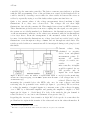
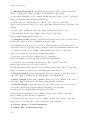
2.4
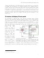
2.4 Interfaces,
nterfaces, the Raspberry Pi has to provide
The performance of different tasks of the clkboard programme requires different
interfaces to the WSI system, which the Raspberry Pi has to provide. These interfaces
are two I2C9 busses, one 1-wire bus and three GPIO10 busses so far (cf. figure 4). The
GPIO busses pass the HICANN reset signal, which resets all HICANNs to a certain
standard configuration and the enabling signal for the external 1.8 V power supply.
The 1-wire bus is used for temperature readout. One of the I2C busses accesses the
microcontrollers which
monitor
the
FET
voltages (cf. figure 4:
I2C-0 to PICs), and the
other one accesses the
powerboards for data
readout (cf. figure 5:
I2C-1 to PSB). The
separation of the two
I2C busses was carried
out because of security
considerations, so it will Figure 4: Schematic diagram of the interfaces between the Raspberry
still be possible to Pi and the main pcb. User access to the programme takes place
switch off the voltages, through Ethernet. The different commands executable from within
the programme require different interfaces to the WSI system.
if one of the busses is
blocked completely due to, for instance, a defect of the adherent devices [5] [13]. In the
following, short overviews over the functionality of the used interfaces are provided.
9
10
Inter-Integrated Circuit.
General Purpose Input/Output.
5
2 The WSI system emulating the human brain
2.4
2.4.1 Overview I2C
Developed in the 1980s the I2C bus has evolved to one of the most frequently used
busses in inter-circuit communication. Its architecture follows the master-slavearchitecture, which means that one master device controls several slave devices. Slaves
can never read or write data on their own. The I2C bus is a two wire serial bus, using
one wire for the clock (SCL) and the other one for data (SDA). To start
communication the master device sends a start signal in such a way that the data line
switches from high potential (“high”) to low potential (“low”), while the clock line
remains high (cf. figure 5). Switching SDA while SCL remains constant is only allowed
for the start and stop signal. For data transfer SDA has to remain unchanged while a
clock pulse is being sent. The stop signal works in the opposite way of the start signal,
so SDA switches from low
to high while SCL remains
high (cf. figure 5). Data
transfer takes place in
between these two signals.
After the start signal, the
Figure 5: Schema of start and stop sequence for I2C
communication. Only for these two signals SDA is switched master device sends the
while SCL remains constant. Data transfer takes place in address of the device it will
between these two signals. (Taken from http://www.robot- communicate with, so that
electronics.co.uk [45].)
the other slaves will not be
affected. After the address has been sent, communication will begin. The master device
can determine, if it will write data to SDA to be read by the slave or if it will read
data sent by the slave. In order to confirm that the transfer of one byte of data has
been successful, the receiving device will send an acknowledgement signal to avoid data
loss in case of unsuccessful communication [14].
Typical clock frequencies for I2C communication are up to 100 kHz in standard mode,
up to 400 kHz in fast mode or even up to 3.4 MHz in high-speed mode. To transfer a
single bit, SDA switches to low or high, depending on whether a 0 or a 1 is to be
transferred and while SDA remains constant, the bit is transferred by the clock
switching from low to high and back to low again – this is one clock pulse [14].
The I2C communication can be observed on an oscilloscope by simply connecting the
oscilloscope inputs with the two I2C lines. During this thesis observations of the signals
have been conducted to test, if higher clock frequencies than 100 kHz can be used for
communication and to look for communication errors. These tests will be shortly
discussed later on.
6
2 The WSI system emulating the human brain
2.4
2.4.2 Overview 1-wire
1-wire busses in contrast to I2C busses use only one communication line. The fact that
no clock signal is transferred during communication requires the definition of another
kind of consistent timing. Similar to the I2C bus, the 1-wire bus is based on the
master-slave-principle, so consistent timing is achieved by passing bits every time the
master signal reaches a falling edge11. Transferring 0 or 1 is implemented by the use of
different times, during which the line is pulled to low potential. Using only one line and
thus a different communication protocol 1-wire does not reach communication speeds
as high as I2C – standard mode reaches up to about 16 kHz whereas overdrive mode
may reach up to about 140 kHz [15].
1-wire is often used to monitor sensors such as temperature sensors, which is exactly
how it is used in the WSI system. Overall, there are six temperature sensors integrated
into the central system (main pcb plus clockboards and powerboards, cf. figure 2) so
far: four of them situated immediately under the wafer bracket (cf. figures 1 and 2) to
measure the wafer temperatures during runtime and two more sensors outside of the
bracket to measure room temperatures. More temperature sensors can be found on the
boards attached at a later stage, but they are monitored in a different way [5].
2.4
2.4.3 Overview GPIO
General Purpose Input/Output (GPIO) pins can be used – as the name implies – for
many different purposes. It is possible, for instance, to use GPIO pins for I2C or, if
programmed appropriately, simply for switching a device on or off by applying or
removing a potential. These two tasks are exactly the two, which the Raspberry Pi’s
GPIO pins are used for in the WSI system. Using a GPIO pin only requires defining it
as input or output pin and sometimes connecting it to a pull-up resistor12, so that it
does not need to be driven by the chip. [9]
In the WSI system the used GPIO pins are all defined as output pins. One can be used
to execute a HICANN reset, if necessary, another one switches the 1.8 V power supply
on or off (cf. figure 4).
11
Edge: Signal switching from high to low (falling edge) or from low to high (rising edge).
A pull-up resistor ensures that the pin potential (logic level) is driven towards a certain value determined by the
pull-up resistor and an external voltage supply. This is necessary when devices connected to the chip require higher
power than the chip is able to deliver.
12
7
3 Execution of the integration
integration
This chapter describes the actual steps that were carried out to successfully integrate
the Raspberry Pi into the WSI system. A step-by-step guide of the setup for practical
use can be found in the clkboard gitviz wiki and is also included in the addendum.
To comply with the WSI system requirements the following steps have to be carried
out:
•
•
•
•
setting up an operating system for the Raspberry Pi to be able to run the
clkboard programme;
adapting the pin layout of the Raspberry Pi GPIO header in the kernel to
match the clockboard pin layout (cp. figures 6 and 7);
configuring the interfaces used for the communication with the WSI system;
adapting the clkboard programme from the taskit board to the Raspberry Pi.
(This had to done only once which happened during the work on this thesis.)
3.1 Installation of the operating system Debian
The clkboard programme is laid out to run on top of an operating system, so installing
one on the Raspberry Pi is the first thing to do. The preferred system for this task is
Debian, as there is a distribution available, which is optimised in particular for the
Raspberry Pi. It can be downloaded from
http://www.raspberrypi.org/downloads [16].
For this thesis the “Wheezy 2013-02-09” distribution was used. The operating system
always runs from an SD card, which was found to be reasonable during the
development of the Raspberry Pi. SD cards deliver high capacity, are cheap and fast,
easily writable and easily changeable in case of damage. The link provided below13
contains a table with reportedly working SD cards and read/write speeds.
The size of the used card should amount to at least 4 GB, as it will contain the
operating system (about 2 GB) and should still provide some additional space. The
filesystem used for the first setup during the integration of the Raspberry Pi into the
WSI system was ext4 [17]. It is recommended to continue working with ext4 or at least
another journaling filesystem, as journaling provides higher security in case of a power
failure or a system crash [18]. After unpacking the downloaded Debian image, it can be
copied onto the SD card [19]. (Cf. step-by-step guide for details of the SD card setup.)
13
8
http://elinux.org/RPi_SD_cards [50]
3 Execution of the integration
If connected to a monitor, booting the Raspberry Pi with its new operating system for
the first time should display a configuration menu. In case of not using an extra
monitor for the Raspberry Pi (but using e. g. SSH14 instead) the configuration menu
can be accessed with the help of the command raspi-config (as root). One should at
least expand the file system on the SD card to be able to use all of its space. (Cf. stepby-step guide for further properties.)
3.2
3.2 Preparation of the kernel for the clkboard programme
The central unit of an operating system is its kernel, which is situated between the user
software and the hardware and manages access to the hardware. The Debian Wheezy
distribution is based on a Linux kernel,
which is maintained as open source
project [20].
As the kernel is responsible for managing
hardware access, it also defines which
pin is available for which functionality.
Therefore, the kernel has to be
configured in such a way that it fulfils
the requirements of the clockboard pin
layout (cf. figure 6). This guarantees
that the hardware is supported by the
operating system in an optimal way.
The Raspberry Pi provides five headers Figure 6: Pin layout for the ribbon cable adapter
on the clockboard. This layout defines which pin
with accessible pins. They consist of 26, has to be configured for which clkboard
eight, another eight, seven and two pins programme function. The blue circle is a drill hole
and mostly act as GPIO pins. Two of in the corner of the board [48].
the headers are used as JTAG15 interfaces during the production of the board. The
header of main interest is the so called P1 header, which is also the only header
equipped with connectors. Some of its pins are preconfigured, two of them already in
the way it is required by the clockboard layout (cp. figure 6 and 7). All of the pins can
be used as GPIOs [21].
In chapter 2.4 the required functionalities have been described already. Figure 6 shows
which pin has to provide which functionality. From the Raspberry Pi github, a Linux
kernel for further configuration was cloned. The clone directory was
https://github.com/raspberrypi/linux.git [22].
14
15
Secure Shell – Network protocol.
Joint Test Action Group – interface for debugging purposes.
9
3 Execution of the integration
Necessary adaptions take place in the bcm2708.c file, which contains information about
the pin configuration. In the cloned directory it can be found in the
linux/arch/arm/mach-bcm2708 subdirectory. With regard to the pin layouts shown in
figure 6 and 7, the following changes have to be carried out:
•
•
W1_GPIO 14 instead of W1_GPIO 4 for 1-wire;
UART0_DMA { 22, 25 } instead of UART0_DMA { 15, 14 } to avoid
overwriting the 1-wire pin definition.
GPIO 0 and GPIO 1 are already correctly defined as I2C interface pins (cf. figure 7).
Another aspect, which does not concern pin definitions but which is a prerequisite for
configuring the second I2C bus later on, has to be taken care of at this point. In the
kernel’s .config file the CONFIG_I2C_GPIO option
has to be set to CONFIG_I2C_GPIO = m in the
line already predefined. This makes it possible to add
the I2C module, which will be responsible for the
second I2C bus, at a later stage.
When the pin layout and the CONFIG_I2C_GPIO
option have been changed in the bcm2708.c file, the
kernel has to be compiled and moved to the /boot
directory, so that the Raspberry Pi will use the new
kernel and the new pins accordingly when it boots.
(Cf. step-by-step guide for details.)
A common way to compile Linux kernels is cross
compilation. This allows compilation on a host system
with much more processing power than the target
system can provide. Its realisation requires a systemspecific cross compilation toolchain, which ensures
that the executable files created on the host system
are actually executable on the target system. Such a
toolchain is necessary because the host processor and
the target processor are based on different processor
architectures, which differ in their instruction sets16. Figure 7: GPIO pin numbering on
the Raspberry Pi P1 header [21].
In this case the host processor is based on the x86
architecture17 [23] [24], whereas the target processor is based on the ARM architecture18
[25].
16
17
18
Most basic operations, a processor can execute.
Developed by Intel. Cf. referenced documents for further information.
ARM – Advanced RISC Machine; RISC – Reduced Instruction Set Computing.
10
3 Execution of the integration
Building a cross compilation toolchain was the first approach to compiling the custom
Linux kernel. crosstool-ng [26] promised to be an easy way to set up such a toolchain,
thus, using this programme was the first try. Following for instance the guide on
http://www.kitware.com/blog/home/post/426 [27] should have led to a toolchain
ready to compile the kernel. Unfortunately, even after several attempts and
consultation of as well as practical help by experienced programmers within the
research group it was not possible to set up a working toolchain on the used host
system. Some host system modules caused dependency problems, which could neither
be resolved automatically by using apt-get install nor manually by trying to install the
modules one by one. To avoid further unnecessary delay it was decided to continue
compiling on the Raspberry Pi itself. This option was not favoured in the first place, as
it requires some time. To lose as little time as possible the compilation was started to
run over night. As it turned out, it takes about six hours to complete the kernel
compilation on the Raspberry Pi itself. Altogether, compilation took place some three
or four times during the work on the system, so the solution of using the Raspberry Pi
for compilation and running the compilation over night could be considered as
reasonable afterwards.
3.3
3.3 Configuration of the required interfaces
interfaces
In chapter 2.4 the tasks of the required interfaces were already discussed. As stated
there, the following interfaces need to be configured:
•
•
•
•
two I2C interfaces for access to the PICs and the powerboards;
one 1-wire bus for temperature readout;
one GPIO pin for the HICANN reset;
two further GPIO pins, one of them for the external 1.8 V power supply, the
other one not used yet.
The pins were already defined in the chapter above, when the compilation of the kernel
was executed, so in the following only the necessary software adaptations are explained.
3.3
3.3.1 Configuration of the I2C busses
The Raspberry Pi provides two I2C interfaces ex factory, where one of them is on the
“wrong” header – on header P5, which will not be used by the ribbon cable. Of course,
one could change the cable and direct single pins to the other header, but this would
not be as handy and usable as a single plug for the cable. So a second I2C interface was
configured on the P1 header using a bit-banging19 module developed by Krzysztof A.
19
Bit-banging describes the emulation of a hardware interface with the help of software and GPIO interfaces.
11
3 Execution of the integration
Adamski, a developer from the Raspberry Pi community. The Raspberry Pi even has a
pull-up resistor embedded for some pins [21], so that only for the added interface an
external pull-up resistor had to be soldered onto the clockboard.
For the first I2C bus only the corresponding drivers provided by the operating system
have to be activated. This happens by removing the drivers from the modprobe
blacklist20 and adding them to the /etc/modules file, so that they are loaded
automatically when the Raspberry Pi is booted. (Cf. step-by-step guide for details.)
The Raspberry Pi I2C bus is capable of communicating with at least 400 kHz, but
unfortunately some of the voltage values were transferred incorrectly when using a 400
kHz clock21. To implement the second I2C interface, the kadamski module22 mentioned
above was used.
The addition of further I2C busses using the kadamski module is realised with the help
of Linux’s platform devices. These provide methods to inform the kernel about
hardware, which it cannot detect on its own [28]. The kadamski module works as an
I2C bus driver, so it provides a struct, which the kernel is able to identify as device.
Platform device drivers recognise actual devices, the device names of which match the
ones given to the driver, for instance via an ID table. Once a driver recognises
matching device names, it will attach to the device and henceforth manage
communication with this device [29].
Activating the kadamski module, so that it can be used, is basically done in the same
way as adding any c programme. The module can be downloaded from
https://github.com/kadamski/i2c-gpio-param [30].
Afterwards it just has to be compiled and the result has to be moved to the
kernel/drivers directory. Then it can be loaded automatically at boot time, when the
command to do so is added to the /etc/modules file. When loading the module a
default bus is being initialised. In this case, where the pins for the additional I2C bus
are known from the beginning and where they are fixed and will not change, the
default bus and its pins can be specified before compiling. As a consequence the module
only has to be started and it is not necessary to remove the default bus and to add the
correct bus.
Before testing the I2C busses within the WSI system both of them were tested with a
chain of temperature sensors. All sensors were recognised by the busses and the
temperature values could be read.
20
Modules included in the modprobe blacklist are prevented from being loaded automatically during the booting
process.
21
Cf. chapter 4 for further information.
22
As the developer’s username is kadamski the module will be referred to as kadamski module in the following.
12
3 Execution of the integration
Note that the I2C busses used in the clkboard programme are called I2C-0 and I2C-1
whereas the busses used on the Raspberry Pi are called I2C-1 and I2C-2. The reason
for this is that the I2C-0 bus on the Raspberry Pi is the one on the P5 header, which is
not used.
3.3.2
3.3.2 Configuration
Configurat ion of the 11-wire bus for temperature readout
As the operating system provides drivers for 1-wire and also for temperature readout
via 1-wire the only thing that had to be done apart from loading the drivers was
specifying the pin, which is to be used, in the corresponding kernel file. This has
already been taken care of when compiling the kernel. To enable the drivers at boot
time they have to be added to the /etc/modules file, which is responsible for this
action. (Cf. step-by-step guide for details.)
Before testing the 1-wire bus in the WSI system, it was tested with a single DS18B20
temperature sensor, which was soldered together according to its datasheet [31] and
then connected to the corresponding GPIO pin. There were no problems when testing
the bus.
3.3
3.3.3 Configuration of the GPIOs
GPIO s for HICANN reset
reset and 1.8 V power
supply
The HICANN reset and power supply control interfaces require one GPIO pin each.
There is no operating system support for the required functions (cf. chapter 2.4), so
they had to be implemented in the clkboard programme. One possibility to access
GPIO pins on the Raspberry Pi was found on the internet [21] and adapted to the
specific needs of the Raspberry Pi in the WSI system. Access takes place with the help
of the operating system’s memory device file23. Byte addresses passed to this file are
mapped to physical memory addresses which allows direct manipulation of the GPIO
pins via their memory addresses.
In one of the header files of the clkboard programme some macros were defined, which
use the GPIO pin number on the pin header on the Raspberry Pi to calculate the
memory address for the pins. If something in the programme will be changed later on it
will have to be taken into account that the GPIO number (cf. Figure 6) has to be used
– not the continuous pin number beginning with 1 in the bottom left and ending with
26 in the top right [21]. When compiling the kernel, it has already been taken care of
that the pins needed for HICANN reset and power supply switch will not be occupied
by some Raspberry Pi internal functions.
23
/dev/mem – short description on http://linux.about.com/library/cmd/blcmdl4_mem.htm [42].
13
3 Execution of the integration
When initialising the pins, the following happens:
•
•
•
•
•
open memory device file /dev/mem;
map addresses to physical memory;
close memory device file;
define pin as input using a macro defined in the HICANN reset header file (pins
have to be set always as input first due to pin register definition [21]);
define pin as output.
After initialisation the pins can be used as output pins, so they can pass a value 1 or 0
to adherent devices. Apart from the initialisation there are two functions which access
exactly the pins defined in the clockboard layout. These two functions are integrated
into the clkboard programme menu, so they can be called using the predefined
commands when the programme is running.
3.4 Compilation of the clkboard programme
Once the new functions for GPIO access have been defined and added to the menu file,
the programme had to be compiled for the Raspberry Pi. From previous compilations
for the taskit board it was known that the compiling and especially the linking takes
some time, mostly due to RCF24 libraries [32] used in the programme. So the idea was
again to use cross-compiling, although its setup would be a little tedious. Unfortunately
again – as when trying to cross-compile the kernel – some errors occurred that could
not be resolved immediately. It took some fruitless effort, until Eric Müller came up
with a quite handy trick: On the internet he ran into a way to emulate a Raspberry Pi
on a host computer, but in a way that emulates only the instruction set instead of the
whole Raspberry Pi. It is based on qemu, a processor emulation programme [33]. Using
this method saved a lot of resources and made it possible to reduce compiling and
linking time from at least 20 minutes on the Raspberry Pi to about five to ten minutes
on a desktop PC. (Cf. guide in the addendum for how to set up the qemu
environment.)
24
Remote Call Framework - cross-platform interprocess communication framework for C++ [32].
14
4 Tests
As the last part of the integration of the Raspberry Pi into the WSI system the
complete functionality of the voltage control interface had to be tested. To do so, every
single reticle’s voltage and current values were measured. The aim of the measurement
was to prove, whether the integration was successful, if the communication works
properly throughout the whole system and to get an overview over the values being
applied and measured by the system itself. In general, it had to be proven, that the
system is in the same state as before, only using new hardware.
4.1 Examination of the I2C busses
The results of the measurements can be found in the addendum and were obtained as
follows. All reticles were manually switched on using the clkboard programme and only
one at a time throughout the whole measuring process. Then, first, the value of a
current probe attached to the cable running to the system from the power supply was
measured. Afterwards, the values for the different voltages before and after the FETs
as well as the current values calculated by the clkboard programme were measured.
The measures were not orientated towards obtaining precise values, but only to get an
overview over the reticles and to identify possibly defective elements. Thus, no
statistical mean values or errors were calculated. Nevertheless, every value was updated
at least ten times to identify fluctuations and a value lying in the middle of the
fluctuations was noted down.
Therefore, the fact that four digits were recorded does not imply that there is a high
precision. They were noted down in such a detail nevertheless, because it was
interesting to get an insight into the fluctuations and to obtain a distribution of
current values for the more stable voltages.
As mentioned in chapter 3.3.1, some of the voltage values were transferred incorrectly
when the I2C bus was driven by a 400 kHz clock. For some of the values only half of
their actual value was displayed. If a clock of 100 kHz is used, all values are transferred
correctly.
4.2 Analysis of the I2C measurement
First and most important of all, the results prove that the integration has been
successful. All reticles could be accessed, switched on and off and their values could be
obtained. Six of the 48 reticles showed strange behaviour25, two of them being
25
Cf. comments in tables 2.1 and 2.2 included in the addendum.
15
4 Tests
controlled by the same microcontroller. The latter occurrence may indicate a problem
with the PIC programming. None of the problems were caused by the Raspberry Pi as
could be shown by observing correct values for other reticles in between the errors as
well as by repeatedly trying to read the faulty values again some time later on.
Quite a few current values of the voltage measurement showed medium to high
fluctuations. If so, they were colour-coded26. The voltages did not show high
fluctuations, but only the currents did. This simply derives from low FET resistances.
These fluctuations probably arise from noise coupling into the signal, as some parts of
the system are not ideally insulated yet. Furthermore, the fluctuations seem to depend
on the measurement conditions, as the values were measured with far less fluctuations
a few days later27. From the arrangement of the measured values in the table it
becomes obvious that the fluctuations are voltage based and not reticle based, as the
fluctuations occur throughout voltage columns and not throughout reticle lines. The
reticles provided with error annotations will be investigated during work going beyond
this thesis.
Current values being
calculated as negative
derive from suboptimal
measurement points. To
measure
all
twelve
voltages of a reticle, two
reticles
per
microcontroller, 48 inputs
would be required. As one
PIC provides only 32
inputs the total inputs
Figure 8: Ways to reduce the number of required PIC inputs to needed for the monitoring
measure the voltages dropping over the FETs. (Taken from the WSI of all voltages have to be
documentation [5].)
reduced. This is done by
measuring the potential before the FETs only once for some voltages and thus
retrieving only one potential for two reticles (cf. figure 8 – grey lines). The second way
to reduce the number of required inputs is to measure some of the voltages dropping
over a FET by a differential amplifier and passing the amplifier’s output to a PIC
input pin (cf. figure 8 – black lines). For both of the methods, the pin demand is
reduced from two to one, but to the detriment of less precise data [5].
Regarding the incorrect data transfer at high I2C clock speeds it seems that the
problem has its origins in the transfer of the values and not in the values themselves. It
26
27
Cf. table 1 for an explanation of the colours.
This was not a part of this thesis, which is why the results are not part of the addendum.
16
4 Tests
could be possible that a bit-flip occurred due to too high speed, which could explain the
occurrence of exactly half of the actual value. Unfortunately, there was no time left to
investigate this any further. The next steps would be examining the I2C signal with an
oscilloscope to identify the source of the error. Additionally the speed of the I2C clock
could be raised gradually to find the threshold, above which the values are transferred
incorrectly.
The explanations given for fluctuations or for negative values are only supposed to
supply hints on what has to be taken into account when examining the measurement
results. They are not intended to sufficiently explain existent deviations from optimal
values28. This is because it was not the purpose of the measurement to quantitatively
analyse imperfections in the WSI system setup, but rather to check on communication
between the Raspberry Pi and the system.
28
Cf. comments in table 1: The optimal values were defined in the context of the design of the system.
17
5 Conclusion
By successfully addressing every single reticle on the wafer, it has been established that
the integration of the Raspberry Pi into the WSI system was successful as well. This
means that the system is in the same state as before, even better, as it uses new
hardware. The decision to use a Raspberry Pi instead of the former taskit evaluation
board turned out to be – as expected – a good idea. The Raspberry Pi is faster,
smaller, cost-efficient and easy to handle. As mentioned in chapter 2.2 there is also a
huge Raspberry Pi community, which was already to the benefit of the integration into
the WSI system. Using the kadamski I2C bit-banging module very much facilitated
adding a second bus to the required header. It will also facilitate changes to the system
in future, as the busses can be added dynamically using almost every GPIO pin
available. A guide on how to do so is included in the addendum and can be found on
the gitviz page as well.
It would have been worthwhile to further investigate the 400 kHz I2C clock and to fix
the incorrect data transfer, but there was no time to do so. Nevertheless, it seems that
communication at high-speed using 400 kHz is only a few steps away. Achieving
successful use of a 400 kHz clock would of course reduce a possible bottleneck and
increase security.
A new feature accompanying the inclusion of the Raspberry Pi into the WSI system is
the possibility of switching on the whole system with just one command. Concerning
this feature, the most decisive addition is the GPIO pin accessing the 1.8 V power
supply. With the former power supply this would have been possible as well – but it
was not done so far, because it would have taken too much time. The use of the new
1.8 V power supplies being introduced with the new system will be maintained,
avoiding the necessity to buy more of the unhandy power supplies used so far, because
the new power supplies are designed by the Electronic Vision(s) group.
Furthermore, now there is a detailed, modularised and easy-to-follow workflow, which
allows changing present and adding further features to the Raspberry Pi and the
clkboard programme. Creating this workflow and the annexed guide29 is an important
result of this thesis. As it describes the complete Raspberry Pi setup, it includes
compiling the Raspberry Pi kernel, which is important for further hardware changes
and it also includes compiling the clkboard programme, which is of course important
for further software changes. The workflow was tested several times, partly also on
different PCs, so future developers can simply follow it – even without basic knowledge,
29
Cf. 9.2 step-by-step guide.
18
5 Conclusion
as the guide was explicitly written in a way, that not only experts but also beginners in
this field can work with it.
The work on the Raspberry Pi itself allowed first insight into hardware programming
and even a little more insight into the possibilities and the importance of using Linux
in a scientific environment. Getting to understand the WSI system at hardware level
alone took quite a while and yet, it was only possible to scratch the surface, which
shows the system’s immense complexity. Nevertheless, it was very interesting and the
work on this thesis was always challenging and most of all very instructive.
Figure 9: Comparison between the new and the old board. Raspberry Pi on the left side with a
ribbon cable running to one of the clockboards, USB power supply and Ethernet cable; former
taskit board (not connected anymore) on the right – clearly visible size difference.
19
6 Outlook
There are some features connected to the Raspberry Pi in the WSI system, which can
and will be improved in future. Maybe the greatest issue is time, as many possible
starting points are known, however, the necessary manpower is not available. The
possibility of using a 400 kHz bus for the communication between the PICs on the
main pcb and the Raspberry Pi is the most obvious aspect connected to the Raspberry
Pi. Second, the noise coupling into the voltage signals, which was observed during the
communication test, will be reduced permanently sooner or later by proper insulation.
Another aspect, which is already being dealt with, is a possible redesign of the main
pcb in such a way that it will be possible to directly measure all potentials before and
after the HICANN FETs instead of using differential pairs or measuring the potential
for adjacent FETs on a single line. This will increase measurement stability.
Furthermore, some automation could be introduced, for example regarding
measurements presently done by hand. A suitable programme just needs to read the
voltage values several times, calculate a mean and a standard deviation to observe
fluctuations and should possibly include some security functions to switch off FETs in
case of high currents. As stated in chapter 2.3 several automation processes with regard
to starting, stopping and monitoring the whole WSI system are also necessary and will
be implemented. The Raspberry Pi, providing newer and faster hardware than the
former taskit board, offers solid conditions in this context. What is needed above all
also for other issues is time, which is scarce. Some of the issues at stake might be
suitable for internships.
A second Raspberry Pi has been configured in the same way as the first one, so it can
be integrated into the first WSI system, which is already running, soon. Then the
taskit board will not be needed anymore in neither of the systems. The second WSI
system, into which the Raspberry Pi has been integrated during this thesis, will be
completed in the near future using the Raspberry Pi as power supply interface and –
together with the further systems to come – will be bringing research closer to the
understanding of the human brain.
20
7 Acknowledgements
Acknowledgements
At the end of this thesis I would like to express my gratitude to several people for their
support in many different ways. I could never have come this far without those
supporting me and thus I would have never been able to reach the end of my studies in
the field of physics. This thesis as the conclusion of my studies seems a good place to
write down my greatest thanks. (In random order) I am deeply grateful to
•
•
•
•
•
•
•
•
•
above all my parents and my grandparents for their love and understanding, for
always supporting me through word and deed and for their absolute
encouragement for whatever I plan to do;
my brother, my sister and my friends for being there for me and making the
world a bright place every single day;
Professor Karlheinz Meier for admitting me into the research group and for
leaving a lasting impression on me already in the first two semesters (lectures
on experimental physics);
Doctor Johannes Schemmel for being my second examinant;
Maurice Güttler for ever patient support and explanations during my bachelor
thesis and my internship;
Eric Müller for frequent IT assistance and for presenting a solution to every
problem possible;
Alexander Gorel for reading my bachelor thesis and giving valuable advice.
the whole Electronic Vision(s) group for a friendly and helpful environment;
others whom I have unintentionally omitted from this list.
Thank you all!
21
8 List
List of references
Websites occurring in the list of references are listed the following way: Side name, site
name, possibly date of last actualisation, date of last visit on the site, address.
1. Human Brain Project. Human Brain Project. [Online] [Cited: 7 July 2013.]
http://www.humanbrainproject.eu/.
2. Electronic Vision(s). Electronic Vision(s). [Online] 14 May 2015. [Cited: 7 July
2013.] http://www.kip.uni-heidelberg.de/cms/groups/vision/home/.
3. In Brief. Blue Brain Project. [Online] 29 April 2013. [Cited: 7 July 2013.]
http://bluebrain.epfl.ch/page-56882-en.html.
4. The FACETS Neuromorphic Hardware. Electronic Vision(s). [Online] 19 May 2011.
[Cited: 7 July 2013.] http://www.kip.uniheidelberg.de/cms/vision/projects/facets/neuromorphic_hardware/.
5. Husman de Oliviera, Dan, et al., et al. FACETS Wafer-Scale Integration
(WSI). Heidelberg, Dresden : s.n.
6. Gerstner, Wulfram and Kistler, Werner M. Spiking Neuron Models.
Lausanne : Cambridge University Press, 2002. ISBN 0 521 81384 0 : 90 USD .
7. Raspberry Pi. Wikipedia. [Online] 4 July 2013. [Cited: 7 July 2013.]
http://en.wikipedia.org/wiki/Raspberry_Pi..
8. About. Raspberry Pi. [Online] Raspberry Pi Foundation, 2012. [Cited: 7 July 2013.]
http://www.raspberrypi.org/about.
9. BCM2835 ARM Peripherals. Raspberry Pi Center. [Online] Broadcom, 2012. [Cited:
7 July 2013.] http://raspberrycenter.de/sites/default/files/bcm2835-armperipherals.pdf.
10. Price List Stamp9G20. taskit. [Online] taskit GmbH, 2012. [Cited: 7 July 2013.]
https://ssl.kundenserver.de/ssl.taskit.de/xtc/product_info.php?products_id=271.
11. Raspberry Pi. farnell. [Online] Farnell, 2007 - 2010. [Cited: 10 July 2013.]
http://de.farnell.com/raspberry-pi.
12. Raspberry Pi. amazon. [Online] Amazon, 2013. [Cited: 10 July 2013.]
http://www.amazon.de/Raspberry-Pi-RBCA000-Mainboard-1176JZFS/dp/B008PT4GGC/ref=sr_1_1/278-46088452407944?ie=UTF8&qid=1373470085&sr=8-1&keywords=Raspberry+Pi.
13. sw-wsiclkboard. gitviz BrainScaleS Repository. [Online] 2013. [Cited: 7 July 2013.]
https://brainscales-r.kip.uni-heidelberg.de/projects/sw-wsiclkboard.
22
8 List of references
14. I2C-bus specification and user manual. nxp. [Online] nxp Semiconductors, 13
February 2012. [Cited: 7 July 2013.]
http://www.nxp.com/documents/user_manual/UM10204.pdf.
15. iButton. maximintegrated. [Online] Maxim Integrated, 7 April 2005. [Cited: 7 July
2013.] http://www.maximintegrated.com/products/ibutton/ibuttons/standard.pdf.
16. Downloads. Raspberry Pi. [Online] Raspberry Pi Foundation, 9 February 2013.
[Cited: 22 April 2013.] http://www.raspberrypi.org/downloads.
17. Main Page. Ext4 Wiki. [Online] Linux, 21 June 2013. [Cited: 7 July 2013.]
https://ext4.wiki.kernel.org/index.php/Main_Page.
18. Journal File System. Linux. [Online] Linux, 2013. [Cited: 7 July 2013.]
http://www.linux.org/article/view/journal-file-system.
19. RPi Easy SD Card Setup. elinux. [Online] 6 May 2013. [Cited: 7 July 2013.]
http://elinux.org/RPi_Easy_SD_Card_Setup.
20. About. linux. [Online] Linux Foundation, 2012. [Cited: 10 July 2013.]
http://www.linuxfoundation.org/about.
21. RPi Low Level Peripherals. elinux. [Online] 4 July 2013. [Cited: 7 July 2013.]
http://elinux.org/RPi_Low-level_peripherals.
22. Raspberry Pi Linux. github. [Online] April 2013. [Cited: 25 April 2013.]
https://github.com/raspberrypi/linux.
23. Intel Architecture Software Developer's Manual Volume 1: Basic Architecture.
intel. [Online] Intel, 1997. [Cited: 9 July 2013.]
http://download.intel.com/design/intarch/manuals/24319001.pdf.
24. Intel Architecture Software Developers Manual Volume 2: Instruction Set
Reference. intel. [Online] Intel, 1999. [Cited: 9 July 2013.]
http://download.intel.com/design/intarch/manuals/24319101.pdf.
25. ARM Documentation. arm. [Online] ARM Holdings, 2010. [Cited: 9 July 2013.]
http://infocenter.arm.com/help/index.jsp?topic=/com.arm.doc.set.architecture/index.h
tml.
26. crosstool-ng. crosstool-ng. [Online] 24 April 2013. http://crosstool-ng.org/.
27. Ibanez, Luis and Maclean, Andrew. Cross Compiling for Raspberry Pi.
Kitware Blog. [Online] 24 December 2012. [Cited: 7 July 2013.]
http://www.kitware.com/blog/home/post/426.
28. Corbet, Jonathan. The platform device API. LWN. [Online] 21 June 2011.
[Cited: 7 July 2013.] http://lwn.net/Articles/448499/.
29. The Linux Kernel: Drivers. Linux. [Online] Linux, 2013. [Cited: 7 July 2013.]
http://www.linux.org/article/view/-the-linux-kernel-drivers.
23
8 List of references
30. Adamski, Krzysztof A. kadamski/i2c-gpio-param. github. [Online] April 2013.
[Cited: 25 April 2013.] https://github.com/kadamski/i2c-gpio-param.
31. Datasheet DS18B20. farnell. [Online] Maxim Integrated, 2008. [Cited: 7 July 2013.]
http://www.farnell.com/datasheets/1647364.pdf.
32. RCF. deltavsoft. [Online] Delta V Software, 2013. [Cited: 10 July 2013.]
http://www.deltavsoft.com/doc/rcf_user_guide/Intro.html#rcf_user_guide.Intro.Wh
atIsRcf.
33. qemu. qemu. [Online] 26 June 2013. http://wiki.qemu.org/Main_Page.
34. BrainScaleS. BrainScaleS. [Online] 2011. [Cited: 7 July 2013.]
http://brainscales.kip.uni-heidelberg.de/.
35. Chapman, Seville. Chapter 3: General Study Suggestions. How To Study Physics.
Cambridge : Addison-Wesley Publishing Company, 1949.
36. Technische Daten. Raspberry Pi Center. [Online] Raspberry Pi Foundation, 23
April 2012. [Cited: 7 July 2013.] http://raspberrycenter.de/handbuch/technische-daten.
37. Technical details. taskit. [Online] taskit GmbH, 2012. [Cited: 7 July 2013.]
http://www.taskit.de/en/products/stamp9g20/tech.htm.
38. Speicher. Microcontroller. [Online] [Cited: 7 July 2013.]
http://www.mikrocontroller.net/articles/Speicher#Flash-ROM.
39. Overview. sdcard. [Online] SD Association, 2013. [Cited: 7 July 2013.]
https://www.sdcard.org/developers/overview/.
40. The Linux Kernel Introduction. Linux. [Online] Linux, 2013. [Cited: 7 July 2013.]
http://www.linux.org/article/view/-the-linux-kernel-introduction.
41. Roch, Benjamin. Kernel (computing). Wikipedia. [Online] 6 July 2013. [Cited: 7
July 2013.] http://en.wikipedia.org/wiki/Kernel_%28computing%29.
42. Haas, Juergen. Linux/Unix command: mem. linux.about. [Online] 2013. [Cited: 7
July 2013.] http://linux.about.com/library/cmd/blcmdl4_mem.htm.
43. Güttler, Maurice. Konzeptoptimierung und Entwicklung einer hochintegrierten
Leiterplatte. Heidelberg : Diploma Thesis, 2010. http://www.kip.uniheidelberg.de/Veroeffentlichungen/details.php?id=2111.
44. RPi Kernel Compilation. elinux. [Online] 24 June 2013. [Cited: 7 July 2013.]
http://elinux.org/RPi_Kernel_Compilation.
45. Using the I2C bus. robot-electronics. [Online] 30 May 2013. [Cited: 7 July 2013.]
http://www.robot-electronics.co.uk/acatalog/I2C_Tutorial.html.
46. Güttler, Maurice. Verbal information.
47. Müller, Eric. Verbal information.
24
8 List of references
48. Husman de Oliviera, Dan. Clockboard Layout. [layout diagram] Heidelberg :
s.n., 2013.
49. Raspberry Pi. Amazon. [Online] Raspberry Pi Foundation, 2013. [Cited: 9 July
2013.] http://www.amazon.de/Raspberry-Pi-RBCA000-Mainboard-1176JZFS/dp/B008PT4GGC/ref=sr_1_1?ie=UTF8&qid=1372256547&sr=81&keywords=raspberry+pi.
50. Raspberry Pi SD Cards Database. elinux. [Online] 10 July 2013. [Cited: 10 July
2013.] http://elinux.org/RPi_SD_cards.
25
9 Addendum
The addendum contains a step-by-step guide on how to set up the Raspberry Pi from
scratch, so that it can be used with the WSI system, a guide on how to set up the
compiling environment for the clkboard programme and the measurement results of the
communication tests between the Raspberry Pi and the other parts of the WSI system.
9.1 Step
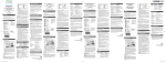
Steptep-byby -step guide “Get the Raspberry Pi up and running”
running”
•
•
•
•
•
•
26
get Linux running on the Raspberry Pi: detailed procedure on
http://elinux.org/RPi_Easy_SD_Card_Setup (in German)
get current Raspbian from http://www.raspberrypi.org/downloads
verify checksum and write image to SD card (ext4) – size of at least 4GB
recommended, the image alone needs about 2GB
o run sha1sum <file> on your zip file and compare to checksum from
download page
o unzip <file>
o insert SD card, get the card’s partition number (e.g. using df –h)
o unmount all SD partitions with umount /dev/<partition_number>
o write image to SD card
make sure to write the correct file behind ‘if=’
make sure to insert the whole SD card (not only one partition)
name for <SD_card> and make sure, you do not insert the
wrong device after ‘of=’ – all data on this device will be lost
4M should suffice, if not, try 1M
sudo dd bs=4M if=~/<unzipped_file> of=/dev/<SD_card>
dd command does not give any processing information, may seem
frozen, may take some minutes to finish – card reader should
blink while working
o run sudo sync to flush write cash – important to safely unmounts SD
card
insert SD card into Raspberry Pi, boot with screen adapted
first boot allows some configuration
o make sure to expand file system to be able to use the complete card
memory
o configure at your convenience
get MAC address to be able to register Raspberry Pi in the KIP network
o cat /sys/class/net/eth0/address
o register in KIP network (recommended host name: raspeval-xyz, where
xyz is the running number)
9 Addendum
•
•
•
•
prerequisites for I2C and 1-wire: compile kernel with required settings
o make sure, gcc compiler is installed on RPi (should be installed by
default)
o get kernel (on RPi) with git clone --depth 1
https://github.com/raspberrypi/linux.git
recommended: get kernel on desktop, then copy to SD card (or
use scp)
default folder: “linux” (this is your build directory)
in build directory: git checkout rpi-3.6.y
o make mrproper in build directory
o get .config file from current kernel via zcat /proc/config.gz > .config
o move the new .config to your build directory, if zcat was executed
elsewhere
o as root, edit .config to enable additional I2C
CONFIG_I2C_GPIO=m (compiled as module)
o 1-wire: supported in current kernel
change default pin from 4 to 14 (specified by ribbon cable layout)
as root, edit: <build_directory>/arch/arm/machbcm2708/bcm2708.c
• change #define W1_GPIO 4 to #define W1_GPIO 14
• change #define UART0_DMA { 15, 14 }
to #define UART0_DMA { 22, 25 } to avoid overwriting
pin 14, needed for 1-wire
o in build directory: make (lasts about six hours if compiled on Raspberry
Pi)
o as root in build directory:
make modules (lasts a few minutes on Raspberry Pi)
make modules_install (lasts a few minutes on Raspberry Pi)
o move the new kernel image from /arch/arm/boot/Image to /boot
(recommended: rename new image to e.g. kernel_new.img)
o in /boot: as root, edit config.txt
change kernel=kernel.img to kernel=kernel_new.img (or add this
line, if not existing)
test booting with new kernel, in case of success remove old kernel.img
enable I2C and 1-wire
native I2C: detailed procedure on http://www.gsurf.de/vorbereiten-desraspberry-pi-auf-i2c/ (German)
o as root, edit /etc/modprobe.d/raspi-blacklist.conf
make blacklist i2c-bcm2708 a comment
27
9 Addendum
•
•
28
o as root, edit /etc/modules, add the following lines:
i2c-bcm2708
ic2-dev
w1-gpio
w1-therm
additional I2C: add Kadamski I2C module to add/remove GPIO bit-banged I2C
busses
o get the module via git clone https://github.com/kadamski/i2c-gpioparam.git
o default (build) directory: i2c-gpio-param
o edit <build_directory>/i2c-gpio-param.c
busid = 2;
sda = 17; (use GPIO 17 as sda)
scl = 4;
(use GPIO 4 as scl)
udelay = 3; (use I2C speed of about 100 Hz)
timeout = 0;
sda_od = 0; //should switch sth. about open drain, with this one
scl_od = 0; //and the following enabled, not all devices are
//recognised => set to 0)
o for further explanations of parameters for the module see
https://github.com/kadamski/i2c-gpio-param
o attention: Because of another native I2C bus on another pin header, I2C
bus 0 of the clkboard programme will be I2C bus 1 on the RPi, I2C 1 of
the programme will be I2C bus 2 on the RPi
o as root, edit Makefile:
KDIR:=/home/pi/<build_directory>
o in build directory: make
o recommended: test module with modprobe and i2c-tools
o cp i2-gpio-param.ko /lib/modules/<version_number>/kernel/drivers/i2c
o add i2c-gpio-param to /etc/modules for autoload at boot (edit as root)
o using the kadamski module:
add bus via echo busid sda scl > /sys/class/i2c-gpio/add_bus
remove bus via echo busid > /sys/class/i2c-gpio/remove_bus
use GPIO numbers for sda and scl
further options on https://github.com/kadamski/i2c-gpio-param
after successful test, remove source files
9 Addendum
9.2 Setup for qemu compilation environment:
•
•
•
•
•
•
•
•
•
•
•
instructions from http://wiki.debian.org/QemuUserEmulation
download Raspbian image from Raspberry Pi homepage:
http://www.raspberrypi.org/downloads
(or use image used to set up Raspberry Pi in the beforehand)
resize image by dd if=/dev/zero bs=1M count=2048 >> file.img
grow filesystem by
losetup -f file.img
kpartx -a /dev/loop0
fsck /dev/mapper/loop0p2
resize2fs /dev/mapper/loop0p2
kpartx -d /dev/loop0
losetup -d /dev/loop0
mount file.img somewhere (offset from output of file file.img * 512, second
partition)
mount file.img -o loop,offset=62914560 /mnt/tmp
install on host: qemu qemu-user-static qemu-user-static
now, update-binfmts --display should include qemu stuff
copy /etc/resolv.conf to /mnt/tmp/etc/resolv.conf for DNS support
now, chroot /mnt/tmp should work
set proxy in chroot environment
export http_proxy=http://proxy.kip.uni-heidelberg.de
export https_proxy=https://proxy.kip.uni-heidelberg.de
in chroot, install, work, stuff...
•
•
•
to work on software:
sudo mount 2013...usw.usf..img -o loop,offset=62914560 /mnt/tmp
sudo chroot /mnt/tmp
•
•
•
•
•
•
•
•
•
29
9 Addendum
DI_VCCANA
VDDA
DI_VCC
VDD
VDD25
VDD5
VDD12
DI_VCC33ANA
VDDBUS
VOH
VOL
VBIAS
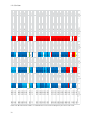
9.3 Measurement results
0 - 100 mA
1- 3A
> 0,4 A
1- 3A
all values
all values
not measured
only after FET
> 0 A; 0,2 - 0,5 A
> 50 mA
> 50 mA
all values
On these three pages the results of the communication
test between the Raspberry Pi and the clockboards are
presented. In the first table the optimum values and the
colour codes are listed.
almost always negative
most of the time/always too low
high fluctuation, often change of algebraic sign
diff - only one value measured, because of differential measurement
jumps between values
considerable fluctuations, mostly ca. ± half value till ± whole value
VDD25 and VBIAS given resistance value differs from value taken to calculate currnt
The second and third table contain the results with
corresponding colour-coding. It is obvious that
fluctuations occur voltage-dependent and not reticledependent. Some columns do not contain values, but
only the label “diff”. This indicates differential
measurement of the corresponding voltages. The voltage
VDD12, which occurs in the WSI documentation, is not
yet connected and thus not measured. For VCC33ANA
only the values after the FETs are measured. The values
before the FETs are given (3.3 V) for the current
calculation, which leads to negative current values
throughout the measurement.
The reticles which seem to be defective will be
investigated at a later stage.
To obtain the values every reticle was switched on
individually and the values were updated at least ten
times. As the measurements were not intended to deliver
precision values, no mean value was calculated, but a
value approximately in the middle of occurring
fluctuations was noted down.
Table 1: Optimal current values for different voltages and explanation of colour codes.
30
9 Addendum
PIC
1
2
3
4
5
6
7
8
9
10
11
12
13
14
15
16
17
18
19
20
21
22
23
24
Reticle
DI_VCCANA [V]
VDDA [V]
DI_VCC [V]
VDD [V]
VDD25 [V]
Current probe [I]
before FET after FET
current [I] before FET after FET
current [I] before FET after FET
current [I] before FET
after FET
current [I] before FET after FET
2
2,38
1,8062
1,8054
0,0180
1,8086
1,8034
1,5408
1,8106
1,8061
1,3293
1,8109
1,8057
1,5408
1,3761 diff
3
2,79
1,8053
1,8039
0,0360
1,8094
1,8033
1,7825
1,8099
1,8091
0,2115
1,8110
1,8027
2,4472
1,3496 diff
6
2,45
1,8068
1,8073
-0,0100
1,8087
1,8027
1,7513
1,8083
1,8077
0,1812
1,8102
1,8048
1,6003
1,3466 diff
45
2,32
1,8068
1,8058
0,0257
1,8091
1,8040
1,5097
1,8111
1,8100
0,3020
1,8101
1,8040
1,8117
1,6033 diff
1
2,32 all DI_voltages after FETs break down to almost 0 after few seconds
4
2,83
1,8088
1,8076
0,0308
1,8083
1,8055
0,8449
1,8123
1,8117
0,1811
1,8099
1,8056
1,2642
1,4594 diff
5
2,9
1,8074
1,8104
-0,0744
1,8073
1,8053
0,6035
1,8115
1,8150
-1,0260
1,8080
1,8062
0,5432
1,4950 diff
8
2,4
1,8080
1,8067
0,0333
1,8096
1,8062
0,9958
1,8118
1,8060
1,7201
1,8109
1,8092
0,5130
1,4887 diff
7
2,59
1,8080
1,8103
-0,0565
1,8093
1,8064
0,8459
1,8108
1,8127
-0,5740
1,8102
1,8070
0,9366
1,4553 diff
12
2,5
1,8083
1,8071
0,0308
1,8098
1,8068
0,8761
1,8106
1,8089
0,4834
1,8107
1,8075
0,9366
1,4682 diff
11
2,39
1,8109
1,8101
0,0206
1,8133
1,8059
2,1766
1,8133
1,8124
0,2721
1,8133
1,8074
1,7231
2,3759 diff
46
2,33
1,8107
1,8095
0,0308
1,8113
1,8050
1,8441
1,8114
1,8087
0,7860
1,8144
1,8077
1,9952
2,3754 diff
1,8138
1,8105
0,9757
1,5094 diff
9
2,3
1,8113
1,8113 always 0
1,8138
1,8080
1,7075
1,8113
1,8105 0 or 0,243923
10
2,3
1,8146
1,8113
0,0829
1,8171
1,8080
2,6832
1,8154
1,8113
1,2196
1,8146
1,8105
1,2196
1,4986 diff
14
2,33
1,8095
1,8094 ±0,00258684
1,8109
1,8048
1,7953
1,8124
1,8102
0,6694
1,8117
1,8069
1,3997
1,5278 diff
15
2,31
1,8102
1,8090
0,0284
1,8097
1,8049
1,4301
1,8123
1,8115
0,2434
1,8104
1,8061
1,2476
1,4016 diff
16
2,33
1,8112
1,8106
0,0156
1,8121
1,8074
1,3733
1,8137
1,8112
0,7324
8,8126
1,8086
1,1597
1,5072 diff
13
2,38
1,8125
1,8110
0,0363
1,8127
1,8065
1,8311
1,8154
1,8108
1,3428
1,8148
1,8086
1,8005
1,4880 diff
18
2,58
1,8120
1,8124
-0,0104
1,8135
1,8083
1,5259
1,8159
1,8170
-0,3357
1,8132
1,8088
1,2817
1,5706 diff
17
2,3 all DI_voltages after FETs break down to almost 0 after few seconds
20
2,31
1,8148
1,8131
0,0415
1,8140
1,8074
1,9204
1,8125
1,8099
0,7620
1,8156
1,8099
1,6765
1,4311 diff
23
2,35
1,8157
1,8146
0,0258
1,8130
1,8069
1,7984
1,8174
1,8168
0,1829
1,8144
1,8092
1,5241
1,4664 diff
19
3,02
1,8120
1,8137
-0,0440
1,8115
1,8080
1,0354
1,8135
1,8154
-0,5482
1,8109
1,8055
1,5837
1,5702 diff
24
2,24
1,8120
1,8110
0,0233
1,8109
1,8080
0,8508
1,8103
1,8090
0,3959
1,8112
1,8098
0,4264
1,5253 diff
22
2,36
1,8111
1,8134
-0,0566
7,8097
1,8073
0,6957
1,8120
1,8149
-0,8469
1,8125
1,8097
0,8469
1,5066 diff
34
2,53
1,8097
1,8086
0,0257
1,8099
1,8047
1,5124
1,8109
1,8098
0,3327
1,8118
1,8079
1,1495
0,8847 diff
25
2,64
1,8120
1,8106
0,0339
1,8127
1,8049
2,2975
1,8130
1,8114
0,4837
1,8127
1,8062
1,9045
1,4219 diff
26
2,59
1,8113
1,8095
0,0437
1,8129
1,8050
2,3277
1,8138
1,8132
0,1814
1,8126
1,8063
1,8440
2,5238 diff
21
2,25
1,8112
1,8097
0,0385
1,8126
1,8059
1,9644
1,8108
1,8090
0,5440
1,8131
1,8086
1,3297
1,5485 diff
28
2,4
1,8126
1,8116
0,0231
1,8130
1,8063
1,9644
1,8150
1,8147
0,0907
1,8137
1,8077
1,7528
1,5269 diff
30
1,3 enabling FETs switches off half of the voltages, VDD25 at ca. 3,3 V
29 ca. 0
almost no voltage behind FETs
27
2,27
1,8106
1,8105
0,0026
1,8117
1,8071
1,3567
1,8104
1,8106
-0,0604
1,8119
1,8093
0,7858
1,4458 diff
31
2,5
1,8112
1,8102
0,0257
1,8112
1,8071
1,2089
1,8141
1,8134
0,2116
1,8116
1,8078
1,1182
1,5124 diff
1,8082
0,967348 1,8073 springt zw. 0 und
1,8090
1,8073
0,4837
1,9299 diff
32
2,46
1,8082
1,8090
-0,0206
1,8090
1,8049 springt zw. 1,2093 u.
35
2,46 0 V before FETs and some values behind FETs, for VBIAS, VDD5, VDD12 and VDD25 vice versa
36
2,38
1,8060
1,8059 >0: 0,00258386
1,8059
1,8016
1,2468
1,8056
1,8043
0,3649
1,8067
1,8036
0,9123
1,4145 diff
33
2,52
1,8075
1,8068
0,0181
1,8072
1,8015
1,6725
1,8091
1,8084
0,2129
1,8078
1,8030
1,4293
1,5057 diff
38
2,5
1,8087
1,8083 >0: 0,0103444
1,8084
1,8021
1,8561
1,8085
1,8094
-0,2738
1,8090
1,8048
1,2476
1,8828 diff
39
2,52
1,8087
1,8077
0,0259
1,8070
1,8018
1,5518
1,8086
1,8080
0,1826
1,8084
1,8038
1,3388
1,2633 diff
u. neg. Vielfachen
1,7968 von 0,0129312
1,7952
1,8096
1,8100
-0,1217
1,8052
1,8022
0,8824
1,4563 diff
40
2,96
1,8067
1,8066 springt zw. 0 u. pos.1,8029
37
2,44
1,8054
1,8043
0,0262
1,8055
1,7999
1,6431
1,8055
1,8049
0,1826
1,8071
1,8026
1,3388
1,9382 diff
47
2,49
1,8075
1,8078
-0,0078
1,8073
1,8020
1,5518
1,8077
1,8082
-0,1521
1,8087
1,8040
1,3693
1,3861 diff
44
2,43 all DI_voltages after FETs break down to almost 0 after few seconds
42
2,39
1,8084
1,8095
-0,0284
1,8086
1,8042
1,2776
1,8086
1,8108
-0,6388
1,8098
1,8069
0,8517
1,5394 diff
41
2,63
1,8091
1,8081
0,0257
1,8071
1,8035
1,0627
1,8098
1,8080
0,5475
1,8091
1,8047
1,3080
1,4887 diff
43
2,66
1,8082
1,8089
-0,0181
1,8086
1,8028
1,7020
1,8093
1,8103
-0,3039
1,8090
1,8044
1,3676
1,5048 diff
48
2,44
1,8078
1,8061
0,0439
7,8096
1,8035
1,7931
1,8043
1,8019
0,6990
1,8097
1,8059
1,0941
1,5141 diff
current [I]
0,6880
0,6748
0,6733
0,8016
0,7297
0,7475
0,7444
0,7276
0,7341
1,1880
1,1877
0,7547
0,7493
0,7639
0,7008
0,7536
0,7440
0,7853
0,7156
0,7332
0,7851
0,7627
0,7533
0,4423
0,7110
1,2619
0,7742
0,7635
0,7229
0,7562
0,9649
0,7073
0,7529
0,9414
0,6316
0,7282
0,9691
0,6930
0,7697
0,7443
0,7524
0,7571
Table 2.1: Measurement results of communication test between Raspberry Pi and clockboards.
31
9 Addendum
VDD5 [V]
before FET after FET
0,6078 diff
0,6067 diff
0,6032 diff
0,6028 diff
-0,0952
-0,4086
-82,5144
1,2364
1,2369
1,2342
0,7044
-0,0258
0,7038
-0,0362
0,7061
-0,0259
0,7066
0,0233
0,7000
-0,0698
0,7047 <0: -0,0362098
0,7072
-0,2026
1,4605 diff
0,6016 diff
0,6000 diff
0,5984 diff
0,5974 diff
1,0001 diff
1,0011 diff
0,6038 diff
0,6038 diff
0,6008 diff
0,6006 diff
0,6024 diff
0,6026 diff
0,6026 diff
0,1068
0,1066
0,1064
0,1064
0,1069
0,0962
0,1065
0,1061
0,1066
0,1067
3,3038
3,3163
3,3006
0,7034
0,7024
0,7050
0,7075
0,6972
0,7033
0,7062
current [I]
0,2676
0,2675
0,2664
0,2661
0,2676
0,2669
0,2664
0,2642
0,2638
0,5038
0,4988
0,2670
0,2670
0,2658
0,2657
0,2658
0,2657
0,2660
0,2737
0,2732
0,2722
0,2721
0,2703
0,2674
0,2715
0,2712
0,2725
0,2722
32
DI_VCC33ANA [V]
VDDBUS [V]
VOH [V]
VOL [V]
VBIAS [V]
current [I] before FET after FET
current [I] before FET after FET
current [I] before FET after FET
current [I] before FET after FET
current [I] before FET after FET
0,1057
3,3000
3,3126
-0,2735
1,2362
1,2351
0,3021
0,7116
0,7118
-0,0231
0,9067
0,9035
0,0796
0,5353 diff
0,1055
3,3000
3,3107
-0,2710
1,2358
1,2352
0,1511
0,7127
0,7131
-0,0154
0,9042
0,9028
0,0591
0,5350 diff
0,1049
3,3000
3,3023
0,0575
1,2346
1,2363
-0,4831
0,7064
0,7086
-0,0539
0,9049
0,9025
0,0590
0,5327 diff
0,1048
3,3000
3,3116
-0,2911
1,2353
1,2364
-0,3020
0,7028
0,7024
0,0103
0,9040
0,9025
0,0385
0,5322 diff
3,3000
0,1051
3,3000
3,3119
-0,2983
1,2517
1,2540
-0,6639
0,7055
0,7088
-0,0821
0,9065
0,9048
0,0410
0,5352 diff
0,1046
3,3000
3,3167
-0,4163
1,2362
1,2395
-0,9656
0,7068
0,7109
-0,1026
0,9039
0,9070
-0,0769
0,5338 diff
0,1043
3,3000
3,3051
-0,1264
1,2356
1,2392
-1,0562
0,7064
0,7080
-0,0410
0,9068
0,9064
0,0103
0,5327 diff
0,1041
3,3000
3,3123
-0,3069
1,2353
1,2348
-0,6345
0,0704
0,7100
-0,0745
0,9055
0,9053
0,0051
0,5283 diff
0,1039
3,3000
3,3069
-0,1734
1,2356
1,2380
-0,6949
0,7064
0,7061
0,0077
0,9032
0,9040
-0,0180
0,5277 diff
0,1739
3,3000
3,3105
-0,2636
1,2379
1,2375
0,1209
0,7094
0,7085
0,0231
0,9059
0,9037
0,0565
1,0076 diff
0,1741
3,3000
3,3051
-0,1274
1,2377
1,2376
0,0302
0,7083
0,7082
0,0026
0,9062
0,9030
0,0822
0,9976 diff
0,1050
3,3000
3,3099
-0,2480
1,2374
1,2374 0 or 0,243923 or 0,487846
0,7099
0,7091 0 or discrete positive
0,9056
or negative0,9023
value
0,0829
0,5341 diff
0,1050
3,3000
3,3124
-0,3102
1,2407
1,2374
0,9757
0,7066
0,7099
-0,0829
0,9098
0,9023
0,1866
0,5341 diff
0,1045
3,3000
3,3079
-0,1964
1,2363
1,2366
-0,0913
0,7093
0,7111
-0,0466
0,9068
0,9054
0,0336
0,5317 diff
0,1044
3,3000
3,3093
-0,2326
1,2372
1,2371
0,0304
0,7094
0,7097
-0,0078
0,9049
0,9041
0,0207
0,5313 diff
0,1048
3,3000
3,3089
-0,2225
1,2370
1,2372
-0,0610
0,7085
0,7101
-0,0415
0,9046
0,9034
0,0285
0,5317 diff
0,1048
3,3000
3,3119
-0,2977
1,2374
1,2378
-0,0915
0,7100
0,7103
-0,0078
0,9064
0,9050
0,0363
0,5314 diff
0,5321 diff
0,1048
3,3000
3,3180
-0,4507
1,2374
1,2385
-0,3052
0,7069
0,7115
-0,1141
0,9061
0,9051 >0: 0,0259399
3,3000
3,3000
3,3076
-0,1899
1,2470
1,2458
0,3353
0,7091
0,7086
0,0130
0,9078
0,9042
0,0881
0,5473 diff
3,3000
3,3200
-0,5008
1,2480
1,2462 >0: 0,51821
0,7098
0,7085 >0: 0,0336826
0,9073
0,9038
0,0881
0,5465 diff
3,3000
3,3164
-0,4042
1,2436
1,2459
-0,6700
0,7072
0,7106
-0,0854
0,9043
0,9041
0,0052
0,5443 diff
3,3000
3,3099
-0,2463
1,2441
1,2468
-0,7918
0,7062
0,7065
-0,0078
0,9064
0,9022
0,1061
0,5442 diff
3,3000
3,3155
-0,3873
1,2438
1,2466
-0,8167
0,7060
0,7087
-0,0668
0,9019
0,9029
-0,0231
0,5407 diff
3,3000
3,3110
-0,2742
1,2717
1,2434
-0,4840
0,7050
0,7053
-0,0077
0,9005
0,9029
-0,0594
0,5348 diff
3,3000
3,3129
-0,3227
1,2480
1,2477
0,0907
0,7064
0,7077
-0,0308
0,9055
0,9028 >0: 0,0668094
0,5429 diff
3,3000
3,3150
-0,3741
1,2485
1,2481
0,1209
0,7074
0,7069
0,0103
0,9057
0,9019
0,0951
0,5425 diff
3,3000
3,3057
-0,1414
1,2361
1,2365
-0,1209
0,7078
0,7069
0,0206
0,9055
0,9018
0,0925
0,5450 diff
0,7091
-0,0283
0,9063
0,9042 >0: 0,0513762
0,5444 diff
3,3000
3,3163
-0,4086
1,2375
1,2361 zw. 0,4 und -0,4 0,7080
0,6144 diff
0,6127 diff
0,6115 diff
0,6119 diff
0,6146 diff
0,5529 diff
0,6124 diff
0,6102 diff
0,6132 diff
0,6134 diff
3,3000
3,3000
0,0000
0,0608
-0,2433
0,3347
0,2130
0,1217
-0,2130
-0,0609
0,2717
0,2717
0,2738
0,1066
0,1066
0,1067
1,2335
1,2341
1,2339
1,2345
1,2463
1,2470
1,2361
1,2373 <0: -0,241749
0,7059
0,7096 <0: -0,0924766
0,9072
0,9046
0,0642
0,5434 diff
1,2381
-0,3325
0,7056
0,7021
0,0873
0,9062
0,9025
0,0925
0,5434 diff
u. -0,4837090,7071
u. -0,725529
springt zw. -0,0206 0,9037
u. -0,0411 u. -0,0617
0,9020 springt
u. -0,0822
zw. 0,0411 u.
0,5476
0,0822diff
1,2350 springt zw. -0,241820,7039
0,6130 diff
0,6131 diff
0,6134 diff
1,2335
1,2333
1,2350
1,2353
1,2467
1,2463
1,2359
-0,0621
-0,0414
-0,0258
0,2325
0,2704
0,2705
0,2707
0,2706
0,2698
0,2693
0,2694
0,0126
-0,3596
-0,3128
-0,2740
-0,1344
-0,1861
-0,1887
0,7074
0,7062
0,7100
0,7022
0,5408 diff
0,5410 diff
0,5415 diff
0,5413 diff
0,5396 diff
0,5387 diff
0,5388 diff
3,2995
3,3144
3,3125
3,3110
3,3054
3,3074
3,3076
0,7049
0,7045
0,7090
0,7032
0,0853
0,0569
0,0414
0,0414
0,1500
0,0621
0,0103
3,3000
3,3000
3,3000
3,3000
3,3000
3,3000
3,3000
-0,4563
-0,5780
-0,3647
-0,3647
0,8991
0,9014
0,9037
0,9031
0,8965
0,9008
0,9044
0,1059
0,1060
0,1057
0,1057
0,1056
0,1053
0,1059
1,2378
1,2375
1,2359
1,2361
0,9025
0,9037
0,9053
0,9047
0,9025
0,9033
0,9048
0,6088 diff
0,6096 diff
0,6075 diff
0,6075 diff
0,6074 diff
0,6057 diff
0,6091 diff
1,2362
1,2355
1,2346
1,2348
0,2685
0,2685
0,2703
0,2701
-0,3711
-0,3323
-0,3753
-0,0627
0,5370 diff
0,5370 diff
0,5406 diff
0,5401 diff
3,3148
3,3133
3,3150
3,3025
0,0284
-0,0103
-0,0284
0,0517
3,3000
3,3000
3,3000
3,3000
0,9042
0,9054
0,9039
0,9007
0,1056
0,1056
0,1060
0,1058
0,9054
0,9050
0,9027
0,9028
0,6073 diff
0,6070 diff
0,6092 diff
0,6084 diff
Table 2.2: Measurement results of communication test between Raspberry Pi and clockboards.
Statement of Originality (Erklärung
(Erklärung):
Erklärung ):
I certify that this thesis and the research to which it refers are the product of my own work.
Any ideas or quotations from the work of other people published or otherwise, are fully
acknowledged in accordance with the standard referencing practices of the discipline.
Ich versichere, dass ich diese Arbeit selbständig verfasst und keine anderen als die angegebenen
Quellen und Hilfsmittel verwendet habe.
Markus Hellenbrand
Heidelberg, 12 July 2013