1
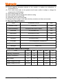
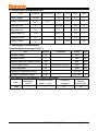
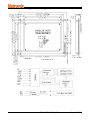
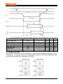
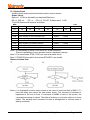
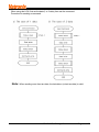
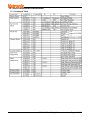
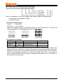
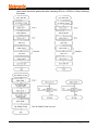
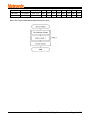
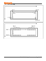
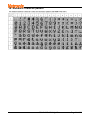
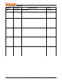
LCD Module User Manual
Customer
:
MASS PRODUCTION CODE : TG160128B-03WA0
DRAWING NO.
: M-TG160128B-03WA0_A00
Approved By Customer:
Date:
Approved By
Checked By
Prepared By
Vatronix Holdings Limited
ADD:5F,No.10 Blg,WenGuang Industrial Zone,XiLi,Nanshan District,Shenzhen,China
TEL:0086-755-83234801 33207538
E-mail:[email protected]
FAX:0086-755-33207539
Http://www.vatronix.com
TG160128B-03WA0_A00
Page 1 of 27
Contents
1. Precautions in Use of LCD Module------------------------------------P3
2. General Specification-------------------------------------------------------P3
3. Absolute Maximum Ratings-----------------------------------------------P3
4. Electrical Characteristics--------------------------------------------------P4
5. Backlight Information-------------------------------------------------------P4
6. Optical Characteristics-----------------------------------------------------P5
7. Interface Description--------------------------------------------------------P6
8. Contour Drawing & Block Diagram--------------------------------------P7
9. Application circuit----------------------------------------------------------P8
10. Timing Characteristics -----------------------------------------------P9
11 .RAM Interface ----------------------------------------------P 9
12. Flowchart of communications with MPU ---------------------------P10
13. User instruction Definitions -------------------------------------------P12
14. Initializing flow chart ---------------------------------------------------P24
15. LCM RAM map -----------------------------------------------------------P25
16. Standard Character pattern -------------------------------------------P26
17. Revision records------------------------------------------------------P27
TG160128B-03WA0_A00
Page 2 of 27
1. Precautions in Use of LCD Module
(1) Avoid applying excessive shocks to the module or making any alterations or
modifications to it.
(2) Don’t make extra holes on the printed circuit board, modify its shape or change the
components of LCD Module.
(3) Don’tdisassemble the LCM.
(4) Don’toperate it above the absolute maximum rating.
(5) Don’tdrop, bend or twist LCM.
(6) Soldering: only to the I/O terminals.
(7) Storage: please storage in anti-static electricity container and clean environment.
2. General Specification
ITEM
STANDARD VALUE
UNIT
Number of dots
160X128
Dots
Outline dimension
129.0(W)X104.5(H)X12.0MAX.
mm
View area
101.0(W)X82.0(H)
mm
Active area
95.96(W)X76.76(H)
mm
Dot size
0.56(W)X0.56(H)
mm
Dot pitch
0.60(W)X0.60(H)
mm
LCD type
STN,Grey,positive, transflective
View direction
6 o’clock
Backlight
White LED
3. Absolute Maximum Ratings
ITEM
SYMBOL
MIN.
Operating Temperature
TOP
0
Storage Temperature
TST
MAX.
UNIT
-
+60
℃
-10
-
+70
℃
VI
-0.3
-
VDD +0.3
V
Supply Voltage For Logic
VDD
0
-
5.5
V
Supply Voltage For LCD
VDD-VEE
0
-
20.0
V
Input Voltage
TYPE
TG160128B-03WA0_A00
Page 3 of 27
4. Electrical Characteristics
ITEM
SYMBOL
Logic Voltage
VDD-VSS
Supply Volt.For LCD
VDD-VO
CONDITION
Ta=25℃
MIN.
TYPE
MAX.
UNIT
4.5
5.0
5.5
V
---
13.5
---
V
Input High Volt.
VIH
-
VDD -2.2
-
VDD
V
Input Low Volt.
VIL
-
0
-
0.8
V
Output High Volt.
VOH
-
VDD –0.3
-
VDD
V
Output Low Volt.
VOL
-
0
-
0.3
V
Supply Current
IDD
-
---
---
mA
18.0
5. Backlight Information
Absolute Maximum ratings (Ta=25℃)
Item
Symbol
Conditions
Rating
Unit
Reverse voltage
Vr
-
10.0
V
Reverse Current
Ir
-
400
uA
800
mA
2400
mA
Absolute maximum forward Current
Ifm
Peak forward current
Ifp
Power dissipation
Pd
4000
mW
Toper
-30~+70
℃
Tst
-40~+80
℃
Operating Temperature Range
Storage Temperature Range
I msec plus 10% Duty Cycle
Electrical/Optical Characteristics (Ta=250C,If=110mA)
Color
White
λp(nm)
Spectral line half
widthΔλ(nm)
---
---
Wavelength
Operating
voltage(v)
3.0
TG160128B-03WA0_A00
Forward
Current (mA)
110
Page 4 of 27
6. Optical Characteristics
ITEM
SYMBOL CONDITION
MIN
TYPE
MAX
UNIT
(V)θ
CR≧2
10
-
120
deg.
(H)φ
CR≧2
-45
-
45
deg.
Contrast Ratio
CR
-
-
5
-
-
Response Time
T rise
-
-
200
300
ms
T fall
-
-
150
200
ms
View Angle
TG160128B-03WA0_A00
Page 5 of 27
7.Interface Description
Pin No.
Symbol
Level
Description
1
FG
---
Frame ground
2
VSS
0V
Ground
3
VDD
5.0V
4
VO
5
/WR
L
Write signal,active LOW
6
/RD
L
Read signal,active LOW
7
/CE
L
Chip enable,active LOW
8
C/D
H/L
H :Command L:Data
9
NC
---
No connectiion
10
/RST
L
LCM reset,active LOW
11~18
DB0~DB7
H/L
19
20
FS
VEE
H/L
-15V
21
A(LED+)
+5V
22
K(LED-)
0V
Power supply for Logic
(Variable) Driving voltage for LCD
8-bit Data bus
Font select H:6x8 L:8x8 (Default: “L”)
Negative voltage output (Default:No connection)
(Option:built-in DC-DC convertor)
Anode of LED Backlight
Note1
Cathode of LED Backlight Note1
Note1:PIN21,PIN22 floating when Backlight power supply slectection jumper JA,JK shorted
TG160128B-03WA0_A00
Page 6 of 27
8. Contour Drawing & Block Diagram
TG160128B-03WA0_A00
Page 7 of 27
9. Application circuit
9.1 Interfaces with 8080-series MPU
The LCM can be directly connected to an 8080-series MPU. The LCM can be used with
an 8080-serial MPU as shown in the following application circuit.
9.2 Interfaces with 6800-series MPU
TG160128B-03WA0_A00
Page 8 of 27
10. Timing Characteristics
Test Conditions (Unless Otherwise Noted, VDD = 5.0 V ± 10%, VSS = 0 V, Ta = -20~75°C)
Item
C / D Set-up Time
C / D Hold Time
/CE,/RD,/WR pulse width
Data Set-up Time
Data Hold Time
Access Time
Output Hold Time
Symbol
Test conditions
MIN.
MAX.
Unit
tCDS
tCDH
tCE, tRD, tWR
-------
100
10
80
------
ns
ns
ns
tDS
tDH
tACC
tOH
---------
80
40
--10
----150
50
ns
ns
ns
ns
11. RAM Interface
This LCM use dual-scan mode, the address of upper LCD is allocated to 0000H to 7FFFH
(32KB MAX.), the address of lower LCD is allocated to 8000H to FFFFH(32 KB MAX).Detail
specification see page 8th in data sheet of T6963C.
TG160128B-03WA0_A00
Page 9 of 27
12.Flowchart of communications with MPU
12.1 Status Read
A status check must be performed before data is read or written.
Status Check
Status of LCM can be read from data lines(Data bus).
RD = L, WR = H,
CE = L, C/D = H, D0~D7 àStatus word LCM.
The LCM Status word format is as follows.
MSB
LSB
STA7
STA6
STA5
STA4
STA3
STA2
STA1
STA0
D7
D6
D5
D4
D3
D2
D1
D0
STA0
check capability of command execution
0: disable
1:enable
STA1
check capability of data read/write
0: disable
1:enable
STA2
check capability of auto mode data read
0: disable
1:enable
STA3
check capability of auto mode data write
0: disable
1:enable
STA4
not use
STA5
check capability of controller operation
0: disable
1:enable
STA6
error flag. using screen peek/copy command
0: no error
STA7
check the condition blink
0: display off 1:normal display
Note1: It is necessary to check STA0 and STA1 at the same time.
There is a possibility of error operation due to a hardware interrupt.
Note 2. For most modes STA0 / STA1 are used as a status check.
Note 3. STA2/STA3 are valid in Auto mode;STA0/STA1 are invalid.
Status checking flow
Note 4. It is impossible to save status check in the case of command that is MSB 0. To
have the delay time cannot be save status check. The interrupt of hardware is
happened at the end of lines. If command of MSB0 is sent in this period, the
command executing is waited. The state of waiting is not known without to check
status. The sending next command or data is disregarded or rewrites data of
waiting command.
TG160128B-03WA0_A00
Page 10 of 27
12.2 Data Set
When using the LCM, first set the data(1 or 2 data), then set the command.
Procedure for sending a command
Note: When sending more than two data, the last datum (or last two data) is valid.
TG160128B-03WA0_A00
Page 11 of 27
13. User instruction Definitions
13.1 Command Table
TG160128B-03WA0_A00
Page 12 of 27
13.2 Description of command
13.2.1 Register setting
CODE
HEX
FUNCTION
00100001
21H
CURSOR POINTER SET
X address
Y address
00100010
00100100
22H
24H
OFFSET REGISTER SET
ADDRESS POINTER SET
DATA(DB0~DB4 is valid)
LOW address
00H
HIGH address
D1
D2
(1) CURSOR POINTER SET ( D1-D2-21H )
The position of cursor is specified by X address, Y address, The cursor position is
moved only by this command. The cursor pointer doesn‘t have the function of
increment and decrement. The shift of cursor are set by this command.
X address, Y address are specified following
X address
00H~4FH (lower 7bits are valid)
Y address
00H~1FH (lower 5bits are valid)
1) 1 screen drive
2) 2 screen drive
X ADRS 00~4FH
X ADRS 00~4FH
Y ADRS 0H~0FH
upper screen
Y ADRS 00H~0FH
YADRS 10H~1FH
lower screen
(2)OFFSET REGISTER SET( D1-00-22H )
The offset register is used to determine external Character Generator RAM area.
The LCM assign External character generator, when character code set 80H to FFH in
using internal character generator. Character code 00H to 80H assign External
Character Generator, when External generator mode.
The senior five bits define the start address in external memory of the CG RAM area.
The next eight bits represent the character code of the character. In internal CG ROM
mode, character codes 00H to 7FH represent the predefined “internal”CG ROM
characters, and codes 80H to FFH represent the user’s own “external”characters. In
external CG RAM mode, all 256 codes from 00H to FFH can be used to represent the
user' s own characters. The three least significant bits indicate one of the eight rows of
eight dots that define the character’s shape.
MSB
AD15
AD14
LSB
AD13
AD12
AD11
Offset Register Data(5-bit)
AD10
AD9
AD8
AD7
AD6
AD5
AD4
AD3
Character Code(8-bit)
AD2
AD1
AD0
Line Scan(3-bit)
The relationship between display RAM address and offset register
Offset register data
CG RAM hex. address (start to end)
00000
0000 to 07FFH
00001
0800 to 0FFFH
00010
1000 to 17FFH
11100
E000 to E7FFH
11101
E800 to EFFFH
11110
F000 to F7FFH
11111
F800 to FFFFH
TG160128B-03WA0_A00
Page 13 of 27
(Example 1)
Offset register 02H
Character code 80H
Character generator RAM start address:1400H
MSB
AD15
0
LSB
AD14
0
AD13
0
AD12
1
AD11
0
AD10
AD9
AD8
AD7
1
0
0
0
AD6
0
AD5
AD4
AD3
0
0
0
AD2
0
AD1
0
AD0
0
Character generator RAM start address: 1400H
(3) Set Address Pointer(D1-D2-24H)
The address point set command is used to indicate the start address for writing to ( or
reading from) external RAM.
13.2.2 Control word set
CODE
HEX
FUNCTION
01000000
40H
TEXT HOME ADDRESS SET
Low address
High address
01000001
41H
TEXT AREA SET
Columns
00H
01000010
42H
GRAPHIC HOME ADDRESS SET
Low address
High address
01000011
43H
GRAPHIC AREA SET
Columns
00H
D1
D2
The home address and column size are defined by this command.
(1) Text home address set( D1-D2-40H )
The starting address of external display RAM for Text display is defined by this
command. The text home address shows the left end and most upper position.
The relationship of external display RAM address and display position
TH
TH + CL
TH + TA
TH + TA + CL
(TH + TA) + TA
TH + 2TA + CL
(TH + 2TA) + TA
TH + 3TA + CL
~
~
TH + (n-1) TA
TH + (n-1) TA + CL
TH: Text Home address TA: Text Area number (columns)
CL: Columns are fixed by hardware, pin-programmable,this LCM can be set by
jumper”J3” ,When J3 connected to “V” ,CL=32,and connected to “G”, CL=40.
Default: CL=40.
(example) Text home address = 0000H
Text area = 0020H
CL=32 columns
4 lines
TG160128B-03WA0_A00
Page 14 of 27
0000H
0001H
001EH
001FH
0020H
0021H
003EH
003FH
0040H
0041H
005EH
005FH
0060H
0061H
007EH
007FH
(2) Graphic home address set (D1-D2-42H)
The starting address of external display RAM for Graphic display is defined by this
command.
The graphic home address shows the left end and most upper line.
The relationship of external display RAM address and display position
GH
GH+CL
GH+GA
CH+GA+CL
(GH+GA)+GA
GH+2GA+CL
(GH+2GA)+GA
GH+3GA+CL
~
~
GH+(n-1)GA
GH+(n-1)GA+CL
GH: Graphic Home address
GA:Graphic area number (columns)
CL: Columns are fixed by hardware, pin-programmable,this LCM can be set by
jumper”J3”,When J3 connected to “V”,CL=32,and connected to “G”,CL=40.
Default: CL=40.
(example) Graphic home address = 0000H
Graphic area = 0020H
CL=32 columns
2 lines
0000H
0001H
001EH
001FH
0020H
0021H
003EH
003FH
0040H
0041H
005EH
005FH
0060H
0061H
007EH
007FH
0080H
0081H
009EH
009FH
00A0H
00A1H
00BEH
00BFH
00C0H
00C1H
00DEH
00DFH
00E0H
00E1H
00FEH
00FFH
0100H
0101H
011EH
011FH
0120H
0121H
013EH
013FH
0140H
0141H
015EH
015FH
0160H
0161H
017EH
017FH
01A0H
01A1H
01BEH
01BFH
01C0H
01C1H
01DEH
01DFH
01E0H
01E1H
01FEH
01FFH
(3)Text area set(D1-00-41H)
The columns of display are defined by the hardware setting. This command can be
used to adjust columns of display.
TG160128B-03WA0_A00
Page 15 of 27
(example) LCD size: 20 columns, 4 lines
Text home address = 0000H
CL=32 columns
0000
0014
0028
003C
.
.
.
.
.
.
.
.
.
.
.
.
.
.
.
.
.
.
.
.
.
.
.
.
.
.
.
.
0001
0015
0029
003D
Text area = 0014H
4 lines
0013
0027
003B
004F
0014
0028
003C
0050
.
.
.
.
.
.
.
.
.
.
.
.
.
.
.
.
.
.
.
.
001F
0033
0047
005B
LCD
(4) Graphic area set (D1-00-43H)
The columns of display are defined by the hardware setting. This command can be
used to adjust columns of graphic display.
(example)
LCD size: 20 columns, 2 lines
Graphic home address= 0000H Graphic area = 0014H
CL=32 columns
2 lines
0000
0014
0028
003C
0050
0064
0078
008C
00A0
00B4
00C8
00DC
00F0
0104
0128
013C
0001
0015
0029
003D
0051
0065
0079
008D
00A1
00B5
00C9
00DD
00F1
0105
0129
013D
.
.
.
.
.
.
.
.
.
.
.
.
.
.
.
.
.
.
.
.
.
.
.
.
.
.
.
.
.
.
.
.
.
.
.
.
.
.
.
.
.
.
.
.
.
.
.
.
.
.
.
.
.
.
.
.
.
.
.
.
.
.
.
.
.
.
.
.
.
.
.
.
.
.
.
.
.
.
.
.
.
.
.
.
.
.
.
.
.
.
.
.
.
.
.
.
.
.
.
.
.
.
.
.
.
.
.
.
.
.
.
.
0013
0027
003B
004F
0063
0077
008B
009F
00B3
00C7
00DB
00EF
0103
0127
013B
014F
0014
0028
003C
0050
0064
0078
008C
00A0
00B4
00C8
00DC
00F0
0104
0128
012C
0140
.
.
.
.
.
.
.
.
.
.
.
.
.
.
.
.
.
.
.
.
.
.
.
.
.
.
.
.
.
.
.
.
.
.
.
.
.
.
.
.
.
.
.
.
.
.
.
.
.
.
.
.
.
.
.
.
.
.
.
.
.
.
.
.
.
.
.
.
.
.
.
.
.
.
.
.
.
.
.
.
001F
0033
0047
005B
006F
0083
0097
00AB
00BF
00D3
00E7
00FD
011F
0123
0137
014B
LCD
The address in graphic area can be continuous and RAM area can be used without
ineffective area, if graphic area is defined the same number as the actual column
number of LCD display.
13.2.3 Mode set
CODE
FUNCTION
Operand
1000X000
“OR”mode
1000X001
“EXOR”mode
1000X011
“AND”mode
1000X100
“TEXT ATTRIBUTE”mode
10000XXX
internal character generator mode
10001XXX
external character generator mode
X:invalid
The display mode is defined by this command. The display mode doesn‘t change until
this command is sent. Logically “OR”, “EXOR”, “AND”of text and graphic display can be
displayed. When internal character generator mode is selected, character code 00H~7FH
are selected from built-in character generator RM. The character code 80H~FFH are
automatically selected from external character generator RAM.
TG160128B-03WA0_A00
Page 16 of 27
(example)
■■■■■■■■
■■■■■■■■
■■■■■■■■
■■■■■■■■
■■■■■■■■
■■■■■■■■
■■■■■■■■
■■■■■■■■
□□□□□□□□
□□□■■■■■
□□□□□■□□
□□□□□■□□
□□□□□■□□
□□□□□■□□
□□□□□■□□
□□□□□□□□
Graphic
Text
■■■■■■■■
■■■■■■■■
■■■■■■■■
■■■■■■■■
■■■■■■■■
■■■■■■■■
■■■■■■■■
■■■■■■■■
□□□□□□□□
□□□■■■■■
□□□□□■□□
□□□□□■□□
□□□□□■□□
□□□□□■□□
□□□□□■□□
□□□□□□□□
“OR”
■■■■■■■■
■■■□□□□□
■■■■■□■■
■■■■■□■■
■■■■■□■■
■■■■■□■■
■■■■■□■■
■■■■■■■■
“AND”
“EXOR”
Only text display is attributed, because attribute data is located in graphic RAM
area.
Note:
Attribute function
“Reverse display”, “Character blink”and “Inhibit”are called “Attribute”. The attribute data
is written into the graphic area defined by “Control word set”command. Only text display
is possible in Attribute Function mode; graphic display is automatically disabled. However,
the Display Mode command must be used to turn both Text and Graphic on in order for
the Attribute function to be available.
The attribute data of the 1st character in text area is written at the 1st 1 byte in graphic
area, and attribute data of n-th character is written at the n-th 1 byte in graphic area.
Attribute function is defined as follows:
Attribute RAM 1 Byte
d3
0
0
0
1
1
1
d2
0
1
0
0
1
0
d1
0
0
1
0
0
1
d0
0
1
1
0
1
1
X
X
X
X
d3
d2
d1
d0
FUNCTION
normal display
reverse display
inhibit display
blink of normal display
blink of reverse display
blink of inhibit display
X: don‘t care
13.2.4 Display mode
CODE
FUNCTION
10010000
display off
1001XX10
cursor on, blink off
1001XX11
cursor on, blink on
100101XX
text on, graphic off
100110XX
text off, graphic on
100111XX
text on, graphic on
Operand
TG160128B-03WA0_A00
Page 17 of 27
Note: It is necessary to turn on “text”display“and ”graphic display“in following case.
1) Combination of text/graphic display
2) Attribute function
13.2.5 Cursor pattern select
CODE
FUNCTION
A0H~A7H
1~8 line cursor
When cursor display is ON, this command selects the cursor pattern from 1 line to 8 lines.
The cursor address is defined by cursor pointer set command.
□□□□□□□□
□□□□□□□□
□□□□□□□□
□□□□□□□□
□□□□□□□□
□□□□□□□□
□□□□□□□□
■■■■■■■■
□□□□□□□□
□□□□□□□□
□□□□□□□□
□□□□□□□□
□□□□□□□□
□□□□□□□□
■■■■■■■■
■■■■■■■■
1 line cursor
2 lines cursor
■■■■■■■■
■■■■■■■■
■■■■■■■■
■■■■■■■■
■■■■■■■■
■■■■■■■■
■■■■■■■■
■■■■■■■■
8 lines cursor
13.2.6 Data auto read/write
CODE(BIN)
CODE(HEX)
FUNCTION
Operand
10110000
B0H
Data auto write set
---
10110001
B1H
Data auto read set
---
10110010
B2H
EXIT auto operation
---
This command is convenient to send full screen data from external display RAM. After
setting auto mode, “data write (or read)”command is not necessary between each data.
“Data auto write (or read)”command should follow the “Address pointer set”and address
pointer is automatically increment by +1 after each data “auto reset” is necessary to
return normal operation because all data is regarded “display data”and no command can
be accepted in the auto mode.
TG160128B-03WA0_A00
Page 18 of 27
Note: A Status check for auto mode (STA2, STA3 should be checked between each data.
Auto reset should be performed after checking STA3=1 (STA2=1).Refer following
flow chart.
TG160128B-03WA0_A00
Page 19 of 27
13.2.7 Data read write
CODE(BIN)
CODE(HEX)
FUNCTION
Operand
11000000
C0H
Data Write and Increment ADP
data
11000001
C1H
Data Read and Increment ADP
-
11000010
C2H
Data Write and Decrement ADP
data
11000011
C3H
Data Read and Decrement ADP
-
11000100
C4H
Data Write and Nonvariable ADP
data
11000101
C5H
Data Read and Nonvariable ADP
-
This command is used for data write from MPU to external display RAM to MPU. Data
write/read should be executed after setting address by address pointer can be
automatically increment or decrement by setting this command.
Note: This command is necessary for each 1 byte data.
Refer following flow chart.
TG160128B-03WA0_A00
Page 20 of 27
13.2.8 Screen peek
CODE(BIN)
11100000
CODE(HEX)
E0H
FUNCTION
screen peek
Operand
---
This command is used to transfer displayed 1 byte data to data stack, and this 1 byte data
can be read from MPU by data access.
The logical combination data of text and graphic display on LCD screen can be read by
this command. The status (STA6) should be checked just after “screen peek”command.
If the address command is not in graphic area, this command ignored and status flag
(STA6) is set.
Refer following flow chart.
Note: This command is available when hardware column number and software column
number are the same.
Hardware column number is related to jumper “J3”setting. Default: CL=40.
Software column number is related to Set Text Area and Set Graphic Area
command.
TG160128B-03WA0_A00
Page 21 of 27
13.2.9 Screen copy
CODE(BIN)
CODE(HEX)
11101000
E8H
FUNCTION
screen copy
Operand
---
This command is used to copy displayed 1 line data to graphic area. The start point of 1
line data in the screen is determined by the address pointer.
Note:a) When the attribute of text is used this command cannot be used. (because
attribute data is in the graphic area.)
b) In case of 2 screen drive, this command cannot be used. (because T6963c
cannot separate upper screen data and lower screen data.)
Refer following flow chart.
Note: This command is available when hardware column number and software column
number are the same.
Hardware column number is related to jumper “J3”setting. Default: CL=40.
Software column number is related to Set Text Area and Set Graphic Area
command.
TG160128B-03WA0_A00
Page 22 of 27
13.2.10 Bit set/reset
FUNCTION
CODE(BIN)
CODE(HEX)
Bit0
Bit1
Bit2
Bit3
Bit4
Bit5
Bit6
Bit7
Bit reset
Bit set
11110XXX
11111XXX
F0H~F7H
F8H~FFH
F0H
F8H
F1H
F9H
F2H
FAH
F3H
FBH
F4H
FCH
F5H
FDH
F6H
FEH
F7H
FFH
This command is used to set or reset a bit of 1 byte is specified by address pointer. Plural
bits in the 1 byte data cannot be set/reset at a time.
TG160128B-03WA0_A00
Page 23 of 27
14. Initializing flow chart
Initialize of LCM is required for “Mode set”, “Control word set”after power on. Following is
the one example of initialize procedure of 160X128 dots display (In case of 8x8 dots/font:
FS=L).
Command
Power on
Hard reset ( use reset terminal )
Mode set
Control word set
Graphic home position set
( Graphic home position 000H )
Number of graphic area set
( Graphic 20X8 dots )
Text home position set
( Text home position 1000H )
Number of text area set
( text 20 column )
Initialize end , Data Write
Address pointer set
( address pointer 0000H )
Data Write ( graphic )
Address pointer set
( address pointer 1000H )
Data write ( text )
Display Mode Set ( text/graphic on )
C/D
D7 --------------D0
Note
Power on
RESET=“L” ( 1msec minimum after VDD>4.75V )
1
10000000
“OR” mode
0
0
1
0
0
1
0
0
1
0
0
1
00000000
00000000
01000010
00 01010 0
00000000
01000011
0 0 000000
00010000
01000000
00 01010 0
00000000
01000001
graphic home address
0
0
1
0
1
0
1
x
0
0
1
0
1
0
1
x
1
00000000
00000000
00100100
01010101
11100000
10101010
11100000
xxxxxxxx
00000000
00010000
00100100
00110100
11000000
00101111
11000000
xxxxxxxx
10011100
graphic home address
command
number of area
command
text home address
command
number of area
command
command
Data
command
Data
command
text home address
command
Data
command
Data
command
Note:
1. “status check”should be inserted between all command and data.
2. Display mode set register is cleared ( no display mode ) by the hard reset , and no
display is appeared on LCD panel. And just after “Display Mode set 9CH”, written
data is display on the LCD.
TG160128B-03WA0_A00
Page 24 of 27
15. LCM RAM map
TG160128B-03WA0_A00
Page 25 of 27
16. Standard Character pattern
TG160128B-03WA0_A00
Page 26 of 27
17. Revision records
Version
Ref.pages
A00
All pages
Revision Items
New release
TG160128B-03WA0_A00
Date
2006.08.02
Page 27 of 27


![[U1.00.00] Prise en main de Code_Aster](http://vs1.manualzilla.com/store/data/006384783_1-2d1c5d1ec7fc379db7c1d11003dbc61f-150x150.png)


![[U1.00.00] Prise en main de Code_Aster](http://vs1.manualzilla.com/store/data/006365327_1-9600bcf84b79a0abfa2589ad4d87edc1-150x150.png)