1
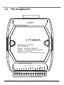
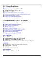
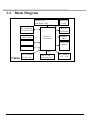
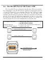
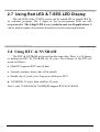
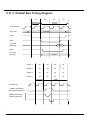
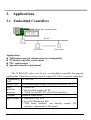
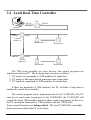
7188XA Series
Hardware User’s Manual
7000 New Features
1. Self Tuner Inside
Your Powerful Tools
2. Multiple Baud Rate
3. Multiple Data Format
Create New Ideas
4. Dual WatchDog Inside
5. True Distributed Control
Create New Applications
6. High Speed & High Density I/O
Warranty
All products manufactured by ICP DAS are warranted against defective
materials for a period of one year from the date of delivery to the original
purchaser.
Warning
ICP DAS assume no liability for damages consequent to the use of this
product. ICP DAS reserves the right to change this manual at any time without
notice. The information furnished by ICP DAS is believed to be accurate and
reliable. However, no responsibility is assumed by ICP DAS for its use, nor
for any infringements of patents or other rights of third parties resulting from
its use.
Copyright
Copyright 2000 by ICP DAS. All rights are reserved.
Trademark
The names used for identification only may be registered trademarks of their
respective companies.
7188XA Series Hardware User’s Manual, Ver. 3.0 May/2005, 7Mh-001-20 -----1
Table of Contents
1.
INTRODUCTION........................................................................................................................................................ 3
1.1
FEATURES .................................................................................................................................................................. 6
1.2
PIN ASSIGNMENT ..................................................................................................................................................... 10
1.3
SPECIFICATIONS ....................................................................................................................................................... 12
1.4
BLOCK DIAGRAM ..................................................................................................................................................... 14
1.5
WIRING DIAGRAMS FOR APPLICATION..................................................................................................................... 15
1.6
COMPARISON TABLE ................................................................................................................................................ 20
1.7
JUMPER SETTING ...................................................................................................................................................... 24
2.
OPERATION PRINCIPLES .................................................................................................................................... 25
2.1
SYSTEM MAPPING .................................................................................................................................................... 25
2.2
HOW TO DEBUG USER’S PROGRAMS ........................................................................................................................ 27
2.3
HOW TO DOWNLOAD USER’S PROGRAM .................................................................................................................. 28
2.4
USING THE DOWNLOAD_PORT AS A COM PORT ....................................................................................................... 28
2.5
COM PORTS COMPARISON....................................................................................................................................... 29
2.6
THE RS-485 PORT & SELF-TUNER ASIC................................................................................................................. 30
2.7
USING RED LED & 7-SEG LED DISPLAY............................................................................................................... 31
2.8
USING RTC & NVSRAM........................................................................................................................................ 31
2.9
USING EEPROM ..................................................................................................................................................... 32
2.10
USING THE WATCHDOG TIMER ................................................................................................................................ 32
2.11
USING THE I/O EXPANSION BUS .............................................................................................................................. 33
3.
APPLICATIONS ....................................................................................................................................................... 42
3.1
EMBEDDED CONTROLLERS ...................................................................................................................................... 42
3.2
LOCAL REAL TIME CONTROLLER............................................................................................................................. 43
3.3
REMOTE LOCAL CONTROLLER ................................................................................................................................. 44
3.4
I/O EXPANSION OF PLC APPLICATIONS ................................................................................................................... 45
3.5
RADIO MODEM APPLICATIONS ................................................................................................................................ 46
3.6
USING 4 COM PORT APPLICATION-1 ....................................................................................................................... 47
3.7
USING 4 COM PORT APPLICATION-2 ....................................................................................................................... 48
7188XA Series Hardware User’s Manual, Ver. 3.0 May/2005, 7Mh-001-20 -----2
1.
Introduction
The 7188XA(D) is a series of expandable embedded controllers designed
for industry applications. They can be used to replace the PC or PLC in harsh
environments. The 7188X series can be ordered as following:
Order Items
Module name
O. S.
7188XA(D)
Expandable Embedded controller
MiniOS7
7188XB(D)
Expandable Embedded controller
MiniOS7
7188XC(D)
Expandable Embedded controller
MiniOS7
7XXX
7XXX without 7-SEG display
MiniOS7
7XXXD
7XXX with 7-SEG display
MiniOS7
The 7000 series modules have been very successful during the past three
years. Over one hundred thousand modules have been shipped to locations all
over the world. The reasons for our success are given as follows:
Time-to-market & cost-effective solutions
Durable, stable, flexible, & easy to program
Over 50 various I/O modules are supported
Can be used in harsh, noisy industry environments
However, even though the 7000 family is so versatile, there are some
applications that cannot be initially solved, such as:
High speed applications
Special hardware requirement applications
Special software requirement applications
A combinations of special hardware & software applications
Therefore, we developed an I/O expansion bus for the 7188X family to
7188XA Series Hardware User’s Manual, Ver. 3.0 May/2005, 7Mh-001-20 -----3
solve all the above applications above. The I/O expansion bus can be used to
implement various I/O functions such as D/I, D/O, A/D, D/A, Timer/Counter,
UART, flash memory, battery backup SRAM, AsicKey & other I/O functions.
Nearly all kinds of I/O functions can be implemented by this bus.
The I/O expansion bus includes serial & parallel interface. The parallel
interface is very similar to ISA bus, so the user can move the old ISA bus
design to the I/O expansion bus with very little modification.
Furthermore, the I/O pins of the serial bus are programmable. They can be
programmed as D/I, or D/O. Some pins can be configured to D/I or D/O or
timer input or timer output. There are many serial interface devices today. The
features of these serial devices are given as follows:
Smaller size compared to parallel devices
Lower cost compared to parallel devices
Easier to design for isolation applications
The serial interface of the I/O expansion bus can link to these serial
devices very easily. The design of the I/O Expansion Bus makes the idea of a
“Customized 7000 Module” come true. The features of a “Customized 7000
Module” are given as follows:
7188XA(D)+X??
Single module solution
a “Customized 7000
Module”
7000 compatible command sets & RS-485 networking
Easy hardware/software interface for user to design & manufacture their
own special hardware & software
Time-to-market ODM solution for user’s special requirements (any high
speed, complex or combined functions of D/I/O, A/D, D/A,.., etc.)
Durable, stable, flexible, time-to-market & cost-effective total solution.
But the 7188X(A) don’t support the reconfiguration-resistor. So the userdefined pins of the 7188X family are given as follows:
7188XA Series Hardware User’s Manual, Ver. 3.0 May/2005, 7Mh-001-20 -----4
User defined pins
7188XA(D) 0
7188XB(D) 14
7188XC(D) 3
Reconfiguration pins
0
0
5
Customized I/O pins
0+0=0
14+0=14
3+5=8
Refer to “I/O Expansion Bus in 7188X/7188E User’s Manual” for more
information.
Refer to “7000 Bus Converter User Manual" chapter 1 for more information
as follows:
1.1
1.2
1.3
1.4
1.5
7000 Overview
7000 Related Documentation
7000 Common Features
7000 System Network Configuration
7000 Dimensions
Package List
In addition to this manual, the package includes the following items:
One 7188XA(D) hardware module
One hardware manual (this manual)
One release note
One software utility disk or CD
One download cable
CA0910 for 7188XA(D)
Note
If any of these items are missing or damaged, contact the local distributors for
more information. Save the shipping materials and cartons in case you want to
ship in the future.
Release Note
It is recommended to read the release note first. All important information will
be given in release note as follows:
• Where the “7188X/7521 Software User’s Manual” is
• Where the “I/O Expansion Bus for 7188X/7188E User’s Manual” is
• Where the software driver & diagnostic programs are
7188XA Series Hardware User’s Manual, Ver. 3.0 May/2005, 7Mh-001-20 -----5
1.1 Features
1.1.1
General features
AMD’s embedded CPU, Am188™ES: 40M
SRAM: 512K bytes
Flash ROM: 512K bytes
Built-in EEPROM
Built-in RTC&NVRam
Built-in COM port: COM1, COM2, COM3, COM4
Isolation voltage on RS-485 port=3000V
64-bit hardware unique serial number inside
User defined D/I/O
Built-in 5-digit LED display interface
COM driver support interrupt & 1K QUEUE input buffer
Built-in I/O expansion bus interface
Built-in watchdog timer for harsh environments
Built-in power protection circuit
Built-in RS-485 network protection circuit
Built-in self-tuner ASIC controller on RS-485 port
Program download from PC
Built-in OS: MiniOS7 of ICP DAS
Operating temperature: -25°C to +75°C
Can be used in harsh environments for industry applications
NOTE:
1. ODM wanted
2. “Customized 7000 Modules” wanted
7188XA Series Hardware User’s Manual, Ver. 3.0 May/2005, 7Mh-001-20 -----6
1.1.2
What is MiniOS7?
The MiniOS7 is an embedded O.S. designed for the 7188X/7521 series.
Developed by ICP DAS Co. Ltd; It is used to replace the ROMDOS used in
the 7188 series. Several brands of DOS have been created by various
companies. In all cases, DOS--whether PC-DOS, MS-DOS, or ROM-DOS--is
a set of commands or code which tells the computer how to process
information. DOS runs programs, manages files, controls information
processing, directs input and output, and performs many other related
functions. The MiniOS7 provides the equivalent functions of ROMDOS
while, in addition, providing user specific functions for the 7188X/7521
family.
Comparison table between MiniOS7 & ROM-DOS?
MiniOS7
ROMDOS
Power up time
0.1 sec
4 ~ 5 sec
More compact size
<64K bytes
64K bytes
Supports I/O expansion bus
Yes
No
Supports AsicKey
Yes
No
Flash ROM management
Yes
No
O.S. update (download)
Yes
No
Built-in hardware diagnostic functions
Yes
No
Direct control of the 7000 series modules
Yes
No
Customer ODM functions
Yes
No
Free charge
Yes
No
Note: We reserve the right to change the specifications of MiniOs7
without notice
7188XA Series Hardware User’s Manual, Ver. 3.0 May/2005, 7Mh-001-20 -----7
1.1.3 What is the 64-bit hardware unique serial number?
The 7188XA(D) equips a 64-bit hardware unique hardware serial number
onboard. This number is unique & cannot be shared by any two 7188XA(D)s.
The application software can check this number for illegal copies. It is the
most low cost protection mechanism the 7188XA(D) currently has.
1.1.4 What is the Self-Tuner ASIC?
The 2-wire RS-485 port is designed to directly drive the 7000 series
modules. It is a half-duplex 2-wire RS-485 network. Send/receive directional
control in a 2-wire RS-485 network is very important. Therefore, The
7188X/7521 series equip a Self-Tuner ASIC controller for all RS-485 ports.
The Self-Tuner ASIC controller will auto detect & control the send/receive
direction of the RS-485 network. Consequently, the application program does
not have to worry about the send/receive directional control of the RS-485
network.
1.1.5 What is the I/O Expansion Bus?
The 7188XA(D) support I/O expansion buses. The I/O expansion bus can be used to
implement various I/O functions such as D/I, D/O, A/D, D/A, Timer/Counter, UART,
flash memory, battery backup SRAM, AsicKey & other I/O functions. Nearly all kinds of
I/O functions can be implemented on this bus.
1.1.6 What is the AsicKey?
The I/O expansion bus supports AsicKey. The AsicKey equips a complex
machine for validation checking. Included in this is 128 bytes of private data
for the same purpose. It provides very strong protection against illegal copies.
Every legal user has a unique AsicKey & unique software library, the user can
self check this key, or the software library will check the key automatically. In
this main, it is nearly impossible to remove the AsicKey protection.
7188XA Series Hardware User’s Manual, Ver. 3.0 May/2005, 7Mh-001-20 -----8
1.1.7 7188XA(D) = Addressable RS-232 Converter?
The 7188XA(D) is designed as an embedded controller. Therefore, any
software can be downloaded into it. If the firmware for an ”Addressable RS232 Converter” is downloaded into a 7188XA(D), they will act as an
“Addressable RS-232 Converter”.
7188XA Series Hardware User’s Manual, Ver. 3.0 May/2005, 7Mh-001-20 -----9
1.2
Pin Assignment
COM1
i-7188XA
Embedded Controller
CPU 80188-40
COM1 : RS-232 / RS-485
COM2 : RS-485, 3000V Isolation
COM3~4 : RS-232
DI:3.5V~30V DO:100mA,30V max
COM4
COM3
COM2
7188XA Series Hardware User’s Manual, Ver. 3.0 May/2005, 7Mh-001-20 -----10
Pin assignment of 14-pin screw terminal block(7188XA/7188XAD):
Pin Name Description
1
DO1 100mA, 30Vmax.
2
DO2 100mA, 30Vmax.
3
DI1
3.5V ~ 30V
4
DI2
3.5V ~ 30V
5
RXD4 RXD pin of COM4 (RS-232)
6
TXD4 TXD pin of COM4 (RS-232)
7
GND GND pin of COM3 & COM4
8
TXD3 TXD pin of COM3 (RS-232)
9
RXD3 RXD pin of COM3 (RS-232)
10 INIT* Initial pin
11 D2+
DATA+ pin of COM2 (RS-485)
12 D2DATA- pin of COM2 (RS-485)
13 +VS
V+ of power supply (+10 to +30VDC unregulated)
14 GND GND of power supply
Note: COM3=(TXD3, RXD3, GND), COM4=(TXD4, RXD4, GND),
COM3&COM4 share the same GND-pin(pin 7)
Pin assignment of COM1 connector (DB-9 Male):
Pin Name Description
1
DCD Data Carrier Detect (RS-232)
2
RXD Receives Data
(JP1 select RS-232)
D1+
DATA+ of RS-485 (JP1 select RS-485)
3
TXD Transmits Data
(JP1 select RS-232)
D1DATA- of RS-485 (JP1 select RS-485)
4
DTR Data Terminal Ready (RS-232)
5
GND Signal ground of RS-232
6
DSR Data Set Ready (RS-232)
7
RTS
Request To Send (RS-232)
8
CTS
Clear To Send (RS-232)
9
RI
Ring Indicator (RS-232)
Note: The COM1 can be used as a RS-232 or RS-485 port selected by JP1.
Refer to Sec. 1.5 for JP1 settings. If JP1 is set in RS-232, the connector of
COM1 is the same as the DB-9 RS-232 connector of the PC. If JP1 is set in
RS-485, the COM1 can directly drive the 7000 series modules. Refer to Sec.
1.6.6 for wire connections.
7188XA Series Hardware User’s Manual, Ver. 3.0 May/2005, 7Mh-001-20 -----11
1.3 Specifications
General environment
Operating temperature: -25°C to +75°C
Storage temperature:-40°C to +85°C
Humidity: 0 to 90 %
Built-in Watch Dog Timer (1.6 seconds)
Built-in power protection & network protection circuit
Program downloadable from PC
Built-in I/O expansion bus interface
1.3.1 Specifications of 7188XA & 7188XAD
System
Module name: embedded controller
CPU: Am188™ES, 40M Hz
SRAM: 512K bytes
FLASH ROM: 512K bytes
COM port: COM1, COM2, COM3, COM4
Built-in RTC, NVRAM & EEPROM
Supports I/O Expansion Bus
Program download port: COM4
Real Time Clock
Year-2000 compliance
Seconds, minutes, hours, date of the month
Month, year, valid from 1980 to 2079
NVSRAM: 31 bytes, battery backup, data valid up to 10 years
EEPROM
2048 bytes ( 8 blocks, each block has 256 bytes)
Data retention > 100 years
1,000,000 erase/write cycles
D/I: 2 channels
High:3.5V ~ 30V, Low:0 ~ 1V
7188XA Series Hardware User’s Manual, Ver. 3.0 May/2005, 7Mh-001-20 -----12
D/O: 2 channels
100 mA, 30V max.
Flash Memory
512K bytes
Erase unit is one sector(64K bytes)
100,000 erase/write cycles
COM1
RS-232 or RS-485 jumper select(JP1), default is RS-232
RS-232: TXD,RXD,RTS,CTS,DTR,DSR,DCD,RI,GND
RS-485: D1+, D1-, self-tuner ASIC inside
Communication speed: 115200 max.
16 bytes FIFO
COM2
RS-485: D2+, D2-+, self-tuner ASIC inside
Communication speed: 115200 max.
16 bytes FIFO
Isolation voltage: 3000V
COM3
RS-232: TXD3, RXD3, GND
Communication speed: 115200 max.
COM4
RS-232: TXD4, RXD4, GND
Communication speed: 115200 max.
Program download port(default)
Can be used as general purpose RS-232 port
Display
7-segmemt LED: 5-digit (for 7188XAD)
Power
Power requirements: 10 to 30VDC(non-regulated)
Power consumption: 2.0W for 7188XA
3.0W for 7188XAD
7188XA Series Hardware User’s Manual, Ver. 3.0 May/2005, 7Mh-001-20 -----13
1.4
Block Diagram
SRAM=512K
Flash-ROM=512K
COM1
RS-232/RS-485
(selected by JP1)
COM2,RS-485
3000V isolation
Watchdog
circuit
RTC &
NVSRAM
80188-40
16 bits timer
COM3, RS-232
EEPROM
(2K)
5-digit LED
(options)
COM4, RS-232
+5V
7188XA
DO: 2 channels
150 mA, 30V
+10V to +30V
power converter
DI: 2 channels
3.5V ~ 30V
7188XA Series Hardware User’s Manual, Ver. 3.0 May/2005, 7Mh-001-20 -----14
1.5
Wiring Diagrams for Application
1.5.1 Program download
14
Ext. GND
+VS
13
Ext. 24V
D2-
12
D2+
11
Init*
10
RXD3
9
TXD3
8
GND
7
TXD4
6
RXD4
5
DI2
4
DI1
3
DO2
2
DO1
1
7188XA/7188XAD GND
1
DCD
2
Rxd/D+
3
Txd/D-
4
DTR
5
GND
6
DSR
7
RTS
8
CTS
9
RI
Connect INIT* to GND
to disable autoexec.bat
GND
TX
RX
Wire label of
CA0910
PC COM-1/2/3/4
RI
9
CTS
8
RTS
7
DSR
6
GND
5
DTR
4
TXD
3
RXD
2
DCD
1
Note:
Program
• There are 3 wires in the download cable
download
• Connect the wire-1, label RX, to pin-4 of 7188XA(D)
wire
• Connect the wire-2, label TX, to pin-5 of 7188XA(D)
connection
• Connect the wire-3, label GND, to pin-6 of 7188XA(D)
• Connect the DB-9 of download cable to PC COM-1/2/3/4 port
7188XA Series Hardware User’s Manual, Ver. 3.0 May/2005, 7Mh-001-20 -----15
1.5.2 Using a 3-wire RS-232 port
7188XA/7188XAD
RXD
TXD
GND
RS-232 Device
RI
CTS
RTS
DSR
GND
DTR
TXD
RXD
DCD
There are 3 wires as following:
• Connect RXD to TXD of RS-232 device
• Connect TXD to RXD of RS-232 device
• Connect GND to GND of RS-232 device
7188XA Series Hardware User’s Manual, Ver. 3.0 May/2005, 7Mh-001-20 -----16
1.5.3 Using a 5-wire RS-232 port
7188XA/7188XAD
RXD
TXD
GND
RTS
CTS
RS-232 Device
RI
CTS
RTS
DSR
GND
DTR
TXD
RXD
DCD
There are 5 wires as follows:
• Connect RXD to TXD of RS-232 device
• Connect TXD to RXD of RS-232 device
• Connect RTS to CTS of RS-232 device
• Connect CTS to RTS of RS-232 device
• Connect GND to GND of RS-232 device
7188XA Series Hardware User’s Manual, Ver. 3.0 May/2005, 7Mh-001-20 -----17
1.5.4 Using a 9-wire RS-232 port
7188XA/7188XAD
DCD
GND
14
Ext. GND
1
Rxd/D+
+VS
13
Ext. 24V
2
3
Txd/D-
4
DTR
5
GND
6
DSR
7
RTS
8
CTS
9
RI
5
1
6
2
232
COM1 = RS-232
Com1
modem
22 RI
5 CTS
4
RTS
6
DSR
7
GND
20 DTR
2 TXD
3
RXD
8
DCD
Note:
• The COM1 pin assignment of the 7188XA(D) is the same as the PC.
7188XA Series Hardware User’s Manual, Ver. 3.0 May/2005, 7Mh-001-20 -----18
1.5.5 Using a RS-485 port
7188XA/7188XAD GND
7000 module
14
Ext. GND
+VS
13
Ext. 24V
D2-
12
D2+
11
GND
10
Ext. GND
+VS
9
Ext. 24V
D2-
8
D2+
7
Note:
• The RS-485 interface can directly drive 256 sets of 7000 modules without a
repeater
7188XA Series Hardware User’s Manual, Ver. 3.0 May/2005, 7Mh-001-20 -----19
1.6
Comparison Table
7188XA
4500
Module name
Embedded Controller
PC-Based Communication Controller
CPU
AMD 80188, 40M Hz
AMD 80188, 40M Hz
SRAM
512K
256K
Flash ROM
512K
256K
O.S.
MiniOS7
ROM-DOS
COM port
4
2+1 (one for download only)
COM2 isolated
Yes
No
Self-tuner inside
Yes, Com1&Com2
No
EEPROM
2048 bytes
No
7-Seg LED
5-digit (7188XA(D)D)
No
I/O expansion bus
Yes
No
Support AsicKey
Yes
No
7521 series
4521
Module Name
Intelligent
Addressable
Communication Controller RS-232 Converter
CPU
AMD 80188, 20M Hz
MC68HC705, 3.68M Hz (8-bit uP)
Number of RS-232 devices 7521: 1 channel
able to handle
7522: 2 channels
7523: 3 channels
1
D/I
7521: 3 channels
7522: 3 channels
7523: 2 channels
0
D/O
7521: 3 channels
7522: 1 channel
0
Built-in program
Yes
Yes
Program Download
Yes
No
Modify program
Yes
No
7-Seg LED
7521D, 7522D, 7523D
No
I/O expansion bus
7521 & 7521D
No
Support AsicKey
7521 & 7521D
No
Isolation Site
On RS-485 site
On RS-232 site
Functions
Flexible
Limited
7188XA Series Hardware User’s Manual, Ver. 3.0 May/2005, 7Mh-001-20 -----20
Comparison table between the 7188 & the 7188X series:
7188(D)
7188XC(D)
7188XB(D)
7188XA(D)
CPU clock
80188, 40M Hz
80188,20M Hz
80188, 40M Hz
80188, 40M Hz
SRAM
256K
128K
256K
512K
Flash ROM
256K/512K
256K
(512K for ODM)
512K
512K
COM1
RS-232 with
modem control
or RS-485
RS-232
or RS-485 with
self-tuner inside
RS-232
or RS-485 with
self-tuner inside
RS-232 with
modem control
or RS-485 with
self-tuner inside
COM2
RS-485,
RS-485 with
self-tuner inside
RS-485 with
self-tuner inside
RS-485 with
self-tuner inside,
3000V isolation
COM3
RS-232 (txd,rxd)
No Com3
No Com3
RS-232 (txd,rxd)
COM4
RS-232 (txd,rxd)
No Com4
No Com4
RS-232 (txd,rxd)
User defined pins
0
3
14
0
Modem control
COM1
No
No
COM1
RTC
Yes
No
Yes
Yes
64 bits hardware
unique serial
number
No
No
Yes
Yes
EEPROM
2K bytes
2K bytes
2K bytes
2K bytes
D/I(3.5V~30V)
0
3 channels
1 channel
2 channels
D/O(150mA, 30V) 0
3 channels
1 channel
2 channels
I/O expansion bus
No
Yes
Yes
Yes
Support AsicKey
No
Yes
Yes
Yes
Operation system
MiniOS7
MiniOS7
MiniOS7
MiniOS7
Programming
language
TC/MSC/BC
TC/MSC/BC
TC/MSC/BC
TC/MSC/BC
COM1
COM1
COM4
Program download COM4
7188XA Series Hardware User’s Manual, Ver. 3.0 May/2005, 7Mh-001-20 -----21
Comparison table of 7188E series:
7188EA(D)
7188EX(D)
7188E2(D)
CPU clock
80188, 40M Hz
80188, 40M Hz
80188, 40M Hz
SRAM
512K
512K
256K
Flash ROM
512K
512K
256K
COM1
RS-232 or
RS-232 or
RS-232 or
RS-485 with
self-tuner inside
RS-485 with
self-tuner inside
RS-485 with
self-tuner inside
RS-485 with
RS-485 with
RS-485 with
self-tuner inside,
self-tuner inside,
self-tuner inside,
non-isolated
non-isolated
non-isolated
RTC
Yes
Yes
No
64 bits hardware
unique serial
number
Yes
Yes
No
EEPROM
2K bytes
2K bytes
2K bytes
D/I(3.5V~30V)
6 channels
0
0
D/O(150mA, 30V)
7 channels
0
0
User Defined pins
0
14
0
I/O expansion bus
Yes (but used by system)
Yes
No
Support AsicKey
Yes
Yes
No
Operation system
MiniOS7
MiniOS7
MiniOS7
Programming
language
TC/MSC/BC
TC/MSC/BC
TC/MSC/BC
Program download
COM1
COM1
COM1
Ethernet interface
10BaseT
10Base-T
10BaseT
COM2
7188XA Series Hardware User’s Manual, Ver. 3.0 May/2005, 7Mh-001-20 -----22
Comparison table of CPU modules:
Description
7188
Embedded Controller
7188XA
Expandable Embedded Controller with I/O Expansion Bus
7188XB
Expandable Embedded Controller with I/O Expansion Bus, high I/O expansion
7188XC
Expandable Embedded Controller with I/O Expansion Bus, low cost
7521/22/23
Embedded Communication Controller, 1/2/3 channels
7188EA
Embedded Internet/Ethernet Controller, DI * 6 channels, DO * 7 channels
7188EX
Embedded Internet/Ethernet Controller with I/O Expansion Bus
7188E1
Internet Communication Controller, RS232 * 1
7188E2
Internet Communication Controller, RS232 * 1 + RS485*1
7188E3
Internet Communication Controller, RS232 * 1 + RS485 * 1+RS422/485 * 1
+ DI * 4 +DO * 4
7188E4
Internet Communication Controller, RS232 * 3 + RS485*1
7188E5
Internet Communication Controller, RS232 * 4 + RS485*1
7188E8
Internet Communication Controller, RS232 * 7 + RS485*1
7188XA Series Hardware User’s Manual, Ver. 3.0 May/2005, 7Mh-001-20 -----23
1.7
Jumper Setting
The JP1 setting of the 7188XA/7188XAD are given as follows.
5
1
6
2
232
COM1 = RS-232 (default)
5
1
6
2
232
COM1 = RS-485
7188XA Series Hardware User’s Manual, Ver. 3.0 May/2005, 7Mh-001-20 -----24
2. Operation Principles
2.1 System Mapping
2.1.1
Address Mapping of the 7188XA(D) series
Device
Flash ROM
SRAM
COM1 BASE
COM2 BASE
COM3
COM4
Address mapping
512K: from 8000:0000 to F000: FFFF
512K: from 0000:0000 to 7000: FFFF
0x100
0x108
0XFF80 to 0XFF88
0XFF10 to 0XFF18
Interrupt No.
0
1
2
3
4
5
6
7
8
9
0A
0B
0C
0D
0E
0F
10
Interrupt mapping
Divided by zero
Trace
NMI
Break point
Detected overflow exception
Array bounds exception
Unused opcode exception
ESC opcode exception
Timer 0
Reserved
DMA-0
DMA-1
\INT0 of I/O expansion bus
\INT1 of I/O expansion bus
COM1
COM2
\INT4 of I/O expansion bus
7188XA Series Hardware User’s Manual, Ver. 3.0 May/2005, 7Mh-001-20 -----25
11
12
13
14
COM4
Timer 1
Timer 2
COM3
7188XA Series Hardware User’s Manual, Ver. 3.0 May/2005, 7Mh-001-20 -----26
2.2
How to Debug User’s Programs
The download_ports of the 7188XA(D) family are given as follows:
• 7188XA(D) Use COM4
When the 7188XA(D) family series is powered-up, it will initialize the
download_port to the following configuration:
• Start-bit=1, data-bit=8, stop-bit=1, no parity
• Baud rate = 115200 BPS
Then, the 7188XA(D) will send all power-up information to the
download_port. The user will see all power-up messages as follows:
• Power-off PC & 7188X
• Install the download cable between download_port of 7188XA(D) &
COM1 of PC (refer to Sec. 1.6)
• Power-up PC & Run 7188X.EXE
• Power-up 7188XA(D)
• All power-up message will be shown on the monitor of the PC
After the power-up stage, the 7188XA(D) will use the download_port as
its standard input/output. So the standard output of 7188X will be shown on
the PC’s monitor. If the user presses any key on the PC’s keyboard, this key
will be sent to the 7188X as standard input. Therefore the keyboard & monitor
of PC can be used as standard input & output of the7188XA(D) as follows:
• Use 7188X.EXE as a bridge between the 7188XA(D) & PC
• Run 7188X.EXE in PC to set up this bridge
• Keyboard of PC
standard input of 7188XA(D)
• Monitor of PC
standard output of 7188XA(D)
In this way, the 7188XA(D) can read data from the keyboard & display it
on the monitor. So program debugging will be more convenient & effective.
Note: 7188X.EXE is included on the companion floppy disk/CD.
7188XA Series Hardware User’s Manual, Ver. 3.0 May/2005, 7Mh-001-20 -----27
2.3 How to Download User’s Program
Refer to Sec. 2.2 to find the download_port first.
The user can download the program into the 7188XA(D) as follows:
• Power-off PC & the 7188XA(D)
• Install the download cable between download_port of the 7188XA(D) &
COM1 of PC (refer to Sec. 1.6)
• Power-up PC & Run 7188X.EXE
• Power-up the 7188XA(D)
• All power-up messages will be shown on the monitor of the PC
• Key-in “load”, press Enter key, & wait for system request message
• Press Alt-E, the screen will ask you to input filename,
• Key-in the filename & press Enter key, the file will be download into the
7188XA(D)
• Key-in the filename & press Enter. This will start to execute this file
• Pressing Alt & X at the same time will quit the 7188X.EXE
2.4 Using the download_port as a COM port
The user can use the download_port of the 7188XA(D) as a general purpose
RS-232 port as follows:
Download user’s program & autoexec.bat to the 7188XA(D) first.
Power off the 7188XA(D) & remove the download the cable from PC.
If they are connected, disconnect the INIT*-pin from GND-pin of the
7188XA(D)
Power on the 7188XA(D) (no standard input, no standard output, no debug
information)
Install the download cable between new RS-232 device & download_port
of the 7188XA(D)
Initialize the download_port to new configuration.
The download_port is a general purpose RS-232 port now.
Refer to “7188X/7521 Software User’s Manual” for demo programs
7188XA Series Hardware User’s Manual, Ver. 3.0 May/2005, 7Mh-001-20 -----28
2.5 COM ports Comparison
The COM port of the 7188XA(D) series can be RS-232 or RS-485 as follows:
type
Pins name
2-wire RS-485 Data+, Data3-wire RS-232 Txd,Rxd,Gnd
5-wire RS-232 Txd,Rxd,Gnd,Rts,Cts
9-wire RS_232 Txd,Rxd,Gnd,Rts,Cts,Dcd,Dtr,Dsr,Ri
The COM ports of the 7188XA(D) are given as follows:
COM port Hardware
COM1
16C550, 9-wire RS-232 or 2-wire RS-485
COM2
16C550, 2-wire RS-485
COM3
80188’s on-chip UART-0, 3-wire RS-232
COM4
80188’s on-chip UART-1, 3-wire RS-232
The programming of the 16C550 is very different from the 80188’s
UART. The interrupt handling of the 80188 is also very different from the
PC’s 8259. Therefore if the user downloads the PC’s RS-232 application
program into the 7188XA(D), it will not work.
The software driver of the 7188XA(D) is an interrupt driven library that
provides a 1K QUEUE buffer for every COM port. The software is well
designed & easy to use.
The software driver provides the same interface for all 4 COM ports. The
user can use these COM port in the same way without any difficulty.
7188XA Series Hardware User’s Manual, Ver. 3.0 May/2005, 7Mh-001-20 -----29
2.6 The RS-485 Port & Self-Tuner ASIC
The 2-wire RS-485 port is designed to directly drive 7000 series modules.
It is a half-duplex 2-wire RS-485 network. Send/receive directional control in
a 2-wire RS-485 network is very important. Therefore, the 7188X series equip
a Self-Tuner ASIC controller for all RS-485 ports. The Self-Tuner ASIC
controller will auto detect & control the send/receive direction of the RS-485
network. In this main, the application program does not have to worm about
the send/receive direction control of the RS-485 network. For example, the
software program for one-to-one communication is nearly the same.
ToCom(port, sent_data);
/* send one sent_char to RS-232/RS-485 */
*/
/* no direction control
while IsCom(port);
/* wait one echo_char from RS-232/RS-485 */
echo_data=ReadCom(port); /* read this echo_data
*/
RS-232
TXD, RXD, GND
7188XA
7188XA
RS-485
Data+, Data-
7188XA
7188XA
Self-Tuner ASIC
2-wire RS-485 network
Inside
Send/receive direction
Auto detect/control
7188XA Series Hardware User’s Manual, Ver. 3.0 May/2005, 7Mh-001-20 -----30
2.7 Using Red LED & 7-SEG LED Display
The red LED of the 7188XA series can be turned-ON or turned-OFF by
its software program. The 5 digits of the seven-segment LED are also
programmable. The 5-digit LED is very useful in real world applications. It
can be used to replace the monitor & touch-screen for many applications.
2.8 Using RTC & NVSRAM
The RTC & NVSRAM are located on the same chip. There is a Li-battery
to backup the RTC & NVSRAM for 10 years. The features of the RTC are
given as follows:
• MiniOS7 supports RTC time & date
• Seconds, minutes, hours, date of the month
• Month, day of week, year, Leap year valid up to 2079
NVSRAM: 31 bytes, data valid for 10 years
Note1: only 7188XA(D) & 7188XB(D) support RTC & NVRAM.
7188XA Series Hardware User’s Manual, Ver. 3.0 May/2005, 7Mh-001-20 -----31
2.9 Using EEPROM
The EEPROM is designed to store the data which is not changed very
frequently. This data is given as follows:
Module ID, configuration settings
COM port configuration settings
Small databases
The erase/write cycle of the EEPROM is limited, the user should not change
the EEPROM frequently for testing. The EEPROM can erase/write in single
byte, so it is very useful in real world applications.
2.10 Using the Watchdog Timer
The watchdog timer of the 7188XA(D) series is fixed at 1.6 sec. When the
7188XA(D) is powered up, the watchdog timer will be always enabled. If
the 7188XA(D) do not refresh the watchdog timer every 1.6 seconds, the
watchdog will RESET the 7188XA(D).
The MiniOS7 of the 7188XA(D) will automatically refresh the watchdog after
power up. The user program can call the software driver to tell MiniOS7 to
stop refreshing the watchdog timer, then the user program must refresh the
watchdog timer. If the user program does not refresh the watchdog timer every
1.6 seconds, the watchdog timer will RESET the 7188XA(D).
7188XA Series Hardware User’s Manual, Ver. 3.0 May/2005, 7Mh-001-20 -----32
2.11 Using the I/O Expansion Bus
The 7000 series modules have been very successful in during the past
three years. Over one hundred thousand modules have been shipped to
locations all over the world. The reasons for our success is given as follows:
Time-to-market & Cost effective solutions
Durable, Stable, Flexible & Easy programming
Over 50 Various I/O Modules are supported
Can be used in harsh & noisy industry environments
However, even though the 7000 family is so versatile, there are some
applications that cannot be solved. These applications are given as follows:
High speed applications
Special hardware requirement applications
Special software requirement applications
A combination of special hardware & software applications
Therefore, we developed an I/O expansion bus for the 7188X family to
solve all the above applications. The I/O expansion bus can be used to
implement various I/O functions such as D/I, D/O, A/D, D/A, Timer/Counter,
UART, flash memory, battery backup SRAM, AsicKey & other I/O functions.
Nearly all kinds of I/O functions can be implemented by this bus.
The I/O expansion bus includes serial & parallel interface. The parallel
interface is very similar to ISA bus, so the user can move the old ISA bus
design to the I/O expansion bus with very little change.
The I/O pins of serial bus are programmable. They can be programmed as
D/I, or D/O. Some pins can be configured to D/I or D/O or timer input or timer
output. There are many serial interface devices available today. The features of
these serial devices are given as follows:
Smaller size compared to parallel devices
Lower cost compared to parallel devices
Easier to design for isolated applications
The serial interface of the I/O expansion bus make interface to these serial
devices very easy.
7188XA Series Hardware User’s Manual, Ver. 3.0 May/2005, 7Mh-001-20 -----33
The combination of serial & parallel interface make the I/O expansion bus
very convenient & powerful for various industry applications. There are many
design examples given in “I/O Expansion Bus in the 7188X/7188E User’s
Manual”. All hardware circuit & software driver sources are OPEN for
modification. From these examples, the user can make new applications or
modify them for their special requirements. The system design steps are given
as follows:
Step 1: list all functions required
Step 2: for all functions, goto step 3. If all functions are solved STOP
Step 3: if this function can be solved by 7000 module goto step 2
Step 4: if this function can be solved by 7188X+X??? goto step 2
Step 5: user designed special hardware for I/O expansion bus
Step 6: user writes special software driver for this hardware
Step 7: combine the special hardware & software as a new module
Step 8: goto step 2
After the above steps, user can combine the standard 7000 modules &
special modules to solve all applications in the same RS-485 network. The
system is given as following:
7520
RS232
RS485
Host PC
RS485
Standard 7000 module
Standard 7000 module
RS485
Customized 7000 module
(7188X+X???)
Customized 7000 module
(7188X+X???)
7188XA Series Hardware User’s Manual, Ver. 3.0 May/2005, 7Mh-001-20 -----34
2.11.1
Definition of an I/O Expansion Bus
The I/O expansion bus of the 7188XA(D) series can be divided into 3
groups as follows:
1. Power supply & reset signals: VCC, GND, RESET, /RESET
2. , Parallel Bus:
•
System clock: CLOCKA
•
Asynchronous ready control: ARDY
•
Address bus: A0 ~ A6, A7 (7188XC series without A7)
•
Data bus: D0 ~ D7
•
Interrupt control: INT0, INT1, INT4 (7188XC series without INT4)
•
Chip select & read/write strobe: /CS, /WR, /RD
3. Serial Bus: TO_0, TO_1, TI_0, TI_1, SCLK, DIO9, DIO4, DIO14
Refer to “I/O Expansion Bus for 7188X/7188E User’s Manual” for more information.
7188XA Series Hardware User’s Manual, Ver. 3.0 May/2005, 7Mh-001-20 -----35
2.11.2 Definition
The definition of the I/O expansion bus is given as follows:
JP1 pin definition & description:
No
Name
Description
1
GND
Ground of PCB
2
GND
Ground of PCB
3
CLOCKA
Synchronous clock output of CPU
4
ARDY
Asynchronous ready input (level sensitive, OPEN=ready)
5
INT0
Interrupt request input of channel 0(asynchronous, active high)
6
INT1
Interrupt request input of channel 1(asynchronous, active high)
7
VCC
Power supply of PCB
8
RESET
Power up reset pulse (active high)
9
GND
Ground of PCB
10
/RESET
Power up reset pulse (active low)
11
TO_0
Timer output 0 of CPU (can be used as programmable D/I/O)
12
TO_1
Timer output 1 of CPU (can be used as programmable D/I/O)
13
TI_0
Timer input 0 of CPU (can be used as programmable D/I/O)
14
TI_1
Timer input 1 of CPU (can be used as programmable D/I/O)
15
SCLK
Common serial clock output of 7188 series
16
DIO9
Programmable D/I/O bit
17
DIO4
Programmable D/I/O bit
18
DIO14
Programmable D/I/O bit
19
VCC
Power supply of PCB
20
VCC
Power supply of PCB
•
•
•
•
•
•
CLOCKA:40M for 7188XA(D)
ARDY: leave this pin OPEN for no wait states applications
INT0, INT1: leave these two pins OPEN for no interrupt applications
TO_0, TO_1: can be used as CPU’s timer output or programmable D/I/O
TI_0, TI_1: can be used as CPU’s timer input or programmable D/I/O
DIO4, DIO9, DIO14: programmable D/I/O bit
•
SCLK: the 7188X/7188E series use this signal as a CLOCK source to drive all on-board
serial devices, so it is always programmed as D/O. Changing this signal to other
configurations will cause serious errors. User can use this signal to drive external serial
devices without any side effects.
7188XA Series Hardware User’s Manual, Ver. 3.0 May/2005, 7Mh-001-20 -----36
JP2 pin definition & description:
No
Name
Description
1
A0
Address bus
2
D0
Data bus
3
A1
Address bus
4
D1
Data bus
5
A2
Address bus
6
D2
Data bus
7
A3
Address bus
8
D3
Data bus
9
A4
Address bus
10
D4
Data bus
11
A5
Address bus
12
D5
Data bus
13
A6
Address bus
14
D6
Data bus
15
A7 or N/C
This pin is reserved & must be N/C for 7188XC & 7521 series
16
D7
Data bus
17
INT4 or N/C
Interrupt request input of channel 4(asynchronous, active high), this pin is
reserved & must be N/C for 7188XC & 7521 series
18
/WR
Write strobe output (synchronous, active low)
19
/CS
Chip select output (synchronous, active low)
20
/RD
Read strobe output (synchronous, active low)
•
•
•
•
•
Address bus (output): A0 ~ A6, A7
Data Bus (tri-state, bi-direction): D0 to D7
INT4: leave this pin OPEN for no interrupt applications
/CS, /RD, /WR: These 3 signals will be synchronous to CLOCKA (in JP1.3) & asynchronous to
ARDY (JP1.4)
The CS\ will be active if program inport/outport from I/O address 0 to 0xff.
Refer to “I/O Expansion Bus in the 7188X/7188E User’s Manual” for more
information.
7188XA Series Hardware User’s Manual, Ver. 3.0 May/2005, 7Mh-001-20 -----37
2.11.3 Parallel Bus Timing Diagram
t1
t3
t2
t4
Data
Phase
Address
Phase
CLKOUTA
A12-A0
Address
/CS
/RD
D7-D0
(Read)
Data
/WR
D7-D0
(Write)
Data
Case 1
tw
tw
tw
t4
Case 2
t3
tw
tw
t4
Case 3
t2
t3
tw
t4
Case 4
t1
t2
t3
t4
Address
Phase
Data
Phase
CLKOUTA
ARDY (Normally
Not-Ready System)
ARDY (Normally
Ready System)
.
7188XA Series Hardware User’s Manual, Ver. 3.0 May/2005, 7Mh-001-20 -----38
2.11.4 I/O Expansion Boards
I/O expansion board for prototype & test:
Board
Descriptions
X000
Prototype Board ( Small size)
XA/XC
X001
Prototype Board ( Large size)
XA/XC
X002
Prototype Board
XA/XB/XC/EX
X003
Self-test board for 7188XC
XC
X004
Self-test board for 7188XB/EX
XB/EX
X005
Prototype Board ( small size)
XB/EX
X006
Prototype Board ( Large size)
XB/EX
More…...
I/O expansion board for D/I, D/O, D/I/O, or Timer/Counter :
X100
8 channels of D/I, 3.5V~30V
XC
X101
8 channels of D/O, TTL(64mA)
XC
X102
2 channels of relay output
XC
X103
7 channels of isolated D/I(3.5V ~ 30V)
XC
X104
8 channels of D/I/O(single channel programmable)
XC
X105
8 channels of D/I/O(8-channel programmable)
XC
X106
2*D/O or 3*D/I
XC
X107
6 channels of D/I + 7 channels of D/O
XB/XC
X400
3 channels 16-bit Timer/ Counter expansion Board
XC
More…...
I/O expansion board for A/D,D/A:
X200
1 channel of 12-bit A/D(0~2.5V)
XC
X201
4 channels of 12-bit A/D(0~20mA)
XC
X202
7 channels of 12-bit A/D(0~20mA)
XB/EX
X204
2 channels of 12-bit A/D(+/- 1V)
XC
X300
2 channels of 12-bit D/A(0~4.095V)
XC
X301
1 channel of 12-bit A/D(0~2.5V) and 1 channel of 12-bit
D/A(0~4.095V)
XC
X302
1 channel of 12-bit A/D(+/- 5V) and 1 channel of 12-bit D/A(+/5V)
XC
More…...
7188XA Series Hardware User’s Manual, Ver. 3.0 May/2005, 7Mh-001-20 -----39
I/O Expansion Board for A/D, D/A, D/I, D/O:
X203
2 channels of 12-bit A/D(0~20mA)
XB/EX
X303
1 channel of 12-bit A/D(+/- 5V) and 1 channel of 12-bit D/A(
+/- 5V)
XB/EX
X304
3 channels of 12-bit A/D(+/- 5V) and 1 channel of 12-bit D/A(
+/- 5V)
XB/EX
X305
7 channels of 12-bit A/D(+/- 5V) and 1 channel of 12-bit D/A(+/5V)
XB/EX
More…...
I/O Expansion Board for RS-232/422, D/I, D/O:
X500
1 channel of RS-232, modem control, 115.2K max.
XC
X501
1 channel of 4-wire RS-232 ( RTS, CTS, TXD, RXD), 115.2K
max
XC
X502
1 channel of 4-wire RS-232 ( RTS, CTS, TXD, RXD) &
1 channel of 2-wire RS-232 (TXD, RXD) ,115.2K max
XC
X503
1 channel of 4-wire RS-232 ( RTS, CTS, TXD, RXD), 115.2K
max
XB/EX
X504
1 channel of 4-wire RS-232 ( RTS, CTS, TXD, RXD) &
XB/EX
1 channel of 8-wire RS-232 ( RI,DCD,DTR,DSR,CTS,RTS, CTS,
TXD, RXD ) ,115.2K max
X505
1 channel of 4-wire RS-232 ( RTS, CTS, TXD, RXD), 115.2K
max
XB/EX
X506
1 channel of 2-wire RS-232 (TXD, RXD), 115.2K max
XB/EX
X507
1 channel of 4-wire RS-422/485 and DI/O (RXD3+, RXD3-,
TXD3+, RXD3-) , 115.2K max
XB/EX
X508
1 channel of 4-wire RS-232 and DI/O (RTX,CTX,TXD, RXD) ,
115.2K max
XB/EX
X509
1 channel of 2-wire RS-232 and DI/O (TXD, RXD), 115.2K max
XB/EX
X510
1 channel of 2-wire RS-232/485 and DI/O , RS-232(TXD, RXD) ,
RS-485(D+,D-),115.2K max
XB/EX
More…...
7188XA Series Hardware User’s Manual, Ver. 3.0 May/2005, 7Mh-001-20 -----40
I/O Expansion Board for storage devices:
X600/2
2M bytes NAND Flash
XA/XB/XC/EX
X600
4M bytes NAND Flash
XA/XB/XC/EX
X601
8M bytes NAND Flash
XA/XB/XC/EX
X602
16M bytes NAND Flash
XA/XB/XC/EX
X603
32M bytes NAND Flash
XA/XB/XC/EX
X607
128K battery backup SRAM
XA/XB/XC/EX
X608
512K battery backup SRAM
XA/XB/XC/EX
More…...
Refer to “I/O Expansion Bus in the 7188X/7188E User’s Manual” for more information.
7188XA Series Hardware User’s Manual, Ver. 3.0 May/2005, 7Mh-001-20 -----41
3. Applications
3.1 Embedded Controllers
MMICON (or PC or touch-screen)
RS-232
RS-485
7188XA
7000 module
7000 module
Applications:
4500 replacement & enhancement (not compatible)
PC-Based controller replacement
PLC replacement
Special controller replacement
The 7188XA(D) series can be use as embedded controller for general
applications. Therefore it can be used to replace PC, PLC or special controllers.
Programming TC/MSC/BC
Tool
Debug Tool Via standard input/output (keyboard & monitor of PC)
Man
• MMICON
Machine
• Keyboard & monitor of PC
Interface
• Touch Screen (RS-232 or RS-485 interface)
Program
Stored in Flash ROM
Input/Output • Onboard D/I or D/O
• From I/O Expansion Bus
• 7000 series modules, can directly control 256
modules = thousands of I/O points
7188XA Series Hardware User’s Manual, Ver. 3.0 May/2005, 7Mh-001-20 -----42
3.2 Local Real Time Controller
7520
RS-232
RS-485
Host PC
RS-485
RS-485
7188XA
(address-1)
RS-485
7000 module
7000 module
7000 module
7000 module
RS-485
7188XA
(address-n)
The 7000 series modules are slave devices; the control programs are
implemented in host PC. The working steps are given as follows:
1. PC sends out commands to 7000 modules for input data.
2. PC analyzes this input data & generates some output data
3. PC send out commands to 7000 modules for output data
If there are hundreds of 7000 modules, the PC will take a long time to
analyze & control these modules.
The control program can be implemented in a local 7188XA(D). The PC
only has to send control arguments to the 7188XA(D), the 7188XA(D) will
control the local 7000 modules based on these control arguments. In this way,
the PC can handle thousands of 7000 modules with the 7188XA(D).
Some control functions are timing critical. The local 7188XA(D) can handle
these functions without the PC in real time.
7188XA Series Hardware User’s Manual, Ver. 3.0 May/2005, 7Mh-001-20 -----43
3.3 Remote Local Controller
RS-232
Host PC
telephone line
RS-485
RS-232
7188XA
7000 module
7000 module
The control program is implemented in a local 7188XA(D). The
7188XA(D) will directly control the 7000 modules based on these control
arguments.
The PC can access the remote 7188XA(D) for the following items:
Query & record the remote system status
Download the control arguments to remote 7188XA(D)
The remote 7188XA(D) can communicate to the PC for the following
items:
Emergency events call back
Remote system status send back
7188XA Series Hardware User’s Manual, Ver. 3.0 May/2005, 7Mh-001-20 -----44
3.4 I/O Expansion of PLC applications
PLC
COM1:RS-232
COM2:RS-485
7188XA
7000 series
There is a Man Machine Interface in most PLCs. This interface is
originally designed for MMI applications. The 7188XA(D) can use this
interface to build a bridge between PLC & 7000 modules.
The 7188XA(D) can directly read/write the internal memory of the PLC.
Therefore the PLC can access the 7000 input modules as follows:
1. The 7188XA(D) sends commands to the 7000 input modules
2. The 7188XA(D) writes this data to the PLC’s internal memory
3. The PLC accesses this data from the internal memory
The PLC can control the 7000 output modules as follows:
1. The PLC writes data to its internal memory
2. The 7188XA(D) reads this output data from the PLC’s memory
3. The 7188XA(D) sends commands to the 7000 output modules
In this way, the input data of the 7000 modules can be shown on the
touch screen. Also, the user can control the output of the 7000 modules from
the touch screen.
7188XA Series Hardware User’s Manual, Ver. 3.0 May/2005, 7Mh-001-20 -----45
3.5 Radio Modem Applications
Configuration 3
Point to multi-point application
Device A
Device C
SST-900/SST-2400 setting:
(Device A)
RS-232
Half-duplex mode
Synchronous way
Slave state
Baud rate=9600
Channel=3
Frequency=915.968MHz
The 7188XA series is a embedded
controller. Because the 7188XA series
is programmable, it can be used as a
bridge between the SST-900 &
external devices. These devices can
be PLC, controller or 7000 modules.
Device B
Device D
SST-900/SST-2400 setting:
(Device B/C/D)
RS-485 or RS-232
Half-duplex mode
Synchronous way
Slave state
Baud rate=9600
Channel=3
Frequency=915.968MHz
7188XA Series Hardware User’s Manual, Ver. 3.0 May/2005, 7Mh-001-20 -----46
3.6
Using 4 COM port Application-1
COM1:RS-232
PC
PLC
COM4:RS-232
COM3:RS-232
COM2:RS-485
7188XA
MMICON
7000 Series
SST-900/SST-2400
Radio Modem
SST-900/SST-2400
Radio Modem
7000 series
COM1: PLC can access the I/O states of 7000 modules
COM2: Directly controls the 7000 input/output modules
COM3: MMICON is used as the local MMI
COM4: PC is used to monitor & record the system data.
7188XA Series Hardware User’s Manual, Ver. 3.0 May/2005, 7Mh-001-20 -----47
3.7 Using 4 COM port Application-2
Modem
COM4: RS-232
Card Reader
COM1: RS-232
COM3: RS-232
7188XA
TOUCH-200
touch screen
COM2: RS-485
7000 Series
COM1: link to remote host PC
COM2: Directly controls the 7000 input/output modules
COM3: TOUCH-200 is used as the local MMI
COM4: Card reader is used as standard input device.
7188XA Series Hardware User’s Manual, Ver. 3.0 May/2005, 7Mh-001-20 -----48