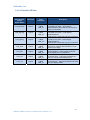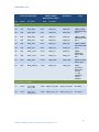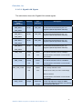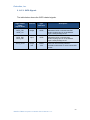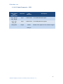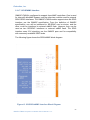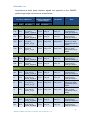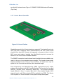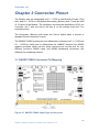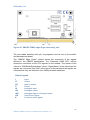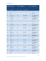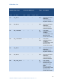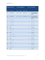
1
Embedian, Inc. SMARC Computer on Module Freescale i.MX6 Cortex A9 24bits Parallel LCD/LVDS/HDMI 4 x COM Ports 2 x SDHC 1 x USB Host 2.0, 1 x USB OTG 1 x 10/100/1000M Gigabit Ethernet 2 x CAN Bus, 2 x SPIs, 4 x I2Cs 1 x PCIe, 1 x SATA, 1 x MIPI SMARC-FiMX6 1 SMARC-FiMX6 Computer on Module User’s Manual v.1.2 Embedian, Inc. 2 SMARC-FiMX6 Computer on Module User’s Manual v.1.2 Embedian, Inc. Revision History Revision Date Changes from Previous Revision 1.0 2014/11/20 Initial Release 1.2 2015/2/25 Documentation Wording Fixed and add section 2.1.8 and add Ethernet MAC EEPROM information 3 SMARC-FiMX6 Computer on Module User’s Manual v.1.2 Embedian, Inc. USER INFORMATION About This Manual This document provides information about products from EMBEDIAN, INC. No warranty of suitability, purpose, or fitness is implied. While every attempt has been made to ensure that the information in this document is accurate, the information contained within is supplied “as-is” and is subject to change without notice. For the circuits, descriptions and tables indicated, EMBEDIAN assumes no responsibility as far as patents or other rights of third parties are concerned. Copyright Notice Copyright © 2014 EMBEDIAN, INC.. All rights reserved. No part of this manual may be reproduced, transmitted, transcribed, stored in a retrieval system, or translated into any language or computer language, in any form or by any means (electronic, mechanical, photocopying, recording, or otherwise), without the express written permission of EMBEDIAN. Trademarks The following lists the trademarks of components used in this board. ARM is a registered trademark of ARM Limited. Android is a registered trademark of Google Linux is a registered trademark of Linus Torvalds. WinCE is a registered trademark of Microsoft TI is a registered trademark of Texas Instruments All other products and trademarks mentioned in this manual are trademarks of their respective owners. Standards EMBEDIAN is ISO 9001:2008 and ISO14001-certified manufacturer. SMARC is an SGET standard for ARM computer on module. Warranty This EMBEDIAN product is warranted against defects in material and workmanship for the warranty period from the date of shipment. During the warranty period, EMBEDIAN will at its discretion, decide to repair or replace defective products. Within the warranty period, the repair of products is free of charge as long as warranty conditions are observed. The warranty does not apply to defects resulting from improper or inadequate maintenance or handling by the buyer, unauthorized modification or misuse, operation outside of the product’s environmental specifications or improper installation or maintenance. 4 SMARC-FiMX6 Computer on Module User’s Manual v.1.2 Embedian, Inc. EMBEDIAN will not be responsible for any defects or damages to other products not supplied by EMBEDIAN that are caused by a faulty EMBEDIAN product. Technical Support Technicians and engineers from EMBEDIAN and/or its subsidiaries and official distributors are available for technical support. We are committed to making our product easy to use and will help you use our products in your systems. Before contacting EMBEDIAN technical support, please consult our Web site for the latest product documentation, utilities, and drivers. If the information does not help solve the problem, contact us by e-mail or telephone. 5 SMARC-FiMX6 Computer on Module User’s Manual v.1.2 Embedian, Inc. Table of Contents CHAPTER 1 INTRODUCTION.............................................................................................................. 10 1.1 FEATURES AND FUNCTIONALITY ............................................................................................... 10 1.2 MODULE VARIANT ......................................................................................................................... 12 1.3 BLOCK DIAGRAM .......................................................................................................................... 13 1.4 SOFTWARE SUPPORT / HARDWARE ABSTRACTION.................................................................. 14 1.5 DOCUMENT AND STANDARD REFERENCES.............................................................................. 14 CHAPTER 2 SPECIFICATIONS ............................................................................................................ 18 2.1 SMARC-FIMX6 GENERAL FUNCTIONS ....................................................................................... 18 2.2 SMARC-FIMX6 DEBUG .................................................................................................................. 94 2.3 MECHANICAL SPECIFICATIONS.................................................................................................. 94 2.4 ELECTRICAL SPECIFICATIONS.................................................................................................. 109 2.5 ENVIRONMENTAL SPECIFICATIONS ......................................................................................... 114 CHAPTER 3 CONNECTOR PINOUT .................................................................................................. 116 3.1 SMARC-FIMX6 CONNECTOR PIN MAPPING ............................................................................ 116 CHAPTER 4 POWER CONTROL SIGNALS BETWEEN SMARC-FIMX6 MODULE AND CARRIER147 4.1 SMARC-FIMX6 MODULE POWER .............................................................................................. 147 4.2 POWER SIGNALS .......................................................................................................................... 152 4.3 POWER FLOW AND CONTROL SIGNALS BLOCK DIAGRAM .................................................. 156 4.4 POWER STATES ............................................................................................................................. 158 4.5 POWER SEQUENCES ................................................................................................................... 159 4.6 TERMINATIONS ............................................................................................................................ 163 4.7 BOOT DEVICE SELECTION ......................................................................................................... 167 6 SMARC-FiMX6 Computer on Module User’s Manual v.1.2 Embedian, Inc. Using this Manual This guide provides information about the Embedian SMARC-FiMX6 for Freescale i.MX6 embedded SMARC core module family. Conventions used in this guide This table describes the typographic conventions used in this guide: This Convention Is used for Italic type Emphasis, new terms, variables, and document titles. Filenames, pathnames, and code examples. monospaced type Embedian Information Document Updates Please always check the product specific section on the Embedian support website at www.embedian.com/ for the most current revision of this document. Contact Information For more information about your Embedian products, or for customer service and technical support, contact Embedian directly. To contact Embedian by Use Mail Embedian, Inc. 4F-7. 432 Keelung Rd. Sec. 1, Taipei 11051, Taiwan World Wide Web http://www.embedian.com/ Telephone + 886 2 2722 3291 Additional Resources Please also refer to the most recent Freescale i.MX6 processor reference 7 SMARC-FiMX6 Computer on Module User’s Manual v.1.2 Embedian, Inc. manual and related documentation for additional information. 8 SMARC-FiMX6 Computer on Module User’s Manual v.1.2 Embedian, Inc. Introduction This Chapter gives background information on the SMARC-FiMX6 Section include: Features and Functionality Module Variant Block diagram Software Support / Hardware Abstraction Module Variant Document and Standard References 9 SMARC-FiMX6 Computer on Module User’s Manual v.1.2 Embedian, Inc. Chapter 1 Introduction The SMARC® (Smart Mobility ARChitecture) FiMX6 is a versatile small form factor Computer-On-Module with Freescale i.MX6 processor and offers a wide range of processor scalability with single, dual and quadcore processors. The X86 alike interfacing of SMARC-FiMX6 allows an easy integration in any kind of application. The module connector has 314 edge fingers that mate with a low profile 314 pin 0.5mm pitch right angle connector (this connector is sometimes identified as an 321 pin connector, but 7 pins are lost to the key). Featuring Freescale’s i.MX6 System-on-Chip, Embedian’s SMARC-FiMX6 offers 24-bit Parallel LCD, single- or dual-channel LVDS, Gigabit Ethernet, HDMI, SDHC, USB 2.0, USB OTG, four UARTs support and many peripheral interfaces in a cost effective, low power, miniature package. Embedian’s SMARC-FiMX6 thin and robust design makes it an ideal building block for reliable system design. The module is the ideal choice for a broad range of target markets including HVAC Building and Control Systems Rear seat and in-freight entertainment system. Smart Grid and Smart Metering Digital Signage HMI/ In-Home Display Smart Toll Systems Connected Vending Machines Display Unit General Control System And more Complete and cost-efficient Embedian evaluation kits for Yocto, Ubuntu 12.04, Android ICS and Microsoft Windows Embedded Compact 7 allow immediate and professional embedded product development with dramatically reduced design risk and time-to-market. 1.1 Features and Functionality The SMARC-FiMX module is based on the i.MX6 processor with solo, dual lite, dual and quad core from Freescale. This processor offers a high number of interfaces. The module has the following features: SMARC 1.0 or 1.1 compliant in an 82mm x 50mm form factor. 10 SMARC-FiMX6 Computer on Module User’s Manual v.1.2 Embedian, Inc. Processor: Freescale i.MX6 ARM Cortex-A9 up to 1GHz Memory: Onboard 4GB eMMC Flash and 4MB SPI NOR Flash Onboard 1GB or 2GB DDR3 Note 1 Networking: 1 x 10/100/1000 Mbps Ethernet Display: 24-bit Parallel LCD Single channel LVDS LCD 18 or 24 bit or dual channel LVDS HDMI Expansion: 2 x SDHC/SDIO, 1 x USB 2.0 Host USB: 1 x USB 2.0 Host, 1 x USB 2.0 OTG, 1 x PCIe A single 4KB EEPROM is provided on I2C0 that holds the board information. This information includes board name, serial number, and revision information. Additional Interface: 4 x UARTs 2 x SPI 4 x I2C 1 x I2S 2 x CAN Bus 1 x PWM 12 x GPIOs 1 x SATA (Dual and Quad only) WDT SW Support: L:inux, Yocto, Ubuntu, Android ICS, Windows Embedded Compact 7 Power Consumption (Typcal) Solo Core (512MB DDR3): 1.55 Watts Dual Lite Core (1GB DDR3): 2.2 Watts Dual Core (1GB DDR3): 2.5 Watts Quad Core (1GB DDR3): 3.6 Watts Thermal: o o Normal Temperature: 0 C ~ 60 C o o Industrial Temperature: -40 ~85 C Power Supply 3V to 5.25V (single 5V is recommended in non-battery operation) 3.3V or 1.8V module IO support Note1: SMARC-FiMX6-S (solo core) only has 512MB DDR3 on board SMARC-FiMX6-U (dual lite core) only has 1GB DDR3 memory on board (no 2GB option for this variant.) 11 SMARC-FiMX6 Computer on Module User’s Manual v.1.2 Embedian, Inc. 1.2 Module Variant The SMARC-FiMX6 module is available with various options based on processors in this family from Freescale, DDR3 memory configuration, voltage rail of VDDIO and operating temperature ranges. 1: 2: 3. 4. “S” (solo core running up to 1GHz) “U” (dual lite core running up to 1GHz) “D” (dual core running up to 1GHz) “Q” (quad core running up to 1GHz) “1G” (1GB DDR3 memory) “2G” (2GB DDR3 memory, only for dual and quad core) “P” (if 1.8V VDDIO) Leave it Blank if 3.3V VDDIO “I” (Industrial temperature (-40oC~85oC), CPU running up to 800MHz) Leave it Blank if normal temperature For example, SMARC-FiMX-D-1G stands for dual core i.MX6 processor running up to 1GHz with 1GB DDR3 memory in normal operating temperature. The VDDIO voltage rail is 3.3V (SMARC spec. 1.0 compliant). 12 SMARC-FiMX6 Computer on Module User’s Manual v.1.2 Embedian, Inc. 1.3 Block Diagram The following diagram illustrates the system organization of the SMARC-FiMX6. Arrows indicate direction of control and not necessarily signal flow. Figure 1: SMARC-FiMX6 Block Diagram Details for this diagram will be explained in the following chapters. 13 SMARC-FiMX6 Computer on Module User’s Manual v.1.2 Embedian, Inc. 1.4 Software Support / Hardware Abstraction The Embedian SMARC-FiMX6 Module is supported by Embedian BSPs (Board Support Package). The first SMARC-FiMX6 BSP targets Linux (Ubuntu 14.04 LTS and Yocto Project) and Android support. BSPs for other operating systems are planned. Check with your Embedian contact for the latest BSPs. This manual goes into a lot of detail on I/O particulars – information is provided on exactly how the various SMARC edge fingers tie into the Freescale i.MX6 SoC and to other Module hardware. This is provided for reference and context. Almost all of the I/O particulars are covered and abstracted in the BSP and it should generally not be necessary for users to deal with I/O at the register level. 1.5 Document and Standard References 1.5.1. External Industry Standard Documents eMMC (Embedded Multi-Media Card) the eMMC electrical standard is defined by JEDEC JESD84-B45 and the mechanical standard by JESD84-C44 (www.jedec.org). The I2C Specification, Version 2.1, January 2000, Philips Semiconductor (now NXP) (www.nxp.com). I2S Bus Specification, Feb. 1986 and Revised June 5, 1996, Philips Semiconductor (now NXP) (www.nxp.com). JTAG (Joint Test Action Group defined by IEEE 1149.1-2001 - IEEE Standard Test Access Port and Boundary Scan Architecture (www.ieee.org). MXM3 Graphics Module Mobile PCI Express Module Electromechanical Specification, Version 3.0, Revision 1.1, © 2009 NVIDIA Corporation (www.mxm-sig.org). PICMG® EEEP Embedded EEPROM Specification, Rev. 1.0, August 2010 (www.picmg.org). SD Specifications Part 1 Physical Layer Simplified Specification, Version 3.01, May 18, 2010, © 2010 SD Group and SD Card Association (Secure Digital) (www.sdcard.org). SPI Bus – “Serial Peripheral Interface” - de-facto serial interface standard defined by Motorola. A good description may be found on Wikipedia (http://en.wikipedia.org/wiki/Serial_Peripheral_Interface_Bus). USB Specifications (www.usb.org). Serial ATA Revision 3.1, July 18, 2011, Gold Revision, © Serial ATA 14 SMARC-FiMX6 Computer on Module User’s Manual v.1.2 Embedian, Inc. International Organization (www.sata-io.org) PCI Express Specifications (www.pci-sig.org) SPDIF (aka S/PDIF) (“Sony Philips Digital Interface)- IEC 60958-3 1.5.2. SGET Documents SMARC_Hardware_Specification_V1p0, version 1.0, December 20, 2012. SMARC_Hardware_Specification_V1p1, version 1.1, May 29, 2014. Smart Mobility Architecture Design Guide, version 1.0, July 9, 2013 Smart Mobility Architecture Design Guide, version 1.1, May 29, 2014 1.5.3. Embedian Documents The following documents are listed for reference. The Module schematic is not usually available outside of Embedian, without special permission. The other schematics will be available. Contact your Embedian representative for more information. The SMARC Evaluation Carrier Board Schematic is particularly useful as an example of the implementation of various interfaces on a Carrier board. SMARC Evaluation Carrier Board Schematic, PDF and OrCAD format SMARC Evaluation Carrier Board User’s Manual SMARC-FiMX6 User’s Manual SMARC-FiMX6 Schematic Checklist 1.5.4. Freescale Documents IMX6DQRM, i.MX 6Dual/6Quad Applications Processor Reference Manual, May 2014 (rev. 2) IMX6DQ6SDLHDG, Hardware Development Guide for i.MX 6Quad, 6Dual, 6DualLite, 6Solo Families of Applications Processors, June 2013 (rev. 1) AN4059, i.MX 6Dual/6Quad Power Consumption Measurement, Oct 2012 (rev. 0) 15 SMARC-FiMX6 Computer on Module User’s Manual v.1.2 Embedian, Inc. 1.5.5. Freescale Development Tools IOMUX_TOOL for ARM® i.MX6 Microprocessors IMX_CST_TOOL, Freescale Code Signing Tool for the High Assurance Boot library. 1.5.6. Freescale Software Documents L3.0.101_SOURCE_BSP, i.MX 6Quad, i.MX 6Dual, i.MX 6DualLite, i.MX 6Solo and i.MX 6Sololite Linux BSP Source Code Files. Nov 3, 2014 (Rev.# L3.0.101) Fsl-L3.10.17_1.0.2_iMX6QDLS_BUNDLE, i.MX 6Quad, i.MX 6Dual, i.MX 6DualLite, i.MX 6Solo Linux Binary Demo Files and Linux BSP Documentation. Oct. 29, 2014 (Rev.# L3.10.17) IMX6_JB43_110_ANDROID_SOURCE_BSP, i.MX 6Quad, i.MX 6Dual, i.MX 6DualLite, i.MX 6Solo and i.MX 6Sololite Android jb4.3_1.1.0 0 BSP, Documentation and Source Code for BSP and Codecs. Dec. 19, 2013 (Rev.# jb4.3_1.1.0) IMX6_KK442_100_ANDROID_SOURCE_BSP, i.MX 6Quad, i.MX 6Dual, i.MX 6DualLite, i.MX 6Solo and i.MX 6Sololite Android KK4.4.2_1.0.0 BSP, Source Code for BSP and Codecs. July 14, 2014 (Rev.# KK442.2_1.0.0) 1.5.7. Embedian Software Documents Embedian Linux BSP for SMARC-FiMX6 Module Embedian Android BSP for SMARC-FiMX6 Module Embedian Linux BSP User’s Guide Embedian Android BSP User’s Guide 1.5.8. Freescale Design Network SABRE Wandboard Nucleus QNX 16 SMARC-FiMX6 Computer on Module User’s Manual v.1.2 Embedian, Inc. Specifications This Chapter provides SMARC-FiMX6 specifications. Section include: SMARC-FiMX6 General Functions SMARC-FiMX6 Debug Mechanical Specifications Electrical Specification Environment Specification 17 SMARC-FiMX6 Computer on Module User’s Manual v.1.2 Embedian, Inc. Chapter 2 Specifications 2.1 SMARC-FiMX6 General Functions 2.1.1. SMARC-FiMX6 Feature Set This section lists the complete feature set supported by the SMARC-FiMX6 module. SMARC Feature Specification SMARC Specification Maximum Number Possible SMARC-FiMX6 Feature Support SMARC-FiMX6 Feature Support Instances LVDS Display Support 1 Yes 1 (18 or 24 bits)Note1 Parallel LCD Support 1 Yes 1 (24 bits) HDMI Display Support 1 Yes 1 CSI Camera Support (Dual and Quad lanes) 2 Yes 1 (Quad Lane) Serial Camera Support 2 Yes 1 (4 lanes) USB Interface 3 Yes 2 PCIe Interface 3 Yes 1 (one Lane) SATA Interface 1 Yes 1 (0 on Solo and DualLite) GbE Interface 1 Yes 1 SDIO Interface (4bit) 1 Yes 1 (max. 25MHz) SDMMC Interface (8bit) 1 Yes 1 (max. 25MHz) SPI Interface 2 Yes 2 I2S Interface 3 Yes 1 I2C Interface 5 Yes 5 Serial 4 Yes 4 CAN 2 Yes 2 18 SMARC-FiMX6 Computer on Module User’s Manual v.1.2 Embedian, Inc. SMARC Feature Specification SMARC Specification Maximum Number Possible SMARC-FiMX6 Feature Support AFB Yes I/O Voltage (1.8V) Level Support Yes I/O Voltage (3.3V) Level Support Yes SMARC-FiMX6 Feature Support Instances Dual Channel LVDS is realizedNote2 Note: 1. Single channel LVDS interface: 1 x 18 bpp OR 1 x 24 bpp (up to 85 MHz per interface e.g 1366x768 @ 60Hz + 35% blanking) 2. Dual channel LVDS interface: 2 x 18 bpp OR 2 x 24 bpp (up to 170 MHz pixel clock e.g 1600x1200 @ 60 Hz + 35% blanking). 2.1.2. Form Factor The SMARC-FiMX6 module complies with the SMARC General Specification module size requirements in an 82mm x 50mm form factor. 19 SMARC-FiMX6 Computer on Module User’s Manual v.1.2 Embedian, Inc. 2.1.3. CPU The SMARC-FiMX6 implements Freescale’s i.MX6 ARM processor. Freescale CPU i.MX6 Solo i.MX6 DualLite 1 2 2 4 1GHz 1GHz 1GHz 1GHz DDR3-400 DDR3-400 DDR3-533 DDR3-533 32-bit 64-bit 64-bit 64-bit 512KB L2 512KB L2 1MB L2 + VFPv3 1MB L2 + VFPv3 GFX Vivante Vivante Vivante Vivante GFX core frequency 528MHz 528MHz 528MHz 528Mhz IPUs 1 1 2 2 LVDS Single or Dual Channel (18-bot or 24-bit) Single or Dual Channel (18-bot or 24-bit) Single or Dual Channel (18-bot or 24-bit) Single or Dual Channel (18-bot or 24-bit) LVDS Resolutions Single channel LVDS interface : 1 x 18 bpp or 1 x 24 bpp (up to 85 MHz per interface e.g 1366x768 @ 60Hz + 35% blanking) Single channel LVDS interface : 1 x 18 bpp or 1 x 24 bpp (up to 85 MHz per interface e.g 1366x768 @ 60Hz + 35% blanking) Single channel LVDS interface : 1 x 18 bpp or 1 x 24 bpp (up to 85 MHz per interface e.g 1366x768 @ 60Hz + 35% blanking) Single channel LVDS interface : 1 x 18 bpp or 1 x 24 bpp (up to 85 MHz per interface e.g 1366x768 @ 60Hz + 35% blanking) Dual channel LVDS interface: 2 x 18 bpp OR 2 x 24 bpp (up to 170 MHz pixel clock e.g 1600x1200 @ 60 Hz + 35% blanking). Dual channel LVDS interface: 2 x 18 bpp OR 2 x 24 bpp (up to 170 MHz pixel clock e.g 1600x1200 @ 60 Hz + 35% blanking Dual channel LVDS interface: 2 x 18 bpp OR 2 x 24 bpp (up to 170 MHz pixel clock e.g 1600x1200 @ 60 Hz + 35% blanking Parallel LCD Resolutions 1920x1080x60 1920x1080x60 1920x1080x60 1920x1080x60 HDMI Resolutions 1920x1080x60 1920x1080x60 1920x1200x60 1920x1200x60 Cores ClockNote1 Memory Speed Memory Bus Cache i.MX6 Dual i.MX6 Quad Dual channel LVDS interface: 2 x 18 bpp OR 2 x 24 bpp (up to 170 MHz pixel clock e.g 1600x1200 @ 60 Hz + 35% blanking 20 SMARC-FiMX6 Computer on Module User’s Manual v.1.2 Embedian, Inc. Freescale CPU i.MX6 Solo i.MX6 DualLite i.MX6 Dual i.MX6 Quad 3D Graphics 1 shader 1 shader 4 shaders 4 shaders 2D Graphics X1 X1 X2 X2 Independent DisplayNote2 - - yes yes Note: 1. For industrial temp. boards, the clocking speed is only up to 800MHz. 2. The LVDS interface can be used either as a single channel or as a dual channel. It is also possible to use the LVDS interface as two independent single LVDS channels. To do this, it is recommended to configure the LVDS display in the bootloader. Three independent displays are possible when connected as two single LVDS channel and one HDMI interface. 2.1.4. Module Memory The SMARC-FiMX6 module supports different configurations of DDR3 memory. The following table shows the available options. SMARC Variants i.MX6 Solo i.MX6 DualLite i.MX6 Dual i.MX6 Quad 512MB DDR3 Yes No No No 1GB DDR3 No Yes Yes Yes 2GB DDR3 No No Yes Yes Check with your Embedian contact or on the Embedian web site for updated information. 21 SMARC-FiMX6 Computer on Module User’s Manual v.1.2 Embedian, Inc. 2.1.5. Graphic Core The integrated Vivante core based supports: 3D Graphic Core Vivante GC2000 Solo: 1 Core Shader Cores Dual Lite: 1 Core Dual: 4 Cores Quad: 4 Cores 2D Core Vivante GC320 2D Performance 633M pixels / sec raw performance Vector Graphics Core Vivante GC355 API (DirectX/OpenGL) OpenGL ES 1.1/2.0/3.0, OpenCL 1.1 EP, OpenVG 1.1 Encode: H.264 BP/CBP H.263 V2 MPEG-4 SP MPEG-2 Hardware Accelerated Video MJPEG Baseline Decode: MPEG2 MP/HP MPEG4/Xvid SP/ASP H.264 BP/MP/HP H.264 MVC BP/MP/HP H.263 V2 DivX v3/4/5/6 VC-1 SP/MP/AP MJPEG Baseline VP6/VebM VP8 22 SMARC-FiMX6 Computer on Module User’s Manual v.1.2 Embedian, Inc. 2.1.6. Onboard Storage The SMARC-FiMX6 module supports a 4GB eMMC flash memory device, 4MB SPI NOR flash and a 32Kb I2C serial EEPROM on the Module I2C_PM (I2C0) bus. The device used is an On Semiconductor 24C32 equivalent. The Module serial EEPROM is intended to retain Module parameter information, including a module serial number. The Module serial EEPROM data structure conforms to the PICMG® EEEP Embedded EEPROM Specification.). The onboard 4MB SPI NOR flash is used as SPI boot media. The module will always boot up from the onboard SPI NOR flash first. The firmware in NOR flash will read the configuration from the boot selection and boot up the devices from that selected. 2.1.7. Clocks A 32.768 KHz clock is required for the i.MX6 CPU RTC (Real Time Clock) and external (S-35390A) RTC. The Freescale i.MX6 CPU is provided with a 24 MHz clock using a crystal in normal oscillation mode (On-chip Oscillator). The Qualcomm AR8035 PHY is provided with a 24 MHz clock using a crystal in normal oscillation mode. 2.1.8. Multiple Displays with IPU in i.MX6 There are basically two limitations which have to be pointed out. IPU capabilities The two display ports (DI0 and DI1) of each IPU are limited to a combined pixel clock of 240MHz. The maximum clock for a single display port is 220MHz. This results in the following table (for one IPU only): 23 SMARC-FiMX6 Computer on Module User’s Manual v.1.2 Embedian, Inc. The table above only describes the capabilities of the display ports to perform screen refresh. A full use case typically includes additional activities like video processing, resizing etc., decreasing the possible display resolutions. LVDS Serialization Another limitation by using the LVDS interfaces is the maximum clock of the LVDS serializer. For single-channel output the pixel clock is limited to 85 MHz per LVDS port. This results in a maximum resolution of WXGA (1366x768 @ 60HZ with 35% blanking), for example. If a higher resolution is needed, the split mode has to be used. In this case one LVDS port outputs ODD data and the other port EVEN data. The pixel clock is limited to 170 MHz (e.g. UXGA 1600x1200 @ 60 Hz with 35% blanking). To use the split mode, you need a display supporting the dual channel LVDS mode in order to receive odd and even pixel data! 24 SMARC-FiMX6 Computer on Module User’s Manual v.1.2 Embedian, Inc. 2.1.9. Parallel LCD Interface The Freescale i.MX6 parallel 24 bit LCD interface is brought to the Module edge connector. The interface runs at the 3.3V or 1.8V Module I/O voltage depending on the part number that users select. The SMARC Module parallel LCD pins may be used to drive a traditional parallel LCD interface (or they may be used to drive LVDS transmitters or other transmitters that accept parallel LCD data at the Module VDD_IO level). For parallel displays with very small form factors (think cell phone and digital camera size), the data I/O level is usually 1.8V. For larger displays, the display will likely require a 3.3V data I/O level. If the SMARC modules are with 3.3V VDD_IO and parallel displays are with 3.3 V I/O, the SMARC Parallel LCD data signals may be passed directly to the display, for short cable runs. This voltage swing may be used directly with 3.3V capable Carrier Board LVDS transmitters, such as the TI SN75LVDS83B. The 3.3V signaling is suitable for direct connection to a parallel flat panel in most cases. Generally speaking, larger parallel LCD panels are likely to use 3.3V or 5V signaling. If LCD panels use 5V signaling, a set of voltage translators / buffers would be needed on the Carrier. If the SMARC modules are with 1.8V VDD_IO and parallel displays are with 1.8V I/O, the SMARC Parallel LCD data signals may be passed directly to the display, for short cable runs. For larger displays with 3.3V I/O level and the SMARC modules are 1.8V VDD_IO, a bus transceiver like TI SN74AVC32T245-ZKE is required to achieve signal buffering and voltage translation from VDD_IO to a 3.3V display. If there is a requirement for a display cable longer than a few inches, it may be a good idea to include the buffer even if the display accepts 1.8V I/O. The voltage swing may be used directly with 1.8V capable Carrier Board LVDS transmitters, such as TI DS90C185. The following figure shows the parallel LCD block diagram. 25 SMARC-FiMX6 Computer on Module User’s Manual v.1.2 Embedian, Inc. Figure 2: SMARC-FiMX6 Parallel LCD Diagram The mapping of the Freescale i.MX6 parallel LCD pins to the SMARC edge connector is shown in the table below. Basically, Freescale i.MX6 processor maps the 18 bits of R, G, B for 6 bit color depth to DISP0_DAT[23:18], DISP0_DAT[15:10] and DISP0_DAT[7:2]. For i.MX6, the extra bits used for a 24 bit color implementation come out on Freescale i.MX6 DISP0_DAT[17:16], DISP0_DAT[9:8] and DISP0_DAT[1:0]. Since 18-bit configuration and 24-bit configuration use the same MSB signals, we can say 18-bit configuration is higher bits subset 24-bit configuration from the hardware point of view. The SMARC golden fingert has the smae convention: Red is LCD_D[23:16]; Blue is LCD_D[15:8] and Green is LCD_D[7:0]. For 24 bit implementations, all bits are used. For 18 bit implementations, in SMARC, the least significant bits (Red LCD_D[17:16], Green LCD_D[9:8], Blue LCD_D[1:0]) are dropped. 26 SMARC-FiMX6 Computer on Module User’s Manual v.1.2 Embedian, Inc. SMARC-FiMX6 Edge Golden Finger Net Names (Carrier Board) Color 24-bit Color Map Ball Mode Pin Name Pin# Pin Name W24 ALT0 DISP0_DAT23__ IPU1_DISP0_DATA23 S118 LCD_D23 (MSB) LCD_D23 R7 V24 ALT0 DISP0_DAT22__ IPU1_DISP0_DATA22 S117 LCD_D22 LCD_D22 R6 T20 ALT0 DISP0_DAT21__ IPU1_DISP0_DATA21 S116 LCD_D21 LCD_D21 R5 U22 ALT0 DISP0_DAT20__ IPU1_DISP0_DATA20 S115 LCD_D20 LCD_D20 R4 U23 ALT0 DISP0_DAT19__ IPU1_DISP0_DATA19 S114 LCD_D19 LCD_D19 R3 V25 ALT0 DISP0_DAT18__ IPU1_DISP0_DATA18 S113 LCD_D18 LCD_D18 R2 U24 ALT0 DISP0_DAT17__ IPU1_DISP0_DATA17 S112 LCD_D17 LCD_D17 R1 T21 ALT0 DISP0_DAT16__ IPU1_DISP0_DATA16 S111 LCD_D16 (LSB) LCD_D16 R0 T22 ALT0 DISP0_DAT15__ IPU1_DISP0_DATA15 S109 LCD_D15 (MSB) LCD_D15 G7 U25 ALT0 DISP0_DAT14__ IPU1_DISP0_DATA14 S108 LCD_D14 LCD_D14 G6 R20 ALT0 DISP0_DAT13__ IPU1_DISP0_DATA13 S107 LCD_D13 LCD_D13 G5 T24 ALT0 DISP0_DAT12__ IPU1_DISP0_DATA12 S106 LCD_D12 LCD_D12 G4 T23 ALT0 DISP0_DAT11__ IPU1_DISP0_DATA11 S105 LCD_D11 LCD_D11 R21 ALT0 DISP0_DAT10__ IPU1_DISP0_DATA10 S104 LCD_D10 LCD_D10 G2 T25 ALT0 DISP0_DAT9__ IPU1_DISP0_DATA09 S103 LCD_D9 LCD_D9 G1 R22 ALT0 DISP0_DAT8__ IPU1_DISP0_DATA08 S102 LCD_D8 (LSB) LCD_D8 G0 GREEN RED Freescale i.MX6 CPU G3 27 SMARC-FiMX6 Computer on Module User’s Manual v.1.2 Embedian, Inc. SMARC-FiMX6 Edge Golden Finger Net Names (Carrier Board) Color Ball Mode Pin Name Pin# Pin Name R24 ALT0 DISP0_DAT7__ IPU1_DISP0_DATA07 S100 LCD_D7 (MSB) LCD_D7 B7 R23 ALT0 DISP0_DAT6__ IPU1_DISP0_DATA06 S99 LCD_D6 LCD_D6 B6 R25 ALT0 DISP0_DAT5__ IPU1_DISP0_DATA05 S98 LCD_D5 LCD_D5 B5 P20 ALT0 DISP0_DAT4__ IPU1_DISP0_DATA04 S97 LCD_D4 LCD_D4 B4 P21 ALT0 DISP0_DAT3__ IPU1_DISP0_DATA03 S96 LCD_D3 LCD_D3 B3 V23 ALT0 DISP0_DAT2__ IPU1_DISP0_DATA02 S95 LCD_D2 LCD_D2 B2 P22 ALT0 DISP0_DAT1__ IPU1_DISP0_DATA01 S94 LCD_D1 LCD_D1 B1 P24 ALT0 DISP0_DAT0__ IPU1_DISP0_DATA00 S93 LCD_D0 (LSB) LCD_D0 B0 BLUE Freescale i.MX6 CPU 24-bit Color Map 28 SMARC-FiMX6 Computer on Module User’s Manual v.1.2 Embedian, Inc. Freescale i.MX6 CPU SMARC-FiMX6 Edge Golden Finger Net Names (Carrier Board) Ball Mode Pin Name Pin# N19 ALT0 DI0_DISP_CLK__ IPU1_DI0_DISP_CLK S123 LCD_PCK LCD_PCK N21 ALT0 DI0_PIN15__ IPU1_DI0_PIN15 S120 LCD_DE LCD_DE N25 ALT0 DI0_PIN2__ IPU1_DI0_PIN02 S122 LCD_HS LCD_HS N20 ALT0 DI0_PIN3__ IPU1_DI0_PIN03 S121 LCD_VS LCD_VS T5 ALT5 GPIO_0__ GPIO1_IO00 S127 LCD_BKLT_EN LCD_BKLT _EN T1 ALT5 GPIO_2__ GPIO1_IO02 S133 LCD_VDD_EN LCD_VDD_ EN T4 ALT5 GPIO_1__ S141 LCD_BKLT_PWN LCD_BKLT _PWM Color 24-bit Color Map Pin Name PWM2_OUT To use displays which require fewer bits (e.g. 18 or 16 bit displays), simply do not connect the bottom n LSBs for each color, where n is the number of signals that are not required for a specific color. For instance, to connect an 18 bit display, R0, R1, G0, G1, B0 and B1 will remain unused, and R2, G2 and B2 become the LSBs for this configuration. 29 SMARC-FiMX6 Computer on Module User’s Manual v.1.2 Embedian, Inc. 2.1.9.1 Parallel LCD Data Edge Golden Finder Signal Name Direction Type Tolerance Description LCD_D[16:23] Output CMOS VDD_IO 8 bit RED color data - 18 bit display implementations leave the two LS bits (D16, D17) not connected LCD_D[8:15] Output CMOS VDD_IO 8 bit GRN color data - 18 bit display implementations leave the two LS bits (D8, D9) not connected LCD_D[0:7] Output CMOS VDD_IO 8 bit BLU color data - 18 bit display implementations leave the two LS bits (D0, D1) not connected LCD_PCK Output CMOS VDD_IO Pixel clock – display data transitions on the positive clock edge LCD_DE Output CMOS VDD_IO Display Enable – signal is high during the active display line; low otherwise LCD_HS Output CMOS VDD_IO Horizontal Sync – high pulse indicates the start of a new horizontal display line LCD_VS Output CMOS VDD_IO Vertical Synch – high pulse indicates the start of a new display frame 30 SMARC-FiMX6 Computer on Module User’s Manual v.1.2 Embedian, Inc. 2.1.9.2 Parallel LCD Display Support Signals The signals in the table below support the Parallel LCD and LVDS LCD interfaces (as these are created from the same i.MX6 source). Edge Golden Finder Signal Name Direction Type Tolerance LCD_VDD_EN Output CMOS Description High enables panel VDD VDD_IO LCD_BKLT_EN Output CMOS High enables panel backlight VDD_IO LCD_BKLT_PWM Output CMOS Display backlight PWM control VDD_IO I2C_LCD_DAT I2C_LCD_DK Bi-Dir CMOS OD VDD_IO Output CMOS I2C data – to read LCD display EDID EEPROMs I2C clock – to read LCD display EDID EEPROMs VDD_IO 31 SMARC-FiMX6 Computer on Module User’s Manual v.1.2 Embedian, Inc. 2.1.10 LVDS Interface The SMARC-FiMX6 implements two 18 / 24 bit single channel LVDS output stream (the other LVDS is defined on AFB) for the Primary displays. They can also be configured as an 18 / 24 bit dual channel LVDS directly out of the SMARC Module. The LVDS Display Bridge (LDB) from the Freescale® i.MX6 Cortex A9 processor found on the SMARC-FiMX6 offers two LVDS channels, with up to 170 Mhz pixel clock. Each channel consists of one clock pair and four data pairs. The LDB supports the flow of synchronous RGB data from the Image Processing Unit (IPU) to external display devices through LVDS interface. The LVDS interface also supports various resolutions but with stipulated maximum data rates. The data rates supported are as follows: For single channel output: Up to 85 MHz per interface (e.g 1366x768 @ 60 Hz + 35 % blanking). For dual channel output: Up to 170 MHz pixel clock (e.g 1600x1200 @ 60Hz + 35 % blanking) The LVDS ports support the following configurations: One single channel output One dual channel output: single input split to two output channels Two identical outputs: single input sent to both output channels Two independent outputs: two inputs sent, each to a different output channel Note: The LVDS interface can be used either as a single channel or as a dual channel. It is also possible to use the LVDS interface as two independent single LVDS channels if the iMX.6 processor on SMARC module has two IPUs. To do this, it is recommended to configure the LVDS display in the bootloader. (See Embedian developer guides.) Three independent displays are possible when connected as two single LVDS channel and one HDMI interface. 32 SMARC-FiMX6 Computer on Module User’s Manual v.1.2 Embedian, Inc. The following figure shows the LVDS LCD block diagram. Figure 3: SMARC-FiMX6 LVDS LCD Diagram 33 SMARC-FiMX6 Computer on Module User’s Manual v.1.2 Embedian, Inc. Ball Freescale i.MX6 CPU SMARC-FiMX6 Edge Golden Finger Mode Pin# Pin Name Net Names Note Pin Name LVDS Channel 0 U1 ALT0 LVDS0_TX0_P S125 LVDS0+ LVDS0_D0+ U2 ALT0 LVDS0_TX0_N S126 LVDS0‐ LVDS0_D0‐ U3 ALT0 LVDS0_TX1_P S128 LVDS1+ LVDS0_D1+ U4 ALT0 LVDS0_TX1_N S129 LVDS1‐ LVDS0_D1‐ V1 ALT0 LVDS0_TX2_P S131 LVDS2+ LVDS0_D2+ V2 ALT0 LVDS0_TX2_N S132 LVDS2‐ LVDS0_D2‐ W1 ALT0 LVDS0_TX3_P S137 LVDS3+ LVDS0_D3+ W2 ALT0 LVDS0_TX3_N S138 LVDS3‐ LVDS0_D3‐ V3 ALT0 LVDS0_CLK_P S134 LVDS_CK+ LVDS0_CK+ V4 ALT0 LVDS0_CLK_N S135 LVDS_CK‐ LVDS0_CK‐ LVDS0 LCD data channel differential pairs 1 LVDS0 LCD data channel differential pairs 2 LVDS0 LCD data channel differential pairs 3 LVDS0 LCD data channel differential pairs 4 LVDS0 LCD differential clock pairs LVDS Channel 1 Y2 ALT0 LVDS1_TX0_P S62 AFB_DIFF0+ Y1 ALT0 LVDS1_TX0_N S63 AFB_DIFF0‐ AA1 ALT0 LVDS1_TX1_P S65 AFB_DIFF1+ AA2 ALT0 LVDS1_TX1_N S66 AFB_DIFF1‐ AB2 ALT0 LVDS1_TX2_P S68 AFB_DIFF2+ AB1 ALT0 LVDS1_TX2_N S69 AFB_DIFF2‐ AA4 ALT0 LVDS1_TX3_P S74 AFB_DIFF4+ AA3 ALT0 LVDS1_TX3_N S75 AFB_DIFF4‐ Y4 ALT0 LVDS1_CLK_P S71 AFB_DIFF3+ Y3 ALT0 LVDS1_CLK_N S72 AFB_DIFF3‐ AFB_DIFF0+ LVDS1 LCD data channel AFB_DIFF0‐ differential pairs 1 AFB_DIFF1+ LVDS1 LCD data channel AFB_DIFF1‐ differential pairs 2 AFB_DIFF2+ LVDS1 LCD data channel AFB_DIFF2‐ differential pairs 3 AFB_DIFF4+ LVDS1 LCD data channel AFB_DIFF4‐ differential pairs 4 AFB_DIFF3+ LVDS1 LCD differential clock AFB_DIFF3‐ pairs 34 SMARC-FiMX6 Computer on Module User’s Manual v.1.2 Embedian, Inc. A 24 bit dual channel LVDS implementation comprises 10 differential pairs: 4 pairs for odd pixel and control data; 1 pair for the LVDS clock for the odd data; 4 pairs for the even pixel data and control data, and 1 pair for the even LVDS clock. To use the dual channel LVDS mode, you need a display supporting the dual channel LVDS mode in order to receive odd and even pixel data. 2.1.11. HDMI Interface High-Definition Multimedia Interface (HDMI) is a licensable compact audio/video connector interface for transmitting uncompressed digital streams. HDMI encodes the video data into TMDS for digital transmission and is backward-compatible with the single-link Digital Visual Interface (DVI) carrying digital video. The SMARC-FiMX6 provides HDMI connection directly from the Freescale® i.MX6 processor. Video data is provided through three differential TMDS data pairs (HDMI_D0± to HDMI_D2±) and one differential clock pair (HDMI_CLK±). In addition, the SMARC-FiMX6 includes one standard I2C interface (HDMI_CTRL_SDA and HDMI_CTRL_SCL) for configuring and testing the HDMI 3D Tx PHY and a pin (HDMI_HPD) for HDMI hot plug detection support. 35 SMARC-FiMX6 Computer on Module User’s Manual v.1.2 Embedian, Inc. The following figure shows the HDMI block diagram. Figure 4: SMARC-FiMX6 HDMI Diagram 36 SMARC-FiMX6 Computer on Module User’s Manual v.1.2 Embedian, Inc. Freescale i.MX6 CPU Ball SMARC-FiMX6 Edge Golden Finger Pin# Net Names Note TMDS / HDMI data differential pair 0 Mode Pin Name Pin Name K5 N/A HDMI_D0M P99 HDMI_D0‐ HDMI_D0‐ K6 N/A HDMI_D0P P98 HDMI_D0+ HDMI_D0+ J3 N/A HDMI_D1M P96 HDMI_D1‐ HDMI_D1‐ J4 N/A HDMI_D1P P95 HDMI_D1+ HDMI_D1+ K3 N/A HDMI_D2M P93 HDMI_D2‐ HDMI_D2‐ K4 N/A HDMI_D2P P92 HDMI_D2+ HDMI_D2+ J5 N/A HDMI_CLKM P102 HDMI_CK‐ HDMI_CK‐ J6 N/A HDMI_CLKP P101 HDMI_CK+ HDMI_CK+ K1 N/A HDMI_HPD P104 HDMI_HPD HDMI_HPD HDMI Hot Plug Detect input K2 N/A HDMI_DDCCEC P107 HDMI_CEC HDMI_CEC HDMI Consumer Electronics Control 1 – wire peripheral control interface HDMI TMDS / HDMI data differential pair 1 TMDS / HDMI data differential pair 2 HDMI differential clock output pair I2C Dedicate for HDMI T7 ALT4 KEY_ROW3__ I2C2_SDA P106 HDMI_CTRL_DAT HDMI_CTRL_DAT I2C Data U5 ALT4 KEY_COL3__ I2C2_SCL P105 HDMI_CTRL_CLK HDMI_CTRL_CLK I2C Clock 37 SMARC-FiMX6 Computer on Module User’s Manual v.1.2 Embedian, Inc. 2.1.11.1 HDMI Signals The table below shows the HDMI related signals. Edge Golden Finder Signal Name Direction Type Tolerance Description HDMI_D[0:2]+ Output TDMS TMDS / HDMI data differential pairs Output TDMS HDMI differential clock output pair Input CMOS HDMI Hot Plug Detect input HDMI_D[0:2]HDMI_CK+ HDMI_CKHDMI_HPD VDD_IO HDMI_CTRL_DAT HDMI_CTRL_CK HDMI_CEC Bi-Dir CMOS I2C data line dedicated to HDMI OD VDD_IO Bi-Dir CMOS OD VDD_IO Bi-Dir CMOS HDMI Consumer Electronics Control VDD_IO 1 – wire peripheral control interface I2C clock line dedicated to HDMI HDMI displays uses 5V I2C signaling. The Module HDMI_CTRL_DAT and HDMI_CTRL_CK signals need to be level translated on the Carrier from the Module VDD_IO level (3.3V or 1.8V). A similar consideration applies to the HDMI_HPD signal. There are a number of single chip devices on the market that perform ESD protection and control signal level shifting for HDMI interfaces. The Texas Instruments TPD12S016 is one such device. 38 SMARC-FiMX6 Computer on Module User’s Manual v.1.2 Embedian, Inc. 2.1.12 USB Interface The Embedian SMARC-FiMX6 module supports two USB ports (USB 0:1). Per the SMARC specification, the module supports a USB “On-The-Go” (OTG) port capable of functioning either as a client or host device, on the SMARC USB0 port. The SMARC-FiMX6 module also supports one additional USB2.0 host ports, on SMARC USB1. The following figure shows the USB0 and USB1 block diagram. Figure 5. USB0 and USB1 Block Diagram 39 SMARC-FiMX6 Computer on Module User’s Manual v.1.2 Embedian, Inc. USB interface signals are exposed on the SMARC-FiMX6 edge connector as shown below: Freescale i.MX6 CPU Ball Mode Pin Name SMARC-FiMX6 Edge Golden Finger Pin# Net Names Note Pin Name USB0 Port (OTG) A6 USB_OTG_DP P60 USB0+ USB0+ B6 USB_OTG_DN P61 USB0‐ USB0‐ ENET_TXD0__ GPIO1_IO30 ENET_TXD1__ GPIO1_IO29 P62 USB0_EN_OC# Turn on USB_OTG_VBUS P63 USB0_VBUS_DET U20 ALT5 W20 ALT5 E9 W23 ALT0 ENET_RX_ER__ USB_OTG_ID P64 USB0_OTG_ID USB0_EN_OC# USB0 port data pair USB Port0 power enable/over current indication signal USB0_VBUS_DET USB host power detection, when this port is used as a device. USB0_OTG_ID USB OTG ID input, active high USB1 port data pair USB1 Port (Host 2.0) E10 USB_H1_DP P65 USB1+ USB1+ F10 USB_H1_DN P66 USB1‐ USB1‐ ENET_RXD0__ GPIO1_IO27 ENET_RXD1__ GPIO1_IO26 P67 USB1_EN_OC# W21 ALT5 W22 ALT5 USB1_EN_OC# USB Port0 power enable/over current indication signal 40 SMARC-FiMX6 Computer on Module User’s Manual v.1.2 Embedian, Inc. 2.1.12.1 USB0 Signals The table below shows the USB0 related signals. Edge Golden Finder Signal Name Direction Type Tolerance USB0+ Bi-Dir USB Bi-Dir CMOS OD 3.3V Description Differential USB0 Data Pair USB0USB0_EN_OC# Pulled low by Module OD driver to disable USB0 power. Pulled low by Carrier OD driver to indicate over-current situation. A 10k pull-up is present on the Module to a 3.3V rail. The pull-up rail may be switched off to conserve power if the USB port is not in use. Further details may be found in Section 2.1.12.3 USBx_EN_OC# Discussion below. USB0_VBUS_DET Input USB VBUS 5V USB0_OTG_ID Input CMOS USB host power detection, when this port is used as a device. USB OTG ID input, active high. 3.3V 41 SMARC-FiMX6 Computer on Module User’s Manual v.1.2 Embedian, Inc. 2.1.12.2 USB1 Signals USB1 port is a USB 2.0 host port. The table below shows the USB1 related signals. Edge Golden Finder Signal Name Direction Type Tolerance USB1+ Bi-Dir USB Bi-Dir CMOS OD 3.3V Description Differential USB1 Data Pair USB1USB1_EN_OC# Pulled low by Module OD driver to disable USB0 power. Pulled low by Carrier OD driver to indicate over-current situation. A 10k pull-up is present on the Module to a 3.3V rail. The pull-up rail may be switched off to conserve power if the USB port is not in use. Further details may be found in Section 2.1.12.3 USBx_EN_OC# Discussion below. 2.1.12.3 USBx_EN_OC# Discussion The Module USBx_EN_OC# pins (where ‘x’ is 0 or 1 for use with USB0 or USB1) are multi-function Module pins, with a 10k pull-up to a 3.3V rail on the Module, an OD driver on the Module, and, if the OC# (over-current) monitoring function is implemented on the Carrier, an OD driver on the Carrier. The use is as follows: 1) On the Carrier board, for external plug-in USB peripherals (USB memory sticks, cameras, keyboards, mice, etc.) USB power distribution is typically handled by USB power switches such as the Texas Instruments TPS2052B or the Micrel MIC2026-1 or similar devices. The Carrier implementation is more straightforward if the Carrier USB power switches have active-high power enables and active low open drain OC# outputs (as the TI and Micrel devices referenced do). The USB power switch Enable and OC# pins for a given USB channel are tied together on the Carrier. The USB power switch enable pin must function with a low input current. The TI and Micrel devices referenced above require 1 microampere or less, at a 3.3V enable voltage level. 2) The Module drives USBx_EN_OC# low to disable the power delivery to the USBx device. 3) The Module floats USBx_EN_OC# to enable power delivery. The line is 42 SMARC-FiMX6 Computer on Module User’s Manual v.1.2 Embedian, Inc. pulled to 3.3V by the Module pull-up, enabling the Carrier board USB power switch. 4) If there is a USB over-current condition, the Carrier board USB power switch drives the USBx_EN_OC# line low. This removes the over-current condition (by disabling the USB switch enable input), and allows Module software to detect the over-current condition. 5) The Module software should look for a falling edge interrupt on USBx_EN_OC#, while the port is enabled, to detect the OC# condition. The OC# condition will not last long, as the USB power switch is disabled when the switch IC detects the OC# condition. 6) If the USB power to the port is disabled (USBx_EN_OC# is driven low by the Module) then the Module software is aware that the port is disabled, and the low input value on the port does not indicate an over-current condition (because the port power is disabled). Carrier Board USB peripherals that are not removable often do not make use of USB power switches with current limiting and over-current detection. It is usually deemed un-necessary for non-removable devices. In these cases, the USBx_EN_OC# pins may be left unused, or they may be used as USBx power enables, without making use of the over-current detect Module input feature. 43 SMARC-FiMX6 Computer on Module User’s Manual v.1.2 Embedian, Inc. The SMARC-FiMX6 Module USB power enable and over current indication logic implementation is shown in the following block diagram. There are 10k pull-up resistors on the Module on the SMARC USBx_EN_OC# lines. Outputs driving the USBx_EN_OC# lines are open-drain. The Carrier board USB power switch, if present, is enabled by USBx_EN_OC# after a device connection is detected on the DP/DM lines. 44 SMARC-FiMX6 Computer on Module User’s Manual v.1.2 Embedian, Inc. The Enable pin on the Carrier board USB power switch must be active – high and the Over-Current pin (OC#) must be open drain, active low (these are commonly available). No pull-up is required on the USB power switch Enable or OC# line on carrier board; they are tied together on the Carrier and fed to the Module USBx_EN_OC# pin. Figure 6. USB Power Distribution Implementation on Carrier 45 SMARC-FiMX6 Computer on Module User’s Manual v.1.2 Embedian, Inc. 2.1.13. Gigabit Ethernet Controller (10/100/1000Mbps) Interface The SMARC-FiMX6 module supports one Gigabit Ethernet (10/100/1000Mbps) interfaces. The Gigabit Ethernet controller interfaces are accomplished by using the low-power Qualcomm Atheros AR8035 physical layer (PHY) transceiver with variable I/O voltage that is compliant with the IEEE 802.3-2005 standards. The AR8035 supports communication with an Ethernet MAC via a standard RGMII interface. The Ethernet interface consists of 4 pairs of low voltage differential pair signals designated from GBE0_MDI0± to GBE0_MDI3± plus control signals for link activity indicators. These signals can be used to connect to a 10/100/1000 BaseT RJ45 connector with integrated or external isolation magnetics on the carrier board. 46 SMARC-FiMX6 Computer on Module User’s Manual v.1.2 Embedian, Inc. This is diagrammed below. Figure 7: Gigabit Ethernet Connection from i.MX6 to Qualcomm Atheros AR8035 47 SMARC-FiMX6 Computer on Module User’s Manual v.1.2 Embedian, Inc. i.MX6 processor and Qualcomm Atheros AR8035 implementation is shown in the following table: Freescale i.MX6 CPU Ball Mode Pin Name Qualcomm AR8035 Pin# Net Names Note Pin Name Gigabit LAN V23 ALT1 ENET_MDIO__ ENET_MDIO 39 MDIO ENET_MDIO Serial Management Interface data input/output V20 ALT1 ENET_MDC__ ENET_MDC 40 MDC ENET_MDC Serial Management Interface clock C24 ALT1 RGMII_RD0__ RGMII_RD0 29 RXD0 RMII_RD0 Bit 0 of the 4 data bits that are sent by the transceiver on the receive path. B23 ALT1 RGMII_RD1__ RGMII_RD1 28 RXD1 RMII_RD1 Bit 1 of the 4 data bits that are sent by the transceiver on the receive path. B24 ALT1 RGMII_RD2__ RGMII_RD2 26 RXD2 RMII1_RD2 Bit 2 of the 4 data bits that are sent by the transceiver on the receive path. D23 ALT1 RGMII_RD3__ RGMII_RD3 25 RXD3 RGMII_RD3 Bit 3 of the 4 data bits that are sent by the transceiver on the receive path. B25 ALT1 RGMII_RXC__ RGMII_RXC 31 RX_CLK RGMII_RXC Reference clock D22 ALT1 RGMII_RX_CTL__ RGMII_RX_CTL 30 RX_DV RGMII_RX_CTL Indicates both the receive data valid (RXDV) and receive error (RXER) functions per the RGMII specification. 48 SMARC-FiMX6 Computer on Module User’s Manual v.1.2 Embedian, Inc. Freescale i.MX6 CPU Ball Mode Pin Name Qualcomm AR8035 Pin# Net Names Note Indicates that valid transmission data is present on TXD[3:0]. Pin Name Gigabit LAN C23 ALT1 RGMII_TX_CTL__ RGMII_TX_CTL 32 TX_EN RGMII_TX_CT L C22 ALT1 RGMII_TD0__ RGMII_TD0 34 TXD0 RGMII_TD0 The MAC transmits data to the transceiver using this signal. F20 ALT1 RGMII_TD1__ RGMII_TD1 35 TXD1 RGMII_TD1 The MAC transmits data to the transceiver using this signal. E21 ALT1 RGMII_TD2__ RGMII_TD2 36 TXD2 RGMII_TD2 The MAC transmits data to the transceiver using this signal. A24 ALT1 RGMII_TD2__ RGMII_TD2 37 TXD3 RGMII_TD3 The MAC transmits data to the transceiver using this signal. D21 ALT1 RGMII_TXC__ RGMII_TXC 33 GTX_CLK RGMII_TXC Used to latch data from the MAC into the PHY. 1000BASE-T: 125MHz 100BASE-TX: 25MHz 10BASE-T: 2.5MHz 49 SMARC-FiMX6 Computer on Module User’s Manual v.1.2 Embedian, Inc. The path from AR8035 to the golden finger edge connector is show in the following table. Qualcomm AR8035 Pin Pin Name Golden Finger Edge Connector Pin# Net Names Note Pin Name AR8035 PHY 9 TRXP0 P30 GbE_MDI0+ GBE_MDI0+ Differential Transmit/Receive Positive Channel 0 10 TRXN0 P29 GbE_MDI0‐ GBE_MDI0‐ Differential Transmit/Receive Negative Channel 0 P28 GbE_CTREF GBE_CTREF Center tap reference voltage 12 TRXP1 P27 GbE_MDI1+ GBE_MDI1+ Differential Transmit/Receive Positive Channel 1 13 TRXN1 P26 GbE_MDI1‐ GBE_MDI1‐ Differential Transmit/Receive Negative Channel 1 15 TRXP2 P24 GbE_MDI2+ GBE_MDI2+ Differential Transmit/Receive Positive Channel 2 16 TRXN2 P23 GbE_MDI2‐ GBE_MDI2‐ Differential Transmit/Receive Negative Channel 2 18 TRXP3 P20 GbE_MDI3+ GBE_MDI3+ Differential Transmit/Receive Positive Channel 3 19 TRXN3 P19 GbE_MDI3‐ GBE_MDI3‐ Differential Transmit/Receive Negative Channel 3 50 SMARC-FiMX6 Computer on Module User’s Manual v.1.2 Embedian, Inc. Qualcomm AR8035 Pin Pin Name Golden Finger Edge Connector Pin# Net Names Note Pin Name AR8035 PHY 21 LED_ACT P25 GbE_LINK_ACT# GBE_LINK_ACT# Link / Activity Indication LED Driven low on Link (10, 100 or 1000 mbps) Blinks on Activity Could be able to sink 24mA or more Carrier LED current 24 LED_10_100 P21 GbE_LINK100# GBE_LINK100# Link Speed Indication LED for 100Mbps Could be able to sink 24mA or more Carrier LED current 22 LED_1000 P22 GbE_LINK1000# GBE_LINK1000# Link Speed Indication LED for 1000Mbps Could be able to sink 24mA or more Carrier LED current Note: The theoretical maximum performance of 1 Gbps Ethernet is limited to 470 Mbps (total for Tx and Rx) due to internal bus throughput limitations. The actual measured performance in optimized environment is up to 400 Mbps. For more information, consult Freescale’s Errata ERR004512. 51 SMARC-FiMX6 Computer on Module User’s Manual v.1.2 Embedian, Inc. 2.1.13.1. Gigabit LAN Signals The table below shows the Gigabit LAN related signals. Edge Golden Finder Signal Name Direction Type Tolerance Description GBE_MDI0+ Bi-Dir GBE_MDI Bi-directional transmit/receive pair 0 to magnetics (Media Dependent Interface) Bi-Dir GBE_MDI Bi-directional transmit/receive pair 1 to magnetics (Media Dependent Interface) Bi-Dir GBE_MDI Bi-directional transmit/receive pair 2 to magnetics (Media Dependent Interface) Bi-Dir GBE_MDI Bi-directional transmit/receive pair 3 to magnetics (Media Dependent Interface) Output CMOS Link Speed Indication LED for 100Mbps OD 3.3V Output CMOS OD 3.3V Output CMOS OD 3.3V GBE_MDI0GBE_MDI1+ GBE_MDI1GBE_MDI2+ GBE_MDI2GBE_MDI3+ GBE_MDI3GBE_100# GBE_1000# GBE_LINK_ACK# Could be able to sink 24mA or more Carrier LED current Link Speed Indication LED for 1000Mbps Could be able to sink 24mA or more Carrier LED current Link / Activity Indication LED Driven low on Link (10, 100 or 1000 mbps) Blinks on Activity Could be able to sink 24mA or more Carrier LED current GBE_CTREF Output Reference Voltage Center-Tap reference voltage for GBE0 Carrier board Ethernet magnetic (not required by the Module GBE PHY) 52 SMARC-FiMX6 Computer on Module User’s Manual v.1.2 Embedian, Inc. 2.1.13.2. Suggested Magnetics Listed below are suggested magnetics. For normal temperature (0oC ~70oC) products. Vendor P/N Package Cores Temp Configuration Halo HFJ11-1G02E Integrated RJ45 8 0oC~70oC HP Auto-MDIX UDE RB1-BA6BT9WA Integrated RJ45 8 -40oC~85oC HP Auto-MDIX Halo TG1G-S002NZRL 24-pin SOIC-W 8 0oC~70oC HP Auto-MDIX For industrial temperature (-40oC ~85oC) products. Vendor P/N Package Cores Temp Configuration UDE RB1-BA6BT9WA Integrated RJ45 8 -40oC~85oC HP Auto-MDIX Halo TG1G-E012NZRL 24-pin SOIC-W 8 -40oC~85oC HP Auto-MDIX 53 SMARC-FiMX6 Computer on Module User’s Manual v.1.2 Embedian, Inc. 2.1.14. PCIe Interface The SMARC-FiMX6 offers one PCI Express lane. The PCIe signals are routed from the Freescale® i.MX6 processor to the PCI Express port A of the SMARC-FiMX6 edge finger. These signals support PCI Express Gen. 2.0 interfaces at 5 Gb/s and are backward compatible to Gen. 1.1 interfaces at 2.5 Gb/s. Only x1 PCI Express link configuration is possible. The following figure shows the PCIE port A block diagram. Figure 8. PCI Express Block Diagram 54 SMARC-FiMX6 Computer on Module User’s Manual v.1.2 Embedian, Inc. PCI Express interface signals are exposed on the SMARC-FiMX6 edge connector as shown below: Freescale i.MX6 CPU Ball Mode Pin Name SMARC-FiMX6 Edge Golden Finger Pin# Net Names Note Pin Name PCI Express Port A D20 ALT5 SD1_CLK__ GPIO1_IO20 P75 PCIE_A_RST# PCIE_A_RST# A21 ALT5 SD1_DAT0__ GPIO1_IO16 P78 PCIE_A_CKREQ# PCIE_A_CKREQ# PCIe Port A clock request input D7 CLK1_P P83 PCIE_A_REFCK+ C7 CLK1_N P84 PCIE_A_REFCK‐ PCIE_A_REFCK+ Differential PCI Express PCIE_A_REFCK‐ Reference Clock Signals for Lanes A B2 PCIE_RXP P86 PCIE_A_RX+ PCIE_A_RX+ B1 PCIE_RXM P87 PCIE_A_RX‐ PCIE_A_RX‐ B3 PCIE_TXP P89 PCIE_A_TX+ PCIE_A_TX+ A3 PCIE_TXM P90 PCIE_A_TX‐ PCIE_A_TX‐ Reset Signal for external devices. Differential PCIe Link A receive data pair 0 Differential PCIe Link A transmit data pair 0 C20 ALT5 SD1_DAT1__ GPIO1_IO17 P74 PCIE_A_PRSNT# PCIE_A_PRSNT# PCIe Port A present input E19 ALT5 SD1_DAT2__ GPIO1_IO19 S146 PCIE_WAKE# PCIE_WAKE# PCI Express Wake Event: Sideband wake signal asserted by components requesting wakeup. 55 SMARC-FiMX6 Computer on Module User’s Manual v.1.2 Embedian, Inc. 2.1.14.1. PCIe_Link A Signals The table below shows the PCIe_Link A related signals. Edge Golden Finder Signal Name Direction Type Tolerance PCIE_A_TX+ PCIE_A_TX- Output PCIE_A_RX+ PCIE_A_RX- Input LVDS PCIe Differential PCIe Link A receive data pair 0 No coupling caps on Module PCIE_A_REFCK+ PCIE_A_REFCK- Output LVDS PCIe Differential PCIe Link A reference clock output DC coupled PCIE_A_CKREQ# Input CMOS 3.3V PCIe Port A clock request input Pulled up or terminated on Module PCIE_A_RST# Output CMOS 3.3V PCIe Port A reset output PCIE_A_PRSNT# Input CMOS 3.3V PCIe Port A present input Pulled up or terminated on Module LVDS PCIe Description Differential PCIe Link A transmit data pair 0 Series coupling caps is on the Module Caps is 0402 package 0.1uF 2.1.14.2. PCIe Wake Signals The table below shows the PCIe Wake signal. Edge Golden Finder Signal Name Direction Type Tolerance PCIE_WAKE# Input CMOS 3.3V Description PCIe wake up interrupt to host – common to PCIe links A, B, C – pulled up or terminated on Module 56 SMARC-FiMX6 Computer on Module User’s Manual v.1.2 Embedian, Inc. 2.1.15. SATA Interface The Freescale® i.MX6 Cortex A9 processor on the SMARC-FiMX6 supports one SATA port. The supported signals are coupled with 10nF capacitors and then routed to SMARC-FiMX6 edge finger per defined in SMARC specification. The SMARC-FiMX6 offers this SATA port on the MXM connector. This port supports SATA I (1.5Gbps) and SATA II (3Gbps) and is compliant with SATA specification 3.0, AHCI specification 1.3 and Advanced Microcontroller Bus Architecture (AMBA) specification 2.0. Note: SATA interface is only supported on SMARC-FiMX6 quad and dual core variants. Solo core and dual lite variants do not support SATA. 57 SMARC-FiMX6 Computer on Module User’s Manual v.1.2 Embedian, Inc. The following figure shows the SATA port A block diagram. Figure 9. SATA Block Diagram 58 SMARC-FiMX6 Computer on Module User’s Manual v.1.2 Embedian, Inc. SATA interface signals are exposed on the SMARC-FiMX6 edge connector as shown below: Freescale i.MX6 CPU Ball Mode SMARC-FiMX6 Edge Golden Finger Net Names Pin Name Pin# B14 SATA_RXP P51 SATA_RX+ SATA_RX+ A14 SATA_RXM P52 SATA_RX‐ SATA_RX‐ B12 SATA_TXM P49 SATA_TX‐ SATA_TX‐ A12 SATA_TXP P48 SATA_TX+ SATA_TX+ GPIO_3__ GPIO1_IO03 S54 SATA_ACT# SATA_ACT# Note Pin Name SATA R7 ALT5 Receive Input differential pair. Transmit Output differential pair. Serial ATA Led. Open collector output pin driven during SATA command activity. 59 SMARC-FiMX6 Computer on Module User’s Manual v.1.2 Embedian, Inc. 2.1.15.1. SATA Signals The table below shows the SATA related signals. Edge Golden Finder Signal Name Direction Type Tolerance Description SATA_TX+ SATA_TX- Output SATA Differential SATA 0 transmit data Pair Series coupling caps is on the Module Caps is 0402 package 0.1uF SATA_RX+ SATA_RX- Input SATA Differential SATA 0 transmit data Series coupling caps is on the Module Caps is 0402 package 0.1uF SATA_ACT# Output OD CMOS 3.3V Active low SATA activity indicator It is able to sink 24mA or more Carrier LED current 60 SMARC-FiMX6 Computer on Module User’s Manual v.1.2 Embedian, Inc. 2.1.16. MIPI/CMOS Serial Camera Interface The Freescale® i.MX6 Image Processing Unit (IPU) provides connectivity to cameras via the MIPI/CSI-2 transmitter and maintains image manipulation and processing with adequate synchronization and control. The Camera Serial Interface (CSI) controls the camera port and provides interface to an image sensor or a related device. The role of the camera ports is to receive input from video sources and to provide support for time-sensitive signals to the camera. Non-time-sensitive controls such as configuration, reset are performed by the ARM platform through I2C interface or GPIO signals. The SMARC specification defines serial and parallel camera interface on the same pins. We can either implement it as serial or parallel camera interfaces. The camera interface on SMARC-FiMX6 is designed as serial interfaces on CSI1 pin groups that can support 4 lanes or 2 lanes. The CSI0 interface is not connected on edge golden finger connector. 61 SMARC-FiMX6 Computer on Module User’s Manual v.1.2 Embedian, Inc. The following figure shows the serial camera interface block diagram. Figure 10. MIPI/Serial Camera Interface Block Diagram 62 SMARC-FiMX6 Computer on Module User’s Manual v.1.2 Embedian, Inc. MIPI/Serial Camera interface signals are exposed on the SMARC-FiMX6 edge connector as shown below: Freescale i.MX6 CPU Ball Mode Pin Name SMARC-FiMX6 Edge Golden Finger Pin# Net Names Note Pin Name MIPI/Serial Camera Interface NANDF_CS2__ CCM_CLKO2 S6 CAM_MCK CAM_MCK Master clock output for CSI camera support F4 CSI_CLK0M P4 CSI1_CK‐ CSI1_CK‐ F3 CSI_CLK0P P3 CSI1_CK+ CSI1_CK+ CSI1 differential clock inputs E4 CSI_D0M P8 CSI1_D0‐ CSI1_D0‐ E3 CSI_D0P P7 CSI1_D0+ CSI1_D0+ D1 CSI_D1M P11 CSI1_D1‐ CSI1_D1‐ D2 CSI_D1P P10 CSI1_D1+ CSI1_D1+ E1 CSI_D2M P14 CSI1_D2‐ CSI1_D2‐ E2 CSI_D2P P13 CSI1_D2+ CSI1_D2+ F2 CSI_D3M P17 CSI1_D3‐ CSI1_D3‐ F1 CSI_D3P P16 CSI1_D3+ CSI1_D3+ A17 ALT4 CSI1 differential data inputs 63 SMARC-FiMX6 Computer on Module User’s Manual v.1.2 Embedian, Inc. 2.1.16.1. Camera Type Pins PCAM_ON_CSI1# is used in SMARC specification to indicate to the Carrier what camera interface(s) are supported by the Module. This pin should be tied to GND on module if module supports a parallel camera interface on SMARC CSI1 group. SMARC-FiMX6 supports serial camera interface only and hence we leave this pin floating. The CSI0 camera group is not used in SMARC-FiMX6, PCAM_ON_CS0# is also floating on module. 2.1.16.2. Camera I2C Support The I2C_CAM_ port is intended to support serial and parallel cameras. Most contemporary cameras with I2C support allow a choice of two I2C address ranges. Edge Golden Finder Signal Name Direction Type Tolerance Description I2C_CAM_DAT Bi-Dir OD CMOS VDD_IO Serial / Parallel camera support link - I2C data I2C_CAM_CK Bi-Dir OD CMOS VDD_IO Differential SATA 0 transmit data Series coupling caps is on the Module Caps is 0402 package 0.1uF 64 SMARC-FiMX6 Computer on Module User’s Manual v.1.2 Embedian, Inc. 2.1.16.3. Serial Camera In – CSI1 Edge Golden Finder Signal Name Direction Type Tolerance Description CSI1_D[0:3]+ CSI1_D[0:3]- Input LVDS D-PHY CSI1 differential data inputs CSI1_CK+ CSI1_CK- Input LVDS D-PHY CSI1 differential clock inputs CAM_MCK Output CMOS Master clock output for CSI1 camera support VDD_IO 65 SMARC-FiMX6 Computer on Module User’s Manual v.1.2 Embedian, Inc. 2.1.17. SD/SDMMC Interface SMARC-FiMX6 is configured to support three MMC controllers. One is used for internal 8-bit eMMC support, and the other two could be used for external SDHC/SDIO interfaces. The SMARC-FiMX6 module supports two 4bit SDIO interface, per the SMARC specification. From the definition of SMARC specification, one will be interfaced to SD/SDHC card or device, and the other could be interfaced to external eMMC flash. However, they can be used as two SD/SDHC interfaces or external eMMC flash. The SDIO interface uses 3.3V signaling, per the SMARC spec and for compatibility with commonly available SDIO cards. The following figure shows the SDIO/eMMC block diagram. Figure 11. SD/SDIO/eMMC Interface Block Diagram 66 SMARC-FiMX6 Computer on Module User’s Manual v.1.2 Embedian, Inc. SDIO and SDMMC interface signals are exposed on the SMARC golden finger edge connector as shown below: Freescale i.MX6 CPU Ball Mode Pin Name SMARC-FiMX6 Edge Golden Finger Pin# Pin Name Net Names Note SD/SDIO A22 ALT0 SD2_DAT0__ SD2_DATA0 P39 SDIO_D0 SDIO_D0 SDIO Data 0 E20 ALT0 SD2_DAT1__ SD2_DATA1 P40 SDIO_D1 SDIO_D1 SDIO Data 1 A23 ALT0 SD2_DAT3__ SD2_DATA3 P41 SDIO_D2 SDIO_D2 SDIO Data 2 B22 ALT0 SD2_DAT3__ SD2_DATA3 P42 SDIO_D3 SDIO_D3 SDIO Data 3 U21 ALT0 ENET_CRS_DV__ GPIO1_IO25 P33 SDIO_WP SDIO_WP SDIO write protect signal F19 ALT0 SD2_CMD__ SD2_CMD P34 SDIO_CMD SDIO_CMD SDIO Command signal V21 ALT5 ENET_TX_EN__ GPIO1_IO28 P35 SDIO_CD# SDIO_CD# SDIO card detect C21 ALT0 SD2_CLK__ SD2_CLK P36 SDIO_CK SDIO_CK SDIO Clock Signal B21 ALT5 ENET_TX_EN__ GPIO1_IO28 P37 SDIO_PWR_EN SDIO_PWREN SD card power enable 67 SMARC-FiMX6 Computer on Module User’s Manual v.1.2 Embedian, Inc. Freescale i.MX6 CPU Ball Mode Pin Name SMARC-FiMX6 Edge Golden Finger Pin# Pin Name Net Names Note SDMMC E14 ALT0 SD3_DAT0__ SD3_DATA0 S26 SDMMC_D0 SDMMC_D0 4-bit eMMC Data 0 F14 ALT0 SD3_DAT1__ SD3_DATA1 S27 SDMMC_D1 SDMMC_D1 4-bit eMMC Data 1 A15 ALT0 SD3_DAT2__ SD3_DATA2 S28 SDMMC_D2 SDMMC_D2 4-bit eMMC Data 2 B13 ALT0 SD3_DAT3__ SD3_DATA3 S29 SDMMC_D3 SDMMC_D3 4-bit eMMC Data 3 D14 ALT0 SD3_CLK__ SD3_CLK S35 SDMMC_CK SDMMC_CK SDMMC Clock Signal B13 ALT0 SD3_CMD__ SD3_CMD S36 SDMMC_CMD SDMMC_CMD SDMMC Command signal D15 ALT0 SD3_RST__ SD3_RESET S37 SDMMC_RST# SDMMC_RST# Reset signal to eMMC device Note: 1. The SDIO card power should be switched on the Carrier board and the SDIO lines should be ESD protected. The SMARC Evaluation Carrier schematic is useful as an implementation reference. 2. If SD boot up function is required, the pull-up resistor to 3.3V of SDIO_PWR_EN # should be 4.7k or less. 3. SDIO_WP and SDIO_CD# are 10k pull up to 3.3V on module. 4. If users would like to implement SDMMC interface as SD/SDIO, you can use other GPIOs for WP and CD# signals and use 10k pull-up resistors to 3.3V. 68 SMARC-FiMX6 Computer on Module User’s Manual v.1.2 Embedian, Inc. 2.1.17.1. SDIO Card (4 bit) Interface The Carrier SDIO Card can be selected as the Boot Device (See section 4.3). Edge Golden Finder Signal Name Direction Type Tolerance Description SDIO_D[0:3] Bi-Dir CMOS 3.3V 4 bit data path SDIO_CMD Bi-Dir CMOS 3.3V Command Line SDIO_CK Output CMOS 3.3V Clock SDIO_WP Input CMOS 3.3V Write Protect SDIO_CD# Input CMOS 3.3V Card Detect SDIO_PWR_EN Output CMOS 3.3V SD Card Power Enable Note: SD Cards are not typically available with a 1.8V I/O voltage. The Module SD Card I/O level is specified as 3.3V and not CMOS VDD_IO. 69 SMARC-FiMX6 Computer on Module User’s Manual v.1.2 Embedian, Inc. 2.1.17.2. eMMC (8 bit) Interface The SMARC Module pin definition allows for an 8 bit eMMC interface. However, SMARC-FiMX6 allows 4 bit eMMC interface on carrier board. There is an on-module 8 bit 4GB eMMC. Bothe the on-module and on-carrier eMMC be selected as the Boot Device – see Section 4.3 Boot Select. Edge Golden Finder Signal Name Direction Type Tolerance Description SDMMC_D[0:3] Bi-Dir CMOS VDDIO 4 bit data path SDMMC_CMD Bi-Dir CMOS VDDIO Command Line SDMMC_CK Output CMOS VDDIO Clock SDMMC_RST Output CMOS VDDIO Write Protect 70 SMARC-FiMX6 Computer on Module User’s Manual v.1.2 Embedian, Inc. 2.1.18. SPI Interface The SMARC-FiMX6 module supports two Freescale i.MX6 SPI interfaces that are available off-Module for general purpose use. Each SPI channel has two chip-selects that can connect two SPI slave devices on each channel. Every device will share the "SPI_DIN", "SPI_DO" and "SPI_CK" pins, but each device will have its own chip select pin. The chip select signal is a low active signal. The 4MB onboard SPI NOR flash uses the SPI0 interface with different chip select signal. The onboard SPI NOR flash on SMARC-FiMX6 is used as first stage bootloader device. The module will always boot up from SPI NOR flash, and the firmware (first stage bootloader) in NOR flash will read the BOOT_SEL configuration and load the second stage bootloader from the user assigned Boot Device. The SPI interface is diagramed below. Figure 12: SPI Serial Flash Schematics 71 SMARC-FiMX6 Computer on Module User’s Manual v.1.2 Embedian, Inc. SPI interface signals are exposed on the SMARC golden finger edge connector as shown below: Freescale i.MX6 CPU Ball Mode Pin Name SMARC-FiMX6 Edge Golden Finger Pin# Net Names Note Pin Name SPI0 Port F22 ALT5 EIM_D24__ GPIO3_IO24 P43 SPI0_CS0# SPI0_CS0# SPI0 Master Chip Select 0 output, reserve for onboard NOR flash G22 ALT5 EIM_D25__GPI O3_IO25 P31 SPI0_CS1# SPI0_CS1# SPI0 Master Chip Select 1 output N6 ALT2 CSI0_DAT8__ ECSPI2_SCLK P44 SPI0_CK SPI0_SCLK SPI0 Master Clock output M1 ALT2 CSI0_DAT10__ ECSPI2_MISO P45 SPI0_DIN SPI0_DIN SPI0 Master Data input (input to CPU, output from SPI device) N5 ALT2 CSI0_DAT9__ ECSPI2_MOSI P46 SPI0_DO SPI0_DO SPI0 Master Data output (output from CPU, input to SPI device) M3 ALT5 CSI0_DAT11__ GPIO5_IO29 -- -- Chip select for SPI NOR Flash SPI1 Port U6 ALT5 KEY_ROW1__ GPIO4_IO09 P54 SPI1_CS0# SPI1_CS0# SPI1 Master Chip Select 0 output W6 ALT5 KEY_COL2__ GPIO4_IO10 P55 SPI1_CS1# SPI1_CS1# SPI1 Master Chip Select 1 output W5 ALT0 KEY_COL0__ ECSPI1_SCLK P56 SPI1_CK SPI1_SCLK SPI1 Master Clock output U7 ALT0 KEY_COL1__ ECSPI1_MISO P57 SPI1_DIN SPI1_MISO SPI1 Master Data input (input to CPU, output from SPI device) V6 ALT0 KEY_ROW0__ ECSPI1_MOSI P58 SPI1_DO SPI1_MOSI SPI1 Master Data output (output from CPU, input to SPI device) 72 SMARC-FiMX6 Computer on Module User’s Manual v.1.2 Embedian, Inc. 2.1.18.1. SPI0 Signals The Carrier SPI0 device may be selected as the Boot Device – see Section 4.3 Boot Select. Edge Golden Finder Signal Name Direction Type Tolerance Description SPI0_CS0# Output CMOS VDDIO SPI0 Master Chip Select 0 output SPI0_CS1# Output CMOS VDDIO SPI0 Master Chip Select 1 output SPI0_CK Output CMOS VDDIO SPI0 Master Clock output SPI0_DIN Input CMOS VDDIO SPI0 Master Data input (input to CPU, output from SPI device) SPI0_DO Output CMOS VDDIO SPI0 Master Data output (output from CPU, input to SPI device) 73 SMARC-FiMX6 Computer on Module User’s Manual v.1.2 Embedian, Inc. 2.1.18.2. SPI1 Signals Edge Golden Finder Signal Name Direction Type Tolerance Description SPI1_CS0# Output CMOS VDDIO SPI1 Master Chip Select 0 output SPI1_CS1# Output CMOS VDDIO SPI1 Master Chip Select 1 output SPI1_CK Output CMOS VDDIO SPI1 Master Clock output SPI1_DIN Input CMOS VDDIO SPI1 Master Data input (input to CPU, output from SPI device) SPI1_DO Output CMOS VDDIO SPI1 Master Data output (output from CPU, input to SPI device) 74 SMARC-FiMX6 Computer on Module User’s Manual v.1.2 Embedian, Inc. 2.1.19. I2S Interface The SMARC-FiMX6 module uses I2S format for Audio signals. These signals are derived from the Synchronous Serial Interface (SSI) of the Freescale® i.MX6 processor. The SSI is a full duplex serial port that allows communication with external devices using a variety of serial protocols. The I2S protocol is part of the protocols supported by the Freescale® i.MX6 Cortex A9 processor. The SSI supports up to 1.4 Mbps. I2S interface signals are exposed on the SMARC-FiMX6 golden finger edge connector as shown below: Freescale i.MX6 CPU SMARC-FiMX6 Edge Golden Finger Pin# Net Names Note Ball Mode Pin Name Pin Name P4 ALT3 CSI0_MCLK__ CCM_CLKO1 S38 Audio_MCK AUD_MCLK Master clock output to Audio codecs N4 ALT4 CSI0_DAT6__ AUD3_TXFS S39 I2S0_LRCK I2S0_LRCK Left& Right audio synchronization clock P2 ALT4 CSI0_DAT5__ AUD3_TXD S40 I2S0_SDOUT I2S0_SDOUT Digital audio Output N3 ALT4 CSI0_DAT7__ AUD3_RXD S41 I2S0_SDIN I2S0_SDIN Digital audio Input N1 ALT4 CSI0_DAT4__ AUD3_TXC S42 I2S0_CK I2S0_CK Digital audio clock Note: SMARC-FiMX6 currently supports only I2S format. SGTL5000 I2S audio codec is used in EVK-STD-CARRIER evaluation carrier board. An external 24.576 Mhz crystal is used as a reference clock output to audio codec instead of Pin S38. Theoretically, both ways will work. 75 SMARC-FiMX6 Computer on Module User’s Manual v.1.2 Embedian, Inc. 2.1.19.1 I2S0 Signals Edge Golden Finder Signal Name Direction Type Tolerance Description I2S0_LRCK Bi-Dir CMOS VDDIO Left& Right audio synchronization clock I2S0_SDOUT Output CMOS VDDIO Digital audio Output I2S0_SDIN Input CMOS VDDIO Digital audio Input I2S0_CK Bi-Dir CMOS VDDIO Digital audio clock I2S0_MCK Output CMOS VDDIO Master clock output to Audio codecs 76 SMARC-FiMX6 Computer on Module User’s Manual v.1.2 Embedian, Inc. 2.1.20 SPDIF Interface SPDIF interface signals are exposed on the SMARC-FiMX6 golden finger edge connector as shown below: Freescale i.MX6 CPU SMARC-FiMX6 Edge Golden Finger Pin# Net Names Note Ball Mode Pin Name Pin Name R1 ALT4 GPIO_17__ SPDIF_OUT S59 SPDIF_OUT SPDIF_OUT Digital Audio Out R2 ALT4 GPIO_16__ SPDIF_IN S60 SPDIF_IN SPDIF_IN Digital Audio In 2.1.20.1 SPDIF Signals Edge Golden Finder Signal Name Direction Type Tolerance Description SPDIF_OUT Output CMOS VDDIO Digital Audio Out SPDIF_IN Input CMOS VDDIO Digital Audio In 77 SMARC-FiMX6 Computer on Module User’s Manual v.1.2 Embedian, Inc. 2.1.21. Asynchronous Serial Port The SMARC-FiMX6 module supports four UARTs (SER0:3). UART SER0 and SER2 support flow control signals (RTS#, CTS#). UART SER1 and SER3 do not support flow control (TX, RX only). When working with software, SER 3 is used for SMARC-FiMX6 debugging console port. The module asynchronous serial port signals have a VDDIO (1.8V or 3.3V) level signal swing. They can be converted to RS232 level and polarity signals by using a suitable RS232 transceiver. Almost all transceivers available accept a 3.3V signal level: example include the Texas Instruments MAX3243. Note that RS232 transceivers invert the signal; a logic ‘1’ is a negative voltage (-3.0V to -15V) and a logic ‘0’ a positive voltage (3.0V to 15V) on the RS232 line. If users using 1.8V VDDIO module, a level-shift IC from 1.8V to 3.3V might be required. 78 SMARC-FiMX6 Computer on Module User’s Manual v.1.2 Embedian, Inc. Asynchronous serial ports interface signals are exposed on the SMARC golden finger edge connector as shown below: Freescale i.MX6 CPU Ball Mode Pin Name SMARC-FiMX6 Edge Golden Finger Pin# Net Names Note Pin Name SER0 Port F13 ALT1 SD3_DAT7__ P129 UART1_TX_DATA SER0_TX SER0_TX Asynchronous serial port data out E13 ALT1 SD3_DAT6__ P130 UART1_RX_DATA SER0_RX SER0_RX Asynchronous serial port data in G21 ALT4 EIM_D19__ UART1_RTS_B P131 SER0_RTS# SER0_RTS# Request to Send handshake line for SER0 G20 ALT4 EIM_D20__ UART1_CTS_B P132 SER0_CTS# SER0_CTS# Clear to Send handshake line for SER0 SER1 Port E24 ALT4 EIM_D26__ P134 UART2_TX_DATA SER1_TX SER1_TX Asynchronous serial port data out E25 ALT4 EIM_D27__ P135 UART2_RX_DATA SER1_RX SER1_RX Asynchronous serial port data in SER2 Port M2 ALT3 CSI0_DAT12__ P136 UART4_TX_DATA SER2_TX SER2_TX Asynchronous serial port data out L1 ALT3 CSI0_DAT13__ P137 UART4_RX_DATA SER2_RX SER2_RX Asynchronous serial port data in L3 ALT3 CSI0_DAT17__ UART4_RTS_B P138 SER2_RTS# SER2_RTS# Request to Send handshake line for SER2 L4 ALT3 CSI0_DAT16__ UART4_CTS_B P139 SER2_CTS# SER2_CTS# Clear to Send handshake line for SER2 SER3 Port (Debugging Port) M4 ALT3 CSI0_DAT14__ P140 UART5_TX_DATA SER3_TX SER3_TX Asynchronous serial port data out M5 ALT3 CSI0_DAT15__ P141 UART5_RX_DATA SER3_RX SER3_RX Asynchronous serial port data in 79 SMARC-FiMX6 Computer on Module User’s Manual v.1.2 Embedian, Inc. 2.1.21.1. UART Signals Module pins for up to four asynchronous serial ports are defined. The ports are designated SER0 – SER3. Ports SER0 and SER2 are 4 wire ports (2 data lines and 2 handshake lines). Ports SER1 and SER3 are 2 wire ports (data only). Edge Golden Finder Signal Name Direction Type Tolerance Description SER[0:3]_TX Output CMOS VDDIO Asynchronous serial port data out SER[0:3]_RX Input CMOS VDDIO Asynchronous serial port data in SER[0]_RTS# Output CMOS VDDIO Request to Send handshake line for SER0 SER[0]_CTS# Input CMOS VDDIO Clear to Send handshake line for SER0 SER[2]_RTS# Output CMOS VDDIO Request to Send handshake line for SER2 SER[2]_CTS# Input CMOS VDDIO Clear to Send handshake line for SER2 80 SMARC-FiMX6 Computer on Module User’s Manual v.1.2 Embedian, Inc. 2.1.22. I2C Interface There is a minimum configuration of I2C ports up to a maximum of 5 ports defined in the SMARC specification: PM (Power Management), LCD (Liquid Crystal Display), GP (General Purpose), CAM (Camera) and HDMI. SMARC-FiMX6 defines all of the five I2C buses and supports multiple masters and slaves in fast mode (400 KHz operation). The I2C_PM is implemented directly from Freescale i.MX6 I2C1 interfaces. The I2C_HDMI is implemented directly from Freescale i.MX6 I2C2 interfaces. The I2C_GP, I2C_LCD and I2C_CAM are implemented from Freescale i.MX6 I2C3 interfaces to a Texas Instrument TCA9546A 1-to-4 bi-directional translating switch at address 0x70. The following diagram shows the SMARC-FiMX6 I2C interfaces. Figure 13: I2C Interface Block Diagram 81 SMARC-FiMX6 Computer on Module User’s Manual v.1.2 Embedian, Inc. This will be summarized below. I2C Port Golden Finger Connector Primary Purpose Alternative Use I/O Voltage Level Power Management support System configuration management CMOS i.MX6 CPU I2C_PM I2C1 I2C_GP I2C30 General purpose use 1.8V CMOS VDDIO I2C_LCD I2C31 LCD display support, to read LCD display EDID EEPROMs CMOS General Purpose VDDIO General Purpose CMOS (for parallel and LVDS LCD,) I2C_CAM I2C32 Serial / Parallel camera VDDIO I2C_HDMI I2C2 Dedicated to HDMI CMOS VDDIO Note: The 2.2k pull-up resistors for I2C_SCL and I2C_SDA signals are on module. 82 SMARC-FiMX6 Computer on Module User’s Manual v.1.2 Embedian, Inc. The I2C interface signals are exposed on the SMARC golden finger edge connector as shown below: Freescale i.MX6 CPU Ball Mode SMARC-FiMX6 Edge Golden Finger Pin Name Pin# Pin Name Net Names Note I2C_PM H20 ALT6 EIM_D21__ I2C1_SCL P121 I2C_PM_CK I2C_PM_CK Power management I2C bus clock G23 ALT1 EIM_D28__ I2C1_SDA P122 I2C_PM_DAT I2C_PM_SDA Power management I2C bus data I2C30_SCL S48 I2C_GP_CK I2C_GP_CK General purpose I2C bus clock I2C30_SDA S49 I2C_GP_DAT I2C_GP_DAT General purpose I2C bus data I2C31_SCL S139 I2C_LCD_CK I2C_LCD_CK LCD display I2C bus clock I2C31_SDA S140 I2C_LCD_DAT I2C_LCD_DAT LCD display I2C bus data I2C32_SCL S5 I2C_CAM_CK I2C_CAM_CK Camera I2C bus clock I2C32_SDA S7 I2C_CAM_DAT I2C_CAM_DAT Camera I2C bus data I2C_GP TCA9546 I2C_LCD TCA9546 I2C_CAM TCA9546 I2C_HDMI U5 ATT4 KEY_COL3__ I2C2_SCL P105 HDMI_CTRL_CK HDMI_CTRL_CK T7 ALT4 KEY_ROW3__ I2C2_SDA P106 HDMI_CTRL_DAT HDMI_CTRL_DAT HDMI I2C bus data HDMI I2C bus clock Note: The Ball of I2C3_SCL is F21 and is configured as ALT6, and pin name is EIM_D17__I2C3_SCL. The Ball of I2C3_SDA is D24 and is configured as ALT6 as well, and the pin name is EIM_D18__I2C3_SDA. 83 SMARC-FiMX6 Computer on Module User’s Manual v.1.2 Embedian, Inc. There are three I2C devices on the SMARC-FiMX6 Module and two of them are on the I2C_PM (I2C1) bus and are operated at 1.8V. The other one is on I2C3 bus. Those devices and their address details are listed in the following table: # Device Description Address (8-bit) Address (7-bit) Read Write 0xA1 0xA0 Notes I2C_PM (I2C1) Bus 1 On EEPROM Semiconductor CAT24C32 2 Seiko S‐35390A Real-time clock IC 0x50 0x30 0x61 0x60 General purpose parameter EEPROM, Serial number, etc in PICMG EEEP format General purpose parameter with INT1 register access I2C3 Bus 1 TI TCA9546APWR 4-channel I2C Switch 0x70 0xE1 0xE0 1-to-4 I2C Bidirectional Translating Switches 84 SMARC-FiMX6 Computer on Module User’s Manual v.1.2 Embedian, Inc. 2.1.23. CAN Bus Interface The Controller Area Network (CAN) is a serial communications protocol which efficiently supports distributed real-time control with a high level of security. The SMARC-FiMX6 module supports two CAN bus interfaces. CAN interface signals are exposed on the SMARC golden finger edge connector as shown below: Freescale i.MX6 CPU Ball Mode Pin Name SMARC-FiMX6 Edge Golden Finger Pin# Net Names Note Pin Name CAN0 BUS R3 ALT3 GPIO_7__ FLEXCAN1_TX P143 CAN0_TX CAN0_TX CAN0 Transmit output R5 ALT3 GPIO_8__ FLEXCAN1_RX P144 CAN0_RX CAN0_RX CAN0 Receive input CAN1 BUS T6 ALT0 KEY_COL4__ FLEXCAN2_TX P145 CAN1_TX CAN1_TX CAN1 Transmit output V5 ALT0 KEY_ROW4__ FLEXCAN2_RX P146 CAN1_RX CAN1_RX CAN1 Receive input By SMARC hardware specification, CAN0 bus error condition signaling should be supported on the Module GPIO8 (P116) pin. This is an active low input to the Module from the CAN bus transceiver. CAN1 bus error condition signaling should be supported on the Module GPIO9 (P117) pin. This is an active low input to the Module from the CAN bus transceiver A CAN transceiver on carrier is necessary to adapt the signals from SMARC golden finger edge connector, which is TTL levels, to the physical layer used. Because the CAN bus system is typically used to connect multiple systems and is often run over very long distances, both power supply and signal path must be electrically isolated to meet a certain isolation level. Users can refer the “SMARC Carrier Board Hardware Design Guide” or CAN transceiver application note such as TI ISO1050 for more details. 85 SMARC-FiMX6 Computer on Module User’s Manual v.1.2 Embedian, Inc. 2.1.23.1. CAN0 BUS Signals Edge Golden Finder Signal Name Direction Type Tolerance Description CAN0_TX Output CMOS VDDIO CAN0 Transmit output CAN0_RX Input CMOS VDDIO CAN0 Receive input 2.1.23.2. CAN1 BUS Signals Edge Golden Finder Signal Name Direction Type Tolerance Description CAN1_TX Output CMOS VDDIO CAN1 Transmit output CAN1_RX Input CMOS VDDIO CAN1 Receive input 86 SMARC-FiMX6 Computer on Module User’s Manual v.1.2 Embedian, Inc. 2.1.24. GPIOs The SMARC-FiMX6 module supports 12 GPIOs, per the SMARC specification. Specific alternate functions are assigned to some GPIOs such as PWM / Tachometer capability, Camera support, CAN Error Signaling and HD Audio reset. All pins are capable of bi-directional operation. A default direction of operation is assigned, with half of them (GPIO0 – GPIO5) for use as outputs and the remainder (GPIO6 – GPIO11) as inputs by SMARC hardware specification. 87 SMARC-FiMX6 Computer on Module User’s Manual v.1.2 Embedian, Inc. GPIO signals are exposed on the SMARC golden finger edge connector as shown below: Freescale i.MX6 CPU Ball SMARC-FiMX6 Edge Golden Finger Net Names Note Mode Pin Name Pin# Pin Name F15 ALT5 NANDF_CS0__ GPIO6_IO11 P108 GPIO0/CAM0_PWR# GPIO0 Camera 0 Power Enable, active low output F16 ALT5 NANDF_D2__ GPIO2_IO02 P109 GPIO1/CAM1_PWR# GPIO1 Camera 1 Power Enable, active low output E17 ALT5 NANDF_D6__ GPIO2_IO06 P110 GPIO2/CAM0_RST# GPIO2 Camera 0 Reset, active low output D17 ALT5 NANDF_D3__ GPIO2_IO03 P111 GPIO3/CAM1_RST# GPIO3 Camera 1 Reset, active low output C18 ALT5 NANDF_D7__ GPIO2_IO07 P112 GPIO4/HDA_RST# GPIO4 HD Audio Reset, active low output F18 ALT5 SD1_DAT3__ GPIO1_IO21 P113 GPIO5/PWM_OUT GPIO5 PWM output C16 ALT5 NANDF_CS1__ GPIO6_IO14 P114 GPIO6/TACHIN GPIO6 Tachometer input (used with the GPIO5 PWM) C15 ALT5 NANDF_CLE__ GPIO6_IO07 P115 GPIO7/PCAM_FLD GPIO7 PCAM_FLD (Field) signal input A19 ALT5 NANDF_D4__ GPIO2_IO04 P116 GPIO8/CAN0_ERR# GPIO8 CAN0 Error signal, active low input A18 ALT5 NANDF_D0__ GPIO2_IO00 P117 GPIO9/CAN1_ERR# GPIO9 CAN1 Error signal, active low input B18 ALT5 NANDF_D5__ GPIO2_IO05 P118 GPIO10 GPIO10 A16 ALT5 NANDF_ALE__ GPIO6_IO08 P119 GPIO11 GPIO11 GPIOs 88 SMARC-FiMX6 Computer on Module User’s Manual v.1.2 Embedian, Inc. 2.1.24.1. GPIO Signals Twelve Module pins are allocated for GPIO (general purpose input / output) use. All pins are capable of bi-directional operation. By SMARC specification, GPIO0 – GPIO5 are recommended for use as outputs and the remainder (GPIO6 – GPIO11) as inputs. At Module power-up, the state of the GPIO pins may not be defined, and may briefly be configured in the “wrong” state, before boot loader code corrects them. Carrier designers should be aware of this and plan accordingly. All GPIO pins are capable of generating interrupts. The interrupt characteristics (edge or level sensitivity, polarity) are generally configurable in the i.MX6 register set. Edge Golden Finder Signal Name Preferred Direction GPIO0/CAM0_PWR# Output GPIO1/CAM1_PWR# Output Type Tolerance Description CMOS VDDIO CMOS Camera 0 Power Enable, active low output Camera 1 Power Enable, active low output VDDIO GPIO2/CAM0_RST# Output CMOS Camera 0 Reset, active low output VDDIO GPIO3/CAM1_RST# Output CMOS Camera 1 Reset, active low output VDDIO GPIO4/HDA_RST# Output CMOS HD Audio Reset, active low output VDDIO GPIO5/PWM_OUT Output GPIO6/TACHIN Input GPIO7/PCAM_FLD Input CMOS PWM output VDDIO CMOS VDDIO Tachometer input (used with the GPIO5 PWM) CMOS PCAM_FLD (Field) signal input VDDIO GPIO8/CAN0_ERR# Input CMOS CAN0 Error signal, active low input VDDIO GPIO9/CAN1_ERR# Input CMOS CAN1 Error signal, active low input VDDIO GPIO10 Input CMOS VDDIO GPIO11 Input CMOS VDDIO 89 SMARC-FiMX6 Computer on Module User’s Manual v.1.2 Embedian, Inc. 2.1.25. Watchdog Timer Interface i.MX6 features an internal WDT. Embedian’s Linux kernel enables the internal i.MX6 WDT and makes this functionality available to users through the standard Linux Watchdog API. A description of the API is available following the link below: http://www.kernel.org/doc/Documentation/watchdog/watchdog-api.txt WDT signals are exposed on the SMARC golden finger edge connector as shown below: Freescale i.MX6 CPU Ball Mode Pin Name SMARC-FiMX6 Edge Golden Finger Pin# Pin Name S145 WDT_TIME_OUT# Net Names Note Watchdog Timer T2 ALT1 GPIO_9__ WDOG1_B WDT_TIME_OUT# Watchdog-Timer Output 90 SMARC-FiMX6 Computer on Module User’s Manual v.1.2 Embedian, Inc. 2.1.26. JTAG Figure 14 shows the SMARC-FiMX6 JTAG connectors location and pin out. Figure 14: JTAG Connector Location and Pinout JTAG functions for CPU debug and test are implemented on separate small form factor connector (CN3: JST SM10B-SRSS-TB, 1mm pitch R/A SMD Header). The JTAG pins are used to allow test equipment and circuit emulators to have access to the Module CPU. The pin-outs shown below are used: 91 SMARC-FiMX6 Computer on Module User’s Manual v.1.2 Embedian, Inc. Freescale i.MX6 CPU Ball Mode Pin Name JTAG(Connector: JST SM10B-SRSS-TB, 1mm pitch R/A SMD Header) Type Note Pin# Pin Name 1 VDD_33A Power JTAG I/O Voltage (sourced by Module) JTAG C2 ATL0 JTAG_TRSTB 2 nTRST I JTAG Reset, active low C3 ALT0 JTAG_TMS 3 TMS I JTAG mode select G6 ALT0 JTAG_TDO 4 TDO O JTAG data out G5 ALT0 JTAG_TDI 5 TDI I JTAG data in H5 ALT0 JTAG_TCK 6 TCK I JTAG clock 7 RTCK I JTAG return clock 8 GND Ground Ground 9 MFG_Mode# I Pulled low to allow in-circuit SPI ROM update 10 GND Ground Ground 2.1.27. Boot ID EEPROM The SMARC-FiMX6 module includes an I2C serial EEPROM available on the I2C_PM bus. An On Semiconductor 24C32 or equivalent EEPROM is used in the module. The device operates at 1.8V. The Module serial EEPROM is placed at I2C slave addresses A2 A1 A0 set to 0 (I2C slave address 50 hex, 7 bit address format or A0 / A1 hex, 8 bit format) (for I2C EEPROMs, address bits A6 A5 A4 A3 are set to binary 0101 convention). The module serial EEPROM is intended to retain module parameter information, including serial number. The module serial EEPROM data structure conforms to the PICMG® EEEP Embedded EEPROM Specification. 92 SMARC-FiMX6 Computer on Module User’s Manual v.1.2 Embedian, Inc. Note: The EEPROM ID memory layout is now follow the mainline and as follows. Name Size (Bytes) Contents Header 4 MSB 0xEE3355AA LSB Board Name 8 Name for Board in ASCII “SMCMXQ1G” = Embedian SMARC-FiMX6 Computer on Module with Quad Core and 1GB DDR3 Configuration “SMCMXQ2G” = Embedian SMARC-FiMX6 Computer on Module with Quad Core and 2GB DDR3 Configuration “SMCMXD1G” = Embedian SMARC-FiMX6 Computer on Module with Dual Core and 1GB DDR3 Configuration “SMCMXD2G” = Embedian SMARC-FiMX6 Computer on Module with Dual Core and 2GB DDR3 Configuration “SMCMXU1G” = Embedian SMARC-FiMX6 Computer on Module with DualLite Core and 1GB DDR3 Configuration “SMCMXS00” = Embedian SMARC-FiMX6 Computer on Module with Solo Core and 512MB DDR3 Configuration Version 4 Hardware version code for version in ASCII “00A0” = rev. A0 Serial Number 12 Serial number of the board. This is a 12 character string which is: WWYYMSD1nnnn Where: WW = 2 digit week of the year of production YY = 2 digit year of production MS = Module Serial Number D1/Q1/D2/Q2/UC/SC = CPU Core and DDR Configuration Variants nnnn = incrementing board number Configuration Option 32 Codes to show the configuration setup on this board. For the available module variants supported, the following codes are used: ASCII = “SMCMXQ1G” = default configuration Remaining 24 bytes are reserved MAC Address 6 Ethernet MAC Address (10:0D:32:XX:XX:XX) MAC Address 6 Ethernet MAC Address for 2nd LAN (if any) Available 32720 Available space for other non-volatile codes/data 93 SMARC-FiMX6 Computer on Module User’s Manual v.1.2 Embedian, Inc. 2.2 SMARC-FiMX6 Debug 2.2.1. Serial Port Debug SMARC module has 4 serial output ports, SER0, SER1, SER2 and SER3. Out of these 4 serial ports, SER3 is set as the serial debug port use for i.MX6 from Embedian. Users can change to any port they want to. SER3 is exposed (along with all other serial ports available on the module) in the SMARC-FiMX6 Evaluation Carrier. The default baud rate setting is 115,200 8N1. SER3 pin out of the SMARC-FiMX6 is shown below: Freescale i.MX6 CPU mode Pin Name SMARC-FiMX6 Edge Golden Finger Pin# Pin Name Net Names Notes SER3 (Debugging Port) ALT3 CSI0_DAT14__ UART5_TX_DATA P140 SER3_TX SER3_TX Asynchronous serial port data out ALT3 CSI0_DAT15__ UART5_RX_DATA P141 SER3_RX SER3_RX Asynchronous serial port data in 2.3 Mechanical Specifications 2.3.1. Module Dimensions The SMARC-FiMX6 complies with SMARC Hardware Specification in an 82mm x 50 mm form factor. 2.3.2. Height on Top 2.9mm maximum (without PCB) complied with SMARC specification defines as 3mm as the maximum. 2.3.3. Height on Bottom 0.9mm maximum (without PCB) complied with SMARC specification defines as 1.3mm as the maximum. 94 SMARC-FiMX6 Computer on Module User’s Manual v.1.2 Embedian, Inc. 2.3.4. Mechanical Drawings The mechanical information is shown in Figure 15: SMARC-FiMX6 Mechanical Drawings (Top View) and Figure 16: SMARC-FiMX6 Mechanical Drawings (Bottom View)) Figure 15. SMARC-FiMX6 Mechanical Drawings (Top View) 95 SMARC-FiMX6 Computer on Module User’s Manual v.1.2 Embedian, Inc. Figure 16. SMARC-FiMX6 Mechanical Drawings (Bottom View) The figure on the following page details the 82mm x 50mm Module mechanical attributes, including the pin numbering and edge finger pattern. 96 SMARC-FiMX6 Computer on Module User’s Manual v.1.2 Embedian, Inc. Figure 17: SMARC-FiMX6 Module Mechanical Outline 97 SMARC-FiMX6 Computer on Module User’s Manual v.1.2 Embedian, Inc. Top side major component (IC and Connector) information is shown in Figure 18: SMARC-FiMX6 Top side components. Figure 18. SMARC-FiMX6 Top Side Components 98 SMARC-FiMX6 Computer on Module User’s Manual v.1.2 Embedian, Inc. Bottom side major component (IC and Connector) information is shown in Figure 19: SMARC-FiMX6 Bottom side components. Figure 19. SMARC-FiMX6 Bottom Side Components 99 SMARC-FiMX6 Computer on Module User’s Manual v.1.2 Embedian, Inc. SMARC-FiMX6 height information from Carrier board Top side to tallest Module component is shown in Figure 20: SMARC-FiMX6 Minimum “Z” Height: Figure 20. SMARC-FiMX6 Minimum “Z” Height The SMARC connector board-to-board stack heights that are available may result in the use of non-standard spacer lengths. The board-to-board stack heights available include 1.5mm, 2.7mm and 5mm. Of these three, only the spacer for the 5mm stack would likely be a standard length. When a 1.5mm stack height Carrier board connector is used, there shall not be components on the Carrier board Top side in the Module region. Additionally, when 1.5mm stack height connectors are used, there should not be PCB traces on the Carrier top side in the Module shadow. This is to prevent possible problems with metallic Module heat sink attachment hardware that may protrude through the Module. If Carrier board components are required in this region, then the Carrier components must be on the Carrier Bottom side, or a taller Module-to-Carrier connector may be used. Stack heights of 2.7mm, 3mm, 5mm and up are available. 100 SMARC-FiMX6 Computer on Module User’s Manual v.1.2 Embedian, Inc. 2.3.5. Carrier Board Connector PCB Footprint Figure 21: Carrier Board Connector PCB Footprint Note: The hole diameter for the 4 holes (82mm x 50mm Module) or 7 holes (82mm x 80mm Module) depends on the spacer hardware selection. See the section below for more information on this. 2.3.6. Module Assembly Hardware The SMARC-FiMX6 module is attached to the carrier with four M2.5 screws. A 4mm length screw is usually used. The attachment holes are located on the corners of the module. Attachment holes have a 6mm diameter pad, 2.7 101 SMARC-FiMX6 Computer on Module User’s Manual v.1.2 Embedian, Inc. mm dia drill hole as shown Figure 15: SMARC-FiMX6 Mechanical Drawings (Top View) 2.3.7. Carrier Board Standoffs Figure 22: Screw Fixation Standoffs secured to the Carrier board are expected. The standoffs are to be used with M2.5 hardware. Most implementations will use Carrier board standoffs that have M2.5 threads (as opposed to clearance holes). A short M2.5 screw and washer, inserted from the Module top side, secures the Module to the Carrier board threaded standoff. The SMARC connector board-to-board stack heights that are available may result in the use of non-standard spacer lengths. The board-to-board stack heights available include 1.5mm, 2.7mm and 5mm. Of these three, only the spacer for the 5mm stack would likely be a standard length. Penn Engineering and Manufacturing (PEM) (www.pemnet.com) makes surface mount spacers with M2.5 internal threads. The product line is called SMTSO (“surface mount technology stand offs”). The shortest standard length offered is 2mm. A custom part with 1.5mm standoff length, M2.5 internal thread, and 5.56mm standoff OD is available from PEM. The Carrier PCB requires a 4.22mm hole and 6.2mm pad to accept these parts. 102 SMARC-FiMX6 Computer on Module User’s Manual v.1.2 Embedian, Inc. Other vendors such as RAF Electronic Hardware (www.rafhdwe.com) offer M2.5 compatible swaged standoffs. Swaged standoffs require the use of a press and anvil at the CM. Their use is common in the industry. The standoff OD and Carrier PCB hole size requirements are different from the PEM SMTSO standoffs described above. 2.3.8. Carrier Connector Figure 23: MXM3 Carrier Connector 103 SMARC-FiMX6 Computer on Module User’s Manual v.1.2 Embedian, Inc. The Carrier board connector is a 314 pin 0.5mm pitch right angle part designed for use with 1.2mm thick mating PCBs with the appropriate edge finger pattern. The connector is commonly used for MXM3 graphics cards. The SMARC Module uses the connector in a way quite different from the MXM3 usage. Vender Vendor P/N Stack Height Body Height Contact Plating Pin Style Body Color Foxconn AS0B821-S43B - *H 1.5mm 4.3mm Flash Std Black Foxconn AS0B821-S43N - *H 1.5mm 4.3mm Flash Std Ivory Foxconn AS0B826-S43B - *H 1.5mm 4.3mm 10 u-in Std Black Foxconn AS0B826-S43N - *H 1.5mm 4.3mm 10 u-in Std Ivory Lotes AAA-MXM-008-P04_A 1.5mm 4.3mm Flash Std Lotes AAA-MXM-008-P03 1.5mm 4.3mm 15 u-in Std Tan Tan Speedtech B35P101-02111-H 1.56mm 4.0mm Flash Std Black Speedtech B35P101-02011-H 1.56mm 4.0mm Flash Std Tan Speedtech B35P101-02112-H 1.56mm 4.0mm 10 u-in Std Black Speedtech B35P101-02012-H 1.56mm 4.0mm 10 u-in Std Tan Speedtech B35P101-02113-H 1.56mm 4.0mm 15 u-in Std Black Speedtech B35P101-02013-H 1.56mm 4.0mm 15 u-in Std Tan Aces 91781-314 2 8-001 2.7mm 5.2mm 3 u-in Std Black 104 SMARC-FiMX6 Computer on Module User’s Manual v.1.2 Embedian, Inc. Vender Vendor P/N Stack Height Body Height Contact Plating Pin Style Body Color Foxconn AS0B821-S55B - *H 2.7mm 5.5mm Flash Std Black Foxconn AS0B821-S55N - *H 2.7mm 5.5mm Flash Std Ivory Foxconn AS0B826-S55B - *H 2.7mm 5.5mm 10 u-in Std Black Foxconn AS0B826-S55N - *H 2.7mm 5.5mm 10 u-in Std Ivory Speedtech B35P101-02121-H 2.76mm 5.2mm Flash Std Black Speedtech B35P101-02021-H 2.76mm 5.2mm Flash Std Tan Speedtech B35P101-02122-H 2.76mm 5.2mm 10 u-in Std Black Speedtech B35P101-02022-H 2.76mm 5.2mm 10 u-in Std Tan Speedtech B35P101-02123-H 2.76mm 5.2mm 15 u-in Std Black Speedtech B35P101-02023-H 2.76mm 5.2mm 15 u-in Std Tan Foxconn AS0B821-S78B - *H 5.0mm 7.8mm Flash Std Black Foxconn AS0B821-S78N - *H 5.0mm 7.8mm Flash Std Ivory Foxconn AS0B826-S78B - *H 5.0mm 7.8mm 10 u-in Std Black Foxconn AS0B826-S78N - *H 5.0mm 7.8mm 10 u-in Std Ivory Yamaichi (1) CN113-314-2001 5.0mm 7.8mm 0.3 u-meter Std Black Other, taller stack heights may be available from these and other vendors. Stack heights as tall as 11mm are shown on the Aces web site. Note: 1. Yamaichi CN113-314-2001 is automotive grade. 2. The vendor drawings for the connectors listed above show a PCB footprint pattern for use with an MXM3 graphics card. This footprint, and the associated pin numbering, is not suitable for SMARC use. The 105 SMARC-FiMX6 Computer on Module User’s Manual v.1.2 Embedian, Inc. MXM3 standard gangs large groups of pins together to provide ~80W capable power paths needed for X86 graphics cards. The SMARC module “ungangs” these pins to allow more signal pins. Footprint and pin numbering information for application of this 314 pin connector to SMARC is given in the sections below. 2.3.9. Module Cooling Solution—Heat Spreader A standard heat-spreader plate for use with the SMARC 82mm x 50mm form factor is described below. A standard heat spreader plate definition allows the customer to use a Module from multiple vendors. The heat spreader plate is sized at 82mm x 42mm x 3mm, and sits 3mm above the SMARC Module. The heat spreader plate ‘Y’ dimension is deliberately set at 42mm and not 50mm, to allow the plate to clear the SMARC MXM3 connector. The plate is shown in the figures below. Figure 24: Heat Spreader 106 SMARC-FiMX6 Computer on Module User’s Manual v.1.2 Embedian, Inc. The internal square in the figure above is a thermally conductive and mechanically compliant Thermal Interface Material (or “TIM”). The exact X-Y position and Z thickness details of the TIM vary from design to design. The two holes immediately adjacent to the TIM serve to secure the PCB in the SOC area and compress the TIM. The four interior holes that are further from the center allow a heat sink to be attached to the heat spreader plate, or they can be used to secure the heat spreader plate to a chassis wall that serves as a heat sink. Dimensions and further details may be found in the following figure. Dimensions in the figure above are in millimeters. “TIM” stands for “Thermal Interface Material”. The TIM takes up the small gap between the SOC top and the Module - facing side of the heat spreader. 107 SMARC-FiMX6 Computer on Module User’s Manual v.1.2 Embedian, Inc. Hole Reference Description A SMARC Module corner mounting holes Spacing determined by SMARC specification for 82mm x 50mm Modules. Typically these holes have 3mm length press fit or swaged clearance standoffs on the Module side. Size Hole size depends on standoffs used. Standoff diameter must be compatible with SMARC Module mounting hole pad and hole size (6.0mm pads, 2.7mm holes on the Module). The holes and standoffs are for use with M2.5 screw hardware. The far side of these holes are counter-sunk to allow the attachment screw to be flush with the far side heat spreader surface. These holes are typically countersunk on the far side of the plate, to allow the heat spreader plate to be flush with a secondary heat sink. B Not Defined C Fixed location holes to allow the attachment of a heat sink to the heat spreader, or to allow the heat spreader to be secured to a chassis wall that can serve as a heat sink. M3 threaded holes 108 SMARC-FiMX6 Computer on Module User’s Manual v.1.2 Embedian, Inc. 2.4 Electrical Specifications 2.4.1. Supply Voltage The SMARC-FiMX6 module operates over an input voltage range of 3.0V to 5.25V. Power is provided from the carrier through 10 power pins as defined by the SMARC specification. Caution! A single 5V DC input is recommended. 2.4.2. RTC/Backup Voltage 3.0V RTC backup power is provided through the VDD_RTC pin from the carrier board. This connection provides back up power to the module PMIC. The RTC is powered via the primary system 3.3V supply during normal operation and via the VBAT power input, if it is present, during power-off. 2.4.3. No Separate Standby Voltage The SMARC-FiMX6 does not have a standby power rail. Standby operation is powered through the main supply voltage rail, as defined in the SMARC specification. 2.4.4. Module I/O Voltage The SMARC-FiMX6 module supports 1.8V (SMARC v1.1 compliant) or 3.3V (SMARC v1.0 compliant) level I/O voltage depending on the part number that users selected. 2.4.5. MTBF The SMARC-FiMX6 System MTBF (hours) : >100,000 hours 109 SMARC-FiMX6 Computer on Module User’s Manual v.1.2 Embedian, Inc. The above MTBF (Mean Time Between Failure) values were calculated using a combination of manufacturer’s test data, if the data was available, and a Bellcore calculation for the remaining parts. The Bellcore calculation used is “Method 1 Case 1”. In that particular method the components are assumed to be operating at a 50 % stress level in a 40° C ambient environment and the system is assumed to have not been burned in. Manufacturer’s data has been used wherever possible. The manufacturer’s data, when used, is specified at 50oC, so in that sense the following results are slightly conservative. The MTBF values shown below are for a 40oC in an office or telecommunications environment. Higher temperatures and other environmental stresses (extreme altitude, vibration, salt water exposure, etc.) lower MTBF values. 2.4.6. Power Consumption The power consumption values listed in this document were measured under a controlled environment. The hardware used for testing includes an SMARC-FiMX6 module, carrier board for SMARC ARM, TFT monitor, micro-SD card and USB keyboard. The carrier board was powered externally by a power supply unit so that it does not influence the power consumption value that is measured for the module. The USB keyboard was detached once the module was configured within the OS. All recorded values were averaged over a 30 second time period. The modules were cooled by the heatspreader specific to the module variants. Each module was measured while running 32 bit Linaro Ubuntu 14.04. To measure the worst case power consumption, the cooling solution was removed and the CPU core temperature was allowed to run between 95° and 100°C at 100% workload. The peak current value was then recorded. This value should be taken into consideration when designing the system’s power supply to ensure that the power supply is sufficient during worst case scenarios. Power consumption values were recorded during the following stages: Linaro Ubuntu 14.04 (32 bit) • Desktop Idle • 100% CPU workload • 100% CPU workload at approximately 100°C peak power consumption Note: With the linux stress tool, we stressed the CPU to maximum frequency. 110 SMARC-FiMX6 Computer on Module User’s Manual v.1.2 Embedian, Inc. The table below provides additional information about the different variants offered by the SMARC-FiMX6. 2.4.6.1. Freescale i.MX6 Cortex A9 1GHz Solo Core 512KB L2 Cache With 4GB onboard eMMC. P/N: SMARC-FiMX6-S Freescale i.MX6 Cortex A9 1GHz Solo Core 512KB L2 Cache Memory Size 512MB Operating System Ubuntu 14.04 Power States Desktop Idle 100% workload Max. power consumption Power Consumption (Amp/Watts) 0.22A/1.1W 0.31A/1.55W 0.42A/2.1W 2.4.6.2. Freescale i.MX6 Cortex A9 1GHz Dual Lite Core 512KB L2 Cache With 4GB onboard eMMC. P/N: SMARC-FiMX6-U Freescale i.MX6 Cortex A9 1GHz Dual Lite Core 512KB L2 Cache Memory Size 1GB Operating System Ubuntu 14.04 Power States Desktop Idle 100% workload Max. power consumption Power Consumption (Amp/Watts) 0.26A/1.3W 0.44A/2.2W 0.66A/3.3W 111 SMARC-FiMX6 Computer on Module User’s Manual v.1.2 Embedian, Inc. 2.4.6.3. Freescale i.MX6 Cortex A9 1GHz Dual Core 1MB L2 Cache With 4GB onboard eMMC. P/N: SMARC-FiMX6-D-1G Freescale i.MX6 Cortex A9 1GHz Dual Core 1MB L2 Cache Memory Size 1GB Operating System Ubuntu 14.04 Power States Desktop Idle 100% workload Max. power consumption Power Consumption (Amp/Watts) 0.28A/1.4W 0.5A/2.5W 0.7A/3.5W 2.4.6.4. Freescale i.MX6 Cortex A9 1GHz Quad Core 1MB L2 Cache With 4GB onboard eMMC. P/N: SMARC-FiMX6-Q-1G Freescale i.MX6 Cortex A9 1GHz Quad Core 1MB L2 Cache Memory Size 1GB Operating System Ubuntu 14.04 Power States Desktop Idle 100% workload Max. power consumption Power Consumption (Amp/Watts) 0.3A/1.5W 0.72A/3.6W 0.92A/4.6W 112 SMARC-FiMX6 Computer on Module User’s Manual v.1.2 Embedian, Inc. 2.4.6.5. Freescale i.MX6 Cortex A9 1GHz Dual Core 1MB L2 Cache With 4GB onboard eMMC. P/N: SMARC-FiMX6-D-2G Freescale i.MX6 Cortex A9 1GHz Quad Core 1MB L2 Cache Memory Size 2GB Operating System Ubuntu 14.04 Power States Desktop Idle 100% workload Max. power consumption Power Consumption (Amp/Watts) 0.28A/1.4W 0.52A/2.6W 0.72A/3.6W 2.4.6.6. Freescale i.MX6 Cortex A9 1GHz Quad Core 1MB L2 Cache With 4GB onboard eMMC. P/N: SMARC-FiMX6-Q-2G Freescale i.MX6 Cortex A9 1GHz Quad Core 1MB L2 Cache Memory Size 2GB Operating System Ubuntu 14.04 Power States Desktop Idle 100% workload Max. power consumption Power Consumption (Amp/Watts) 0.3A/1.5W 0.74A/3.7W 0.94A/4.7W 113 SMARC-FiMX6 Computer on Module User’s Manual v.1.2 Embedian, Inc. 2.5 Environmental Specifications 2.5.1. Operating Temperature The SMARC-FiMX6 module operates from 0°C to 60°C air temperature, without a passive heat sink arrangement. Industrial temperature (-40oC ~85oC is also available with different part number SMARC-FiMX6-I). 2.5.2. Humidity Operating: 10% to 90% RH (non-condensing). Non-operating: 5% to 95% RH (non-condensing). 2.5.3. ROHS/REACH Compliance The SMARC-FiMX6 module is compliant to the 2002/95/EC RoHS directive and REACH directive. 114 SMARC-FiMX6 Computer on Module User’s Manual v.1.2 Embedian, Inc. Connector PinOut This Chapter gives detail pinout of SMARC-FiMX6 golden finger edge connector. Section include: SMARC-FiMX6 Connector Pin Mapping 115 SMARC-FiMX6 Computer on Module User’s Manual v.1.2 Embedian, Inc. Chapter 3 Connector Pinout The Module pins are designated as P1 – P156 on the Module Primary (Top) side, and S1 – S158 on the Module Secondary (Bottom) side. There are total of 314 pins on the Module. The connector is sometimes identified as a 321 pin connector, but 7 pins are lost to the key (4 on the primary side and 3 on secondary side). The Secondary (Bottom) side faces the Carrier board when a normal or standard Carrier connector is used. The SMARC-FiMX6 module pins are deliberately numbered as P1 – P156 and S1 – S158 for clarity and to differentiate the SMARC Module from MXM3 graphics modules, which use the same connector but use the pins for very different functions. MXM3 cards and MXM3 baseboard connectors use different pin numbering scheme. 3.1 SMARC-FiMX6 Connector Pin Mapping Figure 25: SMARC-FiMX6 edge finger primary pins 116 SMARC-FiMX6 Computer on Module User’s Manual v.1.2 Embedian, Inc. Figure 26: SMARC-FiMX6 edge finger secondary pins The next tables describe each pin, its properties, and its use on the module and development board. The “SMARC Edge Finger” column shows the connection of the signals defined in the SMARC specification. The “Freescale i.MX6 CPU” column shows the connection of the CPU signals on the module. The format of this column is “Ball/Mode/Signal Name” where “Signal Name” is the chip where the signals are connected, and “Ball” is the name of the pad where the signals are connected as they are defined in the i.MX6 processor datasheet. Pinout Legend I O I/O P AI AO AIO OD # Input Output Input or output Power Analogue input Analogue output Analogue Input or analogue output Open Drain Signal Low level active signal 117 SMARC-FiMX6 Computer on Module User’s Manual v.1.2 Embedian, Inc. SMARC Edge Finger Freescale i.MX6 CPU Type Description Pin# Pin Name P1 PCAM_PXL_CK1 P2 GND P3 CSI1_CK+ / PCAM_D0 F3 P4 CSI1_CK‐ / PCAM_D1 F4 P5 PCAM_DE Not used P6 PCAM_MCK Not used P7 CSI1_D0+ / PCAM_D2 E3 CSI_D0P I CSI1 differential data inputs P8 CSI1_D0‐ / PCAM_D3 E4 CSI_D0M I CSI1 differential data inputs P9 GND P Ground P10 CSI1_D1+ / PCAM_D4 D2 CSI_D1P I CSI1 differential data inputs P11 CSI1_D1‐ / PCAM_D5 D1 CSI_D1M I CSI1 differential data inputs P12 GND P Ground P13 CSI1_D2+ / PCAM_D6 E2 CSI_D2P I CSI1 differential data inputs P14 CSI1_D2‐ / PCAM_D7 E1 CSI_D2M I CSI1 differential data inputs P15 GND P Ground P16 CSI1_D3+ / PCAM_D8 F1 CSI_D3P I CSI1 differential data inputs P17 CSI1_D3‐ / PCAM_D9 F2 CSI_D3M I CSI1 differential data inputs P18 GND P Ground Ball Mode Signal Name Not used P Ground CSI_CLK0P I CSI1 differential clock inputs CSI_CLK0M I CSI1 differential clock inputs 118 SMARC-FiMX6 Computer on Module User’s Manual v.1.2 Embedian, Inc. SMARC Edge Finger Freescale i.MX6 CPU Type Description Pin# Pin Name Ball Mode Signal Name P19 GbE_MDI3‐ -- -- -- AIO Qualcomm AR8035 Differential Transmit/Receive Negative Channel 3 P20 GbE_MDI3+ -- -- -- AIO Qualcomm AR8035 Differential Transmit/Receive Positive Channel 3 P21 GbE_LINK100# -- -- -- O OD Link Speed Indication LED for 100Mbps Could be able to sink 24mA or more Carrier LED current P22 GbE_LINK1000# -- -- -- O OD Link Speed Indication LED for 1000Mbps Could be able to sink 24mA or more Carrier LED current P23 GbE_MDI2‐ -- -- -- AIO Qualcomm AR8035 Differential Transmit/Receive Negative Channel 2 P24 GbE_MDI2+ -- -- -- AIO Qualcomm AR8035 Differential Transmit/Receive Positive Channel 2 P25 GbE_LINK_ACT# -- -- -- O OD Link / Activity Indication LED Driven low on Link (10, 100 or 1000 mbps) Blinks on Activity Could be able to sink 24mA or more Carrier LED current 119 SMARC-FiMX6 Computer on Module User’s Manual v.1.2 Embedian, Inc. SMARC Edge Finger Freescale i.MX6 CPU Type Description Pin# Pin Name Ball Mode Signal Name P26 GbE_MDI1‐ -- -- -- AIO Qualcomm AR8035 Differential Transmit/Receive Negative Channel 1 P27 GbE_MDI1+ -- -- -- AIO Qualcomm AR8035 Differential Transmit/Receive Positive Channel 1 P28 GbE_CTREF -- -- -- O Qualcomm AR8035 Center tap reference voltage for GBE Carrier board Ethernet magnetic P29 GbE_MDI0‐ -- -- -- AIO Qualcomm AR8035 Differential Transmit/Receive Negative Channel 0 P30 GbE_MDI0+ -- -- -- AIO Qualcomm AR8035: Differential Transmit/Receive Positive Channel 0 120 SMARC-FiMX6 Computer on Module User’s Manual v.1.2 Embedian, Inc. SMARC Edge Finger Freescale i.MX6 CPU Type Description O SPI0 Master Chip Select 1 output. P Ground Pin# Pin Name Ball Mode Signal Name P31 SPI0_CS1# G22 ALT5 EIM_D25__ GPIO3_IO25 P32 GND P33 SDIO_WP U21 ALT0 ENET_CRS_DV__ GPIO1_IO25 I Write Protect P34 SDIO_CMD F19 ALT0 SD2_CMD__ SD2_CMD IO Command Line P35 SDIO_CD# V21 ALT5 ENET_TX_EN__ GPIO1_IO28 I Card Detect P36 SDIO_CK C21 ALT0 SD2_CLK__ SD2_CLK O Clock P37 SDIO_PWR_EN B21 ALT5 ENET_TX_EN__ GPIO1_IO28 O SD card power enable P38 GND P Ground P39 SDIO_D0 A22 ALT0 SD2_DAT0__ SD2_DATA0 IO Data path P40 SDIO_D1 E20 ALT0 SD2_DAT1__ SD2_DATA1 IO Data path P41 SDIO_D2 A23 ALT0 SD2_DAT3__ SD2_DATA3 IO Data path P42 SDIO_D3 B22 ALT0 SD2_DAT3__ SD2_DATA3 IO Data path P43 SPI0_CS0# F22 ALT5 EIM_D24__ GPIO3_IO24 O SPI0 Master Chip Select 0 output, reserved for on-module NOR flash P44 SPI0_CK N6 ALT2 CSI0_DAT8__ ECSPI2_SCLK O SPI0 Master Clock output P45 SPI0_DIN M1 ALT2 CSI0_DAT10__E CSPI2_MISO I SPI0 Master Data input (input to CPU, output from SPI device) 121 SMARC-FiMX6 Computer on Module User’s Manual v.1.2 Embedian, Inc. SMARC Edge Finger Freescale i.MX6 CPU Pin# Pin Name Ball Mode Signal Name P46 SPI0_DO N5 ALT2 CSI0_DAT9__ ECSPI2_MOSI P47 GND P48 SATA_TX+ A12 P49 SATA_TX‐ B12 P50 GND P51 SATA_RX+ B14 P52 SATA_RX‐ A14 P53 GND P54 SPI1_CS0# U6 ALT5 P55 SPI1_CS1# W6 P56 SPI1_CK P57 Type Description O SPI0 Master Data output (output from CPU, input to SPI device) P Ground SATA_TXP O Transmit Output differential pair. SATA_TXM O Transmit Output differential pair. P Ground SATA_RXP I Receive Input differential pair SATA_RXM I Receive Input differential pair P Ground KEY_ROW1__ GPIO4_IO09 O SPI1 Master Chip Select 0 output ALT5 KEY_COL2__ GPIO4_IO10 O SPI1 Master Chip Select 1 output W5 ALT0 KEY_COL0__ ECSPI1_SCLK O SPI1 Master Clock output SPI1_DIN U7 ALT0 KEY_COL1__ ECSPI1_MISO I SPI1 Master Data input (input to CPU, output from SPI device) P58 SPI1_DO V6 ALT0 KEY_ROW0__ ECSPI1_MOSI O SPI1 Master Data output (output from CPU, input to SPI device) P59 GND P Ground 122 SMARC-FiMX6 Computer on Module User’s Manual v.1.2 Embedian, Inc. SMARC Edge Finger Freescale i.MX6 CPU Type Description Pin# Pin Name Ball Mode Signal Name P60 USB0+ N17 Mode0 USB0_DP IO Differential USB0 data P61 USB0‐ N18 Mode0 USB0_DM IO Differential USB0 data P62 USB0_EN_OC# U20 ALT5 W20 ALT5 ENET_TXD0__ GPIO1_IO30 ENET_TXD1__ GPIO1_IO29 IO OD Pulled low by Module OD driver to disable USB0 power Pulled low by Carrier OD driver to indicate over-current situation If this signal is used, a pull-up is required on the Carrier Turn on USB_OTG_VBUS I USB host power detection, when this port is used as a device ENET_RX_ER__ USB_OTG_ID I USB OTG ID input, active high Differential USB0 data pair P63 USB0_VBUS_DET E9 P64 USB0_OTG_ID W23 P65 USB1+ E10 USB_H1_DP IO P66 USB1‐ F10 USB_H1_DN IO ALT0 123 SMARC-FiMX6 Computer on Module User’s Manual v.1.2 Embedian, Inc. SMARC Edge Finger Pin# Pin Name P67 USB1_EN_OC# Freescale i.MX6 CPU Ball Mode W21 ALT5 W22 ALT5 Type Description Signal Name ENET_RXD0__ GPIO1_IO27 ENET_RXD1__ GPIO1_IO26 IO OD Pulled low by Module OD driver to disable USB0 power Pulled low by Carrier OD driver to indicate over-current situation If this signal is used, a pull-up is required on the Carrier P Ground P68 GND P69 USB2+ Not used P70 USB2‐ Not used P71 USB2_EN_OC# Not used P72 PCIE_C_PRSNT# Not used P73 PCIE_B_PRSNT# Not used P74 PCIE_A_PRSNT# C20 ALT5 SD1_DAT1__ GPIO1_IO17 I PCIe Port A present input P75 PCIE_A_RST# ALT5 SD1_CLK__ GPIO1_IO20 O Reset Signal for external devices. P76 PCIE_C_CKREQ# Not used P77 PCIE_B_CKREQ# Not used P78 PCIE_A_CKREQ# A21 P79 GND P80 PCIE_C_REFCK+ D20 ALT5 SD1_DAT0__ GPIO1_IO16 I PCIe Port A clock request input P Ground Not used 124 SMARC-FiMX6 Computer on Module User’s Manual v.1.2 Embedian, Inc. SMARC Edge Finger Freescale i.MX6 CPU Type Description Pin# Pin Name P81 PCIE_C_REFCK‐ P82 GND P83 PCIE_A_REFCK+ D7 P84 PCIE_A_REFCK‐ C7 P85 GND P86 PCIE_A_RX+ B2 PCIE_RXP I Differential PCIe Link A receive data pair 0 P87 PCIE_A_RX‐ B1 PCIE_RXM I Differential PCIe Link A receive data pair 0 P88 GND P Ground P89 PCIE_A_TX+ B3 PCIE_TXP O Differential PCIe Link A transmit data pair 0 P90 PCIE_A_TX‐ A3 PCIE_TXM O Differential PCIe Link A transmit data pair 0 P91 GND P92 HDMI_D2+ K4 N/A P93 HDMI_D2‐ K3 N/A Ball Mode Signal Name Not used P Ground CLK1_P O Differential PCI Express Reference Clock Signals for Lanes A CLK1_N O Differential PCI Express Reference Clock Signals for Lanes A P P Ground HDMI_D2P O TMDS / HDMI data differential pair 2 HDMI_D2M O TMDS / HDMI data differential pair 2 125 SMARC-FiMX6 Computer on Module User’s Manual v.1.2 Embedian, Inc. SMARC Edge Finger Freescale i.MX6 CPU Pin# Pin Name P94 GND P95 HDMI_D1+ J4 N/A P96 HDMI_D1‐ J3 N/A P97 GND P98 HDMI_D0+ K6 N/A P99 HDMI_D0‐ K5 N/A P100 GND P101 HDMI_CK+ J6 N/A P102 HDMI_CK‐ J5 N/A P103 GND P104 HDMI_HPD K1 N/A P105 HDMI_CTRL_CK U5 ALT4 Ball Mode Type Description Signal Name P Ground HDMI_D1P O TMDS / HDMI data differential pair 1 HDMI_D1M O TMDS / HDMI data differential pair 1 P Ground HDMI_D0P O TMDS / HDMI data differential pair 0 HDMI_D0M O TMDS / HDMI data differential pair 0 P Ground HDMI_CLKP O HDMI differential clock output pair HDMI_CLKM O HDMI differential clock output pair P Ground HDMI_HPD I HDMI Hot Plug Detect input KEY_COL3__ I2C2_SCL IO I2C Clock OD P106 HDMI_CTRL_DAT T7 ALT4 KEY_ROW3__ I2C2_SDA IO I2C Data OD 126 SMARC-FiMX6 Computer on Module User’s Manual v.1.2 Embedian, Inc. SMARC Edge Finger Pin# Pin Name P107 HDMI_CEC Freescale i.MX6 CPU Ball K2 Mode N/A Type Description Signal Name HDMI_DDCCE C IO OD HDMI Consumer Electronics Control 1 – wire peripheral control interface P108 GPIO0 / CAM0_PWR# F15 ALT5 NANDF_CS0_ _ GPIO6_IO11 IO Camera 0 Power Enable, active low output P109 GPIO1 / CAM1_PWR# F16 ALT5 NANDF_D2__ GPIO2_IO02 IO Camera 1 Power Enable, active low output P110 GPIO2 / CAM0_RST# E17 ALT5 NANDF_D6__ GPIO2_IO06 IO Camera 0 Reset, active low output P111 GPIO3 / CAM1_RST# D17 ALT5 NANDF_D3__ GPIO2_IO03 IO Camera 1 Reset, active low output P112 GPIO4 / HDA_RST# C18 ALT5 NANDF_D7__ GPIO2_IO07 IO HD Audio Reset, active low output P113 GPIO5 / PWM_OUT F18 ALT5 SD1_DAT3__ GPIO1_IO21 IO PWM output P114 GPIO6 / TACHIN C16 ALT5 NANDF_CS1__ GPIO6_IO14 IO Tachometer input (used with the GPIO5 PWM) P115 GPIO7 / PCAM_FLD C15 ALT5 NANDF_CLE__ GPIO6_IO07 IO PCAM_FLD (Field) signal input P116 GPIO8 / CAN0_ERR# A19 ALT5 NANDF_D4__ GPIO2_IO04 IO CAN0 Error signal, active low input P117 GPIO9 / CAN1_ERR# A18 ALT5 NANDF_D0__ GPIO2_IO00 IO CAN1 Error signal, active low input P118 GPIO10 B18 ALT5 NANDF_D5__ GPIO2_IO05 IO 127 SMARC-FiMX6 Computer on Module User’s Manual v.1.2 Embedian, Inc. SMARC Edge Finger Freescale i.MX6 CPU Type Description Pin# Pin Name Ball Mode Signal Name P119 GPIO11 A16 ALT5 NANDF_ALE__ GPIO6_IO08 P120 GND P121 I2C_PM_CK H20 ALT6 EIM_D21__ I2C1_SCL IO OD Power management I2C bus clock P122 I2C_PM_DAT G23 ALT1 EIM_D28__ I2C1_SDA IO OD Power management I2C bus data P123 BOOT_SEL0# -- -- -- I SYSBOOT and Line De-multiplexer Logic Pulled up on Module. Driven by OD part on Carrier. P124 BOOT_SEL1# -- -- -- I SYSBOOT and Line De-multiplexer Logic Pulled up on Module. Driven by OD part on Carrier. P125 BOOT_SEL2# -- -- -- I SYSBOOT and Line De-multiplexer Logic Pulled up on Module. Driven by OD part on Carrier. P126 RESET_OUT# -- -- -- O General purpose reset output to Carrier board. IO P 128 SMARC-FiMX6 Computer on Module User’s Manual v.1.2 Embedian, Inc. SMARC Edge Finger Freescale i.MX6 CPU Type Description Pin# Pin Name Ball Mode Signal Name P127 RESET_IN# -- -- -- I Reset input from Carrier board. Carrier drives low to force a Module reset, floats the line otherwise Pulled up on Module. Driven by OD part on Carrier. P128 POWER_BTN# -- -- -- I Power-button input from carrier board. Carrier to float the line in in-active state. Active low, level sensitive. It is de-bounced on the Module Pulled up on Module. Driven by OD part on Carrier. P129 SER0_TX F13 ALT1 SD3_DAT7__ UART1_TX_DATA O Asynchronous serial port data out P130 SER0_RX E13 ALT1 SD3_DAT6__ UART1_RX_DATA I Asynchronous serial port data in P131 SER0_RTS# G21 ALT4 EIM_D19__ UART1_RTS_B O Request to Send handshake line for SER0 P132 SER0_CTS# G20 ALT4 EIM_D20__ UART1_CTS_B I Clear to Send handshake line for SER0 P133 GND P134 SER1_TX E24 ALT4 EIM_D26__ UART2_TX_DATA O Asynchronous serial port data out P135 SER1_RX E25 ALT4 EIM_D27__ UART2_RX_DATA I Asynchronous serial port data in P Ground 129 SMARC-FiMX6 Computer on Module User’s Manual v.1.2 Embedian, Inc. SMARC Edge Finger Freescale i.MX6 CPU Type Description Pin# Pin Name Ball Mode Signal Name P136 SER2_TX M2 ALT3 CSI0_DAT12__ UART4_TX_DATA Asynchronous serial port data out P137 SER2_RX L1 ALT3 CSI0_DAT13__ UART4_RX_DATA Asynchronous serial port data in P138 SER2_RTS# L3 ALT3 CSI0_DAT17__ UART4_RTS_B Request to Send handshake line for SER2 P139 SER2_CTS# L4 ALT3 CSI0_DAT16__ UART4_CTS_B Clear to Send handshake line for SER2 P140 SER3_TX M4 ALT3 CSI0_DAT14__ UART5_TX_DATA O Asynchronous serial port data out P141 SER3_RX M5 ALT3 CSI0_DAT15__ UART5_RX_DATA I Asynchronous serial port data in P142 GND P143 CAN0_TX R3 ALT3 P144 CAN0_RX R5 P145 CAN1_TX P146 CAN1_RX P147 P Ground GPIO_7__ FLEXCAN1_TX O CAN0 Transmit output ALT3 GPIO_8__ FLEXCAN1_RX I CAN0 Receive input T6 ALT0 KEY_COL4__ FLEXCAN2_TX O CAN1 Transmit output V5 ALT0 KEY_ROW4__ FLEXCAN2_RX I CAN1 Receive input VDD_IN P Power in P148 VDD_IN P Power in P149 VDD_IN P Power in P150 VDD_IN P Power in P151 VDD_IN P Power in P152 VDD_IN P Power in 130 SMARC-FiMX6 Computer on Module User’s Manual v.1.2 Embedian, Inc. SMARC Edge Finger Freescale i.MX6 CPU Type Description Pin# Pin Name P153 VDD_IN P Power in P154 VDD_IN P Power in P155 VDD_IN P Power in P156 VDD_IN P Power in Ball Mode Signal Name 131 SMARC-FiMX6 Computer on Module User’s Manual v.1.2 Embedian, Inc. SMARC Edge Finger Freescale i.MX6 CPU Type Description Pin# Pin Name S1 PCAM_VSYNC Not used S2 PCAM_HSYNC Not used S3 GND S4 PCAM_PXL_CK0 S5 I2C_CAM_CK -- -- -- IO OD Port3 of TCA9546 Camera I2C bus clock S6 CAM_MCK A17 ALT4 NANDF_CS2__ CCM_CLKO2 O Master clock output for CSI camera support S7 I2C_CAM_DAT -- -- -- IO OD Port3 of TCA9546 Camera I2C bus data S8 CSI0_CK+ / PCAM_D10 Not used S9 CSI0_CK‐ / PCAM_D11 Not used S10 GND S11 CSI0_D0+ / PCAM_D12 Not used S12 CSI0_D0‐ / PCAM_D13 Not used S13 GND S14 CSI0_D1+ / PCAM_D14 Not used S15 CSI0_D1‐ / PCAM_D15 Not used S16 GND Ball Mode Signal Name P Ground Not used P P P Ground Ground Ground 132 SMARC-FiMX6 Computer on Module User’s Manual v.1.2 Embedian, Inc. SMARC Edge Finger Freescale i.MX6 CPU Type Description Pin# Pin Name S17 AFB0_OUT Not used S18 AFB1_OUT Not used S19 AFB2_OUT Not used S20 AFB3_IN Not used S21 AFB4_IN Not used S22 AFB5_IN Not used S23 AFB6_PTIO Not used S24 AFB7_PTIO Not used S25 GND S26 SDMMC_D0 E14 ALT0 S27 SDMMC_D1 F14 S28 SDMMC_D2 S29 SDMMC_D3 Ball Mode Signal Name P Ground SD3_DAT0__ SD3_DATA0 IO 4-bit eMMC Data 0 ALT0 SD3_DAT1__ SD3_DATA1 IO 4-bit eMMC Data 1 A15 ALT0 SD3_DAT2__ SD3_DATA2 IO 4-bit eMMC Data 2 B13 ALT0 SD3_DAT3__ SD3_DATA3 IO 4-bit eMMC Data 3 133 SMARC-FiMX6 Computer on Module User’s Manual v.1.2 Embedian, Inc. SMARC Edge Finger Freescale i.MX6 CPU Type Description Pin# Pin Name S30 SDMMC_D4 Not used S31 SDMMC_D5 Not used S32 SDMMC_D6 Not used S33 SDMMC_D7 Not used S34 GND Ground S35 SDMMC_CK D14 ALT0 SD3_CLK__ SD3_CLK O SDMMC Clock Signal S36 SDMMC_CMD B13 ALT0 SD3_CMD__ SD3_CMD O SDMMC Command signal S37 SDMMC_RST# D15 ALT0 SD3_RST__ SD3_RESET O Reset signal to eMMC device S38 AUDIO_MCK P4 ALT3 CSI0_MCLK__ CCM_CLKO1 O Master clock output to Audio codecs S39 I2S0_LRCK N4 ALT4 CSI0_DAT6__ AUD3_TXFS IO Left& Right audio synchronization clock S40 I2S0_SDOUT P2 ALT4 CSI0_DAT5__ AUD3_TXD O Digital audio Output S41 I2S0_SDIN N3 ALT4 CSI0_DAT7__ AUD3_RXD I Digital audio Input S42 I2S0_CK N1 ALT4 CSI0_DAT4__ AUD3_TXC IO Digital audio clock S43 I2S1_LRCK Not used S44 I2S1_SDOUT Not used S45 I2S1_SDIN Not used S46 I2S1_CK Not used S47 GND Ball Mode Signal Name G Ground 134 SMARC-FiMX6 Computer on Module User’s Manual v.1.2 Embedian, Inc. SMARC Edge Finger Freescale i.MX6 CPU Type Description Pin# Pin Name Ball Mode Signal Name S48 I2C_GP_CK -- -- -- IO OD Port1 of TCA9546 General purpose I2C bus clock S49 I2C_GP_DAT -- -- -- IO OD Port1 of TCA9546 General purpose I2C bus clock S50 I2S2_LRCK Not used S51 I2S2_SDOUT Not used S52 I2S2_SDIN Not used S53 I2S2_CK Not used S54 SATA_ACT# R7 ALT5 GPIO_3__ GPIO1_IO03 O OD Serial ATA Led. Open collector output pin driven during SATA command activity. S55 AFB8_PTIO Not used S56 AFB9_PTIO Not used S57 PCAM_ON_CSI0# Not used S58 PCAM_ON_CSI1# Not used S59 SPDIF_OUT R1 ALT4 GPIO_17__ SPDIF_OUT O Digital Audio Out 135 SMARC-FiMX6 Computer on Module User’s Manual v.1.2 Embedian, Inc. SMARC Edge Finger Freescale i.MX6 CPU Type Description Pin# Pin Name Ball Mode Signal Name S60 SPDIF_IN R2 ALT4 GPIO_16__ SPDIF_IN S61 GND S62 AFB_DIFF0+ Y2 ALT0 LVDS1_TX0_P AIO LVDS1 LCD data channel differential pairs 1 S63 AFB_DIFF0‐ Y1 ALT0 LVDS1_TX0_N AIO LVDS1 LCD data channel differential pairs 1 S64 GND S65 AFB_DIFF1+ AA1 ALT0 LVDS1_TX1_P AIO LVDS1 LCD data channel differential pairs 2 S66 AFB_DIFF1‐ AA2 ALT0 LVDS1_TX1_N AIO LVDS1 LCD data channel differential pairs 2 S67 GND P Ground S68 AFB_DIFF2+ AB2 ALT0 LVDS1_TX2_P AIO LVDS1 LCD data channel differential pairs 3 S69 AFB_DIFF2‐ AB1 ALT0 LVDS1_TX2_N AIO LVDS1 LCD data channel differential pairs 3 S70 GND P Ground S71 AFB_DIFF3+ Y4 ALT0 LVDS1_CLK_P AIO LVDS1 LCD differential clock pairs S72 AFB_DIFF3‐ Y3 ALT0 LVDS1_CLK_N AIO LVDS1 LCD differential clock pairs S73 GND P Ground I Digital Audio In P Ground 136 SMARC-FiMX6 Computer on Module User’s Manual v.1.2 Embedian, Inc. SMARC Edge Finger Freescale i.MX6 CPU Type Description Pin# Pin Name Ball Mode Signal Name S74 AFB_DIFF4+ AA4 ALT0 LVDS1_TX3_P AIO LVDS1 LCD data channel differential pairs 4 S75 AFB_DIFF4‐ AA3 ALT0 LVDS1_TX3_N AIO LVDS1 LCD data channel differential pairs 4 S76 PCIE_B_RST# Not used S77 PCIE_C_RST# Not used S78 PCIE_C_RX+ Not used S79 PCIE_C_RX‐ Not used S80 GND S81 PCIE_C_TX+ Not used S82 PCIE_C_TX‐ Not used S83 GND S84 PCIE_B_REFCK+ Not used S85 PCIE_B_REFCK‐ Not used S86 GND S87 PCIE_B_RX+ Not used S88 PCIE_B_RX‐ Not used S89 GND S90 PCIE_B_TX+ Not used S91 PCIE_B_TX‐ Not used S92 GND P P P P P Ground Ground Ground Ground Ground 137 SMARC-FiMX6 Computer on Module User’s Manual v.1.2 Embedian, Inc. SMARC Edge Finger Freescale i.MX6 CPU Type Pin# Pin Name Ball Mod e Signal Name S93 LCD_D0 P24 ALT0 DISP0_DAT0__ IPU1_DISP0_DATA00 O S94 LCD_D1 P22 ALT0 DISP0_DAT1__ IPU1_DISP0_DATA01 O S95 LCD_D2 V23 ALT0 DISP0_DAT2__ IPU1_DISP0_DATA02 O S96 LCD_D3 P21 ALT0 DISP0_DAT3__ IPU1_DISP0_DATA03 O S97 LCD_D4 P20 ALT0 DISP0_DAT4__ IPU1_DISP0_DATA04 O S98 LCD_D5 R25 ALT0 DISP0_DAT5__ IPU1_DISP0_DATA05 O S99 LCD_D6 R23 ALT0 DISP0_DAT6__ IPU1_DISP0_DATA06 O S100 LCD_D7 R24 ALT0 DISP0_DAT7__ IPU1_DISP0_DATA07 O S101 GND P Description 8 bit BLU color data - 18 bit display implementations leave the two LS bits (D0, D1) not connected Ground 138 SMARC-FiMX6 Computer on Module User’s Manual v.1.2 Embedian, Inc. SMARC Edge Finger Freescale i.MX6 CPU Type Pin# Pin Name Ball Mode Signal Name S102 LCD_D8 R22 ALT0 DISP0_DAT8__ IPU1_DISP0_DATA08 O S103 LCD_D9 T25 ALT0 DISP0_DAT9__ IPU1_DISP0_DATA09 O S104 LCD_D10 R21 ALT0 DISP0_DAT10__ IPU1_DISP0_DATA10 O S105 LCD_D11 T23 ALT0 DISP0_DAT11__ IPU1_DISP0_DATA11 O S106 LCD_D12 T24 ALT0 DISP0_DAT12__ IPU1_DISP0_DATA12 O S107 LCD_D13 R20 ALT0 DISP0_DAT13__ IPU1_DISP0_DATA13 O S108 LCD_D14 U25 ALT0 DISP0_DAT14__ IPU1_DISP0_DATA14 O S109 LCD_D15 T22 ALT0 DISP0_DAT15__ IPU1_DISP0_DATA15 O S110 GND P Description 8 bit GRN color data - 18 bit display implementations leave the two LS bits (D8, D9) not connected Ground 139 SMARC-FiMX6 Computer on Module User’s Manual v.1.2 Embedian, Inc. SMARC Edge Finger Freescale i.MX6 CPU Type Pin# Pin Name Ball Mod e Signal Name S111 LCD_D16 T21 ALT0 DISP0_DAT16__ IPU1_DISP0_DATA16 O S112 LCD_D17 U24 ALT0 DISP0_DAT17__ IPU1_DISP0_DATA17 O S113 LCD_D18 V25 ALT0 DISP0_DAT18__ IPU1_DISP0_DATA18 O S114 LCD_D19 U23 ALT0 DISP0_DAT19__ IPU1_DISP0_DATA19 O S115 LCD_D20 U22 ALT0 DISP0_DAT20__ IPU1_DISP0_DATA20 O S116 LCD_D21 T20 ALT0 DISP0_DAT21__ IPU1_DISP0_DATA21 O S117 LCD_D22 V24 ALT0 DISP0_DAT22__ IPU1_DISP0_DATA22 O S118 LCD_D23 W24 ALT0 DISP0_DAT23__ IPU1_DISP0_DATA23 O S119 GND S120 LCD_DE N21 ALT0 S121 LCD_VS N20 S122 LCD_HS N25 Description 8 bit RED color data - 18 bit display implementations leave the two LS bits (D16, D17) not connected P Ground DI0_PIN15__ IPU1_DI0_PIN15 O Display Enablesignal is high during the active display line; low otherwise ALT0 DI0_PIN3__ IPU1_DI0_PIN03 O Vertical Synchigh pulse indicates the start of a new display frame ALT0 DI0_PIN2__ IPU1_DI0_PIN02 O Horizontal Sync high pulse indicates the start of a new horizontal display line 140 SMARC-FiMX6 Computer on Module User’s Manual v.1.2 Embedian, Inc. SMARC Edge Finger Freescale i.MX6 CPU Pin# Pin Name S123 LCD_PCK S124 GND S125 LVDS0+ U1 ALT0 S126 LVDS0‐ U2 S127 LCD_BKLT_EN T5 Ball N19 Mode ALT0 Type Description Signal Name DI0_DISP_CLK__ IPU1_DI0_DISP_CLK O Pixel clock - display data transitions on the positive clock edge P Ground LVDS0_TX0_P AIO LVDS0 LCD data channel differential pairs 1 ALT0 LVDS0_TX0_N AIO LVDS0 LCD data channel differential pairs 1 ALT5 GPIO_0__ O High enables panel backlight GPIO1_IO00 S128 LVDS1+ U3 ALT0 LVDS0_TX1_P AIO LVDS0 LCD data channel differential pairs 2 S129 LVDS1‐ U4 ALT0 LVDS0_TX1_N AIO LVDS0 LCD data channel differential pairs 2 S130 GND P Ground S131 LVDS2+ V1 ALT0 LVDS0_TX2_P AIO LVDS0 LCD data channel differential pairs 3 S132 LVDS2‐ V2 ALT0 LVDS0_TX2_N AIO LVDS0 LCD data channel differential pairs 3 S133 LCD_VDD_EN T1 ALT5 GPIO_2__ GPIO1_IO02 O High enables panel VDD S134 LVDS_CK+ V3 ALT0 LVDS0_CLK_P LVDS0 LCD differential clock pairs 141 SMARC-FiMX6 Computer on Module User’s Manual v.1.2 Embedian, Inc. SMARC Edge Finger Freescale i.MX6 CPU Pin# Pin Name Ball Mode Signal Name S135 LVDS_CK‐ V4 ALT0 LVDS0_CLK_N S136 GND S137 LVDS3+ W1 ALT0 S138 LVDS3‐ W2 S139 I2C_LCD_CK -- Type Description LVDS0 LCD differential clock pairs P Ground LVDS0_TX3_P AIO LVDS0 LCD data channel differential pairs 4 ALT0 LVDS0_TX3_N AIO LVDS0 LCD data channel differential pairs 4 -- -- IO OD Port2 of TCA9546 LCD display I2C bus clock S140 I2C_LCD_DAT -- -- -- IO OD Port2 of TCA9546 LCD display I2C bus clock S141 LCD_BKLT_PWM T4 ALT5 GPIO_1__ O Display backlight PWM control PWM2_OUT S142 LCD_DUAL_PCK Not used S143 GND S144 RSVD / EDP_HPD S145 WDT_TIME_OUT# T2 ALT1 GPIO_9__ WDOG1_B O Watchdog-Timer Output S146 PCIE_WAKE# E19 ALT5 SD1_DAT2__ GPIO1_IO19 I PCI Express Wake Event: Sideband wake signal asserted by components requesting wakeup. P Ground Not used 142 SMARC-FiMX6 Computer on Module User’s Manual v.1.2 Embedian, Inc. SMARC Edge Finger Freescale i.MX6 CPU Type Description P Low current RTC circuit backup power - 3.0V nominal It is sourced from a Carrier based Lithium cell or Super Cap Pin# Pin Name S147 VDD_RTC S148 LID# J24 ALT5 EIM_OE__ GPIO2_IO25 I Lid open/close indication to Module. Low indicates lid closure (which system may use to initiate a sleep state). Carrier to float the line in in-active state. Active low, level sensitive. Should be de-bounced on the Module Pulled up on Module. Driven by OD part on Carrier. S149 SLEEP# H24 ALT5 EIM_CS0__ GPIO2_IO23 I Sleep indicator from Carrier board. May be sourced from user Sleep button or Carrier logic. Carrier to float the line in in-active state. Active low, level sensitive. Should be de-bounced on the Module. Pulled up on Module. Driven by OD part on Carrier. Ball Mode Signal Name 143 SMARC-FiMX6 Computer on Module User’s Manual v.1.2 Embedian, Inc. SMARC Edge Finger Pin# Pin Name S150 VIN_PWR_BAD# S151 CHARGING# S152 CHARGER_PRSNT# S153 CARRIER_STBY# Freescale i.MX6 CPU Ball J23 Mode ALT5 Type Description Signal Name EIM_CS1__ GPIO2_IO24 I Power bad indication from Carrier board. Module and Carrier power supplies (other than Module and Carrier power supervisory circuits) shall not be enabled while this signal is held low by the Carrier. Pulled up on Module. Driven by OD part on Carrier. I Held low by Carrier if DC input for battery charger is present. Pulled up on Module. Driven by OD part on Carrier. I P6 ALT3 GPIO_18__ GPIO7_IO13 O The Module shall drive this signal low when the system is in a standby power state 144 SMARC-FiMX6 Computer on Module User’s Manual v.1.2 Embedian, Inc. SMARC Edge Finger Freescale i.MX6 CPU Type Description O Carrier board circuits (apart from power management and power path circuits) should not be powered up until the Module asserts the CARRIER_PWR_ ON signal. Pin# Pin Name S154 CARRIER_PWR_ON S155 FORCE_RECOV# D25 ALT5 EIM_D23__ GPIO3_IO23 I Pulled up on Module. Driven by OD part on Carrier. S156 BATLOW# J19 ALT5 EIM_D29__ GPIO3_IO29 I Battery low indication to Module. Carrier to float the line in in-active state. Pulled up on Module. Driven by OD part on Carrier. S157 TEST# I Held low by Carrier to invoke Module SD Boot UP. Pulled up on Module. Driven by OD part on Carrier. S158 VDD_IO_SEL# IO If the Carrier supports only 1.8V I/O, then the Carrier shall tie the VDD_IO_SEL# pin directly to GND. Otherwise floating this pin. Ball Mode Signal Name 145 SMARC-FiMX6 Computer on Module User’s Manual v.1.2 Embedian, Inc. Power Control Signals between SMARC Module and Carrier This Chapter points out the handshaking rule between SMARC module and carrier. Section include: SMARC-FiMX6 Module Power Power Signals Power Flow and Control Signals Block Diagram Power States Power Sequences Terminations Boot Select 146 SMARC-FiMX6 Computer on Module User’s Manual v.1.2 Embedian, Inc. Chapter 4 Power Control Signals between SMARC-FiMX6 Module and Carrier SMARC modules are designed to be driven with a single +3V to +5.25V input power rail. A +5V is recommended for non-battery operated systems. Unlike Q7 module, there is no separate voltage rail for standby power, other than the very low current RTC voltage rail. All module operating and standby power comes from the single set of VDD_IN pins. This suits battery power sources well, and is also easy to use with non-battery sources. SMARC module has specific handshaking rules to the carrier by SMARC hardware specification. To design the carrier board, users need to follow these rules or it might not boot up. Some pull-up and pull-down also need to be cared to make all functions work. 4.1 SMARC-FiMX6 Module Power 4.1.1. Input Voltage / Main Power Rail The allowable Module DC input voltage range for SMARC-FiMX6 is from 3.0V to 5.25V. This voltage is brought in on the VDD_IN pins and returned through the numerous GND pins on the connector. A single 5V DC input is recommended if device is not operated by battery. Ten pins are allocated to VDD_IN. The connector pin current rating is 0.5A per pin. This works out to 5A total for the 10 pins. At the lowest allowed Module input voltage, this would allow up to 16.75W of electrical power to be brought in (with no de-rating on the connector current capability). With a 40% connector current de-rating, up to 10W may be brought in at 3V. SMARC-FiMX6 typically consumes 1.5~4W depending on solo or quad cores and is pretty safe in using the connector. 4.1.2. No Separate Standby Voltage There is no separate voltage rail for standby power, other than the very low 147 SMARC-FiMX6 Computer on Module User’s Manual v.1.2 Embedian, Inc. current RTC voltage rail. SMARC-FiMX6 operating and standby power comes from the single set of VDD_IN pins. This suits battery power sources well, and is also easy to use with non-battery sources. 4.1.3. RTC/Backup Voltage RTC backup power is brought in on the VDD_RTC rail. The RTC consumption is typically 15 microA or less. The allowable VDD_RTC voltage range shall be 2.0V to 3.25V. The VDD_RTC rail is sourced from a Carrier based Lithium cell, or it may be left open if the RTC backup functions are not required. SMARC-FiMX6 module is able to boot without a VDD_RTC voltage source. Lithium cells, if used on Carrier, shall be protected against charging by a Carrier Schottky diode. The diode is placed in series with the positive battery terminal. The diode anode is on the battery side, and the cathode on the Module VDD_RTC side. Note that if a Super cap is used, current may flow out of the Module VDD_RTC rail to charge the Super Cap. 4.1.4. Power Sequencing The Module signal CARRIER_PWR_ON exists to ensure that the Module is powered before the main body of Carrier circuits (those outside the power and power control path on the Carrier). The main body of Carrier board circuits should not be powered until the Module asserts the CARRIER_PWR_ON signal as a high. Module hardware will assert CARRIER_PWR_ON when all Module supplies necessary for Module booting are up. The IO power of carrier board will be turn on at the stage of power on sequence. If the IO power of carrier board been turn on earlier than the SMARC module, the power on carrier board might feedback to SMARC module through IO lines and disturbs the SMARC module power on sequence. More seriously, it might cause to the CPU won’t boot up. It is always recommended that the power on module has to be earlier than that on carrier board. The boot up of module depends on when you release the reset signal of your carrier board. The module will boot up when the reset signal on your carrier board is released. Before that, the module will not boot up. That’s 148 SMARC-FiMX6 Computer on Module User’s Manual v.1.2 Embedian, Inc. why designer needs to put the RESET_IN# in the last stage of power to serve as the "power good" signal of the carrier board. The module will not boot up till the module power is ready because the carrier board hasn't released the reset signal yet. The sequence is as follows: Module Power Ready --> CARRIER_POWER_ON -->RESET_IN# -->Boot Up 4.1.5. RESET_IN# The SMARC module does not know the IO power status from the carrier board, and put RESET_IN# in the last stage of power can serve as the “power good” signal of carrier board. This also assures that the power of carrier board is good when SMARC module booting up. 4.1.6. VDD_IO SMARC 1.0 specification defines the I/O voltage to be 1.8V or 3.3V or both. The 3.3V VDD_IO is depreciated from SMARC 1.1 specification. However, many users still preferred 3.3V VDD_IO because it is easier for carrier design. SMARC-FiMX6 supports 1.8V or 3.3V VDD_IO. If the Carrier supports only 1.8V I/O, then the Carrier will tie the VDD_IO_SEL# pin directly to GND. If the Carrier supports only 3.3V VDD_IO, Carriers will float the signal for 3.3V. 3.3V SMARC-FiMX6 will not power up if module senses a 1.8V VDD_IO Carrier on the VDD_IO_SEL# (due to the Carrier pulling the line down) to protect the module. It will cut the module power down if VDD_IO_SEL# is connected to GND (this is the case of 1.8V SMARC module). 4.1.7. Power Bad Indication (VIN_PWR_BAD#) Power bad indication is from carrier board and is an input signal for Module. Module and Carrier power supplies (other than Module and Carrier power supervisory circuits) will not be enabled while this signal is held low by the Carrier. This signal has a 100K pull-up on module and is driven by OD part on Carrier. 149 SMARC-FiMX6 Computer on Module User’s Manual v.1.2 Embedian, Inc. 4.1.8. System Power Domains It is useful to describe an SMARC system as being divided into a hierarchy of three power domains: 1) Battery Charger power domain (can be neglected if the system is not battery powered only) 2) SMARC Module power domain 3) Carrier Circuits power domain The Battery Charger domain includes circuits that are active whenever either charger input power and / or battery power are available. These circuits may include power supply supervisor(s), battery chargers, fuel gauges and, depending on the battery configuration, switching power section(s) to step down a high incoming battery voltage. The SMARC Module domain includes the SMARC module. The Carrier Circuits domain includes “everything else” (and does not include items from the Battery Charger and Module domain, even though they may be mounted on the Carrier). This is illustrated in the figure below. 150 SMARC-FiMX6 Computer on Module User’s Manual v.1.2 Embedian, Inc. Figure 27 System Power Domains 151 SMARC-FiMX6 Computer on Module User’s Manual v.1.2 Embedian, Inc. 4.2 Power Signals 4.2.1. Power Supply Signals SMARC Edge Finger I/O Type Power Rail 3.0V~5.25V1 Pin# Pin Name P147, P148, P149, P150, P151,P152, P153, P154, P155, P156 VDD_IN I PWR P2, S3, P9, S10, P12, S13, P15, S16, P18, S25, P32, S34, P38, S47, P47, P50, P53, P59, S61, S64, S67, P68, S70, S73, P79, S80, P82, S83, P85, S86,P88, S89, P91, S92, P94, P97, P100, S101, P103, S110, S119, P120, S124, S130, P133, S136, P142, S143 GND I PWR S147 VDD_RTC I PWR Description Main power supply input for the module Common signal and power ground 3.3V RTC supply, can be left unconnected if internal RTC is not used Note: 5V is recommended for non-battery operated system. 152 SMARC-FiMX6 Computer on Module User’s Manual v.1.2 Embedian, Inc. 4.2.2. Power Control Signals The input pins listed in the following table are all active low and are meant to be driven by OD (open drain) devices on the Carrier. The Carrier either floats the line or drives it to GND. No Carrier pull-ups are needed. The pull-up functions are performed on the Module. The voltage rail that these lines are pulled to on the Module varies, depending on the design, and may be 3.3V or VDD_IN. SMARC Edge Finger Pin# Pin Name S150 VIN_PWR_BAD# S154 I/O I Type Power Rail Description CMOS VDD_IN Power bad indication from Carrier board CARRIER_PWR_ON O CMOS VDD_IO Signal to inform Carrier board circuits being powered up P126 RESET_OUT# O CMOS VDD_IO General purpose reset output to Carrier board. P127 RESET_IN# I CMOS VDD_IO Reset input from Carrier board. Carrier drives low to force a Module reset, floats the line otherwise. Pulled up on Module. Driven by OD part on Carrier. S158 VDD_IO_SEL# IO Strap VDD_IN A low logic level on this signal indicates that the Module VDD_IO level is configured for the default level of 1.8V; a high value indicates that the Module is configured for 3.3V VDD_IO. Pullup to VDD_IN rail through a resistance of 100K on module P128 POWER_BTN# I CMOS VDD_IO Power-button input from Carrier board. Carrier to float the line in in-active state. Active low, level sensitive. It is de-bounced on the Module Pulled up on Module. Driven by OD part on Carrier. 153 SMARC-FiMX6 Computer on Module User’s Manual v.1.2 Embedian, Inc. 4.2.3. Power Management Signals The pins listed in the following table are related to power management. They will be used in a battery-operated system. SMARC Edge Finger Pin# Pin Name S156 BATLOW# I/O I Type CMOS Power Rail VDD_IO Description Battery low indication to Module. Carrier to float the line in in-active state. Pulled up on Module. Driven by OD part on Carrier. S154 CARRIER_PWR_ON O CMOS VDD_IO Signal to inform Carrier board circuits being powered up S153 CARRIER_STBY# O CMOS VDD_IO Module will drive this signal low when the system is in a standby power state S152 CHARGER_PRSNT# I CMOS VDD_IO Held low by Carrier if DC input for battery charger is present. Pulled up on Module. Driven by OD part on Carrier. S151 CHARGING# I Strap VDD_IO Held low by Carrier during battery charging. Carrier to float the line when charge is complete. Pulled up on Module. Driven by OD part on Carrier. 154 SMARC-FiMX6 Computer on Module User’s Manual v.1.2 Embedian, Inc. SMARC Edge Finger Pin# Pin Name S149 SLEEP# I/O I Type CMOS Power Rail VDD_IO Description Sleep indicator from Carrier board. May be sourced from user Sleep button or Carrier logic. Carrier to float the line in in-active state. Active low, level sensitive. Should be de-bounced on the Module. Pulled up on Module. Driven by OD part on Carrier. S148 LID# I CMOS VDD_IO Lid open/close indication to Module. Low indicates lid closure (which system may use to initiate a sleep state). Carrier to float the line in in-active state. Active low, level sensitive. Should be de-bounced on the Module Pulled up on Module. Driven by OD part on Carrier. 4.2.4. Special Control Signals (TEST#) SMARC-FiMX6 module boots up from an onboard NOR Flash first. The firmware (u-boot) in boot rom will read the BOOT_SEL configuration and decides where to load the kernel. In some situations like the firmware in NOR flash needed to be upgrade or at factory default where the boot rom in NOR flash is empty or at development stage that the firmware in NOR needs to be modified, users will need an alternative way to boot up from SD card first. The TEST# pin serves as this purpose. The TEST# pin is pulled high on module. If carrier board leaves this pin floating or pulls high, the module will boot from SPI NOR. If carrier board pulls this pin to GND, the module will boot up from SD card. The first stage bootloader in i.MX6 CPU ROM codes will load the 2nd stage bootloader based on the setting of this #TEST pin (S157). 155 SMARC-FiMX6 Computer on Module User’s Manual v.1.2 Embedian, Inc. 4.3 Power Flow and Control Signals Block Diagram Following figures shows the power flow and control signals block diagram. Figure 28: Power Block Diagram 156 SMARC-FiMX6 Computer on Module User’s Manual v.1.2 Embedian, Inc. When main power is supplied from the carrier, a voltage detector will assert VIN_PWR_BAD# signal to tell the module and carrier that the power is good. VDD_IO_SEL# will be floating on carrier that represents a 3.3V VDD_IO carrier or connecting to GND on carrier for 1.8V VDD_IO. These two signals will turn on the PMIC on module to power on the module. If SMARC-FiMX6 supports 3.3V I/O only, the carrier needs to float VDD_IO_SEL# pin. The module will not power up if the module senses a low level on the VDD_IO_SEL# (due to the carrier pulling the line down) and the Module supports only 3.3V I/O or receives a low-active VIN_PWR_BAD# signal. Carrier power circuits in the carrier Power domain should not power up unless the module asserts CARRIER_PWR_ON. The module signal CARRIER_PWR_ON exists to ensure that the module is powered before the main body of carrier circuits (those outside the power and power control path on the carrier). The main body of carrier board circuits will not be powered until the module asserts the CARRIER_PWR_ON and VDD_IO_SEL# signals being correct. Module hardware will assert CARRIER_PWR_ON and VDD_IO_SEL# when all power supplies necessary for module booting are ready. The module will continue to assert signal RESET_OUT# after the release of CARRIER_PWR_ON, for a period sufficient to allow carrier power circuits to come up. When Carrier power is ready, it will assert RESET_IN# to inform module booting up. If users would like to have SD boot up, SDIO_PWR_EN signal have to be pull up to 3.3V on carrier. Module and carrier power supplies will not be enabled if the VIN_PWR_BAD# is held low by carrier. It is a power bad indication signal from carrier and is 100k pull up to VDD_IN on module. 157 SMARC-FiMX6 Computer on Module User’s Manual v.1.2 Embedian, Inc. 4.4 Power States The SMARC-FiMX6 module supports different power states. The table below describes the behavior in the different states and which power rails and peripherals are active. Additional power states can be implemented if required using available GPIOs to control additional power domains and peripherals. Abbr. Name Description Module Carrier Board UPG Unplugged No power is applied to the system, except the RTC battery might be available No main VDD_IN applied from fixed DC supply, VDD_IN available if backup battery is implemented No power supply input, RTC battery maybe inserted OFF off System is off, but the carrier board input supply is available The main VDD_IN is available, but the CPU and peripherals are not running. Only the PMIC is running Carrier board provides power for module, the peripheral supplies are not available SUS Suspend System is suspended and waits for wakeup sources to trigger CPU is suspended, wakeup capable peripherals are running while others might be switched off Power rails are available on carrier board, peripherals might be stopped by software RUN Running System is running All power rails are available, CPU and peripherals are running All power rails are available, peripherals are running RST Reset System is put in reset state by holding RESET_IN# is low All power rails are available, CPU and peripherals are in reset state All power rails are available, peripherals are in reset state The figure below shows a sequence diagram for the different power states. The module automatically enters into the running mode when the main power rail is applied to the module. In the running mode, the system can be set to suspend by software. There might be different wake up sources available. Consult the datasheet for SMARC-FiMX6 module for more information about the available wakeup events. In the running state, a shutdown request can be triggered by software. This turns off all power rails on the module and requests the carrier board to switch of the power rails for the peripherals. The module can be brought back to the 158 SMARC-FiMX6 Computer on Module User’s Manual v.1.2 Embedian, Inc. running mode in two ways. The module main voltage rail (VDD_IN) can be removed and applied again. If needed, this could also be done with a button and a small circuit. SMARC-FiMX6 module supports being power cycled by asserting the RESET_IN# signal (e.g. by pressing the reset button or shunt and relief the reset jumper), please consult the associated module datasheet for more information about the support power cycle methods. Figure 29: Power States and Transitions 4.5 Power Sequences When main power is supplied from the carrier, a voltage detector will assert VIN_PWR_BAD# signal to tell the module and carrier that the power is good. VDD_IO_SEL# will be floating on carrier that represents a 3.3V VDD_IO carrier and connecting to GND on carrier that represents a 1.8V VDD_IO. These two signals will enable the PMIC on module to power on the module. The module will not power up if the module senses an incorrect voltage level on the VDD_IO_SEL# or receives a low-active VIN_PWR_BAD# signal. The SMARC-FiMX6 module starts asserting CARRIER_PWR_ON and VDD_IO_SEL# as soon as the main voltage supply is applied to the module and all module supplies necessary for module booting are up. This is to ensure 159 SMARC-FiMX6 Computer on Module User’s Manual v.1.2 Embedian, Inc. that the module is powered before the main body of carrier circuits (those outside the power and power control path on the carrier) and the VDD_IO of module and carrier is matching. The module will continue to assert signal RESET_OUT# after the release of CARRIER_PWR_ON and VDD_IO_SEL#, for a period sufficient time (at least 10ms) to allow carrier power circuits that the peripheral supplies need to ramp up. The peripheral power rails on the carrier board need to ramp up in a correct sequence. The sequence starts normally with the highest voltage (e.g. 5V) followed by the lower voltages (e.g. 3.3V then 1.8V and so on). Peripherals normally require that a lower voltage rails is never present if a higher rail is missing. Check the datasheet of all peripheral components on the carrier board for a proper sequencing. The SMARC-FiMX6 modules guarantees to apply the reset output RESET_OUT# not earlier than 100ms after the CARRIER_PWR_ON goes high. This gives the carrier board a sufficient time for ramping up all power rails. SDIO_PWR_EN signal have to be pull up to 3.3V on carrier if users would like to have SD boot up functionality. Figure 30: Power-Up Sequence If the operating system supports it, a shutdown sequence can be initiated. Some systems may benefit from shutting down instead of just removing the main power supply as this allows the operating system to take care of any 160 SMARC-FiMX6 Computer on Module User’s Manual v.1.2 Embedian, Inc. housekeeping (e.g. bringing mass storage devices to a controlled halt). Some operating system may not provide the shutdown function. As it is not permitted that a lower voltage rail is present when a higher voltage rail has been switched off, the sequence of shutting down the peripheral voltages needs to be considered. The lower voltages (e.g. peripheral 3.3V) need to ramp down before the higher ones do (e.g. peripheral 5V). Figure 31: Shutdown Sequence 161 SMARC-FiMX6 Computer on Module User’s Manual v.1.2 Embedian, Inc. When the RESET_IN# is asserted, a reset cycle is initiated. The module internal reset and the external reset output RESET_OUT# are asserted as long as RESET_IN# is asserted. If the reset input RESET_IN# is de-asserted, the internal reset and the RESET_OUT# will remain low for at least 1ms until they are also de-asserted and the module starts booting again. This guarantees a minimum reset time of 1ms even if the reset input RESET_IN# is triggered for a short time. Figure 32: Reset Sequence 162 SMARC-FiMX6 Computer on Module User’s Manual v.1.2 Embedian, Inc. 4.6 Terminations 4.6.1. Module Terminations The Module signals listed below will be terminated on the Module. The terminations follow the guidance given in the table below. Signal Name Series Termination Parallel Termination HDMI_CTRL_DAT 100k pull-up to VDD_IO HDMI_CTRL_CK 100k pull-up to VDD_IO HDMI_CEC 100k pull-up to VDD_IO I2C_PM_DAT 2.2K pull-up to 1.8V I2C_PM_CK 2.2K pull-up to 1.8V I2C_LCD_DAT 2.2K pull-up to VDD_IO I2C_LCD_CK 2.2K pull-up to VDD_IO I2C_CAM_DAT 2.2K pull-up to VDD_IO I2C_CAM_CK 2.2K pull-up to VDD_IO I2C_GP_DAT 2.2K pull-up to VDD_IO I2C_GP_CK 2.2K pull-up to VDD_IO SDIO_CD# 10k pull-up to 3.3V SDIO_WP 10k pull-up to 3.3V Notes 163 SMARC-FiMX6 Computer on Module User’s Manual v.1.2 Embedian, Inc. Signal Name Series Termination USBx_EN_OC# Parallel Termination Notes 10K pull-up to 3.3V or a x is ‘0’ or ‘1’ switched 3.3V on the Module Switched 3.3V: if a USB channel is not used, then the USBx_EN_OC# pull-up rail may be held at GND to prevent leakage currents. VIN_PWR_BAD# PCIE_A_TX+ 100k pull-up to VIN 0.1 uF 0402 capacitor PCIE_A_TX‐ 0.1 uF 0402 capacitor SATA0_TX+ 0.1 uF 0402 capacitor SATA0_TX‐ 0.1 uF 0402 capacitor SATA0_RX+ 0.1 uF 0402 capacitor SATA0_RX‐ 0.1 uF 0402 capacitor 164 SMARC-FiMX6 Computer on Module User’s Manual v.1.2 Embedian, Inc. 4.6.2. Carrier/Off-Module Terminations The following Carrier terminations are required, if the relevant interface is used. If unused, the SMARC Module pins may be left un-connected. Module Signal Carrier Series Carrier Parallel Group Name Termination Termination GBE_MDI Magnetics module appropriate for 10/100/1000 GBE transceivers Secondary side center tap terminations appropriate for Gigabit Ethernet implementations GBE_LINK (GBE status LED sinks) LVDS LCD If used, current limiting resistors and diodes to pulled to a positive supply rail Notes The open drain GBE status signals, GBE_LINK100#, GBE_LINK1000# and GBE_LINK_ACT#, if used, need Carrier based current limiting resistors and LEDs. The LED may be integrated into a Carrier RJ45 jack. A resistor of 68 ohms, and a LED with the anode tied to Carrier 3.3V, is typical. 100 ohm resistive termination across the differential pairs at the endpoint of the signal path, usually on the display assembly 165 SMARC-FiMX6 Computer on Module User’s Manual v.1.2 Embedian, Inc. Module Signal Carrier Series Carrier Parallel Group Name Termination Termination HDMI_CTRL_DAT Notes Pull-ups to VDD_IO on each of these lines is required on the Carrier. HDMI_CTRL_CK The pull-ups may be part of an integrated HDMI ESD protection and control-line level shift device, such as the Texas Instruments TPD12S016. HDMI_CEC If discrete Carrier pull-ups are used, they should be 10K. PCIE_A_RX Series coupling caps near the TX pins of the Carrier board PCIe device 166 SMARC-FiMX6 Computer on Module User’s Manual v.1.2 Embedian, Inc. 4.7 Boot Device Selection SMARC hardware specification defines three pins (BOOT_SEL[0:2]) that allow the Carrier board user to select from eight possible boot devices. The first stage of bootloader on SMARC-FiMX6 will boot up to SPI NOR flash first. The firmware on NOR flash will read the boot device configuration and load the second stage bootloader from selected boot devices. The BOOT_SELx# pins are weakly pulled up on the Module and the pin states decoded by module logic. The Carrier shall either leave the Module pin Not Connected (“Float” in the table below) or shall pull the pin to GND, per the table below. Carrier Connection Boot Source BOOT_SEL2# BOOT_SEL1# BOOT_SEL0# 0 GND GND GND Carrier SATA 1 GND GND Float Carrier SD Card 2 GND Float GND Carrier eMMC Flash 3 GND Float Float Carrier SPI 4 Float GND GND Module Device (TBD) 5 Float GND Float Remote Boot (TBD) 6 Float Float GND Module eMMC Flash 7 Float Float Float Module SPI 167 SMARC-FiMX6 Computer on Module User’s Manual v.1.2