1
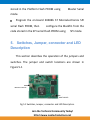
DSP/DSC BOARDS
Hardware User Manual for BF532
Audio Development Board
Contents
1. Introduction .................................................................................. 5
1.1 Technical or Customer Support ............................................... 5
1.2 Packages .................................................................................. 6
2. Introduction and Overview ........................................................... 6
2.2 The Board Features: .................................................................. 9
3. ADSP-BF532 Audio Development Board Hardware Reference ... 11
3.1 System Architecture ................................................................ 11
3.2 Overview ................................................................................. 11
3.3 System Architecture and Peripherals ..................................... 12
3.4 Power connector and Power supply unit ................................ 13
3.5 Push-Button Switches Locations and Labels ......................... 14
3.6 Programmable Flags................................................................ 16
3.7 Programmable LEDs ................................................................ 17
3.8 Clock Sources .......................................................................... 18
3.9 External Bus Interface Unit ..................................................... 26
3.10 Audio Interface ..................................................................... 27
3.11 Memory Map ........................................................................ 28
3.12 SDRAM Interface ................................................................... 29
3.13 Flash Memory ....................................................................... 32
3.14 SPI FLASH Interfaces.............................................................. 35
Join the Technical Community Today!
http://www.pantechsolutions.net
3.15 SPI EXTERNAL INTERFACE ..................................................... 36
3.16 RS-232 Port Serial Ports ........................................................ 37
3.17 Expansion Interface............................................................... 39
3.18 JTAG Emulation Port ............................................................. 39
3.19 Parallel Peripheral Interface ................................................. 42
3.20 Serial Ports (Sports)............................................................... 43
3.21 DMA Controller ..................................................................... 45
3.22 Timers ................................................................................... 46
3.23 General- Purpose I/O Port..................................................... 47
4. Audio Interface ........................................................................... 49
4.1 FEATURES OF AD1836A........................................................... 49
4.2 Connecting AD1836A to BF532 Processor ............................. 52
4.3 Understanding the Serial Port................................................ 56
4.4 Blackfin Configuration Options ............................................... 60
5. Switches, Jumper, connector and LED Description ..................... 61
5.3 Jumper Settings ..................................................................... 62
5.4 BOOTING SETTINGS ............................................................... 62
5.3 Programming Mode ................................................................ 67
5.5 General Mode ........................................................................ 68
5.6 JTAG Connector (J10) ............................................................. 69
5.7 SPI_SLT Select jumper (J13) ................................................... 71
5.8 Timer setting jumper (J8) ....................................................... 71
5.9 Audio configuration switch (SW5) ......................................... 72
5.9 SPI CONNECTOR (J9) ............................................................... 73
5.10 SPORT1 Connector (J7) ......................................................... 73
Join the Technical Community Today!
http://www.pantechsolutions.net
5.11 Connector (J16) ..................................................................... 73
5.12 Memory connector (J15) ....................................................... 73
5.13 Reset Push Button (SW4) ...................................................... 74
5.14 Power LED (D1) ..................................................................... 75
5.15 User LED s (D2–5) .................................................................. 75
5.16 Push Button Enable Switch ................................................... 75
5.17 Board Layout ......................................................................... 78
Join the Technical Community Today!
http://www.pantechsolutions.net
1. Introduction
BF532 Audio Development provides an exclusive generalpurpose development board for initial evaluation of BF532
Processor Audio capabilities in addition to providing platform
for evaluating the BF532 Basic peripherals like EBIU, Timers,
Programmable flags and SPI. The Board has AD1836A audio
codec which is a high performance, single-chip codec that
provides three stereo DACs and two stereo ADCs and 6 Input
RCA jacks and 6 Output RCA jacks for Audio In and Audio
Out.
1.1 Technical or Customer Support
Post your questions:
Pantech forum:
www.pantechsolutions.net/forum
Web site:
www.pantechsolutions.net
Join the Technical Community Today!
http://www.pantechsolutions.net
1.2 Packages
Blackfin532 Audio development Board
5V DC Adaptor
RS232 Serial Cable
10-pin FRC cable
RCA Cables (Audio Connectors)
SPI Programmer (Optional)
Printed USER Manual
CD Contains
o
Example Codes
o
Required Software and Utilities
o
USER and Processor Manuals.
2. Introduction and Overview
Thank you for purchasing the ADSP-BF532 Audio
Development Board, Pantech solutions evaluation system for
Blackfin processors. Blackfin processors support a media
Join the Technical Community Today!
http://www.pantechsolutions.net
instruction
set
computing
(MISC)
architecture.
This
architecture is the natural merging of RISC, media functions,
and digital signal processing (DSP) characteristics. Blackfin
processors deliver signal processing performance in a
microprocessor-like environment. The development board is
designed to be used in conjunction with the VisualDSP++
development environment to test the capabilities of the
ADSP-BF532
Blackfin
processors.
The
VisualDSP++
development environment gives you the ability to perform
advanced application code development and debug, such as:
Create,
compile,
assemble,
and
link
application
programs written in C++, C and ADSP-BF532 assembly
Load, run, step, halt, and set breakpoints in application
program
Use breakpoints to view registers and memory. Quickly
add and remove, and enable and disable breakpoints
VisualDSP++ Kernel (VDK) support
Join the Technical Community Today!
http://www.pantechsolutions.net
Plot values from processor memory. Choose from
multiple
plot
styles,
data
processing
options,
and
presentation options.
Access to the ADSP-BF532 processor from a personal
computer (PC) is achieved through a booting mode
configuration or an optional JTAG emulator. The booting
mode configuration gives access to the ADSP-BF532
processor and the development board peripherals. JTAG
emulators offer faster communication between the host PC
and target hardware.
To learn more about Pantech Solutions kits and development
tools, go to
http://www.pantechsolutions.net/.
ADSP-BF532
Audio
Development
Board
provides
example programs to demonstrate the capabilities of the
Development board.
Join the Technical Community Today!
http://www.pantechsolutions.net
2.2 The Board Features:
Analog Devices ADSP-BF532 processor.
Performance up to 400 MHz
176-pin Lead-LQFP package
Two 16-bit MACs, two 40-bit ALUs, four 8-bit Video
ALUs, 40-bit shifter
Synchronous
Dynamic
Random
Access
Memory
(SDRAM).
MT48LC8M16A2 - 16 MB (8M x 16 bits)
Flash memories.
M29W160EB- 1 MB (512K x 16)
Audio interface
AD1836A – 96 kHz audio codec
6 input RCA phono jacks (2 channels)
6 output RCA phono jacks (3 channels)
Universal asynchronous receiver/transmitter (UART).
ADM3202/MAX3232 RS-232 line driver/receiver
Join the Technical Community Today!
http://www.pantechsolutions.net
DB9 Female connector
LEDs.
1 power (Red)
4 general purpose (Red)
Push buttons.
3 push buttons with debounce logic: 1 reset, 2
programmable flags.
Expansion Interface.
PPI, SPI, EBIU, Timers2-0, UART, programmable flags,
SPORT0, SPORT1.
Other features.
JTAG ICE 14-pin header
The ADSP-BF532 Audio Development Board has a flash
memory with a total of 1 MB of memory. The flash memory
can be used to store user-specific boot code, allowing the
board to run as a stand-alone unit. The board also has 16 MB
of SDRAM, which can be used by the user at runtime. SPORTs
interface with the AD1836AAS audio codec to aid
Join the Technical Community Today!
http://www.pantechsolutions.net
development of audio signal processing applications. SPORT0
is communicating with the Audio codec and then SPORT1 is
connected to the connector for communication with other
serial devices from external.
3. ADSP-BF532 Audio Development Board
Hardware Reference
3.1 System Architecture
This section describes the processor’s configuration on
ADSP-532 audio development board. This ADSP-BF532 audio
development board has been designed to demonstrate the
capabilities of the ADSP-BF532 Blackfin processor. The
processor has an IO voltage of 3.3V. The core voltage of 1.2V
is derived from the 5V DC wall mount supply. The core clock
rate can be set up on the fly by the processor.
3.2 Overview
The ADSP-BF532 Audio Development Board includes the
Join the Technical Community Today!
http://www.pantechsolutions.net
following components and functional specification. As shown
in figure3-1:
JTAG CONNECTOR
MT48LC8M16A2
(SDRAM)
AUDIO CODEC
AD1836AAS
EXPANSION
HEADER
RS-232 SERIAL
PORT
Flash1 MB (512K x
16)
ADSP- BF532
Processor
27 MHz
OSCILLATOR
SPI FLASH (2048
Kilobits) AT25F2048
RESET
3.3V REGULATOR
1.2V REGULATOR
5 VDC, 2A SUPPLY
100-240V AC INPUT
50-60 Hz
Figure3.1: Blackfin Audio development Board Block Diagram
3.3 System Architecture and Peripherals
Default Configuration
To connect the Audio development board:
Join the Technical Community Today!
http://www.pantechsolutions.net
1. Plug the provided power supply into J2 on the Audio
development board. Visually verify that the red power LED
(D1) is on.
SPI
BOOT MODES
DIP SWITCHES
5V DC IP
27 MHz
CRYSTAL
ADC’S
AUDIO
IN
D1
GPIO
AUDIO
OUT
UART
LEDs
SPORT1
BUTTONS
PUSH
CODEC
AUDIO
JTAG
DAC’S
CONNECTOR
Fig 3.2: Blackfin audio development board connections
3.4 Power connector and Power supply unit
The audio development board is received the 5V Dc power
from the wall mount power supply. The Core Voltage is
provided the 1.2V Dc by LD1117 a low drop voltage regulator
able to provide an output current of up to 800mA .The IO
Join the Technical Community Today!
http://www.pantechsolutions.net
Voltage is provided the 3.3V Dc by ADP3339 which is a
member of the ADP33xx family of precision low dropout
voltage regulators. There is RED Power LED D1, which
indicated the Board Power is ON as shown in fig 3.3.
5V INPUT DC
3.3V REGULATOR
27MHz CRYSTAL
1.2V REGULATOR
Fig 3.3 Power connector and Power supply unit
3.5 Push-Button Switches Locations and Labels
The ADSP-BF532 Audio Development Board has three
switches. Two Switches (SW1, SW3) are used for general
purpose and another one is used for reset (SW4). The
general purpose
switches are located in the lower left
corner of the board and are labeled SW1 and SW3 as shown
in fig3.4. Switch SW1is the left-most switch, and SW3 is the
Join the Technical Community Today!
http://www.pantechsolutions.net
right-most switch. The reset switch is located in the upper
left corner of the board and is labeled SW4.
OUTPUT LED’S
PUSH BUTTONS
Fig 3.4 Push-Button Switches
Pressing a push button connects the associated BF532 pin to
3.3V, as shown in Figure 3.5. Use an internal pull-down
resistor within the FPGA pin to generate a logic Low when
the
Button is not pressed. There is no active debouncing circuitry
on the push button.
3V3
R86
10K
SW1
R88
F1
100
AGND
SW PUSHBUTTON-SPST
C106
1UF
AGND
Figure 3.5 Push-Button Switches Require an Internal Pull-Down Resistor
Join the Technical Community Today!
http://www.pantechsolutions.net
3.6 Programmable Flags
The processor has 15 programmable flag pins (PFs). The
pins are multi-functional and depend on the processor setup.
Following table is a summary of the programmable flag pins
are used on the Audio Development Board for switches and
LEDs. Two push buttons, SW1 and SW3 are provided for
general-purpose user input. The buttons connect to the
processor’s programmable flag pins PF7, PF6 The push
buttons are active “LOW” and, when pressed, send a Low (0)
to the processor. The programmable flag signals and their
corresponding switches are shown in fig3.2.
Programmable Flag Switches
Table 3.1 Programmable Flag Switches
Processor
Programmable
Flag Pin
PF6
Push
Button
Reference Designator
PF7
SW1
SW3
Join the Technical Community Today!
http://www.pantechsolutions.net
3.7 Programmable LEDs
Locations and Labels
The Bf 532 board has four individual surface-mount LEDs
located above the Push Button switches as shown in
Figure3.6. The LEDs are labeled D5 through D2. D5 is the leftmost LED, D2 the right-most LED.
CODEC CLK
12.288MHz
OUTPUT LED’S
PUSH BUTTONS
Figure 3.6 Programmable LED
Operation
Each LED has one side connected to ground and the other
side connected to a pin on the Bf 532 device via a 180E
current limiting resistor. To light an individual LED, drive the
associated Bf532 control signal High. Four LEDs connect to
Join the Technical Community Today!
http://www.pantechsolutions.net
four programmable flags of the processor (U12). The LEDs
are active high while the programmable flags act as a output
i.e. the output value is one
Table 4.2 Programmable Led’s
LED
Reference
Processor
Designator
Programmable Flag
D2
PF12
D3
PF9
D4
PF10
D5
PF11
3.8 Clock Sources
Overview
The Blackfin Audio Development board has different clock
input sources which is shown in fig3.7.
The board includes an on-board 27 MHz clock oscillator
for drive the Blackfin processor.
The board includes an on-board 12.288 MHz clock
oscillator for driving the Audio codec.
Join the Technical Community Today!
http://www.pantechsolutions.net
A 2-pin Cylindrical oscillator of Frequency 32.768Mhz for
RTC
27 MHz ON
BOARD CLK
RTC
BF 532
OUTPUT LED’S
AUDIO CODEC
CLK 12.288 MHz
Figure 3.7. Clock Sources
CLOCK SIGNALS
The ADSP-BF531/ADSP-BF532/ADSP-BF533 processor can be
clocked by an external crystal, a sine wave input, or a
buffered, shaped clock derived from an external clock
oscillator. If an external clock is used, it should be a TTL
compatible signal and must not be halted, changed, or
operated below the specified frequency during normal
operation. This signal is connected to the processor’s CLKIN
pin. When an external clock is used, the XTAL pin must be
Join the Technical Community Today!
http://www.pantechsolutions.net
left unconnected. In the Board we are using an External 27
MHz Crystal Oscillator as the main clocking source.
Alternatively, because the ADSP-BF531/ADSP-BF532/ ADSPBF533 processor includes an on-chip oscillator circuit, an
external crystal may be used. For fundamental frequency
operation, use the circuit shown in Fig3.8.
Figure3.8: External Crystal Connections
A parallel-resonant, fundamental frequency, microprocessorgrade crystal is connected across the CLKIN and XTAL pins.
The on-chip resistance between CLKIN and the XTAL pin is in
the 500 kΩ range. Further parallel resistors are typically not
Join the Technical Community Today!
http://www.pantechsolutions.net
recommended. The two capacitors and the series resistor
shown in Figure3. 8 fines tune the phase and amplitude of
the sine frequency. The capacitor and resistor values shown
in Figure3.8 are typical values only. The capacitor values are
dependent upon the crystal manufacturer's load capacitance
recommendations and the physical PCB layout.
The resistor value depends on the drive level specified by the
crystal manufacturer. System designs should verify the
customized values based on careful investigation on multiple
devices over the allowed temperature range. A thirdovertone crystal can be used at frequencies above 25 MHz.
The circuit is then modified to ensure crystal operation only
at the third overtone, by adding a tuned inductor circuit as
shown in above fig3.9. in the following Figure, the core clock
(CCLK) and system peripheral clock (SCLK) are derived from
the input clock (CLKIN) signal. An on-chip PLL is capable of
multiplying the CLKIN signal by a user programmable 0.5× to
64× multiplication factor (bounded by specified minimum
Join the Technical Community Today!
http://www.pantechsolutions.net
and maximum VCO frequencies). The default multiplier is
10×, but it can be modified by a software instruction
sequence. On-the-fly frequency changes can be effected by
simply writing to the PLL_DIV register.
Figure3.9: Frequency Modification Methods
All on-chip peripherals are clocked by the system clock
(SCLK). The system clock frequency is programmable by
means of the SSEL3–0 bits of the PLL_DIV register. The values
programmed into the SSEL fields define a divide ratio
between the PLL output (VCO) and the system clock. SCLK
divider values are 1 through 15.
Join the Technical Community Today!
http://www.pantechsolutions.net
Example System Clock Ratios
The maximum frequency of the system clock is fSCLK. The
divisor ratio must be chosen to limit the system clock
frequency to its maximum of fSCLK. The SSEL value can be
changed dynamically without any PLL lock latencies by
writing the appropriate values to the PLL divisor register
(PLL_DIV). When the SSEL value is changed, it will affect all
the peripherals that derive their clock signals from the SCLK
signal. The core clock (CCLK) frequency can also be
dynamically changed by means of the CSEL1–0 bits of the
PLL_DIV register. Supported CCLK divider ratios are 1, 2, 4,
and 8, as shown in Table 3.2. This programmable core clock
capability is useful for fast core frequency modifications.
Join the Technical Community Today!
http://www.pantechsolutions.net
Core Clock Ratios
Table 3.2 Core Clock Ratios
Real Time Clock (RTC)
The processor real-time clock (RTC) provides a robust set of
digital watch features, including current time, stopwatch,
and alarm. The RTC is clocked by a 32.768 kHz crystal
external to the ADSP-BF532 processor. The RTC peripheral
has dedicated power supply pins so that it can remain
powered up and clocked even when the rest of the processor
is in a low power state. The RTC provides several
programmable interrupt options, including interrupt per
second, minute, hour, or day clock ticks, interrupt on
programmable stopwatch countdown, or interrupt at a
programmed alarm time.
Join the Technical Community Today!
http://www.pantechsolutions.net
Like other peripherals, the RTC can wake up the processor
from sleep mode upon generation of any RTC wakeup event.
Additionally, an RTC wakeup event can wake up the
processor from deep sleep mode, and wake up the on-chip
internal voltage regulator from a powered-down state.
Connect RTC pins RTXI and RTXO with external components
as shown in Figure3.10.
Figure3.10: External Components for RTC
Suggested Components:
x1= Ecliptekec38j (through-hole package)or
Epson mc405 12 pf load (surface-mount package)
c1 = 22pf
c2 = 22pf
Join the Technical Community Today!
http://www.pantechsolutions.net
r1 =10mω
Note:
c1 and c2 are specific to crystal specified for x1., Contact
crystal manufacturer for details. c1and c2, Specifications
assume board trace capacitance of 3pf.
3.9 External Bus Interface Unit
External memory is accessed via the external bus interface
unit (EBIU). This 16-bit interface provides a glueless
connection to a bank of synchronous DRAM (SDRAM) as well
as up to four banks of asynchronous memory devices
including flash, EPROM, ROM, SRAM, and memory mapped
I/O devices.
The PC133-compliant SDRAM controller can be programmed
to interface to up to 128M bytes of SDRAM. The SDRAM
controller allows one row to be open for each internal
SDRAM bank, for up to four internal SDRAM banks,
improving overall system performance.
Join the Technical Community Today!
http://www.pantechsolutions.net
The asynchronous memory controller can be programmed to
control up to four banks of devices with very flexible timing
parameters for a wide variety of devices. Each bank occupies
a1M byte segment regardless of the size of the devices used,
so that these banks will only be contiguous if each is fully
populated with 1M byte of memory.
3.10 Audio Interface
The AD1836 audio codec provides three channels of stereo
audio output and two channels of
Stereo multichannel 96 kHz input. The SPORT0 interface of
the processor links with the stereo audio data input and
output pins of the AD1836 codec. The processor is capable of
transferring data to the audio codec in time-division
multiplexed (TDM) or two-wire interface (TWI) mode. The
TWI mode allows the codec to operate at a 96 kHz sample
rate but limits the output channels to two. The TDM mode
can operate at a maximum of 48 kHz sample rate but allows
Join the Technical Community Today!
http://www.pantechsolutions.net
simultaneous use of all input and output channels. When
using TWI mode, the TSCLK0 and RSCLK0 pins, as well as the
TFS0 and RFS0 pins of the processor, must be tied together
external to the processor.
3.11 Memory Map
External memory is accessed via the external bus interface
unit (EBIU). This 16-bit interface provides a glueless
connection to a bank of synchronous DRAM (SDRAM) as well
as up to four banks of asynchronous memory devices
including flash, EPROM, ROM, SRAM, and memory mapped
I/O devices. The PC133-compliant SDRAM controller can be
programmed to interface to up to 128M bytes of SDRAM. The
SDRAM controller allows one row to be open for each
internal SDRAM bank, for up to four internal SDRAM banks,
improving overall system performance. The Asynchronous
memory controller (AMC) can be programmed to control up
to four banks of devices with very flexible timing parameters
for a wide variety of devices. Each bank occupies a 1M byte
segment regardless of the size of the devices used, so that
these banks will only be contiguous if each is fully populated
Join the Technical Community Today!
http://www.pantechsolutions.net
with 1M byte of memory. The ADSP-BF532 processor has
internal SRAM that can be used for instruction or data
storage. The configuration of internal SRAM is detailed in the
ADSP-BF532 Processor Hardware Reference. The ADSPBF532 Audio development board includes two types of
external memory, SDRAM and flash memory. The size of the
SDRAM is 16 MB (8M x 16 bits). The processor’s memory
select pin ~SMS0 is configured for the SDRAM. The size of the
Flash memory is 1MB (1Mx 8). The processor’s memory
select pins ~AMS0, ~AMS1, and ~AMS2 is configured for flash
memory.
3.12 SDRAM Interface
The three SDRAM control registers must be initialized
properly in order to use the MT48LC8M16A2 - 16 MB (8M x
16 bits) SDRAM memory. When we are using the Audio
development with emulator the SDRAM registers are set
automatically to the values listed in Table 3.4 based on the
values we have given in the XML files. To disable this feature,
Join the Technical Community Today!
http://www.pantechsolutions.net
clear the Use XML reset values check box on the Target
Options dialog box, this is accessible through the Settings
pull-down menu. The values are derived for maximum
flexibility and work for a system clock frequency between 54
MHz and 133 MHz For more information about the Target
Options dialog box, see the online Help. Automatic
configuration of SDRAM is not optimized for any SCLK
frequency. Table 3.3 shows the optimized configuration for
the SDRAM registers using a 118.8 MHz, 126 MHz, and 133
MHz SCLK. Only the EBIU_SDRRC register needs to be
modified in the user code to achieve maximum performance.
Table 3-3. Development Board Memory Map
Join the Technical Community Today!
http://www.pantechsolutions.net
Start Address
External
Memory
Internal
Memory
Content
0x0000
0000
0x2000
0000
0x2010
0000
End
Address
0x07FF
FFFF
0x200F
FFFF
0x201F
FFFF
0x2020
0000
0x202F
FFFF
ASYNC Memory bank 2
0xFF800000
0xFF80
3FFF
0xFF80
7FFF
0xFF90
3FFF
0xFF90
7FFF
Data bank A SRAM 16 KB
Instruction SRAM 64 KB
0xFFA1
0000
0xFFA0
FFFF
0xFFA1
3FFF
0xFFB0
0000
0xFFB0
0FFF
Scratch Pad SRAM 4 KB
0xFFC0
0000
0xFFDF
FFFF
System MMRs 2MB
0xFFE0
0000
0xFFFF FFFF
Core MMRs 2MB
0xFF804000
0xFF900000
0xFF904000
0xFFA00000
Internal
Memory
All other locations
SDRAM bank 0 (SDRAM).
ASYNC memory bank 0
ASYNC memory bank 1
Data bank A SRAM /CACHE
16 DB
Data bank B SRAM 16 KB
Data bank B SRAM /CACHE
16 KB
Instruction SRAM /CACHE
16DB
Reserved
Join the Technical Community Today!
http://www.pantechsolutions.net
Table 3-4. SDRAM Optimum Setting
Register
SCLK = 118.8 MHz
(CCLK = 128 MHz)
0x0091 998D
EBIU_SDGCTL
EBIU_SDBCTL
0x0000 0013
ADSP-BF533 EZ-KIT Lite
revision 1.5 and below
0x0000 0025
ADSP-BF533 EZ-KIT Lite
revision 1.6 and above
EBIU_SDRRC
0x0000 0397
An example program is included in the Audio board
installation directory to demonstrate how to set up the
SDRAM interface.
3.13 Flash Memory
The following sections describe how to use the memory pins,
as well as how to configure the flash memory devices.
Example code is provided in the Audio board installation
directory to demonstrate how to program the flash memory
Join the Technical Community Today!
http://www.pantechsolutions.net
as well as to demonstrate the functionality of the generalpurpose IO pins.
Flash Memory Map
The Flash Chip used in the board is M29W160EB 16 Mbits
(2Mb x8 or 1Mb x16, Boot Block) 3V Supply Flash Memory
from STMicroelectronics. Access to each segment can be 8bit or 16-bit. The processor’s ~AMS0, ~AMS1, and ~AMS2
memory select pin are used for that purpose. Asynchronous
memory bank 0 is always enabled after a hard reset, while
banks 1 and 2 need to be enabled by software. Table 3-5, 3.6
provides an example on asynchronous memory configuration
registers. The flash chip is interfaced to the first memory
bank which is selected by ~AMS0. So, this bank will be
enabled always enabled at the reset.
Join the Technical Community Today!
http://www.pantechsolutions.net
Table 3-5. Asynchronous Memory Control Registers Settings Example
Register
Value
Function
EBIU_AMBCTL0
0x7BB07BB0
Timing control for banks 1 and 0
EBIU_AMBCTL1 bits 150
EBIU_AMGCTL bits 3-0
0x7BB0
Timing control for bank 2 (bank 3 is
not used)
Enable all banks
0xF
Table 3-6. Flash Memory Map
Start Address End Address
Content
0x2000 0000
Asynchronous bank0
0x200F FFFF
(1MB)
0x2010 0000
0x201F FFFF
Asynchronous bank1
(1MB)
0x2020 0000
0x202F FFFF
Asynchronous bank2
(1MB)
0x2030 0000
0x203F FFFF
Asynchronous bank3
(1MB)
All other locations
Reserved
Join the Technical Community Today!
http://www.pantechsolutions.net
3.14 SPI FLASH Interfaces
The
AT25F2048
provides
2,097,152
bits
of
serial
reprogrammable Flash memory organized as 262,144 words
of 8 bits each. The device is optimized for use in many
Industrial and commercial applications where low-power and
low-voltage operation are essential. The AT25F2048 is
available in a space-saving 8-lead JEDEC SOIC and Ultra Thin
SAP package.
The ADSP-BF532 processor has an SPI-compatible port that
enables the processor to communicate with multiple SPIcompatible devices. The baud rate and clock phase/polarities
for the SPI port are programmable, and it has an integrated
DMA controller, configurable to support transmits or receives
data streams. The SPI DMA controller can only service
unidirectional accesses at any given time.
The SPI port clock rate is calculated as:
Join the Technical Community Today!
http://www.pantechsolutions.net
FSCLK
SPI Clock Rate = ----------------------------------2 × SPI_BAUD
Where the 16-bit SPI_BAUD register contains a value of 2 to
65,535.
Pin Configurations
Table 3-6. Pin Configurations
Pin Name
Function
CS
Chip Select
SCK
Serial Data Clock
SI
Serial Data Input
SO
Serial Data Output
GND
Ground
VCC
Power Supply
WP
Write Protect
HOLD
Suspends Serial Input
3.15 SPI EXTERNAL INTERFACE
The Board contains an external SPI Connector (J13) for
Join the Technical Community Today!
http://www.pantechsolutions.net
Programming the Onboard SPI Flash by external means. The
AT89C51RD2 SPI Flash Programmer has to be purchased
separately for Programming. The power for the SPI
Programmer also provided by the audio development board
by using this external SPI connector
3.16 RS-232 Port Serial Ports
The ADSP-BF532 processor provides a full-duplex universal
asynchronous receiver/transmitter (UART) port, which is fully
compatible with PC-standard UARTs. The UART port provides
a simplified UART interface to other peripherals or hosts,
supporting
full-duplex,
DMA-supported,
asynchronous
transfers of serial data. The UART port includes support for 5
data bits to 8 data bits, 1 stop bit or 2 stop bits, and none,
even, or odd parity. The UART port supports two modes of
operation.
Join the Technical Community Today!
http://www.pantechsolutions.net
PIO (programmed I/O) – The processor sends or receives data
by writing or reading I/O-mapped UART registers. The data is
double-buffered on both transmit and receive. DMA (direct
memory access) – The DMA controller transfers both
transmit and receive data. This reduces the number and
frequency of interrupts required to transfer data to and from
memory. The UART has two dedicated DMA channels, one
for transmit and one for receive. These DMA channels have
lower default priority than most DMA channels because of
their relatively low service rates.
Rs-232 communication enables point-to-point
data transfer. It is commonly used in data Acquisition
applications, for the transfer of data between the BF-532
Processor and a PC.
The voltage levels of a BF-532 Processor and PC
are not directly compatible with those of RS-232, a level
transition buffer such as MAX232 be used.
Join the Technical Community Today!
http://www.pantechsolutions.net
Rs-232(P1) is a female connector. The 2nd and
3rd pin of P1 is receiving and transmitting pin for transferring
the data as shown in fig 3.11.
DB9 CONNECTOR
MAX3232
Figure 3.11 UART INTERFACE
3.17 Expansion Interface
The expansion interface consists of SPORT1 Connector, 1
Timer Connector,1 External SPI interface Connector For
Programming the Onboard SPI flash(AT25F2048),Boot Mode
Connectors, other connectors for Write Protection and a
14pin JTAG header which s used for in-circuit Emulation.
3.18 JTAG Emulation Port
Join the Technical Community Today!
http://www.pantechsolutions.net
The JTAG emulation port allows an emulator to access
the processor’s internal and external memory through a 14pin interface. To learn more about available emulators,
contact Analog Devices (see “Product Information”).
System Peripherals
Parallel peripheral interface PPI/GPIO,
full duplex synchronous serial ports,
supporting eight stereo I2S channels
SPI-compatible port
Three 32-bit timer/counters with PWM support
Real-time clock and watchdog timer
32-bit core timer
Up to 16 general-purpose I/O pins (GPIO)
UART with support for IrDA
Event handler
Debug/JTAG interface
Join the Technical Community Today!
http://www.pantechsolutions.net
On-chip PLL capable of 0.5 * to 64 * frequency
multiplication
TheADSP-BF532 processor contain a rich set of peripherals
connected to the core via several high bandwidth buses,
providing flexibility in system configuration as well as
excellent overall system performance. The general-purpose
peripherals include functions such as UART, timers with
PWM and pulse measurement capability, general-purpose
I/O pins, a real-time clock, and a watchdog timer. This set of
functions satisfies a wide variety of typical system support
needs and is augmented by the system expansion capabilities
of the part. In addition to these general-purpose peripherals,
the ADSP- ADSP-BF532 processor contain high speed serial
and parallel ports for interfacing to a variety of audio and
modem codec functions; an interrupt controller for flexible
management of interrupts from the on-chip peripherals or
external sources; and power management control functions
to tailor the performance and power characteristics of the
processor and system to many application scenarios.
Join the Technical Community Today!
http://www.pantechsolutions.net
All of the peripherals, except for general-purpose I/O, realtime clock, and timers, are supported by a flexible DMA
structure. There is also a separate memory DMA channel
dedicated to data transfers between the processor’s various
memory spaces, including external SDRAM and
asynchronous memory. Multiple on-chip buses running at up
to 133 MHz provide enough bandwidth to keep the
processor core running along with activity on all of the onchip and external peripherals. The ADSP-BF532 processor
includes an on-chip voltage regulator in support of the
processor’s dynamic power management capability. The
voltage regulator provides a range of core voltage levels
from a single 2.25 V to 3.6 V input. The voltage regulator can
be bypassed at the user’s discretion
3.19 Parallel Peripheral Interface
The processor provides a parallel peripheral interface (PPI)
that can connect directly to parallel A/D and D/A converters,
Video encoders and decoders, and other general-purpose
Join the Technical Community Today!
http://www.pantechsolutions.net
peripherals. The PPI consists of a dedicated input clock pin,
up to three frame synchronization pins, and up to 16 data
pins. The input clock supports parallel data rates up to half
the system clock rate and the synchronization signals can be
configured as either inputs or outputs. The PPI supports a
variety of general-purpose and ITU-R 656 modes of
operation. In general-purpose mode, the PPI provides halfduplex, bidirectional data transfer with up to 16 bits of data.
Up to three frame synchronization signals are also provided.
In ITU-R 656 mode, the PPI provides half-duplex bidirectional
transfer of 8- or 10-bit Audio data.
3.20 Serial Ports (Sports)
The ADSP-BF532 processor incorporates two dual-channel
synchronous serial ports (SPORT0 and SPORT1) for serial and
multiprocessor communications.
The SPORTs support the following features
2
I S capable operation.
Join the Technical Community Today!
http://www.pantechsolutions.net
Bidirectional operation – Each SPORT has two sets of
independent transmit and receive pins, enabling eight
2
channels of I S stereo audio.
Buffered (8-deep) transmit and receive ports – Each port
has a data register for transferring data words to and from
other processor components and shift registers for shifting
data in and out of the data registers.
Clocking – Each transmit and receive port can either use
an external serial clock or generate its own, in frequencies
ranging from (fSCLK/131,070) Hz to (fSCLK/2) Hz.
Word length – Each SPORT supports serial data words
from 3 bits to 32 bits in length, transferred most-significantbit first or least-significant-bit first.
Framing – Each transmit and receive port can run with or
without frame sync signals for each data word. Frame sync
signals can be generated internally or externally, active high
or low, and with either of two pulse widths and early or late
frame sync.
Join the Technical Community Today!
http://www.pantechsolutions.net
Companding in hardware – Each SPORT can perform Alaw or μ-law companding according to ITU recommendation
G.711. Companding can be selected on the Transmit and/or
receive channel of the SPORT without additional latencies.
DMA operations with single-cycle overhead – Each
SPORT can automatically receive and transmit multiple
buffers of memory data. The processor can link or chain
sequences of DMA transfers between a SPORT and memory.
Interrupts – Each transmit and receive port generates an
interrupt upon completing the transfer of a data-word or
after transferring an entire data buffer or buffers through
DMA.
Multichannel capability – Each SPORT supports 128
channels out of a 1,024-channel window and is compatible
with the H.100, H.110, MVIP-90, and HMVIP standards.
3.21 DMA Controller
Join the Technical Community Today!
http://www.pantechsolutions.net
The ADSP-BF532 processor has multiple, independent DMA
channels that support automated data transfers with
minimal overhead for the processor core. DMA transfers can
occur between the processor’s internal memories and any of
its DMA-capable peripherals. Additionally, DMA transfers can
be accomplished between any of the DMA-capable
peripherals and external devices connected to the external
memory interfaces, including the SDRAM controller and the
asynchronous memory controller. DMA-capable peripherals
include the SPORTs, SPI port, UART, and PPI. Each individual
DMA-capable peripheral has at least one dedicated DMA
channel.
3.22 Timers
There are four general-purpose programmable timer units in
the ADSP-BF532processor. Three timers have an external pin
that can be configured either as a pulse-width modulator
Join the Technical Community Today!
http://www.pantechsolutions.net
(PWM) or timer output, as an input to clock the timer, or as a
mechanism for measuring pulse widths and periods of
external events. These timers can be synchronized to an
external clock input to the PF1 pin (TACLK), an external clock
input to the PPI_CLK pin (TMRCLK), or to the internal SCLK.
3.23 General- Purpose I/O Port
The ADSP-BF532 processor has 16 bidirectional, generalpurpose I/O pins on Port F (PF15–0). Each general-purpose
I/O pin can be individually controlled by manipulation of the
GPIO control, status and interrupt registers:
GPIO direction control register – Specifies the direction
of each individual PFx pin as input or output.
GPIO control and status registers – The ADSP-BF532
processor employs a “write one to modify” mechanism that
allows any combination of individual GPIO pins to be
modified in a single instruction, without affecting the level of
Join the Technical Community Today!
http://www.pantechsolutions.net
any other GPIO pins. Four control registers are provided. One
register is written in order to set GPIO pin values, one
register is written in order to clear GPIO pin values, one
register is written in order to toggle GPIO pin values, and one
register is written in order to specify GPIO pin values.
Reading the GPIO status register allows software to
interrogate the sense of the GPIO pin.
GPIO interrupt mask registers – The two GPIO interrupt
mask registers allow each individual PFx pin to function as an
interrupt to the processor. Similar to the two GPIO control
registers that are used to set and clear individual GPIO pin
values, one GPIO interrupt mask register sets bits to enable
interrupt function, and the other GPIO interrupt mask
register clears bits to disable interrupt function. PFx pins
defined as inputs can be configured to generate hard ware
interrupts, while output PFx pins can be triggered by
software interrupts.
Join the Technical Community Today!
http://www.pantechsolutions.net
GPIO interrupt sensitivity registers – The two GPIO
interrupt sensitivity registers specify whether individual PFx
pins are level- or edge-sensitive and specify—if edgesensitive—whether just the rising edge or both the rising and
falling edges of the signal are significant. One register selects
the type of sensitivity, and one register selects which edges
are significant for edge-sensitivity
4.
Audio Interface
4.1 FEATURES OF AD1836A
5 V Multichannel audio system
Accepts 16-/18-/20-/24-bit data
Supports 24-bit and 96 kHz sample rate
Multibit Σ-Δ modulators with data directed scrambling
Differential output for optimum performance
ADCs: –92 dB THD + N, 105 dB SNR and dynamic range
Join the Technical Community Today!
http://www.pantechsolutions.net
DACs: –95 dB THD + N, 108 dB SNR and dynamic range
On-chip volume control with "auto-ramp" function
Programmable gain amplifier for ADC input
Hardware and software controllable click less mute
Digital de-emphasis processing
Supports 256 × fS, 512 × fS, or 768 × fS master clock
Power-down mode plus soft power-down mode
Flexible serial data port with right justified, left justified,
I2S compatible, and DSP serial port modes
TDM interface mode supports 8 in/8 out using a single
SHARC® SPORT
52-lead MQFP (PQFP) plastic package
The AD1836A is a high performance, single-chip codec that
provides three stereo DACs and two stereo ADCs using ADI’s
patented multibit Σ-Δ architecture. An SPI® port is included,
allowing a microcontroller to adjust volume and many other
Join the Technical Community Today!
http://www.pantechsolutions.net
parameters. The AD1836A operates from a 5 V dc supply,
with provision for a separate output supply to interface with
low voltage external circuitry. The AD1836A is available in a
52-lead MQFP (PQFP) package. The AD1836AAS audio codec
provides three channels of stereo audio output and two
channels of multichannel 96 kHz input. The SPORT0 interface
of the processor links with the stereo audio data input and
output pins of the AD1836AAS codec. The processor is
capable of transferring data to the audio codec in timedivision multiplexed (TDM) or two-wire interface (TWI)
mode. The TWI mode allows the codec to operate at a 96
kHz sample rate but limits the output channels to two. The
TDM mode can operate at a maximum of 48 kHz sample rate
but allows simultaneous use of all input and output channels.
When using TWI mode, the TSCLK0 and RSCLK0 pins, as well
as the TFS0 and RFS0 pins of the processor, must be tied
together external to the processor. This is accomplished with
the SW2 DIP switch
Join the Technical Community Today!
http://www.pantechsolutions.net
4.2 Connecting AD1836A to BF532 Processor
The BF533 processor has two serial ports: SPORT0 and
SPORT1. Each serial port provides synchronous serial data
transfer and supports full-duplex communications (i.e.,
simultaneous data transfer in both directions). Figure 4.1
shows the connection between the AD1836A CODEC and the
BF533 processor. SPORT0 receives serial data on its primary
(DR0PRI) and secondary (DR0SEC) inputs and transmits serial
data on its primary (DT0PRI) and secondary (DT0SEC) outputs
simultaneously. SPORT1 can provide another two input and
two output channels. Together, these two SPORTs support
four input (stereo) channels and four output (stereo)
channels. Note that transmit data are synchronous to the
transmit clock (TCLKx) and receive data are synchronous to
the receive clock (RCLKx), where x = 0 or 1 represents the
selected SPORT.
Join the Technical Community Today!
http://www.pantechsolutions.net
ADSP-BF533
AD1836 CODEC
TCLK0
TFS0
RCLK0
RFSO
DBCLK
DLRCLK
ABCLK
ALRCLK
DT0PR1
DTOPR1
DSDATA1
ASDATA1
DT0SEC
DR0SEC
DSDATA2
ASDATA2
SPISS
SPICLK
MOSI
MISO
CLATCH
CCLK
CDATA
COUT
SPORT0
SPI
INTERFACE
4.1 Block diagram for Serial connection between BF533
processor and AD1836A CODEC
Figure 4.1 shows that these serial clocks are input from the
CODEC. In addition, frame synchronization signals for receive
(RFSx) and transmit (TFSx) are provided by the external
device to signal the start of serial data words. A serial
peripheral interface (SPI) port in the BF533 processor is used
to program the internal control registers of the CODEC with
the configuration listed in AD1836A datasheet. The SPI
control port is a four-wire control port consisting of two data
Join the Technical Community Today!
http://www.pantechsolutions.net
ports (MOSI and MISO), one device select pin (SPISS), and a
clock pin (SPICLK). Like SPORT, SPI supports full-duplex
operation. In the connection with the AD1836A. SPI allows
reading of the ADC peak signal levels through the ADC-peak
level data registers. The DAC output level can be
independently programmed with the DAC volume register.
The AD1836A CODEC can operate in the TDM mode. In this
mode, two ADC left channels (L0 and L1) and two right
channels (R0 and R1) occupy slots #1, #2, #5, and #6 of
ASDATA1, respectively, as shown in Figure 4.2. Six DAC
channels within the AD1836A occupy the six time slots of
DSDATA1 as shown in Figure 4.2. A special TDM auxiliary
mode allows two external stereo ADCs and one external
stereo DAC to be interfaced to the AD1836A to form a total
of eight input and eight output transfers. These external
CODECs’ time slots are marked with “AUX.” Each time slot is
32 bits wide and is most signify cant bit (MSB) first. Because
AD1836A has a maximum of 24-bit resolution, the least
Join the Technical Community Today!
http://www.pantechsolutions.net
signify cant 8 bits in the time slot are filled with zeros. By
default, the frequency of the master clock, BCLK, is 32
bits/slot × 8 slot/ frame × 48 frame/s = 12.288 Mbits/s (or
MHz). Therefore, the period of the frame sync, FSTDM, is
20.8 μs (or fs = 48 kHz), and eight input and eight output data
streams can be received and transmitted during this period.
Besides the TDM mode, the data format of the AD1836A
CODEC can also be configured as I2S, right-justify (RJ), leftjustified (LJ), or DSP mode according to
Figure 4.2 TDM timing diagram
Join the Technical Community Today!
http://www.pantechsolutions.net
ADC control register 2 and DAC control register 1, as shown
in Data sheet. By default, the data format for the AD1836A is
the I2S format. The I2S is a three-wire serial bus standard
protocol developed by Philips for transmission of two
channels of pulse code modulation (PCM) digital data. The
I2S protocol is similar to the TDM mode, with only two time
slots for left and right channels.
4.3 Understanding the Serial Port
This section examines the serial port (SPORT) of the BF532
processor. Figure 4.3 shows a block diagram of a single
SPORT. Serial data from the ADC are connected to the
primary receive (DRPRI) pin and secondary receive (DRSEC)
pin and shifted bit by bit into the receive-primary (RX PRI)
shift register and receive secondary (RX SEC) shift register,
respectively. The primary and secondary serial data bits are
synchronized to the receive clock (RCLK), which can be
Join the Technical Community Today!
http://www.pantechsolutions.net
generated from the internal clock generator in the processor
or from an external clock source.
Figure 4.3 SPORT block diagram
The receive frame synchronization signal (RFS) indicates
the start of the serial data. An optional companding
hardware block supports the A-law or μ-law companding
algorithm to reduce the number of bits before storing the
received word in the RX PRI and RX SEC data registers. The
Join the Technical Community Today!
http://www.pantechsolutions.net
primary and secondary data can be stored in the 8 × 16 bits
(or 4 × 32 bits) receive first-in first-out (RX FIFO) in an
interleaved manner. Finally, the data can be retrieved by the
data address generator (DAG).The transmit section of the
SPORT transmits data from the processor to the DAC. Data
from the Blackfin register are written to the 8 × 16 bits (or 4
× 32 bits) transmit first-in first-out (TX FIFO) in an alternating
manner of primary-secondary channel. Again, data from the
TX PRI and TX SEC can be optionally compressed by the
companding hardware and transferred to the TX PRI and TX
SEC shift registers. Finally, the bits in the shift registers are
shifted out to the DAC via the data transmit-primary (DT PRI)
and data transmit-secondary (DT SEC) pins. The transmit
clock (TCLK) synchronizes the transmit data bit, and the
transmit frame synchronization signal (TFS) indicates the
start of transmission. Both RX FIFO and TX FIFO are 16 bits
wide and 8 words deep. These FIFOs are common to both
primary and secondary data arranged in an interleaved
Join the Technical Community Today!
http://www.pantechsolutions.net
manner, with primary first and then secondary. Therefore,
there are four possible data arrangements for the FIFO:
1. When the data length is less than or equal to 16 bits and
only the primary channel is enabled, a total of 8 primary
words can be stored into the FIFO.
2. When the data length is greater than 16 bits and only the
primary channel is enabled, a total of 4 primary words can be
stored into the FIFO.
3. When the data length is less than or equal to 16 bits and
both primary and secondary channels are enabled, a total of
4 primary and 4 secondary words can be stored into the
FIFO.
4. When the data length is greater than 16 bits and both
primary and secondary channels are enabled, a total of 2
primary and 2 secondary words can be stored into the FIFO.
Join the Technical Community Today!
http://www.pantechsolutions.net
The serial port must be configured before transmit or
receive of data. There are two transmit configuration
registers (SPORTx_TCR1 and SPORT_TCR2) per serial port for
setting up the SPORT transmit. Similarly, two registers
(SPORTx_RCR1 and SPORTx_RCR2) per serial port are used
for configuring the receive side. These configuration registers
can only be changed while the SPORT is disabled by setting
TSPEN/RSPEN = 0 (in TCR1 and RCR1 registers).
4.4 Blackfin Configuration Options
The Blackfin Audio Development Board supports a
variety of Blackfin Booting configuration options:
Download the application code directly to the Bf-532 via
JTAG Emulator. SPI serial Flash programming is performed
separately.
Program the on-board M29W160D- 1 MB (512K x 16)
Flash PROM, then
configure the Blackfin from the code
Join the Technical Community Today!
http://www.pantechsolutions.net
stored in the Platform Flash PROM using
Master Serial
mode.
Program the on-board 2048Kb ST Microelectronics SPI
serial Flash PROM, then
configure the Blackfin from the
code stored in the SPI serial Flash PROM using
SPI mode.
5. Switches, Jumper, connector and LED
Description
This section describes the operation of the jumpers and
switches. The jumper and switch locations are shown in
Figure 5-1
400 MHz CRYSTAL
BOOT MODES
Fig 5.1 Switches, Jumper, connector and LED Description.
Join the Technical Community Today!
http://www.pantechsolutions.net
5.3 Jumper Settings
The Utility code is stored in SPI Flash memory using
microcontroller .The purpose of utility code is whatever data
coming from Uart (loader file) receive and send to Flash
memory. At the time jumper should be located in J16 After
receiving the ldr file Press the reset Button. Then change the
Jumper Settings from J16 to J13 As shown in figure5.1. Now
the processor Boot from 1 MB (512K x 16) Flash PROM. More
details please see “software manual’
5.4 BOOTING SETTINGS
Configuration Mode Jumpers
The ADSP-BF531 / ADSP-BF532 /ADSP-BF533 processor
has two mechanisms (listed in Table 5.1 ) for automatically
loading internal L1 instruction memory after a reset. A third
Join the Technical Community Today!
http://www.pantechsolutions.net
mode is provided to execute from external memory,
bypassing the boot sequence.
Booting modes connector (J5, J6)
The ADSP-BF531 /ADSP-BF532 /ADSP-BF533 processor
has two mechanisms (listed in Table) for automatically
loading internal L1 instruction memory after a reset. A third
mode is provided to execute from external memory,
bypassing the boot sequence.
Table 5.1 Booting configurations
Join the Technical Community Today!
http://www.pantechsolutions.net
Jumper settings
J5-BMODE1
J6-BMODE0
Boot
Mode
Description
00
Execute from 16 bit
external memory
01
Boot from 8bit/16
bit flash
10
Boot from serial
master
11
Boot from serial
slave
EEPROM/flash(8/16or 24 bit address
range )
The BMODE pins of the reset configuration register,
sampled during power-on resets and software-initiated
resets, implement the following modes:
Execute from 16-bit external memory – Execution starts
from address 0x2000 0000 with 16-bit packing. The boot
ROM is bypassed in this mode. All configuration settings are
Join the Technical Community Today!
http://www.pantechsolutions.net
set for the slowest device possible (3-cycle hold time; 15cycle R/W access times; 4-cycle setup).
Boot from 8-bit or 16-bit external flash memory – The flash
boot routine located in boot ROM memory space is set up
using asynchronous Memory Bank 0. All configuration
settings are set for the slowest device possible (3-cycle hold
time; 15-cycle R/W access times; 4-cycle setup).
Boot from SPI serial EEPROM/flash (8-, 16-, or 24-bit
addressable,
or
Atmel
AT45DB041,
AT45DB081,
or
AT45DB161) – The SPI uses the PF2 output pin to select a
single SPI EEPROM/flash device, submits a read command
and successive address bytes (0x00) until a valid 8-, 16-, or
24-bit addressable EEPROM/flash device is detected, and
begins clocking data into
the processor at the beginning of
L1 instruction memory.
Boot from SPI serial master – The Blackfin processor
operates in SPI slave mode and is configured to receive the
bytes of the LDR file from an SPI host (master) agent. To hold
Join the Technical Community Today!
http://www.pantechsolutions.net
off the host device from transmitting while the boot ROM is
busy, the Blackfin processor asserts a GPIO pin, called host
wait (HWAIT), to signal the host device not to send any more
bytes until the flag is deasserted. The GPIO pin is chosen by
the user and this information is transferred to the Blackfin
processor via bits[10:5] of the FLAG header in the LDR image.
For each of the boot modes, a 10-byte header is first read
from an external memory device. The header specifies the
number of bytes to be transferred and the memory
destination address. Multiple memory blocks may be loaded
by any boot sequence. Once all blocks are loaded, program
execution commences from the start of L1 instruction SRAM.
In addition, Bit 4 of the reset configuration register can be set
by application code to bypass the normal boot sequence
during a software reset. For this case, the processor jumps
directly to the beginning of L1 instruction memory.
We have two modes ,
Join the Technical Community Today!
http://www.pantechsolutions.net
Programming Mode
General or Normal Mode
5.3 Programming Mode
In Programming Mode
J5, J6 should be connected on No
Connection side (NC) as shown below .This mode will boot
the processor from SPI
J16, WP should have a jumper as shown below,
SSEL (J13) should be configured for BF532 as shown
below
Join the Technical Community Today!
http://www.pantechsolutions.net
MOSI Pin (J12) should HIGH at the RESET for the Booting
from SPI Flash to work properly.
For more information see EE-240
5.5 General Mode
In general mode a jumper must be connected to J5 and J6 as
shown below.
And Reset the kit , Previously whatever are there in the
”Programming Mode” keep all
Join the Technical Community Today!
http://www.pantechsolutions.net
Additionally
just we need to put the JUMPER in J6 or
BMODE1 in “C” side Now the Boot Mode is changed to “01 ”
where it will Boot from 8-bit/16-bit Flash
5.6 JTAG Connector (J10)
All ADI JTAG emulators interface with the DSP using a 14-pin
JTAG emulator header. The header provides a connection
interface for the JTAG emulator pod. The header can also be
used to connect an optional local (embedded on the user
target) boundary scan controller to the DSP when the JTAG
emulator is not attached.
All ADI JTAG emulators use a superset of the IEEE 1149.1
standard to send and receive data from the DSP JTAG
emulation port. JTAG emulators use an additional signal
called EMU~ as a JTAG emulation status flag from the DSP.
This signal is a vendor-specific signal, which is not part of the
IEEE 1149.1 Specification. You must supply this header on
your target to communicate with the JTAG emulator. The
Join the Technical Community Today!
http://www.pantechsolutions.net
JTAG emulator target header interface is a standard dual-row
0.025” male square-post header, employing 0.1” x 0.1”
spacing, with a minimum post length of 0.235”.Pin 3 of the
JTAG emulator cable header is keyed to prevent accidental
insertion of the pod with the target backwards. You should
clip pin 3 on your target board header to allow insertion of
the JTAG emulator cable female header.
When using an emulator with the Audio development board
follows the connection instructions provided with the
emulator .As shown in figure.
GND 1
NO PIN3
BTMS/VDDIO 5
BTCK 7
BTRST 9
BTDI 11
GND 13
2
4
6
8
10
12
14
EMU
GND
TMS
TCK
TRST
TDI
TDO
JTAG
Figure JTAG emulator target header interface
Join the Technical Community Today!
http://www.pantechsolutions.net
The JTAG emulator 14-pin female header position 3 connects
to a wire in the JTAG cable, which returns to ground at the
emulator.
5.7 SPI_SLT Select jumper (J13)
The connector J13 contains three pins as shown in table 5.2,
Table 5.2. SPI_SLT Select
Jumper setting
Description
SPI FLASH is selected by
Microcontroller
SPI FLASH is selected by BF532
5.8 Timer setting jumper (J8)
Timer 0, 1, 2 are connected to corresponding 3 pins of
connector J8 that is used for viewing output of timer signal
Join the Technical Community Today!
http://www.pantechsolutions.net
.For example if a PWM wave is generated on Timer 0 pin
,that wave can be observed on pin 1 of connector J8 .
5.9 Audio configuration switch (SW5)
This 6 pin DIP switch enables means the Audio connector is
connected directly to the output jack for audio circuit check
as shown in table 5.3
Table 5.3. Audio configurations Switches
Switch settings
Description
For Audio Directly come
from input to output
Input Goes to Blackfin
Processor to Output
RCA Jack
Join the Technical Community Today!
http://www.pantechsolutions.net
5.9 SPI CONNECTOR (J9)
SPI connector is used to program the SPI FLASH by External
means for example microcontroller having SPI interface
5.10 SPORT1 Connector (J7)
SPORT1 can be used for external means by connectorJ7. As
all SPORT interface signals are taken outside, it can be
connected to any Audio encoder or decoder or any other
signal.
5.11 Connector (J16)
MISO should be HIGH, at the RESET for the Booting from SPI
flash to work properly. For more Information refer to EE-240
5.12 Memory connector (J15)
Join the Technical Community Today!
http://www.pantechsolutions.net
The Memory Connector is used to see the Asynchronous
Interface Signals.Bf532 is having 4 Asynchronous Memory
banks each having capacity of 1Mbyte .Each bank is having a
bank select signal (~AMS0, 1, 2, 3).By using these signals
BF533 will select the individual banks. The Asynchronous
interface is also having Control signals (ARE, AOE, AWE, and
CLKOUT).
We can observe all these signals by using this Memory
connector (J15)
5.13 Reset Push Button (SW4)
The RESET push button resets of the Blackfin and Flash
on the board.
Join the Technical Community Today!
http://www.pantechsolutions.net
5.14 Power LED (D1)
When LED1 is lit (Yellow), it indicates that power is being
supplied to the Board properly.
5.15 User LED s (D2–5)
Four LED s connect to six general-purpose IO pins of the
Blackfin processor such as PF12 .PF9, PF10, PF11.
Table 5.4: User LED s
LED Reference Designator
Blackfin processor port
name
D2
PF 12
D3
PF 9
D4
PF 10
D1
PF 11
5.16 Push Button Enable Switch
The push button enable switch (SW2) positions 1 and 2 allow
the user to disconnect the drivers associated with the push
Join the Technical Community Today!
http://www.pantechsolutions.net
buttons from the PF pins of the processor. Positions 3 and 4
are used to connect the transmit and receive the frame syncs
and clocks of SPORT0. This is important when the AD1836
audio codec and the processor are communicating in I2S
mode. Following table shows which PF is driven when the
switch is in the “ON” Position.
Table 5.5 : Push Button Enable Switch Positions
Switch
Position
Default
Setting
Pin #
Signal
(Side 1)
Pin #
Signal
(Side 2)
ON
1
Sw1
8
PF7
ON
2
Sw3
7
PF6
OFF
3
TFS0
6
RFS0
OFF
4
RSCLK0
5
TSCLK0
1
2
3
4
Blackfin Processor supports two serial ports. One is
SPORT0, Second one is SPORT1. The SPORT0 connects to the
Join the Technical Community Today!
http://www.pantechsolutions.net
AD1836AAs audio codec and the expansion interface. The
AD1836AAS codec uses both the primary and secondary data
transmit and receive pins to input and output data from the
audio inputs and outputs. The SPORT1 connects to the
SPORT connector (J7) and the expansion interface. The serial
peripheral interface (SPI) of the ADSP-BF532 processor
connects to the AD1836 audio codec and the expansion
interface. The SPI connection to the AD1836 is used to access
the control registers of the device. The PF4 flag of the
processor is used as the devices select for the SPI port. The
SPI signals are available on the expansion interface and on
the SPI connector (J9). Example programs are included in the
Audio
board
installation
directory
to
demonstrate
AD1836AAS codec capabilities. The AD1836 audio codec’s
internal configuration registers are configured using the SPI
port of the processor. The processor’s PF4 programmable
flag pin is used as the select for this device. For information
on how to configure the multichannel codec, go to
Join the Technical Community Today!
http://www.pantechsolutions.net
www.analog.com/UploadedFiles/Datasheets/344740003AD1836_prc.pdf.
5.17 Board Layout
Join the Technical Community Today!
http://www.pantechsolutions.net
Did you enjoy the read?
Pantech solutions creates information
packed technical documents like this one every
month. And our website is a rich and trusted
resource used by a vibrant online community of
more than 1,00,000 members from organization
of all shapes and sizes.
Join the Technical Community Today!
http://www.pantechsolutions.net
What do we sell?
Our
products
range
from
Various
Microcontroller development boards, DSP Boards,
FPGA/CPLD boards, Communication Kits, Power
electronics, Basic electronics, Robotics, Sensors,
Electronic components and much more . Our goal is to
make finding the parts and information you need easier
and affordable so you can create awesome projects and
training from Basic to Cutting edge technology.
Join the Technical Community Today!
http://www.pantechsolutions.net