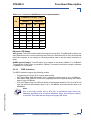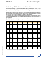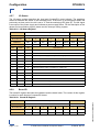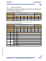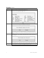
1
CP6500-V
Manual ID: 28945, Rev. Index 01
04 March, 2005
28945.01.UG.VC.050304/090948
USER GUIDE
The product described in this manual is
in compliance with all applied CE standards.
PRELIMINARY
6U CompactPCI
Intel® Celeron® Based CPU Board
Preface
CP6500-V
Revision History
Publication Title: CP6500-V: 6U CompactPCI Intel® Celeron® Based CPU Board
ID Number: 28945
Rev.
Index
User Guide
Date of Issue
04 Mar, 2005
Imprint
Kontron Modular Computers GmbH may be contacted via the following:
MAILING ADDRESS
TELEPHONE AND E-MAIL
Kontron Modular Computers GmbH
Sudetenstraße 7
D - 87600 Kaufbeuren Germany
+49 (0) 800-SALESKONTRON
[email protected]
For further information about other Kontron Modular Computers products, please visit our
Internet web site: www.kontron.com
Copyright
Copyright © 2005 Kontron Modular Computers GmbH. All rights reserved. This manual may
not be copied, photocopied, reproduced, translated or converted to any electronic or machinereadable form in whole or in part without prior written approval of Kontron Modular Computers.
GmbH.
Disclaimer:
Kontron Modular Computers GmbH rejects any liability for the correctness and
completeness of this manual as well as its suitability for any particular purpose.
Page ii
© 2005 Kontron Modular Computers GmbH
ID 28945, Rev. 01
28945.01.UG.VC.050304/090948
PRELIMINARY
01
Brief Description of Changes
CP6500-V
Preface
Revision History .........................................................................................................ii
Imprint ........................................................................................................................ii
Copyright ....................................................................................................................ii
Table of Contents ...................................................................................................... iii
List of Tables .............................................................................................................ix
List of Figures ...........................................................................................................xi
Proprietary Note ...................................................................................................... xiii
Trademarks ............................................................................................................. xiii
Environmental Protection Statement ....................................................................... xiii
Explanation of Symbols .......................................................................................... xiv
For Your Safety ........................................................................................................xv
High Voltage Safety Instructions ..........................................................................xv
Special Handling and Unpacking Instructions .....................................................xv
General Instructions on Usage ............................................................................... xvi
Two Year Warranty ................................................................................................. xvii
Chapter
1.
1
Introduction .................................................................................................. 1 - 3
1.1 System Overview .................................................................................... 1 - 3
1.2 Board Overview ....................................................................................... 1 - 4
1.2.1
Board Introduction .......................................................................... 1 - 4
1.2.2
Board-Specific Information ............................................................. 1 - 5
1.3 System Expansion Capabilities ............................................................... 1 - 6
1.3.1
PMC Modules ................................................................................. 1 - 6
1.3.2
CP-CTM80-2 Rear I/O Module ....................................................... 1 - 6
1.4 System Relevant Information .................................................................. 1 - 6
28945.01.UG.VC.050304/090948
1.5 Board Diagrams ...................................................................................... 1 - 7
1.5.1
Functional Block Diagram ............................................................... 1 - 7
1.5.2
Front Panels ................................................................................... 1 - 8
1.5.3
Board Layout .................................................................................. 1 - 9
1.6 Technical Specification .......................................................................... 1 - 11
1.7 Applied Standards ................................................................................. 1 - 15
1.8 Kontron Software Support ..................................................................... 1 - 16
ID 28945, Rev. 01
© 2005 Kontron Modular Computers GmbH
Page iii
PRELIMINARY
Table of Contents
Preface
CP6500-V
1.9 Related Publications ..............................................................................1 - 16
Chapter
2.
2
Functional Description .................................................................................2 - 3
2.1.1
CPU .................................................................................................2 - 3
2.1.2
Memory ...........................................................................................2 - 4
2.1.3
815-B0 Chipset Overview ................................................................2 - 4
2.1.4
Graphics and Memory Controller Hub (815-B0) ..............................2 - 5
2.1.5
I/O Controller Hub ICH4 ..................................................................2 - 5
2.2 Peripherals ...............................................................................................2 - 6
2.2.1
Timer ...............................................................................................2 - 6
2.2.2
Watchdog Timer ..............................................................................2 - 6
2.2.3
Battery .............................................................................................2 - 6
2.2.4
Reset ...............................................................................................2 - 7
2.2.5
SMBus Devices ...............................................................................2 - 7
2.2.6
Thermal Management/System Monitoring ......................................2 - 7
2.2.7
Serial EEPROM ..............................................................................2 - 8
2.2.8
FLASH Memory ...............................................................................2 - 8
2.2.8.1
BIOS FLASH (Firmware Hub) .................................................2 - 8
2.2.8.2
CompactFlash Socket .............................................................2 - 8
2.2.9
Front Panel LEDs ............................................................................2 - 9
2.2.9.1
Watchdog and Overtemperature LEDs .................................2 - 10
2.2.9.2
Front-I and Front-II General Purpose LEDs ..........................2 - 10
2.2.9.3
Hot Swap LED ......................................................................2 - 10
2.2.10 Keyboard/Mouse Interface ............................................................2 - 10
2.2.11 USB Interfaces .............................................................................. 2 - 11
2.2.12 Graphics Controller .......................................................................2 - 12
2.2.12.1
Video Memory Usage ...........................................................2 - 12
2.2.12.2
Video Resolution ...................................................................2 - 13
2.2.12.3
CRT Interface and Connector J10 ........................................2 - 14
2.2.13 COM Port ......................................................................................2 - 15
Page iv
© 2005 Kontron Modular Computers GmbH
ID 28945, Rev. 01
28945.01.UG.VC.050304/090948
PRELIMINARY
2.1 CPU, Memory and Chipset ......................................................................2 - 3
CP6500-V
Preface
2.2.14 Floppy Drive Interface ................................................................... 2 - 16
2.2.15 Fast Ethernet ................................................................................ 2 - 16
2.2.16 EIDE Interfaces ............................................................................. 2 - 17
2.2.16.1
EIDE 44-Pin Connector J19 ................................................. 2 - 19
2.2.16.2
EIDE 40-Pin Connector J20 ................................................. 2 - 20
2.2.17 Extension Connector J12 .............................................................. 2 - 20
2.2.18 PMC Interface ............................................................................... 2 - 21
2.2.18.1
PMC Connectors J23, J24, and J25 Pinouts
..................... 2 - 22
2.2.19.1
System Master Configuration ............................................... 2 - 24
2.2.19.2
PCI-to-PCI Bridge ................................................................ 2 - 24
2.2.19.3
Peripheral Master Configuration (Passive Mode) ................ 2 - 24
2.2.19.4
Packet Switching Backplane (PICMG 2.16) ......................... 2 - 24
2.2.19.5
Hot Swap Support ................................................................ 2 - 24
2.2.19.6
Power Ramping .................................................................... 2 - 25
2.2.19.7
Precharge ............................................................................. 2 - 25
2.2.19.8
Handle Switch ...................................................................... 2 - 25
2.2.19.9
ENUM# Interrupt .................................................................. 2 - 25
2.2.19.10 Hot Swap LED ...................................................................... 2 - 25
2.2.20 CompactPCI Bus Connector ......................................................... 2 - 26
2.2.20.1
CompactPCI Connector Keying ........................................... 2 - 26
2.2.20.2
CompactPCI Connectors J1 and J2 Pinouts ........................ 2 - 27
2.2.20.3
CompactPCI Rear I/O Connectors J3-J5 and Pinouts ......... 2 - 31
2.2.20.4
Rear I/O Configuration ......................................................... 2 - 35
Chapter
3.
3
Installation ................................................................................................... 3 - 3
28945.01.UG.VC.050304/090948
3.1 Safety Requirements ............................................................................... 3 - 3
3.2 CP6500-V Initial Installation Procedures ................................................. 3 - 4
3.3 Standard Removal Procedures ............................................................... 3 - 5
3.4 Hot Swap Procedures ............................................................................. 3 - 5
3.4.1
System Master Hot Swap ............................................................... 3 - 5
ID 28945, Rev. 01
© 2005 Kontron Modular Computers GmbH
Page v
PRELIMINARY
2.2.19 CompactPCI Interface .................................................................. 2 - 24
Preface
3.4.2
CP6500-V
Peripheral Hot Swap Procedure ......................................................3 - 6
3.5 Installation of CP6500-V Peripheral Devices ...........................................3 - 7
3.5.1
CompactFlash Installation ...............................................................3 - 7
3.5.2
USB Device Installation ...................................................................3 - 7
3.5.3
Rear I/O Device Installation .............................................................3 - 8
3.5.4
Battery Replacement .......................................................................3 - 8
3.5.5
Hard Disk Installation ......................................................................3 - 8
Chapter
4.
4
Configuration ................................................................................................4 - 3
4.1 Jumper Description ..................................................................................4 - 3
4.1.1
CompactFlash Configuration ..........................................................4 - 3
4.1.2
CompactFlash Power Configuration ................................................4 - 3
4.1.3
Clearing BIOS CMOS Setup ...........................................................4 - 3
4.1.4
Shorting Chassis GND (Shield) to Logic GND ................................4 - 4
4.1.5
VGA CRT Rear I/O Configuration ...................................................4 - 4
4.1.6
Front-I and Front-II General Purpose LEDs ....................................4 - 4
4.1.7
Serial Ports COM1 and COM2 Jumper and Resistor Settings ........4 - 5
4.1.7.1
COM1 Jumper and Resistor Setting .......................................4 - 5
4.1.7.2
COM2 Jumper and Resistor Setting .......................................4 - 6
4.2 Interrupts ..................................................................................................4 - 8
4.3 Onboard PCI Interrupt Routing ................................................................4 - 9
4.4 Memory Map ............................................................................................4 - 9
4.4.1
Memory Map for the 1st Megabyte .................................................4 - 9
4.4.2
I/O Address Map ...........................................................................4 - 10
4.5 Special Registers Description ................................................................ 4 - 11
4.5.1
Watchdog ...................................................................................... 4 - 11
4.5.2
Watchdog Trigger .......................................................................... 4 - 11
4.5.3
Watchdog Timer Register ..............................................................4 - 12
4.5.4
Geographic Addressing Register ..................................................4 - 13
4.5.5
Watchdog, CompactPCI Interrupt Configuration Register .............4 - 14
Page vi
© 2005 Kontron Modular Computers GmbH
ID 28945, Rev. 01
28945.01.UG.VC.050304/090948
PRELIMINARY
3.6 Software Installation ................................................................................3 - 9
CP6500-V
Preface
4.5.6
CPCI Master Reset ....................................................................... 4 - 15
4.5.7
I/O Status ...................................................................................... 4 - 16
4.5.8
Board ID ........................................................................................ 4 - 16
4.5.9
Hardware Index Register .............................................................. 4 - 17
4.5.10 Hot Swap Control Register ........................................................... 4 - 17
4.5.11 Logic Version Register .................................................................. 4 - 18
4.5.12 LED Control Register .................................................................... 4 - 18
Chapter
5.
BIOS ............................................................................................................ 5 - 3
Chapter
6.
5
6
Power Consumption .................................................................................... 6 - 3
6.1 System Power ......................................................................................... 6 - 3
6.1.1
CP6500-V Baseboard ..................................................................... 6 - 3
6.1.2
Backplane ....................................................................................... 6 - 4
6.1.3
Power Supply Units ........................................................................ 6 - 4
6.1.3.1
Start-Up Requirement ............................................................ 6 - 5
6.1.3.2
Power-Up Sequence .............................................................. 6 - 5
6.1.3.3
Tolerance ................................................................................ 6 - 5
6.1.3.4
Regulation .............................................................................. 6 - 6
6.1.3.5
Rise Time Diagram ................................................................ 6 - 6
28945.01.UG.VC.050304/090948
6.2 Power Consumption ................................................................................ 6 - 7
6.2.1
Real Applications ............................................................................ 6 - 7
6.2.2
Power Consumption of CP6500-V Accessories ............................ 6 - 8
6.2.3
Power Requirement for the CP6500-V ................................................6 - 8
ID 28945, Rev. 01
© 2005 Kontron Modular Computers GmbH
Page vii
PRELIMINARY
4.5.13 Hot Swap LED Control Register ................................................... 4 - 19
Preface
CP6500-V
Chapter
7.
7
System Considerations ................................................................................7 - 3
7.1 Passive Thermal Regulation ....................................................................7 - 3
7.1.1
CPU External Thermal Supervision ................................................7 - 3
7.1.2
CPU Emergency Thermal Supervision ...........................................7 - 4
7.1.3
Thermal Management Recommendations ......................................7 - 4
7.2.1
Heat Sinks .......................................................................................7 - 4
7.2.2
Forced Air Flow ...............................................................................7 - 5
7.2.3
Peripherals ......................................................................................7 - 6
Annex
A.
A
CP-CTM80-2 RIO Module ........................................................................... A - 3
A.1 Introduction ............................................................................................. A - 3
Annex
B.
B
AMIBIOS8 ................................................................................................... B - 3
28945.01.UG.VC.050304/090948
PRELIMINARY
7.2 Active Thermal Regulation .......................................................................7 - 4
Page viii
© 2005 Kontron Modular Computers GmbH
ID 28945, Rev. 01
CP6500-V
Preface
1-1
System Relevant Information .................................................................... 1 - 6
1-2
CP6500-V Main Specifications ................................................................ 1 - 11
1-3
Applied Standards ................................................................................... 1 - 15
1-4
Related Publications ................................................................................ 1 - 16
2-1
Supported Intel Celeron Processors on the CP6500-V ............................. 2 - 3
2-2
Maximum Power Dissipation of Intel Celeron (CPU only) ......................... 2 - 3
2-3
SM Bus Device Addresses ........................................................................ 2 - 7
2-4
EEPROM Address Map ............................................................................. 2 - 8
2-5
CompactFlash Connector J14 Pinout ........................................................ 2 - 9
2-6
Keyboard Connector J22 Pinout .............................................................. 2 - 10
2-7
USB Connectors J7 and J8 Pinout .......................................................... 2 - 11
2-8
Partial List of Display Modes Supported .................................................. 2 - 13
2-9
CRT Connector J10 Pinout ...................................................................... 2 - 14
2-10 Serial Port Connectors CON9 (COM1) Pinout ........................................ 2 - 15
2-11 Pinouts of J6A/B Based on the Implementation ...................................... 2 - 17
2-12 Pinout of EIDE Connector J19 ................................................................. 2 - 19
2-13 Pinout of EIDE Connector J20 ................................................................. 2 - 20
2-14 PMC Connectors J23 and J25 Pinouts .................................................... 2 - 22
2-15 PMC Connector J24 Pinouts ................................................................... 2 - 23
2-16 Coding Key Colors on J1 ......................................................................... 2 - 26
2-17 CompactPCI Bus Connector J1 System Slot Pinout .............................. 2 - 27
2-18 CompactPCI Bus Connector J1 Peripheral Slot Pinout ........................... 2 - 28
2-19 64-bit CompactPCI Bus Connector J2 System Slot Pinout .................... 2 - 29
2-20 64-bit CompactPCI Bus Connector J2 Peripheral Slot Pinout ................. 2 - 30
2-21 Backplane J3 Pinout ................................................................................ 2 - 31
2-22 Backplane J3 Signals .............................................................................. 2 - 32
2-23 Backplane J4 Pinout ................................................................................ 2 - 33
28945.01.UG.VC.050304/090948
2-24 Backplane J5 Pinout ................................................................................ 2 - 34
2-25 Backplane J5 Signals .............................................................................. 2 - 34
4-1
CompactFlash Configuration ..................................................................... 4 - 3
4-2
CompactFlash Power Configuration .......................................................... 4 - 3
4-3
Clearing BIOS CMOS Setup ..................................................................... 4 - 3
ID 28945, Rev. 01
© 2005 Kontron Modular Computers GmbH
Page ix
PRELIMINARY
List of Tables
Preface
CP6500-V
4-4
Shorting Chassis GND (Shield) to Logic GND ........................................... 4 - 4
4-5
VGA-CRT Jumper Setting .......................................................................... 4 - 4
4-6
General Purpose LED Setting .................................................................... 4 - 4
4-7
Resistor Setting to Configure COM1 .......................................................... 4 - 5
4-8
Jumper Setting for RS422 RXD Termination (COM1) ................................ 4 - 5
4-10 Resistor Setting to Configure COM2 .......................................................... 4 - 6
4-9
Jumper Setting for RS422 TXD and RS485 Termination (COM1) ............. 4 - 6
4-11 Jumper Setting for RS422 RXD Termination (COM2) ................................ 4 - 7
4-12 Jumper Setting for RS422 TXD and RS485 Termination (COM2) ............. 4 - 7
4-14 PCI Interrupt Routing ................................................................................. 4 - 9
4-15 Memory Map for the 1st Megabyte ............................................................ 4 - 9
4-16 I/O Address Map ...................................................................................... 4 - 10
4-17 Watchdog Timer Register ........................................................................ 4 - 12
4-18 Geographic Addressing Register ............................................................. 4 - 13
4-19 Watchdog, CompactPCI Interrupt Configuration Register ....................... 4 - 14
4-20 CPCI Master Reset Register .................................................................... 4 - 15
4-21 I/O Status Register ................................................................................... 4 - 16
4-22 Board ID Register .................................................................................... 4 - 16
4-23 Hardware Index Register ........................................................................ 4 - 17
4-24 Hot Swap Control Register ....................................................................... 4 - 17
4-25 Logic Version Register ............................................................................ 4 - 18
4-26 LED Control Register ............................................................................... 4 - 18
4-27 Hot Swap LED Control Register .............................................................. 4 - 19
6-1
Maximum Input Power Voltage Limits ........................................................ 6 - 3
6-2
DC Operational Input Voltage Ranges ....................................................... 6 - 3
6-3
Input Voltage Characteristics ..................................................................... 6 - 5
6-4
Power Consumption: DOS ......................................................................... 6 - 7
6-5
Power Consumption: Windows® 2000 IDLE Mode .................................... 6 - 7
6-6
Power Consumption: Windows® 2000 100% CPU Usage ........................ 6 - 8
6-7
Power Consumption Table for CP6500-V Accessories .............................. 6 - 8
6-8
Start-Up Current of the CP6500-V ............................................................. 6 - 8
Page x
© 2005 Kontron Modular Computers GmbH
ID 28945, Rev. 01
28945.01.UG.VC.050304/090948
PRELIMINARY
4-13 Interrupt Setting .......................................................................................... 4 - 8
CP6500-V
Preface
CP6500-V Functional Block Diagram ...................................................... 1 - 7
1-2
CP6500-V 4 HP Front Panel .................................................................... 1 - 8
1-3
CP6500-V Board Layout (Top View) ........................................................ 1 - 9
1-4
CP6500-V Board Layout (Bottom View) ................................................ 1 - 10
2-1
815-B0 Chipset Functional Block Diagram .............................................. 2 - 4
2-2
Keyboard Connector J22 ....................................................................... 2 - 10
2-3
USB Connectors J7 and J8 .................................................................... 2 - 11
2-4
D-SUB CRT Connector J10 ................................................................... 2 - 14
2-5
PC-Compatible D-SUB Serial Connectors J9 (COM1) .......................... 2 - 15
2-6
Dual Fast Ethernet Connector J6A/B .................................................... 2 - 16
2-7
EIDE Interface Connectors J19 and J20 ................................................ 2 - 18
2-8
Extension Connector J12 ....................................................................... 2 - 20
2-9
PMC Connectors J23, J24, and J25 ...................................................... 2 - 21
2-10
CompactPCI Connectors J1-J5 ............................................................ 2 - 26
4-1
COM1 Configuration Jumpers and Resistors .......................................... 4 - 5
4-2
COM2 Configuration Jumpers and Resistors ......................................... 4 - 6
6-1
Start-Up Ramp of the CP3-SVE180 AC Power Supply ............................ 6 - 6
7-1
Celeron Temperature Vs. Airspeed Graph with Heat Sink ..................... 7 - 5
A-1
CP-CTM80-2 RIO Module, 4HP Variant .................................................. A - 4
28945.01.UG.VC.050304/090948
1-1
ID 28945, Rev. 01
© 2005 Kontron Modular Computers GmbH
Page xi
PRELIMINARY
List of Figures
PRELIMINARY
Preface
CP6500-V
28945.01.UG.VC.050304/090948
This page has been intentionally left blank.
Page xii
© 2005 Kontron Modular Computers GmbH
ID 28945, Rev. 01
CP6500-V
Preface
Proprietary Note
This document contains information proprietary to Kontron Modular Computers GmbH. It may
not be copied or transmitted by any means, disclosed to others, or stored in any retrieval
system or media without the prior written consent of Kontron Modular Computers GmbH or one
of its authorized agents.
The information contained in this document is, to the best of our knowledge, entirely correct.
However, Kontron Modular Computers GmbH cannot accept liability for any inaccuracies or the
consequences thereof, or for any liability arising from the use or application of any circuit,
product, or example shown in this document.
Trademarks
Kontron Modular Computers GmbH, the PEP logo and, if occurring in this manual, “CXM” are
trademarks owned by Kontron Modular Computers GmbH, Kaufbeuren (Germany). In addition,
this document may include names, company logos and trademarks, which are registered trademarks and, therefore, proprietary to their respective owners.
Environmental Protection Statement
This product has been manufactured to satisfy environmental protection requirements where
possible. Many of the components used (structural parts, printed circuit boards, connectors,
batteries, etc.) are capable of being recycled.
28945.01.UG.VC.050304/090950
Final disposition of this product after its service life must be accomplished in accordance with
applicable country, state, or local laws or regulations.
ID 28945, Rev. 01
© 2005 Kontron Modular Computers GmbH
Page xiii
PRELIMINARY
Kontron Modular Computers GmbH reserves the right to change, modify, or improve this
document or the product described herein, as seen fit by Kontron Modular Computers GmbH
without further notice.
Preface
CP6500-V
Explanation of Symbols
CE Conformity
This symbol indicates that the product described in this manual is in
compliance with all applied CE standards. Please refer also to the
section “Applied Standards” in this manual.
Caution, Electric Shock!
This symbol and title warn of hazards due to electrical shocks (> 60V)
when touching products or parts of them. Failure to observe the precautions indicated and/or prescribed by the law may endanger your
life/health and/or result in damage to your material.
PRELIMINARY
Please refer also to the section “High Voltage Safety Instructions” on
the following page.
Warning, ESD Sensitive Device!
This symbol and title inform that electronic boards and their components are sensitive to static electricity. Therefore, care must be taken
during all handling operations and inspections of this product, in
order to ensure product integrity at all times.
Please read also the section “Special Handling and Unpacking
Instructions” on the following page.
Warning!
This symbol and title emphasize points which, if not fully understood
and taken into consideration by the reader, may endanger your health
and/or result in damage to your material.
Note ...
28945.01.UG.VC.050304/090950
This symbol and title emphasize aspects the reader should read
through carefully for his or her own advantage.
Page xiv
© 2005 Kontron Modular Computers GmbH
ID 28945, Rev. 01
CP6500-V
Preface
For Your Safety
Your new Kontron product was developed and tested carefully to provide all features
necessary to ensure its compliance with electrical safety requirements. It was also designed
for a long fault-free life. However, the life expectancy of your product can be drastically reduced
by improper treatment during unpacking and installation. Therefore, in the interest of your own
safety and of the correct operation of your new Kontron product, you are requested to conform
with the following guidelines.
High Voltage Safety Instructions
Warning!
Caution, Electric Shock!
Before installing your new Kontron product into a system always
ensure that your mains power is switched off. This applies also to the
installation of piggybacks.
Serious electrical shock hazards can exist during all installation,
repair and maintenance operations with this product. Therefore,
always unplug the power cable and any other cables which provide
external voltages before performing work.
Special Handling and Unpacking Instructions
ESD Sensitive Device!
Electronic boards and their components are sensitive to static electricity. Therefore, care must be taken during all handling operations
and inspections of this product, in order to ensure product integrity at
all times.
28945.01.UG.VC.050304/090950
Do not handle this product out of its protective enclosure while it is not used for operational
purposes unless it is otherwise protected.
Whenever possible, unpack or pack this product only at EOS/ESD safe work stations. Where
a safe work station is not guaranteed, it is important for the user to be electrically discharged
before touching the product with his/her hands or tools. This is most easily done by touching a
metal part of your system housing.
It is particularly important to observe standard anti-static precautions when changing piggybacks, ROM devices, jumper settings etc. If the product contains batteries for RTC or memory
backup, ensure that the board is not placed on conductive surfaces, including anti-static plastics or sponges. They can cause short circuits and damage the batteries or conductive circuits
on the board.
ID 28945, Rev. 01
© 2005 Kontron Modular Computers GmbH
Page xv
PRELIMINARY
All operations on this device must be carried out by sufficiently skilled
personnel only.
Preface
CP6500-V
General Instructions on Usage
In order to maintain Kontron’s product warranty, this product must not be altered or modified in
any way. Changes or modifications to the device, which are not explicitly approved by Kontron
Modular Computers GmbH and described in this manual or received from Kontron Modular
Computers’ Technical Support as a special handling instruction, will void your warranty.
This device should only be installed in or connected to systems that fulfill all necessary
technical and specific environmental requirements. This applies also to the operational
temperature range of the specific board version, which must not be exceeded. If batteries are
present, their temperature restrictions must be taken into account.
Keep all the original packaging material for future storage or warranty shipments. If it is
necessary to store or ship the board, please re-pack it as nearly as possible in the manner in
which it was delivered.
Special care is necessary when handling or unpacking the product. Please consult the special
handling and unpacking instruction on the previous page of this manual.
28945.01.UG.VC.050304/090950
PRELIMINARY
In performing all necessary installation and application operations, please follow only the
instructions supplied by the present manual.
Page xvi
© 2005 Kontron Modular Computers GmbH
ID 28945, Rev. 01
CP6500-V
Preface
Two Year Warranty
Kontron Modular Computers GmbH grants the original purchaser of Kontron’s products a TWO
as described in the following. However, no other warranties that may be granted or implied by anyone on behalf of Kontron are valid unless the consumer has the express written consent of Kontron Modular Computers GmbH.
Kontron Modular Computers GmbH warrants their own products, excluding software, to be free
from manufacturing and material defects for a period of 24 consecutive months from the date
of purchase. This warranty is not transferable nor extendible to cover any other users or longterm storage of the product. It does not cover products which have been modified, altered or
repaired by any other party than Kontron Modular Computers GmbH or their authorized agents.
Furthermore, any product which has been, or is suspected of being damaged as a result of negligence, improper use, incorrect handling, servicing or maintenance, or which has been damaged as a result of excessive current/voltage or temperature, or which has had its serial
number(s), any other markings or parts thereof altered, defaced or removed will also be excluded from this warranty.
If the customer’s eligibility for warranty has not been voided, in the event of any claim, he may
return the product at the earliest possible convenience to the original place of purchase, together with a copy of the original document of purchase, a full description of the application the
product is used on and a description of the defect. Pack the product in such a way as to ensure
safe transportation (see our safety instructions).
Kontron provides for repair or replacement of any part, assembly or sub-assembly at their own
discretion, or to refund the original cost of purchase, if appropriate. In the event of repair, refunding or replacement of any part, the ownership of the removed or replaced parts reverts to
Kontron Modular Computers GmbH, and the remaining part of the original guarantee, or any
new guarantee to cover the repaired or replaced items, will be transferred to cover the new or
repaired items. Any extensions to the original guarantee are considered gestures of goodwill,
and will be defined in the “Repair Report” issued by Kontron with the repaired or replaced item.
28945.01.UG.VC.050304/090950
Kontron Modular Computers GmbH will not accept liability for any further claims resulting
directly or indirectly from any warranty claim, other than the above specified repair,
replacement or refunding. In particular, all claims for damage to any system or process in which
the product was employed, or any loss incurred as a result of the product not functioning at any
given time, are excluded. The extent of Kontron Modular Computers GmbH liability to the
customer shall not exceed the original purchase price of the item for which the claim exists.
Kontron Modular Computers GmbH issues no warranty or representation, either explicit or
implicit, with respect to its products’ reliability, fitness, quality, marketability or ability to fulfil any
particular application or purpose. As a result, the products are sold “as is,” and the
responsibility to ensure their suitability for any given task remains that of the purchaser. In no
event will Kontron be liable for direct, indirect or consequential damages resulting from the use
of our hardware or software products, or documentation, even if Kontron were advised of the
possibility of such claims prior to the purchase of the product or during any period since the
date of its purchase.
Please remember that no Kontron Modular Computers GmbH employee, dealer or agent is
authorized to make any modification or addition to the above specified terms, either verbally or
in any other form, written or electronically transmitted, without the company’s consent.
ID 28945, Rev. 01
© 2005 Kontron Modular Computers GmbH
Page xvii
PRELIMINARY
YEAR LIMITED HARDWARE WARRANTY
PRELIMINARY
Preface
CP6500-V
28945.01.UG.VC.050304/090950
This page has been intentionally left blank.
Page xviii
© 2005 Kontron Modular Computers GmbH
ID 28945, Rev. 01
Introduction
Chapter
1
28945.01.UG.VC.050304/090951
Introduction
ID 28945, Rev. 01
© 2005 Kontron Modular Computers GmbH
Page 1 - 1
PRELIMINARY
CP6500-V
PRELIMINARY
Introduction
CP6500-V
28945.01.UG.VC.050304/090951
This page has been intentionally left blank.
Page 1 - 2
© 2005 Kontron Modular Computers GmbH
ID 28945, Rev. 01
CP6500-V
Introduction
1.
Introduction
1.1
System Overview
Many system-relevant CompactPCI features that are specific to Kontron Modular Computers
CompactPCI systems may be found described in the Kontron CompactPCI System Manual.
Due to its size, this manual cannot be downloaded via the internet. Please refer to the section
“Related Publications” at the end of this chapter for the relevant ordering information.
The CompactPCI System Manual includes the following information:
28945.01.UG.VC.050304/090951
• Common information that is applicable to all system components, such as safety
information, warranty conditions, standard connector pinouts etc.
• All the information necessary to combine Kontron’s racks, boards, backplanes, power
supply units and peripheral devices in a customized CompactPCI system, as well as
configuration examples.
• Data on rack dimensions and configurations as well as information on mechanical and
electrical rack characteristics.
• Information on the distinctive features of Kontron CompactPCI boards, such as
functionality, hot swap capability. In addition, an overview is given for all existing Kontron
CompactPCI boards with links to the relating data sheets.
• Generic information on the Kontron CompactPCI backplanes, such as the slot
assignment, PCB form factor, distinctive features, clocks, power supply connectors and
signalling environment, as well as an overview of the Kontron CompactPCI standard
backplane family.
• Generic information on the Kontron CompactPCI power supply units, such as the input/
output characteristics, redundant operation and distinctive features, as well as an
overview of the Kontron CompactPCI standard power supply unit family.
ID 28945, Rev. 01
© 2005 Kontron Modular Computers GmbH
Page 1 - 3
PRELIMINARY
The CompactPCI board described in this manual operates with the PCI bus architecture to
support additional I/O and memory-mapped devices as required by various industrial
applications. For detailed information concerning the CompactPCI standard, please consult the
complete Peripheral Component Interconnect (PCI) and CompactPCI Specifications. For
further information regarding these standards and their use, visit the home page of the
PCI Industrial Computer Manufacturers Group (PICMG).
Introduction
CP6500-V
1.2
Board Overview
1.2.1
Board Introduction
The CP6500-V is a highly integrated CompactPCI board that has been designed to support the
Intel® Celeron® processor, which is based on the same core as existing mobile processors. The
CP6500-V utilizes the Intel 815-B0 chipset and the ICH4 I/O Controller Hub. The CPU speed
ranges from 400 MHz through 1 GHz.
The CP6500-V comes with two Fast Ethernet ports, two USB 2.0 ports, two COM ports, two
EIDE interfaces, one PMC interface with 32-bit/33 MHz on the PCI bus (in accordance with the
PICMG 2.3 specification), a Low Pin Count interface (LPC), rear I/O with several interfaces,
one CompactFlash socket, and a built-in Intel 3D Graphics accelerator with a VGA CRT display
interface. Several onboard connectors provide flexible expendability.
The board supports a configurable 32-bit/33 MHz, hot swap CompactPCI interface. In the
System Master slot the interface is enabled, and if installed in a peripheral slot, the CP6500-V
is isolated from the CompactPCI bus.
One of the more important features of the CP6500-V is its support of the PICMG CompactPCI
Packet Switching Backplane Specification 2.16. When installed in a backplane which supports
packet switching, the CP6500-V can communicate via two Fast Ethernet interfaces with other
peripherals.
The board is offered with the Microsoft® Windows® 2000, Windows® XP and Windows® XP
Embedded operating systems. Kontron further supports, as a standard, Linux and VxWorks®.
Please contact Kontron Modular Computers for further information concerning other operating
systems.
28945.01.UG.VC.050304/090951
PRELIMINARY
To achieve high system performance, the board supports one SODIMM socket for a flexible
memory configuration, up to 512 MB SDRAM memory without Error Checking and Correcting
(ECC).The CP6500-V supports memory speed up to 100 MHz.
Page 1 - 4
© 2005 Kontron Modular Computers GmbH
ID 28945, Rev. 01
CP6500-V
1.2.2
Introduction
Board-Specific Information
The CP6500-V is a CompactPCI Celeron based single-board computer specifically designed
for use in highly integrated platforms with solid mechanical interfacing for a wide range of
industrial environment applications.
•
•
•
•
•
•
•
•
•
•
•
•
•
•
•
•
•
•
•
•
•
28945.01.UG.VC.050304/090951
•
•
•
•
•
•
•
•
•
•
Intel Celeron microprocessor
479-pin µFCBGA package
Up to 256 kB L2 cache on-die, running at CPU speed
100 MHz or 133 MHz processor system bus
815-B0 chipset
Up to 512 MB SDRAM memory
Integrated 3D VGA controller
Analog display support up to 1600 x 1200 pixels at 8-bit and 75 Hz
PMC interface (32-bit/33 MHz PCI, 3.3 V and 5 V) with rear I/O support and bezel cutout
on front panel and PCI functionality
Two Fast Ethernet interfaces on the front panel switchable to rear I/O (PICMG 2.16)
Two EIDE Ultra ATA/100 interfaces
Optional socket for 2.5" hard disk
Onboard CompactFlash type II socket (True IDE)
Four USB ports
• Two USB 2.0 ports on the front panel
• Two USB 2.0 ports on rear I/O
1 MB onboard FWH for BIOS
Hardware monitor integrated in Windbond Super I/O W83627HF
Floppy disk interface on rear I/O
One 32-bit PCI-to-PCI bridge at 33 MHz
Watchdog timer
Real-time clock
Two COM ports
• one switchable to front or rear I/O with RS232 or RS422
• one only for rear I/O with RS232/RS422/RS485
POST code or general purpose LEDs (Front-I and Front-II)
I/O extension connector (LPC)
4HP, 6U CompactPCI
Passive heat sink solution for external airflow
AMI BIOS
Compatible with CompactPCI spec. Rev. 2.3 (32-bit/33 MHz)
Hot swap capability: as system controller or as peripheral device
Supports PICMG Packet Switching Backplane Specification 2.16
Several rear I/O configurations
Rear I/O on J3, J4,and J5
ID 28945, Rev. 01
© 2005 Kontron Modular Computers GmbH
Page 1 - 5
PRELIMINARY
Some of the CP6500-V's outstanding features are:
Introduction
CP6500-V
1.3
System Expansion Capabilities
1.3.1
PMC Modules
The CP6500-V has one PCI, 32-bit/33 MHz, 3.3 V or 5 V, rear I/O capable, PMC mezzanine
interface. This interface supports a wide range of available PMC modules with PCI interface
including all of Kontron’s PMC modules and provides an easy and flexible way to configure the
CP6500-V for various application requirements.
1.3.2
CP-CTM80-2 Rear I/O Module
The CP-CTM80-2 rear I/O module has been designed for use with the CP6500-V 6U
CompactPCI board from Kontron Modular Computers. This module provides comprehensive
rear I/O functionality and may also be configured for use in other applications.
The CP-CTM80-2 rear I/O module provides only USB 1.1 ports.
For further information concerning the CP-CTM80-2 module, please refer to Appendix A.
1.4
System Relevant Information
The following system relevant information is general in nature but should still be considered
when developing applications using the CP6500-V.
Table 1-1:
System Relevant Information
SUBJECT
System Slot / System Master
Functionality
INFORMATION
The CP6500-V is designed for use as a System Master board whereby it can
support up to 7 peripheral boards with 32-bit / 33 MHz.
It may, however, be operated in a peripheral slot in which case it does not
support the CompactPCI bus interface.
Peripheral Slot Functionality
When installed in a peripheral slot, the CP6500-V is electrically isolated from
the CompactPCI bus. It receives power from the backplane and supports rear
I/O and, if the system supports it, packet switching (in this case up to two
channels of Fast Ethernet).
Hot Swap Compatibility
When operated as a System Master, the CP6500-V supports individual
clocks for each slot and ENUM signal handling is in compliance with the
PICMG 2.1 Hot Swap Specification.
When operated in a peripheral slot the CP6500-V supports basic hot swap.
Operating Systems
The CP6500-V can be operated under the following operating systems:
• Microsoft Windows 2000
• Microsoft Windows XP
• Microsoft Windows XP Embedded
• Linux
• VxWorks
Please contact Kontron Modular Computers for further information concerning other operating systems.
Page 1 - 6
© 2005 Kontron Modular Computers GmbH
ID 28945, Rev. 01
28945.01.UG.VC.050304/090951
PRELIMINARY
Note ...
CP6500-V
1.5
Introduction
Board Diagrams
The following diagrams provides additional information concerning board functionality and
component layout.
1.5.1
Functional Block Diagram
Figure 1-1:
CP6500-V Functional Block Diagram
J5
CPCI
Floppy
EIDE
Secondary
Local PMC
32-bit/33 MHz
J4
CPCI
PMC
REAR I/O
Fast
Ethernet
82551ER
J3
CPCI
VGA
COM1/2
KB/Mouse
USB3/4 2.0
PICMG 2.16
J1/J2
CPCI
Hot Swap
CPCI
32-bit/33 MHz
Hotswap
100 MHz
GMCH
815-B0
VGA
CRT
RTC
100 MHz/
133 MHz
Temp.
Monitor
Fast
Ethernet
82551ER
ICH4
I/O Hub
ULV/LV
Celeron
Power
Supply
LPC
BIOS
FWH
1 MB
COM1
9-pin
PCI-to-PCI
Bridge
CompactFlash
type I and II
2.5” HDD
Super
I/O
Keyboard
I/O
Ext.
Floppy
Ethernet
RJ45
Primary EIDE
EIDE
USB 2.0
4-pin
Ethernet
RJ45
USB 2.0
4-pin
Secondary EIDE
Front Panel Connectors
Bus Connectors
Onboard Connectors
28945.01.UG.VC.050304/090951
CPU
ID 28945, Rev. 01
© 2005 Kontron Modular Computers GmbH
Page 1 - 7
PRELIMINARY
144-pin SDRAM
up to 512 MB
Introduction
1.5.2
CP6500-V
Front Panels
Figure 1-2: CP6500-V 4 HP Front Panel
Legend:
General Purpose LEDs
WD (green):
Watchdog, when lit during boot-up,
it indicates a PCI reset is active.
TH (green):
Overtemperature Status, when lit
during boot-up, it indicates a power
failure.
PRELIMINARY
HS (blue):
Hot Swap Control
Front-I:
General Purpose or POST code
Front-II:
General Purpose or POST code
Integral Ethernet LEDs
ACT (green):
SPEED (green/orange):
Ethernet Link/Activity
Ethernet Speed
100 Mbit
SPEED ON (green):
10 Mbit
28945.01.UG.VC.050304/090951
SPEED ON (orange):
Page 1 - 8
© 2005 Kontron Modular Computers GmbH
ID 28945, Rev. 01
CP6500-V
1.5.3
Introduction
Board Layout
Figure 1-3:
CP6500-V Board Layout (Top View)
22
2
21
1
J12
J16
J17
J22
J18 J21
1
2
1
2
FWH
63
J5
J25
64
63
1
64
2
PRELIMINARY
J23
CompactFlash
Socket
J24
SDRAM Socket
J4
63
64
J20
J10
815-B0
C1
39
40
1
2
2
1
44
43
J19
J3
J9
WD/TH LEDs
J8
J2
POST
CODE
LEDs
J7
ICH4
C3
CPU
C4
Fast
Eth.
PCI-toPCI
Bridge
J6
Fast
Eth.
28945.01.UG.VC.050304/090951
C5
HS LED & RST
J11
ID 28945, Rev. 01
J1
Battery
© 2005 Kontron Modular Computers GmbH
Page 1 - 9
Introduction
Figure 1-4:
CP6500-V
CP6500-V Board Layout (Bottom View)
JP7
R218 R199
R329
COM2
JP3
PRELIMINARY
JP8
R320
R215
JP4
R330
R311
COM1
JP5
JP6
JP1
C63
C224
28945.01.UG.VC.050304/090951
C64
C205
Page 1 - 10
© 2005 Kontron Modular Computers GmbH
ID 28945, Rev. 01
CP6500-V
1.6
Introduction
Technical Specification
Table 1-2:
CP6500-V Main Specifications
CP6500-V
CPU
SPECIFICATIONS
The CP6500-V supports the following microprocessors:
• Intel Celeron with 256 kB L2 cache
• 400 MHz version with 100 MHz PSB in 479 µFCBGA
• 1.0 GHz version with 133 MHz PSB in 479 µFCBGA
Memory
Main Memory:
Processor and Memory
• Up to 512 MB SDRAM memory without ECC via one 144-pin SODIMM
socket running at 100 MHz
• 32 kB L1 on-die full speed processor cache
• 16 kB for instruction cache
• 16 kB for write-back data cache
• Up to 256 kB L2 on-die full speed processor cache
FLASH Memory:
• 8 Mbit Firmware Hub (FWH) for BIOS
Memory Extension:
• CompactFlash socket type II (true IDE mode with DMA capability)
Serial EEPROM:
• 24LC64 (8 kB) for storing CMOS data when operating without battery
Intel 815-B0 GMCH
815-B0 Graphics Memory Controller Hub (GMCH)
• Support for a single Celeron microprocessor
• 64-bit AGTL-based System Bus interface at 100 MHz for 400 MHz processor and 133 MHz for 1GHz processor
• 64-bit System Memory interface with support for SDRAM memory at
Chipsets
100 MHz
• Integrated 2D and 3D Graphics Engines
• Integrated H/W Motion Compensation Engine
• Integrated 230 MHz DAC
Intel ICH4 Chipset
Intel ICH4 I/O Controller Hub
•
•
•
•
•
28945.01.UG.VC.050304/090951
•
•
•
PCI Rev. 2.2 compliant with support for 32-bit/33 MHz PCI operations
Power management logic support
Enhanced DMA controller, interrupt controller, and timer functions
Integrated IDE controller Ultra ATA/100/33
USB 2.0 host interface with up to four USB ports available on the
CP6500-V
System Management Bus (SMBus) compatible with most I²C™ devices
Low Pin Count (LPC) interface
Firmware Hub (FWH) interface support
ID 28945, Rev. 01
© 2005 Kontron Modular Computers GmbH
Page 1 - 11
PRELIMINARY
Cache structure:
Introduction
Table 1-2:
CP6500-V Main Specifications (Continued)
CP6500-V
SPECIFICATIONS
CompactPCI
Compliant with CompactPCI Specification PICMG ® 2.0 R 3.0
• System Master operation
• 32-bit / 33 MHz master interface
• 3.3 V and 5.0 V compliant (default configuration: 5V)
When the CP6500-V is operated in a peripheral slot, the CPCI bus is electrically isolated (passive mode).
Rear I/O
The following interfaces are routed to the rear I/O connector J3, J4 and J5:
• COM1 and COM2 (RS232, RS422 and RS485 signaling); no buffer on the
rear I/O module is necessary
• 2 x USB 2.0
• CRT VGA
• PS/2 (Mouse / Keyboard)
• 2 x Fast Ethernet (compliant with PICMG 2.16, R 1.0)
• Secondary EIDE (ATA 100)
• General purpose signals
• PMC rear I/O
• Floppy disk interface
Hot Swap Compatible
The CP6500-V supports System Master hot swap functionality and
application dependent hot swap functionality when used in a peripheral slot.
VGA
Built-in Intel 2D and 3D Graphics accelerator:
• Supports resolutions of up to 1600 x 1200 by 8-bit color resolution at a 75 Hz
refresh rate or up to 1280 x 1024 by 24-bit color resolution at an 85 Hz refresh rate.
• Hardware motion compensation for software MPEG2 and MPEG4 decoding
• The graphics controller provides flexible allocation of video memory up to
6 MB.
Fast Ethernet
Up to two 10 Base-T/100 Base-TX Fast Ethernet interfaces based on the Intel
82551ER Ethernet 32-bit PCI bus controller.
• Two channels on rear I/O
• Two RJ45 connectors on the front panel
• Automatic mode recognition
• Automatic cabling configuration recognition
Cabling requirement: Category 5, UTP
USB
Four USB ports supporting UHCI and EHCI:
• Two USB 2.0 connectors on the front panel
• Two USB 2.0 on the rear I/O interface
Serial
Two serial ports from Super I/O
• COM1 on the front panel or rear I/O
• COM2 on the rear I/O interface (RS232, RS422 and RS485 signaling)
PMC
CMC / PMC P1386 / Draft 2.4a compliant mezzanine interface
• J23, J24, and J25 PCI mezzanine connectors for standard PMC modules
• 32-bit / 33 MHz PCI interface
• 3.3 V and 5 V compatible (default configuration 5V)
• Rear I/O supported through the CompactPCI connector J4
Page 1 - 12
© 2005 Kontron Modular Computers GmbH
ID 28945, Rev. 01
28945.01.UG.VC.050304/090951
When used as a System Master the CP6500-V supports individual clocks for
each slot and ENUM signal handling is in compliance with the PICMG 2.1 Hot
Swap Specification, Rev. 2.0, January 17, 2001.
Interfaces
PRELIMINARY
CP6500-V
CP6500-V
CP6500-V Main Specifications (Continued)
CP6500-V
SPECIFICATIONS
Keyboard and mouse are supported
• USB Support
• PS/2 (keyboard and mouse) with rear I/O module (e.g. CP-CTM80-2)
• Separate onboard keyboard connector (5-pin) that requires an adapter in
order to be connected to a regular keyboard
Mass Storage
EIDE Ultra ATA/100/33:
• Two interfaces:
• One 44-pin, 2.0 mm male pinrow connector for onboard HDD
• One 40-pin, 2.54 mm, male pinrow connector
• Up to four devices (hard disks or CD-ROMs)
Interfaces
Keyboard and Mouse
Onboard 2.5" hard disk:
• Onboard 2.5" hard disk can be mounted to the 44-pin connector
CompactFlash:
• CompactFlash type II socket (true IDE mode with DMA capability)
• Supports type I and II CompactFlash cards and Microdrive
Floppy Disk (only with rear I/O module):
• Supports 5.25" or 3.5 " floppy drives
• 1.2 or 1.44 MB, 3.5" floppy disks
General
28945.01.UG.VC.050304/090951
Sockets
I/O Extension Interface
I/O extension interface
• LPC devices
Front Panel
Connectors
•
•
•
•
•
Onboard Connectors
• Two EIDE interfaces supporting Ultra ATA/100/33
• one 44-pin, 2.0 mm connector
• one 40-pin, 2.54 mm connector
• CompactFlash socket type II (primary EIDE interface)
• I/O extension connector
• PMC interface (connector Jn1 - Jn4)
• CompactPCI Connector J1 and J2 (J3 - J5 optional)
• 5-pin PS/2 connector (keyboard)
• 144-pin SODIMM connector
VGA: 15-pin, D-SUB connector
USB: two 4-pin connectors
Ethernet: up to two RJ-45 connectors
COM: 9-pin, D-SUB connector
PMC front panel
Mechanical
6U, 4HP, CompactPCI compliant form factor
Power Consumption
See Chapter 5 for details
Temperature Range
Operational: 0°C to 60°C
Storage:
-55°C to +85°C
Without hard disk
Climatic Humidity
93% RH at 40 °C, non-condensing (acc. to IEC 60068-2-78)
Dimensions
233.35 mm x 160 mm
Board Weight
443 g (with standard heat sink and without mezzanine boards)
Battery
3.0 V lithium battery for RTC with battery socket. Recommended types:
• VARTA CR2025
• PANASONIC BR2020
ID 28945, Rev. 01
© 2005 Kontron Modular Computers GmbH
Page 1 - 13
PRELIMINARY
Table 1-2:
Introduction
Introduction
Table 1-2:
CP6500-V
CP6500-V Main Specifications (Continued)
CP6500-V
LEDs
SPECIFICATIONS
System status:
• TH (green): Overtemperature Status, when remains lit during boot-up, it
indicates a power failure.
• WD (green): Watchdog, when remains lit during boot-up, it indicates a PCI
reset is active.
Fast Ethernet status:
HW Monitoring
General Purpose LEDs:
• I (green):
• II (green):
General Purpose or POST code
General Purpose or POST code
Watchdog
Software configurable two-stage watchdog with programmable timeout ranging
from 125 msec to 256 sec in 12 steps generates IRQ, NMI, or hardware reset.
Thermal Management
CPU overtemperature protection is provided by:
• CPU shut down via hardware monitor
• Custom-designed heat sinks
System Monitor
Integrated HW monitoring in Winbond Super I/O W83627HF for the supervision
of:
• Several system power voltages
• Two fan speed input
• CPU and system temperature
AMI BIOS with 1 MB of Flash memory and having the following features:
•
•
•
•
•
•
•
•
•
•
•
Operating Systems
Operating systems supported:
•
•
•
•
•
Page 1 - 14
QuickBo ot
QuietBoot
BootBlock
LAN boot capability for diskless systems (standard Etherboot / PXE on
demand)
Boot from USB devices
BIOS boot support for USB keyboards
Plug and Play capability
BIOS parameters are saved in the EEPROM
Board serial number is saved within the EEPROM
PC Health Monitoring
ACPI
Microsoft Windows 2000
Microsoft Windows XP
Microsoft Windows XP Embedded
Linux
VxWorks
© 2005 Kontron Modular Computers GmbH
28945.01.UG.VC.050304/090951
Software BIOS
Software
PRELIMINARY
• ACT (green):
network activity
• SPEED (green / orange): network speed
ID 28945, Rev. 01
CP6500-V
1.7
Introduction
Applied Standards
The Kontron Modular Computers’ CompactPCI systems comply with the requirements of the
following standards:
Table 1-3:
Applied Standards
COMPLIANCE
CE
TYPE
Emission
TEST LEVEL
(RUGGEDIZED VERSION)
STANDARD
EN55022
--
EN61000-6-3
Immission
EN55024
--
28945.01.UG.VC.050304/090951
EN61000-6-2
EN60950
--
Mechanical
Mechanical Dimensions
IEEE 1101.10
--
Environmental
and Health
Aspects
Vibration (Sinusoidal)
IEC60068-2-6
10-300 [Hz]
2 [g]
1 [oct/min]
10 cycles/axis
3 axes
Shock
IEC60068-2-27
30 [g]
9 [ms]
3 shocks per direction
6 directions
5 [s] recovery time
Bump
IEC60068-2-29
15 [g]
11 [ms]
500 bumps per direction
6 directions
1 [s] recovery time
Vibration, broad-band
random (digital control)
and guidance
IEC 60068-2-64
20-500Hz, 0.05[g²]
500-2000Hz, 0.005[g²]
3,5 [g RMS]
30 [min] test time/axis
3 axes
Climatic Humidity
IEC60068-2-78
93% RH at 40 °C, non-condensing
WEEE
Directive 2002/96/EC
Waste electrical and electronic
equipment
RoHS
Directive 2002/95/EC
Restriction of the use of certain
hazardous substances in electrical
and electronic equipment
PRELIMINARY
Electrical Safety
Note ...
The values in the above table are valid for boards which are ordered with the
ruggedized service. For more information, please contact your local Kontron
office.
ID 28945, Rev. 01
© 2005 Kontron Modular Computers GmbH
Page 1 - 15
Introduction
1.8
CP6500-V
Kontron Software Support
Kontron is one of the few CompactPCI and VME manufacturers providing inhouse support for
most of the industry-proven real-time operating systems that are currently available. Due to its
close relationship with the software manufacturers, Kontron is able to produce and support
BSPs and drivers for the latest operating system revisions thereby taking advantage of the
changes in technology.
Finally, customers possessing a maintenance agreement with Kontron can be guaranteed
hotline software support and are supplied with regular software updates. A dedicated web site
is also provided for online updates and release downloads.
1.9
Related Publications
Table 1-4:
Related Publications
PRODUCT
CompactPCI Systems and
Boards
PUBLICATION
CompactPCI Specification 2.0, Rev. 3.0
CompactPCI Packet Switching Backplane Specification PICMG 2.16 Rev. 2.0
CompactPCI System Management Specification PICMG 2.9 Rev. 1.0
CompactPCI Hot Swap Specification PICMG 2.1 Rev. 2.0
Hot Swap Specification PICMG 2.1
Kontron Modular Computers’ CompactPCI System Manual, ID 19954
CompactFlash Cards
CF+ and CompactFlash Specification Revision 1.4
28945.01.UG.VC.050304/090951
PRELIMINARY
The following publications contain information relating to this product.
Page 1 - 16
© 2005 Kontron Modular Computers GmbH
ID 28945, Rev. 01
Functional Description
Chapter
21
28945.01.UG.VC.050304/090952
Functional Description
ID 28945, Rev. 01
© 2005 Kontron Modular Computers GmbH
Page 2 - 1
PRELIMINARY
CP6500-V
PRELIMINARY
Functional Description
CP6500-V
28945.01.UG.VC.050304/090952
This page has been intentionally left blank.
Page 2 - 2
© 2005 Kontron Modular Computers GmbH
ID 28945, Rev. 01
CP6500-V
Functional Description
2.
Functional Description
2.1
CPU, Memory and Chipset
2.1.1
CPU
The CP6500-V supports all low voltage Intel Celeron processors with the Tualatin core up to
speeds of 1 GHz. Tualatin is the code name for Celeron chips manufactured using Intel’s 0.13
micron process.
•
•
•
•
•
•
•
•
Supports Intel Architecture with Dynamic Execution
Low-power core
On-die, primary 16 kB instruction cache and 16 kB write-back data cache
On-die, second level cache with Advanced Transfer Cache Architecture
• Intel Celeron with 256 kB L2 cache
Advanced Branch Prediction and Data Prefetch Logic
Streaming SIMD Extensions (SSE)
100 MHz PSB (Source-Synchronous processor system bus) for 400 MHz processor
133 MHZ PSB for 1 GHz processor
The following tables provide information on the Intel Celeron processor supported on the
CP6500-V and its maximum power dissipation.
Table 2-1:
Supported Intel Celeron Processors on the CP6500-V
SPEED
400 MHz
1.0 GHz
PACKAGE
µFCBGA
µFCBGA
L2 CACHE
256 kB
256 kB
CORE VOLTAGE
0.95 V
1.15 V
PROCESSOR
100 MHz
133 MHz
SIDE BUS
Table 2-2:
Maximum Power Dissipation of Intel Celeron (CPU only)
FREQUENCY MODE
4.2 W
1.0 GHz
12.4 W
28945.01.UG.VC.050304/090952
Maximum Power
400 GHz
ID 28945, Rev. 01
© 2005 Kontron Modular Computers GmbH
Page 2 - 3
PRELIMINARY
The following list sets out some of the key features of this processor:
Functional Description
2.1.2
CP6500-V
Memory
The CP6500-V has one SODIMM socket without ECC for installing memory and supports a
maximum of 512 MB. All installed memory will be automatically detected by the Serial Presence Detect (SPD) EEPROM, so there is no need to set any jumpers. The CP6500-V supports
all PC100- and PC133-compliant SDRAMs on 144-pin SODIMM without ECC offered by Kontron Modular Computers. The SODIMM used with this board must comply with the PC Serial
Presence Detect Specification.
Only qualified SDRAMs from Kontron Modular Computers ca be used with the CP6500-V.
2.1.3
815-B0 Chipset Overview
• 815-B0 Graphics and Memory Controller Hub (GMCH) with Accelerated Hub Architecture (AHA) bus
• 82801 I/O Controller Hub (ICH4)
• Firmware Hub (FWH)
The GMCH provides the processor interface for the Celeron microprocessor, the memory bus
and includes a graphics accelerator. The ICH4 is a centralized controller for the boards’ I/O peripherals, such as the PCI, USB 2.0, and EIDE ports. The Firmware Hub (FWH) provides the
non-volatile storage for the BIOS.
Figure 2-1:
815-B0 Chipset Functional Block Diagram
Intel Celeron
Processor
(100/133 FSB)
Standard
Monitor
GMCH
82815
SODIMM
for up to 100 MHz
SDRAM
Intel Hub Architecture
4 USB Ports
SMBus
ICH4
2 ATA 100 IDE
Channels
PCI
SIO
28945.01.UG.VC.050304/090952
PRELIMINARY
The Intel 815-B0 chipset consists of the following devices:
Page 2 - 4
© 2005 Kontron Modular Computers GmbH
ID 28945, Rev. 01
CP6500-V
2.1.4
Functional Description
Graphics and Memory Controller Hub (815-B0)
The 815-B0 Graphics Memory Controller Hub (GMCH) is a highly integrated hub that provides
the CPU interface, the SDRAM system memory interface, a hub link interface to the ICH4 and
an internal graphics.
Graphics and Memory Controller Hub Feature Set
Host Interface
The 815-B0 is optimized for the Intel Celeron microprocessor. The chipset supports a Processor Side Bus (PSB) frequency of up to 133 MHz using 1.25 V AGTL signalling. Single-ended
AGTL termination is supported for single-processor configurations. The AGTL bus supports
32-bit host addressing for decoding up to 4 GB memory address space.
The 815-B0 integrates a system memory SDRAM controller with a 64-bit wide interface without
ECC. The chipset supports Single Data Rate (SDR) SDRAM for system memory with 64 Mbit,
128 Mbit, 256 Mbit and 512 Mbit SDRAM devices.
815-B0 Graphics Controller
The 815-B0 includes a highly integrated graphics accelerator decoding delivering high performance 3D and 2D video capabilities. The internal graphics controller provides interfaces for a
standard progressive scan monitor, TV-Out device, and TMDS transmitter. These interfaces
are only active when running in internal graphics mode.
The advantage of the internal graphics solution is the price, the integration reduces the number
of the components and design complexity.
The disadvantage of the internal graphics controller is the shared memory architecture, which
results in a lower memory performance for the processor. To avoid memory conflicts with the
processor, the maximum VGA resolution is limited to 1600 x 1200 pixel with 256 colors and
60 Hz.
2.1.5
I/O Controller Hub ICH4
The ICH4 is a highly integrated multifunctional I/O Controller Hub that provides the interface to
the PCI Bus, and integrates many of the functions needed in today's PC platforms, such as Ultra DMA 100/33 controller, USB host controller supporting USB 2.0, LPC interface and FWH
Flash BIOS interface controller. The ICH4 communicates with the host controller over a dedicated hub interface.
28945.01.UG.VC.050304/090952
The I/O Controller Hub Feature set comprises:
•
•
•
•
•
•
•
PCI 2.2 interface with 32-bit/33 MHz and eight IRQ inputs
Bus Master EIDE controller UltraDMA 100/33
Up to four USB 2.0
Hub interface for a 815-B0 chipset
FWH interface
LPC interface
RTC controller
ID 28945, Rev. 01
© 2005 Kontron Modular Computers GmbH
Page 2 - 5
PRELIMINARY
System Memory Interface
Functional Description
2.2
CP6500-V
Peripherals
The following standard peripherals are available on the CP6500-V board:
2.2.1
Timer
• Real-time clock
The ICH4 contains a MC146818A compatible real-time clock with 256 bytes of batterybacked RAM.
The real-time clock performs timekeeping functions and includes 256 bytes of general
purpose battery-backed CMOS RAM. Features include an alarm function, programmable
periodic interrupt and a 100-year calendar. All battery-backed CMOS RAM data remains
stored in an additional EEPROM. This prevents data loss.
• Counter/Timer
Three 8254-style counter/timers are included on the CP6500-V as defined for the PC/AT.
2.2.2
Watchdog Timer
A watchdog timer is provided, which forces either an IRQ5, NMI, or Reset condition
(configurable in the watchdog register). The watchdog time can be programmed in 12 steps
ranging from 125 msec up to 256 seconds. If the watchdog timer is enabled, it cannot be
stopped.
2.2.3
Battery
The CP6500-V is provided with a 3.0 V “coin cell” lithium battery for the RTC.
To replace the battery, proceed as follows:
•
•
•
•
Turn off power
Remove the battery
Place the new battery in the socket.
Make sure that you insert the battery the right way round. The plus pole must be on the
top!
The lithium battery must be replaced with an identical battery or a battery type recommended
by the manufacturer. Suitable batteries include the VARTA CR2025 and PANASONIC
BR2020.
Note ...
Care must be taken to ensure that the battery is correctly replaced.
The battery should be replaced only with an identical or equivalent type
recommended by the manufacturer.
Dispose of used batteries according to the manufacturer’s instructions.
The typical life expectancy of a 170 mAh battery (VARTA CR2025) is 5 - 6
years with an average on-time of 8 hours per working day at an operating
temperature of 30°C. However, this typical value varies considerably because
the life expectancy is dependent on the operating temperature and the
standby time (shutdown time) of the system in which it operates.
To ensure that the lifetime of the battery has not been exceeded, it is recommended to exchange the battery after 4 - 5 years.
Page 2 - 6
© 2005 Kontron Modular Computers GmbH
ID 28945, Rev. 01
28945.01.UG.VC.050304/090952
PRELIMINARY
The CP6500-V is equipped with the following timers:
CP6500-V
2.2.4
Functional Description
Reset
The CP6500-V is automatically reset by a precision voltage monitoring circuit that detects a
drop in voltage below the acceptable operating limit of 4.85 V for the 5 V line and below 500 mV
for the 3.3 V line, or in the event of a power failure of the DC/DC converter. Other reset sources
include the watchdog timer and the push-button switch on the front panel. The CP6500-V
responds to any of these sources by initializing local peripherals.
A reset will be generated under the following conditions:
+5 V supply falls below 4.68 V (typ.)
+3.3 V supply falls below 3.09 V (typ.)
Power failure of all onboard DC/DC converters
Push-button "RESET" pressed
Watchdog overflow
CompactPCI backplane PRST input
2.2.5
SMBus Devices
The CP6500-V provides a System Management Bus (SMBus) for access to several system
monitoring and configuration functions. The SM Bus consists of a two-wire I²C bus interface.
The following table describes the function and address of every onboard SM Bus device.
Table 2-3:
SM Bus Device Addresses
DEVICE
SMB ADDRESS
Hardware Monitor W83627HF
0101101xb
EEPROM 24LC64
1010111xb
Clock
1101001xb
SPD
1010000xb
2.2.6
Thermal Management/System Monitoring
The W83627HF can be used to monitor several critical hardware parameters of the system,
which are very important for the proper operation and stability of a high-end computer system.
28945.01.UG.VC.050304/090952
The temperature sensors on the W83627HF monitor the CPU temperature and the ambient
temperature around the CPU to ensure that the system is operating at a safe temperature level.
If the temperature is too high, the sensors automatically reduce the CPU clock frequency, depending on the mode chosen in the BIOS set.
ID 28945, Rev. 01
© 2005 Kontron Modular Computers GmbH
Page 2 - 7
PRELIMINARY
•
•
•
•
•
•
Functional Description
2.2.7
CP6500-V
Serial EEPROM
This EEPROM is connected to the I²C bus provided by the ICH4.
Table 2-4:
EEPROM Address Map
ADDRESS
0 - FF
CMOS backup
100 - 1FF
Production data
200 - 3FF
OS Boot parameter
400 - 7FF
User
2.2.8
FLASH Memory
There are two flash devices available as described below, one for the BIOS and one for the
CompactFlash socket.
2.2.8.1
BIOS FLASH (Firmware Hub)
For simple BIOS updating a standard onboard 1 MB Firmware Hub device is used.
The FWH stores both the system BIOS and video BIOS. It can be updated as new versions of
the BIOS become available. You may easily upgrade your BIOS using the AMI utility. For
detailed information on BIOS refer to Appendix B.
2.2.8.2
CompactFlash Socket
To enable flexible flash extension, a CompactFlash (CF) type II socket, J14, with DMA support
is available.
CF is a very small removable mass storage device. It is provides true IDE functionality
compatible with the 16-bit ATA/ATAPI-4 interface.
The CompactFlash socket is connected to the primary EIDE port and can be set to master or
slave.
Note ...
The easiest way to remove the CompactFlash card is to affix a wide piece of
adhesive tape to the top side, then pull it out and afterwards remove the tape.
28945.01.UG.VC.050304/090952
PRELIMINARY
FUNCTION
Page 2 - 8
© 2005 Kontron Modular Computers GmbH
ID 28945, Rev. 01
CP6500-V
Functional Description
The following table provides the pinout of the CompactFlash connector J14.
28945.01.UG.VC.050304/090952
I/O
CompactFlash Connector J14 Pinout
FUNCTION
SIGNAL
PIN
PIN
SIGNAL
FUNCTION
I/O
--
Ground signal
GND
1
2
D03
Data 3
I/O
I/O
Data 4
D04
3
4
D05
Data 5
I/O
I/O
Data 6
D06
5
6
D07
Data 7
I/O
O
Chip select 0
IDE_CS0
7
8
GND (A10)
--
--
--
--
GND (ATASEL)
9
10
GND (A09)
--
--
--
--
GND (A08)
11
12
GND (A07)
--
--
--
5 V Power
VCC (5 V)
13
14
GND (A06)
--
--
--
--
GND (A05)
15
16
GND (A04)
--
--
--
--
GND (A03)
17
18
A02
Address 2
O
O
Address 1
A01
19
20
A00
Address 0
O
I/O
Data 0
D00
21
22
D01
Data 1
I/O
I/O
Data 2
D02
23
24
IOCS16
--
O
--
--
NC (CD2)
25
26
NC (CD1)
--
--
I/O
Data 11
D11
27
28
D12
Data 12
I/O
I/O
Data 13
D13
29
30
D14
Data 14
I/O
I/O
Data 15
D15
31
32
IDE_CS1
Chip select 1
O
--
--
NC (VS1)
33
34
IORD
I/O read
O
O
I/O write
IOWR
35
36
VCC (5 V)
Write enable
--
I
Interrupt
INTRQ
37
38
VCC (5 V)
5 V power
--
O
Master/Slave
CSEL (GND pullup)
39
40
NC (VS2)
--
--
O
Reset
Reset
41
42
IORDY
I/O ready
I
O
DMA request
DMARQ (INPACK)
43
44
DMACK
DMA acknowledge
I
I/O
Activity
DASP LED
45
46
PDIAG
ATA detection
I/O
I/O
Data 08
D08
47
48
D09
Data 09
I/O
I/O
Data 10
D10
49
50
GND
--
--
2.2.9
Front Panel LEDs
The CP6500-V is equipped with two LEDs for watchdog (WD) and overtemperature (TH), eight
LEDs for general purpose or POST code (four LEDs for Front-I and four LEDs for Front-II), and
one LED for hot swap. Their functionality is described in the following chapters.
ID 28945, Rev. 01
© 2005 Kontron Modular Computers GmbH
Page 2 - 9
PRELIMINARY
Table 2-5:
Functional Description
2.2.9.1
CP6500-V
Watchdog and Overtemperature LEDs
The CP6500-V provides two front LEDs for Overtemperature (TH) and Watchdog (WD) status.
Additionally, if the TH LED remains on during bootup, it indicates a power failure, and if the WD
LED remains on during bootup, it indicates a PCI reset is active. In this case, check the power
supply. If the power supply appears to be functional and this LED remains on, contact Kontron
Modular Computers’ Technical Support.
2.2.9.2
Front-I and Front-II General Purpose LEDs
2.2.9.3
Hot Swap LED
On the CP6500-V, a blue HS LED can be switched on or off by software. It may be used, for
example, to indicate that the shutdown process is finished and the board is ready for extraction.
2.2.10
Keyboard/Mouse Interface
The onboard keyboard controller is 8042 software compatible.
The keyboard and mouse port is routed to the CompactPCI rear I/O interface. There is no front
I/O connector available. To connect a keyboard, a separate onboard connector is available.
The mouse port is only available on the CompactPCI rear I/O interface.
The CP6500-V has a 5-pin male pinrow connector J22 for the keyboard interface.
Figure 2-2:
Keyboard Connector J22
J22
1
5
The following table provides the pinout for the keyboard connector J22.
Table 2-6:
PIN
Keyboard Connector J22 Pinout
SIGNAL
FUNCTION
I/O
1
KDATA
Keyboard data
I/O
2
--
--
--
3
GND
Ground
--
4
VCC
VCC 5V
--
5
KCLK
Keyboard clock
O
Page 2 - 10
© 2005 Kontron Modular Computers GmbH
28945.01.UG.VC.050304/090952
PRELIMINARY
These are two sets of General Purpose LEDs available on the front panel of the CP6500-V
which are designed to indicate the boot-up POST code if required or are available to the application as general purpose LEDs. To indicate POST code, J22 must be set. For general purpose
use, J22 must not be set. Together Front-I and Front-II indicate a two-place hexadecimal number. Front-II is the lower nibble, Front-I is the higher nibble. An one is indicated by a lit LED.
The LSB is 0, the MSB is 7. Default setting is general purpose and all LEDs not lit.
ID 28945, Rev. 01
CP6500-V
2.2.11
Functional Description
USB Interfaces
The CP6500-V supports four USB 2.0 ports (two on the front I/O and two on the rear I/O). On
the two rear I/O ports it is strongly recommended to use a cable below 3 metres in length for
USB 2.0 devices. All four ports are high-speed, full-speed, and low-speed capable. High-speed
USB 2.0 allows data transfers of up to 480 Mb/s - 40 times faster than a full-speed USB
(USB 1.1).
One USB peripheral may be connected to each port. To connect more than four USB devices
an external hub is required.
The USB power supply provides 500 mA continuous load current and 900 mA short-circuit
protection.
USB Connectors J7 and J8
1 2 3 4
J7
1 2 3 4
J8
USB Connectors J7 and J8 Pinout
The CP6500-V has two USB interfaces implemented on a 4-pin connector with the following
pinout:
Table 2-7:
PIN
USB Connectors J7 and J8 Pinout
SIGNAL
FUNCTION
I/O
1
VCC
VCC
--
2
UV0-
Differential USB-
I/O
3
UV0+
Differential USB+
I/O
4
GND
GND
--
Note ...
28945.01.UG.VC.050304/090952
The USB power supply to the USB connector provides a 500 mA continuous
load current and 900 mA short-circuit protection. All the signal lines are EMI filtered.
ID 28945, Rev. 01
© 2005 Kontron Modular Computers GmbH
Page 2 - 11
PRELIMINARY
Figure 2-3:
Functional Description
2.2.12
CP6500-V
Graphics Controller
The 815-B0 includes an integrated graphics accelerator delivering high performance 3D, 2D
video capabilities. The internal graphics controller provides interfaces to a standard
progressive scan monitor. This interface is only active when running in internal graphics mode.
Integrated 2D/3D Graphics:
•
•
•
•
•
•
3D hyperpipelined architecture
Full 2D hardware acceleration
Intel 815-B0 D.V.M. Technology graphics core
Integrated 230 MHz DAC
Resolution up to 1600 x 1200 @ 75 Hz with 8 bits
Integrated H/W Motion Compensation engines for software MPEG2 decode
Video Memory Usage
The 815-B0 chipset supports the new Dynamic Video Memory Technology (D.V.M.T.). This new
technology ensures the most efficient use of all available memory for maximum 3D graphics
performance. D.V.M.T. dynamically responds to application requirements allocating display
and texturing memory resources as required.
The operating system requires a minimum of 1 MB and a maximum of 6 MB of system memory
to support legacy VGA. System properties will display up to 6MB less than physical system
memory available to the operating system.
The graphics driver for the Intel 815-B0 configuration will request up to 6 MB of memory from
the OS. By reallocating memory to the system, memory is freed up for other applications when
not needed by the graphics subsystem. Thus, efficient memory usage is ensured for optimal
graphics and system memory performance.
28945.01.UG.VC.050304/090952
PRELIMINARY
2.2.12.1
Page 2 - 12
© 2005 Kontron Modular Computers GmbH
ID 28945, Rev. 01
CP6500-V
2.2.12.2
Functional Description
Video Resolution
The 815-B0 has an integrated 230 MHz RAMDAC that can directly drive a progressive scan
analog monitor up to a resolution of 1600x1200 @ 75 Hz.
Table 2-8: Partial List of Display Modes Supported
BITS PER PIXEL (FREQUENCY IN HZ)
8-BIT INDEXED
16-BIT
24-BIT
70
70
70
320x240
70
70
70
352x480
70
70
70
352x576
70
70
70
400x300
70
70
70
512x384
70
70
70
640x400
70
70
70
640x480
60,70,72,75,85
60,70,72,75,85
60,70,72,75,85
720x480
75,85
75,85
75,85
720x576
60,75,85
60,75,85
60,75,85
800x600
60,70,72,75,85
60,70,72,75,85
60,70,72,75,85
1024x768
60,70,72,75,85
60,70,72,75,85
60,70,72,75,85
1152x864
60,70,72,75,85
60,70,72,75,85
60,70,72,75,85
1280x720
60,75,85
60,75,85
60,75,85
1280x960
60,75,85
60,75,85
60,75,85
1280x1024
60,70,72,75,85
60,70,72,75,85
60,70,75,85
1600x900
60,75,85
60,75,85
--
1600x1200
60,70,72,75
--
--
28945.01.UG.VC.050304/090952
320x200
PRELIMINARY
RESOLUTION
ID 28945, Rev. 01
© 2005 Kontron Modular Computers GmbH
Page 2 - 13
Functional Description
2.2.12.3
Figure 2-4:
CP6500-V
CRT Interface and Connector J10
D-SUB CRT Connector J10
10
5
15
6
1
The 15-pin female connector J10 is used to connect a CRT monitor to the CP6500-V board.
Table 2-9:
CRT Connector J10 Pinout
PIN
SIGNAL
FUNCTION
I/O
1
Red
Red video signal output
O
2
Green
Green video signal output
O
3
Blue
Blue video signal output
O
4
NC
Not connected
--
5
GND
Signal ground
--
6
GND
Signal ground
--
7
GND
Signal ground
--
8
GND
Signal ground
--
9
VCC
Power +5V, 200 mA, no fuse protection
O
10
GND
Signal ground
--
11
NC
Not connected
--
12
Sdata
I ²C data
I/O
13
Hsync
Horizontal sync.
TTL Out
14
Vsync
Vertical sync.
TTL Out
15
Sclk
I ²C clock
Page 2 - 14
28945.01.UG.VC.050304/090952
PRELIMINARY
11
O
© 2005 Kontron Modular Computers GmbH
ID 28945, Rev. 01
CP6500-V
2.2.13
Functional Description
COM Port
One PC compatible serial 9-pin, D-SUB port is available, which is fully compatible with the
16550 controller and includes a complete set of handshaking and modem control signals,
maskable interrupt generation and data transfer of up to 460.8 kB/s.
PC-Compatible D-SUB Serial Connectors J9 (COM1)
6
1
9
5
The COM interface may be configured as either RS232 or RS422 by setting the appropriate
solder jumpers. The standard setting of the COM port envisages the RS232 configuration.
RS422 configuration:
The RS422 interface uses two differential data lines RX and TX for communication (Full-Duplex).
The following table provides the pinout for the serial port connector J9, which depends on the
interface configuration.
Table 2-10: Serial Port Connectors CON9 (COM1) Pinout
RS232
(STANDARD PC)
RS422
1
DCD
+RXD
2
RXD
NC
3
TXD
+TXD
4
DTR
NC
5
GND
GND
6
DSR
-RXD
7
RTS
NC
8
CTS
-TXD
9
RIN
NC
28945.01.UG.VC.050304/090952
PIN
ID 28945, Rev. 01
© 2005 Kontron Modular Computers GmbH
Page 2 - 15
PRELIMINARY
Figure 2-5:
Functional Description
2.2.14
CP6500-V
Floppy Drive Interface
The onboard floppy disk controller supports either 5.25 inch or 3.5 inch (1.44 or 2.88 MB) floppy
disks. The floppy disk port is only available on the CompactPCI rear I/O interface.
2.2.15
Fast Ethernet
The CP6500-V board includes two 10Base-T/100Base-TX Fast Ethernet ports based on the
Intel 82551ER Fast Ethernet PCI Controller, which is connected the PCI interface.
The Intel 82551ER Fast Ethernet Controller architecture is optimized to deliver high performance with the lowest power consumption. The controller's architecture includes independent
transmit and receive queues to limit PCI bus traffic.
The Boot from LAN feature is supported.
Figure 2-6:
Dual Fast Ethernet Connector J6A/B
Fast Ethernet
J6B
J6A
8
1
8
1
Note ...
The maximum length of cabling over which the Ethernet transmission can operate effectively depends upon the transceiver in use.
The Ethernet connectors are realized as RJ45 connectors. The interfaces provide automatic
detection and switching between 10Base-T, 100Base-TX and data transmission.
The two Fast Ethernet channels may be configured via the BIOS setting or the rear I/O configuration register for front I/O or rear I/O. The standard software configuration is front I/O.
RJ45 Connector J6A/B Pinouts
The J6A/B connector supplies the 10Base-T, 100Base-TX and interfaces to the Ethernet controller.
28945.01.UG.VC.050304/090952
PRELIMINARY
The following figure illustrates the pinout and LED positioning of the J6A/B connector.
Page 2 - 16
© 2005 Kontron Modular Computers GmbH
ID 28945, Rev. 01
CP6500-V
Functional Description
Table 2-11: Pinouts of J6A/B Based on the Implementation
STANDARD ETHERNET CABLE
10BASE-T
100BASE-TX
I/O
SIGNAL
I/O
SIGNAL
1
O
TX+
O
TX+
2
O
TX-
O
TX-
3
I
RX+
I
RX+
4
-
-
-
-
5
-
-
-
-
6
I
RX-
I
RX-
7
-
-
-
-
8
-
-
-
-
Ethernet LED Status
ACT (green): This LED monitors network connection and activity. The LED lights up when network packets are sent or received through the RJ45 port. When this LED is not lit it means that
either the computer is not sending or receiving network data or that the cable connection is
faulty.
SPEED (green/orange): This LED lights up to indicate a successful 10Base-T or 100BASETX connection. When green it indicates a 10Base-T connection and when orange it indicates
a 100Base-TX connection.
2.2.16
EIDE Interfaces
The EIDE interfaces support the following modes:
• Programmed I/O (PIO): CPU controls data transfer.
• 8237-style DMA: DMA offloads the CPU, supporting transfer rates of up to 16 MB/sec.
• Ultra DMA: DMA protocol on IDE bus supporting host and target throttling and transfer
rates of up to 33 MB/sec.
• ATA-100: DMA protocol on IDE bus allows host and target throttling. The ICH4 ATA-100
logic can achieve read transfer rates of up to 100 MB/sec and write transfer rates up to
88 MB/sec.
28945.01.UG.VC.050304/090952
Note ...
Due to the high transfer rate of ATA-100, a specialized cable which has
additional grounding wires to reduce reflections, noise, and inductive coupling
is required. This cable will also support all legacy IDE drives.
ID 28945, Rev. 01
© 2005 Kontron Modular Computers GmbH
Page 2 - 17
PRELIMINARY
PIN
Functional Description
Figure 2-7:
CP6500-V
EIDE Interface Connectors J19 and J20
39
J20
1
2
40
2
44
43
There are two independent EIDE ports available. The primary port is connected to the 44-pin,
2-row male connector, J19, and to the onboard CompactFlash socket, J14. The secondary
EIDE interface is a 40-pin, 2-row male connector, J20, AT standard interface for an EIDE hard
disk. This interface is also available at rear I/O.
The onboard 2.5" HDD can be installed on the 44-pin connector.
Each EIDE interface provides support for two devices (one master and one slave) and the two
EIDE interfaces together support a maximum of 4 devices. All hard disks can be used in
cylinder head sector (CHS) mode with the BIOS also supporting the logical block addressing
(LBA) mode.
28945.01.UG.VC.050304/090952
PRELIMINARY
1
J19
Page 2 - 18
© 2005 Kontron Modular Computers GmbH
ID 28945, Rev. 01
CP6500-V
2.2.16.1
Functional Description
EIDE 44-Pin Connector J19
A 2.5” hard disk or Flash disk may be mounted directly onto the CP6500-V board using the optional 44-pin connector J19. The maximum length of the cable that may be used is 35 cm.
Table 2-12: Pinout of EIDE Connector J19
FUNCTION
SIGNAL
PIN
PIN
SIGNAL
FUNCTION
I/O
Reset HD
IDERESET
1
2
GND
Ground signal
--
I/O
HD data 7
HD7
3
4
HD8
HD data 8
I/O
I/O
HD data 6
HD6
5
6
HD9
HD data 9
I/O
I/O
HD data 5
HD5
7
8
HD10
HD data 10
I/O
I/O
HD data 4
HD4
9
10
HD11
HD data 11
I/O
I/O
HD data 3
HD3
11
12
HD12
HD data 12
I/O
I/O
HD data 2
HD2
13
14
HD13
HD data 13
I/O
I/O
HD data 1
HD1
15
16
HD14
HD data 14
I/O
I/O
HD data 0
HD0
17
18
HD15
HD data 15
I/O
--
Ground signal
GND
19
20
N/C
--
--
I
DMA request
IDEDRQ
21
22
GND
Ground signal
--
O
I/O write
IOW
23
24
GND
Ground signal
--
O
I/O read
IOR
25
26
GND
Ground signal
--
I
I/O channel ready IOCHRDY
27
28
GND
Ground signal
--
O
DMA Ack
IDEDACKA
29
30
GND
Ground signal
--
I
Interrupt request
IDEIRQ
31
32
IOCS16
--
O
O
Address 1
A1
33
34
PDIAG
Past Diagnostics
I
O
Address 0
A0
35
36
A2
Address 2
O
O
HD select 0
HCS0
37
38
HCS1
HD select 1
O
I
LED driving
LED
39
40
GND
Ground signal
--
--
5V power
VCC
41
42
VCC
5V power
--
--
Ground signal
GND
43
44
VCC
5 V power
--
28945.01.UG.VC.050304/090952
O
ID 28945, Rev. 01
© 2005 Kontron Modular Computers GmbH
Page 2 - 19
PRELIMINARY
I/O
Functional Description
2.2.16.2
CP6500-V
EIDE 40-Pin Connector J20
The following table sets out the pinout of the J20 connector, giving the corresponding signal
names. The maximum length of cable the that may be used is 35 cm.
Table 2-13: Pinout of EIDE Connector J20
FUNCTION
SIGNAL
PIN
PIN
SIGNAL
FUNCTION
I/O
O
Reset HD
IDERESET
1
2
GND
Ground signal
--
I/O
HD data 7
HD7
3
4
HD8
HD data 8
I/O
I/O
HD data 6
HD6
5
6
HD9
HD data 9
I/O
I/O
HD data 5
HD5
7
8
HD10
HD data 10
I/O
I/O
HD data 4
HD4
9
10
HD11
HD data 11
I/O
I/O
HD data 3
HD3
11
12
HD12
HD data 12
I/O
I/O
HD data 2
HD2
13
14
HD13
HD data 13
I/O
I/O
HD data 1
HD1
15
16
HD14
HD data 14
I/O
I/O
HD data 0
HD0
17
18
HD15
HD data 15
I/O
--
Ground signal
GND
19
20
N/C
--
--
I
DMA request
IDEDRQ
21
22
GND
Ground signal
--
O
I/O write
IOW
23
24
GND
Ground signal
--
O
I/O read
IOR
25
26
GND
Ground signal
--
I
I/O channel ready IOCHRDY
27
28
GND
Ground signal
--
O
DMA Ack
IDEDACKA
29
30
GND
Ground signal
--
I
Interrupt request
IDEIRQ
31
32
N/C
--
--
O
Address 1
A1
33
34
ATA100
Detect ATA100
I
O
Address 0
A0
35
36
A2
Address 2
O
O
HD select 0
HCS0
37
38
HCS1
HD select 1
O
I
LED driving
LED
39
40
GND
Ground signal
--
2.2.17
Extension Connector J12
The I/O extension connector provides cost-effective, flexible configuration options. To provide
flexible configuration of additional low speed PC devices, e.g. Super I/O, or CAN controller, the
LPC port is connected to the I/O extension connector. The I/O extension interface contains all
the signals necessary to connect up to two LPC devices.
Figure 2-8:
Extension Connector J12
28945.01.UG.VC.050304/090952
PRELIMINARY
I/O
J12
Page 2 - 20
1
21
2
22
© 2005 Kontron Modular Computers GmbH
ID 28945, Rev. 01
CP6500-V
2.2.18
Functional Description
PMC Interface
For flexible and easy configuration one onboard PMC socket is available. The Jn1 and Jn2 and
Jn4 connectors provide the signals for the 32-bit PCI Bus. The PMC port supports 33 MHz. The
Jn3 connector is for the 64-bit CompactPCI bus and is not populated. User defined I/O signals
are supported (Jn4) and are connected to the CompactPCI rear I/O connector J4.
This interface has been designed to comply with the IEEEP1386.1 specification which defines
a PCI electrical interface for the CMC (Common Mezzanine Card) form factor. The CP6500-V
provides 3.3V and 5 V (default) PMC PCI signaling environment.
PMC Connectors J23, J24, and J25
1
2
1
2
J23
PRELIMINARY
Figure 2-9:
J25
Jn1
Jn2
63
64
63
1
64
2
J24
Jn4
64
28945.01.UG.VC.050304/090952
63
ID 28945, Rev. 01
© 2005 Kontron Modular Computers GmbH
Page 2 - 21
Functional Description
2.2.18.1
CP6500-V
PMC Connectors J23, J24, and J25 Pinouts
Table 2-14: PMC Connectors J23 and J25 Pinouts
PRELIMINARY
SIGNAL
Jn2 (J25)
PIN
PIN
PIN
PIN
Signal
1
2
-12V
+12V
1
2
Signal
Ground
3
4
Signal
Signal
3
4
Signal
Signal
5
6
Signal
Signal
5
6
Ground
BUSMODE1#
7
8
+5V
Ground
7
8
Signal
Signal
9
10
Signal
Signal
9
10
Signal
Ground
11
12
Signal
BUSMODE2#
11
12
+3.3V
Signal
13
14
Ground
Signal
13
14
BUSMODE3#
Ground
15
16
Signal
+3.3V
15
16
BUSMODE4#
Signal
17
18
+5V
Signal
17
18
Ground
V (I/O)
19
20
Signal
Signal
19
20
Signal
Signal
21
22
Signal
Ground
21
22
Signal
Signal
23
24
Ground
Signal
23
24
+3.3V
Ground
25
26
Signal
Signal
25
26
Signal
Signal
27
28
Signal
+3.3V
27
28
Signal
Signal
29
30
+5V
Signal
29
30
Ground
V (I/O)
31
32
Signal
Signal
31
32
Signal
Signal
33
34
Ground
Ground
33
34
Signal
Ground
35
36
Signal
Signal
35
36
+3.3V
Signal
37
38
+5V
Ground
37
38
Signal
Ground
39
40
Signal
Signal
39
40
Ground
Signal
41
42
Signal
+3.3V
41
42
Signal
Signal
43
44
Ground
Signal
43
44
Ground
V (I/O)
45
46
Signal
Signal
45
46
Signal
Signal
47
48
Signal
Ground
47
48
Signal
Signal
49
50
+5V
Signal
49
50
+3.3V
Ground
51
52
Signal
Signal
51
52
Signal
Signal
53
54
Signal
+3.3V
53
54
Signal
Signal
55
56
Ground
Signal
55
56
Ground
V (I/O)
57
58
Signal
Signal
57
58
Signal
Signal
59
60
Signal
Ground
59
60
Signal
Signal
61
62
+5V
Signal
61
62
+3.3V
Ground
63
64
Signal
Ground
63
64
Signal
Page 2 - 22
SIGNAL
SIGNAL
© 2005 Kontron Modular Computers GmbH
SIGNAL
ID 28945, Rev. 01
28945.01.UG.VC.050304/090952
Jn1 (J23)
CP6500-V
Functional Description
Table 2-15: PMC Connector J24 Pinouts
Jn4 (J24)
28945.01.UG.VC.050304/090952
PIN
PIN
SIGNAL
Rear I/O
1
2
Rear I/O
Rear I/O
3
4
Rear I/O
Rear I/O
5
6
Rear I/O
Rear I/O
7
8
Rear I/O
Rear I/O
9
10
Rear I/O
Rear I/O
11
12
Rear I/O
Rear I/O
13
14
Rear I/O
Rear I/O
15
16
Rear I/O
Rear I/O
17
18
Rear I/O
Rear I/O
19
20
Rear I/O
Rear I/O
21
22
Rear I/O
Rear I/O
23
24
Rear I/O
Rear I/O
25
26
Rear I/O
Rear I/O
27
28
Rear I/O
Rear I/O
29
30
Rear I/O
Rear I/O
31
32
Rear I/O
Rear I/O
33
34
Rear I/O
Rear I/O
35
36
Rear I/O
Rear I/O
37
38
Rear I/O
Rear I/O
39
40
Rear I/O
Rear I/O
41
42
Rear I/O
Rear I/O
43
44
Rear I/O
Rear I/O
45
46
Rear I/O
Rear I/O
47
48
Rear I/O
Rear I/O
49
50
Rear I/O
Rear I/O
51
52
Rear I/O
Rear I/O
53
54
Rear I/O
Rear I/O
55
56
Rear I/O
Rear I/O
57
58
Rear I/O
Rear I/O
59
60
Rear I/O
Rear I/O
61
62
Rear I/O
Rear I/O
63
64
Rear I/O
PRELIMINARY
SIGNAL
Note ...
The PMC rear I/O signals from Jn4 (J27) are routed to CompactPCI connector
J4, whose pinout is described later in this chapter.
ID 28945, Rev. 01
© 2005 Kontron Modular Computers GmbH
Page 2 - 23
Functional Description
2.2.19
CP6500-V
CompactPCI Interface
The CP6500-V supports a flexibly configurable, hot swap CompactPCI interface. In the System
Master slot the interface is in the transparent mode, and in the peripheral slot the CompactPCI
interface is isolated so that it cannot communicate with the CompactPCI bus. This mode is
known as "passive mode".
2.2.19.1
System Master Configuration
In a system slot, the CP6500-V can communicate with all other CompactPCI boards through a
32-bit/3MHz interface.
The CP6500-V supports up to seven CompactPCI loads through a passive backplane.
2.2.19.2
PCI-to-PCI Bridge
The Texas Instruments® PCI2050BI bridge is a 32-bit 33 MHz PCI-to-PCI bridge device. It supports up to seven CompactPCI loads through a passive backplane.
The PCI2050I is a second generation PCI-to-PCI bridge and is fully compliant with the PCI Local Bus Specification Rev. 2.2.
The PCI-to-PCI bridge allows the primary and secondary PCI bus to operate concurrently. A
master and target on the same PCI bus can communicate while the other PCI bus is busy.
2.2.19.3
Peripheral Master Configuration (Passive Mode)
In a peripheral slot, the board receives power but does not communicate on the CompactPCI
bus; all CompactPCI signals are isolated.
In this configuration, the communication is achieved via the two Fast Ethernet ports as defined
in the PICMG 2.16 specification. In the passive mode, the board may be hot-swapped.
2.2.19.4
Packet Switching Backplane (PICMG 2.16)
The CP6500-V supports a dual Fast Ethernet link port (Node) on the J6 connector in accordance with the CompactPCI Packet Switching Backplane Specification PICMG 2.16, Version
1.0. The two nodes are connected in the chassis via the CompactPCI Packet Switching backplane to the Fabric slots "A" and "B".
The PICMG 2.16 feature can be used in the system slot and in the peripheral slot.
2.2.19.5
Hot Swap Support
To ensure that a board may be removed and replaced in a working bus without disturbing the
system, the following additional features are required:
•
•
•
•
•
Power ramping
Precharge
Hot swap control and status register bits
Automatic interrupt generation whenever a board is about to be removed or replaced
An LED to indicate that the board may be safely removed
Page 2 - 24
© 2005 Kontron Modular Computers GmbH
ID 28945, Rev. 01
28945.01.UG.VC.050304/090952
PRELIMINARY
The CP6500-V is fully compliant with the PCI Local Bus Specification Rev. 2.2 for 32-bit/
33 MHz.
CP6500-V
2.2.19.6
Functional Description
Power Ramping
On the CP6500-V a special hot swap controller is used to ramp up the onboard supply voltage.
This is done to avoid transients on the +3.3V, +5V, +12V and -12V power supplies from the hot
swap system. When the power supply is stable, the hot swap controller generates an onboard
reset to put the board into a definite state.
2.2.19.7
Precharge
Precharge is provided on the CP6500-V by a resistor on each signal line (PCI bus), connected
to a +1V reference voltage.
Handle Switch
A microswitch is situated in the extractor handle. Opening the handle initiates the generation
of a local interrupt (produced by the onboard logic). The microswitch is routed to J11 on the
board.
2.2.19.9
ENUM# Interrupt
The onboard logic generates a low active interrupt signal to indicate that the board is about to
be extracted from the system or inserted into the system. This interrupt is only generated in the
peripheral master configuration. In system master configuration the ENUM signal is an input.
2.2.19.10 Hot Swap LED
28945.01.UG.VC.050304/090952
On the CP6500-V a blue HS LED can be switched on or off by software. It may be used, for
example, to indicate that the shutdown process is finished and the board is ready for extraction.
ID 28945, Rev. 01
© 2005 Kontron Modular Computers GmbH
Page 2 - 25
PRELIMINARY
2.2.19.8
Functional Description
2.2.20
CP6500-V
CompactPCI Bus Connector
Figure 2-10: CompactPCI Connectors J1-J5
22
The complete CompactPCI connector configuration comprises five
connectors named J1 to J5. Their functions are as follows:
• J1/J2: 32-bit CompactPCI interface with PCI bus signals, arbitration, clock and power
• J3, J4 and J5 have rear I/O interface functionality
• J4 only has optional rear I/O functionality from the PMC module
J5
2.2.20.1
CompactPCI Connector Keying
CompactPCI connectors support guide lugs to ensure a correct polarized mating. A proper mating is further assured by the use of color
coded keys for 3.3V and 5V operation.
1
25
J4
Color coded keys prevent inadvertent installation of a 5V peripheral
board into a 3.3V slot. The CP6500-V board is a 5V version. Backplane connectors are always keyed according to the signaling (VIO)
level. Coding key colors on J1 are defined as follows:
Table 2-16: Coding Key Colors on J1
SIGNALING VOLTAGE
1
19
J3
KEY COLOR
3.3V
Cadmium Yellow
5V
Brilliant Blue
Universal board (5V and 3.3V)
None
To prevent plugging a 5V CP6500-V version into a 3.3V VI/O backplane slot, a blue key is installed in J1.
1
22
J2
To prevent plugging the CP6500-V into an H.110 backplane slot, a
brown key is installed in J4.
1
25
J1
Note: Pinrows
F and Z are
GND pins
Page 2 - 26
© 2005 Kontron Modular Computers GmbH
1
F D B Z
E C A
ID 28945, Rev. 01
28945.01.UG.VC.050304/090952
PRELIMINARY
The CP6500-V is designed for a CompactPCI bus architecture. The
CompactPCI standard is electrically identical to the PCI local bus.
However, these systems are enhanced to operate in rugged industrial
environments and to support multiple slots.
CP6500-V
2.2.20.2
Functional Description
CompactPCI Connectors J1 and J2 Pinouts
The CP6500-V is provided with two 2 mm x 2 mm pitch female CompactPCI bus connectors,
J1 and J2.
CompactPCI Bus Connector J1 System Slot Pinout
PIN
ROW Z
25
GND
5V
REQ64#
ENUM#
3.3V
5V
GND
24
GND
AD[1]
5V
V(I/O)
AD[0]
ACK64#
GND
23
GND
3.3V
AD[4]
AD[3]
5V
AD[2]
GND
22
GND
AD[7]
GND
3.3V
AD[6]
AD[5]
GND
21
GND
3.3V
AD[9]
AD[8]
M66EN#
C/BE[0]#
GND
20
GND
AD[12]
GND
V(I/O)
AD[11]
AD[10]
GND
19
GND
3.3V
AD[15]
AD[14]
GND
AD[13]
GND
18
GND
SERR#
GND
3.3V
PAR
C/BE[1]#
GND
17
GND
3.3V
NC
NC
GND
PERR#
GND
16
GND
DEVSEL
GND
V(I/O)
STOP#
LOCK#
GND
15
GND
3.3V
FRAME#
IRDY#
BDSEL#
TRDY#
GND
12 - 14
ROW A
ROW B
ROW C
ROW D
ROW E
ROW F
Key Area
GND
AD[18]
AD[17]
AD[16]
GND
C/BE[2]#
GND
10
GND
AD[21]
GND
3.3V
AD[20]
AD[19]
GND
9
GND
C/BE[3]#
NC
AD[23]
GND
AD[22]
GND
8
GND
AD[26]
GND
V(I/O)
AD[25]
AD[24]
GND
7
GND
AD[30]
AD[29]
AD[28]
GND
AD[27]
GND
6
GND
REQ0#
NC
3.3V
CLK0
AD[31]
GND
5
GND
NC
NC
RST#
GND
GNT0
GND
4
GND
NC
Healthy#
V(I/O)
INTP
INTS
GND
3
GND
INTA#
INTB#
INTC#
5V
INTD#
GND
2
GND
TCK
5V
TMS
NC
TDI
GND
1
GND
5V
-12V
TRST#
+12V
5V
GND
28945.01.UG.VC.050304/090952
11
ID 28945, Rev. 01
© 2005 Kontron Modular Computers GmbH
Page 2 - 27
PRELIMINARY
Table 2-17:
Functional Description
CP6500-V
PIN
ROW Z
ROW A
ROW B
ROW C
25
GND
5V
*
ENUM#
3.3V
5V
GND
24
GND
*
5V
V(I/O)
*
*
GND
23
GND
3.3V
*
*
5V
*
GND
22
GND
*
GND
3.3V
*
*
GND
21
GND
3.3V
*
*
*
*
GND
20
GND
*
GND
V(I/O)
*
*
GND
19
GND
3.3V
*
*
GND
*
GND
18
GND
*
GND
3.3V
*
*
GND
17
GND
3.3V
NC
NC
GND
*
GND
16
GND
*
GND
V(I/O)
*
*
GND
15
GND
3.3V
*
*
BDSEL#
*
GND
12 - 14
ROW D
ROW E
ROW F
Key Area
11
GND
*
*
*
GND
*
GND
10
GND
*
GND
3.3V
*
*
GND
9
GND
*
NC
*
GND
*
GND
8
GND
*
GND
V(I/O)
*
*
GND
7
GND
*
*
*
GND
*
GND
6
GND
*
NC
3.3V
*
*
GND
5
GND
NC
NC
*
GND
*
GND
4
GND
NC
Healthy#
V(I/O)
INTP
INTS
GND
3
GND
*
*
*
5V
*
GND
2
GND
TCK
5V
TMS
NC
TDI
GND
1
GND
5V
-12V
TRST#
+12V
5V
GND
Note ...
A * indicates that the signal normally present at this pin is disconnected from the
CompactPCI bus when the CP6500-V is inserted in a peripheral slot.
Warning!
The pins marked with a * are connected to the voltage source on the CPU via a
pull-up resistor, and are not suitable for general use. These pins must not be connected. Please contact Kontron Modular Computers’ Technical Support for information on using these pins.
Failure to comply with the above may result in damage to your board.
Page 2 - 28
© 2005 Kontron Modular Computers GmbH
ID 28945, Rev. 01
28945.01.UG.VC.050304/090952
PRELIMINARY
Table 2-18: CompactPCI Bus Connector J1 Peripheral Slot Pinout
CP6500-V
64-bit CompactPCI Bus Connector J2 System Slot Pinout
PIN
ROW Z
ROW A
ROW B
ROW C
ROW D
ROW E
ROW F
22
GND
GA4
GA3
GA2
GA1
GA0
GND
21
GND
CLK6
GND
NC
NC
NC
GND
20
GND
CLK5
GND
NC
GND
NC
GND
19
GND
GND
GND
NC
NC
NC
GND
18
GND
NC
NC
NC
GND
NC
GND
17
GND
NC
GND
PRST#
REQ6#
GNT6#
GND
16
GND
NC
NC
DEG#
GND
NC
GND
15
GND
NC
GND
FAL#
REQ5#
GNT5#
GND
14
GND
AD[35]
AD[34]
AD[33]
GND
AD[32]
GND
13
GND
AD[38]
GND
V(I/O)
AD[37]
AD[36]
GND
12
GND
AD[42]
AD[41]
AD[40]
GND
AD[39]
GND
11
GND
AD[45]
GND
V(I/O)
AD[44]
AD[43]
GND
10
GND
AD[49]
AD[48]
AD[47]
GND
AD[46]
GND
9
GND
AD[52]
GND
V(I/O)
AD[51]
AD[50]
GND
8
GND
AD[56]
AD[55]
AD[54]
GND
AD[53]
GND
7
GND
AD[59]
GND
V(I/O)
AD[58]
AD[57]
GND
6
GND
AD[63]
AD[62]
AD[61]
GND
AD[60]
GND
5
GND
C/BE[5]#
NC
V(I/O)
C/BE[4]#
PAR64
GND
4
GND
V(I/O)
NC
C/BE[7]#
GND
C/BE[6]#
GND
3
GND
CLK4
GND
GNT3#
REQ4#
GNT4#
GND
2
GND
CLK2
CLK3
SYSEN#
GNT2#
REQ3#
GND
1
GND
CLK1
GND
REQ1#
GNT1#
REQ2#
GND
Note ...
28945.01.UG.VC.050304/090952
The 64-bit CompactPCI signals are not supported, but all 64 control signals are terminated to V(I/O).
ID 28945, Rev. 01
© 2005 Kontron Modular Computers GmbH
Page 2 - 29
PRELIMINARY
Table 2-19:
Functional Description
Functional Description
CP6500-V
PIN
ROW Z
ROW A
ROW B
ROW C
ROW D
ROW E
ROW F
22
GND
GA4
GA3
GA2
GA1
GA0
GND
21
GND
CLK6
GND
NC
NC
NC
GND
20
GND
CLK5
GND
NC
GND
NC
GND
19
GND
GND
GND
NC
NC
NC
GND
18
GND
NC
NC
NC
GND
NC
GND
17
GND
NC
GND
PRST#
REQ6#
GNT6#
GND
16
GND
NC
NC
DEG#
GND
NC
GND
15
GND
NC
GND
FAL#
REQ5#
GNT5#
GND
14
GND
*
*
*
GND
*
GND
13
GND
*
GND
V(I/O)
*
*
GND
12
GND
*
*
*
GND
*
GND
11
GND
*
GND
V(I/O)
*
*
GND
10
GND
*
*
*
GND
*
GND
9
GND
*
GND
V(I/O)
*
*
GND
8
GND
*
*
*
GND
*
GND
7
GND
*
GND
V(I/O)
*
*
GND
6
GND
*
*
*
GND
*
GND
5
GND
*
GND
V(I/O)
*
*
GND
4
GND
V(I/O)
NC
*
GND
*
GND
3
GND
CLK4
GND
GNT3#
REQ4#
GNT4#
GND
2
GND
CLK2
CLK3
SYSEN#
GNT2#
REQ3#
GND
1
GND
CLK1
GND
REQ1#
GNT1#
REQ2#
GND
Note ...
A * indicates that the signal normally present at this pin is disconnected from the
CompactPCI bus when the CP6500-V is inserted in a peripheral slot.
Warning!
The pins marked with a * are connected to the voltage source on the CPU via a
pull-up resistor, and are not suitable for general use. These pins must not be connected. Please contact Kontron Modular Computers’ Technical Support for information on using these pins.
Failure to comply with the above may result in damage to your board.
Page 2 - 30
© 2005 Kontron Modular Computers GmbH
ID 28945, Rev. 01
28945.01.UG.VC.050304/090952
PRELIMINARY
Table 2-20: 64-bit CompactPCI Bus Connector J2 Peripheral Slot Pinout
CP6500-V
2.2.20.3
Functional Description
CompactPCI Rear I/O Connectors J3-J5 and Pinouts
The CP6500-V conducts all I/O signals through the rear I/O connectors J3, J4 and J5. The
CP6500-V board provides optional rear I/O connectivity for peripherals for special compact
systems. All standard PC interfaces are implemented and assigned to the front panel and to
the rear I/O connectors J3, and J5.
When the rear I/O module is used, the signals of some of the main board/front panel connectors
are routed to the module interface. Thus the rear I/O module makes it much easier to remove
the CPU in the rack as there is practically no cabling on the CPU board.
For the system rear I/O feature a special backplane is necessary. The CP6500-V with rear I/O
is compatible with all standard 6U CompactPCI passive backplanes with rear I/O support on
the system slot.
28945.01.UG.VC.050304/090952
Table 2-21: Backplane J3 Pinout
PIN
ROW Z
ROW A
ROW B
ROW C
ROW D
ROW E
ROW F
1
GND
SP0:RTS
SP0:RX#
SP0:DSR
SP0:DCD
ID1
GND
2
GND
SP0:RI
SP0:DTR
SP0:CTS
SP0:TX#
PS2:CLK
GND
3
GND
SP1:RTS
SP1:RX#
SP1:DSR
SP1:DCD
PS2:DATA
GND
4
GND
SP1:RI
SP1:DTR
SP1:CTS
SP1:TX#
KB:DATA
GND
5
GND
VGA:BLUE
VGA:HSYNC
VGA:VSYNC
VGA:SCL
KB:CLK
GND
6
GND
VGA:RED
VGA:GREEN
VGA:SDA
NC
NC
GND
7
GND
RIO_VCC3
NC
ID3
ID4
SPEAKER
GND
8
GND
USB0:D-
USB0:D+
GND
NC
NC
GND
9
GND
USB1:D-
USB1:D+
GND
NC
NC
GND
10
GND
RIO_USB1:VC RIO_USB0:VC GND
C
C
NC
NC
GND
11
GND
NC
NC
GND
NC
NC
GND
12
GND
NC
NC
GND
NC
NC
GND
13
GND
LPa:ACT
LPb:ACT
NC
NC
FAN:SENSE1
GND
14
GND
LPa:LINK
LPb:LINK
LPab:CT1
LC_LINK a
FAN:SENSE2
GND
15
GND
LPb_DB+
LPb_DB-
GND
NC
NC
GND
16
GND
LPb_DA+
LPb_DA-
GND
NC
NC
GND
17
GND
LPa_DB+
LPa_DB-
GND
NC
NC
GND
18
GND
LPa_DA+
LPa_DA-
GND
NC
NC
GND
19
GND
RIO_VCC
RIO_VCC
RIO_VCC3
RIO_+12V
RIO_-12V
GND
a. This pin is connected to GND via a bypass capacitor.
ID 28945, Rev. 01
© 2005 Kontron Modular Computers GmbH
Page 2 - 31
PRELIMINARY
The CP6500-V conducts all I/O signals through the rear I/O connectors J3, J4 and J5.
Functional Description
CP6500-V
Warning!
The RIO_XXX signals are power supply outputs from the CPU board to supply
the RIO board with power and must not be supplied with external power.
Failure to comply with the above may result in damage to your board.
The following table describes the signals of the J3 connector.
Table 2-22: Backplane J3 Signals
DESCRIPTION
SP0
COM1 Signaling (RS232, RS422)
SP1
COM2 Signaling (RS232, RS422, RS485)
VGA
Graphic Signaling
USB0
USB Port Signaling
USB1
USB Port Signaling
KB
PS2 Keyboard Signaling
PS2
PS2 Mouse Signaling
SPEAKER
Standard PC Speaker
FAN
Fan Sensoring
LPa
Rear I/O LAN Port B
LPb
Rear I/O LAN Port A
28945.01.UG.VC.050304/090952
PRELIMINARY
SIGNAL
Page 2 - 32
© 2005 Kontron Modular Computers GmbH
ID 28945, Rev. 01
CP6500-V
Functional Description
Table 2-23: Backplane J4 Pinout
ROW Z
ROW A
ROW B
1
GND
PIM:61
PIM:63
GND
PIM:62
PIM:64
GND
2
GND
PIM:57
PIM:59
GND
PIM:58
PIM:60
GND
3
GND
GND
GND
GND
GND
GND
GND
4
GND
PIM:53
PIM:55
GND
PIM:54
PIM:56
GND
5
GND
PIM:49
PIM:51
GND
PIM:50
PIM:52
GND
6
GND
GND
GND
GND
GND
GND
GND
7
GND
PIM:45
PIM:47
GND
PIM:46
PIM:48
GND
8
GND
PIM:41
PIM:43
GND
PIM:42
PIM:44
GND
9
GND
GND
GND
GND
GND
GND
GND
10
GND
PIM:37
PIM:39
GND
PIM:38
PIM:40
GND
11
GND
PIM:33
PIM:35
GND
PIM:34
PIM:36
GND
12 - 14
ROW C
ROW D
ROW E
ROW F
Key Area
15
GND
PIM:29
PIM:31
GND
PIM:30
PIM:32
GND
16
GND
PIM:25
PIM:27
GND
PIM:26
PIM:28
GND
17
GND
GND
GND
GND
GND
GND
GND
18
GND
PIM:21
PIM:23
GND
PIM:22
PIM:24
GND
19
GND
PIM:17
PIM:19
GND
PIM:18
PIM:20
GND
20
GND
GND
GND
GND
GND
GND
GND
21
GND
PIM:13
PIM:15
GND
PIM:14
PIM:16
GND
22
GND
PIM:9
PIM:11
GND
PIM:10
PIM:12
GND
23
GND
NC
RIO_VCC
GND
NC
RIO_VCC3
GND
24
GND
PIM:5
PIM:7
GND
PIM:6
PIM:8
GND
25
GND
PIM:1
PIM:3
GND
PIM:2
PIM:4
GND
Note ...
28945.01.UG.VC.050304/090952
The J4 connector is directly connected to the Jn4 connector from the PMC
module.
Warning!
The RIO_XXX signals are power supply outputs from the CPU board to supply
the RIO board with power and must not be supplied with external power.
Failure to comply with the above may result in damage to your board.
ID 28945, Rev. 01
© 2005 Kontron Modular Computers GmbH
Page 2 - 33
PRELIMINARY
PIN
Functional Description
CP6500-V
PIN
ROW Z
ROW A
ROW B
ROW C
ROW D
ROW E
ROW F
1
GND
GND
GND
GND
GND
GND
GND
2
GND
NC
NC
GND
NC
NC
GND
3
GND
GND
GND
GND
GND
GND
GND
4
GND
NC
NC
GND
NC
NC
GND
5
GND
GND
GND
GND
GND
GND
GND
6
GND
NC
NC
GND
NC
NC
GND
7
GND
GND
GND
GND
GND
GND
GND
8
GND
NC
NC
GND
NC
NC
GND
9
GND
GND
GND
GND
GND
GND
GND
10
GND
GND
GND
GND
SMB:SDA
SMB:SCL
GND
11
GND
FD: MTR0#
FD: INDEX#
GND
FD: FDEDIN#
FD: DENSEL#
GND
12
GND
FD: DIR#
FD: MTR1#
GND
FD: DSEL0#
FD: DSEL1#
GND
13
GND
FD: TRK0#
FD: WGATE#
GND
FD: WDATA#
FD: STEP#
GND
14
GND
FD: DSKCHG#
FD: HDSEL#
GND
FD: RDATA#
FD: WRPROT#
GND
15
GND
IDE:D6
IDE:D8
GND
IDE:D7
IDE:RESET#
GND
16
GND
IDE:D4
IDE:D10
GND
IDE:D5
IDE:D9
GND
17
GND
IDE:D2
IDE:D12
GND
IDE:D3
IDE:D11
GND
18
GND
IDE:D0
IDE:D14
GND
IDE:D1
IDE:D13
GND
19
GND
IDE:IOR#
IDE:IOW#
GND
IDE:REQ
IDE:D15
GND
20
GND
NC
IDE:IRQ
GND
IDE:ACK#
IDE:IORDY
GND
21
GND
IDE:A2
IDE:A0
GND
IDE:A1
NC
GND
22
GND
IDE:DASP
IDE:CS1#
GND
IDE:CS0#
BATT (3.0V)a
GND
a. This pin is intended for connecting an external battery to the CP6500-V.
The following table describes the signals of the J5 connector.
Table 2-25: Backplane J5 Signals
SIGNAL
DESCRIPTION
SMB
System Management Bus Signaling
FD
Floppy Disk Signaling
IDE
Secondary Hard Disk Drive Channel Signaling
Page 2 - 34
© 2005 Kontron Modular Computers GmbH
28945.01.UG.VC.050304/090952
PRELIMINARY
Table 2-24: Backplane J5 Pinout
ID 28945, Rev. 01
CP6500-V
2.2.20.4
Functional Description
Rear I/O Configuration
Rear I/O interfaces are only available on the rear I/O version of the board.
Ethernet Interfaces
Fast Ethernet signals are available on the rear I/O interface (PICMG 2.16 pinout).
VGA CRT Interface
The VGA signals are available on both rear I/O and front I/O. The 75 ohm termination resistor
for the red, green and blue video signals are equipped on the CP6500-V.
To enable the rear I/O VGA port, configure the jumper J17.
Note ...
Serial Interfaces COM1 and COM2
Only one interface may be used (rear I/O or front I/O) for COM 1.
Note ...
Previous boards such as CP604 and CP605 used TTL signaling voltage for the
COM1 and COM2 rear I/O interfaces. Due to a new common Kontron rear I/O
pinout, the COM1 and COM2 ports can now be configured as RS232, RS422
and RS485 ports. Thus, neither RS232, RS424 nor RS485 buffers are now
required on the rear I/O. The signals can be connected directly to the D-SUB
connector.
Keyboard/Mouse Interface
The keyboard interface is available onboard and via the rear I/O. The combination of the onboard and the rear I/O is not supported. The mouse interface is only available via the rear I/O.
USB Interface
Two USB interfaces are available via the rear I/O. The USB power comes from the baseboard
and it is protected by a self-resettable fuse.
Secondary EIDE Interface
Only one EIDE connector may be used at any one time through the same port; connecting both
EIDE devices to the CP6500-V baseboard and the rear I/O simultaneously will result in malfunction and data loss.
28945.01.UG.VC.050304/090952
Floppy Interface
The floppy interface is only available via the rear I/O.
PMC Rear I/O
The PMC Rear I/O pinout is optimized to connect the Kontron SCSI PMC board (PMC 261).
This module provides SCSI rear I/O support. Other PMC modules with rear I/O functionality can
also be used on the CP6500-V.
ID 28945, Rev. 01
© 2005 Kontron Modular Computers GmbH
Page 2 - 35
PRELIMINARY
Both VGA ports are electrically identical and can be switched between front and
rear by configuring jumper J17 (open = front; closed = rear).
PRELIMINARY
Functional Description
CP6500-V
28945.01.UG.VC.050304/090952
This page has been intentionally left blank.
Page 2 - 36
© 2005 Kontron Modular Computers GmbH
ID 28945, Rev. 01
Installation
Chapter
31
28945.01.UG.VC.050304/090953
Installation
ID 28945, Rev. 01
© 2005 Kontron Modular Computers GmbH
Page 3 - 1
PRELIMINARY
CP6500-V
PRELIMINARY
Installation
CP6500-V
28945.01.UG.VC.050304/090953
This page has been intentionally left blank.
Page 3 - 2
© 2005 Kontron Modular Computers GmbH
ID 28945, Rev. 01
CP6500-V
3.
Installation
Installation
The CP6500-V has been designed for easy installation. However, the following standard precautions, installation procedures, and general information must be observed to ensure proper
installation and to preclude damage to the board, other system components, or injury to personnel.
3.1
Safety Requirements
The following safety precautions must be observed when installing or operating the CP6500V. Kontron assumes no responsibility for any damage resulting from failure to comply with
these requirements.
Due care should be exercised when handling the board due to the fact that the
heat sink can get very hot. Do not touch the heat sink when installing or
removing the board.
In addition, the board should not be placed on any surface or in any form of
storage container until such time as the board and heat sink have cooled down
to room temperature.
Caution!
If your board type is not specifically qualified as being hot swap capable,
switch off the CompactPCI system power before installing the board in a free
CompactPCI slot. Failure to do so could endanger your life or health and may
damage your board or system.
Note ...
Certain CompactPCI boards require bus master and/or rear I/O capability. If
you are in doubt whether such features are required for the board you intend
to install, please check your specific board and/or system documentation to
make sure that your system is provided with an appropriate free slot in which
to insert the board.
ESD Equipment!
This CompactPCI board contains electrostatically sensitive devices. Please
observe the necessary precautions to avoid damage to your board:
28945.01.UG.VC.050304/090953
• Discharge your clothing before touching the assembly. Tools must be discharged before use.
• Do not touch components, connector-pins or traces.
• If working at an anti-static workbench with professional discharging
equipment, please do not omit to use it.
ID 28945, Rev. 01
© 2005 Kontron Modular Computers GmbH
Page 3 - 3
PRELIMINARY
Warning!
Installation
3.2
CP6500-V
CP6500-V Initial Installation Procedures
The following procedures are applicable only for the initial installation of the CP6500-V in a system. Procedures for standard removal and hot swap operations are found in their respective
chapters.
To perform an initial installation of the CP6500-V in a system proceed as follows:
1. Ensure that the safety requirements indicated Chapter 3.1 are observed.
Warning!
2. Ensure that the board is properly configured for operation in accordance with application
requirements before installing. For information regarding the configuration of the
CP6500-V refer to Chapter 4. For the installation of CP6500-V specific peripheral devices
and rear I/O devices refer to the appropriate chapters in Chapter 3.
Warning!
Care must be taken when applying the procedures below to ensure that
neither the CP6500-V nor other system boards are physically damaged
by the application of these procedures.
3. To install the CP6500-V perform the following:
1. Ensure that no power is applied to the system before proceeding.
Warning!
When performing the next step, DO NOT push the board into the backplane connectors. Use the ejector handles to seat the board into the
backplane connectors.
2. Carefully insert the board into the slot designated by the application requirements for
the board until it makes contact with the backplane connectors.
3. Using both ejector handles, engage the board with the backplane. When the ejector
handles are locked, the board is engaged.
4. Fasten the two front panel retaining screws.
5. Connect all external interfacing cables to the board as required.
6. Ensure that the board and all required interfacing cables are properly secured.
4. The CP6500-V is now ready for operation. For operation of the CP6500-V, refer to appropriate CP6500-V specific software, application, and system documentation.
Page 3 - 4
© 2005 Kontron Modular Computers GmbH
ID 28945, Rev. 01
28945.01.UG.VC.050304/090953
PRELIMINARY
Failure to comply with the instruction below may cause damage to the
board or result in improper system operation.
CP6500-V
3.3
Installation
Standard Removal Procedures
To remove the board proceed as follows:
1. Ensure that the safety requirements indicated in Chapter 3.1 are observed. Particular attention must be paid to the warning regarding the heat sink!
Warning!
2. Ensure that no power is applied to the system before proceeding.
3. Disconnect any interfacing cables that may be connected to the board.
4. Unscrew the front panel retaining screws.
Warning!
Due care should be exercised when handling the board due to the fact that
the heat sink can get very hot. Do not touch the heat sink when changing
the board.
5. Disengage the board from the backplane by first unlocking the board ejection handles
and then by pressing the handles as required until the board is disengaged.
6. After disengaging the board from the backplane, pull the board out of the slot.
7. Dispose of the board as required.
3.4
Hot Swap Procedures
The CP6500-V is designed for hot swap operation. When installed in the system slot it is capable of supporting peripheral board hot swapping. When installed in a peripheral slot, its hot
swap capabilities depend on the type of backplane in use and the system controller’s capabilities. The reason for this being that communications with the system controller requires either
front panel Ethernet I/O or use of a packet switching backplane. In any event, hot swap is also
a function of the application running on the CP6500-V.
3.4.1
System Master Hot Swap
28945.01.UG.VC.050304/090953
Hot swapping of the CP6500-V itself when used as the system controller is possible, but will
result in any event in a cold start of the CP6500-V and consequently a reinitialization of all peripheral boards. Exactly what transpires in such a situation is a function of the application and
is not addressed in this manual. The user must refer to appropriate application documentation
for applicable procedures for this case. In any event, the safety requirements above must be
observed.
ID 28945, Rev. 01
© 2005 Kontron Modular Computers GmbH
Page 3 - 5
PRELIMINARY
Care must be taken when applying the procedures below to ensure that
neither the CP6500-V nor system boards are physically damaged by the
application of these procedures.
Installation
3.4.2
CP6500-V
Peripheral Hot Swap Procedure
This procedure assumes that the board to be hot swapped has undergone an initial board installation and is already installed in an operating system, and that the system supports hot
swapping of the board.
To hot swap the CP6500-V proceed as follows:
1. Ensure that the safety requirements indicated in Chapter 3.1 are observed. Particular attention must be paid to the warning regarding the heat sink!
Warning!
2. Unlock both board ejection handles ensuring that the bottom handle has activated the hot
swap switch (this occurs with a very small amount of movement of the handle).
Note ...
What transpires at this time is a function of the application. If hot swap is
supported by the application, then the blue HS LED should light up after a
short time period. This indicates that the system has recognized that the
CP6500-V is to be hot swapped and now indicates to the operator that hot
swapping of the CP6500-V may proceed.
If the blue HS LED does not light up after a short time period, either the
system does not support hot swap or a malfunction has occurred. In this
event, the application is responsible for handling this situation and must
provide the operator with appropriate guidance to remedy the situation.
3. After approximately 1 to 15 seconds, the blue HS LED should light up. If the LED lights
up, proceed with the next step of this procedure. If the LED does not light up, refer to appropriate application documentation for further action.
4. Disconnect any interfacing cables that may be connected to the board.
5. Unscrew the front panel retaining screws.
Warning!
Due care should be exercised when handling the board due to the fact that
the heat sink can get very hot. Do not touch the heat sink when changing
the board.
6. Using the ejector handles, disengage the board from the backplane and carefully remove
it from the system.
7. Dispose of the “old” board as required observing the safety requirements indicated in
Chapter 3.1.
Page 3 - 6
© 2005 Kontron Modular Computers GmbH
ID 28945, Rev. 01
28945.01.UG.VC.050304/090953
PRELIMINARY
Care must be taken when applying the procedures below to ensure that
neither the CP6500-V nor other system boards are physically damaged
by the application of these procedures.
CP6500-V
Installation
8. Obtain the replacement CP6500-V board.
Warning!
When performing the next step, DO NOT push the board into the backplane connectors. Use the ejector handles to seat the board into the backplane connectors.
3.5
Installation of CP6500-V Peripheral Devices
The CP6500-V is designed to accommodate a variety of peripheral devices whose installation
varies considerably. The following chapters provide information regarding installation aspects
and not detailed procedures.
3.5.1
CompactFlash Installation
The CompactFlash socket supports CompactFlash ATA cards type I and II with 5 V (default) or
3.3 V.
Note ...
The CP6500-V does not support removal and reinsertion of the CompactFlash
storage card while the board is in a powered-up state. Connecting the CompactFlash cards while the power is on, which is known as "hot plugging", may
damage your system.
3.5.2
USB Device Installation
The CP6500-V supports all USB Plug and Play computer peripherals (e.g. keyboard, mouse,
printer, etc.).
Note ...
28945.01.UG.VC.050304/090953
All USB devices may be connected or removed while the host or other
peripherals are powered up.
ID 28945, Rev. 01
© 2005 Kontron Modular Computers GmbH
Page 3 - 7
PRELIMINARY
9. Carefully insert the “new” board into the “old” board slot until it makes contact with the
backplane connectors.
10. Using both ejector handles, engage the board with the backplane. When the ejector handles are locked, the board is engaged.
11. Fasten the front panel retaining screws.
12. Connect all required interfacing cables to the board. Hot swap of the CP6500-V is now
complete.
Installation
3.5.3
CP6500-V
Rear I/O Device Installation
To ensure proper functioning of the rear I/O VGA interface, the jumpers on the CP6500-V must
be configured for the rear I/O. See Chapter 4 for configuration details.
For physical installation of rear I/O devices, refer to the documentation provided with the device
itself.
Note ...
It is strongly recommended to use COM1 only on the front or rear I/O panel.
Battery Replacement
The lithium battery must be replaced with an identical battery or a battery type recommended
by the manufacturer. Suitable batteries include the VARTA CR2025 and PANASONIC
BR2020.
Note ...
Care must be taken to ensure that the battery is correctly replaced.
The battery should be replaced only with an identical or equivalent type
recommended by the manufacturer.
Dispose of used batteries according to the manufacturer’s instructions.
The typical life expectancy of a 170 mAh battery (VARTA CR2025) is 5 - 6
years with an average on-time of 8 hours per working day at an operating
temperature of 30°C. However, this typical value varies considerably because
the life expectancy is dependent on the operating temperature and the
standby time (shutdown time) of the system in which it operates.
To ensure that the lifetime of the battery has not been exceeded it is
recommended to exchange the battery after 4 - 5 years.
3.5.5
Hard Disk Installation
The following information pertains to hard disks which may be connected to the CP6500-V via
normal cabling. To install a hard disk, it is necessary to perform the following operations in the
given order:
1. Install the hardware.
Warning!
The incorrect connection of power or data cables may damage your hard disk
unit and/or CP6500-V board.
28945.01.UG.VC.050304/090953
PRELIMINARY
3.5.4
Page 3 - 8
© 2005 Kontron Modular Computers GmbH
ID 28945, Rev. 01
CP6500-V
Installation
Due to the high transfer rate of ATA-100, a specialized cable which has
additional grounding wires to reduce reflections, noise, and inductive coupling
is required This cable will also support all legacy IDE drives.
The blue end of the ATA-100 cable must connect to the motherboard, the gray
connector to the UltraDMA/100 slave device, and the black connector to the
UltraDMA/100 master device.
Some symptoms of incorrectly installed HDDs are:
• Hard disk drives are not auto-detected: may be a Master / Slave problem or a
bad IDE cable. Contact your vendor.
• Hard Disk Drive Fail message at boot-up: may be a bad cable or lack of
power going to the drive.
• No video on boot-up: usually means the cable is installed backwards.
• Hard drive lights are constantly on: usually means bad IDE cable or defective
drives / motherboard. Try another HDD.
• Hard drives do not power up: check power cables and cabling. May also
result from a bad power supply or IDE drive.
Note ...
A 2.5" HDD can be directly installed only on the standard CP6500-V.
2. Initialize the software necessary to run the chosen operating system.
3.6
Software Installation
The installation of the Ethernet and all other onboard peripheral drivers is described in detail in
the relevant Driver Kit files.
Installation of an operating system is a function of the OS software and is not addressed in this
manual. Refer to appropriate OS software documentation for installation.
28945.01.UG.VC.050304/090953
Note ...
Users working with pre-configured operating system installation images for
Plug and Play compliant operating systems, for example Windows® 95/98/ME,
Windows® 2000, Windows® XP, Windows® XP Embedded, must take into consideration that the stepping and revision ID of the chipset and/or other onboard
PCI devices may change. Thus, a re-configuration of the operating system installation image deployed for a previous chipset stepping or revision ID is in
most cases required. The corresponding operating system will detect new devices according to the Plug and Play configuration rules.
ID 28945, Rev. 01
© 2005 Kontron Modular Computers GmbH
Page 3 - 9
PRELIMINARY
Note ...
PRELIMINARY
Installation
CP6500-V
28945.01.UG.VC.050304/090953
This page has been intentionally left blank.
Page 3 - 10
© 2005 Kontron Modular Computers GmbH
ID 28945, Rev. 01
Configuration
Chapter
41
28945.01.UG.VC.050304/090954
Configuration
ID 28945, Rev. 01
© 2005 Kontron Modular Computers GmbH
Page 4 - 1
PRELIMINARY
CP6500-V
PRELIMINARY
Configuration
CP6500-V
28945.01.UG.VC.050304/090954
This page has been intentionally left blank.
Page 4 - 2
© 2005 Kontron Modular Computers GmbH
ID 28945, Rev. 01
CP6500-V
Configuration
4.
Configuration
4.1
Jumper Description
4.1.1
CompactFlash Configuration
Table 4-1:
CompactFlash Configuration
R199 / J16
DESCRIPTION
Open
Configured for master
Closed
Configured for slave
4.1.2
CompactFlash Power Configuration
Table 4-2:
CompactFlash Power Configuration
R215
R218
DESCRIPTION
Open
Closed
5V
Closed
Open
3.3 V
The default setting is indicated by using italic bold.
4.1.3
Clearing BIOS CMOS Setup
If the system does not boot (due to, for example, the wrong BIOS configuration, or wrong password setting), the CMOS setting may be cleared using jumper JP1.
Procedure for clearing CMOS setting:
The system is booted with the jumper in the new, closed position, then powered down again.
The jumper is reset back to the normal position, then the system is rebooted again
Table 4-3:
Clearing BIOS CMOS Setup
J21
DESCRIPTION
Open
Normal boot using the CMOS settings
Closed
Clear the CMOS settings and use the default values
28945.01.UG.VC.050304/090954
The default setting is indicated by using italic bold.
ID 28945, Rev. 01
© 2005 Kontron Modular Computers GmbH
Page 4 - 3
PRELIMINARY
The default setting is indicated by using italic bold.
Configuration
4.1.4
CP6500-V
Shorting Chassis GND (Shield) to Logic GND
The front panel and front panel connectors are isolated to the logic ground.
To enable the connection between the chassis GND and logic GND the capacitors must be
exchanged with zero ohm resistors.
Table 4-4:
Shorting Chassis GND (Shield) to Logic GND
CAPACITOR
SETTING
Closed 470pF 2KV capacitors
C1, C3, C4, C5
Closed zero ohm resistors
C63, C224, C64,
C205
Closed zero ohm resistors
Connectors are isolated to logic GND with three
470pF 2KV capacitors
Connectors are connected to logic GND and chassis
GND
Connectors are isolated to logic GND with four
1.5nF 2KV capacitors
Connectors are connected to logic GND and chassis
GND
The default setting is indicated by using italic bold.
4.1.5
VGA CRT Rear I/O Configuration
The VGA CRT signals are configurable either for rear I/O or front I/O using the jumper J17.
Table 4-5:
VGA-CRT Jumper Setting
J17
DESCRIPTION
Open
Only front I/O
Closed
Only rear I/O
The default setting is indicated by using italic bold.
4.1.6
Front-I and Front-II General Purpose LEDs
The General Purpose LEDs are available for either general application use or indicating the
POST code during boot-up.
When POST code is selected, the General Purpose LEDs indicate POST code during BIOS
boot-up. If not required to indicate POST code, they can be used as general purpose LEDs.
Table 4-6:
General Purpose LED Setting
J18
DESCRIPTION
Open
General purpose functionality
Closed
POST code
28945.01.UG.VC.050304/090954
PRELIMINARY
Closed 1.5nF 2KV capacitors
DESCRIPTION
The default setting is indicated by using italic bold.
Page 4 - 4
© 2005 Kontron Modular Computers GmbH
ID 28945, Rev. 01
CP6500-V
Configuration
4.1.7
Serial Ports COM1 and COM2 Jumper and Resistor Settings
4.1.7.1
COM1 Jumper and Resistor Setting
The serial interface COM1 (J9) may be configured for either RS232 or RS422 using solder
jumpers and appropriate resistors. The following figure and tables indicate the physical
locations of these jumpers and resistors, and their required configurations for the various
operational modes.
COM1 Configuration Jumpers and Resistors
JP7
R329
JP3
R320
JP4
R330
JP8
R311
COM1
JP5
Table 4-7:
PRELIMINARY
Figure 4-1:
JP6
Resistor Setting to Configure COM1
RESISTOR
RS232
RS422
JP8 (soldered or 0 ohm, 0805 package)
Closed
Open
R311 (4700 ohm, 0603 package)
Open
Open
R330 (soldered or 0 ohm, 0603 package)
Open
Open
The default setting is indicated by using italic bold.
RS422 and RS485 COM1 Termination
28945.01.UG.VC.050304/090954
When COM1 is configured for RS422 operation and is the last device on the RS422 bus, then
the RS422 interface must provide termination resistance. The purpose of jumpers JP5 and JP7
is to enable this line termination resistor (120 ohm).
Table 4-8:
Jumper Setting for RS422 RXD Termination (COM1)
TERMINATION
JP5
ON
Closed (soldered or 0 ohm, 0805 package)
OFF
Open
The default setting is indicated by using italic bold.
ID 28945, Rev. 01
© 2005 Kontron Modular Computers GmbH
Page 4 - 5
Configuration
Table 4-9:
CP6500-V
Jumper Setting for RS422 TXD and RS485 Termination (COM1)
TERMINATION
JP6
ON
Closed (soldered or 0 ohm, 0805 package)
OFF
Open
The default setting is indicated by using italic bold.
Note ...
4.1.7.2
COM2 Jumper and Resistor Setting
The serial interface COM2 (rear I/O) may be configured for either RS232, RS422 or RS485 by
setting solder jumpers. The following figure and tables indicate the physical locations of these
solder jumpers and their required configurations for the various operational modes.
Figure 4-2:
COM2 Configuration Jumpers and Resistors
JP7
R329
COM2
JP3
R320
JP4
JP8
R330
R311
JP5
JP6
Table 4-10: Resistor Setting to Configure COM2
RESISTOR
RS232
RS422
RS485
Closed
Open
Open
R320 (4700 ohm, 0603 package)
Open
Open
Closed
R329 (soldered or 0 ohm, 0603 package)
Open
Open
Closed
JP7 (soldered or 0 ohm, 0805 package)
The default setting is indicated by using italic bold.
Page 4 - 6
© 2005 Kontron Modular Computers GmbH
ID 28945, Rev. 01
28945.01.UG.VC.050304/090954
PRELIMINARY
COM1 is available on the front and rear I/O without any switch. It is
strongly recommended to use only one option at the same time.
CP6500-V
Configuration
RS422 and RS485 COM2 Termination
When COM1 is configured for RS422 or RS485 operation and is the last device on the RS422
or RS485 bus, then the RS422 or RS485 interface must provide termination resistance. The
purpose of jumpers JP3 and JP4 is to enable this line termination resistor (120 ohm).
Table 4-11: Jumper Setting for RS422 RXD Termination (COM2)
TERMINATION
JP3
ON
Closed (0 ohm resistor)
OFF
Open
The default setting is indicated by using italic bold.
TERMINATION
PRELIMINARY
Table 4-12: Jumper Setting for RS422 TXD and RS485 Termination (COM2)
JP4
ON
Closed (0 ohm resistor)
OFF
Open
28945.01.UG.VC.050304/090954
The default setting is indicated by using italic bold.
ID 28945, Rev. 01
© 2005 Kontron Modular Computers GmbH
Page 4 - 7
Configuration
4.2
CP6500-V
Interrupts
The CP6500-V board uses the standard AT IRQ routing (8259 controller).
This interrupt routing is the default, but can be modified via the BIOS.
IRQ
PRIORITY
IRQ0
1
System Timer
IRQ1
2
Keyboard Controller
IRQ2
--
Input of the second IRQ controller (IRQ8-IRQ15)
IRQ3
11
COM2
IRQ4
12
COM1
IRQ5
13
Watchdog
IRQ6
14
Floppy Disk Controller
IRQ7
15
Free
IRQ8
3
System Real-Time Clock
IRQ9
4
PCI or ACPI
IRQ10
5
PCI
IRQ11
6
PCI
IRQ12
7
PCI or PS/2 mouse
IRQ13
8
Coprocessor error
IRQ14
9
Primary hard disk
IRQ15
10
Secondary hard disk
NMI
STANDARD FUNCTION
Watchdog
Warning!
IRQ5 should normally have only one source enabled, otherwise improper
system operation may result.
If more than one source is required to be enabled, contact Kontron Modular Computers’ Technical Support before implementing the IRQs.
For events that are not time critical, such as ENUM, DERATE, etc., polling
should be considered instead of using an IRQ.
28945.01.UG.VC.050304/090954
PRELIMINARY
Table 4-13: Interrupt Setting
Page 4 - 8
© 2005 Kontron Modular Computers GmbH
ID 28945, Rev. 01
CP6500-V
4.3
Configuration
Onboard PCI Interrupt Routing
The ICH4 provides up to 8 PCI interrupt inputs. The table below describes the connection of
these IRQ signals.
For more information, refer to the INTEL ICH4 data sheet.
Table 4-14: PCI Interrupt Routing
ICH4 / IRQ INPUT
PIRQA
PCI DEVICE
CHIPSET DEVICE
PMC INTA
USBI (front)
VGA
PIRQB
PMC INTB
Fast Ethernet I
SMBus
PMC INTC
Fast Ethernet II
PRELIMINARY
PIRQC
USBIII (unused)
4.4
PIRQD
PMC INTD
USBII (rear)
PIRQE
CPCI INTA
Free
PIRQF
CPCI INTB
Free
PIRQG
CPCI INTC
Free
PIRQH
CPCI INTD
USB 2.0 controller
Memory Map
The CP6500-V board uses the standard AT ISA memory map.
4.4.1
Memory Map for the 1st Megabyte
The following table sets out the memory map for the first megabyte:
Table 4-15: Memory Map for the 1st Megabyte
MEMORY RANGE
0xE0000 – 0xFFFFF
SIZE
128 k
FUNCTION
BIOS implemented in FWH
Reset vector 0xFFFF0
0xD0000 – 0xDFFFF
64 k
Free
0xCC000 – 0xCFFFF
16 k
Free
0xC0000 – 0xCBFFF
48 k
BIOS of the VGA card.
0xA0000 – 0xBFFFF
128 k
Normally used as video RAM as follows:
28945.01.UG.VC.050304/090954
CGA video:
0xB8000-0xBFFFF
Monochrome video: 0xB0000-0xB7FFF
EGA/VGA video:
0x000000 – 0x9FFFF
ID 28945, Rev. 01
640 k
0xA0000-0xAFFFF
DOS reserved memory space
© 2005 Kontron Modular Computers GmbH
Page 4 - 9
Configuration
4.4.2
CP6500-V
I/O Address Map
The following table sets out the memory map for the I/O memory. The shaded table cells
indicate CP6500-V specific registers.
Table 4-16: I/O Address Map
DEVICE
000-00F
DMA controller #1
020-021
Interrupt controller #1
022-02F
Reserved
040-043
Timer
060-063
Keyboard interface
070-071
RTC port
080-08F
DMA page register
0A0-0AF
Interrupt controller #2
0C0-0DF
DMA controller #2
0E0-0EF
Reserved
0F0-0FF
Math coprocessor
170-17F
Hard disk secondary
1F0-1FF
Hard disk primary
280
Watchdog trigger
282
Watchdog timer
283
Geographic addressing
284
Watchdog, CPCI IRQ routing
285
CPCI reset
286
I/O status
287
I/O configuration
288
Board version
289
Hardware index
28A
HS status
28B
Logic index
28D
LED control
28E
HS LED control
2F8-2FF
Serial port COM2
378-37F
Parallel printer port LPT1
3F0-3F7
Floppy Disk + Super-I/O #1 Com.
3F8-3FF
Serial port COM1
Page 4 - 10
© 2005 Kontron Modular Computers GmbH
28945.01.UG.VC.050304/090954
PRELIMINARY
ADDRESS
ID 28945, Rev. 01
CP6500-V
4.5
Configuration
Special Registers Description
The following registers are special registers which the CP6500-V uses to watch the onboard
hardware special features and the CompactPCI control signals.
Normally, only the system BIOS uses these registers, but they are documented here for
application use as required.
Note ...
Take care when modifying the contents of these registers as the system BIOS
may be relying on the state of the bits under its control.
Watchdog
The CP6500-V has one watchdog timer. This timer is provided with a programmable timeout
ranging from 125 msec to 256 sec. Failure to strobe the watchdog timer within a set time period
results in a system reset, NMI or an interrupt. This can be configured via the 0x284 register.
To enable the watchdog, bit ”4” of the 0x282 register must be set. If the watchdog is enabled
via bit ”4”, this bit cannot be cleared later.
With a write access to the 0x280 register the watchdog is retriggered. Once the watchdog is
enabled, it must be continuously strobed within the terminal count period to avoid resetting the
system hardware.
The watchdog can be configured in several modes, one of which is the dual stage
configuration. If the NMI and the reset configuration bits are set (0x284 = 0x84), the watchdog
has two stages. The first stage timeout generates an NMI interrupt. If the NMI handler does not
reconfigure the watchdog, the watchdog switches to the second stage and generates a master
reset after the configured timeout elapses.
4.5.2
Watchdog Trigger
A write access triggers the watchdog.
28945.01.UG.VC.050304/090954
The I/O location for the watchdog trigger is 0x280.
ID 28945, Rev. 01
© 2005 Kontron Modular Computers GmbH
Page 4 - 11
PRELIMINARY
4.5.1
Configuration
4.5.3
CP6500-V
Watchdog Timer Register
Table 4-17: Watchdog Timer Register
ADDRESS
0x282
BIT POSITION
7
ACCESS
R
6
5
4
3
2
1
W
LSB
Watchdog Timer Register
MSB
REGISTER NAME
0
CONTENT
Res.
Res.
WDR
WDEN
WDT3
WDT2
WDT1
WDT0
DEFAULT
0
0
0
0
0
0
0
0
BIT
0
NAME
VAL
WDT[3:0]
DESCRIPTION
Timeout Period:
Bits:
2
3210
Setting: 0 0 0 0 = 0 = 000.125 sec
3
0 0 0 1 = 1 = 000.250 sec
0 0 1 0 = 2 = 000.500 sec
0 0 1 1 = 3 = 001 sec
0 1 0 0 = 4 = 002 sec
0 1 0 1 = 5 = 004 sec
0 1 1 0 = 6 = 008 sec
0 1 1 1 = 7 = 016 sec
1 0 0 0 = 8 = 032 sec
1 0 0 1 = 9 = 064 sec
1 0 1 0 = 10 = 128 sec
1 0 1 1 = 11 = 256 sec
1 1 0 0 = 12 = res.
1 1 0 1 = 13 = res.
1 1 1 0 = 14 = res.
1 1 1 1 = 15 = res.
4
WDEN
0
Watchdog timer disabled
1
Watchdog timer enabled
Note ...
Once the watchdog timer is enabled it cannot be
disabled except by resetting the system.
5
0
System reset generated by power-on reset
1
System reset generated by Watchdog
6
0
Reserved
7
0
Reserved
Page 4 - 12
WDR
© 2005 Kontron Modular Computers GmbH
28945.01.UG.VC.050304/090954
PRELIMINARY
1
ID 28945, Rev. 01
CP6500-V
4.5.4
Configuration
Geographic Addressing Register
The geographic addressing register describes the CompactPCI geographic addressing signals.
Geographic Addressing Register
ACCESS
ADDRESS
0x283
R
BIT POSITION
MSB
REGISTER NAME
7
6
5
4
3
2
1
LSB
Table 4-18: Geographic Addressing Register
0
CONTENT
Res.
Res.
Res.
GA4
GA3
GA2
GA1
GA0
DEFAULT
0
0
0
0
0
0
0
0
NAME
VAL
DESCRIPTION
0
GA0
Geographic address
1
GA1
Geographic address
2
GA2
Geographic address
3
GA3
Geographic address
4
GA4
Geographic address
0
Reserved
6
0
Reserved
7
0
Reserved
28945.01.UG.VC.050304/090954
5
PRELIMINARY
BIT
ID 28945, Rev. 01
© 2005 Kontron Modular Computers GmbH
Page 4 - 13
Configuration
4.5.5
CP6500-V
Watchdog, CompactPCI Interrupt Configuration Register
The interrupt configuration register holds a series of bits defining the interrupt routing for the
watchdog, the power control derate signal and the CompactPCI enumeration signal. If the
watchdog timer fails, it can generate three independent hardware events: reset, NMI and IRQ5
interrupt.
The enumeration signal is generated by a hot swap compatible board after insertion and prior
to removal. The system uses this interrupt signal to force software to configure the new board.
The derate signal indicates that the power supply is beginning to derate its power output.
Table 4-19: Watchdog, CompactPCI Interrupt Configuration Register
ADDRESS
0x284
7
R
6
5
4
3
2
1
W
0
CONTENT
WNMI
CFNMI
CFIRQ
CEIRQ
CDIRQ
WRST
WIRQ
HSIRQ
DEFAULT
0
0
0
0
0
0
0
0
BIT
NAME
VAL
0
HSIRQ
0
Disable hot swap handle IRQ5
1
Enable hot swap handle IRQ5
0
Disable Watchdog IRQ5 routing
1
Enable Watchdog IRQ5 routing
0
Disable Watchdog hardware reset
1
Enable Watchdog hardware reset
0
Disable CPCI derate signal to IRQ5 routing
1
Enable CPCI derate signal to IRQ5 routing
0
Disable CPCI enum signal to IRQ5 routing
1
Enable CPCI enum signal to IRQ5 routing
0
Disable CPCI fail signal to IRQ5 routing
1
Enable CPCI fail signal to IRQ5 routing
0
Disable CPCI fail signal to NMI routing
1
Enable CPCI fail signal to NMI routing
0
Disable Watchdog NMI routing
1
Enable Watchdog NMI routing
1
2
3
4
5
6
7
WIRQ
WRST
CDIRQ
CEIRQ
CFIRQ
CFNMI
WNMI
DESCRIPTION
Note ...
To enable the dual stage watchdog, the NMI and the reset bits must be set. At
the first stage the watchdog generates an NMI, and at the second stage the
system will be reset.
Page 4 - 14
© 2005 Kontron Modular Computers GmbH
ID 28945, Rev. 01
28945.01.UG.VC.050304/090954
PRELIMINARY
BIT POSITION
ACCESS
LSB
Interrupt Configuration Register
MSB
REGISTER NAME
CP6500-V
4.5.6
Configuration
CPCI Master Reset
The CPCI master reset register describes the routing of the reset signal from the CompactPCI
interface to the local reset controller if the board is installed in a peripheral slot. If the board is
installed in a system slot, the reset is always an output. If the reset is disabled, the CP6500-V
ignores the reset signal from the CompactPCI interface.
Table 4-20: CPCI Master Reset Register
ADDRESS
0x285
BIT POSITION
7
ACCESS
R
6
5
4
3
2
1
W
LSB
CPCI Master Reset Register
MSB
REGISTER NAME
0
CONTENT
Res.
Res.
Res.
Res.
Res.
Res.
Res.
CRST
DEFAULT
0
0
0
0
0
0
0
0
VAL
DESCRIPTION
0
CRST
0
Disable the reset routing from the CompactPCI interface
1
Enable the reset routing from the CompactPCI interface
1
0
Reserved
2
0
Reserved
3
0
Reserved
5
0
Reserved
6
0
Reserved
7
0
Reserved
PRELIMINARY
NAME
28945.01.UG.VC.050304/090954
BIT
ID 28945, Rev. 01
© 2005 Kontron Modular Computers GmbH
Page 4 - 15
Configuration
4.5.7
CP6500-V
I/O Status
The I/O status register describes the local and CompactPCI control signals. The watchdog
status bit indicates the status of the watchdog timer. If the timer is not retriggered within the
previously set time period, the bit is set to ”0” and the watchdog LED lights up. The fail signal
is an output of the power supply and indicates a power supply failure. For the description of the
derate and enumeration signals, please see the interrupt routing register.
I/O Status Register
ACCESS
ADDRESS
0x286
R
7
6
5
4
3
2
1
0
CONTENT
WST
Res.
Res.
Res.
CSLOT
CENUM
CFAIL
CDER
DEFAULT
1
0
0
0
0
0
0
0
BIT
NAME
VAL
0
CDER
0
Indicates power derating (CPCI DEG signal)
1
Power normal
0
Indicates a power supply failure (CPCI FAIL signal)
1
Power normal
0
Indicates the insertion or removal of a hot swap system board (CPCI ENUM)
1
No hot swap event
0
Indicates that the board is installed in a system slot
1
Indicates that the board is installed in a peripheral slot
4
0
Reserved
5
0
Reserved
6
0
Reserved
0
Indicates that a Watchdog timeout has occurred
1
Indicates that no Watchdog timeout has occurred
1
CFAIL
2
CENUM
3
CSLOT
7
WST
4.5.8
DESCRIPTION
Board ID
The board ID register describes the hardware and the board index. The content of this register
is unique for each Kontron CompactPCI board.
Board ID Register
ACCESS
ADDRESS
0x288
R
BIT POSITION
7
6
5
4
3
2
1
0
CONTENT
BID7
BID6
BID5
BID4
BID3
BID2
BID1
BID0
DEFAULT
0
1
1
1
0
0
0
0
Page 4 - 16
© 2005 Kontron Modular Computers GmbH
ID 28945, Rev. 01
28945.01.UG.VC.050304/090954
REGISTER NAME
LSB
Table 4-22: Board ID Register
MSB
PRELIMINARY
BIT POSITION
MSB
REGISTER NAME
LSB
Table 4-21: I/O Status Register
CP6500-V
4.5.9
Configuration
Hardware Index Register
The hardware index will signal to the software when differences in the hardware require
different handling by the software. It starts with the value 0 and will be incremented with each
change in hardware as development continues.
ACCESS
ADDRESS
0x289
R
BIT POSITION
7
6
5
4
3
2
1
0
CONTENT
HWI7
HWI6
HWI5
HWI4
HWI3
HWI2
HWI1
HWI0
DEFAULT
0
0
0
0
0
0
0
0
4.5.10
Hot Swap Control Register
The hot swap control register describes the hot swap control signals.
Hot Swap Control Register
ACCESS
ADDRESS
0x28A
R
BIT POSITION
MSB
REGISTER NAME
7
6
5
4
3
2
1
LSB
Table 4-24: Hot Swap Control Register
0
CONTENT
Res.
HSH
HSLED
Res.
Res.
Res.
Res.
Res.
DEFAULT
0
0
0
0
0
0
0
0
BIT
NAME
VAL
DESCRIPTION
0
0
Reserved
1
0
Reserved
2
0
Reserved
3
0
Reserved
4
0
Reserved
0
Hot swap LED switch off
1
Hot swap LED switch on
0
Hot swap handle in closed position
1
Hot swap handle in open position
0
Reserved
5
6
HSLED
HSH
28945.01.UG.VC.050304/090954
7
ID 28945, Rev. 01
© 2005 Kontron Modular Computers GmbH
Page 4 - 17
PRELIMINARY
Hardware Index Register
MSB
REGISTER NAME
LSB
Table 4-23: Hardware Index Register
Configuration
4.5.11
CP6500-V
Logic Version Register
The logic version register may be used to identify the logic status of the board by software. It
starts with the value 0 and will be incremented with each logic update.
Logic Version
ACCESS
ADDRESS
0x28B
R
BIT POSITION
7
6
5
4
3
2
1
0
CONTENT
LR7
LR6
LR5
LR4
LR3
LR2
LR1
LR0
DEFAULT
0
0
0
0
0
0
0
0
4.5.12
LED Control Register
The LED control register enables the user to switch on and off the Front-I and Front-II LEDs on
the front panel.
Table 4-26: LED Control Register
LED Control Register
ADDRESS
0x28D
BIT POSITION
7
ACCESS
R
6
5
4
3
2
1
W
LSB
REGISTER NAME
MSB
0
CONTENT
LED7
LED6
LED5
LED4
LED3
LED2
LED1
LED0
DEFAULT
0
0
0
0
0
0
0
0
BIT
NAME
VAL
0
LED0
0
LED switch off
1
LED switch on
0
LED switch off
1
LED switch on
0
LED switch off
1
LED switch on
0
LED switch off
1
LED switch on
0
LED switch off
1
LED switch on
0
LED switch off
1
LED switch on
0
LED switch off
1
LED switch on
0
LED switch off
1
LED switch on
1
2
3
4
5
6
7
Page 4 - 18
LED1
LED2
LED3
LED4
LED5
LED6
LED7
DESCRIPTION
© 2005 Kontron Modular Computers GmbH
28945.01.UG.VC.050304/090954
PRELIMINARY
MSB
REGISTER NAME
LSB
Table 4-25: Logic Version Register
ID 28945, Rev. 01
CP6500-V
4.5.13
Configuration
Hot Swap LED Control Register
The hot swap LED control register enables the user to switch on and off the hot swap LED on
the front panel.
Table 4-27: Hot Swap LED Control Register
ADDRESS
0x28E
BIT POSITION
7
ACCESS
R
6
5
4
3
2
1
W
LSB
Hot Swap LED Control Register
MSB
REGISTER NAME
0
CONTENT
Res.
Res.
Res.
Res.
Res.
HSLED
Res.
Res.
DEFAULT
0
0
0
0
0
0
0
0
NAME
VAL
DESCRIPTION
0
0
Reserved
1
0
Reserved
0
Hot swap LED switch off
1
Hot swap LED switch on
3
0
Reserved
4
0
Reserved
5
0
Reserved
6
0
Reserved
7
0
Reserved
HSLED
28945.01.UG.VC.050304/090954
2
PRELIMINARY
BIT
ID 28945, Rev. 01
© 2005 Kontron Modular Computers GmbH
Page 4 - 19
PRELIMINARY
Configuration
CP6500-V
28945.01.UG.VC.050304/090954
This page has been intentionally left blank.
Page 4 - 20
© 2005 Kontron Modular Computers GmbH
ID 28945, Rev. 01
BIOS
Chapter
51
28945.01.UG.VC.050304/090955
BIOS
ID 28945, Rev. 01
© 2005 Kontron Modular Computers GmbH
Page 5 - 1
PRELIMINARY
CP6500-V
PRELIMINARY
BIOS
CP6500-V
28945.01.UG.VC.050304/090955
This page has been intentionally left blank.
Page 5 - 2
© 2005 Kontron Modular Computers GmbH
ID 28945, Rev. 01
CP6500-V
5.
BIOS
BIOS
28945.01.UG.VC.050304/090955
PRELIMINARY
Detailed information concerning the BIOS for the CP6500-V is contained in Appendix B.
ID 28945, Rev. 01
© 2005 Kontron Modular Computers GmbH
Page 5 - 3
PRELIMINARY
BIOS
CP6500-V
28945.01.UG.VC.050304/090955
This page has been intentionally left blank.
Page 5 - 4
© 2005 Kontron Modular Computers GmbH
ID 28945, Rev. 01
Power Consumption
Chapter
61
28945.01.UG.VC.050304/090955
Power Consumption
ID 28945, Rev. 01
© 2005 Kontron Modular Computers GmbH
Page 6 - 1
PRELIMINARY
CP6500-V
PRELIMINARY
Power Consumption
CP6500-V
28945.01.UG.VC.050304/090955
This page has been intentionally left blank.
Page 6 - 2
© 2005 Kontron Modular Computers GmbH
ID 28945, Rev. 01
CP6500-V
Power Consumption
6.
Power Consumption
6.1
System Power
The considerations presented in the ensuing chapters must be taken into account by system
integrators when specifying the CP6500-V system environment.
6.1.1
CP6500-V Baseboard
The CP6500-V baseboard itself has been designed for optimal power input and distribution.
Still it is necessary to observe certain criteria essential for application stability and reliability.
Table 6-1:
Maximum Input Power Voltage Limits
SUPPLY VOLTAGE
MAXIMUM PERMITTED
VOLTAGE
+3.3 V
+3.6 V
+5 V
+5.5 V
+12 V
+14.0 V
-12 V
-14.0 V
Warning!
The maximum permitted voltage indicated in the table above must not be
exceeded. Failure to comply with the above may result in damage to your
board.
The following table specifies the ranges for the different input power voltages within which the
board is functional. The CP6500-V is not guaranteed to function if the board is not operated
within the prescribed limits.
28945.01.UG.VC.050304/090955
Table 6-2:
DC Operational Input Voltage Ranges
INPUT SUPPLY VOLTAGE
ABSOLUTE RANGE
RECOMMENDED RANGE
+3.3 V
3.2 V min. to 3.47 V max.
3.3 V min. to 3.47 V max.
+5 V
4.85 V min. to 5.25 V max.
5.0 V min. to 5.25 V max.
+12 V
11.4 V min. to 12.6 V max.
12 V min. to 12.6 V max.
-12 V
-11.4 V min. to -12.6 V max.
Only for PMC
ID 28945, Rev. 01
© 2005 Kontron Modular Computers GmbH
Page 6 - 3
PRELIMINARY
The table below indicates the absolute maximum input voltage ratings that must not be exceeded. Power supplies to be used with the CP6500-V should be carefully tested to ensure compliance with these ratings.
Power Consumption
6.1.2
CP6500-V
Backplane
Backplanes to be used with the CP6500-V must be adequately specified. The backplane must
provide optimal power distribution for the +3.3 V, +5 V and +12 V power inputs. If a PMC module is used on the CP6500-V, an additional power input of -12 V is required.
Input power connections to the backplane itself should be carefully specified to ensure a minimum of power loss and to guarantee operational stability. Long input lines, under dimensioned
cabling or bridges, high resistance connections, etc. must be avoided. It is recommended to
use POSITRONIC or M-type connector backplanes and power supplies where possible.
Power Supply Units
Power supplies for the CP6500-V must be specified with enough reserve for the remaining system consumption. In order to guarantee a stable functionality of the system, it is recommended
to provide more power than the system requires. An industrial power supply unit should be able
to provide at least twice as much power as the entire system requires. An ATX power supply
unit should be able to provide at least three times as much power as the entire system requires.
As the design of the CP6500-V has been optimized for minimal power consumption, the power
supply unit shall be stable even without minimum load.
Where possible, power supplies which support voltage sensing should be used. Depending on
the system configuration this may require an appropriate backplane. The power supply should
be sufficient to allow for die resistance variations.
Note ...
Non-industrial ATX PSUs require a greater minimum load than a single
CP6500-V is capable of creating. When a PSU of this type is used, it will not
power up correctly and the CP6500-V may hangup. The solution is to use an
industrial PSU or to add more load to the system.
If DC/DC power supplies are used, please ensure that the external main supply provides sufficient power in order to start-up the system properly. The
external main supply should provide at least as much power as the system
power supply is able to provide taking into consideration the inrush current.
Warning!
An underdimensioned power supply may cause damage to system components.
The start-up behavior of CPCI and PCI (ATX) power supplies is critical for all new CPU boards.
These boards require a defined power of sequence and start-up behavior of the power supply.
The required behavior is described in the ATX (http://www.formfactors.org/FFDetail.asp?FFID=1&CatID=2) and the CPCI (PICMG, http://www.picmgeu.org/) specification.
28945.01.UG.VC.050304/090955
PRELIMINARY
6.1.3
Page 6 - 4
© 2005 Kontron Modular Computers GmbH
ID 28945, Rev. 01
CP6500-V
6.1.3.1
Power Consumption
Start-Up Requirement
Power supplies must comply with the following guidelines, in order to be used with the
CP6500-V.
• Beginning at 10% of the nominal output voltage, the voltage must rise within
> 0.1 ms to < 20 ms to the specified regulation range of the voltage. Typically:
> 5 ms to < 15 ms.
• There must be a smooth and continuous ramp of each DC output voltage from
10% to 90% of the regulation band.
• The slope of the turn-on waveform shall be a positive, almost linear voltage increase and
have a value from 0 V to nominal Vout.
Power-Up Sequence
The +5 VDC output level must always be equal to or higher than the +3.3 VDC output during
power-up and normal operation.
The time from +5 VDC until the output reaches its minimum in regulation level and from
+3.3 VDC until the output reaches its minimum in regulation level must be < 20 ms.
6.1.3.3
Tolerance
The tolerance of the voltage lines is described in the CPCI specification (PICMG 2.0 R3.0).The
recommended measurement point for the voltage is the CPCI connector on the CPU board.
The following table provides information regarding the required characteristics for each board
input voltage.
Table 6-3:
Input Voltage Characteristics
VOLTAGE
NOMINAL VALUE
TOLERANCE
MAX. RIPPLE (p-p)
REMARKS
5V
+5.0 VDC
+5%/-3%
50 mV
Main voltage
3.3 V
+3.3 VDC
+5%/-3%
50 mV
--
+12 V
+12 VDC
+5%/-5%
240 mV
Required
-12 V
-12 VDC
+5%/-5%
240 mV
Only for PMC
V I/O (PCI) voltage
+3.3 VDC or +5 VDC
+5%/-3%
50 mV
Standard Version
+5.0V
GND
Ground, not directly connected to potential earth (PE)
28945.01.UG.VC.050304/090955
The output voltage overshoot generated during the application (load changes) or during the
removal of the input voltage must be less than 5% of the nominal value. No voltage of reverse
polarity may be present on any output during turn-on or turn-off.
ID 28945, Rev. 01
© 2005 Kontron Modular Computers GmbH
Page 6 - 5
PRELIMINARY
6.1.3.2
Power Consumption
6.1.3.4
CP6500-V
Regulation
The power supply shall be unconditionally stable under line, load, unload and transient load
conditions including capacitive loads. The operation of the power supply must be consistent
even without the minimum load on all output lines.
Note ...
Non-industrial ATX PSUs require a greater minimum load than a single
CP6500-V is capable of creating. When a PSU of this type is used, it will not
power up correctly and the CP6500-V may hang up. The solution is to use an
industrial PSU or to add more load to the system.
If the main power input is switched off, the 3.3V supply voltage will not go to 0V
instantly. It will take a couple of seconds until capacitors are discharged. If the
voltage rises again before it went below a certain level, the circuits may enter a
latch-up state where even a hard RESET will not help any more. The system
must be switched off for at least 3 seconds before it may be switched on again.
If problems still occur, turn off the main power for 30 seconds before turning it
on again.
6.1.3.5
Rise Time Diagram
The following figure illustrates an example of the recommended start-up ramp of a CPCI power
supply for all Kontron boards delivered up to now.
Figure 6-1:
Start-Up Ramp of the CP3-SVE180 AC Power Supply
28945.01.UG.VC.050304/090955
PRELIMINARY
Note ...
Page 6 - 6
© 2005 Kontron Modular Computers GmbH
ID 28945, Rev. 01
CP6500-V
6.2
Power Consumption
Power Consumption
The goal of this description is to provide a method to calculate the power consumption for the
CP6500-V baseboard and for additional configurations. The Celeron processor dissipates the
majority of the thermal power.
The power consumption tables below list the voltage and power specifications for the CP6500V board and the CP6500-V accessories. The values were measured using an 8-slot passive
CompactPCI backplane with two power supplies: one for the CPU, and the other for the hard
disk. The operating systems used were DOS and Windows® 2000. All measurements were
conducted at a temperature of 25°C. The measured values varied, because the power consumption was dependent on processor activity.
6.2.1
Real Applications
The power consumption for the DOS was measured with power management not active.
Table 6-4:
Power Consumption: DOS
CELERON
400 MHz
256 MB
POWER
CELERON
1.0 GHz
256 MB
Core
0.946 V
1.145 V
5V
4.33 W
8.21 W
3.3 V
7.66 W
7.26 W
Total
11.99 W
15.47 W
The Power Consumption using Windows® 2000 IDLE Mode was measured at a VGA resolution of 1024X768.
Table 6-5:
Power Consumption: Windows® 2000 IDLE Mode
POWER
CELERON
400 MHz
256 MB
CELERON
1.0 GHz
256 MB
0.95 V
1.145 V
5V
3.85 W
4.37 W
3.3 V
7.53 W
7.37 W
Total
11.38 W
11.74 W
28945.01.UG.VC.050304/090955
Core
ID 28945, Rev. 01
© 2005 Kontron Modular Computers GmbH
Page 6 - 7
PRELIMINARY
The following tables indicate the power consumption using real applications.
Power Consumption
CP6500-V
The Power Consumption using Windows® 2000 at 100% CPU Usage was measured at a VGA
resolution of 1024X768.
Table 6-6:
Power Consumption: Windows® 2000 100% CPU Usage
POWER
CELERON
400 MHz
256 MB
CELERON
1.0 GHz
256 MB
Core
0.95 V
1.145 V
5V
4.75 W
10.98 W
3.3 V
7.49 W
7.59 W
Total
12.24 W
18.57 W
During power-up, the 3.3 V input power supply must be able to provide a minimum peak current of approximately 10 A to the CP6500-V. This applies for
each CP6500-V in a given system.
Failure to comply with the above warning may result in damage to or improper
operation of the CP6500-V.
6.2.2
Power Consumption of CP6500-V Accessories
The following table indicates the power consumption of the CP6500-V accessories.
Table 6-7:
Power Consumption Table for CP6500-V Accessories
MODULE
POWER 5 V
SDRAM SODIMM PC133
CompactFlash
6.2.3
POWER 3.3 V average
—
0.5 W - 1.5 W
100 mW - 300 mW
—
Power Requirement for the CP6500-V
The following table indicates the start-up current of the CP6500-V during the first 2-3 seconds
after the power supply has been switched on. The power consumption of the CP6500-V during
operation is indicated in tables 6-4 to 6-7.
Table 6-8:
Start-Up Current of the CP6500-V
CELERON
400 MHz
256 MB
CELERON
1.0 GHz
256 MB
peak
8.5 A
4.0 A
average
1.0 A
1.2 A
peak
9.0 A
6.0 A
average
2.5 A
2.8 A
average
0.1 A
0.1 A
POWER
5V
3.3 V
12 V
For further information on the start-up current, contact Kontron Modular Computers’ Technical
Support.
Page 6 - 8
© 2005 Kontron Modular Computers GmbH
ID 28945, Rev. 01
28945.01.UG.VC.050304/090955
PRELIMINARY
Warning!
System Considerations
Chapter
71
28945.01.UG.VC.050304/090956
System Considerations
ID 28945, Rev. 01
© 2005 Kontron Modular Computers GmbH
Page 7 - 1
PRELIMINARY
CP6500-V
PRELIMINARY
System Considerations
CP6500-V
28945.01.UG.VC.050304/090956
This page has been intentionally left blank.
Page 7 - 2
© 2005 Kontron Modular Computers GmbH
ID 28945, Rev. 01
CP6500-V
7.
System Considerations
System Considerations
The following chapters provide system integrators with the necessary information to satisfy
thermal requirements when implementing CP6500-V applications.
7.1
Passive Thermal Regulation
The thermal management architecture implemented on the CP6500-V can be described as being two separate but related functions. The goal of the two functions is to protect the processor
and reduce processor power consumption. Enabling the thermal control circuit allows the processor to maintain a safe operating temperature without the need for special software drivers
or interrupt handling routines.
The two thermal protection functions provided by the processor are:
This function controls via the processor Stopclock signal the power consumption. While
asserted, it has the effect of stopping the clock to many internal elements of the processor.
2. Thermtrip:
In the event of a cooling failure resulting in extreme overheating, the processor will automatically shut down when the die temperature has reached approximately 135 °C. This
event is known as “Thermtrip”.
7.1.1
CPU External Thermal Supervision
This function can be enabled and disabled in the BIOS, whereby the default value is: enabled.
There is one thermal sensor in the Celeron processor, namely the on-die thermal diode.
When the external thermal control circuit has been enabled and a high temperature situation
occurs, the front panel “TH” LED will be switched on and the external Stopclock signal of the
processor will be modulated by alternately turning the clocks off and on at a duty cycle specified
in the BIOS (25% - 75%) and the processor power dissipation will be reduced.
The thermal control circuit does not automatically go inactive once the temperature goes below
the selected external thermal supervision point. Explicit software action is necessary to switch
back to normal mode.
Note ...
28945.01.UG.VC.050304/090956
The duty cycle and the external thermal supervision point can be configured in
the BIOS. For all Celeron processors, the default external thermal supervision
point is 100 °C.
ID 28945, Rev. 01
© 2005 Kontron Modular Computers GmbH
Page 7 - 3
PRELIMINARY
1. External (W83627HF) thermal monitor:
System Considerations
7.1.2
CP6500-V
CPU Emergency Thermal Supervision
This function cannot be enabled or disabled in the BIOS. It is always enabled to ensure that the
processor is protected in any event.
Assertion of Thermtrip indicates that the processor junction temperature has reached a level
beyond which permanent silicon damage may occur. Measurement of the temperature is accomplished through an internal thermal sensor which is configured to trip at approximately
135°C. Upon assertion of Thermtrip, the processor will shut off its internal clocks (thus halting
program execution) in an attempt to reduce the processor junction temperature. Once activated, Thermtrip remains latched until the CP6500-V undergoes a cold restart is performed (all
power off and then on again).
Thermal Management Recommendations
If the CP6500-V is operated in a properly configured CompactPCI environment with enough air
flow, there is no need to enable the Thermal Management function. However, sometimes the
system environment is not optimized for a Celeron processor board and this requires thermal
protection to guarantee a stable system. The Thermal Management feature allows system designers to design lower cost thermal solutions without compromising system integrity or reliability.
In this case the external Thermal Monitor should be enabled. This monitor protects the processor and the system against excessive temperatures. In this configuration the clocks will be
switched on and off. At a 50% duty cycle, for example, the average power dissipation can drop
by up to 50%. In this case, the processor performance also drops by about 50% since program
execution halts when the clocks are removed.
Warning!
For Benchmarks and performance tests all Thermal Management functions
should be disabled, if enabled the results will be erroneous due to the thermal
power reduction.
7.2
Active Thermal Regulation
The thermal management concept of the CP6500-V also encompasses active thermal regulation. For this processor, a specifically designed heat sink is employed to ensure the best possible basis for operational stability and long term reliability. Coupled together with system
chassis which provide variable configurations for forced air flow, controlled active thermal energy dissipation is guaranteed.
7.2.1
Heat Sinks
The CP6500-V is fitted with an optimally designed heat sink. The physical size, shape, and construction ensures the best possible thermal resistance (Rth) coefficients. In addition, it is specifically designed to efficiently support forced air flow concepts as found in a modern
CompactPCI system chassis.
Page 7 - 4
© 2005 Kontron Modular Computers GmbH
ID 28945, Rev. 01
28945.01.UG.VC.050304/090956
PRELIMINARY
7.1.3
CP6500-V
7.2.2
System Considerations
Forced Air Flow
When developing applications using the CP6500-V, the system integrator must be aware of the
overall system thermal requirements. System chassis must be provided which satisfy these requirements. As an aid to the system integrator, a characteristics graph is provided for the
CP6500-V.
The values have been measured using typical applications running under Windows 2000. In
worst case situations, the values vary and the temperature range must be reduced. In all situations, the maximum case temperature of the Celeron processor and the Ethernet controller
must be kept below the maximum allowable temperature. This temperature value can be measured with the onboard remote temperature sensor. To ensure functionality at the maximum
temperature, the BIOS supports a temperature control feature. In instances of overtemperature
the hardware monitor will reduce the processor clock speed to reduce power consumption.
The maximum case temperatures for both Celeron processors is a follows:
Figure 7-1:
400 MHz: 100 °C
1 GHz:
100 °C
PRELIMINARY
• Celeron:
• Celeron:
Celeron Temperature Vs. Airspeed Graph with Heat Sink
Ta max. [°C]
1)
2)
Forced Airspeed [m/s]
28945.01.UG.VC.050304/090956
Warning!
1) Ta is the initial temperature of the ambient air used for convectional cooling
of the board. In a typical installation where the board is mounted vertically
in a system rack, this would be the temperature of the air measured at the
bottom of the board before the air flows over the board.
2) If the board is to be operated within the shaded area indicated above, it is
imperative to verify that it can be safely operated before the board is integrated in an application system. This will require an empirical thermal
design analysis and verification by the system designer.
ID 28945, Rev. 01
© 2005 Kontron Modular Computers GmbH
Page 7 - 5
System Considerations
CP6500-V
As individual processor characteristics vary as well as the system environment of the CP6500V, the information contained in Figures 7-1 must be viewed as a guide and not as an absolute
specification. It is the responsibility of the system integrator to ensure that system requirements
are specified accordingly.
An airflow of 1.0 m/s is a typical value for a standard Kontron ASM rack (6U CompactPCI rack
with a 1U cooling fan tray). Newer ASMs from Kontron will have an airspeed of 2.0 m/s or more.
For other racks or housings the available airflow will differ. The maximum ambient operating
temperature must be recalculated and/or measured for such environments. For the calculation
of the maximum ambient operating temperature, the processor junction temperature must
never exceed the specified limit for the involved processor type.
Peripherals
When determining the thermal requirements for a given application, peripherals to be used with
the CP6500-V must also be considered. Devices such as hard disks, PMC modules, etc. which
are directly attached to the CP6500-V must also be capable of being operated at the temperatures foreseen for the application. It may very well be necessary to revise system requirements
to comply with operational environment conditions. In most cases, this will lead to a reduction
in the maximum allowable ambient operating temperature or even require active cooling of the
operating environment.
Warning!
As Kontron assumes no responsibility for any damage to the CP6500-V or
other equipment resulting from overheating of the CPU, it is highly recommended that system integrators as well as end users confirm that the operational environment of the CP6500-V complies with the thermal considerations
set forth in this document.
28945.01.UG.VC.050304/090956
PRELIMINARY
7.2.3
Page 7 - 6
© 2005 Kontron Modular Computers GmbH
ID 28945, Rev. 01
CP-CTM80-2 RIO Module
Appendix
1
A
28945.01.UG.VC.050304/090957
CP-CTM80-2 RIO Module
ID 28945, Rev. 01
© 2005 Kontron Modular Computers GmbH
Page A - 1
PRELIMINARY
CP6500-V
PRELIMINARY
CP-CTM80-2 RIO Module
CP6500-V
28945.01.UG.VC.050304/090957
This page has been intentionally left blank.
Page A - 2
© 2005 Kontron Modular Computers GmbH
ID 28945, Rev. 01
CP6500-V
CP-CTM80-2 RIO Module
A.
CP-CTM80-2 RIO Module
A.1
Introduction
The CP-CTM80-2 rear I/O module is available for use with the CP6500-V 6U CompactPCI
board from Kontron Modular Computers. This rear I/O module provides comprehensive rear
I/O functionality. There are two different CP-CTM80-2 versions available, which have been designed for use both in a PICMG 2.16 and a non-PICMG 2-16 environment.
Everything that can be routed through the front panel may also be routed through the rear I/O.
A particular advantage of the rear I/O capability is that there is no cabling on the CPU board,
which makes it much easier to remove the CPU in the rack.
28945.01.UG.VC.050304/090957
The following figure illustrates the basic board layout including the front panel. For further information regarding connector pinouts refer to the product’s Quick Reference Card.
ID 28945, Rev. 01
© 2005 Kontron Modular Computers GmbH
Page A - 3
PRELIMINARY
The rear I/O is installed in the back of the system into the backplane connectors P3, P4 and P5
in line with the CPU board.
CP-CTM80-2 RIO Module
CP6500-V
Figure A-1: CP-CTM80-2 RIO Module, 4HP Variant
4HP Configuration
22
J6
USB 2
J7
USB 1
J9
J5
J8
J10
1
PS/2
MOUSE &
KEYBOARD
USB2
USB1
4
6
2
1
3
5
MOUSE / KBD
25
PS/2
8 HP
PRELIMINARY
J11
VGA
15
J4
J12
11
VGA
2
1
19
JN0*
63
J3
1
SCSI External
VHDCI**
J13**
64
2
SCSI
VHDCI
**
J14**
1
JN4*
63
64
LAN2
U1
J15
LAN 2
U2
J16
LAN 1
LAN1
J19
COM 1
J20
COM 2
COM 1
Mezzanine Mounting holes
Page A - 4
© 2005 Kontron Modular Computers GmbH
28945.01.UG.VC.050304/090957
Bracket Mounting holes
ID 28945, Rev. 01
AMIBIOS8
Appendix
1
B
28945.01.UG.VC.050304/090958
AMIBIOS8
ID 28945, Rev. 01
© 2005 Kontron Modular Computers GmbH
Page B - 1
PRELIMINARY
CP6500-V
PRELIMINARY
AMIBIOS8
CP6500-V
28945.01.UG.VC.050304/090958
This page has been intentionally left blank.
Page B - 2
© 2005 Kontron Modular Computers GmbH
ID 28945, Rev. 01
CP6500-V
B.
AMIBIOS8
AMIBIOS8
28945.01.UG.VC.050304/090958
PRELIMINARY
Attached to this appendix is the original AMIBIOS8 description as modified by Kontron Modular
Computers for the CP6500-V.
ID 28945, Rev. 01
© 2005 Kontron Modular Computers GmbH
Page B - 3
PRELIMINARY
AMIBIOS8
CP6500-V
28945.01.UG.VC.050304/090958
This page has been intentionally left blank.
Page B - 4
© 2005 Kontron Modular Computers GmbH
ID 28945, Rev. 01
CP6500-V Setup for
AMIBIOS8
MAN-EZP-80
07/12/02
© Copyright 2002 American Megatrends, Inc.
All rights reserved.
American Megatrends, Inc.
6145F Northbelt Parkway
Norcross, GA 30071
This publication contains proprietary information, which is protected by copyright. No part of this
publication may be reproduced, transcribed, stored in a retrieval system, translated into any language or
computer language, or transmitted in any form whatsoever without the prior written consent of the
publisher, American Megatrends, Inc.
Limitations of Liability
In no event shall American Megatrends be held liable for any loss, expenses, or damages of any kind
whatsoever, whether direct, indirect, incidental, or consequential, arising from the design or use of this
product or the support materials provided with the product.
Trademarks
Intel, Pentium, Pentium Pro, Pentium II, Pentium III, Pentium 4, and Xeon are registered trademarks of
Intel Corporation.
MS-DOS, Microsoft Word, and Microsoft are registered trademarks of Microsoft Corporation. Microsoft
Windows, Windows NT, Windows 95, Windows 98, Windows Me, Windows 2000, Windows XP, and
.NET are trademarks of Microsoft Corporation.
AT, XT, CGA, VGA, PS/2, OS/2, and EGA are registered trademarks of International Business Machines
Corporation.
All other brand and product names are trademarks or registered trademarks of their respective companies.
ii
Preface
Table of Contents
Limitations of Liability ................................................................................................................ ii
Trademarks ............................................................................................................................... ii
Table of Contents......................................................................................................................... iii
Chapter 1
Starting CP6500-V ................................................................................................1
Starting CP6500-V ........................................................................................................................1
CP6500-V Setup Menu .................................................................................................................2
Navigation .....................................................................................................................................2
Navigation, Continued...................................................................................................................4
Chapter 2
Main Setup.............................................................................................................5
System Time/System Date ...........................................................................................................5
Chapter 3
Advanced BIOS Setup..........................................................................................7
Advanced BIOS Setup ..................................................................................................................8
CPU CONFIGURATION SCREEN............................................................................................8
CPU Configuration Settings ......................................................................................................8
Advanced BIOS Setup, Continued................................................................................................9
IDE CONFIGURATION SCREEN .............................................................................................9
IDE Configuration Settings ........................................................................................................9
IDE Configuration ......................................................................................................................9
Advanced BIOS Setup, Continued............................................................................................. 10
Onboard PCI IDE Controller................................................................................................... 10
Primary IDE Master, Primary IDE Slave, Secondary IDE Master, Secondary IDE Slave...... 10
Hard disk drive Write Protect.................................................................................................. 10
IDE Detect Time Out (Seconds)............................................................................................. 10
Advanced BIOS Setup, Continued............................................................................................. 11
ATA (PI) 80 pin Cable Detection ............................................................................................ 11
Advanced BIOS Setup, Continued............................................................................................. 12
PRIMARY AND SECONDARY IDE MASTER AND SLAVE SUB MENU .............................. 12
Primary and Secondary IDE Master and Slave Settings ....................................................... 12
Drive Parameters.................................................................................................................... 12
Advanced BIOS Setup, Continued............................................................................................. 13
Type........................................................................................................................................ 13
LBA/Large Mode..................................................................................................................... 13
Advanced BIOS Setup, Continued............................................................................................. 14
Block (Multi-Sector Transfer).................................................................................................. 14
PIO Mode ............................................................................................................................... 14
DMA Mode.............................................................................................................................. 14
Advanced BIOS Setup, Continued............................................................................................. 15
S.M.A.R.T. for Hard disk drives.............................................................................................. 15
32Bit Data Transfer ................................................................................................................ 15
ARMD Emulation Type........................................................................................................... 15
Advanced BIOS Setup, Continued............................................................................................. 16
FLOPPY CONFIGURATION SCREEN .................................................................................. 16
Floppy Configuration Settings ................................................................................................ 16
Advanced BIOS Setup, Continued............................................................................................. 17
Floppy Drive A: ....................................................................................................................... 17
Advanced BIOS Setup, Continued............................................................................................. 18
SUPER IO CONFIGURATION SCREEN ............................................................................... 18
SuperIO Configuration Screen ............................................................................................... 18
Advanced BIOS Setup, Continued............................................................................................. 19
Onboard Floppy Controller ..................................................................................................... 19
Serial Port1 Address .............................................................................................................. 19
Preface
iii
Serial Port2 Address .............................................................................................................. 19
Advanced BIOS Setup, Continued............................................................................................. 20
ACPI CONFIGURATION........................................................................................................ 20
ACPI Aware O/S..................................................................................................................... 20
Advanced BIOS Setup, Continued............................................................................................. 21
Advanced ACPI Configuration................................................................................................ 21
ACPI 2.0 Feature.................................................................................................................... 21
ACPI APIC Support ................................................................................................................ 21
AMI OEMB Table.................................................................................................................... 21
Advanced BIOS Setup, Continued............................................................................................. 22
EVENT LOG CONFIGURATION............................................................................................ 22
View Event Log....................................................................................................................... 22
Mark all events as read .......................................................................................................... 22
Mark all unread events as read and clear the Event Log buffer. ........................................... 22
Clear Event Log...................................................................................................................... 22
Discard all events in the Event Log. ....................................................................................... 22
Event Log Statistics ................................................................................................................ 22
PCI Error Logging................................................................................................................... 22
Advanced BIOS Setup, Continued............................................................................................. 23
REMOTE ACCESS CONFIGURATION ................................................................................. 23
Remote Access Configuration................................................................................................ 23
Remote Access ...................................................................................................................... 23
Advanced BIOS Setup, Continued............................................................................................. 24
Serial Port Number ................................................................................................................. 24
Serial Port Mode..................................................................................................................... 24
Advanced BIOS Setup, Continued............................................................................................. 25
USB CONFIGURATION......................................................................................................... 25
USB Configuration.................................................................................................................. 25
USB Function ......................................................................................................................... 25
USB 2.0 Controller Mode ....................................................................................................... 25
USB Mass Storage Device Configuration .............................................................................. 25
Chapter 4
PCI/PnP Setup.................................................................................................... 27
Plug and Play O/S .................................................................................................................. 27
PCI/PnP Setup, Continued ........................................................................................................ 28
PCI Latency Timer.................................................................................................................. 28
Allocate IRQ to VGA............................................................................................................... 28
Palette Snooping .................................................................................................................... 28
PCI/PnP Setup, Continued......................................................................................................... 29
PCI IDE BusMaster ................................................................................................................ 29
OffBoard PCI/ISA IDE Card ................................................................................................... 29
IRQ ......................................................................................................................................... 29
PCI/PnP Setup, Continued......................................................................................................... 30
DMA........................................................................................................................................ 30
Reserved Memory Size .......................................................................................................... 30
Chapter 5
Boot Setup.......................................................................................................... 31
Boot Setup, Continued............................................................................................................... 32
BOOT SETTINGS CONFIGURATION ................................................................................... 32
Boot Settings Configuration.................................................................................................... 32
Quick Boot .............................................................................................................................. 32
Add-On ROM Display Mode................................................................................................... 32
Boot Setup, Continued............................................................................................................... 33
Boot up Num-Lock.................................................................................................................. 33
PS/2 Mouse Support .............................................................................................................. 33
Wait for ‘F1’ If Error ................................................................................................................ 33
iv
Preface
Hit ‘DEL’ Message Display ..................................................................................................... 33
Boot Setup, Continued............................................................................................................... 34
Interrupt 19 Capture ............................................................................................................... 34
BOOT DEVICES..................................................................................................................... 34
1st Boot Device ....................................................................................................................... 34
2nd Boot Device....................................................................................................................... 34
3rd Boot Device ....................................................................................................................... 34
Chapter 6
Security Setup ................................................................................................... 35
CP6500-V Password Support .................................................................................................... 35
Two Levels of Password Protection ....................................................................................... 35
Remember the Password....................................................................................................... 35
Security Setup, Continued ......................................................................................................... 36
Supervisor Password ............................................................................................................. 36
User Password ....................................................................................................................... 36
Security Setup, Continued ......................................................................................................... 37
Change Supervisor Password................................................................................................ 37
Change User Password ......................................................................................................... 37
Clear User Password ............................................................................................................. 37
Boot Sector Virus Protection .................................................................................................. 37
CHANGE SUPERVISOR PASSWORD ................................................................................. 37
Change Supervisor Password................................................................................................ 37
Security Setup, Continued ......................................................................................................... 38
Change User Password ......................................................................................................... 38
Clear User Password ............................................................................................................. 38
Chapter 7
Chipset Setup .................................................................................................... 39
NORTH BRIDGE CONFIGURATION..................................................................................... 39
North Bridge Configuration..................................................................................................... 39
Chipset Setup, Continued .......................................................................................................... 40
INTEL ICH4 SOUTH BRIDGE CONFIGURATION ................................................................ 40
South Bridge Configuration .................................................................................................... 40
Chapter 8
OEM Feature....................................................................................................... 41
CLOCK SPREADING ............................................................................................................. 41
OEM Feature, Continued ........................................................................................................... 42
TEMPERATURE MONITOR .................................................................................................. 42
Auto Thermal Throttling.......................................................................................................... 42
CPU Performance .................................................................................................................. 42
OEM Feature, Continued ........................................................................................................... 43
LAN BOOT ............................................................................................................................. 43
Etherboot ROM....................................................................................................................... 43
Ethernet Port 1/2 .................................................................................................................... 43
OEM Feature, Continued ........................................................................................................... 44
SYSTEM INFO ....................................................................................................................... 44
Geographic Addressing:......................................................................................................... 44
Logic Index ............................................................................................................................. 44
Hardware Index ...................................................................................................................... 44
Board Version......................................................................................................................... 44
System Slot: ........................................................................................................................... 44
Serial Number......................................................................................................................... 44
EKS Index............................................................................................................................... 44
Ident Number.......................................................................................................................... 44
Rear IO ................................................................................................................................... 44
OEM Feature, Continued ........................................................................................................... 45
PCI.......................................................................................................................................... 45
Preface
v
Delay for PCI Config Cycle..................................................................................................... 45
Accept Class Code FF ........................................................................................................... 45
Reset from System Master..................................................................................................... 45
PCI-to-PCI Bridge Reset ........................................................................................................ 45
OEM Feature, Continued ........................................................................................................... 46
WATCHDOG .......................................................................................................................... 46
IRQ5 Routing.......................................................................................................................... 46
Watchdog Mode ..................................................................................................................... 46
WD Active Time...................................................................................................................... 46
Active for boot......................................................................................................................... 46
Chapter 9
Exit Menu............................................................................................................ 47
Save Changes and Exit.......................................................................................................... 47
Exit Menu, Continued................................................................................................................. 48
Discard Changes and Exit...................................................................................................... 48
Discard Changes .................................................................................................................... 48
Load Optimal Defaults............................................................................................................ 48
Exit Menu, Continued................................................................................................................. 49
Load Fail-Safe Defaults.......................................................................................................... 49
Chapter 10
Deleting a Password ......................................................................................... 51
Erase Old Password .................................................................................................................. 51
Chapter 11
POST Codes ....................................................................................................... 53
Bootblock Initialization Code Checkpoints................................................................................. 53
Bootblock Recovery Code Checkpoints .................................................................................... 54
POST Code Checkpoints........................................................................................................... 55
POST Code Checkpoints, Continued ........................................................................................ 56
DIM Code Checkpoints .............................................................................................................. 57
Index ............................................................................................................................................. 59
vi
Preface
Chapter 1
Starting CP6500-V
AMIBIOS has been integrated into many motherboards for over a decade. In the past,
people often referred to the AMIBIOS setup menu as BIOS, BIOS setup, or CMOS setup.
With the AMIBIOS Setup program, you can modify BIOS settings and control the
special features of your computer. The Setup program uses a number of menus for
making changes and turning the special features on or off.
Kontron refers to this setup as CP6500-V. This chapter describes the basic navigation of
the CP6500-V setup screens.
Starting CP6500-V
To enter the CP6500-V setup screens, follow the steps below:
Step
1
2
Description
Power on the motherboard
Press the <Delete> key on your keyboard when you see the following text prompt:
Press DEL to run Setup
3
After you press the <Delete> key, the CP6500-V main BIOS setup menu displays. You can access
the other setup screens from the main BIOS setup menu, such as the Chipset and Power menus.
Note:
This manual describes the standard look of the CP6500-V setup screen. The motherboard
manufacturer has the ability to change any and all of the settings described in this
manual. This means that some of the options described in this manual do not exist in your
motherboard’s AMIBIOS.
Note:
In most cases, the <Delete> key is used to invoke the CP6500-V setup screen. There are a
few cases that other keys are used, such as <F1>, <F2>, and so on.
Chapter 1: Starting CP6500-V
1
CP6500-V Setup Menu
The CP6500-V main BIOS setup menu is the first screen that you can navigate. Each
main BIOS setup menu option is described in this user’s guide.
The Main BIOS setup menu screen has two main frames. The left frame displays all the
options that can be configured. “Grayed-out” options cannot be configured. Options is
blue can be.
The right frame displays the key legend. Above the key legend is an area reserved for a
text message. When an option is selected in the left frame, it is highlighted in white.
Often a text message will accompany it.
Navigation
The CP6500-V BIOS setup/utility uses a key-based navigation system called hot keys.
Most of the CP6500-V BIOS setup utility hot keys can be used at any time during the
setup navigation process. These keys include <F1>, <F10>, <Enter>, <ESC>, <Arrow>
keys, and so on.
2
Chapter 1: Starting CP6500-V
Note:
Hot Key
→← Left/Right
↑↓
+-
Up/Down
Plus/Minus
Tab
Note:
There is a hot key legend located in the right frame on most CP6500-V setup screens.
Description
The Left and Right <Arrow> keys allow you to select an CP6500-V setup screen.
For example:
Main screen, Advanced screen, Chipset screen, and so on.
The Up and Down <Arrow> keys allow you to select an CP6500-V setup item or sub-screen.
The Plus and Minus <Arrow> keys allow you to change the field value of a particular setup
item.
For example:
Date and Time.
The <Tab> key allows you to select CP6500-V setup fields.
The <F8> key on your keyboard is the Fail-Safe key. It is not displayed on the CP6500-V
key legend by default. To set the Fail-Safe settings of the BIOS, press the <F8> key on
your keyboard. It is located on the upper row of a standard 101 keyboard. The Fail-Safe
settings allow the motherboard to boot up with the least amount of options set. This can
lessen the probability of conflicting settings.
Cont’d
Chapter 1: Starting CP6500-V
3
Navigation, Continued
Hot Key
F1
Description
The <F1> key allows you to display the General Help screen.
Press the <F1> key to open the General Help screen.
F10
ESC
Enter
4
The <F10> key allows you to save any changes you have made and exit CP6500-V Setup. Press
the <F10> key to save your changes. The following screen will appear:
Press the <Enter> key to save the configuration and exit. You can also use the <Arrow> key to
select Cancel and then press the <Enter> key to abort this function and return to the previous
screen.
The <Esc> key allows you to discard any changes you have made and exit the CP6500-V Setup.
Press the <Esc> key to exit the CP6500-V setup without saving your changes. The following
screen will appear:
Press the <Enter> key to discard changes and exit. You can also use the <Arrow> key to select
Cancel and then press the <Enter> key to abort this function and return to the previous screen.
The <Enter> key allows you to display or change the setup option listed for a particular setup
item. The <Enter> key can also allow you to display the setup sub- screens.
Chapter 1: Starting CP6500-V
Chapter 2
Main Setup
When you first enter the CP6500-V Setup Utility, you will enter the Main setup screen.
You can always return to the Main setup screen by selecting the Main tab. There are two
Main Setup options. They are described in this section. The Main BIOS Setup screen is
shown below.
System Time/System Date
Use this option to change the system time and date. Highlight System Time or System
Date using the <Arrow> keys. Enter new values through the keyboard. Press the <Tab>
key or the <Arrow> keys to move between fields. The date must be entered in
MM/DD/YY format. The time is entered in HH:MM:SS format.
Note:
The time is in 24-hour format. For example, 5:30 A.M. appears as 05:30:00, and 5:30
P.M. as 17:30:00.
Chapter 2: Main Setup
5
This page has been intentionally left blank.
6
Chapter 2: Main Setup
Chapter 3
Advanced BIOS Setup
Select the Advanced tab from the CP6500-V setup screen to enter the Advanced BIOS
Setup screen. You can select any of the items in the left frame of the screen, such as
SuperIO Configuration, to go to the sub menu for that item. You can display an
Advanced BIOS Setup option by highlighting it using the <Arrow> keys. All Advanced
BIOS Setup options are described in this section. The Advanced BIOS Setup screen is
shown below. The sub menus are described on the following pages.
Chapter 3: Advanced BIOS Setup
7
Advanced BIOS Setup
CPU CONFIGURATION SCREEN
CPU Configuration Settings
You can use this screen for Board information or to select the Intel Speed Step options.
Use the <Plus> and <Minus> keys to change the value of the selected option. A
description of the item appears on the right side of the screen. The setting is described on
the following page. An example of the CPU Configuration screen is shown below.
8
Chapter 3: Advanced BIOS Setup
Advanced BIOS Setup, Continued
IDE CONFIGURATION SCREEN
IDE Configuration Settings
You can use this screen to select options for the IDE Configuration Settings. Use the up
and down <Arrow> keys to select an item. Use the <Plus> and <Minus> keys to change
the value of the selected option. A description of the selected item appears on the right
side of the screen. The settings are described on the following pages. An example of the
IDE Configuration screen is shown below.
IDE Configuration
Configure the IDE drive mode for parallel ATA or serial ATA.
Chapter 3: Advanced BIOS Setup
9
Advanced BIOS Setup, Continued
Onboard PCI IDE Controller
This item specifies the IDE channels used by the onboard PCI IDE controller. The
settings are Disabled, Primary, Secondary, or Both. The SUNIT and Fail-Safe default
setting is Both.
Option
Disabled
Primary
Secondary
Both
Description
Set this value to prevent the computer system from using the onboard IDE controller.
Set this value to allow the computer system to detect only the Primary IDE channel. This
includes both the Primary Master and the Primary Slave.
Set this value to allow the computer system to detect only the Secondary IDE channel. This
includes both the Secondary Master and the Secondary Slave.
Set this value to allow the computer system to detect the Primary and Secondary IDE channels.
This includes both the Primary Master, Primary Slave, Secondary Master, and Secondary Slave.
This is the default setting.
Primary IDE Master, Primary IDE Slave, Secondary IDE Master, Secondary IDE Slave
Select one of the hard disk drives to configure it. Press <Enter> to access its sub menu.
The options on the sub menu are described in the following sections.
Hard disk drive Write Protect
Set this option to protect the hard disk drive from being overwritten. The SUNIT and
Fail-Safe default setting is Disabled.
Option
Disabled
Enabled
Description
Set this value to allow the hard disk drive to be used normally. Read, write, and erase functions
can be performed to the hard disk drive. This is the default setting.
Set this value to prevent the hard disk drive from being erased.
IDE Detect Time Out (Seconds)
Set this option to stop the AMIBIOS from searching for IDE devices within the specified
number of seconds. Basically, this allows you to fine-tune the settings to allow for faster
boot times. Adjust this setting until a suitable timing that can detect all IDE disk drives
attached is found.
The SUNIT and Fail-Safe default setting is 35.
Option
0
5
10
15
20
25
30
35
Note:
Description
This value is the best setting to use if the onboard IDE controllers are set to a specific IDE disk drive in
the AMIBIOS.
Set this value to stop the AMIBIOS from searching the IDE bus for IDE disk drives in five seconds. A
large majority of ultra ATA hard disk drives can be detected well within five seconds.
Set this value to stop the AMIBIOS from searching the IDE bus for IDE disk drives in 10 seconds.
Set this value to stop the AMIBIOS from searching the IDE bus for IDE disk drives in 15 seconds.
Set this value to stop the AMIBIOS from searching the IDE bus for IDE disk drives in 20 seconds.
Set this value to stop the AMIBIOS from searching the IDE bus for IDE disk drives in 25 seconds.
Set this value to stop the AMIBIOS from searching the IDE bus for IDE disk drives in 30 seconds.
35 is the default value. It is the recommended setting when all IDE connectors are set to AUTO in the
AMIBIOS setting.
Different IDE disk drives take longer for the BIOS to locate than others do.
Cont’d
10
Chapter 3: Advanced BIOS Setup
Advanced BIOS Setup, Continued
ATA (PI) 80 pin Cable Detection
Set this option to select the method used to detect the ATA (PI) 80-pin cable. The SUNIT
and Fail-Safe setting is Host & Device.
Option
Host & Device
Host
Device
Description
Set this value to use both the motherboard onboard IDE controller and IDE disk drive to detect
the type of IDE cable used. This is the default setting.
Set this value to use motherboard onboard IDE controller to detect the type of IDE cable used.
Set this value to use IDE disk drive to detect the type of IDE cable used.
The use of an 80-conductor ATA cable is mandatory for running Ultra ATA/66, Ultra
ATA/100 and Ultra ATA/133 IDE hard disk drives. The standard 40-conductor ATA
cable cannot handle the higher speeds.
80-conductor ATA cable is plug compatible with the standard 40-conductor ATA cable.
Because of this, the system must determine the presence of the correct cable. This
detection is achieved by having a break in one of the lines on the 80-conductor ATA
cable that is normally an unbroken connection in the standard 40-conductor ATA cable. It
is this break that is used to make this determination. The AMIBIOS can instruct the drive
to run at the correct speed for the cable type detected.
Cont’d
Chapter 3: Advanced BIOS Setup
11
Advanced BIOS Setup, Continued
PRIMARY AND SECONDARY IDE MASTER AND SLAVE SUB MENU
Primary and Secondary IDE Master and Slave Settings
From the IDE Configuration screen, press <Enter> to access the sub menu for the
primary and secondary IDE master and slave drives. Use this screen to select options for
the Primary and Secondary IDE drives. Use the up and down <Arrow> keys to select an
item. Use the <Plus> and <Minus> keys to change the value of the selected option. The
settings are described on the following pages. The screen for the Primary IDE Master is
shown below.
Drive Parameters
The “grayed-out” items in the left frame are the IDE disk drive parameters taken from the
firmware of the IDE disk drive selected. The drive parameters listed are as follows:
Parameter
Device
Vendor
Size
LBA Mode
Description
Type of device, such as Hard disk drive.
Manufacturer of the device.
The size of the device.
LBA (Logical Block Addressing) is a method of addressing data on a disk drive. In LBA mode,
the maximum drive capacity is 137 GB. For drive capacities over 137 GB, your AMIBIOS
must be equipped with 48-bit LBA mode addressing. If not, contact your motherboard
manufacturer or install an ATA/133 IDE controller card that supports 48-bit LBA mode.
Cont’d
12
Chapter 3: Advanced BIOS Setup
Advanced BIOS Setup, Continued
Parameter
Block Mode
PIO Mode
Async DMA
Ultra DMA
S.M.A.R.T.
Description
Block mode boosts IDE drive performance by increasing the amount of data transferred. Only
512 bytes of data can be transferred per interrupt if block mode is not used. Block mode allows
transfers of up to 64 KB per interrupt.
IDE PIO mode programs timing cycles between the IDE drive and the programmable IDE
controller. As the PIO mode increases, the cycle time decreases.
This indicates the highest Asynchronous DMA Mode that is supported.
This indicates the highest Synchronous DMA Mode that is supported.
Self-Monitoring Analysis and Reporting Technology protocol used by IDE drives of some
manufacturers to predict drive failures.
Type
This option sets the type of device that the AMIBIOS attempts to boot from after the
Power-On Self-Test (POST) has completed. The Optimal and Fail-Safe default setting is
Auto.
Option
Not Installed
Auto
CDROM
ARMD
Description
Set this value to prevent the BIOS from searching for an IDE disk drive on the specified
channel.
Set this value to allow the BIOS auto detect the IDE disk drive type attached to the specified
channel. This setting should be used if an IDE hard disk drive is attached to the specified
channel. This is the default setting.
This option specifies that an IDE CD-ROM drive is attached to the specified IDE channel. The
BIOS will not attempt to search for other types of IDE disk drives on the specified channel.
This option specifies an ATAPI Removable Media Device.
This includes, but is not limited to:
•
ZIP
•
LS-120
LBA/Large Mode
LBA (Logical Block Addressing) is a method of addressing data on a disk drive. In LBA
mode, the maximum drive capacity is 137 GB. The Optimal and Fail-Safe default setting
is Auto.
Note:
Option
Disabled
Auto
For drive capacities over 137 GB, your AMIBIOS must be equipped with 48-bit LBA
mode addressing. If not, contact your motherboard manufacturer or install an ATA/133
IDE controller card that supports 48-bit LBA mode.
Description
Set this value to prevent the BIOS from using Large Block Addressing mode control on the
specified channel.
Set this value to allow the BIOS to auto detect the Large Block Addressing mode control on the
specified channel. This is the default setting.
Cont’d
Chapter 3: Advanced BIOS Setup
13
Advanced BIOS Setup, Continued
Block (Multi-Sector Transfer)
This option sets the block mode multi sector transfers option. The Optimal and Fail-Safe
default setting is Auto.
Option
Disabled
Auto
Description
Set this value to prevent the BIOS from using Multi-Sector Transfer on the specified channel.
The data to and from the device will occur one sector at a time.
Set this value to allow the BIOS to auto detect device support for Multi-Sector Transfers on the
specified channel. If supported, Set this value to allow the BIOS to auto detect the number of
sectors per block for transfer from the hard disk drive to the memory. The data transfer to and
from the device will occur multiple sectors at a time. This is the default setting.
PIO Mode
IDE PIO (Programmable I/O) mode programs timing cycles between the IDE drive and
the programmable IDE controller. As the PIO mode increases, the cycle time decreases.
The Optimal and Fail-Safe default setting is Auto.
Option
Auto
0
1
2
3
4
Description
Set this value to allow the BIOS to auto detect the PIO mode. Use this value if the IDE disk
drive support cannot be determined. This is the default setting.
Set this value to allow the BIOS to use PIO mode 0. It has a data transfer rate of 3.3 MBs.
Set this value to allow the BIOS to use PIO mode 1. It has a data transfer rate of 5.2 MBs.
Set this value to allow the BIOS to use PIO mode 2. It has a data transfer rate of 8.3 MBs.
Set this value to allow the BIOS to use PIO mode 3. It has a data transfer rate of 11.1 MBs.
Set this value to allow the BIOS to use PIO mode 4. It has a data transfer rate of 16.6 MBs.
This setting generally works with all hard disk drives manufactured after 1999. For other disk
drive, such as IDE CD-ROM drives, check the specifications of the drive.
DMA Mode
This setting allows you to adjust the DMA mode options. The Optimal and Fail-Safe
default setting is Auto.
Option
Auto
SWDMA0
SWDMA1
SWDMA2
MWDMA0
MWDMA1
MWDMA2
UDMA0
Description
Set this value to allow the BIOS to auto detect the DMA mode. Use this value if the IDE disk
drive support cannot be determined. This is the default setting.
Set this value to allow the BIOS to use Single Word DMA mode 0. It has a data transfer rate of
2.1 MBs.
Set this value to allow the BIOS to use Single Word DMA mode 1. It has a data transfer rate of
4.2 MBs.
Set this value to allow the BIOS to use Single Word DMA mode 2. It has a data transfer rate of
8.3 MBs.
Set this value to allow the BIOS to use Multi Word DMA mode 0. It has a data transfer rate of
4.2 MBs.
Set this value to allow the BIOS to use Multi Word DMA mode 1. It has a data transfer rate of
13.3 MBs.
Set this value to allow the BIOS to use Multi Word DMA mode 2. It has a data transfer rate of
16.6 MBs.
Set this value to allow the BIOS to use Ultra DMA mode 0. It has a data transfer rate of 16.6
MBs. It has the same transfer rate as PIO mode 4 and Multi Word DMA mode 2.
Cont’d
14
Chapter 3: Advanced BIOS Setup
Advanced BIOS Setup, Continued
Option
UDMA1
UDMA2
UDMA3
UDMA4
UDMA5
UDMA6
Description
Set this value to allow the BIOS to use Ultra DMA mode 1. It has a data transfer rate of 25 MBs.
Set this value to allow the BIOS to use Ultra DMA mode 2. It has a data transfer rate of 33.3
MBs.
Set this value to allow the BIOS to use Ultra DMA mode 3. It has a data transfer rate of 44.4
MBs. To use this mode, it is required that an 80-conductor ATA cable is used.
Set this value to allow the BIOS to use Ultra DMA mode 4. It has a data transfer rate of 66.6
MBs. To use this mode, it is required that an 80-conductor ATA cable is used.
Set this value to allow the BIOS to use Ultra DMA mode 5. It has a data transfer rate of 99.9
MBs. To use this mode, it is required that an 80-conductor ATA cable is used.
Set this value to allow the BIOS to use Ultra DMA mode 6. It has a data transfer rate of 133.2
MBs. To use this mode, it is required that an 80-conductor ATA cable is used.
S.M.A.R.T. for Hard disk drives
Self-Monitoring Analysis and Reporting Technology (SMART) feature can help predict
impending drive failures. The Optimal and Fail-Safe default setting is Auto.
Option
Auto
Disabled
Enabled
Description
Set this value to allow the BIOS to auto detect hard disk drive support. Use this setting if the
IDE disk drive support cannot be determined. This is the default setting.
Set this value to prevent the BIOS from using the SMART feature.
Set this value to allow the BIOS to use the SMART feature on support hard disk drives.
32-Bit Data Transfer
This option sets the 32-bit data transfer option. The Optimal and Fail-Safe default setting
is Enabled.
Option
Disabled
Enabled
Description
Set this value to prevent the BIOS from using 32-bit data transfers.
Set this value to allow the BIOS to use 32-bit data transfers on support hard disk drives. This is
the default setting.
ARMD Emulation Type
ATAPI Removable Media Device (ARMD) is a device that uses removable media, such
as the LS120, MO (Magneto-Optical), or Iomega Zip drives. If you want to boot up from
media on an ARMD, it is required that you emulate boot up from a floppy or hard disk
drive. This is especially necessary when trying to boot to DOS. You can select the type of
emulation used if you are booting from such a device. The Optimal and Fail-Safe default
setting is Auto.
Option
Auto
Floppy
Hard disk drive
Description
Set this value to allow the BIOS to automatically set the emulation used by ARMD. This is the
default setting.
Set this value for ARMD to emulate a floppy drive during boot up.
Set this value for ARMD to emulate a hard disk drive during boot up.
Cont’d
Chapter 3: Advanced BIOS Setup
15
Advanced BIOS Setup, Continued
FLOPPY CONFIGURATION SCREEN
Floppy Configuration Settings
You can use this screen to specify options for the Floppy Configuration Settings. Use the
up and down <Arrow> keys to select an item. Use the <Plus> and <Minus> keys to
change the value of the selected option. The settings are described on the following
pages. The screen is shown below.
Cont’d
16
Chapter 3: Advanced BIOS Setup
Advanced BIOS Setup, Continued
Floppy Drive A:
Move the cursor to these fields via up and down <arrow> keys. Select the floppy type.
The Optimal setting for floppy drive A: is 1.44 MB 3½”. The Fail-Safe setting and the
default setting for drive A: is Disabled.
Option
Disabled
360 KB 5 ¼”
1.2 MB 5 ¼”
720 KB 3 ½”
1.44 MB 3 ½”
Description
Set this value to prevent the use of the selected floppy disk drive channel. This option should be
set if no floppy disk drive is installed on the specified channel.
Set this value if the floppy disk drive attached to the corresponding channel is a 360 KB 5¼“
floppy disk drive.
Set this value if the floppy disk drive attached to the corresponding channel is a 1.2 MB 5¼“
floppy disk drive.
Set this value if the floppy disk drive attached to the corresponding channel is a 720 KB 3½“
floppy disk drive.
Set this value if the floppy disk drive attached to the corresponding channel is a 1.44 MB 3½“
floppy disk drive. This is the default setting for Floppy Drive A.
Chapter 3: Advanced BIOS Setup
17
Advanced BIOS Setup, Continued
SUPER IO CONFIGURATION SCREEN
SuperIO Configuration Screen
You can use this screen to select options for the Super I/O settings. Use the up and down
<Arrow> keys to select an item. Use the <Plus> and <Minus> keys to change the value
of the selected option. The settings are described on the following pages. The screen is
shown below.
18
Chapter 3: Advanced BIOS Setup
Advanced BIOS Setup, Continued
Onboard Floppy Controller
This option controls the legacy disk controller.
Option
Disabled
Enabled
Description
Disabled turns off all legacy diskette drives.
Enables the on-board legacy diskette controller.
Serial Port1 Address
This option specifies the base I/O port address and Interrupt Request address of serial
port 1. The Optimal setting is 3F8/IRQ4. The Fail-Safe default setting is 3F8/IRQ4.
Option
Disabled
3F8/IRQ4
2F8/IRQ3
3E8/IRQ4
2E8/IRQ3
Description
Set this value to prevent the serial port from accessing any system resources. When this option is
set to Disabled, the serial port physically becomes unavailable.
Set this value to allow the serial port to use 3F8 as its I/O port address and IRQ 4 for the
interrupt address. This is the default setting. The majority of serial port 1 or COM1 ports on
computer systems use IRQ4 and I/O Port 3F8 as the standard setting. The most common serial
device connected to this port is a mouse. If the system will not use a serial device, it is best to set
this port to Disabled.
Set this value to allow the serial port to use 2F8 as its I/O port address and IRQ 3 for the
interrupt address. If the system will not use a serial device, it is best to set this port to Disabled.
Set this value to allow the serial port to use 3E8 as its I/O port address and IRQ 4 for the
interrupt address. If the system will not use a serial device, it is best to set this port to Disabled.
Set this value to allow the serial port to use 2E8 as its I/O port address and IRQ 3 for the
interrupt address. If the system will not use a serial device, it is best to set this port to Disabled.
Serial Port2 Address
This option specifies the base I/O port address and Interrupt Request address of serial
port 2. The Optimal setting is 2F8/IRQ3. The Fail-Safe setting is 2F8/IRQ3.
Option
Disabled
3F8/IRQ4
2F8/IRQ3
3E8/IRQ4
2E8/IRQ3
Description
Set this value to prevent the serial port from accessing any system resources. When this option is
set to Disabled, the serial port physically becomes unavailable.
Set this value to allow the serial port to use 3F8 as its I/O port address and IRQ 4 for the
interrupt address. If the system will not use a serial device, it is best to set this port to Disabled.
Set this value to allow the serial port to use 2F8 as its I/O port address and IRQ 3 for the
interrupt address. This is the default setting. The majority of serial port 2 or COM2 ports on
computer systems use IRQ3 and I/O Port 2F8 as the standard setting. The most common serial
device connected to this port is an external modem. If the system will not use an external
modem, set this port to Disabled.
Note: Most internal modems require the use of the second COM port and use 3F8 as its I/O
port address and IRQ 4 for its interrupt address. This requires that the Serial Port2 Address be
set to Disabled or another base I/O port address and Interrupt Request address.
Set this value to allow the serial port to use 3E8 as its I/O port address and IRQ 4 for the
interrupt address. If the system will not use a serial device, it is best to set this port to Disabled.
Set this value to allow the serial port to use 2E8 as its I/O port address and IRQ 3 for the
interrupt address. If the system will not use a serial device, it is best to set this port to Disabled.
Cont’d
Chapter 3: Advanced BIOS Setup
19
Advanced BIOS Setup, Continued
ACPI CONFIGURATION
Select the ACPI Configuration Menu to enter the ACPI BIOS Setup screen. You can
select Advanced ACPI Configuration in the left frame of the screen to go to the sub
menus for this item. You can display an ACPI BIOS Setup option by highlighting it using
the <Arrow> keys. All ACPI BIOS Setup options are described in this section. The ACPI
BIOS Setup screen is shown below.
ACPI Aware O/S
Set this value to allow the system to utilize the Intel ACPI (Advanced Configuration and
Power Interface) specification. The Optimal and Fail-Safe default setting is Yes.
Option
No
Yes
20
Description
This setting should be set if the operating system in use does not comply with
the ACPI (Advanced Configuration and Power Interface) specification.
DOS®, Windows 3.x®, and Windows NT® are examples of non-ACPI
aware operating systems.
This setting should be set if the operating system complies with the ACPI
(Advanced Configuration and Power Interface) specification. This is the
default setting. Windows 95®, Windows 98® and Windows 2000® are
examples of ACPI aware operating systems.
Chapter 3: Advanced BIOS Setup
Advanced BIOS Setup, Continued
Advanced ACPI Configuration
You can use this screen to select options for the ACPI Advanced Configuration Settings.
Use the up and down <Arrow> keys to select an item. Use the <Plus> and <Minus> keys
to change the value of the selected option. A description of the selected item appears on
the right side of the screen. The settings are described on this page. The screen is shown
below.
ACPI 2.0 Feature
Set this value to allow or prevent the system to be complaint with the ACPI 2.0
specification.
Option
No
Yes
Description
This setting prevents the BIOS from supporting the ACPI 2.0 specification.
This setting allows the BIOS to support the ACPI 2.0 specification.
ACPI APIC Support
Include ACPI APIC table pointer to RSDT pointer list.
AMI OEMB Table
Include OEMB table pointer to R(X)SDT pointer list
Chapter 3: Advanced BIOS Setup
21
Advanced BIOS Setup, Continued
EVENT LOG CONFIGURATION
View Event Log
A pop up window displays all unread events. e.g. 01/01/02 13:12:56
CMOS time not set
Mark all events as read
Mark all unread events as read and clear the Event Log buffer.
Clear Event Log
Discard all events in the Event Log.
Event Log Statistics
View details on the count of total unread events.
PCI Error Logging
Enables the PCI Error Logging.
22
Chapter 3: Advanced BIOS Setup
Advanced BIOS Setup, Continued
REMOTE ACCESS CONFIGURATION
Remote Access Configuration
You can use this screen to select options for the Remote Access Configuration. Use the
up and down <Arrow> keys to select an item. Use the <Plus> and <Minus> keys to
change the value of the selected option. The settings are described on the following
pages. The screen is shown below.
Remote Access
You can disable or enable the BIOS remote access feature here.
Option
Disabled
Serial
Description
Set this value to prevent the BIOS from using Remote Access.
Set the value for this option to Serial to allow the system to use the remote access feature. The
remote access feature requires a dedicated serial port connection.
Cont’d
Chapter 3: Advanced BIOS Setup
23
Advanced BIOS Setup, Continued
Serial Port Number
Select the serial port you want to use for console redirection. You can set the value for
this option to either COM1 or COM2.
Option
COM1
COM2
Description
Set this value to allow the system to use COM1 (Communication port1) for the remote access
interface.
Set this value to allow the system to use COM2 (Communication port2) for the remote access
interface.
Serial Port Mode
Select the baud rate you want the serial port to use for console redirection.
Option
115200 8,n,1
57600 8,n,1
19200 8,n,1
Description
Set this value to allow you to select 115200 as the baud rate (transmitted bits per second) of the
serial port.
Set this value to allow you to select 57600 as the baud rate (transmitted bits per second) of the
serial port.
Set this value to allow you to select 19200 as the baud rate (transmitted bits per second) of the
serial port.
Cont’d
24
Chapter 3: Advanced BIOS Setup
Advanced BIOS Setup, Continued
USB CONFIGURATION
USB Configuration
You can use this screen to select options for the USB Configuration. Use the up and
down <Arrow> keys to select an item. Use the <Plus> and <Minus> keys to change the
value of the selected option. The settings are described on the following pages. The
screen is shown below.
USB Function
Set this value to allow the system to enable or disable the onboard USB ports. The
Optimal and Fail-Safe default setting is Enabled.
Option
Disabled
Enabled
Description
This setting makes the onboard USB ports unavailable.
This setting allows the use of the USB ports. This is the default setting.
USB 2.0 Controller Mode
Option
Disabled
Enabled
Description
USB Mass Storage Device Configuration
Configure the USB Mass Storage Class Devices. More Information displays the BIOS help.
Chapter 3: Advanced BIOS Setup
25
This page has been intentionally left blank.
26
Chapter 3: Advanced BIOS Setup
Chapter 4
PCI/PnP Setup
Select the PCI/PnP tab from the CP6500-V setup screen to enter the Plug and Play BIOS
Setup screen. You can display a Plug and Play BIOS Setup option by highlighting it
using the <Arrow> keys. All Plug and Play BIOS Setup options are described in this
section. The Plug and Play BIOS Setup screen is shown below.
Plug and Play O/S
Set this value to allow the system to modify the settings for Plug and Play operating
system support. The Optimal and Fail-Safe default setting is No.
Option
No
Yes
Description
The No setting is for operating systems that do not meet the Plug and Play specifications. It
allows the BIOS to configure all the devices in the system. This is the default setting.
The Yes setting allows the operating system to change the interrupt, I/O, and DMA settings. Set
this option if the system is running Plug and Play aware operating systems.
Cont’d
Chapter 4: PCI/PnP Setup
27
PCI/PnP Setup, Continued
PCI Latency Timer
Set this value to allow the PCI Latency Timer to be adjusted. This option sets the latency
of all PCI devices on the PCI bus. The Optimal and Fail-Safe default setting is 64.
Option
32
64
96
128
160
192
224
248
Description
This option sets the PCI latency to 32 PCI clock cycles.
This option sets the PCI latency to 64 PCI clock cycles. This is the default setting.
This option sets the PCI latency to 96 PCI clock cycles.
This option sets the PCI latency to 128 PCI clock cycles.
This option sets the PCI latency to 160 PCI clock cycles.
This option sets the PCI latency to 192 PCI clock cycles.
This option sets the PCI latency to 224 PCI clock cycles.
This option sets the PCI latency to 248 PCI clock cycles.
Allocate IRQ to VGA
Set this value to allow or restrict the system from giving the VGA adapter card an
interrupt address. The Optimal and Fail-Safe default setting is Yes.
Option
Yes
No
Description
Set this value to allow the allocation of an IRQ to a VGA adapter card that uses the PCI local bus.
This is the default setting.
Set this value to prevent the allocation of an IRQ to a VGA adapter card that uses the PCI local bus.
Palette Snooping
Set this value to allow the system to modify the Palette Snooping settings. The Optimal
and Fail-Safe default setting is Disabled.
Option
Disabled
Enabled
Description
This is the default setting and should not be changed unless the VGA card manufacturer requires
Palette Snooping to be Enabled.
This setting informs the PCI devices that an ISA based Graphics device is installed in the system. It
does this so the ISA based Graphics card will function correctly. This does not necessarily indicate a
physical ISA adapter card. The graphics chipset can be mounted on a PCI card. Always check with
your adapter card’s manuals first, before modifying the default settings in the BIOS.
Cont’d
28
Chapter 4: PCI/PnP Setup
PCI/PnP Setup, Continued
PCI IDE BusMaster
Set this value to allow or prevent the use of PCI IDE busmastering. The Optimal and
Fail-Safe default setting is Disabled.
Option
Disabled
Enabled
Description
Set this value to prevent PCI busmastering. This is the default setting.
This option specifies that the IDE controller on the PCI local bus has mastering capabilities.
OffBoard PCI/ISA IDE Card
Set this value to allow the OffBoard PCI/ISA IDE Card to be selected. The Optimal and
Fail-Safe default setting is Auto.
Option
Auto
PCI Slot1
PCI Slot2
PCI Slot3
PCI Slot4
PCI Slot5
PCI Slot6
Description
This setting will auto select the location of an OffBoard PCI IDE adapter card. This is the default
setting.
This setting will select PCI Slot 1 as the location of the OffBoard PCI IDE adapter card. Use this
setting only if there is an IDE adapter card installed in PCI Slot 1.
This setting will select PCI Slot 2 as the location of the OffBoard PCI IDE adapter card. Use this
setting only if there is an IDE adapter card installed in PCI Slot 2.
This setting will select PCI Slot 3 as the location of the OffBoard PCI IDE adapter card. Use this
setting only if there is an IDE adapter card installed in PCI Slot 3. This option is available even if
the motherboard does not have a PCI Slot 3. If the motherboard does not have a PCI Slot 3, do
not use this setting.
This setting will select PCI Slot 4 as the location of the OffBoard PCI IDE adapter card. Use this
setting only if there is an IDE adapter card installed in PCI Slot 4. This option is available even if
the motherboard does not have a PCI Slot 4. If the motherboard does not have a PCI Slot 4, do
not use this setting.
This setting will select PCI Slot 5 as the location of the OffBoard PCI IDE adapter card. Use this
setting only if there is an IDE adapter card installed in PCI Slot 5. This option is available even if
the motherboard does not have a PCI Slot 5. If the motherboard does not have a PCI Slot 5, do
not use this setting.
This setting will select PCI Slot 6 as the location of the OffBoard PCI IDE adapter card. Use this
setting only if there is an IDE adapter card installed in PCI Slot 6. This option is available even if
the motherboard does not have a PCI Slot 6. If the motherboard does not have a PCI Slot 6, do
not use this setting.
IRQ
Set this value to allow the IRQ settings to be modified. The Optimal and Fail-Safe default
setting is Available.
Interrupt
IRQ3
IRQ4
IRQ5
IRQ7
IRQ9
IRQ10
IRQ11
IRQ14
IRQ15
Option
Description
Available
This setting allows the specified IRQ to be used by a PCI/PnP device. This is the
default setting.
Reserved
This setting allows the specified IRQ to be used by a legacy ISA device.
Cont’d
Chapter 4: PCI/PnP Setup
29
PCI/PnP Setup, Continued
DMA
Set this value to allow the DMA setting to be modified. The optimal and Fail-Safe default
setting is Available.
DMA Channel
DMA Channel 0
DMA Channel 1
DMA Channel 3
DMA Channel 5
DMA Channel 6
DMA Channel 7
Option
Description
Available
This setting allows the specified DMA to be used by PCI/PnP device. This is the
default setting.
Reserved
This setting allows the specified DMA to be used by a legacy ISA device.
Reserved Memory Size
Set this value to allow the system to reserve memory that is used by ISA devices. The
optimal and Fail-Safe default setting is Disabled.
Option
Disabled
16K
32K
64K
30
Description
Set this value to prevent BIOS from reserving memory to ISA devices.
Set this value to allow the system to reserve 16K of the system memory to the ISA devices.
Set this value to allow the system to reserve 32K of the system memory to the ISA devices.
Set this value to allow the system to reserve 64K of the system memory to the ISA devices.
Chapter 4: PCI/PnP Setup
Chapter 5
Boot Setup
Select the Boot tab from the CP6500-V setup screen to enter the Boot BIOS Setup screen.
You can select any of the items in the left frame of the screen, such as Boot Device
Priority, to go to the sub menu for that item. You can display a Boot BIOS Setup option
by highlighting it using the <Arrow> keys. All Boot Setup options are described in this
section. Select an item on the Boot Setup screen to access the sub menu for:
•
•
Boot Settings Configuration
BIOS Boot Configuration Options
The Boot Setup screen is shown below:
Cont’d
Chapter 5: Boot Setup
31
Boot Setup, Continued
BOOT SETTINGS CONFIGURATION
Boot Settings Configuration
Use this screen to select options for the Boot Settings Configuration. Use the up and
down <Arrow> keys to select an item. Use the <Plus> and <Minus> keys to change the
value of the selected option. The settings are described on the following pages. The
screen is shown below.
Quick Boot
The Optimal and Fail-Safe default setting is Disabled.
Option
Disabled
Enabled
Description
Set this value to allow the BIOS to perform all POST tests.
Set this value to allow the BIOS to skip certain POST tests to boot faster.
Add-On ROM Display Mode
Set this option to display add-on ROM (read-only memory) messages. The Optimal and
Fail-Safe default setting is Force BIOS. An example of this is a SCSI BIOS or VGA
BIOS.
Option
Force BIOS
Keep Current
32
Description
Set this value to allow the computer system to force a third party BIOS to display during system
boot. This is the default setting.
Set this value to allow the computer system to display the CP6500-V information during system
boot.
Chapter 5: Boot Setup
Boot Setup, Continued
Boot up Num-Lock
Set this value to allow the Number Lock setting to be modified during boot up. The
Optimal and Fail-Safe default setting is On.
Option
Off
On
Description
This option does not enable the keyboard Number Lock automatically. To use the 10-keys on
the keyboard, press the Number Lock key located on the upper left-hand corner of the 10-key
pad. The Number Lock LED on the keyboard will light up when the Number Lock is engaged.
Set this value to allow the Number Lock on the keyboard to be enabled automatically when the
computer system is boot up. This allows the immediate use of 10-keys numeric keypad located
on the right side of the keyboard. To confirm this, the Number Lock LED light on the keyboard
will be lit. This is the default setting.
PS/2 Mouse Support
Set this value to allow the PS/2 mouse support to be adjusted. The Optimal and Fail-Safe
default setting is Enabled.
Option
Disabled
Enabled
Description
This option will prevent the PS/2 mouse port from using system resources and will prevent the
port from being active. Use this setting if installing a serial mouse.
Set this value to allow the system to use a PS/2 mouse. This is the default setting.
Wait for ‘F1’ If Error
Set this value to allow the Wait for ‘F1’ Error setting to be modified. The Optimal and
Fail-Safe default setting is Enabled.
Option
Disabled
Enabled
Description
This prevents the CP6500-V to wait on an error for user intervention. This setting should be
used if there is a known reason for a BIOS error to appear. An example would be a system
administrator must remote boot the system. The computer system does not have a keyboard
currently attached. If this setting is set, the system will continue to boot up in to the operating
system. If ‘F1’ is enabled, the system will wait until the BIOS setup is entered.
Set this value to allow the system BIOS to wait for any error. If an error is detected, pressing
<F1> will enter Setup and the BIOS setting can be adjusted to fix the problem. This normally
happens when upgrading the hardware and not setting the BIOS to recognize it. This is the
default setting.
Cont’d
Hit ‘DEL’ Message Display
Set this value to allow the Hit “DEL” to enter Setup Message Display to be modified.
The Optimal and Fail-Safe default setting is Enabled.
Option
Disabled
Description
This prevents the CP6500-V to display
Hit Del to enter Setup
Enabled
during memory initialization. If Quiet Boot is enabled, the Hit ‘DEL’ message will not display.
This allows the CP6500-V to display
Hit Del to enter Setup
during memory initialization. This is the default setting.
Chapter 5: Boot Setup
33
Boot Setup, Continued
Interrupt 19 Capture
Set this value to allow option ROMs such as network controllers to trap BIOS interrupt
19.
Option
Disabled
Enabled
Description
The BIOS prevents option ROMs from trapping interrupt 19.
The BIOS allows option ROMs to trap interrupt 19.
BOOT DEVICES
1st Boot Device
2nd Boot Device
3rd Boot Device
Set the boot device options to determine the sequence in which the computer checks
which device to boot from.
To change the boot order, select a boot device from the boot menu. Use the <Plus> and
<Minus> keys to select the position in the list.
34
Chapter 5: Boot Setup
Chapter 6
Security Setup
CP6500-V Password Support
Two Levels of Password Protection
CP6500-V provides both a Supervisor and a User password. If you use both passwords,
the Supervisor password must be set first.
The system can be configured so that all users must enter a password every time the
system boots or when CP6500-V Setup is executed, using either or either the Supervisor
password or User password.
The Supervisor and User passwords activate two different levels of password security.
If you select password support, you are prompted for a one to six character password.
Type the password on the keyboard. The password does not appear on the screen when
typed. Make sure you write it down. If you forget it, you must drain NVRAM and
reconfigure.
Remember the Password
Keep a record of the new password when the password is changed. If you forget the
password, you must erase the system configuration information in NVRAM. See
(Deleting a Password) for information about erasing system configuration information.
Cont’d
Chapter 6: Security Setup
35
Security Setup, Continued
Select Security Setup from the CP6500-V Setup main BIOS setup menu. All Security
Setup options, such as password protection and virus protection, are described in this
section. To access the sub menu for the following items, select the item and press
<Enter>:
•
•
•
Change Supervisor Password
Change User Password
Clear User Password
The Security Setup screen is shown below. The sub menus are documented on the
following pages.
Supervisor Password
Indicates whether a supervisor password has been set. If the password has been installed,
Installed displays. If not, Not Installed displays.
User Password
Indicates whether a user password has been set. If the password has been installed,
Installed displays. If not, Not Installed displays.
Cont’d
36
Chapter 6: Security Setup
Security Setup, Continued
Change Supervisor Password
Select this option and press <Enter> to access the sub menu. You can use the sub menu to
change the supervisor password.
Change User Password
Select this option and press <Enter> to access the sub menu. You can use the sub menu to
change the user password.
Clear User Password
Select this option and press <Enter> to access the sub menu. You can use the sub menu to
clear the user password.
Boot Sector Virus Protection
This option is near the bottom of the Security Setup screen. The Optimal and Fail-Safe
default setting is Disabled
Option
Disabled
Enabled
Description
Set this value to prevent the Boot Sector Virus Protection. This is the default setting.
Select Enabled to enable boot sector protection. CP6500-V displays a warning when any
program (or virus) issues a Disk Format command or attempts to write to the boot sector of the
hard disk drive. If enabled, the following appears when a write is attempted to the boot sector.
You may have to type N several times to prevent the boot sector write.
Boot Sector Write!
Possible VIRUS: Continue (Y/N)? _
The following appears after any attempt to format any cylinder, head, or sector of any hard disk
drive via the BIOS INT 13 Hard disk drive Service:
Format!!!
Possible VIRUS: Continue (Y/N)? _
CHANGE SUPERVISOR PASSWORD
Change Supervisor Password
Select Change Supervisor Password from the Security Setup menu and press <Enter>.
Enter New Password:
appears. Type the password and press <Enter>. The screen does not display the
characters entered. Retype the password as prompted and press <Enter>. If the password
confirmation is incorrect, an error message appears. The password is stored in NVRAM
after CP6500-V completes.
Cont’d
Chapter 6: Security Setup
37
Security Setup, Continued
Change User Password
Select Change User Password from the Security Setup menu and press <Enter>.
Enter New Password:
appears. Type the password and press <Enter>. The screen does not display the
characters entered. Retype the password as prompted and press <Enter>. If the password
confirmation is incorrect, an error message appears. The password is stored in NVRAM
after CP6500-V completes.
Clear User Password
Select Clear User Password from the Security Setup menu and press <Enter>.
Clear New Password
[Ok] [Cancel]
appears. Type the password and press <Enter>. The screen does not display the
characters entered. Retype the password as prompted and press <Enter>. If the password
confirmation is incorrect, an error message appears. The password is stored in NVRAM
after CP6500-V completes.
38
Chapter 6: Security Setup
Chapter 7
Chipset Setup
Select the Chipset tab from the CP6500-V setup screen to enter the Chipset BIOS Setup
screen. You can display a Chipset BIOS Setup option by highlighting it using the
<Arrow> keys. All Chipset BIOS Setup options are described in this section. The Chipset
BIOS Setup screen is shown below.
NORTH BRIDGE CONFIGURATION
North Bridge Configuration
You can use this screen to select options for the North Bridge Configuration. Use the up
and down <Arrow> keys to select an item. Use the <Plus> and <Minus> keys to change
the value of the selected option.
Note:
The North Bridge Configuration setup screen varies depending on the supported North
Bridge chipset.
Chapter 7: Chipset Setup
39
Chipset Setup, Continued
INTEL ICH4 SOUTH BRIDGE CONFIGURATION
South Bridge Configuration
You can use this screen to select options for the South Bridge Configuration. South
Bridge is a chipset on the motherboard that controls the basic I/O functions, USB ports,
audio functions, modem functions, IDE channels, and PCI slots. Use the up and down
<Arrow> keys to select an item. Use the <Plus> and <Minus> keys to change the value of
the selected option.
Note:
40
The South Bridge Configuration setup screen varies depending on the supported South
Bridge chipset.
Chapter 7: Chipset Setup
Chapter 8
OEM Feature
Select the OEM Feature tab from the CP6500-V setup screen to enter the Kontron specific BIOS
Setup screen. You can display a Kontron BIOS Setup option by highlighting it using the
<Arrow>keys. All OEM Feature BIOS Setup options are described in this section.
CLOCK SPREADING
The Optimal and Fail-Safe default setting is Disabled.
Option
Disabled
Enabled
Description
No Clock Spectrum Modulation
0.5% Clock Spreading. Spread spectrum typically reduces system EMI
Chapter 8: OEM Feature
41
OEM Feature, Continued
TEMPERATURE MONITOR
Auto Thermal Throttling
Auto Thermo Throttling reduces CPU speed to avoid overheating.
Temperature Range is from 90°C up to 105°C.
CPU Performance
The CPU performance will be reduced to the selected value
when reaching the temperature threshold.
CPU Performance 12.5%; 25%; 50%; 75%
42
Chapter 8: OEM Feature
OEM Feature, Continued
LAN BOOT
Etherboot ROM
Enable LAN Boot. To save RAM space for other expansion ROMs (e.g. SCSI), this
feature is disabled.
Ethernet Port 1/2
For Rear I/O designs, the Ethernet ports can b e switched to rear I/O module.
Chapter 8: OEM Feature
43
OEM Feature, Continued
SYSTEM INFO
Geographic Addressing:
Displays the slot in which the card is placed starting on the Left side with address 0.
Logic Index
This is a display only field, which reflects the value of an onboard register. It shows the
index of the onboard logic.
Hardware Index
This is a display only field, which reflects the value of an onboard register. It shows the
index of the Hardware Index.
Board Version
This is a display only field, which reflects the value of an onboard register. This must
always correspond with the CPU on which the BIOS is installed.
Compare the value with the table below.
System Slot:
Displays whether the board is in a system Slot or not.
Serial Number
EKS Index
This is a display only field, which shows Kontron internal information about the board.
EKS-Index refer to the production number and version respectively. The serial number is
unique to each board produced by Kontron Modular Computers. It could be used also by
the customer to identify specific boards.
Ident Number
This is a display only field, which shows Kontron internal information about the board.
EKS-Number.
Rear IO
This is a display only field, which shows which Rear IO board is installed.
44
Chapter 8: OEM Feature
OEM Feature, Continued
PCI
Delay for PCI Config Cycle
Add the delay if you have initialization problems or slow PCI devices.
Accept Class Code FF
Some PCI boards use the class code FFh. Boards with Class Code FF are distributed by
some vendors in the knowledge that there will be different handling of such devices. The
standard does not define configuration rules for class code FF. By setting this field to
“Yes”, these non-standard boards will also be configured by the BIOS.
Reset from System Master
When enabled, the board will make a reset performed from the System Master. This item
is shown when the board is connected to a peripheral slot.
PCI-to-PCI Bridge Reset
The BIOS performs a PCI-to-PCI bridge reset using a software reset mechanism.
Chapter 8: OEM Feature
45
OEM Feature, Continued
WATCHDOG
IRQ5 Routing
Option
Disabled
Watchdog
Derate Signal
Enum Signal
Fail Signal
Description
No Resource is reserved.
Reserve resource 280h and IRQ5 for watchdog, derate, Enum or Fail
signal.Fail signal from the power supply. Enum signal is generated by a
hotswap compatible board after insertion and prior to removal. Derate signal
indicates that the power supply is beginning to derate its power output.
Watchdog Mode
Option
Disabled
NMI
Reset
Cascade (NMI
+ Reset)
Description
.
Watchdog routing to NMI, NMI + Reset or Reset
WD Active Time
Option
125ms, 250
ms, 500ms, 1s,
2s, 4s, 8s, 16s,
32s, 64s, 128s,
256s
Description
Select the time after which the action selected occurs., if Watchdog timer is
not retriggered.
Active for boot
Option
Disabled
Enabled
46
Description
Watchdog must be started form the OS.
Select Enabled if the watchdog timer requires to be started before the
operating system is booted from the BIOS.
Chapter 8: OEM Feature
Chapter 9
Exit Menu
Select the Exit tab from the CP6500-V setup screen to enter the Exit BIOS Setup screen.
You can display an Exit BIOS Setup option by highlighting it using the <Arrow> keys.
All Exit BIOS Setup options are described in this section. The Exit BIOS Setup screen is
shown below.
Save Changes and Exit
When you have completed the system configuration changes, select this option to leave
CP6500-V Setup and reboot the computer so the new system configuration parameters
can take effect. Select Exit Saving Changes from the Exit menu and press <Enter>.
Save Configuration Changes and Exit Now?
[Ok]
[Cancel]
appears in the window. Select Ok to save changes and exit.
Cont’d
Chapter 9: Exit Menu
47
Exit Menu, Continued
Discard Changes and Exit
Select this option to quit CP6500-V Setup without making any permanent changes to the
system configuration. Select Exit Discarding Changes from the Exit menu and press
<Enter>.
Discard Changes and Exit Setup Now?
[Ok]
[Cancel]
appears in the window. Select Ok to discard changes and exit.
Discard Changes
Select Discard Changes from the Exit menu and press <Enter>.
Select Ok to discard changes.
Load Optimal Defaults
CP6500-V automatically sets all CP6500-V Setup options to a complete set of default settings when you
Select this option. The Optimal settings are designed for maximum system performance, but may not work
best for all computer applications. In particular,
48
Chapter 9: Exit Menu
Exit Menu, Continued
do not use the Optimal CP6500-V Setup options if your computer is experiencing system
configuration problems.
Select Load Optimal Defaults from the Exit menu and press <Enter>.
Select Ok to load optimal defaults.
Load Fail-Safe Defaults
CP6500-V automatically sets all CP6500-V Setup options to a complete set of default
settings when you Select this option. The Fail-Safe settings are designed for maximum
system stability, but not maximum performance. Select the Fail-Safe CP6500-V Setup
options if your computer is experiencing system configuration problems.
Select Load Fail-Safe Defaults from the Exit menu and press <Enter>.
Load Fail-Safe Defaults?
[Ok]
[Cancel]
appears in the window. Select Ok to load Fail-Safe defaults.
Chapter 9: Exit Menu
49
This page has been intentionally left blank.
50
Chapter 9: Exit Menu
Chapter 10
Deleting a Password
If you forget the passwords you set up through CP6500-V Setup, the only way you can
reset the password is to erase the system configuration information where the passwords
are stored. System configuration data is stored in CMOS RAM, a type of memory that
consumes very little power.
Erase Old Password
You can drain CMOS RAM power by using the CMOS drain jumper on the motherboard,
or by removing the battery. CMOS RAM looses it content including the password when it
is drained.
Note:
For more information on draining CMOS using the drain jumper, see the motherboard
user's manual.
Chapter 10: Deleting a Password
51
This page has been intentionally left blank.
52
Chapter 10: Deleting a Password
Chapter 11
POST Codes
Bootblock Initialization Code Checkpoints
The Bootblock initialization code sets up the chipset, memory and other components
before system memory is available. The following table describes the type of checkpoints
that may occur during the bootblock initialization portion of the BIOS:
Checkpoint
Before D1
D1
D0
D2
D3
D4
D5
D6
D7
D8
D9
DA
Chapter 11: POST Codes
Description
Early chipset initialization is done. Early super I/O initialization
is done including RTC and keyboard controller. NMI is
disabled.
Perform keyboard controller BAT test. Check if waking up from
power management suspend state. Save power-on CPUID
value in scratch CMOS.
Go to flat mode with 4GB limit and GA20 enabled. Verify the
bootblock checksum.
Disable CACHE before memory detection. Execute full
memory sizing module. Verify that flat mode is enabled.
If memory sizing module not executed, start memory refresh
and do memory sizing in Bootblock code. Do additional chipset
initialization. Re-enable CACHE. Verify that flat mode is
enabled.
Test base 512KB memory. Adjust policies and cache first
8MB. Set stack.
Bootblock code is copied from ROM to lower system memory
and control is given to it. BIOS now executes out of RAM.
Both key sequence and OEM specific method is checked to
determine if BIOS recovery is forced. Main BIOS checksum is
tested. If BIOS recovery is necessary, control flows to
checkpoint E0. See Bootblock Recovery Code Checkpoints
section of document for more information.
Restore CPUID value back into register. The BootblockRuntime interface module is moved to system memory and
control is given to it. Determine whether to execute serial flash.
The Runtime module is uncompressed into memory. CPUID
information is stored in memory.
Store the Uncompressed pointer for future use in PMM.
Copying Main BIOS into memory. Leaves all RAM below 1MB
Read-Write including E000 and F000 shadow areas but closing
SMRAM.
Restore CPUID value back into register. Give control to BIOS
POST (ExecutePOSTKernel). See POST Code Checkpoints
section of document for more information.
53
Bootblock Recovery Code Checkpoints
The Bootblock recovery code gets control when the BIOS determines that a BIOS
recovery needs to occur because the user has forced the update or the BIOS checksum is
corrupt. The following table describes the type of checkpoints that may occur during the
Bootblock recovery portion of the BIOS:
Checkpoint
E0
E9
EA
EB
EF
E9 or EA
F0
F1
F2
F3
F5
FA
FB
F4
FC
FD
FF
54
Description
Initialize the floppy controller in the super I/O. Some interrupt
vectors are initialized. DMA controller is initialized. 8259
interrupt controller is initialized. L1 cache is enabled.
Set up floppy controller and data. Attempt to read from floppy.
Enable ATAPI hardware. Attempt to read from ARMD and
ATAPI CDROM.
Disable ATAPI hardware. Jump back to checkpoint E9.
Read error occurred on media. Jump back to checkpoint EB.
Determine information about root directory of recovery media.
Search for pre-defined recovery file name in root directory.
Recovery file not found.
Start reading FAT table and analyze FAT to find the clusters
occupied by the recovery file.
Start reading the recovery file cluster by cluster.
Disable L1 cache.
Check the validity of the recovery file configuration to the
current configuration of the flash part.
Make flash write enabled through chipset and OEM specific
method. Detect proper flash part. Verify that the found flash part
size equals the recovery file size.
The recovery file size does not equal the found flash part size.
Erase the flash part.
Program the flash part.
The flash has been updated successfully. Make flash write
disabled. Disable ATAPI hardware. Restore CPUID value back
into register. Give control to F000 ROM at F000:FFF0h.
Chapter 11: POST Codes
POST Code Checkpoints
The POST code checkpoints are the largest set of checkpoints during the BIOS
pre-boot process. The following table describes the type of checkpoints that may
occur during the POST portion of the BIOS:
Checkpoint
03
04
05
06
08
C0
C1
C2
C5
C6
C7
0A
0B
0C
0E
13
24
30
2A
2C
2E
31
Chapter 11: POST Codes
Description
Disable NMI, Parity, video for EGA, and DMA controllers. Initialize BIOS,
POST, Runtime data area. Also initialize BIOS modules on POST entry and
GPNV area. Initialized CMOS as mentioned in the Kernel Variable
"wCMOSFlags."
Check CMOS diagnostic byte to determine if battery power is OK and
CMOS checksum is OK. Verify CMOS checksum manually by reading
storage area. If the CMOS checksum is bad, update CMOS with power-on
default values and clear passwords. Initialize status register A.
Initializes data variables that are based on CMOS setup questions. Initializes
both the 8259 compatible PICs in the system
Initializes the interrupt controlling hardware (generally PIC) and interrupt
vector table.
Do R/W test to CH-2 count reg. Initialize CH-0 as system timer. Install the
POSTINT1Ch handler. Enable IRQ-0 in PIC for system timer interrupt.
Traps INT1Ch vector to "POSTINT1ChHandlerBlock."
Initializes the CPU. The BAT test is being done on KBC. Program the
keyboard controller command byte is being done after Auto detection of
KB/MS using AMI KB-5.
Early CPU Init Start -- Disable Cache - Init Local APIC
Set up boot strap proccessor Information
Set up boot strap proccessor for POST
Enumerate and set up application proccessors
Re-enable cache for boot strap proccessor
Early CPU Init Exit
Initializes the 8042 compatible Key Board Controller.
Detects the presence of PS/2 mouse.
Detects the presence of Keyboard in KBC port.
Testing and initialization of different Input Devices. Also, update the Kernel
Variables.
Traps the INT09h vector, so that the POST INT09h handler gets control for
IRQ1. Uncompress all available language, BIOS logo, and Silent logo
modules.
Early POST initialization of chipset registers.
Uncompress and initialize any platform specific BIOS modules.
Initialize System Management Interrupt.
Initializes different devices through DIM.
See DIM Code Checkpoints section of document for more information.
Initializes different devices. Detects and initializes the video adapter installed
in the system that have optional ROMs.
Initializes all the output devices.
Allocate memory for ADM module and uncompress it. Give control to ADM
module for initialization. Initialize language and font modules for ADM.
Activate ADM module.
55
POST Code Checkpoints, Continued
Checkpoint
33
37
38
39
3A
3B
3C
40
50
52
60
75
78
7A
7C
84
85
87
8C
8D
8E
90
A0
A1
A2
A4
A7
A8
A9
AA
AB
AC
B1
00
56
Description
Initializes the silent boot module. Set the window for displaying text
information.
Displaying sign-on message, CPU information, setup key message, and any
OEM specific information.
Initializes different devices through DIM. See DIM Code Checkpoints
section of document for more information.
Initializes DMAC-1 & DMAC-2.
Initialize RTC date/time.
Test for total memory installed in the system. Also, Check for DEL or ESC
keys to limit memory test. Display total memory in the system.
Mid POST initialization of chipset registers.
Detect different devices (Parallel ports, serial ports, and coprocessor in
CPU, … etc.) successfully installed in the system and update the BDA,
EBDA…etc.
Programming the memory hole or any kind of implementation that needs an
adjustment in system RAM size if needed.
Updates CMOS memory size from memory found in memory test. Allocates
memory for Extended BIOS Data Area from base memory.
Initializes NUM-LOCK status and programs the KBD typematic rate.
Initialize Int-13 and prepare for IPL detection.
Initializes IPL devices controlled by BIOS and option ROMs.
Initializes remaining option ROMs.
Generate and write contents of ESCD in NVRam.
Log errors encountered during POST.
Display errors to the user and gets the user response for error.
Execute BIOS setup if needed / requested.
Late POST initialization of chipset registers.
Build ACPI tables (if ACPI is supported)
Program the peripheral parameters. Enable/Disable NMI as selected
Late POST initialization of system management interrupt.
Check boot password if installed.
Clean-up work needed before booting to OS.
Takes care of runtime image preparation for different BIOS modules. Fill the
free area in F000h segment with 0FFh. Initializes the Microsoft IRQ Routing
Table. Prepares the runtime language module. Disables the system
configuration display if needed.
Initialize runtime language module.
Displays the system configuration screen if enabled. Initialize the CPU’s
before boot, which includes the programming of the MTRRs.
Prepare CPU for OS boot including final MTRR values.
Wait for user input at config display if needed.
Uninstall POST INT1Ch vector and INT09h vector. Deinitializes the ADM
module.
Prepare BBS for Int 19 boot.
End of POST initialization of chipset registers.
Save system context for ACPI.
Passes control to OS Loader (typically INT19h).
Chapter 11: POST Codes
DIM Code Checkpoints
The Device Initialization Manager module gets control at various times during BIOS
POST to initialize different BUSes. The following table describes the main checkpoints
where the DIM module is accessed:
Checkpoint
2A
Description
Initialize different buses and perform the following functions: Reset, Detect, and
Disable (function 0); Static Device Initialization (function 1); Boot Output Device
Initialization (function 2). Function 0 disables all device nodes, PCI devices, and
PnP ISA cards. It also assigns PCI bus numbers. Function 1 initializes all static
devices that include manual configured onboard peripherals, memory and I/O
decode windows in PCI-PCI bridges, and noncompliant PCI devices. Static
resources are also reserved. Function 2 searches for and initializes any PnP, PCI, or
AGP video devices.
38
Initialize different buses and perform the following functions: Boot Input Device
Initialization (function 3); IPL Device Initialization (function 4); General Device
Initialization (function 5). Function 3 searches for and configures PCI input devices
and detects if system has standard keyboard controller. Function 4 searches for and
configures all PnP and PCI boot devices. Function 5 configures all onboard
peripherals that are set to an automatic configuration and configures all remaining
PnP and PCI devices.
Chapter 11: POST Codes
57
This page has been intentionally left blank.
58
Chapter 11: POST Codes
Index
1
1st Boot Device 34
2
2nd Boot Device 34
3
32Bit Data Transfer 15
3rd Boot Device 34
A
ACPI 2.0 21
ACPI Advanced Configuration 21
ACPI Aware O/S 20
Add-On ROM Display Mode 32
Advanced BIOS Setup 7, 8, 9, 10, 11, 12, 13, 14, 15,
16, 17, 18, 19, 20, 21, 22, 23, 24, 25
Allocate IRQ to VGA 28
ARMD Emulation Type 15
ATA (PI) 80 pin Cable Detection 11
ATAPI CD-ROM Drives 31
B
BIOS-> AML ACPI Table 21
Block (Multi-Sector Transfer) 14
Boot Device Priority 31
BOOT DEVICE PRIORITY 34
Boot Sector Virus Protection 37
Boot Settings Configuration 32
Boot up Num-Lock 33
C
Change Supervisor Password 36, 37
CHANGE SUPERVISOR PASSWORD 37
Change User Password 36, 37, 38
Clear User Password 36, 37, 38
D
Discard Changes 48
DMA 13, 14, 15, 27, 30
DMA Mode 13, 14
Drive Parameters 12
E
Erase Old Password 51, 53
Exit Discarding Changes 48
Exit Saving Changes 47
Index
ezPORT Password Support 35
ezPORT Setup Menu 2
F
FLOPPY CONFIGURATION SCREEN 16
Floppy Configuration Settings 16
Floppy Drive A
and B: 17
H
Hard disk drive Write Protect 10
Hard disk drives 34
I
IDE CONFIGURATION SCREEN 8, 9
IDE Configuration Settings 8, 9
IDE Detect Time Out (Seconds) 10
Interrupt 19 Capture 34
IRQ 19, 28, 29
L
LBA/Large Mode 13
Legacy USB Support 25
Load Fail-Safe Defaults 49
Load Optimal Defaults 48, 49
N
Navigation 2, 4
North Bridge Configuration 39
O
OffBoard PCI/ISA IDE Card 29
Onboard PCI IDE Controller 10
P
Palette Snooping 28
PCI IDE BusMaster 29
PCI Latency Timer 28
PIO Mode 13, 14
Plug and Play O/S 27
Primary and Secondary IDE Master and Slave
Settings 12
PRIMARY AND SECONDARY IDE MASTER
AND SLAVE SUB MENU 12
Primary IDE Master, Primary IDE Slave,
Secondary IDE Master, Secondary IDE Slave
10
PS/2 Mouse Support 33
59
Q
Quick Boot 32
Quiet Boot 33
R
Remember the Password 35
Remote Access 23
REMOTE ACCESS CONFIGURATION 20, 22, 23
Repost Video on S3 Resume 21
Reserved Memory Size 30
S
S.M.A.R.T. for Hard disk drives 15
Serial Port Mode 24
Serial Port Number 24
Serial Port1 Address 19
60
Serial Port2 Address 19
South Bridge Configuration 40
SOUTH BRIDGE CONFIGURATION 40
SUPER IO CONFIGURATION SCREEN 18
SuperIO Configuration Screen 18
Supervisor Password 36
System Time/System Date 5
T
Two Levels of Password Protection 35
Type 12, 13, 35, 37, 38
U
USB Configuration 25
USB CONFIGURATION 25
USB Function 25
User Password 36
Index