1
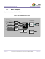
M A N G O D S P LT D. MANGO R AV E N - H X H A R DWA R E M A N UA L DSP VIDEO PROCESSING SOLUTION Release A2 This document contains proprietary information of Mango DSP Ltd. Page 1 of 40 CONFIDENTIAL Authorized Customer Use Legal Information No part of this document may be reproduced or transmitted in any form or by any means, electronic and mechanical, for any purpose, without the express written permission of Mango DSP Ltd. Copyright Copyright © 2003 Mango DSP Ltd. All rights reserved. Disclaimer Mango DSP Ltd. reserves the right to make changes in specifications at any time without notice. The information furnished by Mango DSP in this material is believed to be accurate and reliable. However, Mango DSP assumes no responsibility for its use. Trademarks Mango DSP and Raven-HX are trademarks and “Processing the Digital Vision” is a service mark of Mango DSP Ltd. Windows, the Windows logo, Windows 98/2000/Millenium/XP, and Windows NT, are either registered trademarks or trademarks of Microsoft Corporation in the United States and/or other countries. Other product and company names mentioned herein may be the trademarks of their respective owners. Linux is a registered trademark of Linus Torvalds. Patents Contact Information Mango DSP Ltd., Israel Postal: Har Hotzvim Industrial Park P.O. Box 45116 Jerusalem, 91450 Israel Tel: fax: +972-2-532 8706 +972-2-532 8705 Raven-HX H/W User's Manual Part Number 385-00021-001 Detailed Revision History Rev. Date A0 10/11/03 I. Kravitz A1 17/10/04 I. Kravitz A2 17/04/05 I. Kravitz Release A2 Author Approved Description Preliminary Release Update This document contains proprietary information of Mango DSP Ltd. Page 2 of 40 Table of Contents 1. Introduction........................................................................................................................................ 8 1.1. 2. Block Diagram........................................................................................................................................ 9 The Raven-HX Features .................................................................................................................. 10 2.1. General Specifications ......................................................................................................................... 10 2.2. Video Specifications ............................................................................................................................. 11 2.3. Audio Specifications............................................................................................................................. 11 2.4. LED Indicators..................................................................................................................................... 12 2.5. Switches and Jumpers ......................................................................................................................... 12 2.6. Connectors ............................................................................................................................................ 13 3. Connector Pinouts............................................................................................................................ 14 3.1. Audio Connector .................................................................................................................................. 14 3.2. BNC Video Connector ......................................................................................................................... 14 3.3. JTAG: DSP J5 ...................................................................................................................................... 15 3.4. Power..................................................................................................................................................... 15 3.5. JP2: General Purpose I/O Pinout ....................................................................................................... 16 4 . Description of Raven-HX Board ................................................................................................. 17 4.1. The DSP: TMS320DM642................................................................................................................... 17 4.1.1. DSP Memory .....................................................................................................................................................20 4.1.1.1. L1P Description........................................................................................................................................20 4.1.1.2. L1D Description.......................................................................................................................................20 4.1.2. Memory Map .....................................................................................................................................................21 4.1.3. External memory Interface ................................................................................................................................23 4.1.4. Boot Modes And Configuration.........................................................................................................................24 4.2. 4.2.1. TMS320DM642 Boot and Device Configuration............................................................................... 24 Peripheral Selection At Device Reset ................................................................................................................26 4.2.2. Peripheral Selection After Device Reset............................................................................................................26 4.2.3. Video Ports ........................................................................................................................................................28 4.2.3.1. Video Capture Mode ................................................................................................................................28 4.2.3.2. Video Display Mode ................................................................................................................................28 4.2.3.3. TSI Capture Mode ....................................................................................................................................29 4.2.4. Video Port Architecture .....................................................................................................................................29 4.2.5. Raven-HX Video Port Board Settings ...............................................................................................................31 4.2.6. General Purpose Input/Output (GPIO) ..............................................................................................................31 Release A2 This document contains proprietary information of Mango DSP Ltd. Page 3 of 40 4.2.7. 4.2.8. Multichannel Buffered Serial Port (McBSP) .....................................................................................................32 Multichannel Audio Serial Port (McASP) .........................................................................................................33 4.3. SDRAM ................................................................................................................................................. 33 4.4. Flash Memory....................................................................................................................................... 34 4.5. Video...................................................................................................................................................... 34 4.5.1. 4.5.2. 4.5.3. 4.6. Input Connector .................................................................................................................................................34 Video Input Ports ...............................................................................................................................................34 Phillips SAA7114 Video Decoder .....................................................................................................................34 Audio ..................................................................................................................................................... 35 4.6.1. 4.6.2. Input Connector .................................................................................................................................................35 Audio A/D .........................................................................................................................................................35 4.6.3. Audio Clocks .....................................................................................................................................................35 4.7. The Board: Raven-HX Factor............................................................................................................. 35 4.8. Ethernet................................................................................................................................................. 35 4.9. Power Supplies ..................................................................................................................................... 36 4.9.1. 4.9.2. Power-On Reset .................................................................................................................................................36 Switches.............................................................................................................................................................36 4.10. Indicators .............................................................................................................................................. 37 4.11. Clocks .................................................................................................................................................... 37 4.12. JTAG Connectors ................................................................................................................................ 38 4.12.1. 4.12.2. 4.13. 5. DSP JTAG: J5...............................................................................................................................................38 Ethernet JTAG: J15.......................................................................................................................................38 JP2: I/O Connector ............................................................................................................................. 38 Appendix A: Board Layout .............................................................................................................. 39 5.1. Release A2 Layout ................................................................................................................................................... 39 This document contains proprietary information of Mango DSP Ltd. Page 4 of 40 List of Figures FIGURE 1: BLOCK DIAGRAM OF RAVEN-HX BOARD ...................................................................................................................9 FIGURE 2: DSP INTERCONNECTIONS ...........................................................................................................................................17 FIGURE 3: VIDEO PORT BLOCK DIAGRAM ..................................................................................................................................30 FIGURE 4: THE RAVEN-HX BOARD—CONNECTOR SIDE ............................................................................................................39 FIGURE 5: THE RAVEN-HX BOARD – REVERSE SIDE..................................................................................................................40 List of Tables TABLE 1: RAVEN-HX SPECIFICATIONS .....................................................................................................................................10 TABLE 2: VIDEO SPECIFICATION ................................................................................................................................................11 TABLE 3: AUDIO SPECIFICATION ................................................................................................................................................11 TABLE 4: LED INDICATORS ........................................................................................................................................................12 TABLE 5: SWITCHES AND JUMPERS.............................................................................................................................................12 TABLE 6: RAVEN-HX CONNECTORS ...........................................................................................................................................13 TABLE 7: J4 AUDIO CONNECTOR ................................................................................................................................................14 TABLE 8: SMC VIDEO CONNECTORS..........................................................................................................................................14 TABLE 9: J5 JTAG DSP CONNECTOR PIN OUTS .........................................................................................................................15 TABLE 10: JP2 CONNECTOR PINOUT ..........................................................................................................................................16 TABLE 11: DSP MEMORY MAP SUMMARY.................................................................................................................................21 TABLE 12: EMIF SIGNAL DESCRIPTION .....................................................................................................................................23 TABLE 13: DM642 DEVICE CONFIGURATION PINS .....................................................................................................................25 TABLE 14: DM642 HPI, PCI, EMAC, MDIO AND GPIO SELECTION ........................................................................................26 TABLE 15: PERIPHERAL CONFIGURATION REGISTER SELECTION................................................................................................27 TABLE 16: PLL MULTIPLY FACTORS..........................................................................................................................................37 TABLE 17: PLL RESISTOR OPTIONS ...........................................................................................................................................38 Release A2 This document contains proprietary information of Mango DSP Ltd. Page 5 of 40 Abbreviation List The following terms and abbreviations are used throughout the document. A/D Analog to Digital Converter D/A Digital to Analog Converter DSP Digital Signal Processor EDMA Enhanced Direct Memory Access EMIF External Memory Interface FPGA Field Programmable Gate Array GPIO General Purpose I/O HPI Host Port Interface JTAG Joint Test Action Group L1P Level-one Program Cache L1D Level-one Data Cache McASP Multi-channeled Audio Serial Port McBSP Multi-channeled Buffered Serial Port PCM Pulse Coded Modulation PMC PCI Mezzanine Card SDRAM Synchronous Dynamic RAM SPI Serial Peripheral Interface TDM Time Domain Multiplexed Release A2 This document contains proprietary information of Mango DSP Ltd. Page 6 of 40 Related Documentation 1. PCI Local Bus Specification Revision 2.2. 2. TMS320DM642 Data Manual SPRS200B 3. TMS320DM642 Technical Overview SPRU615 Application Report 4. TMS320C6000 Peripherals Reference Guide. 5. Micron SDRAM MT48LC4M32B2 Datasheet. 6. Philips Semiconductor SAA7114H datasheet. 7. Philips Semiconductor SAA7121 datasheet 8. Texas Instrument PCM3010 A/D datasheet. Release A2 This document contains proprietary information of Mango DSP Ltd. Page 7 of 40 Hardware Specification 385-00021-001 1. Raven-HX H/W User's Manual Introduction This document describes the hardware implementation of the Raven-HX™ board. The Mango RavenHX is a custom designed IP Node platform. Designed with one TI DM642 Digital Media Processors, the Mango Raven-HX constitutes a compelling video processing solution. Combining video and audio input and outputs and DSP processing, the Raven-HX offers a programmable solution for even the most demanding audio/video imaging applications. Ease of design is further enhanced with the ready for use Mango video libraries such as the JPEG Encoding libraries. These video libraries include a comprehensive set of video compression encoders and decoders as well as many imaging functions. This document defines the functional hardware specifications for the Mango Raven-HX board. The Raven-HX inputs one composite video channel through a BNC connector, or one S-Video channel through two BNC type connectors. The video input channel is input to one Phillips Video A/D device. The A/D decodes the channel and transmits the 8-bit data stream to a DM642 DSP video port. The second video port of the A/D outputs a video data stream to a Philips SAA7121 video D/A. The Video signal is then transmitted through a BNC connector. One audio stereo channel is input to the board via a 3.5 mm audio connector. One audio stereo channel is output from the board via a 3.5 mm audio connector. The audio input and output are transmitted to a 24-bit stereo audio Codec. The audio Codec which is controlled by the DSP, samples the inputs, and outputs a serial stream to the DSPs McBSP serial port for processing. The DSP handles the synchronization of the audio and video data. The Raven-HX board connects to a network through the Ethernet media access controller (EMAC) in the DSP. The Raven-HX board contains support for one 10/100 Mb/s Ethernet terminal. The DSP has a 64-bit 133 MHz External Memory Interface (EMIF) bus that connects to 32 Mbytes of SDRAM. The 64-bit wide SDRAM bus allows for data transfer at over 1 gigabyte per second. In addition, the DSP has 4 MByte of Flash memory for booting and program storage. Release A2 This document contains proprietary information of Mango DSP Ltd. Page 8 of 40 Hardware Specification 385-00021-001 1.1. Raven-HX H/W User's Manual Block Diagram Figure 1 is a block diagram of the Raven-HX board. Figure 1: Block Diagram of Raven-HX Board DUAL BNC RAVEN-HX VIDEO IN Y VIDEO IN C VIDEO A/D 8 Bit BNC VIDEO OUTPUT VIDEO D/A VP1 8 Bit VP2 M c B S P 3.5 mm AUDIO IN LEFT AUDIO IN RIGHT AUDIO OUT LEFT AUDIO OUT RIGHT AUDIO CODEC E M A C AUDIO PCM 8 Bit FLASH DSP DM642 EMIF PHY G P I O 133 MHz 64 BITS SDRAM POWER Release A2 RJ45 This document contains proprietary information of Mango DSP Ltd. 6V Page 9 of 40 Hardware Specification 385-00021-001 2. 2.1. Raven-HX H/W User's Manual The Raven-HX Features General Specifications Table 1: Raven-HX Specifications Release A2 Characteristics Specifications Board Form Factor Custom DSP One TI TMS320DM642 SDRAM 32 MByte Video Input 1 Composite or 1 S-Video Input Video Output 1 Composite or 1 S-Video Output Audio Input 1 Stereo Input Audio Output 1 Stereo Output I/O (to internal connector) 5 GPIO signals plus 4 Timer Signals Power requirements +6VDC @ 1.0 Amp Operating Temperature 0ºC - 50ºC Storage Temperature -40ºC to 85ºC Relative Humidity 5% to 90% (non-condensing) Dimensions: Length Width 3.8 inches 3.2 inches This document contains proprietary information of Mango DSP Ltd. Page 10 of 40 Hardware Specification 385-00021-001 2.2. Raven-HX H/W User's Manual Video Specifications Table 2: Video Specification 2.3. Characteristics Specifications Video Signal Standard EIA RS-170, NTSC, PAL, ITU-601. Bandwidth 7 MHz at -3 dB Horizontal Resolution 400 lines or more Linearity 10 gray scale or better Composite Input 1.0Vp-p, 75 ohm negative sync Level Control Automatic Gain Control (AGC) Outputs 1.0vp-p, 75 ohm negative sync Audio Specifications Table 3: Audio Specification Release A2 Characteristics Specifications Number of Channels One Stereo Input, one stereo output Input Level 1 V RMS Input Impedance 20K ohm Output Level 1 V RMS (5K ohm load) Bandwidth 30 Hz to 10 KHz Signal-to-Noise Ratio 96 dB typical Dynamic Range 72 dB Total Harmonic Distortion - 96 dB typical Sampling Frequency 48 KHz This document contains proprietary information of Mango DSP Ltd. Page 11 of 40 Hardware Specification 385-00021-001 2.4. Raven-HX H/W User's Manual LED Indicators Table 4: LED Indicators 2.5. Characteristics Specifications DS1A Ethernet 1 Status DS1B General Purpose LED on DSP Switches and Jumpers Table 5: Switches and Jumpers Release A2 Connector Description SW1 Power On Reset Switch JP1 Boundary Scan Selector This document contains proprietary information of Mango DSP Ltd. Page 12 of 40 Hardware Specification 385-00021-001 2.6. Raven-HX H/W User's Manual Connectors Table 6: Raven-HX Connectors Release A2 Connector Description Manufacturer Part # J8 Video Inputs Y and C Bomar 364A2795 J16 Composite Video Output Chin Nan 13-60-6-DGN/Z J16 Optional S-Video Output Chant 607A-04PTCR003 J11 Audio Input Kycon ST-3150-3C J12 Audio Output Kycon ST-3150-3C J5 DSP JTAG Connector Samtec TSM-105-01-T-DV J10 Power connector Kycon KLD-0202-AC JP2 General Purpose I/O Samtec TSM-108-01-T-DV JP1 DSP Boundary Scan Select Samtec TSM-102-01-T-DV J15 Ethernet JTAG Samtec TSM-105-01-T-DV J6 RJ45 Ethernet Molex 43860-0010 This document contains proprietary information of Mango DSP Ltd. Page 13 of 40 Hardware Specification 385-00021-001 3. 3.1. Raven-HX H/W User's Manual Connector Pinouts Audio Connector Table 7: J4 Audio Connector 3.2. Connector Description J11 Audio Input J12 Audio Output BNC Video Connector Table 8: SMC Video Connectors Release A2 Connector Description J8 Video Y and C Inputs J16 Video Output This document contains proprietary information of Mango DSP Ltd. Page 14 of 40 Hardware Specification 385-00021-001 3.3. Raven-HX H/W User's Manual JTAG: DSP J5 Table 9: J5 JTAG DSP Connector Pin outs Pin # Name Dir. Pin # Name 1 TMS I 6 GND 2 TRST I 7 TDO 3 TDI I 8 4 GND 9 5 P3_3V 3.4. Release A2 10 Dir. Pin # Name Dir. 11 TCK I 12 GND GND 13 EMU0 I TCK_RTN 14 EMU1 I O GND Power This document contains proprietary information of Mango DSP Ltd. Page 15 of 40 Hardware Specification 385-00021-001 3.5. Raven-HX H/W User's Manual JP2: General Purpose I/O Pinout Table 10: JP2 Connector Pinout Pin # Name Dir. Pin # Name Dir. Pin # Name Dir. 1 GND 7 NC 13 GPIO BIT 1 I/O 2 3.3V PU 8 NC 14 TIMER IN 1 I 3 GND 9 GPIO BIT 3 I/O 15 GPIO BIT 0 I/O 4 GND 10 TIMER OUT 1 O 16 TIMER IN 0 I 5 GPIO BIT 8 11 GPIO BIT 2 I/O 6 GND 12 TIMER OUT 0 O Release A2 I/O This document contains proprietary information of Mango DSP Ltd. Page 16 of 40 Hardware Specification 385-00021-001 4. Raven-HX H/W User's Manual Description of Raven-HX Board 4.1. The DSP: TMS320DM642 The Raven-HX board contains one Texas Instruments TM320DM642 DSP device. The DSP receives the composite video stream at its video port. The video stream is decoded by a Philips SAA7114H A/D device. The DSP receives one stereo audio stream at the McBSP serial port. The audio A/D device receives the stereo input from the audio connector and outputs the serial data to the DSP in the Audio PCM format. The DSP transmits an audio output from the McBSP to the audio Codec which connects the audio output to the 3.5 mm audio connector. The DSP synchronizes the audio and video data. Figure 2 is a diagram of the DSP on the board. Figure 2: DSP interconnections DUAL BNC VIDEO INPUT Y VIDEO INPUT C VIDEO A/D 8 Bit VP1 BNC VIDEO OUTPUT EMAC VIDEO D/A 8 Bit AUDIO CODEC AUDIO PCM VP2 3.5 mm AUDIO IN LEFT AUDIO IN RIGHT AUDIO OUT LEFT AUDIO OUT RIGHT DSP DM642 McBSP GPIO EMIF 8 Bit FLASH Release A2 ETHERNET 133 MHz 64 BITS SDRAM This document contains proprietary information of Mango DSP Ltd. Page 17 of 40 Hardware Specification 385-00021-001 Raven-HX H/W User's Manual The TMS320DM642 fixed-point DSP has the following features: High Performance Digital Media Processor 2-, 1.67, 1.39 ns Instruction Cycle Time 500-, 600, 720 MHz Clock Rate Eight 32-Bit Instructions/Cycle 4000, 4800, 5760 MIPS VelociTI.2 Advanced Very Long Instruction Word C64x DSP Core Six ALUs (32-/40 Bit) supporting single 32-bit, dual 16-bit, quad 8-bit Arithmetic per Clock Cycle Two Multipliers Support; Four 16 X 16-Bit Multiplies or Eight 8 X 8-Bit Multiplies per Clock Cycle 64 32-Bit General Purpose Registers Instruction Set Features Byte Addressable (8-/16-/32-/64-Bit Data) 8-Bit Overflow Protection Bit-Field Extract, Set, Clear L1/L2 Memory Architecture 128K-Bit L1P Program Cache 128K-Bit L1D Data cache 2M-Bit L2 Unified Mapped RAM/Cache External Memory Interface 64-Bit EMIF Glueless Interface to SRAM and SDRAM 1024M-Byte Total Addressable External Memory Space Enhanced DMA (EDMA) Controller (64 Independent Channels) Release A2 This document contains proprietary information of Mango DSP Ltd. Page 18 of 40 Hardware Specification 385-00021-001 10/100 Mb/sec Ethernet MAC Management Data Input/Output (MDIO) Three Configurable Video Ports Glueless interface to common Video Decoder and Encoder Devices Supports Video Standards CCIR601, ITU-BT.656, BT.1120, SMPTE 125M, 260M,274M, and 296M Supports Raw Video I/O Transport Stream Interface Mode VCXO Interpolated Control Port (VIC) Raven-HX H/W User's Manual Supports Audio/Video Synchronization Host Port Interface User Configurable Bus Width (32-/16-Bit) 32-Bit 66 MHz 3.3V PCI Interface (PCI Specification 2.2) Multichannel Audio Serial Port (McASP) Eight serial Data Pins Inter-IC Sound (I2S) Bit Stream Format Integrated Digital Studio I/F Transmitter supports S/PDIF, IEC60958-1, AES-3, CP-430 Formats Two Multichannel Buffered Serial Ports I2C Bus Three 32-Bit General Purpose Timers Sixteen General Purpose I/O Pins Flexible PLL Clock Generator IEEE-1149.1 JTAG Boundary Scan Compatible 3.3V I/O, 1.4V Internal Release A2 This document contains proprietary information of Mango DSP Ltd. Page 19 of 40 Hardware Specification 385-00021-001 Raven-HX H/W User's Manual The 64-bit EMIF Bus DSP on the Raven-HX Board connects to 32 MByte of SDRAM. 4.1.1. DSP Memory The TMS320DM642 has a cache-based architecture with two-level memory architecture for program (designated L1P) and data (designated L1D). The level one program cache controller interfaces the CPU to the L1P. A 256-bit wide path is provided from the CPU to allow a continuous stream of eight 32-bit instructions. The level-one data cache controller is the interface between the CPU and the L1D. The L1D allows simultaneous access by both sides of the CPU. Both the program and data memory share the second level memory designated L2. L2 is a 1024-Byte memory space that can be configured as all memory mapped SRAM, all cache, or a combination of the two. 4.1.1.1. L1P Description The L1P on the DM642 is a 16 KByte direct-mapped cache with a 32-byte line size and 512 sets. A 32bit CPU program address is divided into three pieces to determine the physical L1P location where the data can reside. The L1P address location register is shown below. 31 … TAG 14 13 … 5 SET INDEX 4 … 0 OFFSET The five least significant bits indicate the byte offset of the program fetch packet. The next nine bits of the program address are used to indicate in which set the data can reside. The data of each address can only reside in one of 512 sets. The upper 18 bits are used as a unique tag to label what data is currently residing in that cache line. The L1P operation is controlled by the CPU control status register, the L1P flush base address register, the L1P flush word count register, and the cache configuration register. 4.1.1.2. L1D Description The L1D is a 16 KByte cache with a 64-bit wide write bus from L1D to the L2 memory. It is a twoway set associative cache with a 64-byte line size and 128 sets. A physical address from the CPU is divided into four regions to select the cache set to allocate the data in and to select the correct word from that set. The L1P address location register is shown below. 31 TAG Release A2 … 13 12 … SET INDEX 6 5 WORD … 2 1 … 0 OFFSET This document contains proprietary information of Mango DSP Ltd. Page 20 of 40 Hardware Specification 385-00021-001 Raven-HX H/W User's Manual The lower two address bits are a word offset into the address. The next four bits selects the word that contains the requested data. The next seven bits identify the set to search for the requested data. The upper 19 bits are the tag value for the address. The L1D operation is controlled by the CPU control status register, the L1D flush base address register, the L1D flush word count register, and the cache configuration register. 4.1.2. Memory Map The DM642 has one memory map which is shown in the table below. Internal memory is always located at address 0 but can be used as both program and data memory. The external memory address ranges begin at 0x8000 0000 for the EMIF. Table 11: DSP Memory Map Summary Address Range Size (Bytes) Description 0x0000 0000 – 0x0003 FFFF 256K Internal RAM (L2) 0x0004 0000 – 0x000F FFFF 768K Reserved 0x0010 0000 – 0x017F FFFF 23M Reserved 0x0180 0000 – 0x0183 FFFF 256K EMIF Registers 0x0184 0000 – 0x0187 FFFF 256K L2 Registers 0x0188 0000 – 0x018B FFFF 256K HPI Registers 0x018C 0000 – 0x018F FFFF 256K McBSP0 Registers 0x0190 0000 – 0x0193 FFFF 256K McBSP1 Registers 0x0194 0000 – 0x0197 FFFF 256K Timer 0 Registers 0x0198 0000 – 0x019B FFFF 256K Timer 1 Registers 0x019C 0000 – 0x019F FFFF 256K Interrupt Selector Registers 0x01A0 0000 – 0x01A3 FFFF 256K EDMA RAM and EDMA Registers 0x01A4 0000 – 0x01AB FFFF 512K Reserved 0x01AC 0000 – 0x01AF FFFF 256K Timer 2 Registers 0x01B0 0000 – 0x01B3 EFFF 256K - 4K GPIO Registers 0x01B3 F000 – 0x01B3 FFFF 4K Device Configuration Registers 0x01B4 0000 – 0x01B4 3FFF 16K I2CO Data and Control Registers 0x01B4 4000 – 0x01B4 BFFF 32K Reserved 0x01B5 0000 – 0x01B7 FFFF 192K Reserved 0x01B8 0000 – 0x01BB FFFF 256K Reserved 0x01BC 0000 – 0x01BF FFFF 256K Emulation Release A2 This document contains proprietary information of Mango DSP Ltd. Page 21 of 40 Hardware Specification 385-00021-001 Raven-HX H/W User's Manual Address Range Size (Bytes) Description 0x01C0 0000 – 0x01C3 FFFF 512K PCI Registers 0x01C4 0000 – 0x01C4 3FFF 16K VP0 Control 0x01C5 0000 – 0x01C4 7FFF 16K VP1 Control 0x01C4 8000 – 0x01C4 BFFF 16K VP2 Control 0x01C0 0000 – 0x01C3 FFFF 512K PCI Registers 0x01C4 0000 – 0x01C4 3FFF 16K VP0 Control 0x01C4 C000 – 0x01C4 FFFF 16K VIC Control 0x01C5 0000 – 0x01C7 FFFF 192K Reserved 0x01C8 0000 – 0x01C8 0FFF 4K EMAC Control 0x01C8 1000 – 0x01C8 2FFF 8K EMAC Wrapper 0x01C8 3000 – 0x01C8 37FF 2K EWRAP Registers 0x01C8 3800 – 0x01C8 3FFF 2K MDIO Control Registers 0x01C8 4000 – 0x01FF FFFF 3.5M Reserved 0x0200 0000 – 0x0200 0033 52 QDMA Registers 0x0200 0034 – 0x02FF FFFF 938M – 52 Reserved 0x3000 0000 – 0x33FF FFFF 64M McBSP0 Data 0x3400 0000 – 0x37FF FFFF 64M McBSP1 Data 0x3800 0000 – 0x3BFF FFFF 64M Reserved 0x3C00 0000 – 0x3C0F FFFF 1M McASP0 Data 0x3C10 0000 – 0x3FFF FFFF 64M – 1M Reserved 0x4000 0000 – 0x73FF FFFF 832M Reserved 0x7400 0000 – 0x75FF FFFF 32M VP0 Channel A Data 0x7600 0000 – 0x77FF FFFF 32M VP0 Channel B Data 0x7800 0000 – 0x79FF FFFF 32M VP1 Channel A Data 0x7A00 0000 – 0x7BFF FFFF 32M VP1 Channel B Data 0x7C00 0000 – 0x7DFF FFFF 32M VP2 Channel A Data 0x7E00 0000 – 0x7FFF FFFF 32M VP2 Channel B Data 0x8000 0000 – 0x8FFF FFFF 256M EMIF CEO 0x9000 0000 – 0x9FFF FFFF 256M EMIF CE1 0xA000 0000 – 0xAFFF FFFF 256M EMIF CE2 0xB000 0000 – 0xBFFF FFFF 256M EMIF CE3 0xC000 0000 – 0xFFFF FFFF 1G Reserved Release A2 This document contains proprietary information of Mango DSP Ltd. Page 22 of 40 Hardware Specification 385-00021-001 4.1.3. Raven-HX H/W User's Manual External memory Interface The DM642 EMIF Bus is 64-bits wide for direct connection to high speed synchronous memory. It has a maximum bus rate of 133 MHz. It has a memory controller than can interface to SDRAM, SRAM and FIFOs. The EMIF signals are described in the table below. Table 12: EMIF Signal Description PIN I/O/Z DESCRIPTION ECLKIN I EMIF A/B clock input. ECLKOUT1,2 O/Z EMIF A/B output clock at EMIF input clock frequency. ED[63:0] I/O/Z EMIF 64 bit data bus I/O. EA[22:3] O/Z EMIF external address output. CEO[0:3} O/Z Active low chip select for memory space 0 to 3. BEA[7:0] O/Z EMIF active low byte enables. ARDY I Active high asynchronous ready input to insert wait states. O/Z Multiplexed active low: output enable (asynchronous)/ RAS signal/output enable (synchronous). AOE/SDRAS/SOE ARE/SDCAS/SADS/ SRE O/Z Multiplexed active low: read strobe (asynchronous)/ CAS strobe/memory address strobe (synchronous) or read enable. AWE/SDWE/SWE O/Z Multiplexed active low: write strobe (asynchronous)/ SDRAM write enable/write enable (synchronous). SDCKE O/Z EMIFA SDRAM clock enable. SOE3 O/Z EMIF A/B synchronous memory output enable for CE3. HOLD I Active low external bus hold. HOLDA O Active low external bus hold acknowledge. BUSREQ O Active high bus request signal. PDT O/Z Peripheral device transfer data. The 64-bit EMIF bus is connected directly to the 32 MByte SDRAM. The DSP controls the operation of the SDRAM through the control signals in the table above. The DSP provides the RAS, CAS, WE, and clock to the SDRAM. Release A2 This document contains proprietary information of Mango DSP Ltd. Page 23 of 40 Hardware Specification 385-00021-001 4.1.4. Raven-HX H/W User's Manual Boot Modes And Configuration The DM642 boot mode selection and certain peripheral selections are determined at device reset. There are also some device configurations and peripheral selections that can be software configurable via the PERCFG peripheral configuration register after device reset. While the reset signal is low the DM642 is held in reset and is initialized to the configured reset state. The rising edge of reset starts the processor running with the boot configuration it is set for. The DM642 has three types of boot modes: Host Boot: If host boot is selected the CPU is stalled while the remainder of the device is released. During this period, an external host can initialize the CPU's memory space. The Raven-HX defaults to this mode by setting the PCI_EN pin to logic 1 and booting from the host computer on the PCI Bus. EMIF Boot: If EMIF boot is selected the DM642 boots from an external EPROM. The 1 KByte ROM code located at CE1 is copied to address 0 by the EDMA using the default ROM timings, while the CPU is internally stalled. After the code is transferred the CPU is released and begins to execute the program from address 0. No Boot: With no boot the CPU begins direct execution from the memory located at address 0. 4.2. TMS320DM642 Boot and Device Configuration The following configurations are latched during device reset: Input Clock Mode: The on chip PLL frequency multiplier is configured through the CLKMODE input pins. The Raven-HX is configured by resistor options for an X 12 operation. A 50 MHz external oscillator is provided for an internal operational frequency of 600 MHz and a 60 MHz oscillator is provided for a 720 MHz frequency. Boot Configuration: The pull up and pull down resistors on the EMIF address bus pins AEA[22:21], determine the boot configuration. These two pins on DSP have resistor pairs for selecting the Boot mode. They are set for the value 01 which selects Host Boot mode (based on the state of the PCI_EN bit). Device Configuration: The DM642 device configurations are determined by the TOUT1/LENDIAN, GP0(3)/PCIEEAI, and the HD5 pins, and the pull up and pull down resistors on the EMIF address bus AEA[20:19] all of which are latched at device reset. Release A2 This document contains proprietary information of Mango DSP Ltd. Page 24 of 40 Hardware Specification 385-00021-001 Raven-HX H/W User's Manual The table below describes these DM642 device configuration pins. Table 13: DM642 Device Configuration Pins Configuration Pin Pin Number TOUT1/LENDIAN B5 AEA[22:21] [U23,V24] AEA[20:19] [V25,V26] GPO[3]/PCIEEAI L5 HD5/AD5 Y1 PCI_EN; TOUT0/MAC_EN [E2,C5] Release A2 Functional Description Device Endian mode (LEND) 0: Big Endian mode 1: Little Endian mode Boot mode [1:0] 00 – No Boot 01 – HPI/PCI Boot 10 – Reserved 11 – EMIF Boot EMIFA input clock select AECLKIN_SEL = 00b: EMIF runs at AECLKIN rate AECLKIN_SEL = 01b: EMIF runs at 1/4 CPU clock rate AECLKIN_SEL = 10b: EMIF runs at 1/6 CPU clock rate AECLKIN_SEL = 11b: Reserved PCI EEPROM Auto-Initialization (PCIEEAI) 0 – PCI auto-initialization through EEPROM disabled. 1 – PCI auto-initialization through EEPROM enabled. (PCI_EN must be = to 1). HPI peripheral bus width (HPI_WIDTH) 0 – HPI operates at HPI16. (HPI bus is 16-bits wide. HD[15:0] are used, HD[31:16] in Hi-Z state) 1 – HPI operates as HPI32. (HPI bus is 32 bits wide. HP[31:0] is used). Peripheral selection 00 – HPI (default mode) 01 – EMAC and MDIO 10 – PCI 11 – Reserved This document contains proprietary information of Mango DSP Ltd. Page 25 of 40 Hardware Specification 385-00021-001 4.2.1. Raven-HX H/W User's Manual Peripheral Selection At Device Reset Some DM642 peripherals share the same pins (are internally muxed) and are mutually exclusive (HPI, GPIO [15:9], PCI and EEPROM, EMAC, MDIO and VIC). Other peripherals are always available (Timers, I2C0, GPIO[7:0]). The following table shows which of the multiplexed peripherals are selected based on the state of PCI_EN and MAC_EN at reset. Table 14: DM642 HPI, PCI, EMAC, MDIO and GPIO Selection Peripheral Selection Peripherals Selected PCI_EN Pin E2 PCI_EEAI Pin L5 HD5 PinY1 MAC_EN Pin C5 HPI Data Lower HPI Upper 0 0 0 0 √ Hi-Z Disabled Disabled Disabled √ 0 0 0 1 √ Hi-Z Disabled Disabled √ √ 0 0 1 0 √ √ Disabled Disabled Disabled √ 0 0 1 1 Disabled Disabled Disabled √ √ 1 1 X X Disabled √ Disabled Disabled 32-Bit PCI EEPROM √ EMAC MDIO GPIO [15:9] On Raven-HX board the PCI_EN is pulled down, the PCI_EEAI pin is left open, and the MAC_EN and HD5 are pulled up to enable the EMAC Ethernet and to select GPIO pins 0 to 15. 4.2.2. Peripheral Selection After Device Reset After device reset certain peripherals must be configured by writing to designated registers. They are the peripheral configuration register (PERCFG), the device status register (DEVSTAT), and the JTAG identification register (JTAGID). Release A2 This document contains proprietary information of Mango DSP Ltd. Page 26 of 40 Hardware Specification 385-00021-001 Raven-HX H/W User's Manual The table below describes the Peripheral Configuration Register (PERCFG) Selection Bits. Table 15: Peripheral Configuration Register Selection BIT NAME DESCRIPTION 31:17:00 Reserved 6 5 4 3 2 1 0 Release A2 Reserved. Read only, writes have no effect. Video Port 2 (VP2) Enable bit. VP2EN 0 = VP2 is disabled (default). 1 = VP2 is enabled. Video Port 1 (VP1) Enable bit. VP1EN 0 = VP1 is disabled (default). 1 = VP1 is enabled. Video Port 0 (VP0) Enable bit. VP0EN 0 = VP0 is disabled (default). 1 = VP0 is enabled. Inter-IC 0 (I2C0) Enable bit. I2COEN 0 = I2C0 is disabled (default). 1 = I2C0 is enabled. Video Port 1(VP1) lower Data vs. McBSP1 Enable bit. 0 = VP1 lower data pins enabled (if VP1EN = 1), McBSP1EN McBSP1 is disabled; VP1 upper data bits are Dependent on McASP0EN and VP1EN bits. 1 = McBSP1 is enabled, VP1 lower data pins disabled. Video Port 0 (VP0) lower Data vs. McBSP0 Enable bit. 0 = VP0 lower data pins enabled (if VP0EN = 1), McBSP0EN McBSP0 is disabled; VP0 upper data bits are Dependent on McASP0EN and VP0EN bits. 1 = McBSP0 is enabled, VP0 lower data pins disabled. McASP0 vs. VP0/VP1 upper data pins select bit. 0 = McASP0 is disabled; VP0 & VP1 upper data pins enabled. VP0 & VP1 lower data pins are McASP0EN Dependent on McBSP0/1EN & VP0/1En bits. 1 = McASP0 is enabled. VP0 & VP1 upper data bits are disabled; VP0 & VP1 lower data bits are Dependent on McBSP0/1EN & VP0/1EN bits. This document contains proprietary information of Mango DSP Ltd. Page 27 of 40 Hardware Specification 385-00021-001 4.2.3. Raven-HX H/W User's Manual Video Ports The DM642 device has three configurable video port peripherals (VP0, VP1, and VP2). These video port peripherals provide a direct interface to common video decoders and encoders such as the Philips SAA7114H A/D on the Raven-HX board. All three video ports have the capability to operate as a video capture port, a video display port, or a transport stream interface (TSI) capture port. The DM642 video port supports multiple resolutions and video standards (CCIR601, ITU-BT.656, BT.1120, SMPTE, 125M, 260M, 274M, and 296M). 4.2.3.1. Video Capture Mode The video port provides the following functions when it is operating in the video capture mode. Capture Rate up to 80 MHz Two channels of 8/10-bit digital video input from a digital or analog (through a video A/D decoder) camera. Digital video input is in YCbCr 4:2:2 formats with 8 or 10 bit resolution multiplexed in ITU-R BT.656 format. One channel of Y/C 16/20-bit digital video in YCbCr 4:2:2 formats on separate Y and Cb/Cr inputs. YCbCr 4:2:2 to YCbCr 4:2:0 horizontal conversions and half scaling in 8-bit 4:2:2 modes. Direct interface for two channels of up to 10-bit or one channel of up to 20-bit raw video from A/D converters. 4.2.3.2. Video Display Mode The video port provides the following functions when it is operating in the video display mode. Display rate up to 110 MHz One channel of continuous digital video output. Digital video output is YCbCr 4:2:2 with 8/10bit resolution multiplexed in ITU-R BT.656 format. One channel Y/C 16/20-bit digital video output in YCbCr 4:2:2 formats on separate Y and Cb/Cr outputs. YCbCr 4:2:0 to 4:2:2 horizontal Conversions. Programmable clipping One channel of raw data output up to 20-bits. Two channel synchronized raw data output. Sync to external video controller Release A2 This document contains proprietary information of Mango DSP Ltd. Page 28 of 40 Hardware Specification 385-00021-001 Raven-HX H/W User's Manual 4.2.3.3. TSI Capture Mode The video port provides the following functions when it is operating in the TSI Capture mode. Transport Stream Interface (TSI) from a front end device such as a demodulator or forward error correction device in 8-bit parallel format at up to 30 Mbytes per second 4.2.4. Video Port Architecture A high level block diagram of the video port architecture is shown below. Release A2 This document contains proprietary information of Mango DSP Ltd. Page 29 of 40 Hardware Specification 385-00021-001 Raven-HX H/W User's Manual Figure 3: Video Port Block Diagram VBUS CHA_VBUSP 32 VCLK1 VCLK2 VCTL1 VCTL2 VCTL3 64 Timing and Control Logic Memory Mapped Registers DMA Interface 64 BT.656 Capture Pipeline Y/C Video Capture Pipeline VDIN[19:0] 20 Raw Video Capture Pipeline TCI Capture Pipeline 10 20 20 Capture Display Buffer (2560 Bytes) 10 BT.656 Display Pipeline 20 Y/C Video Display Pipeline 20 VDOUT[19:0] Raw Video Display Pipeline 20 8 Channel A BT.656 Capture Pipeline 10 Y/C Video Capture Pipeline 10 10 Raw Video Display Pipeline 10 10 Capture Display Buffer (2560 Bytes) 64 Channel B DMA Interface 64 CHA_VBUSP Each video port consists of two channels A and B with a 5120-byte capture or display buffer that can be split between the two channels. Both channels are always configured for either capture or display only. Separate data pipelines control the formatting of capture or display data for each of the BT.656, Y/C, raw video and TSI modes. For capture operation, the port may operate as two 8/10-bit channels of BT.656 or raw video capture, or as a single channel of 8/10-bit BT.656, 8/10-bit raw video, 16/20-bit Y/C video, 16/20-bit raw video, or 8-bit TSI. For display operation, the port may operate as a single channel of 8/10-bit BT.656 display, or as a single channel of 8/10-bit BT.656, 8/10-bit raw video, 16/20-bit Y/C video, or 16/20-bit raw video display. Release A2 This document contains proprietary information of Mango DSP Ltd. Page 30 of 40 Hardware Specification 385-00021-001 Raven-HX H/W User's Manual It may also operate in a two channel 8/10-bit raw mode in which the two channels are locked to the same timing. Channel B is not used during single channel operation. 4.2.5. Raven-HX Video Port Board Settings The Raven-HX board is designed such that one input and one output channel of video are processed by the DSP. One composite video channel or one S-Video channel is input into the video A/D SA7114H device. The video A/D decodes the video stream, and outputs the video data to video port 1 of the DSP. The DSP can process one video channel at full D1 resolution. Video port 0 of each DSP is configured as the McBSP. The McBSP of the DSP receives the audio stereo data to/from a TI PCM3010DBA/D device which is driven as a serial PCM data stream. 4.2.6. General Purpose Input/Output (GPIO) The GPIO peripheral provides sixteen dedicated general purpose pins that can be configured as either inputs or outputs. When configured as an output, the user can write to an internal register to control the state driven on the output pin. When configured as an input, the user detects the state of the input by reading the state of an internal register. GPIO bits 1 and 2 are multiplexed with CLKOUT4 and CLKOUT6 respectively. These pins are software configurable. To use these pins as GPIO pins the GPxEN bits in the GPIO Enable Register and the GPxDIR bits in the GPIO Direction Register must be properly configured. If GPxEN is set high then GPx pin is enabled. If GPxDIR is set high then the GPx pin is an output. If it is low then the GPx pin is an input. GPIO bit 3 is multiplexed with the PCI EEPROM auto-initialization bit. Since the PCI enable bit (PCI_EN = 1) is set then this bit is not a general purpose bit. This bit establishes whether the PCI autoinitialization EEPROM is used. If the bit is set high the PCI auto-init is through the EEPROM. If the bit is clear then the PCI auto-init through the EEPROM is disabled. This is the default setting. GPIO bits 4, 5, 6 and 7 are multiplexed with external interrupts EXT_INT4, 5, 6 and 7 respectively. When these pins function as external interrupts (by selecting the corresponding interrupt enable register bit IER[7:4]), they are edge driven interrupt inputs and the polarity can be independently selected via the interrupt polarity register bits EXTPOL[3:0]. GPIO bit 8 is multiplexed with PCI66. When PCI_EN is set high then this bit can select the operating frequency of the PCI bus. If the bit is set then the PCI bus operates at 66 MHz (default). If the bit is cleared then the PCI bus operates at 33 MHz. This bit is pulled up high on the board by jumper JP2 to ensure 33 MHz PCI bus operation. Five GPIO bits from the DSP are connected to a 16-pin connector for general purpose I/O connector (see Table 10 above). Release A2 This document contains proprietary information of Mango DSP Ltd. Page 31 of 40 Hardware Specification 385-00021-001 4.2.7. Raven-HX H/W User's Manual Multichannel Buffered Serial Port (McBSP) The multi-channel buffered serial port (McBSP) is based on the standard serial port interface. The McBSP provides the following functions: Full-duplex communication Double buffered data registers for a continuous data stream Independent framing and clocking for receive and transmit Direct interface to industry standard codecs, analog interface chips, and other serially connected A/D and D/A devices External shift clock or an internal programmable frequency shift clock for data transfer Auto-buffering capability through the 5-channel DMA controller. The McBSP consists of a data path and a control path which connect to external devices. Data is communicated via a Receive clock (CLKR) and a transmit clock (CLKX). Control information (clocking and frame synchronization) is transmitted with four other pins: Received serial data (DR), Transmitted serial data (DX), Receive frame synchronization (FSR), and Transmit frame synchronization (FSX). Data is sent to devices interfacing to the McBSP via the DX and DR pins. Control information is sent via the CLKX CLKR, FSX, and FSR pins. The DM642 DSP communicates to the McBSP via 32-bit wide control registers accessible via the internal peripheral bus. Either the CPU or the DMA/EDMA controller reads the received data fro the Data receive register (DRR) and writes the data to be transmitted to the Data Transmit Register (DXR). Data in the DXR is shifted out by the DX pin via the Transmit Shift Register (XSR). Data received on the DR pin is shifted into the RSR and copied into the Receive Buffer Register (RBR). RBR data is copied to the DRR which can be read by the CPU or the DMA/EDMA. The Raven-HX utilizes one of the two serial ports of the DSP (McBSP0) for the stereo audio input and output. McBSP0 is multiplexed with pins from the DSPs Video Port 0. The A/D device converts the stereo audio input and output channels into a digital serial data format. Release A2 This document contains proprietary information of Mango DSP Ltd. Page 32 of 40 Hardware Specification 385-00021-001 4.2.8. Raven-HX H/W User's Manual Multichannel Audio Serial Port (McASP) The Multichannel Audio Serial Port (McASP) operates as a general purpose audio serial port. The McASP consists of independent transmit and receive sections that have separate master clocks, bit clocks, and frame syncs with different transmit modes and bit stream formats. The transmit and receive sections may operate independently or synchronized. In addition, all the McASP pins can be configured as general purpose I/O (GPIO) pins. The McASP is designed to connect to audio D/A converters, codecs, digital audio interface (DIR) receivers, and SPDIF transmit physical layer components. The McASP is not used on the Raven-HX. 4.3. SDRAM The Raven-HX provides 32 MBytes of SDRAM for the DSP. The SDRAM Bus is unbuffered from the DM642 DSP and is composed of two 4M X 32-Bit SDRAM devices and configured as 4MBytes x 64Bit words. The SDRAM consists of two 1 Meg X 4 banks X 32-Bit 133 MHz SDRAM chips, MT48LC4M32B2-FC-7, by Micron. The device has the following features: Fully Synchronous; all signals registered on positive edge of system clock Internal pipelined operation; column address can be changed every clock cycle. Internal banks for hiding row access/precharge Programmable burst lengths: 1, 2, 4, 8 or full page Auto Precharge, includes Concurrent Auto Precharge, and Auto Refresh Modes Self refresh Modes 64 ms, 4.096-cycle refresh (15.6 µs/row) Supports CAS Latency of 1, 2, and 3 Release A2 This document contains proprietary information of Mango DSP Ltd. Page 33 of 40 Hardware Specification 385-00021-001 4.4. Raven-HX H/W User's Manual Flash Memory The Raven-HX provides 4 MBytes of FLASH memory for the DSP. The DSP connects bits 0 – 7 of the EMIF Bus to the data bits of the Flash memory. Address bits 3 – 22 of the DSP are connected to the Flash address bits A0 – A19 for 1 MByte of memory. GPIO bits 12 and 13 are connected to the Flash memory A20 and A21 address for page mode access to the full 4 Mbytes of the Flash memory. The Flash used is the Intel StrataFlash RC28F320J3A-110. 4.5. 4.5.1. Video Input Connector The Raven-HX board inputs the video input channel on a Bomar Dual BNC connector. 4.5.2. Video Input Ports The Raven-HX supports one video input which is transmitted to the board with a 75 ohm coax cable to a BNC connector. The two BNC inputs support one composite video channels or one S-Video channel. The A/D device receives the composite video channel. The video input is captured and transmitted to the DSP for further processing. . 4.5.3. Phillips SAA7114 Video Decoder The PAL/NTSC/SECAM video decoder IC, Philips SA7114H is a video capture device which includes an adaptive PAL/NTSC comb filter, VBI-data slicer, anti-aliasing filter, 9-bit A/D converters, and Automatic Gain Control (AGC). The SA7114H accepts analog inputs CVBS or S-Video (Y/C) from a TV or VCR source and supports 8 or 16-bit wide output data with auxiliary reference data for interfacing to VGA controllers. The device is programmed through the I2C bus with full write and read capability for all programming registers with a bit rate up to 400 Kbits per second. Release A2 This document contains proprietary information of Mango DSP Ltd. Page 34 of 40 Hardware Specification 385-00021-001 4.6. 4.6.1. Raven-HX H/W User's Manual Audio Input Connector The Raven-HX board receives one audio stereo channels and transmits one audio stereo output on two stereo 3.5 mm audio connectors. 4.6.2. Audio A/D The Raven-HX board receives one stereo audio channel on the 3.5 mm audio connector and transmits one stereo channel on a 3.5 mm connector. The audio codec IC, Texas Instrument PCM3010, includes the 24-Bit Delta-Sigma A/D and D/A, and the Antialiasing Filter. Please consult the Texas Instrument PCM3010 data sheet for programming information. 4.6.3. Audio Clocks The CODEC requires 3 clocks, LRCK= sample rate, SCKI = M x LRCK, and BCK = 2 x Bit Rate. M is a multiplier with one of the following values, 256, 384, 512, and 768. The Bit Rate is dependent on the A/D – D/A width, either 16 or 24 bits per sample. As supplied, there is a 24.576MHz clock connected to SCKI through a zero OHM resister, R54. The user needs to supply the required clock values. 4.7. The Board: Raven-HX Factor 4.8. Ethernet The Raven-HX board has one Ethernet channels one for the DSP. The Ethernet media access controller (EMAC) on the DSP provides an interface between the DM642 DSP core processor and the network. The DM642 EMAC support both 10Base-T and 100Base-TX, or 10 Mbits/sec and 100 Mbits/sec in either half duplex or full duplex. The Raven-HX board provides the PHY layer and the RJ45 connectors externally. Release A2 This document contains proprietary information of Mango DSP Ltd. Page 35 of 40 Hardware Specification 385-00021-001 4.9. Raven-HX H/W User's Manual Power Supplies The Raven-HX board receives its power from a power connector. The power connector provides a 6V supply to the card. The board is shipped with an external AC to DC switching power supply. This external supply operates over a range of 90VAC to 230VAC input and outputs the 6V required by the board. The 6V is input to the J10 power connector where it passes through a protection diode. The voltage is input to a regulator to create the 5V needed for the audio circuit. The board uses DC to DC switching power supplies to create all the voltages on the board. The board uses 3.3V for most of the devices on board. In addition the DSP requires 1.4V for its core voltage. 4.9.1. Power-On Reset A Maxim reset device MAX6412 is provided on the board to perform a power on reset function. The MAX6412 is a microprocessor voltage monitor with a manual reset pin. The supervisor chip asserts a reset signal whenever the supply voltage falls below its threshold voltage. The reset output timeout period is externally set by a capacitor. There is a pushbutton reset switch, SW1, which when activated will assert reset. The reset output is driven to the DSP. The reset signal is driven on the board by two FET drivers. 4.9.2. Switches Switches on the board include: Power On Reset – momentary push-button switch [SW1] JP1 is a 4-pin header which is used to select the DSPs functional mode of operation. The board is shipped without any jumpers. This default mode is the Emulation/Normal Mode of the device. In order to run the JTAG Boundary Scan function on the DSP a jumper must be placed between pins 1 and 2 and between pins 3 and 4. Pin 4 is the DSPs EMU0 pin while pin 2 is EMU1. The jumpers pull down EMU0 and EMU1 placing the DSP in the Boundary Scan/Normal mode of operation. J5 is a 14-pin header for the DSPs JTAG. J15 is the JTAG connector for performing Boundary Scan on the Ethernet PHY device. Release A2 This document contains proprietary information of Mango DSP Ltd. Page 36 of 40 Hardware Specification 385-00021-001 4.10. Raven-HX H/W User's Manual Indicators LED indicators on the board are included for software convenience and for a power on condition. The power on indicator DS1 is connected to the 3.3V supply, DS2 is connected to the 5V supply. The Ethernet connector has one LED DS1A associated with it. The LED indicates the receiver status. The DSP has one LED indicator DS1B connected to the timer output signal TOUT1. 4.11. Clocks The Raven-HX provides two oscillator devices on board for separate control of the speeds of EMIF and the system clock of the DSP. The oscillator used for EMIF is a 133 MHz oscillator. The oscillator output is sent to an ICS8302 Low Skew Clock Buffer. The output of the clock buffer is driven to the clock input of the EMIF of the DSP. The second oscillator is the 50 MHz system clock. This oscillator is also driven to an ICS8302 clock buffer and then driven to the DSP. The 50 MHz clock is transmitted to the PLL CLKIN input of the DSP. The PLL multiplies the clock frequency to generate the internal CPU clock. The DSP is configured by pins CLKMODE0 and CLKMODE1 for the value 10. The DSP has internal pull downs on these inputs so only CLKMODE1 has to be pulled up. This is done by resistor R265. This mode sets the internal PLL multiply factor to be X 12 for an internal operational frequency of 600 MHz. For the 720 MHz DM642 option a 60 MHz oscillator is used. The following tables show the CLKMODE0 and CLKMODE1 PLL Multiply Factor options and the corresponding pull up resistors for the DSP to set the DM642 device to one of the valid PLL multiply clock modes. Table 16: PLL Multiply Factors CLKMODE1 Release A2 CLOCKMODE0 CLKMODE (PLL Multiply Factors) CLK Range MHz. CPU Clock MHz. 0 0 Bypass (x1) 30-75 30–75 0 1 x6 30-75 180–450 1 0 x12 30-50 360–600 1 1 Reserved This document contains proprietary information of Mango DSP Ltd. Page 37 of 40 Hardware Specification 385-00021-001 Raven-HX H/W User's Manual Table 17: PLL Resistor Options DSP1 CLKMODE0 R266 CLKMODE1 R265 The third oscillator is the 27 MHz video clock. This oscillator is driven to the SA7114H video A/D device. 4.12. JTAG Connectors The Raven-HX contains a JTAG Header for emulation of the DSP. DSP JTAG connector J5 is the JTAG header for the DSP emulator chain. 4.12.1. DSP JTAG: J5 The J5 connector is a Samtec part number TSM-107-01-T-DV which is the standard 14 pin header that mates with the emulator connector. The TDI signal is driven to the TDI signal of the DSP. The TDO of the DSP is driven to the J5 DSP JTAG header. 4.12.2. Ethernet JTAG: J15 The J15 connector is a Samtec part number TSM-105-01-T-DV which is a 10 pin header. J15 is used for boundary scan of the Ethernet PHY device LXT972A. 4.13. JP2: I/O Connector The Raven-HX contains an internal I/O connector JP2. This connector contains five GPIO signals and four timer signals for general purpose usage. JP2 does not go to the chassis and is currently for internal use only. Release A2 This document contains proprietary information of Mango DSP Ltd. Page 38 of 40 Hardware Specification 385-00021-001 5. 5.1. Raven-HX H/W User's Manual Appendix A: Board Layout Layout Figure 4: The Raven-HX board—Connector Side Release A2 This document contains proprietary information of Mango DSP Ltd. Page 39 of 40 Hardware Specification 385-00021-001 Raven-HX H/W User's Manual Figure 5: The Raven-HX Board – Reverse Side Release A2 This document contains proprietary information of Mango DSP Ltd. Page 40 of 40