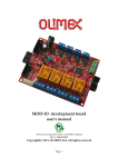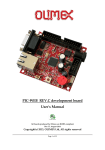
1
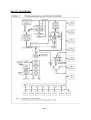
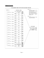
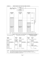
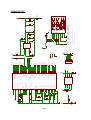
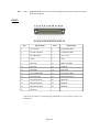
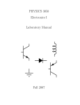
PIC-MICRO-WEB development board User's manual Rev. E, January 2014 Copyright(c) 2011, OLIMEX Ltd, All rights reserved Page 1 INTRODUCTION: This small and compact board will give you the opportunity to add Internet connectivity to any of your existing design or machine. Packed in compact plastic enclosure with DB25 male connector for the microcontroller ports and with the unique PoE (Power over Ethernet) feature which allows PIC-MICRO-WEB to take power by the Ethernet cable and with no need for external power supply adapter. The TCP-IP stack provided by Microchip is free of charge and royalties and allows you to do http, ftp, e-mail etc services. You can control the PIC GPIOs by web interface and to acquire and send data from external sensors to other Internet applications and clients. With 128K Flash memory for programs and 128KB Flash memory for web storage this small device have all resources usually needed for general embedded Internet applications and interface of sensors and machines to Internet. BOARD FEATURES: PIC18F67J60 microcontroller with Ethernet and 1 Mbit memory for code 1Mbit on board serial flash for web pages storage mini ICSP/ICD connector for programming with PIC-ICD2, PIC-ICD2-TINY and PIC-ICD2-POCKET. Power-Over-Ethernet support (for use with MOD-PoE power supply injector on standard LAN cables/switches) It is possible to use the board without PoE in which case DB25.pin8 (Vin) should be connected to 24-50 VDC source The board is enclosed in plastic shell DB25 parallel port 25 available signals and power supply on the DB25 connector Dimensions 50x30 mm (2 x 1.2") ELECTROSTATIC WARNING: The PIC-MICRO-WEB board is shipped in protective anti-static packaging. The board must not be subject to high electrostatic potentials. General practice for working with static sensitive devices should be applied when working with this board. BOARD USE REQUIREMENTS: Cables: 1.8 meter USB A-B cable to connect PIC-KIT3. Other cables might be required in case of other programming/debugging tools. You will also need a LAN cable. Hardware: Programmer/Debugger – PIC-KIT3 or other compatible programming/debugging tool. Page 2 MOD-PoE – module that provides Power-Over-Ethernet. If you don't want to use this module, you should apply power (24-50VDC) directly to DB25.pin8. Software: PIC-MICRO-WEB is tested with MPLAB IDE v.7.62 + MPLAB C18 C compiler. It is possible that the stack might not function properly if used with later versions of MPLAB IDE. PROCESSOR FEATURES: PIC-MICRO-WEB board use MCU PIC18F67J60 from Microchip with these features: - IEEE 802.3 compatible Ethernet Controller - Integrated MAC and 10Base-T PHY - 8-Kbyte Transmit/Receive Packet Buffer SRAM - Supports One 10Base-T Port - Programmable Automatic Retransmit on Collision - Programmable Padding and CRC Generation - Programmable Automatic Rejection of Erroneous Packets - Activity Outputs for 2 LED Indicators - Buffer: o Configurable transmit/receive buffer size o Hardware-managed circular receive FIFO o Byte-wide random and sequential access o Internal DMA for fast memory copying o Hardware assisted checksum calculation for various protocols - MAC: o Support for Unicast, Multicast and Broadcast packets o Programmable Pattern Match of up to 64 bytes within packet at userdefined offset o Programmable wake-up on multiple packet formats - PHY: o Wave shaping output filter - Selectable System Clock derived from Single 25 MHz External Source: o 2.778 to 41.667 MHz - Internal 31 kHz Oscillator - Secondary Oscillator using Timer1 @ 32 kHz - Fail-Safe Clock Monitor: o Allows for safe shutdown if oscillator stops - Two-Speed Oscillator Start-up - High-Current Sink/Source: 25 mA/25 mA on PORTB and PORTC - Five Timer modules (Timer0 to Timer4) - Four External Interrupt pins - Two Capture/Compare/PWM (CCP) modules - Three Enhanced Capture/Compare/PWM (ECCP) modules: o One, two or four PWM outputs Page 3 - - - - o Selectable polarity o Programmable dead time o Auto-shutdown and auto-restart Up to Two Master Synchronous Serial Port (MSSP) modules supporting SPI (all 4 modes) and I2C™ Master and Slave modes Up to Two Enhanced USART modules: o Supports RS-485, RS-232 and LIN 1.2 o Auto-wake-up on Start bit o Auto-Baud Detect (ABD) 10-Bit, Up to 16-Channel Analog-to-Digital Converter module (A/D): o Auto-acquisition capability o Conversion available during Sleep Dual Analog Comparators with Input Multiplexing Parallel Slave Port (PSP) module (100-pin devices only) 5.5V Tolerant Inputs (digital-only pins) Low-Power, High-Speed CMOS Flash Technology: o Self-reprogrammable under software control C compiler Optimized Architecture for Reentrant Code Power Management Features: o Run: CPU on, peripherals on o Idle: CPU off, peripherals on o Sleep: CPU off, peripherals off Priority Levels for Interrupts 8 x 8 Single-Cycle Hardware Multiplier Extended Watchdog Timer (WDT): o Programmable period from 4 ms to 134s Single-Supply 3.3V In-Circuit Serial Programming™ (ICSP™) via Two Pins In-Circuit Debug (ICD) with 3 Breakpoints via Two Pins Operating Voltage Range of 2.35V to 3.6V (3.1V to 3.6V using Ethernet module) On-Chip 2.5V Regulator Page 4 BLOCK DIAGRAM: Page 5 MEMORY MAP: Page 6 Page 7 Page 8 100nF 330 C31 RST R1 100k 3.3V 10uF/6.3V 19 C17 20 54 55 52 45 49 48 9 25 41 56 C12 100nF 26 38 57 #SS1 SCK MOSI 4 3 2 1 U2 /WP/ AT45DB011 /CS/ VCC GND SO 5 6 7 8 #SS1 SCK MISO MOSI PGC PGD C2 100nF MISO 17 16 15 14 13 12 11 8 3.3V RF1/AN6/C2OUT RF2/AN7/C1OUT RF3/AN8 RF4/AN9 RF5/AN10/CVREF RF6/AN11 RF7/#SS1 RG4/CCP5/P1D /RESET/ SCK SI PIC18F67J60 AVDD AVSS VDDPLL VSSPLL VSSTX VSSRX 2 1 64 63 62 61 60 59 58 30 29 33 34 35 36 31 32 3 4 5 6 44 43 42 37 24 23 22 21 28 27 Q4 1 2 3 4 5 6 PGD PGC 3.3V RST 10pF 10pF R2 330 LED red 3.3V VIN WU06S X1-19 P5 P6 P4 X1-18 X1-22 X1-9 X1-24 X1-11 X1-12 X1-25 X1-13 X1-23 X1-10 ICSP C18 C19 X1-17 X1-5 X1-3 32768/6pF GND P3 X1-21 X1-20 P1 P2 db25_male X1-2 X1-15 X1-4 X1-16 X1-1 X1-14 3.3V C1 100nF X1-7 X1-6 X1-8 150K C14 4.7nF R12 FB N.C. INV VIN U4 EN GND RT SW 3.3V C20 VIN TPIN- TPIN+ TPOUT- TPOUT+ 49.9/1% 10 9 7 8 3 5 6 1 4 2 L2 2x75 Ohm RJP-003TC1 PW- PW+ GND NC 2x1000pF/2KV RD+ RCT RD- TD+ TCT TD- LAN C6 D1 1N5819(smd) CL47uH/SD75 http://www.olimex.com/dev COPYRIGHT(C) 2009, Olimex Ltd. Rev. C PIC-MICRO-WEB 100nF C10 49.9/1% R6 49.9/1% R5 49.9/1% R4 100nF R11 390K ferrite bead R3 100n C11 2.2uF/50V C9 7 6 1 5 L1 BD9001FSO-8 3 2 4 8 Z1 1N4731(4.3V) VIN + R13 R20 10K 330 + 3.3V 3.3V 100nF C15 C16 100nF R15 100nF 3.3V C8 100nF 100nF C7 3.3V C13 3.3V 10 RB0/INT0/FLT0 RB1/INT1 RB2/INT2 RB3/INT3 RB4/KBI0 RB5/KBI1 RB6/KBI2/PGC RB7/KBI3/PGD RA0/LEDA/AN0 RA1/LEDB/AN1 RA2/AN2/VREFRA3/AN3/VREF+ RA4/T0CKI RA5/AN4 RC0/T1OSO/T13CKI RBIAS RC1/T1OSI/ECCP2/P2A RC2/ECCP1/P1A VDDCORE/VCAP RC3/SCK1/SCL1 RC4/SDI1/SDA1 RC5/SDO1 RC6/TX1/CK1 VDD RC7/RX1/DT1 VDD1 VDD2 RD0/P1B RD1/ECCP3/P3A RD2/CCP4/P3D VSS VSS1 RE0/P2D VSS2 RE1/P2C VSS3 RE2/P2B RE3/P3C VDDTX RE4/P3B VDDRX RE5/P1C TPOUTTPOUT+ TPINTPIN+ OSC2/CLKO OSC1/CLKI ENVREG #MCLR U1 C24 3.3V_E close 3.3V J7,8 J4,5 J6 J3 J2 J1 R10 1.8k/1% R9 4.3k/1% 1 220nF 270/1% 50 51 TPOUTTPOUT+ 53 46 47 TPINTPIN+ 2k/1% C5 GND_ GND 39 18 R14 1M 40 R7 C4 22pF Q1 25MHz 7 2 R8 C3 22pF 3.3V RST SCHEMATIC: CE220uF/10V + CE220uF/10V POWER SUPPLY CIRCUIT: PIC-MICRO-WEB takes power over Ethernet using the module MOD-PoE. Other possibility is 24-50VDC to be directly applied to DB25.pin8 if MOD-PoE is not to be used. The board power consumption depends on the applied power supply and may vary. At 24VDC the consumption is about 40 mA. RESET CIRCUIT: PIC-MICRO-WEB reset circuit is made with R20 (10k) pull-up, R13 (330Ω) and capacitor C31 (100nF). CLOCK CIRCUIT: Quartz crystal 25 MHz is connected to PIC18F67J60 pin 39 clock in (OSC1/CLKI) and pin 40 clock out (OSC2/CLKO). Quartz crystal 32.768 kHz is connected to PIC18F67J60 pin 29 (T1OSI) and pin 30 (T1OSO) and supplies the Timer1. JUMPER DESCRIPTION: 3.3V_E enables 3.3 V power supply for the PIC18F67J60 and all other devices. Default state is closed. INPUT/OUTPUT: Status red LED connected to PIC18F25J10 pin 44 (PORTB.RB4/KBI0). EXTERNAL CONNECTORS DESCRIPTION: ICSP: Pin # PGD Signal name 1 RST 2 +5V 3 GND 4 PGD 5 PGC 6 NC I/O Program Data. Serial data for programming. Page 9 PGC Input Program Clock. Clock used for transferring the serial data (output from ICSP, input for the MCU). DB25: Pin # Signal Name Pin # Signal Name 1 RA4/T0CKI 2 RA0/LEDA/AN0 3 RC2/ECCP1/P1A 4 RA2/AN2/VREF- 5 RC7/RX1/DT1 6 VCC +3.3V 7 GND 8 VIN 9 RE1/P2C 10 RD2/CCP4/P3D 11 RE3/P3C 12 RE4/P3B 13 RD0/P1B 14 RA5/AN4 15 RA1/LEDB/AIN1 16 RA3/AN3/VREF+ 17 RC6/TX1/CK1 18 RF2/AN7/C1OUT 19 RG4/CCP5/P1D 20 RB1/INT1 21 RB0/INT0/FLT0 22 RE0/P2D 23 RD1/ECCP3/P3A 24 RE2/P2B 25 RE5/P1C VIN is the pin where you should apply 24-50VDC in case you don't want to use MOD-PoE. Page 10 LAN: Pin # Signal Name Chip Side Pin # Signal Name Chip Side 1 TPOUT+ 6 TPIN- 2 TPOUT- 7 GND 3 TPIN+ 8 Not Connected (NC) 4 3.3V 9 VIN 5 Not Connected (NC) 10 GND TPOUTTPOUT+ TPINTPIN+ VIN Output Differential signal output. Output Differential signal output. Input Differential signal input. Input Differential signal input. Input Power supply for the board – over Ethernet. Page 11 AVAILABLE DEMO SOFTWARE: You could find information about PIC-MICRO-WEB board, Microchip TCP/IP stack and how to change and configure the software on Understanding PIC WEB boards here: https://www.olimex.com/Products/PIC/_resources/Understanding-PIC-WEBboards.pdf Page 12 ORDER CODE: PIC-MICRO-WEB – assembled and tested (no kit, no soldering required) How to order? You can order to us directly or by any of our distributors. Check our web page https://www.olimex.com/ for more info. All boards produced by Olimex are RoHS compliant Revision history: Board's Revision: Manual's Revision: Rev. C – created October 2009 Rev. E – edited January 2014 Fixed wrong minimum voltage required. Updated links. Formatting improvements. Page 13 Disclaimer: © 2011 Olimex Ltd. All rights reserved. Olimex®, logo and combinations thereof, are registered trademarks of Olimex Ltd. Other terms and product names may be trademarks of others. The information in this document is provided in connection with Olimex products. No license, express or implied or otherwise, to any intellectual property right is granted by this document or in connection with the sale of Olimex products. Neither the whole nor any part of the information contained in or the product described in this document may be adapted or reproduced in any material from except with the prior written permission of the copyright holder. The product described in this document is subject to continuous development and improvements. All particulars of the product and its use contained in this document are given by OLIMEX in good faith. However all warranties implied or expressed including but not limited to implied warranties of merchantability or fitness for purpose are excluded. This document is intended only to assist the reader in the use of the product. OLIMEX Ltd. shall not be liable for any loss or damage arising from the use of any information in this document or any error or omission in such information or any incorrect use of the product. Page 14