1
PALCE16V8H-15/25
Just Like a GAL® DeviceOnly Better
••
~
~.
Advanced
Micro
Devices
Advanced Micro Devices is proud to introduce the PALCE16V8, an EECMOS
PAL® device that is pin, function and fuse-map compatible with all 20-pin
GAL® devices. This kit is provided to introduce you to the many benefits of using
electrically erasable, universal architecture PAL devices. Please use the
enclosed business reply card to request additional and more detailed information.
Why do we think you will want to use the PALCE16V8?
Because ...
• it replaces up to 16 standard PAL devices,
• it consumes only half the power of those same devices,
• it is reprogram mabie within seconds,
and most importantly ...
• it is produced by AMD, the world's leading supplier of programmable
logic devices.
Give our new PALCE16V8 a try. Take a look at our data sheet and compare the
critical set-up and clock-to-output specifications to other suppliers' GAL devices.
Once you do, you will agree that the PALCE16V8 is just like a GAL device - only
better!
Andy Robin
Director of Marketing
Programmable Logic
TABLE OF CONTENTS
PALCE16V8 Data Sheet ....................................................................................... iii
PALASM 2 Software Support for the PALCE16V8 ............................................ a-1
Design a Decoder for the PALCE16V8 ................................................................. 1
About this Tutorial ................................................................................................. 2
Install the Software ................................................................................................3
Learn the Menu .....................................................................................................4
Create the Decoder Design ................................................................................... 5
Learn the Structure of the PALASM Design File ...................................... 6
Build the Declaration Segment ................................................................. 8
Build the Simulation Segment ................................................................ 15
Process the Design File ...................................................................................... 22
Autorun Compile and Simulate .............................................................. 23
View the Output Files .......................................................................................... 26
View the Compile Output Files ............................................................... 27
View the Simulation Output Files ........................................................... 28
ii
-
Advanced
Micro
Devices
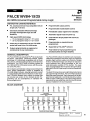
PALCE16V8H-15/25
EE CMOS Universal Programmable Array Logic
DISTINCTIVE CHARACTERISTICS
•
•
•
•
•
Pin, function and fuse-map compatible with all
20-pln GAL ® devices
Electrically erasable CMOS technology
provides reconfigurable logic and full
testability
High speed CMOS technology
15-ns propagation delay for "-15" version
25-ns propagation delay for "-25" version
Direct plug-in replacement for the PAL 16R8
series and most of the PAL 1OH8 series
Outputs programmable as registered or
combinatorial in any combination
•
•
•
•
•
•
•
•
Programmable output polarity
Programmable enable/disable control
Preloadable output registers for testability
Automatic register reset on power up
Cost-effective 20-pin plastic DIP and PLCC
packages
Programmable on standard device
programmers
Supported by PALASM ® software
Fully tested for high programming and
functional yields and high reliability
GENERAL DESCRIPTION
The PALCE16V8 is an advanced PAL® device built with
low-power, high-speed, electrically-erasable CMOS
technology. It is functionally compatible with all 20-pin
GAL devices. The macrocells provide a universal device
architecture. ThePALCE16V8 will directly replace the
PAL 16R8 and PAL 1OH8 series devices, with the exception of the PAL 16C1.
Device logic is automatically configured according to the
user's design specification. Design is simplified by
PALASM design software, allowing automatic creation
of a programming file based on Boolean or state equations. PALASM software also verifies the design and
can provide test vectors for the finished device. Programming can be accomplished on standard PAL
device programmers.
The PALCE16V8 utilizes the familiar sum-of-products
(AND/OR) architecture that allows users to implement
complex logic functions easily and efficiently. Multiple
levels of combinatorial logic can always be reduced to
sum-of-products form, taking advantage of the very
wide input gates available in PAL devices. The equations are programmed into the device through floatinggate cells in the AND logic array that can be erased electrically.
The fixed OR array allows up to eight data product terms
per output for logic functions. The su m of these products
feeds the output macrocell. Each macrocell can be programmed as registered or combinatorial with an activeHIGH or active-LOW output. The output configuration is
determined by two global bits and one local bit controlling four multiplexers in each macrocell.
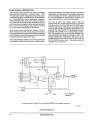
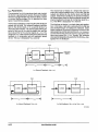
BLOCK DIAGRAM
12015-0011<
PALCE16V8 Block Diagram
Publication # 12015
Issue Date: April 1989
Rev. A
Amendment
iii
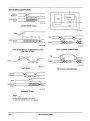
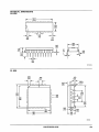
CONNECTION DIAGRAMS
DIP
ClK/lo
PLCC
VCC
11
1/0 7
12
II0s
13
1/0 5
14
1/04
15
1/0 3
Is
1/02
17
1/01
IB
1/0 0
GND
'2 '1 elK/lo Vcc
'B
OE/lg
1/0 7
GND DE/l g 1100 1/01
12015-002A
Pin Designations:
I
1/0
m:
ClK
Vee
GND =
12015-003A
Note: Pin 1 is marked for orientation
Input
InputOutput
Output Enable
Clock
Supply Voltage
Ground
ORDERING INFORMATION
Standard Products
AMD/MMI standard products are available in several packages. The order number (Valid Combination) is
formed by a combination of:
a Device Number
b. Speed/Power Option
c. Package Type
d. Operating Conditions
PAL
a.
PROGRAMMABLE
ARRAY LOGIC
CE
~
--
~
CMOS ELECTRICALLY
ERASABLE
-- L
16 V 8 H -15 P C
d. OPERATING CONDITIONS
C = Commercial (O°C to +75°C)
NUMBER OF
ARRAY INPUTS
c. PACKAGE TYPE
P = Plastic DIP, (PD 020)
J = Plastic leaded Chip Carrier,
(Pl 020)
OUTPUT TYPE
V = Versatile
NUMBER OF FLiP-FLOPS--------'
b. P O W E R - - - - - - - - - - - - -.....
H = Half Power
PERFORMANCE------------....I
-15 = 15 ns tpD
-25 = 25 ns tpD
Valid Combinations
Valid Combinations
PAlCE 16V8H-15
PC,JC
PAlCE16V8H·25
iv
The valid Combinations table lists configurations
planned to be supported in volume for this device. Con·
suit the local AMD sales office to confirm availability of
specific valid combinations, to check on newly released
combinations, and to obtain additional data on AM D's
standard military grade products.
PALCE16V8H-15/25
PIN DESCRIPTION
Symbol
Function
Type
Five Volt Power Input.
Vee
GND
Ground
ClK/Io
TTL input
Clock. If the ClK function is not used, it can used as a TTL input signal
OE/l g
TTL Input
Output Enable. If the OE function is not used, it can be used as a
TTL input signal.
I, .. Is
1/0 0 •• 1/07
TTL inputs
TTL 1/0
Input 1 through Input 8
1/0 0 through 1/07
PALCE16V8H-15/25
v
FUNCTIONAL DESCRIPTION
The PALCE16V8 is a universal PAL device. It has eight
independently configurable macrocells (MC o•• MC 7).
The macrocells can be configured as registered output,
combinatorial output, combinatorial 1/0 or dedicated input. The programming matrix implements a programmable AND logic array, which drives a fixed OR logic array. Buffers for device inputs have complementary outputs to provide user-programmable input signal polarity.
Pins 1 and 11 serve either as array inputs or as clock
(CLK) and output enable (OE) for all flip-flops.
Unused input pins should be tied directly to VCC or
GND. Product terms with all bits unprogrammed (disconnected) assume the logical HIGH state and product
terms with both true and complement of any input signal
connected assume a logical LOW state.
The programmable functions on the PALCE16V8 are
automatically configured from the user's design specifi-
r-----------------~
cation, which can be in a numberof formats. The design
specification is processed by development software to
verify the deSign and create a programming file. This
file, once downloaded to a programmer, configures the
device according to the user's desired function.
The user is given two design options with the
PALCE16V8. First, it can be programmed as a standard
PAL device from the PAL16R8 and PAL 1 OH8 series.
The PAL programmer manufacturer will supply device
codes for the standard PAL device architectures to be
used with the PALCE16V8. The programmer will program the PALCE16V8 in the corresponding architecture. This allows the user to use existing standard PAL
device files without making any changes to them. This
includes JEDEC files. Alternatively, the device can be
programmed as a PALCE16V8. Here the user must use
the PALCE16V8 device code. This option allows full
utilization of the macrocell.
11
10
.------------1 01
00
II0 x
SLO x
From Adjacent
Macrocell
"In macrocells MCo and MC7 , SG1 is replaced by SGO on the feedback multiplexer.
12015-<l04A
PALCE16V8 Macrocell
vi
PALCE16V8H-15/25
Configuration Options
Each macrocell can be configured as one of the following: registered output, combinatorial output or dedicated
input. In the registered output configuration, the output
buffer is enabled by theOE pin. In the combinatorial configuration, the buffer is either controlled by a product
term or always enabled. In the dedicated input configuration, it is always disabled. With the exception of MCo
and MC 7 , a macrocell configured as a dedicated input
derives the input signal from an adjacent 110. MCo
derives its input from pin 11 (DE) and MC 7 from pin 1
(ClK).
The macrocell configurations are controlled by bits
stored in the configuration control word. It contains 2
global bits (SGO and SG1) and 16 local bits (SlOo
through Sl07 and Sl1 0 through Sl 17). SGO determines
whether registers will be allowed. SG1 determines
whether the PAlCE16V8 will emulate a 16R8 family or a
PAL 1OH8 family device. SlOx, in conjunction with SG1,
selects the configuration of the macrocell, and Sl1 x sets
the output as either active lOW or active HIGH for the
individual macrocell.
The configuration bits work by acting as control inputs
forthe multiplexers in the macrocell. There are four multiplexers: a product term input, an enable select, an output select, and a feedback select multiplexer. SG1 and
SlOx are the control signals for all four multiplexers. In
addition, SlO forthe adjacent 110 is a control input to the
feedback multiplexer. In MC o and MC 7 , SGO replaces
SG1 on the feedback multiplexer. This accommodates
ClK being the adjacent pin for MC7 and DE for MCo•
Combinatorial I/O In a Non-Registered
Device
The control settings are SGO = 1, SG1 = 1, and SlOx =1.
Only seven product terms are available to the OR gate.
The eighth product term is used to enable the output
buffer. The signal at the 110 pin is fed back to the AND
array via the feedback multiplexer. This allows the pin to
be used as an input.
.
Because ClK and DE are not used in a non-registered
device, pins 1 and 11 are available as inputs. Pin 1 will
use the feedback path of MC 7 and pin 11 will use the
feedback path of MC o•
Combinatorial I/O in a Registered Device
The control bit settings are SGO =0, SG1 =1 and SlOx =
1. Only seven product terms are available to the OR
gate. The eighth product term is used as the output
enable. The feedback signal is the corresponding 110
Signal.
Dedicated Input Configuration
The control bit settings are SGO = 1, SG1 = 0 and SlOx =
1. The output buffer is disabled. Except for MC o and MC 7
the feedback signal is an adjacent 110. For MCo and MC 7
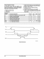
the feedback signals are pins 1 and 11. These configurations are summarized in Table 1 and illustrated in Figure 2.
.
Macrocell Configuration
SGO SG1 SLOx Cell Configuration Devices Emulated
Device Uses Registers
Registered Output Configuration
The control bit settings are SGO =0, SG1 =1 and SlOx =
O. There is only one registered configuration. All eight
product terms are available as inputs to the OR gate.
Data polarity is determined by Sl1 x. The flip-flop is
loaded on the lOW to HIGH transition of ClK. The feedback path is from Q on the register. The output buffer is
enabled by OE.
0
1
0
Registered Output
0
1
1
Combinatorial 1/0
1
0
0
Combinatorial
Output
1
0
1
Input
1
1
1
Combinatorial 1/0
Device Uses No Registers
Combinatorial Configurations
The PAlCE16V8 has three combinatorial output configurations: dedicated output in a non-registered device,
110 in a non-registered device and 110 in a registered device.
Dedicated Output In a Non-RegisteredDevice
The control bit settings are SGO =1, SG1 = 0 and SlOx =
O. All eight product terms are available to the OR gate.
Because the macrocell is a dedicated output, the feedback is not used. Because ClK andOE are not used in a
non-registered device, pins 1 and 11 are available as input Signals. Pin 1 will use the feedback path of MC7 and
pin 11 will use the feedback path of MCo.
PAL 16RB, 16R6,
16R4
PAl16R6,16R4
PAL 1OHB, 12H6,
14H4, 16H2, 10lB,
12l6, 14l4, 16L2
PAL12H6,14H4,
16H2, 12l6, 14L4,
1612
PAL16LB
Programmable Output Polarity
The polarity of each macrocell can be active HIGH or
active lOW, either to match output signal needs or to
reduce product terms. Programmable polarity allows
Boolean expressions to be written in their most compact
form (true or inverted), and the output can still be of the
desired polarity. It can also save "DeMorganizing"
efforts.
Selection is through a programmable bit Sl1 x which
controls an exclusive-OR Gate at the output of the ANDI
OR logic. The output is active-HIGH if SL1x is "1" and
active-lOW if Sl1 x is "0".
PALCE16V8H-15/25
vii
OE _ _ _ _ _ _ _ _ _ _---,
OE - - - - - - - - - - - - - ,
o
a
Registered Active HIGH
Registered Active LOW
Combinatorial 1/0 Active HIGH
Combinatorial 1/0 Active LOW
Combinatorial Output Active LOW
Combinatorial Output Active HIGH
~
~
a
Adjacent 110 pin
Dedicated Input
12015-005A
Figure 2. Macrocell Configurations
viii
PALCE16V8H-15/25
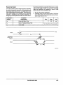
Power-Up Reset
This is equivalent to the standard logic notation below.
All flip-flops power up to a logic LOW for predictable system initialization. Outputs of the PALCE16V8 will depend onwhetherthey are selected as registered orcombinatorial. If registered is selected, the output will be
LOW. If combinatorial is selected, the output is a function of the logic.
~==D--AD
12015-007A
Figure 4. Standard AND Gate
Electronic Signature Word
An electronic signature word is provided in the
PALCE16V8 device. It consists of 64 bits of programmable memory that can contain user-defined data. The
signature data is always available to the user independent of the security bit.
Programming and Erasing
The PALCE16V8 can be programmed on standard logic
programmers. Approved programmers are listed in this
data sheet.
The PALCE16V8 may be erased to reset a previously
configured device back to its virgin state. Bulk erase is
automatically performed by the programming hardware.
No special erase operation is required.
Each vertical line in the PAL device is a potential input to
the AND gate. At each crosspoint is a programmable
bit, which provides a potential connection in the programmed state. The Xs in the diagram indicate a connection at the crosspoint.
In electrically erasable devices the crosspoints are originally disconnected. They are either connected or left
open during device programming.
Multiplexers in the PAL device logic diagrams use a simple notation for maximum clarity. A 2:1 multiplexer that
selects X when the control is LOW and Y when the
control is HIGH is shown below.
x
Security Bit
y
z
x
y
A security bit is provided on the PALCE16V8 as a deterrent to unauthorized copying of the array configuration
patterns. Once programmed, this bit defeats readback
of the programmed pattern by a device programmer, securing proprietary designs from competitors. However,
programming and verification are also defeated by the
security bit. The bit can only be erased in conjunction
with the array during a bulk erase cycle.
12015-00SA
Basic PAL Device Notation
Figure 5. PAL Device Multiplexer
The mUlti-input gates in the PAL device's programmable
AND gate array are simplified in the logic diagrams. The
PAL device notation for an AND gate, called a product
term in a PAL device, is shown below.
*I I *I I DABC
0
E
F
z
Notice that the control is operated by a programmable
cell that is initially disconnected from GND, floating to
Vcc, selecting the "1" path through the multiplexer.
When the cell is programmed, it is connected to GND
selecting the "0" path through the multiplexer.
A*D
12015-006A
Figure 3. PAL Device AND Gate
PALCE16V8H-15/25
ix
U<I1,
e>--{::::
r
~
0'
~
:
,
"'IT
rP~V
Yo.
ff
lP ~
o
....
,,~
0
0-
SGO
~
0'
00
~
:
'"
"
~
r
g:
0
SlO,
r-;;
~'O0'
Ii
.Vee
>rp ~
"
0'
00
o
II
0
-
••
e
~
r>--l:>
....
0
"
0-
~
SGI
.r:
~
&l
~
.."
-"""
rR
SG1J!t-SlO~
o.
Va:
,..,
~~
·
I,
SLO,
o
0
.
10
11
SGI
-0
:
~
'0
o.
00
~
·::
"
SlO,
....
~.oo.
n
.Yo.
SGI
SlO~
0: ~
>p ~~
r>----t
10
01
0."
...
12015-OO9A
x
-
0
PALCE16V8H-15/25
-Kl
Kl,
-
SGI
51.0,
rl=l
0
~ _ _ _~"1P~
:
~~~==~3-_-------------H---1~~==========~
SGI
51.0,
<J---<J0E/1
120154)9ot.
Concaodod
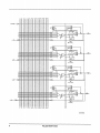
Figure 6. PALCE16V8 Logic Diagram
PALCE16V8H-15/25
xi
ABSOLUTE MAXIMUM RATINGS
OPERATING RANGES
Storage Temperature
Ambient Temperature under bias
Supply Voltage with Respect
to Ground
DC Output Voltage
Commercial (C) Devices
Temperature (TA) Operating
Free Air
Supply Voltage (Vee)
-65°C to +150°C
-55°C to +125°C
-O.SV to +7.0V
-O.SV to Vee +
O.SV
DC Input Voltage
-O.SV to Vee +
O.SV
Static Discharge Voltage
>2001 V
Latchup Current (TA= O°C to 75°C) >1 OOmA
O°C to +7SoC
+4.7SV to +S.2SV
Operating ranges define those limits between which the functionality of the device is guaranteed.
Stresses above those listed under ABSOLUTE MAXIMUM
RA TlNGS may cause permanent device failure. Functionality
at or above these limits is not implied. Exposure to absolute
maximum ratings for extended periods may affect device
reliability.
DC CHARACTERISTICS over operating range unless otherwise specified.
Parameter
Symbol
Parameter
Descriptions
Test Conditions
Min.
Max.
Unit
VOH
Output HIGH Voltage
Vee = MIN
VIN = VIH or VIL
10H = -3.2 rnA
VOL
Output LOW Voltage
Vee = MIN
VIN = VIH or VIL
10L = 24mA
VIH
Input HIGH Voltage
Voltage for all Inputs (Note 1)
Guaranteed Input Logical HIGH
VIL
Input LOW Voltage
Voltage for all Inputs (Note 1)
Guaranteed Input Logical LOW
0.8
V
I'H
IlL
Input Leakage Current
GND ~ V1N ~ Vee Max. (Note 2)
10
-10
~
10zH
10zL
Off-State Output Current
GND
10
-10
~
los
Output Short-Circuit Current
Vee = Max. VOUT = OV (Note 2)
-130
rnA
Icc
Supply Current
Outputs Open (10 = OA)
Vee = Max., F = 1SMHz
90
rnA
~
V1N
~
2.4
V
0.5
2.0
Vee Max. (Note 2)
-30
V
V
Notes:
1. These are absolute values with respect to device ground and all overshoots due to system or tester noise are included.
2. I/O pin leakage is the worst case of IlL and 10zL (or I'H and lozH)'
3. No more than one output should be shorted at a time and duration of the short-circuit should not exceed one second.
Capacitance (Note 1)
Parameter
Symbol
CIN
COUT
Parameter
Descriptions
Test Conditions
Typ.
Unit
Input Capacitance
Vee = S.OV, TA = +2SoC
5
pF
Output Capacitance
VIN = 2.0V at f = 1MHz
15
pF
Note:
1. These parameters are not 100% tested, but are evaluated at initial characterization and at any time the design is modi-
fied where capacitance may be affected.
xii
PALCE16V8H-15/25
SWITCHING CHARACTERISTICS over Commercial operating range (Note 1)
Parameter
Symbol
-15
Min.
Max.
Parameter
Description
-25
Min.
Max.
Unit
tpo
Input or Feedback to Combinatorial Output (Note 2)
ts
Setup Time from Input or Feedback to Clock
12
15
ns
tH
Hold Time
0
0
ns
tco
Clock to Output
10
12
ns
tCF
Clock to Feedback
8
10
ns
tWl
Width of Clock
tWH
f MAx
Maximum
Frequency
(Note 3)
15
25
LOW
8
10
HIGH
8
10
External Feedback 1/(ts+tco)
45.5
37
Internal Feedback 1/(tS+tCF)
50.0
40
No Feedback 1/(tWH+tWL)
62.5
40
ns
ns
MHz
t pzx
OE to Output Enable (Note 4)
15
20
t pxz
OE to Output Disable (Note 4)
15
20
ns
tEA
Input to Output Enable (Notes 4 and 5)
15
25
ns
tER
Input to Output Disable (Notes 4 and 5)
15
25
ns
ns
Notes:
1. Commercial Test Conditions: Rl = 200n, R2 = 390n (see switching test circuit).
2. t PD is tested with 8 1 closed and CL = 50pF (including jig capacitance). V1H = 3V, V1L = OV, VOH = VOL = 1.5V.
3. These parameters are not 100% tested, but are calculated at initial characterization and at any time the design is modified
where frequency may be affected.
4. For three-state outputs, enable times are tested with CL = 50pF to the 1.5V level; 8 1 is open for high-impedance to HIGH
tests and closed for high-impedance to LOW tests. Output disable times are tested with CL = 5pF. HIGH to highimpedance tests are made to an output voltage of VOH -O.5V with 8 1 open; LOW to high-impedance tests are made to an
output voltage of VOL to +0.5V with 8 1 closed.
5. Equivalent function to t pzx, t pxz but using product term control.
PALCE16V8H-15/25
xiii
SWITCHING WAVEFORMS
I
Input or
I
~
Feedback - - -.......
~
~~tPO
V
---
Logic
Combinatorial - - - Output
T
I
Register
~
tpD
12015-010A
I
Combinatorial Output
tCF
1201S-020A
CIOCk~
r-~CFltPD
Combinatorial--"":
Output____
VT
12015-019A
12015-013A
Input to Output Disable/Enable
Clock to Feedback to Combinatorial Output
(See Path at Right)
OE
Clock
Output
--_./
VOH" 0.5 V
VOL + 0.5 V
1201S-014A
12015-011A
Clock Width
Input or
OE to Output Disable/Enable
W
~
~_V_t
Feedback _ _ _ _ _
" _ : ......
+r=Vr_tH_+J
__
, ....._-_-_-_-_-_-_-
~
Clock
_________
Registered
Output
~~~tco
V·T---
~
12015-012A
Registered Output
Notes:
1. Vr = 1.5 V
2. Input pulse amplitude 0 V to 3.0 V
3. Input rise and fall times 2 - 5 ns typical
xiv
PALCE16V8H-15/25
SWITCHING TEST CIRCUIT
Vee
o--if 0 - - - - ,
Output o - - - - I I t - - - - - .
Switching Test Circuit
12015-019A
Notes on Testing Information
Specification
tPD• teo. tcF
tpzx• tEA
tpxz. tEA
Switch 51
CL
R1
R2
Closed
Measured Output Value
50 pF
200n
390n
1.5V
Z->H: Open
Z->L: Closed
50 pF
200n
390n
1.5V
H->Z: Open
L-> Z: Closed
50 pF
200n
390n
H->Z: VOH -0.5V
L->Z: VOL +0.5V
Key to Switching Waveforms
WAVEFORM
INPUTS
OUTPUTS
MUST BE
STEADY
WILL BE
STEADY
MAY CHANGE
FROM H TOL
WILL BE
CHANGING
FROMH TOL
0117
MAY CHANGE
FROM L TOH
WILL BE
CHANGING
FROML TOH
XXXXXX
DON'T CARE,
ANY CHANGE
PERMITTED
CHANGING,
STATE
UNKNOWN
\\\\\
12015A-018A
PALCE16V8H·15/25
xv
Output Register Preload
The PRELOAD function allows the registers to be
loaded from the output pins. This feature aids functional
testing of sequential designs by allowing direct setting of
output states. The procedure is as follows.
1. Raise Vee to 5.0 V ± 0.5 V.
2. Set pin 8 to 10.0 V ± 0.5 V.
3. Set DE HIGH.
Parameter
Symbol
tPlO
tps
tPH
tpcs
tPCH
dVrldt
dV,/dt
4. Apply the desired value (VIl..NIH) to all registered output pins. Leave combinatorial output pins floating.
5. Clock pin 1 from VIL to VIH.
6. Remove VIlJVIH from all registered outputs.
7. Lower pin 8 to VIlJVIH.
8. Enable the output registers by lowering OE.
9. Verify for VOLiVOH at all registered output pins. Note
that the output pin signal will be the inverse of the
preload input.
Parameter Description
Setup and Hold Time from Preload (pin 8) to DE
Setup Time from 'OE to Data
Hold Time from Data to OE
Setup Time from Data to Clock
Hold Time from Clock to Data
VPLD Rising Slew Rate (pin 8)
VPLD Falling Slew Rate (pin 8)
Min.
Rec.
50
1
1
1
1
10
50
1
1
1
1
2
Max.
Unit
100
3
J.lS
J.lS
J.lS
J.lS
J.lS
V/J.ls
V/J.ls
Pin8 - - - '
--V'H
-------V'L
DE - - - - - - -
~l>_-t-PH-_----_
tp_s}-
110 _ _ _ _ _ _ _
._~ tPC_}= t~ ~-tPC-H-:j-----------
Clock _ _ _ _ _ _ _ _ _ _ _ _
12015-<l15A
Preload Waveforms
xvi
PALCE16V8H-15/25
Power-Up Reset
The PALCE16V8 has been designed with the capability
to reset during system power-up. Following power-up,
all flip-flops will be reset to LOW. The output state will be
HIGH independent of the logic polarity. This featu re provides extra flexibility to the designer and is especially
valuable in simplifying state machine initialization. A
timing diagram and parameter table are shown below.
Parameter
Symbol
1. The Vee rise must be monotonic.
2. Following reset, the clock input must not be driven
from LOWto HIGH until all applicable input and feedback setup times are met.
Parameter
Descriptions
Min.
tPR
Power-Up Reset Time
ts
Input or Feedback Setup Time
tw
Clock width
Power
Due to the synchronous operation of the power-up reset
and the wide range of ways Vee can rise to its steady
state, two conditions are required to insure a valid
power-up reset. These conditions are:
_ _ _ _oJ
Unit
100
Jls
See Switching Characteristics
------------------------------------------------ Vee
~
4V
Max.
...
~----------
tpR - - - - -....
Registered
Active LOW
Output _ _ _ _ _ _ _ _ _ _ _ _ _ _ _ _ _ _-L..
Clock
12015-{)17A
PALCE16V8H-15/25
xvii
fMAX
Parameters
The parameter fMAx is the maximum clock rate at ~~i?h
the device is guaranteed to operate. Because flexibility
inherent in programmable logic devices offers a choice
of clocked flip-flop designs, fMAx is specified for three
types of synchronous designs.
The first type of design is a state machine with feedback
signals sent off-chip. This external feedback C?ul~ go
back to the device inputs, or to a second device In a
multi-chip state machine. The slowest path defining the
period is the sum of the clock-to-output time and the
input setup time for the external signals (ts:+ tco). The
reciprocal, fMAX, is the maximum frequencywlth external
feedback or in conjunction with an equivalent speed
device. This fMAX is designated '1MAX external."
The second type of design is a single-chip state machine with internal feedback only. In this case, flip-flop
outputs are defined by the. device inpu.ts ~n~ f~ip-flop
outputs. Under these conditions, the penod IS limited by
the internal delay from the flip-flop outputs through the
internal feedback and logic to the flip-flop inputs (ts +
tCF). This fMAX is designated '1MAX internal".
The third type of design is a simple data path application. In this case, input data is presented to the flip-flop
and clocked through; no feedback is employed. Under
these conditions, the period is limited by the sum of the
data setup time and the data hold time (ts + tH). However,
as lower limit for the period of each fMAX type is the minimum clock period (tWH + tWL). Usually, this minimum
clock period designates the period forthe third fMAx, designated "fMAX no feedback".
ClK
r-------------------,I
I
1 ~
I --
Ir~
!
lOGIC
---...
~
....~I....-
REGISTER
~ECOND
CHIP)
I
I
il I
_ _ JI
I~ _ _ _ _ _ _ _ _ _ _ _ _ _ _ _ _ _ ~
fmax External Feedback; 1/(ts + teo)
ClK
ClK
r-------------------,I
r------------- -----,I
I
I
I
I
lOGIC
I
REGISTER
I
I
I
_
_
_
_
_
_
_
_
_
_
_
_
_
_
_
_
_
_
_
J
I
I
~
1
....
1---- t S
..
----t·~I~I - - - t CF
I
I
I ~
I
I
lOGIC
--:.....
REGISTER
1--",
~
I
I _ _ _ _ _ _ _ _ _ _ _ _ _ _ _ _ _ _ _ JI
1
I
-
~
--..J
fmax Internal Feedback; 1/(ts + b)
fma• No Feedback; 1/(ts + tH) or 1/(tWH + twd
12015-020A
xviii
PALCE16V8H-15/25
PHYSICAL DIMENSIONS
PD020
1
. . .......-- 1.010
1.040 - - - - - - - I..~I
T
.240
.290
~6~~~~~~~~~~~ ~
~l.045
.065
.090
.110
~~
.005
MIN .
.005
.14Qt,~ .OfO
.20~
~
+
.125
.160
T~~
.014
.023
12015-021A
PL020
.042
.048
.020
MIN
.050
REF
--. r-
.025
1/.045
R
r
.385
.395
.350
.356
.026
-.032
.009
.015
069700
PALCE16V8H-15/25
xix
Programmers/Development Systems (Subject to change)
MANUFACTURER
PROGRAMMER CONFIGURATION
Adams MacDonald
2999 Monterey/Salinas Hwy.
Monterey, CA 93940
(408) 373-3607
Contact Manufacturer
Data I/O Corporation
Willow Road NE
PO Box 97046
Redmond, WA 98073-9746
(800) 247-5700
System 29B
LogicPakTII 303A-V04
Adapter 303A-DllA1Rev. Vl0
UniSite
Rev. 2.5
Family/Pinout Code
80-55
Digelec Inc.
1602 Lawrence Avenue, Suite 113
Ocean, NJ 07712
(201) 493-2420
Contact Manufacturer
Kontron Electronics Inc.Contact Manufacturer
1230 Charleston Road
Mountain View, CA 94039-7230
(415) 965-7020
Contact Manufacturer
Logical Devices
1201 E. Northwest 65th Place
Fort Lauderdale, FL 33309
Contact Manufacturer
Micropross
Pare d'Activite des Pres
5, rue Denis-Papin
59650 Villeneuve-d'Ascq
(20) 47.90.40
Contact Manufacturer
Stag Microsystems Inc.
1600 Wyatt Drive, Suite 3
Santa Clara, CA 95054
(408) 988-1118
Contact Manufacturer
Varix Corporation
1210 E. Campbell Road, Suite 100
Richardson, TX 75081
(214) 437-D777
Contact Manufacturer
MANUFACTURER
SOFTWARE DEVELOPMENT SYSTEM
Advanced Micro Devices
901 Thompson Place
Sunnyvale, CA 94088-3453
(800) 222-9323
PALASM 2.23D
Data I/O Corporation
10525 Willow Road NE
PO Box 97046
Redmond, WA 98073-9746
(800) 247-5700
Contact Manufacturer
Personal CAD Systems
Assisted Technology Division
1290 Parkmoor Avenue
San Jose, CA 95126
(408) 971-1300
Contact Manufacturer
PAL, PALASM, and SKINNYDIP are registered trademarks of Advanced Micro Devices.
LogicPak and UniSite are trademarks of Data I/O Corporation.
GAL is a registered trademark of Lattice Semiconductor Corp.
This part is covered by various U.S. and foreign patents owned by Advanced Micro Devices.
xx
PALCE16V8H-15/25
PALASM 2 SOFTWARE
SUPPORT FOR THE
PALCE16V8
About this Section
This section describes PALASM 2 software special considerations for the
PALCE16V8. It is intended as a supplement to the PALASM 2 software user
documentation in part 4 of the 1988 PAL Device Data Book. -If you do-not
already have the-Data Book, -contact-your-Iocal AMD sales-office for a copy.
Boolean Equation Design Entry
1.
The pin list for the PALCE16V8 follows.
;1
eLK
;11
OE
2
12
3
13
4
14
5
IS
6
16
7
I7
8
18
9
19
GND
10
12
01
13
02
14
03
15
04
16
05
17
06
18
07
19
08
vee
20
Note: The lines beginning with a semicolon (;) are comments and are
ignored by the software.
2.
You use the SIGNATURE command to program the signature fuse. The
command must be used in the Declaration segment of your design file.
It must follow the CHIP statement. If you enter it in the Equations
segment, the software displays an error message.
The signature command syntax follows.
Advanced Micro Devices
a-1
PALASM 2 Software Support for the PALCE16V8
Syntax
SIGNATURE
number
or
string
Each of the syntax options is defined below.
Syntax option 1:
SIGNATURE
=
number
The number you use can be
binary
#8 or#b
octal
#Oor#o
decimal
#D or#d
hexadecimal
#H or#h
Notice that each number base is specified by an upper case·or·lower
case designator. The examples below illustrate different ways to
specify the signature as a number.
Examples
SIGNATURE
123456
SIGNATURE
#D845
SIGNATURE
#H
1976A5
Note the following
The space in .the last example .is .allowed, but is deleted by the
software.
Number designators are optional. If you do not use a number
designator, the software assumes a decimal number.
a-2
Advanced Micro Devices
PALASM 2 Software Support for the PALCE16V8
The 64 least significant bits are programmed. The remaining most
significant bits on the left are truncated.
The software does not program decimal numbers greater than 15
digits.
Syntax option 2:
SIGNATURE
=
string
Examples
SIGNATURE
abcdefgh
SIGNATURE
ABC 123
Note the following.
A string must begin with an alpha character.
Alphanumeric characters and underscores are allowed.
The software converts alpha characters to the corresponding
ASCII code.
Spaces are allowed in strings.
The software converts all lower case characters that you enter into
upper case .characters.
The left-most 8 characters are programmed with the corresponding
ASCILcode. The remaining characters.ontheright ar.etruncated.
Simulation
The PRELOAD command replaces the old PRLDF command described in
Chapter 4 of the PAL Data Book.
Include the PRELOAD command in the simulation segment of your PDS
design file. The syntax for the PRELOAD command follows.
Advanced Micro Devices
a-3
PALASM 2 Software Support for the PALCE16V8
Syntax
list of register identifiers
PRELOAD
Example
PRELOAD 01 /02 03
The example above shows the PRELOAD command setting the register
values to 101 (high, low, high).
The PRELOAD command is similar to the old PRLDF command. It forces a
register into a known state, either 1 or O. The PRELOAD statement allows
you to initialize registers.
Figure 1 illustrates a PALCE16V8 output register. Notice the register is
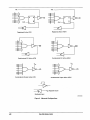
identified by the output node name A.
Figure 1: Output Register
To set the A register value to 1, the PRELOAD statement is written as shown
in the example below.
Example
PRELOAD A
In the example above, the PRELOAD command sets the register to a value
of 1. The inverter causes the output value to change to O. Thus, the
PRELOAD command determines the value of the register alone. The -output
value is determined by the device architecture.
a-4
Advanced Micro Devices
PALASM 2 Software Support for the PALCE16V8
Note: Unlike the PRELOAD command, the old PRLDF command determined
the value of outputs not registers.
The example below shows a partial simulation segment for a PALCE16V8.
Example
CHECK 014 /015 016 /017
SETF OE
PRELOAD /014 /015 016 017
;Preload registers=0010
SETF JOE
CHECK 014 015 /016 017
iCheck output
CLOCK CLK
CHECK 014 /015 016 /017
iNext state
Note: The above example assumes the pin list shown earlier in this
document.
Keep the following special considerations in mind when using the PRELOAD
command on the PALCE16V8.
The register is forced to a known state and the output is calculated from
the register.
After the register is clocked, the value that represents the next state
appears at the output.
An error is generated if the output is not disabled before preload.
The PRELOAD statement works on the register; the CHECK statement
validates the output.
Advanced MIcro DevIces
a-5
DESIGN A DECODER FOR
THE PALCE16V8
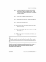
About this Tutorial ............................................................................................. ·.·.·.·.·.·.·N· .••2
Install the Software ................................... ~ ............................. 3
Learn the Menu ...................................................................... 4
Create the Decoder Design ......................................................... 6
Learn the Structure of the PALASM Design File ...................... 8
Build the Declaration Segment ........................................... 8
Build the Simulation Segment .......................................... 15
Process the Design File .......................................................... 22
Autorun Compile and Simulate ......................................... 23
View the Output Files ............................................................ 26
View the Compile Output Files ......................................... 27
View the Simulation Output Files ...................................... 28
About this Tutorial
About this Tutorial
This tutorial is a step-by-step procedure on using P ALASM software to
design a decoder for the PALCE16V8. It describes only those features of
PALASM software that are-required"forthe decoder design. Therefore,-it
works merely as an introduction to P ALASM software. The full featured
version of the software provides you with additional design capability for
advanced applications. Contact your local Advanced Micro Devices _sales
office for a full-featured version ofPALASM software. The software
package includes a comprehensive user manual.
Prerequisites
You need an IBM-PC/XT/ATorcompatiblewith
a hard disk.
You need the two software disks labelled
PALCE16V8 Evaluation Kit.
To program the PALCE16V8 sample, a
programmer must be linked up to your computer.
To communicate with the programmer, a
programmer communications program of your
choice must be installed on your computer.
How to Use this Tutorial
This tutorial is designed to be read sequentially from beginning to end.
First you install the software, then create a Boolean equation design,
compile the design, simulate the design, and finally view the output files.
The process takes approximately one hour.
2 Design a Decoder for the PALCE16V8
March 1989
Install the Software
Install the Software
The software on the two floppy disks labelled PALCE16V8 Evaluation Kit
has been compressed into archive format. The installation procedure
dearchives the software programs before installing them on your hard disk.
This procedure takes approximately seven minutes.
Step 1. Place disk #1 in drive A.
Enter
Step 2.
A: INSTALL <return>
At the prompt, specify .the drive on which you want
the software installed.
Step 3. At the prompt, if necessary, allow the software to
make changes to the system files AUTOEXEC.BAT
and CONFIG.SYS.
Step 4. When the message window at the bottom of your
screen prompts you, place disk #2 in drive A.
Step 5. When the installation procedure is complete, the
following message appears on your screen.
Re-boot and enter C: PALC16V8
Follow the instructions to start up the program.
Note
The command to call up the software is PALC16V8 and not PALCE16V8.
March 1989
Design a Decoder for the PALCE16V8 3
Learn the Menu
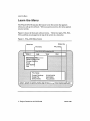
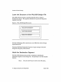
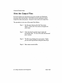
Learn the Menu
The PALCE16V8 Evaluation Kit banner is the fIrst screen that appears
when you call up the software. When you press any key, the menu appears
on your screen.
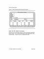
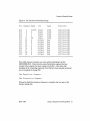
Figure 1 shows the four part software menu. These four parts, File, Edit,
View and Run are arranged at the top of the screen in a menu bar.
Figure 1. PALASM Menu Screen
Status line
Menu bar
4 Design
a Decoder for the
PALCE16V8
March 1989
Learn the Menu
Each of the menu bar items contains a different set of program options
related to that menu function. For example, the optionsfor-findrnga file or
a directory are located in the File menu. When you highlight one menu bar
item, its menu appears. Notice that you can move laterally across the screen
using the cursor movement arrows.
The status line at the bottom of the screen gives information about how to
control the screen. Check this information frequently because the
information changes as you perform "different tasks. Use the "arrow "keys to
move the cursor to the operation you wish to perform.
Get familiar with the menu by exploring the various options. When you are
ready to begin using the software functions, proceed to Create the Decoder
Design.
March 1989
Design a Decoder for the PAlCEfSV8 5
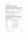
Create the Decoder Design
Create the Decoder Design
The simple decoder design is created in Boolean equations and implemented
in a PALCE16V8 device. Your first task in creating the design is to
understand the function of the decoder and interpret the function in Boolean
equations.
Note
Although decoders are usually combinatorial,Jor the purpose oJthis
exercise assume a registered decoder design.
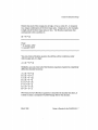
The Function of the Decoder
Table 1 shows a truth table for the decoder. The decoder has three input
pins: X, Y, and Z. The function of the decoder is to monitor the three input
pins and assert one of eight output lines, A-H, for each of the eight
combinations of inputs.
Table 1. Truth Table for Decoder
Inputs
Outputs Generated
X Y Z
A B C D E F G H
0 0 0
0 0 1
0 1 0
0 1 1
1 0 0
1 0 1
1 1 0
1
1
1
1
0
0
0
0
0
0
0
6 Design a Decoder for the PALCE16V8
0 0
1 0
0 1
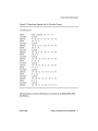
0 0
0 0
0 0
0 0
0 0
0 0 0 0
0 0 0 0
0 0 0 0
1 0 0 0
0 1 0 0
0 0 1 0
0 0 0 1
0 0 0 0
0
0
0
0
0
0
0
1
March 1989
Create the Decoder Design
Notice that each of the output pins is high, or has a value of 1, in response
to a unique combination of the three input pins. Output pin A, for example,
is high only if the three input pins are low. The Boolean expression that
corresponds to this condition is
!X*/y*!Z
Note
* is used/or AND
/ is used/or NOT
You can create a Boolean equation that defines all the conditions under
which output pin A is high:
A=!X*/Y*!Z
Similarly, you can create all of the Boolean equations required to completely
define the decoder functions:
A=!X*/Y*!Z
B=!X*/Y*Z
C=!X*Y*/Z
D=!X*Y*Z
E=X*/Y*/Z
F=X*/Y*Z
G=X*Y*/Z
H=X*Y*Z
Now that you have Boolean equations to describe the decoder functions, it
is time to create a complete PALASM -design file for the decoder.
March 1989
Design a Decoder for the PALCE16V8 7
Create the Decoder Design
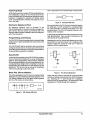
Learn the Structure of the PALASM Design File
PALASM software requires a specific design file layout. Figure 2
illustrates the layout. The equations defined above go into the Equations
segment of the file.
Figure 2. PALASM Design File Layout
I
[:~OOA~ONS SEGM~~
I
:I
DIECLAlRAlI"~OINl SIEGLVllElNlll"
::
SIMUlAl100 SEGMENT
..:
:' :']
'I
The PALASM design file is also known as the PDS (PAL device Design
Specification) file.
Proceed to Build the Declaration Segment to begin creating the decoder
design file using PALASM software.
Build the Declaration Segment
The PALASM software menu provides a template for building the
Declaration segment of your design file. The procedure to use the template
follows.
Step 1. Use your arrow keys to move to the File menu ..
8 Design a Decoder for the PALCE16V8
March 1989
Create the Decoder Design
Step 2.
Select New Design File in the File menu and press
<return>.
Step 3. A window appears. Enter a file name of your
choice. This tutorial uses the file name shown
below.
Enter
DECODER.PDS <return>
The PDS Declaration Segment-template appears·on
your screen.
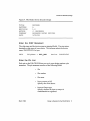
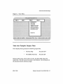
Figure 3 shows the template as it appears on your screen. Notice you can
use <return> to move from field to field. However, some fields require you
to enter information before you can move on. Also, use FlO and not
<return> to save the segment.
March 1989
Design a Decoder for the PALCE16V8 9
Create the Decoder Design
Figure 3. Screen Template of PDS Declaration Segment
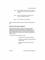
Enter the File Header Information
The first part of the Declaration segment consists of descriptive information
about your file. You can enter the following or similar information for the
decoder design. Figure 4 shows the completed file header.
10 Design a Decoder for the PALCE16V8
March 1989
Create the Decoder Design
Figure 4. File Header for the Decoder Design
TITLE
PATTERN
REVISION
AUTHOR
COMPANY
DATE
DECODER
A
1.0
J. ENGINEER
ADVANCED MICRO DEVICES
3/20/89
Enter the CHIP Statement
The chip name and the device name are required fields. You can enter a
descriptive chip name of your choice. The software selects the device
name, PALCE16V8, for you.
CHIP
ChipName
=
PAL AMD
Device
PALCE16V8
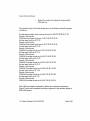
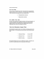
Enter the Pin List
Each pin on the P ALCE 16V8 that you use in your design requires a pin
statement. The pin statement consists of the following fields.
Pin
Pin number
Pin name
Input, output, or I/O
Specify one of the above.
Input or Output type
Specify whether the input or output is
combinatorial or registered.
March 1989
Design a Decoder for the PALCE16V8 11
Create the Decoder Design
Polarity type
Specify whether the output is active-low or
active-high.
In Create the Decoder Design notice that the decoder design consists of three
inputs and eight outputs. In addition, you must define pin 1 as the·c1ockpin
and pin 11 as the output enable pin.
The procedure to enter the pin list follows.
Step 1. Enter the pin statements using the arrow keys or the
tab key to move from field to field. Notice that the
template allows you to save time by giving you
choices for several of the fields
Figure 5 shows the completed· pin list.
Step 2.
Press FlO, not <return>, to save your pin list·and
exit the template
12 Design a Decoder for the PALCE16V8
March 1989
Create the Decoder Design
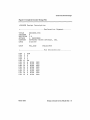
Figure 5. Pin List for the Decoder Design
Pin Number Name
I/O
Type
Polarity
Pin
Pin
Pin
Pin
Pin
Pin
Pin
Pin
Pin
Pin
Pin
Pin
Pin
Input
Input
Input
Input
Input
Output
Output
Output
Output
Output
Output
Output
Output
Comb
Comb
Comb
Comb
Comb
Reg
Reg
Reg
Reg
Reg
Reg
Reg
Reg
Active-high
Active-high
Act"ive-high
Active-high
Active-high
Active-high
Active-high
Active-high
Active-high
Active-high
Active-high
Active-high
Active-high
1
2
3
4
11
12
13
14
15
16
17
18
19
CLOCK
X
y
Z
OE
A
B
C
D
E
F
G
H
PALASM software transfers you to the editor and displays the file
DECODER.PDS. Notice that the entire Declaration segment that you
created in the template has been copied into the file. Also notice that
headings of the remaining segments of the file have been entered to prompt
you to complete the design file:
The Equations Segment
The Simulation Segment
Proceed to Build the Equations Segment to complete the next part of the
decoder design file.
March 1989
Design a Decoderforthe PALCE16V8 13
Create the Decoder Design
Build the Equations Segment
The Equations segment contains the Boolean equations that specify the
decoder design.
In Table 1, the truth table defines the desired outputs A-H as a function of
the inputs X, Y, and Z.
Figure 6 shows the complete equations segment for the decoder design file
Figure 6. Equations Segment for the Decoder Design
EQUATIONS
A
B
c
D
E
F
G
H
Ix
Ix
Ix
Ix
X
X
X
X
* Iy * Iz
* Iy * z
* y * Iz
* y * Z
* Iy *
* Iy *
* Y *
* Y *
Iz
Z
Iz
Z
After exiting the PDS Declaration Segment template, the software displays
the file DECODER.PDS on your screen. You are now in the editor. Until
you quit the editor and return to P ALASM, use the editor commands. The
procedure to enter the Boolean equations in the Equations segment of the
DECODER.PDS file follows.
Step 1.
Use the arrow key to move the cursor to the line just
under the keyword EQUATIONS.
14 Design a Decoder for the PALCE16V8
March 1989
Create the Decoder Design
Step 2.
Enter the Boolean equations as shown in Figure 6.
At the end of each line, press <return> to go to the
next line.
Step 3. When you have entered all the equations, press
<escape> to display the menu bar.
Step 4.
Go to the File menu, and select Save.
Proceed to Build the Simulation Segment to complete the decoder design
file.
Build the Simulation Segment
This segment of the design file is optional. Including the simulation
segment in the design file makes simulation of the design possible.
Simulation allows you to predict the behavior of your design in software.
The PALASM simulator allows you to monitor the status of inputs and
outputs, to control the input signals, and to check the outputs against your
predicted outputs.
To simulate this design thoroughly, you must
Set the inputs in every possible combination.
Check if each combination of inputs produces the
desired outputs.
Supply a clock pulse to effect the change in
outputs.
March 1989
Design a Decoder for the PALCE16V8 15
Create the Decoder Design
Enable the outputs by setting the output enable
CaE) pin low.
The simulation for the decoder design may be described in natura1language
as follows.
Set the output enable, clock, and input levels to JOE /CLOCK IX IY /Z.
Supply a clock pulse.
Check that the output levels are AlB /C ID IE IF /G /H.
Set the input levels to IX IY Z.
Supplya-c1ock·pulse.
Check that the output levels are /A B /C ID IE IF /G /H.
Set the input levels to IX Y /Z.
Supply a clock pulse.
Check if the output levels are / A IB C ID IE IF /G /H.
Set the input levels to IX Y Z.
Supply a clock pulse.
Check if the output levels are / AlB /C D IE IF /G /H.
Set the input levels to X IY /Z.
Supply a clock pulse.
Check if the output levels are / A IB /C ID E IF /G /H.
Set the input levels to X IY Z.
Supply a clock pulse.
Check if the output levels are / AlB /C ID IE F /G /H.
Set the input levels to X Y /Z.
Supply a clock pulse.
Check if the output levels are / A IB /C ID IE IF G/H.
Set the input levels to X Y Z.
Supply a clock pulse.
Check if the output levels are / A IB /C ID IE IF /G H.
PALASM uses simple commands to define the simulation instructions.
Figure 7 shows the completed simulation segment for the decoder design in
PALASM syntax.
16 Design a Decoder for the PALCE16V8
March 1989
Create the Decoder Design
Figure 7. Simulation Segment for the Decoder Design.
SIMULATION
SETF
CLOCKF
CHECK
SETF
CLOCKF
CHECK
SETF
CLOCKF
CHECK
SETF
CLOCKF
CHECK
SETF
CLOCKF
CHECK
SETF
CLOCKF
CHECK
SETF
CLOCKF
CHECK
SETF
CLOCKF
CHECK
IOE ICLOCK Ix Iy IZ
CLOCK
A IB IC
Ix Iy Z
CLOCK
IA B IC
Ix
y
ID IE IF IG IH
ID IE IF IG IH
Iz
CLOCK
IA IB C ID IE IF IG IH
Ix y Z
CLOCK
IA IB IC
D
X Iy Iz
CLOCK
IA IB Ic ID
IE IF IG IH
E
X Iy Z
CLOCK
IA IB IC ID IE
IF IG IH
F
X Y Iz
CLOCK
IA IB IC ID IE IF
IG IH
G
IH
X y Z
CLOCK
IA IB IC ID IE IF IG
H
The procedure to enter the Simulation commands in the DECODER.PDS
file follows.
March 1989
Design a Decoder for the PALCE16V8 17
Create the Decoder Design
Step 1. In the editor file, DECODER.PDS, use the arrow
key to move the cursor just under the keyword
SIMULATION.
Step 2.
Enter the Simulation segment shown in Figure 7. At
the end of each line, press <return> to go to the next
line.
Step 3. When you have entered all the equations, press
<escape> to display the menu bar.
Step 4.
Go to the File menu, and select Save.
Step 5.
Figure 8 shows you the comp1ete-decoder-design
file. Check your editor me to see if there are any
typos. Your file will not process -correctly if there
are syntax errors. Correct your errors and save the
file again.
Step 6.
Press <esc> to call up the editor menu bar.
Step 6.
Select Quit All Files in the Quit menu to return to
PALASM.
The decoder design file is now complete and ready for PALASM to
process. Proceed to Process the Design File_.
18 Design a Decoder for the PALCE16V8
March 1989
Create the Decoder Design
Figure 8 Complete Decoder Design File
;PALASM Design Description
; . . . . . . . . . . . . . . . . . . . . . . . Declaration Segment ...... .
TITLE
PATTERN
REVISION
AUTHOR
COMPANY
DATE
DECODER.PDS
A
1.0
J. ENGINEER
ADVANCED MICRO DEVICES, INC.
3/20/89
PAL AMD
CHIP
PALCE16v8
; . . . . . . . . . . . . . . . . . . . . . . . Pin Declarations
PIN
PIN
PIN
PIN
PIN
PIN
PIN
PIN
PIN
PIN
PIN
PIN
PIN
1
2
3
4
11
12
13
14
15
16
17
18
19
March 1989
..........
CLK
X
Y
Z
OE
A HIGH
B
HIGH
C HIGH
D HIGH
E HIGH
F
HIGH
G HIGH
H HIGH
REG
REG
REG
REG
REG
REG
REG
REG
Design a Decoder for the PALCE16V8 19
Create the Decoder Design
; . . . . . . . . . . . . . . . . . . . . . . . Boolean Equations Segment.
EQUATIONS
A
B
c
D
E
F
G
H
Ix
Ix
Ix
Ix
X
X
X
X
*
*
*
*
*
*
*
*
Ix * Iz
Iy * z
y * Iz
y
*
Z
Iy * Iz
Iy * Z
Y * Iz
Y *
Z
20 Design a Decoder for the PALCE16V8
March 1989
Create the Decoder Design
; . . . . . . . . . . . . . . . . . . . . . . . Simulation Segment ............. .
SIMULATION
SETF
CLOCKF
CHECK
SETF
CLOCKF
CHECK
SETF
CLOCKF
CHECK
SETF
CLOCKF
CHECK
SETF
CLOCKF
CHECK
SETF
CLOCKF
CHECK
SETF
CLOCKF
CHECK
SETF
CLOCKF
CHECK
March 1989
JOE /CLOCK /X /Y /z
CLOCK
A /B /C /D /E /F /G /H
/X /Y Z
CLOCK
/A B /C /D /E /F /G /H
/X Y /z
CLOCK
/A /B C /D /E /F /G /H
/X Y Z
CLOCK
/A /B /C D /E /F /G /H
X /Y /z
CLOCK
/A /B /C /D E /F /G /H
X /Y Z
CLOCK
/A /B /C /D /E F /G /H
X Y /z
CLOCK
/A /B /C /D /E IF G /H
X Y Z
CLOCK
/A /B /C /D /E /F /G H
Design a Decoder for the PALCE16V8 21
Create the Decoder Design
Process the Design File
Before you begin processing the decoder design created.in the previous
sections, take a look at the software processing sequence.
The processing sequence consists of two simple steps.
1. Compile the design .and .generate JEDEC .output.
2. Simulate the design.
The main purpose of using PALASM is to translate your input·design ·into
programmer-readable JEDEC output. However, through ·simulation,
PALASM allows you to test your design without actually programming a
device.
Figure 8 illustrates the software processing sequence. Notice that both the
compile and Simulation processes generate output files.
Figure 9. PALASM Software Processing Sequence
Compile
the Design
I
[
Simulate
the Design
Fuse Map
JEDEC Fuse Data
__ Simulation History
~
_
22 Design a Decoder for the PALCE16V8
Simulation Trace
JEDEC Test Data
March 1989
Create the Decoder Design
Now that you have an overview of the procedure, you can begin processing
the decoder design. Proceed to Autorun Compile and Simulate.
Autorun Compile and Simulate
Use the arrow keys to go to the Run menu in PALASM. Notice that the
Run menu offers you three choices. Figure 9 illustrates the Run menu.
Figure 10. Run Menu
PALASM software offers you a time saving autorun feature that combines
the compile and Simulation processes into one keystroke. The autorun
procedure follows.
Step 1.
March 1989
Select Autorun in the Run menu
A window opens at the bottom of your screen.
Design a Decoder for the PALCE16V8 23
Create the Decoder Design
Step 2. Watch the status line as PALASM software
completes the following operations.
Parse
Minimize
Assemble
Simulate
Step 3. When you see the message
PLDSIM Program Successful
Press <esc>.
If the process was successful, you can skip steps 411.
If the process was unsuccessful-and produces errors,
proceed to step 4.
Step 4.
Select Edit in the PALASM menu bar. The Edit
menu appears on your screen.
Step 5. Select Design File in the Edit menu. The design file
DECODER.PDS appears.
24 Design a Decoder for the PALCE16V8
March 1989
Create the Decoder Design
Step 6.
Carefully compare the file on your screen with the
printed file in Figure 8, Complete Decoder Design
File. If your have typos in your screen file, make the
necessary changes.
Step 7. Press <esc> to display the editor menu bar.
Step 8. Select File in the menu bar. The File menu appears.
Step 9.
Select Save in the File menu.
Step 10. To quit the editor, select Quit in the menu bar. The
Quit menu appears.
Step 11. Select Quit All Files. The software returns you to the
PALASM menu.
Step 12. Now repeat steps 1-3 to recompile and simulate your
design file.
Note
The decoder design has been tested andfound error1ree. If your compile
and simulation processes produce errors, you probably have typos in your
file.
Now that the design file has been successfully processed, you can look at
the output files that the compile and simulation processes generated.
Proceed to View the Output Files.
March 1989
Design a Decoderforthe PALCE16V8 25
Create the Decoder Design
View the Output Files
In the last section you used autorun to run the compile and Simulation
processes with one keystroke. PALASM, however, generates a set of
output files after each process. Proceed to view each set of output files.
The procedure to view any of the output files follows.
Step 1. Use the arrow keys to select the View menu.
Figure 11 shows the View menu as it appears on
your screen
Step 2.
Notice that the list contains input, .output.and
intermediate files. To view a file, select the item and
press <return>
Step 3. The file is now displayed on your screen. Notice
you can scroll up and down using the arrow keys.
Step 4. Press <esc> to exit the file.
26 Design a Decoder for the PALCE16V8
March 1989
Create the Decoder Design
Figure 11. View Menu
:Bu.6tifu~JQg:::{:
Input data
Fuse map
JEDEC fuse data
JEDEC test data
Simulation history
Simulation trace
View the Compile Output Files
The compile process generates the following output files.
The Fuse Map
Decoder XPT
The JEDEC Fuse Data
Decoder.lED
Notice the file names, shown.above in italic, that PALASM assigns the
output files. The first part of the name is user-defined. The second part is
the extension that the software assigns.
March 1989
Design a Decoder for the PALCE16V8 27
Create the Decoder Design
The Fuse Map
The fuse map is a detailed map of the connections that are programmed
along each product term on the device. The following symbols illustrate
which connections are programmed and unprogrammed.
x
Unprogrammed connection
-
Programmed connection
The JEDEC Fuse Data
This file is the programmer-readable translation of the input design file. It
can be downloaded to the programmer to program the PALCE16V8.
JEDEC stands for Joint Electronic Device Engineering Council, the
organization that creates the standards for this file.
View the Simulation Output Files
The Simu1ation output ·files show you whether your design produces the
desired outputs. The Simulation process produces the following output
files.
Simulation History
Decoder.HST
Simulation Trace
Decoder.TRF
JEDEC Test Data
DecoderJDC
The decoder design does not use the TRACE command. Therefore, the
trace file is not generated and is not discussed in this tutorial.
28 Design a Decoderforthe PALCE16V8
March 1989
Create the Decoder Design
The Simulation History
The simulation history shows the status ·ofall the signals defined in the pin
list. It uses symbols to represent the different states:
H
High
L
Low
x Undefined
z
Output disabled
Figure 12 shows a sample history file.
Figure 12. Sample Simulation History File
"g" represents
SETF
I
I
"e" represents
CLOCKF
g cg cg cg cg cg cg cg c
CLOCK LHLLHLLHLLHLLHLLHLLHLLHL
LLLLLLLLLLLLLHHHHHHHHHHH
x
y
LLLLLLHHHHHHLLLLLLHHHHHH
LLLHHHLLLHHHLLLHHHLLLHHH
Z
LLLLLLLLLLLLLLLLLLLLLLLL
OE
HHHLLLLLLLLLLLLLLLLLLLLL
A
LLLHHHLLLLLLLLLLLLLLLLLL
B
LLLLLLHHHLLLLLLLLLLLLLLL
C
D
LLLLLLLLLHHHLLLLLLLLLLLL
E
LLLLLLLLLLLLHHHLLLLLLLLL
LLLLLLLLLLLLLLLHHHLLLLLL
F
LLLLLLLLLLLLLLLLLLHHHLLL
G
H
LLLLLLLLLLLLLLLLLLLLLHHH
March 1989
Design a Decoder for the PALCE 16V8 29
Create the Decoder Design
The JEDEC Test Data
The simulation process generates test vectors that are added to the JEDEC
file discussed in The JEDEC File above. The test vectors can be used to test
and verify the design on the device programmer.
This completes the PALASM design and simulation process. The next step
is to download your JEDEC file to a device programmer. Consult the
Programmers Development Systems Table in this data sheet part of this
document for information on programmers. Also, refer to your
programmer manual for instructions on setup and use.
Where to Go/rom Here
This tutorial did not explore all the capabilities of P ALASM software or the
PALCE 16V8. To order the full-featured version of P ALASM software,
contact your local AMD sales office today.
30 Design a Decoder for the PALCE16V8
March 1989
International (Continued) _ _ _ _ _ _ __
North American __________
ALABAMA .............................................................. (205) 882-9122
ARIZONA ............................................................... (602) 242-4400
CALIFORNIA,
Culver City ........................................................ (213) 645-1524
Newport Beach ................................................ !7141752-6262
Rosev[IIe ........................................................... 916 786-6700
San Diego ......................................................... 619 560-7030
San Jose .....: ..................................................... (408) 452-0500
Woodland Hills ................................................. (818) 992-4155
CANADA, Ontario,
K~nata ............................................................... (613) 592-0060
Willowdale ........................................................ (416) 224-5193
COLORADO .......................................................... (303) 741-2900
CONNECTICUT .................................................... (203) 264-7800
FLORIDA,
.
Clearwater ........................................................ (813) 530-9971
Ft. Lauderdale .................................................. (305) 776-2001
Orlando ............................................................. (407) 830-8100
GEORGIA .............................................................. (404) 449-7920
ILLINOIS,
Chicago ............................................................. (312) 773-4422
Naperville ......................................................... (312) 505-9517
KANSAS ................................................................. !913~ 451-3115
MARYLAND ........................................................... 301 796-9310
MASSACHUSETTS .............................................. 617 273-3970
MINNESOTA ...........................;................... :......... (612) 938-0001
MiSSOURI ............................................................. (913) 451-3115
NEW JERSEY,
CherrY Hill ......................................................... (609) 662-2900
Parsippany ....................................................... (201) 299-0002
NEW YORK,
Liverpool .....: ..................................................... (315) 457-5400
Poughkeepsie .................................................. (914) 471-8180
NORTH CAROLINA .............................................. (9 19) 878-8111
OHIO,
.
Columbus .......................................................... (614) 891-6455
Dayton ............................................................... (513) 439-0470
OREGON ............................................................... (503) 245-0080
PENNSYLVANIA .................................................. (215) 398-8006
SOUTH CAROLINA .............................................. (803) 772-6760
TEXAS,
Austin ................................................................ !5121346-7830
Dallas ................................................................ 214 934-9099
Houston ............................................................. 713 785-9001
International _______....:..-.___
BELGIUM, Bruxelles ....... TEL ............................. (02) 771-91-42
FAX ............................. (02) 762-37-12
TLX ............................................. 61028
FRANCE, Paris ................ TEL ............................ (l) 49-75-10-10
FAX ............................ (l) 49-75-10-13
TLX ........................................... 263282
WEST GERMANY,
Hannover area ............ TEL .............................. (0511) 736085
FAX .............................. (0511) 721254
TLX ........................................... 922850
MOnchen ...................... TEL ................................. (089) 4114-0
FAX ................................ (089) 406490
TLX ........................................... 523883
Stuttgart ....................... TEL ........................... (0711) 62 33 77
FAX .............................. (0711) 625187
TLX ........................................... 721882
HONG KONG ................... TEL ............................. 852-5-8654525
FAX ............................. 852-5-8654335
TLX .......................... 67955AMDAPHX
ITALY, Milan .................... TEL ................................ (02) 3390541
................................ (02) 3533241
FAX ................................ (02) 3498000
TLX ........................................... 315286
JAPAN,
Kanagawa .................... TEL ................................. 462-47-2911
FAX ................................. 462-47-1729
Tokyo ........................... TEL ............................... (03) 345-8241
FAX ............................... (03) 342-5196
TLX ........................ J24()64AMDTKOJ
Osaka ........................... TEL ................................. 06-243-3250
FAX ................................. 06-243-3253
KOREA, Seoul ................. TEL ............................... 822-784-0030
FAX ............................... 822-784-8014
LATIN AMERICA,
Ft. Lauderdale ............. TEL ............................. (305) 484-8600
FAX ............................ (305) 485-9736
TEL ................. 5109554261 AMDFTL
NORWAY, Hovik .............. TEL .................................. (02) 537810
FAX .................................. (02) 591959
TLX ............................................. 79079
SINGAPORE .................... TEL ................................... 65-3481188
FAX .................................. 65-3480161
TLX .......................... 55650 AMDMMI
SWEDEN,
Stockholm .................... TEL .............................. (08) 733 03 50
FAX .............................. (08) 7332285
TLX ............................................. 11602
TAIWAN ............................ TEL ............................. 886-2-7213393
TLX ............................. 886-2-7122066
FAX ............................. 886-2-7723422
UNITED KINGDOM,
Manchester area ......... TEL .............................. (0925) 828008
FAX .............................. (0925) 827693
TLX ........................................... 628524
London area ................ TEL .............................. (0483) 740440
FAX .............................. (0483) 756196
TLX ........................................... 859103
North American Representatives _ __
CANADA
Burnaby, B.C.
DAVETEK MARKETING ................................. (604)
Calgary, Alberta
DAVETEK MARKETING ................................. (403)
Kanata, Ontario
VITEL ELECTRONICS .................................... (613)
Mississauga, Ontario
VITEL ELECTRONICS .................................... (416)
Lachine, Quebec
VITEL ELECTRONICS .................................... (514)
IDAHO
INTERMOUNTAIN TECH MKTG ................... (208)
ILLINOIS
HEARTLAND TECHNICAL MARKETING ..... (312)
INDIANA
ELECTRONIC MARKETING
CONSULTANTS, INC ..................................... (317)
IOWA
LORENZ SALES .............................................. (319)
KANSAS
Merriam -LORENZ SALES ........................... (913)
Wichita - LORENZ SALES ............................. (316)
KENTUCKY
ELECTRONIC MARKETING
CONSULTANTS, INC ..................................... (317)
MICHIGAN
Holland - COM-TEK SALES, INC ................. (616)
Novi -COM-TEK SALES, INC ....................... (313)
MISSOURI
LORENZ SALES .............................................. (314)
NEBRASKA
LORENZ SALES .............................................. (402)
NEW MEXICO
THORSON DESERT STATES ....................... (505)
NEW YORK
East Syracuse - NYCOM, INC ...................... (315)
Woodbury - COMPONENT
CONSULTANTS, INC ..................................... (516)
OHIO
Centerville - DOLFUSS ROOT & CO ........... (513)
Columbus -DOLFUSS ROOT & CO ............ (614)
Strongsville - DOLFUSS ROOT & CO ......... (216)
PENNSYLVANIA
DOLFUSS ROOT & CO .................................. (412)
PUERTO RICO
COMPo REP. ASSOCIATES .......................... (809)
430-3680
291-4984
592-0060
676-9720
636-5951
888-6071
577-9222
921-3452
377-4666
384-6556
721-0500
921-3452
399-7273
344-1409
997-4558
475-4660
293-8555
437-8343
364-8020
433-6776
885-4844
238-0300
221-4420
746-6550
UTA~
R MARKETING ............................................... (801) 595-0631
WASHINGTON
ELECTRA TECHNICAL SALES ..................... (206) 455-3600
WISCONSIN
HEARTLAND TECHNICAL MARKETING ..... (414) 796-1128
Advanced Micro Devices reserves the right to make changes in its product without notice in order to improve design or performance characteristics. The performance
characteristics listed in this document are guaranteed by specific tests, guard banding, design and other practices common to the industry. For specific testing details,
contact your local AMD sales representative. The company assumes no responsibility for the use of any drcuits described herein.
~
~
..,..
Advanced Micro Dsvlces, Inc. 901 Thompson Place, P.O. Box 3453, Sunnyvale, CA 94088, USA
Tel: (408) 732·2400 • TWX: 910·339-9280 • TElEX: 34-6306 • TOLL FREE: (BOO) 538-8450
APPUCAOONS HOTUNE TOLL FREE: (BOO) 222-9323 • (408) 749-5703
I© 1989 Advanced Micro Devices,lnc.
12176A
AW-SVP-2S.2M-3/89
2/16/89
Printed In USA
12176A