1
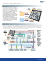
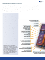
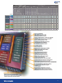
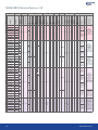
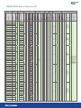
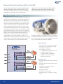
The Core Difference in Your Design
RX600/RX700 Microcontrollers
www.renesas.eu
2015.02
Performance without Sacrifice
The RX architecture is future oriented and feature rich.
It’s driven by a Renesas technology roadmap that
focuses on the global environment and anticipates the
enormous gains in sophistication that microcontrollerbased products are expected to achieve in the next
10 to 20 years. Thus, the RX family of microcontrollers
(MCUs) delivers superior performance in terms of
core processing performance, code efficiency, and
power consumption. An extensive portfolio of onchip mixed-signal peripherals is available, and fast
90 nm/40 nm Flash memory is embedded. That Flash
unleashes full CPU performance, feeding instructions
to the 32-bit RX CPU with no delays – no waits, no
stalls – maintaining the MCU’s peak performance of
480 DMIPS. Memory acceleration isn’t required, and
the result is just pure, predictable performance.
Today designers are confronted with many critical design
and implementation issues. RX MCUs are designed to
solve these issues and help them create new innovative
end-products faster and more easily than in the past.
2
www.renesas.eu
Block Diagram & Features
240 MHz 480 DMIPS
Floating-Point Operation Unit
DSP Instructions
Register Indirect Multiply-and-Accumulate (Result: 80-bit)
Register Direct Multiply-and-Accumulate (Result: 48-bit)
• Design solutions in the RX600 series are scalable. Over
200 products are available now offering
BER O
M
Flash memory from 32 KB to 4 MB
and packages with 48 to 177 pins.
Flash
up to 4 MB
Ethernet Controller
2 ch
SRAM
512 KB
ECC RAM: 32 KB
Standby RAM: 8 KB
IEEE 1588
Clock Synchronisation
Control
USB High-Speed: 1 ch
USB Full-Speed: 1 ch
Clock Generation Circuit
PLL
High-Speed
On-Chip Oscillator
Data Flash
64 KB
Power-On Reset
Voltage Detection Circuit
Encryption/Safety
I2C Bus Interface
x 2 ch
Encryption Modules
AES/DES/SHA/RNG
Serial Communications
Interface x 13 ch
(incl. 4 ch with FIFO)
Event Link
Controller
Timers
Memory Protection
Unit
Register Write
Protection Unit
Multifunction Timer
Pulse Unit (MTU3)
16-bit: 8 ch
32-bit: 1 ch
Clock Frequency
Accuracy
Measurement Circuit
General PWM Timer
(GPT)
CRC Calculator
Timer Pulse Unit
(TPU)
Data Operation Circuit
Programmable Pulse
Generator (PPG)
Watchdog Timer
8-bit: 1 ch
8-bit Timer (TMR)
8-bit: 4 ch
Independent
Watchdog Timer
14-bit: 1 ch
16-bit Timer (CMT) x 2 ch
32-bit Timer (CMTW) x 1 ch
Image Capture
Real-Time Clock
Calendar Function
Parallel Data
Capture Unit
CAN: 3 ch
2 x Serial Peripheral
Interfaces
Quad Serial
Peripheral Interface
SD Host Interface
MMC Host Interface
Serial Sound
Interface
Analog
12-bit A/D: 21 ch
12-bit A/D: 8 ch
12-bit DAC: 2 ch
• Latest RX71M devices describe the
top end of the RX platform. With a
CPU clock frequency of 240 MHz, large
embeded 4 MB Flash and 512 KB RAM
combined with all the connectivity
features these device are ideal for any
gateway requirement.
U
C
Communication
M
Interrupt Control
16 Levels, 16 Pins
Memory
R
System
Data Transfer
Controller
ExDMA Controller x 2 ch
DMA Controller x 8 ch
E
N
NU
Barrel Shifer: 32-bit
• RX MCUs leverage Renesas’ mature 90 nm/40 nm
embedded Flash process, which is currently the fastest
in the industry with a 8.3 ns maximum read access time
and is designed for optimized power consumption all
the way up to full 120 MHz operation.
IE
RX 32-bit CPU (V2 Core)
S U P PL
Renesas is the
number one
MCU supplier
worldwide 1,
with a 30%
market share.
• The companion low-voltage RX200 series are available
since Spring, 2011. These more economical MCUs
operate down to lower voltages (as low as 1.62 V),
consume less power, and come in smaller packages
and memory sizes.
• The RX111 provides the entry level 32-bit performance
devices in small packages with USB and lowest power
consumption not only in active, but also in RTC mode.
• The RX100, RX200 and RX600 share the same CPU
core and integrate many of the same peripherals for
easy migration between the three series.
• RX MCUs come with comprehensive system development
support, including a vast range of easy-to-use boards,
tools, software, middleware, and RTOSs from Renesas
and third-party suppliers, comprising a rich ecosystem
of products for accelerating progress in design cycles
and shrinking time to market.
Temperature Sensor
• Superior Architecture
–– RX CPU Core with FPU and DSP: up to 480 DMIPS,
up to 240 MHz
–– Enhanced Harvard architecture and 5-stage pipeline
–– More than six internal busses
–– Multiple Direct Memory Access control
–– Rapid interrupt response
• Fast Flash
–– Industry’s only 90 nm/40 nm up to 120 MHz
embedded Flash
–– CPU receives instructions with no delays
–– Mature and reliable silicon process
• Power Efficiency
–– 300 µA/MHz, with all peripherals active
–– 1.4 µA RTC Deep Standby (RX631/63N)
–– < 1 mW per DMIPS
–– Extends battery life in portable applications
• Code Efficiency
–– Up to 28% code size savings2 compared to popular
32-bit RISC MCUs on the market
–– Variable-length CISC instructions
–– FPU, DSP and bit manipulation instructions
Footnotes:
1: Source: Gartner 2009 Worldwide Semiconductor Market Share Database,
March 2010 results
2: Source: Renesas internal testing
3
Advanced Design and Integration
RX600 Key Benefits
The latest RXv2 Core marries the speed of a
RISC architecture with the flexibility and code
efficiency of a CISC architecture. The CPU
interacts with the Flash and SRAM through
an enhanced Harvard design. The RXv2 Core
leverages the industry’s fastest Flash
memory, delivering up to 2.0 DMIPS/MHz
and 4.39 CoreMark/MHz without wait states.
Tightly coupled to the RX Core are the FPU,
MAC, and RMPA (Repeat Multiply
Accumulate), which are efficiently driven by
DSP and floating point instructions to meet
the growing demand of DSC (Digital Signal
Controller) type applications.
5-stage
Pipeline
Single
Cycle
IEEE-754
Flash
Instruction Bus
Operand Bus
Enhanced
Harvard
Architecture
SRAM
Instruction Bus
Operand Bus
72-bit MAC
Accuracy
Simultaneous Data Transfers
The RX Core uses a large number of parallel busses to handle simultaneous movement of data between the CPU core,
Flash, SRAM, and peripherals. Six different peripheral busses enable a flexible distribution of slow and fast peripherals
for optimized throughput.
An external bus with an –
independent
DMA Interface
can move data directly from one external device
RX Architecture
System
Example
illustrating
4
independent
plus
2
interleaving
to another external device, such as a graphic frame buffer to a TFT-LCD panel. data transfers.
RX600 MCU
SDRAM
664 Bits INST
64 Bits
z Fetch
Bus
Matrix
32 Bits DATA
Independent
Data Transfers
instructions
Enhanced
Harvard
Architecture
64 Bits
32 Bits
z Transmit
USB data
z Move RGB data
External
Bus Pins
for CPU
32 Bits
External
Bus
Controller
ExDMA
32 Bits
TFT-LCD
Bus
Bridge
Flash
Internal Main Bus 2
32 Bits
External Bus Master
SRAM
Internal Main Bus 1
Bus
Bridge
from external
SDRAM to
TFT-LCD
Interleaving
Data Transfers
z Load ADC
DTC
DMA
Bus Master
Bus Master
CNTL
CNTL
Ethernet DMA
Bus Master
CNTL
values into
SRAM
z Move Ethernet
data packets from
internal SRAM
Multiple Peripheral Busses to Spread Bandwidth Loading
z Timer data
written to
DAC output
CNTL
System Control
DMA, DTC, Interrupts,
Clocks, POR/LVD
Communication
USB, CAN, LIN,
SCI/UART, SPI, I2C
4
Timers
General, Motor Control,
WDT, I-WDT, RTC
Analog
ADC, DAC,
Temp Sensor
GPIO
2K
FIFO
FIFO
2K
Ethernet MAC
www.renesas.eu
Performance
Superior FPU Implementation
The RX Core delivers up to 2.0 DMIPS per MHz, achieving
480 DMIPS when running up to 240 MHz.
The RX FPU implementation allows direct access to general
registers, resulting in faster execution and smaller code size.
• The new RX71M sets new standards in its class with a
4.39 CoreMark/MHz benchmarks. The results being
continually improved with new compiler releases. At the
time of printing, the Renesas RX compiler delivers the
best RX benchmarks, however please contact Renesas
for updated performance figures.
• RX eliminates the overhead of load/store operations
• Results in higher performance and smaller code size
Traditional FPU Implementation
RX FPU Implementation
General
Registers
General
Registers
Load/Store
Dedicated
FPU
Registers
Dhrystone MIPS per MHz
with no wait-state memory access
FPU
FPU
2.0
1.25
Industry’s only 120 MHz On-chip Flash
1.1
0.95
RX600
Cortex™-M4
Cortex™-M3
1.50
1.0
ARM9
ARM7
2.0
Dhrystone 2.1 numbers
for ARM processors taken
from www.arm.com
RX600 with
120 MHz Flash
Processing Performance
1.25
No-wait Flash
Competing MCU
with 30 MHz Flash
1 wait-state
30 MHz
2 wait-states
60 MHz
120 MHz
MCU Frequency
Efficient Interrupt Handling
There are flexible options to achieve minimum latency for
various scenarios:
• Normal interrupt responds in as few as seven CPU clock
cycles from the event until the firmware serves the interrupt.*
• Fast interrupt mode can be assigned dynamically to any
interrupt source, responding in just five CPU clocks, using
dedicated registers to save and restore the CPU state.
• All interrupt service routines can be shortened by
dedicating up to four RX CPU general registers for use
only by interrupts, eliminating the need to push and pop
the registers to and from the stack.
INT Trigger to CPU Core
Normal Interrupt
Save PC,
PSW
to SRAM
CPU
Latency
Save
General Reg
to SRAM
User Code
Restore
General Reg
from SRAM
7 cycles typ.
Restore PC,
PSW
from SRAM
6 cycles typ.
Fast Interrupt
CPU
Latency
Save PC,
PSW
to Reg
Save
General Reg
to SRAM
User Code
5 cycles typ.
Restore
General Reg
from SRAM
Restore
PC, PSW
from Reg
3 cycles typ.
Fast Interrupt with Dedicated General Registers
CPU
Latency
Save PC,
PSW
to Reg
5 cycles typ.
User Code
Restore
PC, PSW
from Reg
3 cycles typ.
*Interrupt priority judgement cycles not included.
Substantial Code Size Reduction
The RX CISC CPU architecture has inherent advantages
over RISC CPUs in terms of code size, with RX’s variable
length instructions ranging from 8 bits to 64 bits, allowing
the compiler to select just the right instruction to do the job.
• Many RISC MCUs have only two instruction lengths,
16 bits and 32 bits, so the compiler must make compromises.
• RX CPU supports 10 addressing modes, which optimize
manipulation and movement of data.
• Compiled RX code has been measured as much as 28%
smaller than the same code compiled on a popular
RISC MCU.
Code Size (relative)*
Motor
Control
28% Less
Data
Communication
19% Less
Data
Conversion
17% Less
Real-time
Control
25% Less
System
Control
25% Less
RX600
Company S Cortex-M3
*Renesas internal testing
5
Highly Effective Power Management
Strike an optimized balance of performance and power
consumption with many low-power modes of operation
enabled by these design techniques:
Run Mode Fully active
300 µA/MHz
Clock Power
• Flexible system clocking and gating for each peripheral
Clocks disabled Sleep Mode
Clock
CPU
OFF
CPU
Peripheral
OFF
Peripheral
SRAM
SRAM
• Selective power domain gating for unused sections
of the device
RTC
RTC
43% Reduction
TY
FU
LI
IN CREASE
Milliwatts per DMIPS*
D
E
E
W POWER
LO
Deep Software Standby Mode
Only RTC running
1.4 µA
• Low-power, high-voltage threshold transistors
minimize leakage
N CTIO N
A
Software Standby Mode
87 µA
SRAM state retained
Clock
Power
Clock
Power
CPU
OFF
OFF
OFF
OFF
CPU
Peripheral
OFF
OFF
OFF
OFF
Peripheral
SRAM
OFF
OFF
OFF
SRAM
RTC
RX600
RTC
2.0
1.0
Company S Cortex-M3 MCU
4 mA
Power
* Derived from IDD specifications
in product datasheets
• Compared to a Cortex-M3 based MCU, an RX600 chip
enables up to a 43% power reduction – consuming
only 1 mW per DMIPS
• The RX Series has four power modes to manage precious
battery energy consumption without compromising
performance
EMC Advantages – Built-in to Eliminate
Immunity Level
Outstanding EMC performance of RX600 MCUs reduces
system-integration problems, lowers development
costs, and shortens design cycles. BOM costs drop, too,
because external components can be eliminated
RX62T
COMPETITION
• Strong electromagnetic immunity boosts system reliability
• Careful VCC and VSS layout
50 V
Very Low
• Noise filters on input signals
150 V
300 V
400 V
Medium
500 V
Very High
“ Langer EMV and Renesas Electronics today announced that the
• Advanced chip layout techniques
RX600 microcontroller (MCU) family is the most robust MCU
Langer EMV has ever tested against environmental noise ”
Renesas press release, October 21, 2010
RX Family Product Portfolio
200
The RX family currently consists of
120/240 MHz, up to 4 MB Flash,
32-BIT MCU
three extensive product series.
Dual Ethernet, Graphics
FAMILY
Controller, I S Audio,
MCUs in the RX600 series are
12-bit ADC, and more...
optimized for applications requiring
100
200+ Products
high-performance, high-efficiency
RX610 RX62N RX631
500 µA/MHz, up to 2 MB Flash,
processors. Devices in the RX200
RX621 RX62T RX63N
Ethernet, USB, CAN, Motor Control RX62G RX630 RX63T
series introduced in 2011 have
expanded the range of compatible
50
system-design choices, adding
RX2
200 µA/MHz, up to 1 MB Flash RX210
RX21A
RX2
24-bit ∆Σ ADC,
smaller, lower power devices with
RX220
RX2
Wide Range 1.62 V – 5.5 V
Low Pin Count
fewer pins. The latest evolutionary
Fast Wake-up
parts of the RX100 series provide
the entry level 32-bit performance
devices in small packages with USB and lowest power
Migration from existing Renesas architectures to RX
consumption not only in active, but also in RTC mode.
solutions is easy. And, of course, moving designs
Max MHz
2
6
www.renesas.eu
among RX family members is very easy, since RX700,
RX600, RX200 and RX100 MCUs share the same CPU
architecture and peripherals. This gives system engineers
RX63N – Q3 2011
RX62N – NOW
valuable designEthernet/USB/CAN
flexibility and Ethernet/USB/CAN
provides substantial head
starts on reusing software assets. New products for
niche markets can be created quickly and efficiently, as
can upgraded or simplified versions of existing products
for addressing changes in customer preferences.
RX62T – NOW
Motor/Inverter
RX63N
120 MHz,
40 nm Technology
240 MHz,
40 nm Technology
RX64M
RX71M
Up to 4 MB Flash
512 KB SRAM
Up to 4 MB Flash
512 KB SRAM
Higher Speed
Connectivity
Higher Speed
Connectivity
Audio Interface
Audio Interface
Higher Precision
Analog
Higher Precision
Analog
Advanced Security
Advanced Security
Advanced Human
Machine Interface
Advanced Human
Machine Interface
And much more...
And much more...
Ethernet
CAN
RX62N
Ethernet
USB
RX631
Motor
Control
RX610
General
Purpose
Connectivity
Graphics
CAN
RX621
CAN
USB
RX630
Graphics
CAN
RX62T
Advanced
Motor Control
CAN
USB
Graphics
USB
RX63T
LIN
RX62G
Motor
Control
CAN
USB
Graphics
General
Purpose
100 MHz, 90 nm Technology
Connectivity
RX600 MCU Series Roadmap
Advanced
Motor Control
CAN
LIN
High Resolution
Timer 312.5 psec/bit
CAN
LIN
RX600 MCU Series Portfolio
General
Purpose
Motor
Control
Connectivity
RX610
RX621
RX62N
RX64M
RX62T
RX630
RX631
RX63N
RX71M
RX63T
DPS
RX62G
4.0 MB
3.0 MB
2.5 MB
2.0 MB
FLASH MEMORY
1.5 MB
1.0 MB
768 KB
512 KB
384 KB
256 KB
Available
in 9 x9 only
128 KB
64 KB
48 KB
32 KB
DEVICE/PINS LQFP48
Body Size
Pitch
7x7
0.5 mm
LQFP64 LQFP80
10 x 10 12 x 12
0.5 mm 0.5 mm
LQFP80
LGA85
LGA100
14 x 14
7x7
5.5 x 5.5
0.65 mm 0.65 mm 0.5 mm
LQFP100
14 x 14
0.5 mm
LQFP112 LQFP120
20 x 20
0.65 mm
16 x 16
0.5 mm
LQFP144
20 x 20
0.5 mm
LGA145
7x7 9x 9
0.5 mm 0.65 mm
BGA176
13 x 13
0.8 mm
LQFP176
24 x 24
0.5 mm
LGA177
8x8
0.5 mm
7
Comprehensive On-chip Peripherals
To save cost, simplify system designs, reduce total
system power consumption, and enable the
implementation of value-added features, a wide range
of on-chip peripheral functions is clustered around the
powerful CPU core of RX MCUs. Broadly categorized into
analog, timer, communication and system functions, these
numerous peripherals are proven designs delivering
impressive performance. The many different types of RX
MCUs offer diverse sets of functions, so chip capabilities
and cost can be matched to application needs. The
devices in the RX621/62N/630/631/63N/64M/71M
and RX62T/63T/62G product groups exemplify this
diversity and optimization.
• RX621/62N/631/63N/64M/71M MCUs
provide extensive communication peripherals
with options for Ethernet, up to three CAN,
and up to two USB-FS 2.0 channels (one
USB-FS and one USB-HS on the RX71M),
each operating as USB Host, USB Device,
or USB OTG (On the Go). Additionally, they
offer up to thirteen SCI, three SPI, and four
I2C serial channels. Among their other
peripherals are analog interfaces; timers;
RTC and POR/LVD functions; and more.
• RX62T/63T MCUs provide improved motor/
inverter control timers and enhanced analog
peripherals for implementing very precise
motor control and positioning applications.
The MTU3 and GPT timer peripherals
enable one MCU to control three motors
simultaneously. An FPU and improved
analog functions make these MCUs ideal
for use with three-shunt or single-shunt
vector-type motor control methods.
• RX630 MCU provides an fantastic General
Purpose feature set making it suitable for
many different applications.
Communication peripherals with up to 3ch
CAN, and USB-FS 2.0 channel operating as
USB Device. Additionally, they offer up to
thirteen SCI, three SPI and four I2C serial
channels. Among their other peripherals
are analog interfaces; timers; RTC and
POR/LVD functions; and more.
• RX62G MCU provides improved high
resolution timer functionality base on the
GPT Timer unit, enable to generate a PWM
signal with 312.5 psec/bit. An FPU and
improved analog functions make these
MCUs ideal solution for Digital Power
Supply designs, where a High Resolution
timer is essential to bring the system
design cost down.
8
www.renesas.eu
Basic Peripheral Set
General
Purpose
Motor
Control
DPS**
1
1
1
6
12
8
4
4
1
1
–
12
–
8
4
4
1
1
QSPI
–
4
SSI
–
8
4
LIN
21
8
SPI
2
2
–
2
–
–
–
1
2
6 8/16/32
1
4
13 8/16/32
3
–
–
–
1
2
6 8/16/32
2
–
–
–
–
SCI
8
–
12
I 2C
512 KB 96 KB 32 KB
–
RTC
2 MB 256 KB 32 KB
–
I-WDT
Yes
WDT
–
–
CMT
Connectivity
–
–
–
TMR
–
8
PPG
–
1
2
TPU
1
1
–
MTU2
3
2
512 KB 96 KB 32 KB
Communication
Temperature Sensor
2
1
–
DAC 12-bit
–
–
ADC 12-bit
RX631
RX62N
–
DAC 10-bit
–
Timers
ADC 10-bit
1
Data Flash
Advanced ADC 12-bit
1
SRAM (max)
Graphics ExDMA
2
Flash (max)
CAN 2.0B
–
Group
Analog
AES
USB 2.0 Host/Device/OTG
RX621
Memory
GPT
Ethernet 10/100 MAC
Connectivity
Security
(Option)
MTU3
Advanced
Motor
ExBus
Advanced Peripherals
RX63N
1
2
3
1
–
–
–
Yes
2 MB 256 KB 32 KB
8
2
21
–
1
6
12
8
4
4
1
1
1
4
13 8/16/32
3
–
–
RX64M
2
2
3
1
–
9
4
Yes
4 MB 512 KB 64 KB
–
–
29
2
1
–
6
8
4
4
1
1
1
2
13 8/16/32
1
–
2
1
RX71M
2
2****
3
1
–
9
4
Yes
4 MB 512 KB 64 KB
–
–
29
2
1
–
6
8
4
4
1
1
1
2
13 8/16/32
2
–
2
1
RX610
–
–
–
–
–
–
–
–
2 MB 128 KB 32 KB 16
2
–
–
–
–
12
8
4
4
1
–
–
2
7
–
–
–
–
RX630
–
1*
3
–
–
–
–
–
2 MB 128 KB 32 KB
8
2
21
–
1
6
12
8
4
4
1
1
1
4
13 8/16/32
3
–
–
–
8/16
RX62T
–
–
1
–
8
8
4
–
256 KB 16 KB 8 KB
12
–
–
–
–
–
–
–
–
4
1
1
–
1
3
–
1
1
–
–
RX63T
–
–
–
–
8
8
4
–
64 KB
–
–
–
–
–
–
–
–
–
4
1
1
–
1
3
–
1
1
–
–
8
RX63T-H
–
1
1
–
8
8
RX62G
–
–
1
–
8
8 4***
* USB device only
**Digital Power Supply
8 KB
8 KB
–
512 KB 48 KB 32 KB 20
2
–
–
–
–
–
–
–
4
1
1
–
2
5
16
2
1
–
–
–
256 KB 16 KB 8 KB
–
–
–
–
–
–
–
–
4
1
1
–
1
3
–
1
1
–
–
***Incl. High Res. Timer
–
****1x USB Full Speed / 1x USB High Speed
9
RX600 MCU Series Devices 1/8
2048 k + 32 k
R5F56107VDFP
1536 k + 32 k
R5F56106VDFP
1024 k + 32 k
R5F56104VDFP
768 k + 32 k
R5F56104VDFP
768 k + 32 k
R5F56218BDBG
512 k + 32 k
R5F56217BDBG
384 k + 32 k
R5F56216BDBG
256 k + 32 k
R5F56218BDLE
512 k + 32 k
R5F56217BDLE
384 k + 32 k
R5F56216BDLE
256 k + 32 k
R5F56218BDFB
512 k + 32 k
R5F56217BDFB
384 k + 32 k
R5F56216BDFB
256 k + 32 k
R5F56218BDFP
512 k + 32 k
R5F56217BDFP
384 k + 32 k
R5F56216BDFP
256 k + 32 k
R5F56218BDLD
512 k + 32 k
R5F56217BDLD
384 k + 32 k
R5F56216BDLD
256 k + 32 k
R5F562N8BDBG
512 k + 32 k
R5F562N8ADBG
512 k + 32 k
R5F562N7BDBG
384 k + 32 k
R5F562N7ADBG
384 k + 32 k
R5F562N8BDLE
512 k + 32 k
R5F562N8ADLE
512 k + 32 k
R5F562N7BDLE
384 k + 32 k
R5F562N7ADLE
384 k + 32 k
R5F562N8BDFB
512 k + 32 k
R5F562N8ADFB
512 k + 32 k
R5F562N7BDFB
384 k + 32 k
R5F562N7ADFB
384 k + 32 k
R5F562N8BDFP
512 k + 32 k
R5F562N8ADFP
512 k + 32 k
R5F562N7BDFP
384 k + 32 k
R5F562N7ADFP
384 k + 32 k
R5F562GAADFH
256 k + 32 k
R5F562GADDFH
256 k + 32 k
R5F562G7ADFH
128 k + 8 k
R5F562G7DDFH
128 k + 8 k
R5F562GAADFP
256 k + 32 k
R5F562GADDFP
256 k + 32 k
R5F562G7ADFP
128 k + 8 k
R5F562G7DDFP
128 k + 8 k
10
128 k 100 3.0 – 3.6 V
7
7
2
–
–
–
–
–
4 22
–
–
1
–
–
–
–
Yes
4x
4ch
–
2ch –
–
–
4 Yes
117
64 k
2
LGA
145-pin
9 x 9 mm
0.65 mm
pitch
96 k
105 2
64 k
6
2
–
Yes SDRAM
96 k
64 k
100 2.7 – 3.6 V 105
1
–
4 16 MTU2
1
1
1
1
2x
or
4ch
2ch
8ch
or
- Yes
– Yes –
LQFP
144-pin
4 Yes 20 x 20 mm
0.5 mm
pitch
LQFP
100-pin
14 x 14 mm
0.5 mm
pitch
74
64 k
2
96 k
6
1
–
–
Yes
1
96 k
–
128
1
64 k
1
105 2
6
2
–
64 k
–
100 2.7 – 3.6 V
1
– Yes 4 16 MTU2
1
96 k
–
105
1
64 k
LGA
145-pin
9 x 9 mm
0.65 mm
pitch
Yes SDRAM
–
1
1
1
1
2x
or
4ch
2ch – Yes –
8ch
or
– Yes
1 Yes
LQFP
144-pin
20 x 20 mm
0.5 mm
pitch
1
–
1
96 k
74
2
6
1
–
64 k
–
–
1
Yes
1
82
1
8k
1
100 4.0 – 5.5 V
16 k
76
LQFP
112-pin
20 x 20 mm
0.65 mm
pitch
–
3
1
1
–
1
–
1
–
–
–
– 14
MTU3
and
GPT
1
1
–
1
–
–
–
–
12ch
2x
4ch
–
6 Yes
- Yes
LQFP
100-pin
14 x 14 mm
0.5 mm
pitch
Other Features
FPU;
DSP RMPA;
Barrel Shifter;
SDRAM
Interface;
Programmable
Pattern
Generator (PPG),
RTC, Ethernet
DMA, CRC Unit
FPU; DSP RMPA;
Barrel Shifter;
Programmable
Pattern
Generator (PPG),
RTC, Ethernet
DMA, CRC Unit
LQFP
100-pin
14 x 14 mm
0.5 mm
pitch
–
16 k
FPU;
DSP RMPA;
Barrel Shifter;
SDRAM
Interface;
Programmable
Pattern
Generator (PPG),
RTC, CRC Unit
BGA
176-pin
13 x 13 mm
0.8 mm
pitch
2
–
96 k
FPU;
DSP RMPA;
Barrel Shifter;
Programmable
Pattern
Generator (PPG)
FPU;
DSP RMPA;
Barrel Shifter;
Programmable
Pattern
Generator (PPG),
RTC, CRC unit
LGA
85-pin
7 x 7 mm
0.65 mm
pitch
60
64 k
8k
–
1
96 k
Qualification
BGA
176-pin
13 x 13 mm
0.8 mm
pitch
96 k
128
LQFP
144-pin
20 x 20 mm
0.5 mm
pitch
Industrial -40°C to 85°C
R5F56108VDFP
140
Industrial -40°C to 85°C
768 k + 32 k
Industrial -40°C to 85°C
RX610
RX621
RX62N
RX62G
R5F56104WDBG
Industrial -40°C to 85°C
BGA
176-pin
13 x 13 mm
0.8 mm
pitch
R5F56107WDBG 1536 k + 32 k
R5F56106WDBG 1024 k + 32 k
Packages
DTC
DMA
Security
POR & LVD
Miscellaneous Information
ProgOpAmp
10-bit DAC
12-bit ADC
Analog
10-bit ADC
External Data Bus
TFT LCD
Parallel I/F
32.768 kHz
HOCO
LOCO
RTC
WDT
Clock
IWDT
Motor
Timer 16-bit
Timer 8-bit
Ethernet
USB Device
Timers
USB (Host/Device/OTG)
CAN
LIN
I 2C
SCI
SPI
Interfaces
I/O
Supply Voltage [V]
Max. Clock Speed [MHz]
Operation
RAM [Byte]
Memory
Flash [Byte]
Group
Part Number
Device
FPU; DSP RMPA;
Barrel Shifter;
External Input
(POE) Windows
Comparator;
Clock Stop
Detection;
Clock Monitoring;
ADC Diagnostic,
CRC Unit;
High Resolution
Timer with
312.5 psec/bit
www.renesas.eu
RX600 MCU Series Devices 2/8
2.7 – 3.6 V
128 k + 8 k
4.0 – 5.5 V
1
R5F562T7EDFH
128 k + 8 k
2.7 – 3.6 V
–
R5F562T7DDFH
128 k + 8 k
4.0 – 5.5 V
–
R5F562TABDFP 256 k + 32 k
2.7 – 3.6 V
1
R5F562TAADFP 256 k + 32 k
4.0 – 5.5 V
1
2.7 – 3.6 V
–
16 k
R5F562TADDFP 256 k + 32 k
4.0 – 5.5 V
–
76
R5F562T7BDFP
128 k + 8 k
2.7 – 3.6 V
R5F562T7ADFP
128 k + 8 k
4.0 – 5.5 V
1
R5F562T7EDFP
128 k + 8 k
2.7 – 3.6 V
–
8k
1
R5F562T7DDFP
128 k + 8 k
4.0 – 5.5 V
–
R5F562TABDFF
256 k + 32 k
2.7 – 3.6 V
1
R5F562TAADFF
256 k + 32 k
4.0 – 5.5 V
1
R5F562TAEDFF
256 k + 32 k
2.7 – 3.6 V
–
R5F562TADDFF
256 k + 32 k
4.0 – 5.5 V
–
R5F562T7BDFF
128 k + 8 k
2.7-3.6 V
1
R5F562T7ADFF
128 k + 8 k
4.0 – 5.5 V
1
R5F562T7EDFF
128 k + 8 k
2.7 – 3.6 V
R5F562T7DDFF
128 k + 8 k
R5F562T6BDFF
64 k + 8 k
R5F562T6ADFF
64 k + 8 k
R5F562T6EDFF
64 k + 8 k
R5F562T6DDFF
64 k + 8 k
16 k
8k
100
57
–
4.0 – 5.5 V
–
2.7 – 3.6 V
1
4.0 – 5.5 V
1
2.7 – 3.6 V
3
1
1
1
–
4.0 – 5.5 V
–
R5F562TABDFM 256 k + 32 k
2.7 – 3.6 V
1
R5F562TAADFM 256 k + 32 k
4.0 – 5.5 V
1
2.7 – 3.6 V
–
R5F562TAEDFM 256 k + 32 k
16 k
R5F562TADDFM 256 k + 32 k
4.0 – 5.5 V
–
R5F562T7BDFM
128 k + 8 k
2.7 – 3.6 V
1
R5F562T7ADFM
128 k + 8 k
4.0 – 5.5 V
R5F562T7EDFM
128 k + 8 k
2.7 – 3.6 V
R5F562T7DDFM
128 k + 8 k
4.0 – 5.5 V
–
R5F562T6BDFM
64 k + 8 k
2.7 – 3.6 V
1
R5F562T6ADFM
64 k + 8 k
4.0 – 5.5 V
1
R5F562T6EDFM
64 k + 8 k
2.7 – 3.6 V
–
R5F562T6DDFM
64 k + 8 k
4.0 – 5.5 V
–
2.7 – 3.6 V
1
4.0 – 5.5 V
1
2.7 – 3.6 V
–
8k
R5F562TABDFK 256 k + 32 k
R5F562TAADFK 256 k + 32 k
R5F562TAEDFK
256 k + 32 k
16 k
57
1
–
R5F562TADDFK 256 k + 32 k
4.0 – 5.5 V
–
R5F562T7BDFK
128 k + 8 k
2.7 – 3.6 V
1
R5F562T7ADFK
128 k + 8 k
4.0 – 5.5 V
R5F562T7EDFK
128 k + 8 k
2.7 – 3.6 V
R5F562T7DDFK
128 k + 8 k
4.0 – 5.5 V
–
R5F562T6BDFK
64 k + 8 k
2.7 – 3.6 V
1
R5F562T6ADFK
64 k + 8 k
4.0 – 5.5 V
1
R5F562T6EDFK
64 k + 8 k
2.7 – 3.6 V
–
R5F562T6DDFK
64 k + 8 k
4.0 – 5.5 V
–
8k
Others features
Packages
DTC
DMA
Security
LQFP
80-pin
14 x 14mm
0.65 mm
pitch
10-bit DAC
– 10
2x
4ch
4ch
TFT LCD
LQFP
100-pin
14 x 14 mm
0.5 mm
pitch
32.768 kHz
2x
4ch
HOCO
12ch
LOCO
– 14
RTC
LQFP
112-pin
20 x 20mm
0.65 mm
pitch
WDT
2x
4ch
IWDT
12ch
Motor
– 14
Qualification
POR & LVD
ProgOpAmp
External Data Bus
Timer 16-bit
Timer 8-bit
Ethernet
1
128 k + 8 k
R5F562T7ADFH
256 k + 32 k
USB Device
–
82
R5F562T7BDFH
R5F562TAEDFP
Miscellaneous Information
46
1
–
–
–
MTU3
and
GPT
–
1
1
–
1
–
–
–
–
–
6 Yes –
Industrial -40°C to 85°C
–
8k
Analog
12-bit ADC
1
2.7 – 3.6 V
4.0 – 5.5 V
Parallel I/F
10-bit ADC
4.0 – 5.5 V
R5F562TADDFH 256 k + 32 k
Clock
1
2.7 – 3.6 V
R5F562TAADFH 256 k + 32 k
16 k
Timers
USB (Host/Device/OTG)
CAN
LIN
I 2C
SCI
SPI
I/O
Interfaces
R5F562TABDFH 256 k + 32 k
R5F562TAEDFH 256 k + 32 k
RX62T
Supply Voltage [V]
Max. Clock Speed [MHz]
Operation
RAM [Byte]
Memory
Flash [Byte]
Part Number
Group
Device
– Yes
– 10
–
2x
4ch
LQFP
64-pin
10 x 10mm
0.5 mm
pitch
– 10
–
2x
4ch
LQFP
64-pin
14 x 14mm
0.8 mm
pitch
FPU; DSP RMPA;
Barrel Shifter;
External Input
(POE) Windows
Comparator;
Clock Stop
Detection;
Clock Monitoring;
ADC Diagnostic;
CRC Unit
11
RX600 MCU Series Devices 3/8
R5F5630ADDFC
768 k + 32 k
R5F56308DDFC
512 k + 32 k
R5F5630EDDBG 2048 k + 32 k
R5F5630DDDBG 1536 k + 32 k
R5F5630BDDBG 1024 k + 32 k
R5F5630ADDBG 768 k + 32 k
R5F56308DDBG
512 k + 32 k
R5F56307DDBG
384 k + 32 k
R5F5630EDDLK 2048 k + 32 k
R5F5630DDDLK 1536 k + 32 k
R5F5630BDDLK 1024 k + 32 k
R5F5630ADDLK
768 k + 32 k
R5F56308DDLK
512 k + 32 k
R5F56307DDLK
384 k + 32 k
RX630
R5F5630EDDFB 2048 k + 32 k
R5F5630DDDFB 1536 k + 32 k
R5F5630BDDFB 1024 k + 32 k
R5F5630ADDFB
768 k + 32 k
R5F56308DDFB
512 k + 32 k
R5F56307DDFB
384 k + 32 k
R5F5630EDDLA 2048 k + 32 k
R5F5630DDDLA 1536 k + 32 k
R5F5630BDDLA 1024 k + 32 k
R5F5630ADDLA 768 k + 32 k
R5F56308DDLA
512 k + 32 k
R5F56307DDLA
384 k + 32 k
R5F5630EDDFP 2048 k + 32 k
R5F5630DDDFP 1536 k + 32 k
R5F5630BDDFP 1024 k + 32 k
R5F5630ADDFP
R5F56308DDFP
512 k + 32 k
R5F56307DDFP
384 k + 32 k
R5F56306DDFP
256 k + 32 k
R5F56308DDFN
512 k + 32 k
R5F56307DDFN
384 k + 32 k
96 k
64 k
1
128 k
3
96 k
133
64 k
3 13 4
128 k
Others features
Qualification
Packages
DTC
DMA
Security
POR & LVD
ProgOpAmp
10-bit DAC
12-bit ADC
10-bit ADC
External Data Bus
TFT LCD
32.768 kHz
HOCO
LOCO
RTC
WDT
IWDT
Motor
Timer 16-bit
Timer 8-bit
Ethernet
USB Device
BGA
176-pin
13 x 13mm
0.8 mm
96 k
22
3
111
21ch 2ch
LGA
145-pin
7 x 7 mm
0.5 mm
2
64 k
1
128 k
3
100 2.7 – 3.6 V
96 k
–
111
–
1
–
4
MTU2 1
1
2
64 k
1
Vbat
1
Anti
Tamper
Yes
1 Yes
8ch
–
– Yes –
4 Yes
LQFP
144-pin
20 x 20 mm
0.5 mm
FPU; DSP
RMPA;
Barrel Shifter;
Programmable
Pattern
Generator
(PPG);
RTC with
Vbat;
CRC Unit;
Temperature
Sensor
FPU; DSP
RMPA;
Barrel Shifter;
External
Input (POE)
Windows
Comparator;
Clock Stop
Detection;
Clock
Monitoring;
ADC
Diagnostic;
CRC Unit
1
128 k
2
LGA
100-pin
5.5 x 5.5 mm
0.5 mm
96 k
64 k
1
78
128k
2
3
2
16
14ch
1ch
2
LQFP
100-pin
14 x 14 mm
0.5 mm
96 k
64 k
1
48 k
64 k
58
2
6
2
1
1
2.7 – 3.6 V
–
48 k
R5F563TEDDFB 512 k + 32 k
100
R5F563TCBDFB 384 k + 32 k
12
LQFP
176-pin
24 x 24 mm
0.5 mm
1
1
R5F563TCDDFB 384 k + 32 k
Miscellaneous Information
2
2.7 – 3.6 V
R5F563TCEDFB 384 k + 32 k
Analog
2
4.0 – 5.5 V
R5F563TCADFB 384 k + 32 k
USB (Host/Device/OTG)
CAN
LIN
I 2C
SCI
SPI
I/O
Supply Voltage [V]
Max. Clock Speed [MHz]
133
R5F563TEADFB 512 k + 32 k
512 k + 32 k
Parallel
I/F
Clock
3
R5F563TEBDFB 512 k + 32 k
R5F563TEEDFB
RX63T
768 k + 32 k
128 k
Timers
Industrial -40°C to 85°C
R5F5630BDDFC 1024 k + 32 k
Interfaces
Industrial -40°C to 85°C
R5F5630EDDFC 2048 k + 32 k
R5F5630DDDFC 1536 k + 32 k
Operation
RAM [Byte]
Memory
Flash [Byte]
Group
Part Number
Device
32 k
4.0 – 5.5 V
2.7 – 3.6 V
110 2
5
2
–
–
1
4.0 – 5.5 V
1
2.7 – 3.6 V
–
4.0 – 5.5 V
–
16
1
–
–
– 14
–
MTU3
and 1
GPT
1
–
1
–
–
–
4ch
Yes 20ch
10ch
2x
2ch 6 Yes –
4ch
LQFP 80-pin
12 x 12 mm
0.5 mm
LQFP
144-pin
4 Yes 20 x 20 mm
0.5 mm
pitch
www.renesas.eu
RX600 MCU Series Devices 4/8
4.0 – 5.5 V
48 k
2.7 – 3.6 V
1
R5F563TEADFA 512 k + 32 k
4.0 – 5.5 V
1
2.7 – 3.6 V
–
R5F563TEDDFA
512 k + 32 k
4.0 – 5.5 V
R5F563TCBDFA 384 k + 32 k
2.7 – 3.6 V
R5F563TCADFA 384 k + 32 k
4.0 – 5.5 V
R5F563TCEDFA
384 k + 32 k
32 k
2.7 – 3.6 V
–
1
R5F563TBADFA 256 k + 32 k
4.0 – 5.5 V
4.0 – 5.5 V
–
R5F563TEBDFH 512 k + 32 k
2.7 – 3.6 V
1
R5F563TEADFH 512 k + 32 k
4.0 – 5.5 V
1
2.7 – 3.6 V
–
4.0 – 5.5 V
R5F563TCBDFH 384 k + 32 k
2.7 – 3.6 V
R5F563TCADFH 384 k + 32 k
R5F563TCEDFH 384 k + 32 k
4.0 – 5.5 V
32 k
100
R5F563TCDDFH 384 k + 32 k
2.7 – 3.6 V
–
2
1
–
4.0 – 5.5 V
–
2.7 – 3.6 V
4.0 – 5.5 V
1
2.7 – 3.6 V
–
4.0 – 5.5 V
512 k + 32 k
2.7 – 3.6 V
R5F563TEADFP 512 k + 32 k
4.0 – 5.5 V
1
2.7 – 3.6 V
–
R5F563TEEDFP
512 k + 32 k
R5F563TEDDFP
48 k
1
4.0 – 5.5 V
–
2.7 – 3.6 V
1
R5F563TCADFP 384 k + 32 k
4.0 – 5.5 V
2.7 – 3.6 V
78
–
R5F563TCADFP 256 k + 32 k
2.7 – 3.6 V
1
R5F563TCADFP 256 k + 32 k
4.0 – 5.5 V
1
2.7 – 3.6 V
–
4.0 – 5.5 V
–
R5F563TCADFP 256 k + 32 k
R5F563T6EDFM
64 k + 8 k
R5F563T5EDFM
48 k + 8 k
R5F563T4EDFM
32 k + 8 k
R5F563T6EDFM
64 k + 8 k
R5F563T5EDFM
48 k + 8 k
R5F563T4EDFM
32 k + 8 k
–
1
–
–
2.7 – 3.6 V
Yes –
LQFP
112-pin
20 x 20 mm
0.65 mm
4 Yes
pitch
32
3
Others features
LQFP
100-pin
14 x 14 mm
0.5 mm
pitch
8ch
1
Qualification
Packages
DTC
DMA
Security
POR & LVD
ProgOpAmp
10-bit DAC
–
48
8k
12-bit ADC
10-bit ADC
External Data Bus
TFT LCD
32.768 kHz
HOCO
LOCO
RTC
IWDT
Motor
Timer 16-bit
WDT
1
–
4.0 – 5.5 V
24 k
1
1
4
R5F563TCADFP 384 k + 32 k
R5F563TCADFP 256 k + 32 k
12ch
1
FPU; DSP
RMPA;
Barrel Shifter;
External
Input (POE)
Windows
Comparator;
Clock Stop
Detection;
Clock
Monitoring;
ADC
Diagnostic;
CRC Unit
1
512 k + 32 k
R5F563TCADFP 384 k + 32 k
MTU3
and
GPT
–
2ch 6
–
R5F563TCBDFP 384 k + 32 k
32 k
–
2x
4ch
Yes
1
R5F563TBDDFH 256 k + 32 k
R5F563TEBDFP
14
–
–
R5F563TBADFH 256 k + 32 k
24 k
1
1
90
R5F563TBBDFH 256 k + 32 k
R5F563TBEDFH 256 k + 32 k
Timer 8-bit
–
R5F563TBDDFA 256 k + 32 k
R5F563TEDDFH 512 k + 32 k
Ethernet
1
5
2.7 – 3.6 V
48 k
USB Device
–
2.7 – 3.6 V
512 k + 32 k
LQFP
120-pin
16 x 16 mm
0.5 mm
pitch
1
93
R5F563TBBDFA 256 k + 32 k
R5F563TEEDFH
LQFP
144-pin
20 x 20 mm
0.5 mm
pitch
1
4.0 – 5.5 V
24 k
Miscellaneous Information
–
2
R5F563TCDDFA 384 k + 32 k
R5F563TBEDFA 256 k + 32 k
USB (Host/Device/OTG)
CAN
LIN
I 2C
SCI
SPI
–
2.7 – 3.6 V
32 k
Analog
20ch
–
512 k + 32 k
512 k + 32 k
Parallel I/F
1
110
4.0 – 5.5 V
R5F563TEEDFA
Clock
1
R5F563TBDDFB 256 k + 32 k
R5F563TEBDFA
Timers
Industrial -40°C to 85°C
2.7 – 3.6 V
R5F563TBADFB 256 k + 32 k
Interfaces
I/O
Supply Voltage [V]
Max. Clock Speed [MHz]
R5F563TBBDFB 256 k + 32 k
R5F563TBEDFB 256 k + 32 k
RX63T
Operation
RAM [Byte]
Memory
Flash [Byte]
Part Number
Group
Device
–
–
16
–
–
–
6ch
–
LQFP
64-pin
10 x 10 mm
0.5 mm
pitch
LQFP
48-pin
7 x 7 mm
0.5 mm
pitch
13
RX600 MCU Series Devices 5/8
512 k + 32 k
384 k + 32 k 128 k
256 k + 32 k
2048 k + 32 k
R5F5631DDDFC 1536 k + 32 k
R5F5631BDDFC
1024 k + 32 k
R5F5631ADDFC
768 k + 32 k
Others features
Qualification
Packages
DTC
DMA
Security
POR & LVD
Miscellaneous Information
ProgOpAmp
10-bit DAC
12-bit ADC
Analog
10-bit ADC
External Data Bus
Parallel I/F
TFT LCD
32.768 kHz
HOCO
LOCO
RTC
WDT
IWDT
Motor
Timer 16-bit
Timer 8-bit
Ethernet
USB Device
USB (Host/Device/OTG)
CAN
LIN
I 2C
Clock
LGA
177-pin
8 x 8 mm
0.5 mm
R5F56317DDLC
R5F5631EDDFC
Timers
128 k
R5F56318DDLC
R5F56316DDLC
SCI
768 k + 32 k
SPI
R5F5631ADDLC
Interfaces
I/O
1024 k + 32 k
Supply Voltage [V]
1536 k + 32 k
R5F5631BDDLC
Max. Clock Speed [MHz]
2048 k + 32 k
Operation
RAM [Byte]
R5F5631EDDLC
R5F5631DDDLC
Group
Flash [Byte]
Memory
Part Number
Device
–
128 k
R5F56318DDFC
512 k + 32 k
R5F56317DDFC
384 k + 32 k 128 k
R5F56316DDFC
256 k + 32 k
R5F5631FHDFC
2048 k + 32 k
R5F5631JHDFC
1536 k + 32 k 256 k
R5F5631YHDFC
1024 k + 32 k
133
2
LQFP
176-pin
24 x 24 mm
0.5 mm
AES
R5F5631KHDFC 2048 k + 32 k
R5F5631GHDFC 1536 k + 32 k 192 k
R5F5631FDDFC
2048 k + 32 k
R5F5631JDDFC
1536 k + 32 k 256 k
R5F5631YDDFC
1024 k + 32 k
R5F5631KDDFC 2048 k + 32 k
100 2.7 – 3.6 V
3 13 4
–
3
–
R5F5631GDDFC 1536 k + 32 k 192 k
–
4 22 MTU2 1
1
1
Vbat
1
Anti
Tamper
1 Yes Yes SDRAM 8ch 21ch 2ch – Yes
Industrial -40°C to 85°C
RX631
R5F5631WHDFC 1024 k + 32 k
4 Yes
R5F5631WDDFC 1024 k + 32 k
R5F5631EDDBG 2048 k + 32 k
R5F5631DDDBG 1536 k + 32 k
R5F5631BDDBG 1024 k + 32 k
128 k
BGA
176-pin
13 x 13 mm
0.8 mm
R5F5631ADDBG 768 k + 32 k
R5F56318DDBG
512 k + 32 k
R5F56317DDBG
384 k + 32 k 128 k
R5F56316DDBG
256 k + 32 k
R5F5631EDDLK
2048 k + 32 k
R5F5631DDDLK 1536 k + 32 k
R5F5631BDDLK
1024 k + 32 k
R5F5631ADDLK
768 k + 32 k
–
128 k
LGA
145-pin
7 x 7 mm
0.5 mm
R5F56318DDLK
512 k + 32 k
R5F56317DDLK
384 k + 32 k 128 k
R5F56316DDLK
256 k + 32 k
R5F5631EDDFB
2048 k + 32 k
R5F5631DDDFB 1536 k + 32 k
R5F5631BDDFB 1024 k + 32 k
R5F5631ADDFB
111
1
128 k
768 k + 32 k
R5F56318DDFB
512 k + 32 k
R5F56317DDFB
384 k + 32 k 128 k
R5F56316DDFB
256 k + 32 k
14
FPU;
DSP RMPA;
Barrel Shifter;
SDRAM
Interface;
Programmable
Pattern
Generator
(PPG);
RTC with Vbat
(177 – 64-pin);
CRC Unit;
Temperature
Sensor
LQFP
144-pin
20 x 20 mm
0.5 mm
www.renesas.eu
RX600 MCU Series Devices 6/8
R5F5631FHDFB
2048 k + 32 k
R5F5631JHDFB
1536 k + 32 k 256 k
R5F5631YHDFB
1024 k + 32 k
R5F5631KHDFB
2048 k + 32 k
R5F5631GHDFB
1536 k + 32 k 192 k
1024 k + 32 k
R5F5631FDDFB
2048 k + 32 k
R5F5631JDDFB
1536 k + 32 k 256 k
1024 k + 32 k
R5F5631KDDFB
2048 k + 32 k
R5F5631GDDFB
1536 k + 32 k 192 k
1024 k + 32 k
2048 k + 32 k
R5F5631DDDFJ
1536 k + 32 k
R5F5631BDDFJ
1024 k + 32 k
R5F5631ADDFJ
768 k + 32 k
R5F56318DDFJ
512 k + 32 k
R5F56317DDFJ
384 k + 32 k
R5F56316DDFJ
256 k + 32 k
R5F5631EDDFP
2048 k + 32 k
R5F5631DDDFP
1536 k + 32 k
R5F5631BDDFP
1024 k + 32 k
R5F5631ADDFP
768 k + 32 k
Others features
Qualification
Packages
DTC
DMA
Security
POR & LVD
Miscellaneous Information
ProgOpAmp
10-bit DAC
12-bit ADC
Analog
10-bit ADC
External Data Bus
Parallel I/F
TFT LCD
32.768 kHz
HOCO
LOCO
RTC
Clock
WDT
IWDT
Motor
Timer 16-bit
Timer 8-bit
Ethernet
USB Device
Timers
USB (Host/Device/OTG)
CAN
LIN
I 2C
SCI
SPI
I/O
Supply Voltage [V]
111
R5F5631YDDFB
R5F5631EDDFJ
Interfaces
AES
R5F5631WHDFB
R5F5631WDDFB
Max. Clock Speed [MHz]
Operation
RAM [Byte]
Flash [Byte]
Part Number
Memory
3 13 4
3
SDRAM
22
LQFP
144-pin
20 x 20 mm
0.5 mm
21ch
128 k
LGA
100-pin
7 x 7 mm
0.65 mm
–
128 k
Yes
128 k
100 2.7 – 3.6 V
R5F56318DDFP
512 k + 32 k
R5F56317DDFP
384 k + 32 k
R5F56316DDFP
256 k + 32 k
R5F5631FHDFP
2048 k + 32 k
R5F5631JHDFP
1536 k + 32 k 256 k
R5F5631YHDFP
1024 k + 32 k
R5F5631KHDFP
2048 k + 32 k
R5F5631GHDFP
1536 k + 32 k 192 k
128 k
1
–
78
9
2
–
–
4
MTU2 1
1
1
Vbat
1
Anti
Tamper
2ch
1 Yes
– Yes
Yes
2
2
8ch
4 Yes
14ch
16
AES
R5F5631WHDFP
1024 k + 32 k
R5F5631FDDFP
2048 k + 32 k
R5F5631JDDFP
1536 k + 32 k 256 k
R5F5631YDDFP
1024 k + 32 k
R5F5631KDDFP
2048 k + 32 k
R5F5631GDDFP
1536 k + 32 k 192 k
R5F5631WDDFP
1024 k + 32 k
R5F5631PDDFM
512 k + 32 k
R5F5631NDDFM
384 k + 32 k
R5F5631MDDFM
256 k + 32 k
R5F5631PDDFL
512 k + 32 k
R5F5631NDDFL
384 k + 32 k
R5F5631MDDFL
256 k + 32 k
Industrial -40°C to 85°C
RX631
Group
Device
FPU;
DSP RMPA;
Barrel Shifter;
SDRAM
Interface;
Programmable
Pattern
Generator
(PPG);
RTC with Vbat
(177 – 64-pin);
CRC Unit;
Temperature
Sensor
LQFP
100-pin
14 x 14 mm
0.5 mm
–
64 k
42
12ch 1ch
6
64 k
30
1
1
–
–
LQFP
64-pin
10 x 10 mm
0.5 mm
–
8ch
–
LQFP
48-pin
7 x 7 mm
0.5 mm
15
RX600 MCU Series Devices 7/8
R5F563NEDDLC
2048 k + 32 k
R5F563NDDDLC
1536 k + 32 k
R5F563NBDDLC
1024 k + 32 k
R5F563NADDLC
768 k + 32 k
R5F563NEDDFC
2048 k + 32 k
R5F563NDDDFC
1536 k + 32 k
R5F563NBDDFC
1024 k + 32 k
768 k + 32 k
R5F563NJHDFC
1536 k + 32 k 256 k
R5F563NYHDFC
1024 k + 32 k
R5F563NKHDFC
2048 k + 32 k
R5F563NGHDFC
1536 k + 32 k 192 k
1024 k + 32 k
R5F563NFDDFC
2048 k + 32 k
R5F563NJDDFC
1536 k + 32 k 256 k
R5F563NYDDFC
1024 k + 32 k
R5F563NKDDFC
2048 k + 32 k
R5F563NGDDFC
1536 k + 32 k 192 k
R5F563NWDDFC
1024 k + 32 k
R5F563NEDDBG
2048 k + 32 k
R5F563NDDDBG
1536 k + 32 k
R5F563NBDDBG
1024 k + 32 k
R5F563NADDBG
768 k + 32 k
R5F563NEDDLK
2048 k + 32 k
R5F563NDDDLK
1536 k + 32 k
R5F563NBDDLK
1024 k + 32 k
R5F563NDDDFB
1536 k + 32 k
R5F563NBDDFB
1024 k + 32 k
Others features
Qualification
Packages
DTC
DMA
Security
POR & LVD
Miscellaneous Information
ProgOpAmp
10-bit DAC
12-bit ADC
Analog
10-bit ADC
External Data Bus
TFT LCD
32.768 kHz
HOCO
LOCO
RTC
WDT
IWDT
Motor
Timer 16-bit
Timer 8-bit
Ethernet
USB Device
USB (Host/Device/OTG)
CAN
LIN
I 2C
SCI
SPI
I/O
Supply Voltage [V]
Parallel I/F
LGA
177-pin
8 x 8 mm
0.5 mm
AES
R5F563NWHDFC
768 k + 32 k
Clock
128 k
2048 k + 32 k
2048 k + 32 k
Timers
–
R5F563NFHDFC
R5F563NEDDFB
Interfaces
128 k
R5F563NADDFC
R5F563NADDLK
Max. Clock Speed [MHz]
Operation
RAM [Byte]
Flash [Byte]
Memory
133
LQFP
176-pin
24 x 24 mm
0.5 mm
2
3
128 k 100 2.7 – 3.6 V
2 13 4
–
–
1
4 22 MTU2 1
1
1
Vbat
1
Anti
Tamper
1 Yes Yes SDRAM 8ch 21ch 2ch – Yes
4 Yes
–
BGA
176-pin
13 x 13 mm
0.8 mm
LGA
145-pin
7 x 7 mm
0.5 mm
128 k
Industrial -40°C to 85°C
RX63N
Group
Part Number
Device
FPU;
DSP RMPA;
Barrel Shifter;
SDRAM
Interface;
Programmable
Pattern
Generator
(PPG);
RTC with Vbat;
Ethernet DMA;
CRC Unit,
Temperature
Sensor
128 k
R5F563NADDFB
768 k + 32 k
R5F563NFHDFB
2048 k + 32 k
R5F563NJHDFB
1536 k + 32 k 256 k
R5F563NYHDFB
1024 k + 32 k
R5F563NKHDFB
2048 k + 32 k
R5F563NGHDFB
1536 k + 32 k 192 k
R5F563NWHDFB 1024 k + 32 k
R5F563NFDDFB
2048 k + 32 k
R5F563NJDDFB
1536 k + 32 k 256 k
R5F563NYDDFB
1024 k + 32 k
R5F563NKDDFB
2048 k + 32 k
R5F563NGDDFB
1536 k + 32 k 192 k
111
1
AES
LQFP
144-pin
20 x 20 mm
0.5 mm
2
–
R5F563NWDDFB 1024 k + 32 k
16
www.renesas.eu
RX600 MCU Series Devices 8/8
2048 k + 32 k
R5F563NDDDFJ
1536 k + 32 k
R5F563NBDDFJ
1024 k + 32 k
768 k + 32 k
R5F563NEDDFP
2048 k + 32 k
R5F563NDDDFP
1536 k + 32 k
R5F563NBDDFP
1024 k + 32 k
R5F563NADDFP
768 k + 32 k
R5F563NFHDFP
2048 k + 32 k
R5F563NJHDFP
1536 k + 32 k 256 k
R5F563NYHDFP
1024 k + 32 k
–
128 k
100 2.7 – 3.6 V 76
2
3
2
–
2
1
–
1
4 16 MTU2 1
1
1
Vbat
1
Anti
Tamper
1 Yes Yes
Yes
8ch 14ch 2ch – Yes
4 Yes
AES
R5F563NKHDFP 2048 k + 32 k
1536 k + 32 k 192 k
LQFP
100-pin
14 x 14 mm
0.5 mm
FPU;
DSP RMPA;
Barrel Shifter;
SDRAM
Interface;
Programmable
Pattern
Generator
(PPG);
RTC with Vbat;
Ethernet DMA;
CRC Unit,
Temperature
Sensor
FPU;
DSP RMPA;
Barrel Shifter;
SDRAM
Interface;
Programmable
Pattern
Generator
(PPG);
RTC with Vbat;
Ethernet DMA;
CRC Unit,
Temperature
Sensor;
Trusted Memory;
QSPI; SSI;
Camera I/F PDC;
SDHI I/F optional
R5F563NWHDFP 1024 k + 32 k
R5F563NFDDFP
2048 k + 32 k
R5F563NJDDFP
1536 k + 32 k 256 k
R5F563NYDDFP
1024 k + 32 k
–
R5F563NKDDFP 2048 k + 32 k
R5F563NGDDFP
Others features
Qualification
Packages
DTC
DMA
LGA
100-pin
7 x 7 mm
0.65 mm
128 k
R5F563NADDFJ
R5F563NGHDFP
Security
POR & LVD
Miscellaneous Information
ProgOpAmp
10-bit DAC (12-bit RX64M)
12-bit ADC
Analog
10-bit ADC
External Data Bus
Parallel I/F
TFT LCD
32.768 kHz
HOCO
LOCO
RTC
Clock
WDT
IWDT
Motor
Timer 16-bit
Timer 8-bit
Ethernet
USB Device
Timers
USB (Host/Device/OTG)
CAN
LIN
I 2C
SCI
SPI
I/O
Supply Voltage [V]
Max. Clock Speed [MHz]
Interfaces
Industrial -40°C to 85°C
R5F563NEDDFJ
Operation
RAM [Byte]
Flash [Byte]
Part Number
Memory
Industrial -40°C to 85°C
RX63N
Group
Device
1536 k + 32 k 192 k
R5F563NWDDFP 1024 k + 32 k
R5F564MLCDLC
4096k + 64k
R5F564MJCDLC
3072k + 64k
R5F564MGCDLC 2560k + 64k
R5F564MFCDLC
2048k + 64k
R5F564MLCDFC
4096k + 64k
R5F564MJCDFC
3072k + 64k
R5F564MGCDFC 2560k + 64k
R5F564MFCDFC
LGA
177-pin
8 x 8 mm
0.5 mm
512 k
512 k
128
2
–
LQFP
176-pin
24 x 24 mm
0.5 mm
2
2048k + 64k
R5F564MLCDBG 4096k + 64k
R5F564MJCDBG 3072k + 64k
R5F564MGCDBG 2560k + 64k
512 k
1 13
3
SDRAM
BGA
176-pin
13 x 13 mm
0.8 mm
29ch 2ch
RX64M
R5F564MFCDBG 2048k + 64k
R5F564MLCDLK
4096k + 64k
R5F564MJCDLK
3072k + 64k
R5F564MGCDLK 2560k + 64k
R5F564MFCDLK
512 k 120 2.7 – 3.6 V
2048k + 64k
R5F564MGCDFB 2560k + 64k
–
4 22
4096k + 64k
R5F564MJCDLJ
3072k + 64k
R5F564MGCDLJ 2560k + 64k
R5F564MFCDLJ
2048k + 64k
R5F564MLCDFP
4096k + 64k
R5F564MJCDFP
3072k + 64k
R5F564MGCDFP 2560k + 64k
R5F564MFCDFP
1
1
Vbat
1
Anti
Tamper
1 Yes Yes
–
– Yes
Optional
(AES,
DES,
8 Yes
SHA,
RNG)
LGA
145-pin
7 x 7 mm
0.5 mm
LQFP
144-pin
20 x 20 mm
0.5 mm
512 k
R5F564MFCDFB 2048k + 64k
R5F564MLCDLJ
MTU3
and 1
GPT
112
R5F564MLCDFB 4096k + 64k
R5F564MJCDFB 3072k + 64k
3
1
–
1
LGA
100-pin
7 x 7 mm
0.65 mm
512 k
79
1
9
2
512 k
Yes
22ch 1ch
LQFP
100-pin
14 x 14 mm
0.5 mm
2048k + 64k
For the RX71M part names please refer to the latest RX71M Hardware Manual.
17
Design Potential and Versatility of the RX
System design versatility, application capability, and
economic sensibility are built into the many microcontrollers in the RX family. Driven by a technology
roadmap that anticipates more sophisticated
applications in the next decade that demand cost
effectiveness, RX devices offer abundant core
performance and extensive peripheral functions.
RX62T/RX63T for Motor Control
High-performance CPU and FPU capability, and advanced
analog and timer peripherals, make the RX62T/RX63T an
ideal solution for inverter and motor control applications.
Renesas can help you develop your motor control solution
with kits and firmware that support many kinds of motor
control, including ultra-quiet, energy-efficient, and highprecision three-phase sensorless vector control. In the
home appliance example shown here, the RX62T/RX63T
is driving two three-phase motors simultaneously using its
advanced PWM timers. These timers are well suited for
Brushless DC three-phase motors by having complimentary
PWM outputs with automatic dead-time insertion, an
emergency “Shut-down” (stop) input, and quadrature
encoder inputs for speed and direction feedback. The
RX62T/RX63T’s advanced analog subsystem with multiple
sample-hold circuits enables sampling of three simultaneous
current measurements. It also offers programmable
operational amplifiers and integrated window comparators
to eliminate external components. The 12-bit ADCs have a
fast 1 µsec conversion time, can be triggered by the PWM
timers, and provide self-diagnostic capability.
Advanced Analog
• Two 12-bit ADC units, each with 4 input
channels, 1 μsec conversion time and
self-diagnostic capability
GPIO
Timer
Timers
Timer
Analog
Analog
CAN
Analog
RX62T/RX63T
12-bit ADC S/H
PGA
Detection Circuit
Comp
PWM Generation
Motor
Current
3
PWM Output
6
PWM Interrupt
12-bit ADC S/H
PGA
Detection Circuit
Comp
PWM Generation
PWM Interrupt
Fault Signal
Motor
Current
3
PWM Output
6
Fault Signal
• Each 12-bit ADC unit has
–– 3 x independent sample-hold circuits
–– 3 x programmable op amps
–– 3 x analog window comparators
–– 3 trigger sources (PWM timers,
external and software)
Advanced Timers
• 100 MHz, 16-bit Multifunction Timer Unit
(MTU3)
• 100 MHz, 16-bit General Purpose Timer
Unit (GPT)
• Complimentary PWM and ResetSynchronous outputs
• Dead-time insertion
• Quadrature encoder inputs
• Emergency motor “Shut-down” (stop)
input
18
www.renesas.eu
RX for Connectivity
RX MCUs provide built-in hardware for implementing
efficient communications with external peripherals, systems,
test equipment and networks such as the Internet. The
Ethernet, USB and CAN connectivity modules are wellproven, reliable designs.
Ethernet MAC
• Up to 2ch 10/100 MAC
• 2 KB TX FIFO
• 2 KB RX FIFO
• MII, RMII connection to PHY
• Wake on LAN
RX62N/RX63N/RX64M/RX71M
USB
• Host/Device/OTG
Analog
• High Speed and Full Speed
USB Host
GPIO
• 12 Mbps/480 Mbps
• Up to 2 ports
Internet
Ethernet
CAN
TFT-LCD
• 2 KB FIFO
USB Device
CAN
• ISO11898-1
• 1 Mbps
• 32 Mailboxes
SPI/SCI
ExDMA
• 10 Endpoints
Field
Updates
Expansion
Module
WiFi
Diagnostic
Testing
• Up to 3 channels
SPI/SCI
• Up to 18 MHz (SPI Master)
• Flexible configurations
RX for TFT-LCD Applications
The external DMA controller integrated into RX devices can
drive a TFT-LCD panel directly, greatly reducing the load
on the MCU’s CPU; thus, maximizing the performance of
application software
External DMA Controller
• Directly drive a TFT-LCD panel
• RGB pixel data moves directly
from frame buffer to the TFT-LCD
and never enters the RX MCU
• RX CPU is loaded only 5%, while
refreshing at 60 Hz
• Plenty of CPU bandwidth remains to
run the application, communication
channels, and create moderate
animation on the TFT-LCD
Data
RX621/RX62N
RX631/RX63N
RX64M
USB Host,
OTG, Device
Ethernet
R GB
External
DMA
Controller
WQVGA with
Touch Screen
CAN
Analog
GPIO
Frame Buffer Memory
(SDRAM, SRAM, or PSRAM)
Timer
Clocks
19
Get up and running with the RX Ecosystem
Renesas makes it easy to launch new system designs.
And our comprehensive range of hardware and
software tools – including very low cost and free
products – helps swiftly advance the product
development process from concept stage to final
RX-based design.
System Development Kits
• The Renesas Starter Kit (RSK) facilitates in-depth MCU experimentation and allows system design development
Renesas RX Starter Kit (RSK)
• This complete RX600-based hardware/software
platform for in-depth application design includes the E1
Debugger, a trial version of the e2studio IDE, and
demonstration firmware.
• The kit includes sample code supporting the different
peripheral function.
Processor RSK Part Number
RX610R0K556100S000BE
RX62NR0K5562N0S000BE
RX62TR0K5562T0S000BE
RX630R0K505630S000BE
RX63NR0K50563NS000BE
RX63TR0K50563TS000BE
RX63T-HR0K5563THS000BE
RX62GR0K50562GS000BE
RX64MYR0K50564MS000BE
• The RSKs are specifically designed to be both an
evaluation and development system. The kit includes
everything that an engineer needs to be up and running
within only a few minutes.
• The single installer prepares the target PC with a
comprehensive development environment including
trial C/C++ compiler, editor, build manager and full
source level debugger. A full set of peripheral sample
code gives the user an excellent kick start to their
project development.
Application Development Tools
RX MCUs are supported by a comprehensive set of popular
Renesas hardware and software tools that have been widely
praised for their capabilities and ease of use. Additional
support is provided by a dedicated community of third-party
experts offering many helpful, time-saving products and
services, including the development environments and
optimized compilers from KPIT Cummins (GNURX) and IAR.
In addition the Renesas C++ compiler allows unlimited
binary output size for 60 days; thereafter, restricting compile
size to 128 KB.
Compiler Options
Complete Debugging, Emulation, and Programming
On-chip debugging of an RX-based application is performed
via JTAG connection to the target and USB connection
Renesas E1
R0E000010KCE00
20
to the Windows-based IDE. E1 and J-Link offer thorough
CPU control and visibility. E20 adds high-speed tracing.
Renesas E20
R0E000200KCT00
SEGGER
J-Link
www.renesas.eu
e2studio
Based on the popular open source Eclipse environment,
e2studio offers a complete integrated development
environment based on the free of charge GNU, IAR or
Renesas RX compilers. When the powerful project
management and editor features of the Eclipse
environment are used with the integrated debugging
interface e2studio becomes
everything you need for
embedded RX development.
Can be downloaded free of
charge or purchased as part
of a compiler package.
Part Number: YRX-E2STUDIO-1U
Support Software
Renesas Software Library
Renesas offers a wide variety of free sample code and
libraries supporting applications using Ethernet, USB, CAN,
DSP, Motor Control, PCM Audio and Graphics. Renesas
also provides the Renesas Peripheral Driver Library (RPDL)
and the Peripheral Driver Generator (PDG) free of charge.
GRAPHICS
PCM
AUDIO
CAN
MOTOR
CONTROL
USB
DSP
LIBRARY
TCP/IP
MCU
RSPI
I/O
SCI
CGC
DTC
GPT
WDT
CRC
ADC
DAC
I2C
PFC
BSC
ExDMA
Renesas Peripheral Device Generator (PDG)
• A Windows user interface for configuring RX peripherals
and pins
• Menus to select/initialize peripherals
• Generates C code calls to RPDL driver functions
• Select and manage pin assignments
RTOS
LVD
iAnywhere
CMX Systems
4
4
4
4
Micrium
4
4
4
4
4
SEGGER
4
4
4
4
4
FreeRTOS
4
Express Logic
4
4
4
Sciopta
4
Redpine Signals
4
4
4
4
4
4
IXXAT
4
HCC embedded
4
4
4
TMG
4
4
4
Gainspan
Sevenstax
IS2T
4
4
port
Wittenstein
4
4
Thesycon
Peripheral
P
Driver
Generator
or
4
Java
TPU
DMAC
Profinet
CMT
Interrupt
Powerlink
PWM
Ethercat
PPG
CANopen
MTU
BlueTooth
RPDL Drivers
TMR
Wi–Fi
Timers
Graphic SW
RX600 devices are well suited for embedded real time
tasks, high computation, as well as simultaneous data
transfers on many high-speed communication channels.
Because of this, communication middleware and Real
Time Operating Systems (RTOS) are commonly needed.
Renesas has established technology partnerships with
many leading independent suppliers to provide highquality, cost-effective solutions.
File System
Low-level firmware drivers for all basic RX peripherals are
free, source code included. RPDL eliminates the need for
creating your drivers, saving time and reducing errors.
RPDL functions are easily integrated into HEW projects, and
PDG can be used to generate initialization code and calls to
RDPL functions based on your own specified configuration.
TCP/IP Stack
Third-party RTOS and Middleware
USB Stack
Renesas Peripheral Driver Library (RPDL)
4
4
4
21
Solution Kits for RX
RX Direct-drive Solutions for TFT-LCD
Renesas RX62N RPB Board
A quick and easy solution to add colour
TFT-LCD to your design
RX62N Webserver Demo kit with outstanding test routines
you could do via network
• HTML file hosting
• FPU function test by bouncing
ball and Mandelbrot calculation
• DMIPS MCU benchmark
• “Pong” Mini game
• Features
• Real-Time IEEE-1588 Ethernet PHY
• USB device port
• Mini Joystick
• Low-cost 32-bit MCU solution to drive colour TFT-LCD
panels up to WQVGA resolution
• Only 5% loading on CPU when refreshing the TFT-LCD
panel at 60 Hz, with ample bandwidth left for running
the rest of the application
• Connection port for fast prototyping
Development Environment
• Renesas HEW IDE
• Built-in SEGGER J-Link Lite debugger
• Demo Source code and libraries
• Free graphics API library and examples for evaluating
graphics
Part Number:
YRPBRX62N
(Contact your sales channel
for availability)
• Third-party support for additional graphics requirements
Part Numbers:
YLCDRSKRX62NS (Processor RX62N)
YDISPLAY-IT-RX (Processor RX63N)
Motor Control Solutions Using the RX MCU
A solid evaluation and development platform for motor control
Renesas Demonstration Board (RDK)
for Seminar purpose
This board plugs into a PC’s USB port to showcase the
features and capabilities of RX600 MCUs
• Auto tune & calibrate
• RX MCU board with J-Link integrated debugger and
huge peripheral set, including
Ethernet, CAN and USB
• Sensor/sensorless
• Graphic display
• Ability to drive 2 motors
• 3-axis accelerometer
• Royalty free source code
• Audio in/out
• BLAC motor up to 48 V
• Board will be supplied
during hands-on sessions
seminars
Features
• PC control GUI
• Full schematics
• Installation CD containing:
–– High-performance Embedded Workshop (HEW)
–– RX Family C/C++ toolchains (Renesas 128 KB
evaluation version, full GNU version)
–– Quick-start guide, sample projects
• Tune & calibrate tutorial
Kit content
• Inverter board
• 24 V BLAC motor
• Quick start guide
• CD-ROM including full source code, Gerber files,
schematics, user manual, tutorial & more
Part Numbers:
YRDKRX62N (Processor RX62N)
YRDKRX63N (Processor RX63N)
(Contact your sales channel for
the next seminar in your area)
Part Number:
YROTATE-IT-RX62T
22
www.renesas.eu
Functional Safety Solution according IEC61508-2010 (2nd Edition)
The number of embedded systems with functional safety
requirements is steadily growing. Components with a
safety certification have a clear advantage, they support
the system safety developer with all necessary information
on how to include the component and provide the required
evidences for the claimed safety integrity level (SIL).
To enable a seamless integration into safety applications,
a qualification package for the RX63N/631 microcontroller
series is available. It includes a safety manual containing
the results from a comprehensive analysis based on each
function part of the microcontroller, and all relevant
information and procedures related to functional safety.
A high quality diagnostic software library for the CPU core,
for RAM and Flash is provided. The diagnostic coverage of
the CPU core is proven by fault simulation tests. The
qualification package is certified by the TÜV Rheinland to
ensure compliance to the standard.
Applications
• Industrial Motor Drives
• Safety Controllers
• High quality RX CPU core self-test, diagnostic coverage
proven by fault simulation tests
• Programmable Logic Controllers
• Diagnostic SW developed for IEC61508 SIL3
• Safety Sensors
• Applicable to all part numbers of the RX63N/RX631
product groups
Key Benefits
• Certificate from TÜV Rheinland
• MCU Safety Manual with relevant information to
functional safety
• IEC61508 compliant IAR Embedded Workbench for RX
• Diagnostic SW library containing test routines for RX
CPU core, RAM, and ROM
SIL2 enabled
with one RX63N/631 MCU
Safety Manual
RX63N/631
Safety
Solution
SIL3 enabled
with two RX63N/631 MCUs
Master
CrossMonitoring
Diagnostic SW Library
Watchdog
Certificate from TÜV Rheinland
(compliance to IEC61508 : 2010)
Safety Solution Scheme
Solution Packages
• Renesas Starter Kit+ for RX63N
Functional Safety Production License
• Diagnostics library for CPU, RAM, and ROM
• Diagnostics library for CPU, RAM, and ROM
(Source Code)
• Diagnostics Software User Guide
• Diagnostics Software User Guide
• Safety Manual Evaluation Version
• Safety Manual Full Version
• IAR Installer EWRX-FS v2.42.4 (Evaluation Version)
• Certificate & Test Report from TÜV Rheinland
• Quick Start Guide
• Video
Order Code
• YCERTIFY-IT-RX63N-EV
• YCERTIFY-IT-RX63N-PR
23
RX is Online – www.renesas.eu/rx
Renesas makes product data, design and application
information, and much more available 24/7 in the RX area of
our website. Bookmark it and visit it often to get the latest
data on the newest and previously released devices, learn
details about (and download free versions of) system
development tools, use time-saving MCU-selection aids,
participate in discussion forums, find out about upcoming
events, take advantage of special promotions, and more.
23
INTERACTIVE
INTERACTIVE
Additional Renesas MCU Support
INTERACTIVE
The Alliance Partner Program
allows you to connect instantly
with hundreds of qualified
design consulting and
contracting professionals.
www.renesas.eu/alliance
For educators and students.
Teach with professional grade
tools.Learn MCUs with a
modern architecture.
Gain the technical knowledge
you need. Research and learn at
your own pace, where you want,
when you want, for free.
Gathering place for
technical information on
Renesas MCUs and MPUs.
INTERACTIVE
www.renesasuniversity.com
www.renesas.interactive.com
www.renesasrulz.com
Before purchasing or using any Renesas Electronics products listed herein, please refer to the latest product manual and/or data sheet in advance.
www.renesas.eu
© 2015 Renesas Electronics Europe.
All rights reserved. Printed in Germany.
Document No. R01CL0015ED0900