1
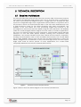
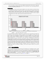
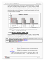
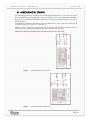
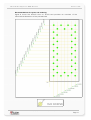
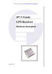
THIS DOCUMENT IS AVAILABLE AT HTTP://WWW.FALCOM.DE/ JP14-R / JP14-Q GPS-Receivers Lead-free products Hardware description Version 1.0.5; Updated: 25/09/2007 JP14-R /JP14-Q FALCOM GPS RECEIVERS VERSION 1.0.5 Table Of Contents 1 INTRODUCTION ........................................................................6 1.1 General ................................................................................................................6 1.2 Used abbreviations ..............................................................................................7 1.3 Related documents ..............................................................................................8 2 SECURITY .................................................................................9 2.1 General information ..............................................................................................9 2.2 Restricted use ......................................................................................................9 2.3 Children ................................................................................................................9 2.4 Operation/antenna ...............................................................................................9 2.5 Electrostatic Discharge (ESD) ..............................................................................9 3 SAFETY STANDARDS ............................................................10 4 TECHNICAL DATA ..................................................................11 4.1 FEATURES ........................................................................................................11 5 TECHNICAL DESCRIPTION ...................................................12 5.1 Receiver Architecture .........................................................................................12 5.2 Product applications ...........................................................................................13 5.3 Technical specifications .....................................................................................13 5.3.1 Electrical Characteristics ...............................................................................................13 5.3.1.1 General .........................................................................................................................................13 5.3.1.2 Accuracy .......................................................................................................................................13 5.3.1.3 DGPS Accuracy ............................................................................................................................13 5.3.1.4 Datum ...........................................................................................................................................13 5.3.1.5 Time to First Position ....................................................................................................................13 5.3.1.6 Sensitivity * ...................................................................................................................................14 5.3.1.7 Dynamic Conditions .....................................................................................................................14 5.3.1.8 DC Power .....................................................................................................................................14 5.3.1.9 Serial Port .....................................................................................................................................14 5.3.1.10 Time – 1PPS Pulse ....................................................................................................................14 5.4 Power management modes overview ...............................................................15 5.4.1 Normal Operation mode ...............................................................................................15 5.4.2 Adaptive TricklePower mode (ATP) ...............................................................................15 5.4.3 Push-to-Fix Mode .........................................................................................................16 5.4.4 NMEA input message for ATP & PTF Mode ..................................................................17 6 HARDWARE INTERFACE AND CONFIGURATION SIGNALS .................................................................................................19 6.1 Interfaces (balls assignment) of the JP14-R .......................................................19 6.2 Interfaces (balls assignment) of the JP14-Q ......................................................20 6.3 Configuration and timing signals ........................................................................21 6.4 Serial communication signals .............................................................................21 6.5 DC input signals .................................................................................................22 7 SOFTWARE INTERFACE .......................................................23 This confidential document is the property of FALCOM and may not be copied or circulated without permission. Page 2 JP14-R /JP14-Q FALCOM GPS RECEIVERS VERSION 1.0.5 7.1 SiRF binary data message .................................................................................23 7.2 NMEA data message .........................................................................................24 7.2.1 NMEA output messages ................................................................................................24 7.2.2 NMEA input messages ..................................................................................................24 7.2.3 Transport Message ........................................................................................................25 8 MECHANICAL DRAW .............................................................26 9 LAYOUT RECOMMENDATION ...............................................29 9.1 Ground planes ....................................................................................................29 9.2 RF connection ....................................................................................................29 9.3 Soldering profile .................................................................................................30 10 FIRST STEPS TO MAKE IT WORK ......................................31 11 APPENDIX .............................................................................33 11.1 How to set the target GPS receiver into power saving modes? ........................33 This confidential document is the property of FALCOM and may not be copied or circulated without permission. Page 3 JP14-R /JP14-Q FALCOM GPS RECEIVERS VERSION 1.0.5 Version history: Version 1.0.0 Author Changes Release date F. Beqiri Initial version 26/07/2005 1.0.1 F. Beqiri - The JP14-Q is a 40-pin BGS package (instead of 36-pin BGA package on the early version). Due to this reason, the following figures and tables are updated (figures 2, 3 and 4 attached; Table 2 – balls 37, 38, 39 and 40 added). - Table 1 updated (JP14-R - balls 13, 14, 15 and 17 changed from GND to NC – not connected). - The diagram of the reflow soldering conditions added. 12/10/2005 1.0.2 F. Beqiri - Corrected round ball diameter from 0.6 mm to 1 mm (see figures 6 and 7). - Corrected sensitivity of the JP14 GPS receivers (see chapter 5.3.1.6, page 14). 09/01/2006 1.0.3 F. Beqiri - Chapter 5.4 on page 15 added. The description of Adaptive TricklePower (ATP) and Push-to-Fix (PTF) mode is now available. - The new JP14-Q-REV05B PCB and JP14-R-REV04B PCB revisions are now available. The following features have been added: - test points (the figures throughout this document have been repleaced) - the Vbat signal incorporates voltage detection. - reset circuitry has been optimized. It monitors now the VCC signal instead of the VCCGSP signal and allows the implementation of the Push-to-Fix mode (hibernate state). - Corrected size of the JP14-Q (height). See chapter 4.1 page 11. - Updated figures 4,5, and 6 – see chapter 8 page 26. - Updated average power consumption to 62 mA @ 3.3 (continuous mode). See chapter 5.3.1.8 page 14. - Corrected 1PPP Pulse duration from 100 ms to 1.5 µs. See chapter 5.3.1.10 page - 14. - GPS operating firmware currently does not support DGPS. - Added chapter Appendix “how to set the target device into power saving modes”. See chapter 5.3.1.10 page 14. 27/06/2006 1.0.4 F. Beqiri - The description of the pin 18 on JP14-R receiver changed from analogue ground to digital ground. - Updated soldering profile – see Figure 11, page 30 and read the note below. 02/03/2007 1.0.5 F. Beqiri - JP14 modules can accept only one reflow process. 25/09/2007 This confidential document is the property of FALCOM and may not be copied or circulated without permission. Page 4 JP14-R /JP14-Q FALCOM GPS RECEIVERS VERSION 1.0.5 Cautions Information furnished herein by FALCOM is believed to be accurate and reliable. However, no responsibility is assumed for its use. Also the information contained herein is subject to change without notice. Please, read carefully the safety precautions. If you have any technical questions regarding this document or the product described in it, please, contact your vendor. General information about FALCOM and its range of products is available at the following Internet address: http://www.falcom.de/ Trademarks Some mentioned products are registered trademarks of their respective companies. Copyright The JP14-R/Q hardware description is copyrighted by FALCOM WIRELESS COMMUNICATIONS GmbH with all rights reserved. No part of this document may be produced in any form without the prior written permission of FALCOM WIRELESS COMMUNICATIONS GmbH. FALCOM WIRELESS COMMUNICATIONS GmbH. No patent liability is assumed with respect to the use of the information contained herein. This confidential document is the property of FALCOM and may not be copied or circulated without permission. Page 5 JP14-R /JP14-Q FALCOM GPS RECEIVERS VERSION 1.0.5 1 INTRODUCTION 1.1 General This description is focussed on the GPS receivers of the FALCOM JP14-R and JP14-Q from FALCOM GmbH. JP14-R/Q a new of highly integrated, low-power GPS products – based on a 0.13 micron CMOS process of the SiRFstarIII - GSC3f – architecture are single-board solutions with increased to 20 parallel channel receiver. Both units the JP14-R and JP14-Q for the first time combine a complete A-GPS digital baseband processor, RF front end and 4 megabits of flash memory in a single 10 mm x 24 mm package, providing manufacturers of cell phones, PDAs and other portable and wireless devices with a drop-in AGPS solution they can use to deliver real-time location and navigation capabilities in a simpler, smaller design with extended battery life. Each unit in a single package will deliver exceptional sensitivity, low power consumption and extremely fast time to first fix (TTFF) in a compact, 40-pin BGA packages. The digital section of both GPS receivers includes a powerful SiRFstarIII core GPS signal processor that handles all the time critical and low latency acquisition, tracking and reacquisition tasks autonomously, and a 50-MHz ARM7TDMI processor. The JP14-R/Q with the equivalent of more than 200,000 correlators used for processing signals, enable extremely fast and deep GPS signal search capabilities; achieving time-to-first-fix in only seconds; resulting a significant improvement on the GPS performance. They come with an integrated 4-megabit flash memory, and 1-megabit SRAM memory eliminating the need for an external flash component and significantly simplifying the routing associated with integrating a GPS receiver into a board design. Supporting multiple reference frequencies, the RF section of the JP14-R/Q is the most highly integrated, lowest-power SiRF RF implementation to date, combining RTC and monitor circuitry and is designed to bring many components that were previously on the board into the silicon while reducing RF current consumption to just 13 mA. Each of units delivers major advancements in GPS performance, accuracy, integration, computing power and flexibility. The unit has an integrated temperature compensated crystal oscillator (TCXO). Due to the higher stability of frequency it offers a high-improved GPS performance. In addition, higher sensitivity allows it more flexibility on its design, the placement of the antenna and the selection of the kind of antenna. The GPS receiver continuously tracks all satellites in view, thus providing accurate satellite position data. The physical interface to the unit application is made through provided balls. This is required for controlling the unit, receiving GPS location data, transferring data and providing power supply line. The JP14-R/Q units incorporate 4 megabits of flash memory required for storing the GPS software and user application programs and 1 megabit of static RAM. Compared to the JP14-S, the JP14-R is more optimized for location applications requiring high performance in a very smaller form factor – just 10 x 24 mm package, ideal for devices with limited onboard processing power. While the JP14-Q comes more smaller than JP14-R, just 15 x 17 mm package. The JP14-R/Q concept builds perfect basis for the design of high-sensitive, lowpower, compact and cost efficient state-of-the-art GPS enabled system solutions for target platforms such as mobile phones, automotive systems, portable computing devices, and embedded consumer devices. The FALCOM JP14-R and JP14-Q are also designed to be entire products such as AVL tracking unit, handheld GPS. The core of the JP14-R and JP14-Q units is comprised of the GSC3f that comes with Digital and RF in a single chip, and the GSW3 software stored into the on-chip 4megabit FLASH that is API compatible with previous GSW2 software. This confidential document is the property of FALCOM and may not be copied or circulated without permission. Page 6 JP14-R /JP14-Q FALCOM GPS RECEIVERS VERSION 1.0.5 The internal GSW3 software completes the package providing flexible system architecture for standalone GPS based products. Please, consult SiRF (www.sirf.com) for special information about the GSC3f SiRFstarIII chipset. Figure 1: The FALCOM JP14-R GPS receiver (top and bottom view) Figure 2: The FALCOMJP14-Q GPS receiver (top and bottom view) Users are advised to proceed quickly to the chapter "Security" and read the hints carefully to secure its optimal use. 1.2 Used abbreviations Abbreviation Description A-GPS Assisted - Global Positioning System BGA Ball Grid Array DGPS Differential GPS DOP Dilution of Precision GPS Global Positioning System GGA GPS Fixed Data LNA Low Noise Amplifier This confidential document is the property of FALCOM and may not be copied or circulated without permission. Page 7 JP14-R /JP14-Q FALCOM GPS RECEIVERS VERSION 1.0.5 Abbreviation Description NMEA National Maritime Electronics Association PRN Pseudo - Random Noise Number – The Identity of GPS satellites RF Radio Frequency RP Receive Protocol RTC Real Time Clock RTCM Radio Technical Commission for Maritime Services SDI Data input SDO Data output SA Selective Availability WAAS Wide Area Augmentation System MSK Minimum Shift Keying PCB Printed Circuit Board PRN Pseudo-random noise IF Intermediate Frequency A/D Analog/Digital 1.3 Related documents [1.] SiRF binary and NMEA protocol specification; www.falcom.de│Support│Download│Documentation│Sirf│ SiRFmessages_SSIII.zip [2.] SiRF-demo software and manual; www.falcom.de│Support│Download│Documentation│Sirf│ SiRFdemo.pdf www.falcom.de│Support│Download│Software & Tools│Sirf│ SiRFdemo.zip This confidential document is the property of FALCOM and may not be copied or circulated without permission. Page 8 JP14-R /JP14-Q FALCOM GPS RECEIVERS VERSION 1.0.5 2 SECURITY This chapter contains important information for the safe and reliable use of the GPS receiver. Please, read this chapter carefully before starting to use the GPS receiver. 2.1 General information The Global Positioning System uses satellite navigation, an entirely new concept in navigation. GPS has become established in many areas, for example, in civil aviation or deep-sea shipping. It is making deep inroads in vehicle manufacturing and before long everyone of us will use it this way or another. The GPS system is operated by the government of the United States of America, which also has sole responsibility for the accuracy and maintenance of the system. The system is constantly being improved and may entail modifications effecting the accuracy and performance of the GPS equipment. 2.2 Restricted use Certain restrictions on the use of the GPS receiver may have to be observed on board a plane, in hospitals, public places or government institutions, laboratories etc. Follow these instructions. 2.3 Children Do not allow children to play with the GPS receiver. It is not a toy and children could hurt themselves or others. The GPS receiver consists of many small parts which can come loose and could be swallowed by small children. Thoughtless handling can damage the GPS receiver. 2.4 Operation/antenna Operate the GPS receiver with an antenna connected to it and with no obstruction between the receiver and the satellite. Make absolutely sure that the antenna socket or antenna cable is not shorted as this would render the GPS receiver disfunctional. Do not use the receiver with a damaged antenna. Replace a damaged antenna without delay. Use only a manufacturer-approved antenna. Use only the supplied or an approved antenna with your GPS receiver. Antennas from other manufacturers which are not authorized by the supplier can damage the GPS receiver. Technical modifications and additions may contravene local radio-frequency emission regulations or invalidate the type approval. Authorized GPS antennas: FAL-ANT-3 (active antenna) 2.5 Electrostatic Discharge (ESD) The JP14-R/Q GPS receivers contain class 1 devices. The following Electrostatic Discharge (ESD) precautions are recommended: - Protective outer garments. - Handle device in ESD safeguarded work area. - Transport device in ESD shielded containers. - Monitor and test all ESD protection equipment. - Treat the JP14-R/Q GPS receivers as extremely sensitive to ESD. This confidential document is the property of FALCOM and may not be copied or circulated without permission. Page 9 JP14-R /JP14-Q FALCOM GPS RECEIVERS VERSION 1.0.5 3 SAFETY STANDARDS The GPS receiver meets the safety standards for RF receivers and the standards and recommendations for the protection of public exposure to RF electromagnetic energy established by government bodies and professional organizations, such as directives of the European Community, Directorate General V in matters of radio frequency electromagnetic energy. This confidential document is the property of FALCOM and may not be copied or circulated without permission. Page 10 JP14-R /JP14-Q FALCOM GPS RECEIVERS VERSION 1.0.5 4 TECHNICAL DATA 4.1 FEATURES - OEM single board 20 channel GPS receiver - Size: - Weight: JP14-R: 10.2 x 24.5 x 3 mm (B x L x H) JP14-Q: 15.7 x 17.3 x 3 mm (B x L x H) JP14-R: 1.5 g (without shielding) JP14-Q: 1.2 g (without shielding) - Casing: Fully shielded - TCXO: ± 0.5 ppm - FLASH Memory: on-chip 4 Mbit FLASH and 1 Mbit SRAM. - Operating voltage: +3.3 V DC ±5 % - Power consumption: 240 mW (continuous mode) - Power management: Adaptive TricklePower™ (ATP)* Push-to-Fix (PTF)* * For more details see chapter 5.4. - Temperature range: storage). -40 to +85 °C (operation, transportation and - Protocol: SDI1/ SDO1**: NMEA 38400 baud, Msg.: GLL, GGA, RMC, GSV, GSA, VTG 8 data bits, no parity, 1 stop bit ** All options related to this serial port are available upon request. This confidential document is the property of FALCOM and may not be copied or circulated without permission. Page 11 JP14-R /JP14-Q FALCOM GPS RECEIVERS VERSION 1.0.5 5 TECHNICAL DESCRIPTION 5.1 Receiver Architecture The JP14-R/Q OEM GPS receivers from FALCOM are new OEM GPS receiver products that feature the SiRFstarIII single chipset. The core of JP14-R/Q units is comprised of the GSC3 that includes the Digital and RF in a single chip. The JP14-R/Q are built around re-configurable high-output segmented matched filter in conjunction with a FFT processor, which can search all 1023 chips of the GPS code simultaneously over a wide frequency range for fast initial acquisition with large uncertainties. The flexibility of the core allows the core processing engine and memory to be reconfigured to track more than 20 satellites using the same hardware. This flexibility make the JP14-R/Q highly efficient engines for wide variety of location applications. The core of JP14-R/Q contains a built in sequencer, which handles all the high-rate interrupts for GPS and SBAS (WAAS, EGNOS) tracking and acquisitions. After initialization, the receiver handles all the time critical and low latency acquisition, tracking and reacquisition tasks of GPS and SBAS autonomously. The on-chip SRAM size is 1-Mbit (32Kx32) memory that can be used for either instructions or data. The SRAM is designed for a combination of low power and high speed, and can support single cycle reads for all bus speeds. In many applications, the 4 Mbit FLASH completely eliminates the need for external data memory. Figure 3: Architecture of the JP14-R/Q GPS receivers. Figure 3 above shows the block diagram of the JP14-R/Q architecture. This confidential document is the property of FALCOM and may not be copied or circulated without permission. Page 12 JP14-R /JP14-Q FALCOM GPS RECEIVERS VERSION 1.0.5 5.2 Product applications - Handheld GPS receiver applications - Automotive applications - Marine navigation applications - Aviation applications - Timing applications 5.3 Technical specifications 5.3.1 Electrical Characteristics 5.3.1.1 General Frequency L1, 1575.42 MHz C/A code 1.023 MHz chip rate Channels 20 Max. update rate 1 Hz Processor speed 6, 12.5, 25 and 49 MHz Data bus 16 bit 5.3.1.2 Accuracy Position Autonomous: 10 meters CEP without SA SBAS: < 5 meter Velocity 0.1 meters/second, without SA Time 1 microsecond synchronized to GPS time 5.3.1.3 DGPS Accuracy Position 1 to 5 meters, typical Velocity 0.05 meters/second, typical 5.3.1.4 Datum WGS-84 5.3.1.5 Time to First Position GSM < 20 sec., average 3G < 20 sec., average CDMA < 16 sec., average Hot start < 18 sec., average Hot start (open sky) < 1 sec., average Cold start < 42 sec., average This confidential document is the property of FALCOM and may not be copied or circulated without permission. Page 13 JP14-R /JP14-Q FALCOM GPS RECEIVERS VERSION 1.0.5 5.3.1.6 Sensitivity * GSM 15 dBHz** 3G 15 dBHz** CDMA 15 dBHz** Tracking 13 dBHz Hot Start 15 dBHz Cold Start 30 dBHz * The sensitivity value is specified at the correlator. On a JP14 Receivers using GSW3 firmware with the supplied antenna, 17 dBHz is equivalent to -155 dBm. Other board and antenna characteristics will vary. ** With SiRFLock firmware. 5.3.1.7 Dynamic Conditions Altitude 18,000 meters (60,000 feet) max. Velocity <515 meters/second (1000 knots) max. Acceleration 4 g, max. Jerk 20 meters/second³, max. 5.3.1.8 DC Power Main power + 3.3 V DC ±5 % Core power +1.5 V DC Continuous mode approx. 72 mA at 3.3 V DC (with an active antenna “FAL-ANT-3“) Backup battery power +3 V DC ±5% 5.3.1.9 Serial Port Electrical interface full duplex serial communication, CMOS level. Protocol messages SiRF binary and NMEA-0183 with a baud rate selection. SiRF binary – position, velocity, altitude, status and control NMEA – GGA, GLL, GSA, GSV, RMC, VTG 5.3.1.10 Time – 1PPS Pulse Level CMOS Pulse duration 1.5 µs Time reference At the pulse positive edge This confidential document is the property of FALCOM and may not be copied or circulated without permission. Page 14 JP14-R /JP14-Q FALCOM GPS RECEIVERS VERSION 1.0.5 5.4 Power management modes overview There are three basic operating modes in which the JP14 family operates during use. Each mode is used to accomplish a different task during the process of acquiring and maintaining the GPS information. The JP14 family include all the functionality necessary to implement the three different modes of operation. By default, the JP14 family runs in normal mode (continuous mode). All three different operating modes are described below. Additionally, two of them such as Adaptive TricklePower™ (ATP) and Push-to-Fix (PTF) are designed as power saving modes. This chapter describes the power management considerations of JP14 family based on the JP14_REV04A PCB version. 5.4.1 Normal Operation mode In this default implementation of normal mode the JP14 family is fully powered and performs the function of signal search, acquisition, measurement and satellite tracking. The amount of time spent in the initial full power is dependent on the start conditions such as the number of satellites for which the ephemeris data must be collected and the time to calibrate the RTC. When the JP3 family has been lockedon to at least four satellites, the receiver is able to calculate its current positions. In this mode the JP14 family is fully powered and satellite searching, initial acquisition, initial position calculation and tracking measurement functions are always performed. In order to reduce the start up time of the receiver it is preferable to connect externally a backup battery, so that the RTC is running during the power interrupt. The backup power is required for retention of SRAM memory and maintaining the Real-Time-Clock. The validity of data stored in SRAM is kept due to RTC keeps running and these data will be needed on the next power up scenario. 5.4.2 Adaptive TricklePower mode (ATP) Adaptive TricklePower (ATP) is a variant of TricklePower ™. But only ATP and Push-ToFix (PTF is described in next chapter) modes are supported on JP14 family. ATP is best suited for applications where regular updates are required, and where stronger signal levels are expected. The transition of receiver into the ATP mode can be done and configured by using either the Action│Set Low Power (Trickle Power) … command available in SiRFDemo evaluation software or the input command described in chapter 5.4.4 on page 17. When ATP is enabled the receiver will maximize the navigation performance. Depending on different states of the power management circuits, the receiver belongs to one of three system states: Full Power State (Acquisition/Tracking modes) After initial turn on or system reset, the JP14 will remain in the full power state until a series of Kalman filter navigation solution is obtained, all ephemeris data is collected and the RTC is calibrated before transitioning to CPU-state. The receiver stays in full power state until a position solution is made and estimated to be reliable. In this state all RF circuitry and the baseband are fully powered. Even in this state, there is a difference in power consumption during acquisition mode and tracking mode. During the acquisition mode, processing is more intense, thus consuming more power (Diagram is shown below that is simplified for ease of understanding. Timing values are only examples). CPU-State In this state the LNA in the RF section is shut off. The TCXO and fractional synthesizer from the RF section are still powered in order to provide a clock to the This confidential document is the property of FALCOM and may not be copied or circulated without permission. Page 15 JP14-R /JP14-Q FALCOM GPS RECEIVERS VERSION 1.0.5 CPU. This state is entered when the satellite measurements have been collected but the navigation solution still needs to be computed, thus consuming power is less than in the full power state. Standby state In the standby state, power remains applied to the JP14 family, but the RF section is completely powered off and the clock to the baseband is stopped. About 600 µA of current is drawn in this state for the internal core regulator, RTC and batterybacked RAM. The receiver enters this state when a position fix has been computed and reported. Typically, before shutting down the RTC wakeup register is programmed to wake up the system sometime in the future. Remark: The environment temperature may also affect the power consumption in the Standby state. Figure 4: Three system states into the ATP mode. The transition from Standby state back to the full power is generated through the internal RTC, which transmits a wake up signal to the GPS engine to switch it on. The JP14 is woken up and begins to acquire the on view satellites and to collect their data. Under normal tracking conditions, the receiver is set for a specific update period (range from 1 to 10 seconds), and a specific sampling time during each period (range from 200 to 900 ms). The receiver turns to full power state for the sampling time to collect data, and then operates in Standby state for the remainder of the update period. The next full-power state is initiated by an RTC wakeup. But in harsh tracking environments the receiver automatically switches to full power state to improve navigation performance. When the satellites are sorted according their signal strength, the fourth satellite determines if the transition will occur or not. The threshold is 26 dB-Hz. When tracking, conditions return to normal (four or more satellites with C/No of 30 dB-Hz or higher), the receiver switches back to the power saving mode. 5.4.3 Push-to-Fix Mode The Push-to-Fix mode puts the FALCOM JP14 family into a background duty cycle which provides a periodic refresh of position, receiver time, ephemeris data and RTC calibration every 10 seconds to 2 hours. The transition of receiver into the Push-to-Fix mode can be implemented and configured by using either the Action│Set Low Power (Trickle Power) … command available in SiRFDemo evaluation software or the input command described in chapter 5.4.4 on page 17. This confidential document is the property of FALCOM and may not be copied or circulated without permission. Page 16 JP14-R /JP14-Q FALCOM GPS RECEIVERS VERSION 1.0.5 The PTF period is 30 minutes by default but can be anywhere between 10 seconds and 2 hours. When the PTF mode is enabled, due to a new PTF cycle, the receiver will stay on full power until the good navigation solution is computed. The so-called hibernate state will follow for the remainder of the period. For example, if the receiver took 15 seconds to fix position and refresh ephemeris on the default period of 30 minutes, the receiver will sleep for the 29 minutes and 45 seconds. Whenever the receiver wakes up, it collects almanac and ephemeris data and then goes back to the previous sleep phase again. * To Be Defined Remark: The environment temperature may also affect the power consumption in the Hibernate state. Figure 5: 5.4.4 Three system states in the PTF mode. NMEA input message for ATP & PTF Mode Power saving mode is disabled by default. In order to enable it, input the NMEA message in table below. The description of each parameter used for Adaptive TricklePower or Push-to-Fix ™ is listed below. How to send these messages to the target unit, refer to chapter Appendix section 11.1 page 33. Syntax $PSRF107,<Mode>,<OnTimeMs*>,<LPInterval*>,<MaxAcqTimeMs>,<MaxOffTimeMs>,<TPAdaptive><*CS><CR><LF> Examples $PSRF107,1,400,2000,60000,60000,1*17<CR><LF> $PSRF107,2,400,60000,60000,60000,0*21<CR><LF> $PSRF107,0,0,0,0,0,0*21<CR><LF> Parameter Description <Mode> It defines the mode to be performed. It can be set to: 0 Sets the target receiver back to the Continuous mode (full power). 1 Sets the target receiver into the Adaptive TricklePower (TP) mode. 2 <OnTimeMs*> Sets the target receiver into the Push-To-Fix (PTF) mode. It defines the OnTime period in milliseconds the receiver will stay in full power state until a position solution is made and estimated to be This confidential document is the property of FALCOM and may not be copied or circulated without permission. Page 17 JP14-R /JP14-Q FALCOM GPS RECEIVERS VERSION 1.0.5 reliable. Please note that, in harsh tracking environments the receiver automatically switches to full power state to improve navigation performance even if the defined OnTime has been expired. When the satellites are sorted according their signal strength, the fourth satellite determines if the transition to Standby mode/hibernate state will occur or not. It can be set to a value between: 200 ... 900 <LPInterval*> OnTime period in milliseconds It defines the complete interval of time in milliseconds the receiver will stay in full power and Standby mode/hibernate state. It can be set to a value between: 1000 ... 10000 The interval of time in milliseconds for Adaptive TricklePower (ATP) mode. 10000 ... 7200000 The interval of time in milliseconds for Push-To-Fix (PTF) mode. <MaxAcqTimeMs> It specifies the Maximum Acquire Time in milliseconds how long the target receiver should attempt to acquire satellites and navigate. If this time elapses and no GPS-fix is obtained, the target receiver is set into the sleep mode for up to MaxOffTime in ms. It means, the target receiver searches for MaxAcqTime in ms, sleeps for MaxOffTime in ms, searches again for MaxAcqTime in ms, etc. It can be set to a value between: 1000 ... No Limit <MaxOffTimeMs> It specifies the Maximum Off Time in milliseconds how long the target receiver should remain off (sleep mode) before making another attempt to navigate. This mode is enabled, if the target receiver is turned on and acquires satellites, but does not navigate. This mode is disabled, if the target receiver is turned on, acquires and navigates. It can be set to a value between: 1000 .. 1800000 <TPAdaptive> It enables/disables the Adaptive TricklePower (ATP) mode if the value of the <Mode> parameter is set to 1, otherwise it does not have any effect. It can be set to: 0 It disables the Adaptive TricklePower (ATP) mode. 1 <*CS> It enables the Adaptive TricklePower (ATP) mode. CHECKSUM is a two-hex character as defined in the NMEA specification. Use of checksums is required on all input messages. For more detailed information, refer to the chapter 7.2.3 page 25. <CR><LF> Each message is terminated using Carriage Return (CR) Line Feed (LF) which is hex 0D 0A. Because 0D 0A are not printable ASCII characters, they are omitted from the example strings, but must be sent to terminate the message and cause the receiver to process that input message. * Note: • SiRF recommends the use of 300 ms, 1-second or 400 ms, 2-second for optimum performance. This confidential document is the property of FALCOM and may not be copied or circulated without permission. Page 18 JP14-R /JP14-Q FALCOM GPS RECEIVERS VERSION 1.0.5 6 HARDWARE INTERFACE AND CONFIGURATION SIGNALS 6.1 Interfaces (balls assignment) of the JP14-R Ball 1 2 3 4 5 6 7 8 9 10 11 12 13 14 15 16 17 18 19 Name VCC VCC VBAT VDDK SDI1 SDO1 SDO2 SDI2 NADC_D SPI_EN SPI_CLK SPI_DATA NC NC NC GPIO0 NC GND GND_RF I/O I Description Main power supply Level I O I O O I I I I O Power for RTC and SRAM Core power at 1.5 V. Do not use, leave it open. Serial Data Input A Serial Data Output A Serial Data Output B (It is not supported by default GSW3.1.0) Serial Data Input B (It is not supported by default GSW3.1.0) Do not use, leave it open. Control-line for production test. Do not use, leave it open. Control-lines for production test. Do not use, leave it open. Control-line for production test. Do not use, leave it open. +3 V DC ±5% - Not connected - I/O - General propose input/output Not connected Digital ground Analogue ground CMOS 0V 20 VANT I Power supply for an active antenna 21 22 23 24 25 26 27 28 29 30 31 32 33 RF_IN GND_RF GND_RF VCCRF GND GND NSRESET T-MARK BOOTSEL NADC_CS TIMERSYNC CS2 GPIO1 I GPS signal from connected antenna Analogue grounds O Supply voltage of RF section Digital grounds I O I O O O I/O 34 VCCGSP3 O Do not use, leave it open. 1 PPS Time Mark Output Boots the unit into the Update mode, if it is set to HIGH. Control outputs. Do not use, leave it open. Control outputs. Do not use, leave it open. Control outputs. Do not use, leave it open. General propose input/output Control output for baseband processor. Do not use, leave it open. + 3.3 V DC ±5 % CMOS CMOS CMOS CMOS CMOS Up to +12 V DC / max. 25 mA 50 Ohms @ 1.575 GHz + 2.85 V DC / max. 25 mA 0V CMOS CMOS (=VCC) CMOS CMOS CMOS CMOS CMOS This confidential document is the property of FALCOM and may not be copied or circulated without permission. Page 19 JP14-R /JP14-Q FALCOM GPS RECEIVERS VERSION 1.0.5 Ball Name I/O Description Level 35 36 37 38 39 40 PWRCTL WAKEUP GPIO10 M-RST VDD_RTC ON/OFF O O I/O I I I Control outputs. Do not use, leave it open. Control outputs. Do not use, leave it open. General propose input/output Rest the unit, active low Control-line for production test. Do not use, leave it open. Control-line for production test. Do not use, leave it open. CMOS CMOS CMOS CMOS +1.5 V DC CMOS Table 1: Pin assignment of the JP14-R 6.2 Interfaces (balls assignment) of the JP14-Q Ball 1 Name GND_RF I/O Description Analogue grounds 2 VANT I Power supply for an active antenna 3 4 5 6 7 8 GND VCC VCC VBAT VCCRF M-RST I Analogue grounds Main power supply 9 VCCGSP3 O 10 11 12 13 14 15 16 PWRCTL BOOTSEL WAKEUP CS2 GPIO1 GPIO0 SDI1 17 SDO2 O I O O I/O I/O I O 18 19 SDO1 VDDK 20 SDI2 21 22 23 24 25 GPIO10 VDD_RTC T-MARK ON/OFF NADC_CS I O I O O I I/O I O I O Power for RTC and SRAM Supply voltage of RF section Rest the unit, active low Control output for baseband processor.Do not use, leave it open. Control outputs. Do not use, leave it open. Boots the unit into the Update mode, if it is set to HIGH. Control outputs. Do not use, leave it open. Control outputs. Do not use, leave it open. General propose input/output General propose input/output Serial Data Input A Serial Data Output B (It is not supported by default GSW3.1.0) Serial Data Output A Core power at 1.5 V. Do not use, leave it open. Serial Data Input B (It is not supported by default GSW3.1.0) General propose input/output Control-line for production test. Do not use, leave it open. 1 PPS Time Mark Output Control-line for production test. Do not use, leave it open. Control outputs. Do not use, leave it open. Level Up to +12 V DC / max. 25 mA 0V + 3.3 V DC ±5 % +3 V DC ±5% + 2.85 V DC / max. 25 mA CMOS CMOS CMOS CMOS (=VCC) CMOS CMOS CMOS CMOS CMOS CMOS CMOS CMOS CMOS +1.5 V DC CMOS CMOS CMOS This confidential document is the property of FALCOM and may not be copied or circulated without permission. Page 20 JP14-R /JP14-Q FALCOM GPS RECEIVERS VERSION 1.0.5 Ball Name I/O Description Level 26 27 TIMERSYNC SPI_EN O I CMOS CMOS 28 SPI_CLK I 29 30 31 32 33 34 35 36 37 38 39 40 NADC_D SPI_DATA NSRESET GND GND GND GND_RF RF_IN NC NC NC NC I O I Control outputs. Do not use, leave it open. Control-line for production test. Do not use, leave it open. Control-lines for production test. Do not use, leave it open. Do not use, leave it open. Control-line for production test. Do not use, leave it open. Do not use, leave it open. Digital grounds I Analogue grounds GPS signal from connected antenna 0V 50 Ohms @ 1.575 GHz - Not connected - 0V Table 2: Pin assignment of the JP14-Q 6.3 Configuration and timing signals M-RST This pin provides an active-low reset input to the board. It causes the board to reset and to start searching for satellites. If not utilized, this input pin may be left open. T-MARK This pin provides 1 pulse per second output from the board, which is synchronized to within 1 microsecond of GPS time. The output is a CMOS level signal. BOOTSEL Set this Pin to high (+3.3 V DC) for reprogramming the flash of the JP14-R/Q (for instance updating a new firmware for the JP14-R/Q).sall 6.4 Serial communication signals The board supports two full duplex serial channels. All serial connections are at CMOS level. If you need different voltage levels, use appropriate level shifter, (e.g. MAX 3232 from Maxim) in order to obtain RS232 compatible signal levels (see also chapter 9). All supported baud rates can be controlled from the appropriate screens in SiRFdemo software. You can directly communicate with it through a PC serial port. SDI1 This is the main receiving channel and is used to receive software commands to the board from SiRFdemo software or from user written software. SDI2 This is the auxiliary receiving channel and is used to input differential corrections to the board to enable DGPS navigation. Note that, the current operating firmware does not support DGPS. SDO1 This is the main transmitting channel and is used to output navigation and measurement data to SiRFdemo or user written software. SDO2 For user’s application (It is not supported by default GSW3.1.0). This confidential document is the property of FALCOM and may not be copied or circulated without permission. Page 21 JP14-R /JP14-Q FALCOM GPS RECEIVERS VERSION 1.0.5 6.5 DC input signals VCC This pin is the main DC power supply for 3,3 V ±5 % powered boards JP14-R/Q. RF_IN Active antennas have an integrated low-noise amplifier. They can be directly connected to this pin (RF_IN). If an active antenna is connected to RF_IN, the integrated low-noise amplifier of the antenna needs to be supplied with the correct voltage through pin VANT. Caution: Do not connect or disconnect the antenna while the JP14-R and JP14-Q are running. Caution: The RF_IN is always fed from the input voltage on the VANT. Do not use any input voltage on the RF_IN pin. VANT This pin is an input and reserved for an external DC power supply for an active antenna. The antenna bias for an external active antenna can be provided in two ways to pin VANT. In order to use a 5 V or 12 V active GPS antenna, the VANT has to be connected to 5 V, 12 V external power supply, respectively. The other possibility is available when you connect the VCCRF output (which provides 2.85 V) to VANT, so that an antenna with 2.85 V supply voltage can be used. Hint: The input voltage on the VANT should be chosen in according to the antenna to be used. Note: The GPS receivers JP14-R/Q have to be connected to active GPS antennas with a max. current 25 mA. VCCRF This pin is an output, which provides +2.85 V DC, and can be connected to the V_ANT, to supply the connected GPS antenna (2,85V active antenna). Note: The maximum output current on this pin should be limited upto 25 mA to protect the GPS receiver from damage. This confidential document is the property of FALCOM and may not be copied or circulated without permission. Page 22 JP14-R /JP14-Q FALCOM GPS RECEIVERS VERSION 1.0.5 7 SOFTWARE INTERFACE The FALCOM JP14-R/Q support NMEA-0183 and SiRF binary protocols. A short description of these protocols is provided herein. For more detailed information about the messages listed in tables below, please refer to the SiRFstarIII message set specification available in the section “Support/Downloads/Documentation/SiRF/SiRFmessages_SSIII.zip” at FALCOM homepage. 7.1 SiRF binary data message Table 6 lists the messages for the SiRF output Hex 0 x 02 0 x 03 0 x 04 0 x 06 0 x 07 0 x 08 0 x 09 0 x 0A 0 x 0B 0 x 0C 0 x 0D 0 x 0E 0 x 0F 0 x 10 0 x 12 0 x 13 0 x 14 0 x 1C 0 x 1E 0 x 1F 0 x FF ASCII 2 3 4 6 7 8 9 10 11 12 13 14 15 16 18 19 20 28 30 31 255 Name Measured Navigation Data True Tracker Data Measured Tracking Data SW Version Clock Status 50 BPS Subframe Data Throughput Error ID Command Acknowledgement Command No Acknowledgement Visible List Almanac Data Ephemeris Data Test Mode 1 Ok To Send Navigation Parameters Test Mode 2 Nav. Lib. Measurement Data Nav. Lib. SV State Data Nav. Lib. Initialization Data Development Data Table 6: Description Position, velocity and time Not implemented Satellite and C/No information Receiver software Current clock status Standard ICD format Navigation complete data Error coding for message failure Successful request Unsuccessful request Auto Output Response to Poll Response to Poll For use with SiRFtest (Test Mode 1) CPU ON/OFF (Trickle Power) Response to Poll Additional test data (Test Mode 2) Measurement Data Satellite State Data Initialization Data Various status messages SiRF Output Messages Table 7 lists the message list for the SiRF input messages. Hex 0 x 55 0 x 80 0 x 81 0 x 82 0 x 84 0 x 86 0 x 87 0 x 88 0 x 89 0 x 8B 0 x 8C 0 x 8D 0 x 8E 0 x 8F 0 x 90 0 x 92 0 x 93 0 x 94 0 x 95 0 x 96 ASCII 85 128 129 130 132 134 135 136 137 139 140 141 142 143 144 146 147 148 149 150 Name Transmit Serial Message Initialize Data Source Switch to NMEA Protocol Set Almanac (upload) Software Version (Poll) Set Main Serial Port Switch Protocol Mode Control DOP Mask Control Elevation Mask Power Mask Editing Residual Steady-State Detection – not used Static Navigation Poll Clock Status (Poll) Poll Almanac Poll Ephemeris Flash Update Set Ephemeris (upload) Switch Operating Mode Description User definable message Receiver initialization and associated parameters Enable NMEA message, output rate and baud rate Sends an existing almanac file to the receiver Polls for the loaded software version Baud rate, data bits, stop bits and parity Obsolete Navigation mode configuration DOP mask selection and parameters Elevation tracking and navigation masks Power tracking and navigation masks Not implemented Not implemented Configuration for static operation Polls the clock status Polls for almanac data Polls for ephemeris data On the fly software update Sends an existing ephemeris to the receiver Test mode selection, SV ID and period This confidential document is the property of FALCOM and may not be copied or circulated without permission. Page 23 JP14-R /JP14-Q FALCOM GPS RECEIVERS VERSION 1.0.5 0 x 97 0 x 98 151 152 Set Trickle Power Parameters Poll Navigation Parameters Push to fix mode, duty cycle and on time Polls for the current navigation parameters Hex ASCII Name Description 0 x A5 0 x A6 0 x A7 0 x B6 165 166 167 182 Set UART Configuration Set Message Rate Low Power Acquisition Parameters Set UART Configuration Protocol selection, baud rate, data bits, stop bits and parity SiRF binary message output rate Low power configuration parameters Obsolete Table 7: SiRF Input Messages 7.2 NMEA data message 7.2.1 NMEA output messages Table 7 lists all NMEA output messages supported by SiRFstarIII evaluation receiver and a brief description. Option GGA GLL GSA GSV MSS Description Time, position and fix type data. Latitude, longitude, UTC time of position fix and status. GPS receiver operating mode, satellites used in the position solution and DOP values. The number of GPS satellites in view satellite ID numbers, elevation, azimuth and SNR values. (This message can be switched on via SiRFdemo software) Signal-to-noise ratio, signal strength, frequency and bit rate from a radio-beacon receiver. Time, date, position, course and speed data. Course and speed information relative to the ground. RMC VTG Table 8: 7.2.2 NMEA Output Messages NMEA input messages Message Set Serial Port Navigation Initialization Query/Rate Control LLA Navigation Initialization Development Data On/Off MSK Receiver Interface Table 9: Note: MID1 100 101 103 104 105 MSK Description Set PORT A parameters and protocol Parameters required for start using X/Y/Z2 Query standard NMEA message and/or set output rate Parameters required for start using Lat/Lon/Alt3 Development Data messages On/Off Command message to a MSK radio-beacon receiver. MEA Input Messages 1. Message Identification (MID). 2. Input co-ordinates must be WGS84. 3. Input co-ordinates must be WGS84. NMEA input messages 100 to 105 are SiRF proprietary N MEA messages. The MSK NMEA string is as defined by the NMEA 0183 standard. This confidential document is the property of FALCOM and may not be copied or circulated without permission. Page 24 JP14-R /JP14-Q FALCOM GPS RECEIVERS 7.2.3 VERSION 1.0.5 Transport Message Start Sequence $PSRF<MID>1 Payload Data2 Checksum *CKSUM3 End Sequence <CR> <LF>4 1. Message Identifier consisting of three numeric characters. Input messages begin at MID 100. 2. Message specific data. Refer to a specific message section for <data>...<data> definition. 3. CHECKSUM is a two-hex character checksum as defined in the NMEA specification. Use of checksums is required on all input messages. 4. Each message is terminated using Carriage Return (CR) Line Feed (LF) which is \r\n which is hex 0D 0A. Because \r\n are not printable ASCII characters, they are omitted from the example strings, but must be sent to terminate the message and cause the receiver to process that input message. CheckSum The checksum is 15-bit checksum of the bytes in the payload data. The following pseudo code defines the algorithm used. Let message to be the array of bytes to be sent by the transport. Let msgLen be the number of bytes in the message array to be transmitted. Clearly to say, the string over which the checksum has to be calculated is between the “$” and “*” (without characters “$” and “*”). Index = first checkSum = 0 while index < msgLen checkSum = checkSum + message[index] checkSum = checkSum AND (215-1). Note: All fields in all proprietary NMEA messages are required, none are optional. All NMEA messages are comma delimited. This confidential document is the property of FALCOM and may not be copied or circulated without permission. Page 25 JP14-R /JP14-Q FALCOM GPS RECEIVERS VERSION 1.0.5 8 MECHANICAL DRAW The following chapters describe the mechanical dimensions of JP14-R/Q and give recommendations for integrating of the JP14-R/Q or into your application platform. Note that, the absolute maximum dimension of the JP14-R/Q module is: 10.2 mm x 24.5 mm (B x L). The absolute maximum dimension of the modules are: JP14-R - 10.2 mm x 24.5 mm (B x L) and JP14-Q - 15.7 mm x 17.2 mm (B x L) Figures 6 and 7 show the top view of the JP14-R/Q GPS receivers and provide an overview of the mechanical dimensions of the board, respectively. Please note that, the JP14-R/Q have a dimension tolerance: ±0.1 mm. Figure 6: The mechanical draw of the JP14-R Figure 7: The mechanical draw of the JP14-Q This confidential document is the property of FALCOM and may not be copied or circulated without permission. Page 26 JP14-R /JP14-Q FALCOM GPS RECEIVERS VERSION 1.0.5 Recommendations for layout, and soldering. Figure 8 shows the bottom view on JP14-R and provides an overview of the mechanical dimensions of the pointed balls. This confidential document is the property of FALCOM and may not be copied or circulated without permission. Page 27 JP14-R /JP14-Q FALCOM GPS RECEIVERS Figure 8: VERSION 1.0.5 The mechanical draw of the JP14-R Figure 9 shows the bottom view on JP14-Q and provides an overview of the mechanical dimensions of the pointed balls. Figure 9: The mechanical draw of the JP14-Q This confidential document is the property of FALCOM and may not be copied or circulated without permission. Page 28 JP14-R /JP14-Q FALCOM GPS RECEIVERS VERSION 1.0.5 9 LAYOUT RECOMMENDATION 9.1 Ground planes JP14-R/Q GPS receivers need two different ground planes. The pins RF_GND to both unit should be connected to analog ground, the pins GND to digital ground, see tables 1 and 2 respectively. The two ground planes shall be separated: ♦ planes are connected inside the receiver (see figure 10). connected internally Digital GND Figure 10: Analog GND Ground plane of the JP14-R/Q GPS receivers 9.2 RF connection The JP14-R/Q GPS receivers are designed to be functional by using either a passive patch antenna or an antenna connector with standard RF cables. In order to make a properly RF connection, the user has to connect the antenna points to the RF pins of the JP14-R/Q or (RF_IN, see tables 1 and 2) and RF grounds (RF_GND), respectively. This confidential document is the property of FALCOM and may not be copied or circulated without permission. Page 29 JP14-R /JP14-Q FALCOM GPS RECEIVERS VERSION 1.0.5 9.3 Soldering profile Figure 11 shows the recommended solder profile for Pb-free JP14-R/Q units. Figure 11: Typical solder conditions (temperature profile, reflow conditions). Consider for a long time in the soldering zone (with temperature higher than 217 °C) has to be kept as short as possible to prevent component and substrate damages. Peak temperature must not exceed 250 °C. Please note that this soldering profile is a reference to the soldering machine FALCOM utilizes. This profile can vary by using different paste types, and soldering machines, and it should be adapted to the customer application. NO liability is assumed for any damage to the module caused while soldering. Reflow profiles in tabular form Profile Feature Values Ramp-Up Rate < 3 K/second Preheat- zone – – Temperature Range 160-180°C Time 100-120 seconds Peak-zone: – – Peak Temperature 240°C .. 250°C max. Time above 217°C 65-75 seconds Ramp-Down Rate < 3 K/second Note: JP14 modules can accept only one reflow process This confidential document is the property of FALCOM and may not be copied or circulated without permission. Page 30 JP14-R /JP14-Q FALCOM GPS RECEIVERS VERSION 1.0.5 10 FIRST STEPS TO MAKE IT WORK Figure 12: The minimum hardware interface of JP14-R/Q to get started. The same set up connection can also be made to the GPS receiver, but take into consideration the allocation of the receiver’s pins (refer to the Tables 1 and 2). .Antenna: The antenna connection is the most critical part of PCB routing. Before placing the JP14 on the PCB, secure that the connection to the antenna signals is routed. In order to make it properly functional, a control impedance line has to connect the RF_IN signal with antenna feed points or antenna connector, respectively. The routing on the PCB depends on your choice. .Power: The input power is also very important as far as the minimum and maximum voltage is concerned. The power supply of JP14 family has to be a single voltage source of VCC at 3.3 VDC ±5 %. Please, connect GND pins to ground, and connect the lines, which supply the VCC pin to +3.3 V, properly. If they are correctly connected, the board is full powered and the unit begins obtaining its position fix. .Serial Interface: The JP14 family provides two serial interfaces. Each interface is provided with two wires the SDI1 and SDO1 lines for the first serial interface (port A) and SDI2 and SDO2 lines for the second serial interface (port B). The current firmware does not support DGPS correction data. These pins are 3.3 V CMOS compatible. In order to use different voltage levels, an appropriate level shifter has to be used. .E.g. in order to provide RS232 compatible levels use the 3 V compatible MAX3232 transceiver from Maxim or others based on the required levels. The GPS data will be transmitted through port A (first serial port), if an active antenna is connected, which has a good view to sky. Pull-up (100 kΩ) to the unused SDI inputs. .Active Antenna Bias Voltage: The output voltage at the antenna cable can be used to power the bias voltage of the antenna, provided can This confidential document is the property of FALCOM and may not be copied or circulated without permission. Page 31 JP14-R /JP14-Q FALCOM GPS RECEIVERS VERSION 1.0.5 make sure that the antenna runs down to 2.7 V bias voltage and the current does not exceed 20 mA. .Backup Battery: In case of a power interruption on pin VCC the real-time clock and backed-up SRAM are continually supplied through V_BAT. The voltage at this pin has to be +3 V DC ±5%. If you do not use a backup battery, connect this pin to GND or leave it open. The quickest way to get first results with the JP14-R/Q is to use the JP14-R/Q adapter board, together with the GPS Evaluation Kit and the SiRFdemo program. Figure 13: Evaluation board with connected JP14-R/Q GPS receiver. The GPS Evaluation Kit contains: - Evaluation Box - JP14 sample with soldered antenna cable - power supply (AC/DC adapter, Type FW738/05, Output 5VDC 1.3 A) - active GPS antenna (FAL-ANT-3) - RS232 level shifter - RS232 cable to your computer - GPS Evaluation Kit user’s manual The GPS Evaluation Kit is not included in the delivery package of the JP14-R/Q GPS receiver. The GPS Evaluation Kit will have to be purchased separately. The SiRFdemo manual and software are available on FALCOM’s Website for free download: www.falcom.de│Support│Download│Documentation│Sirf│SiRFdemo.pdf www.falcom.de│Support│Download│Documentation│Sirf│SiRFdemo.zip This confidential document is the property of FALCOM and may not be copied or circulated without permission. Page 32 JP14-R /JP14-Q FALCOM GPS RECEIVERS VERSION 1.0.5 11 APPENDIX 11.1 How to set the target GPS receiver into power saving modes? By means of SiRFdemo software version 3.81 from SiRF the user is able to configure this operation mode with desired setting. The input message is accepted if the GPS receiver operates in the NMEA mode, else the input message will be ignored. The commands above cannot be implemented if the target receiver operates in the SiRF Binary mode. In order to set the receiver into the ATP or PTF mode via input messages, start the SiRFdemo software version 3.81, select the COM port where GPS receiver is connected and the baud rate to 38400 bps, and then open the COM port. If the receiver is operating in SiRF binary mode, switch it to the NMEA mode, select Switch to NMEA protocol from the Action menu of main window. After the receiver has obtained a GPS fix, it can be set in the ATP or PTF mode. To do this, open Action menu from main window and start Transmit Serial Message …. On the appeared dialog box select NMEA… protocol from the Protocol Wrapper option and type the following command onto the memo field as shown in the Figure 14: PSRF107,1,400,2000,60000,60000,1 (sets the target receiver into the ATP mode. Excluding $-sign and checksum) After the message is correctly typed, send the defined message to the target unit by clicking the SEND button. The target device responds with Acknowledged … if the target unit accepts the sent message. Figure 14: Transmit a NMEA message to the target unit. To set the target receiver back to the full power mode just transmit the following message: PSRF107,0,0,0,0,0,0 // sets the target receiver back to full power mode For more information, how to send the SiRF Binary or NMEA messages to the target unit, please refer to the SiRFstarIII message set specification available in the section “Support/Downloads/Documentation/SiRF/SiRFmessages_SSIII.zip” at FALCOM homepage. This confidential document is the property of FALCOM and may not be copied or circulated without permission. Page 33