1
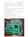
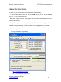
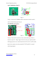
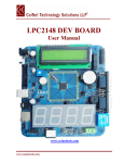
Innovate Engineering solution
LPC2148 Development Board
LPC2148 DEVELOPMENT BOARD
USER MANUAL JULY 2011
Innovate Engineering solution
www.iesolution.in
1
Innovate Engineering solution
LPC2148 Development Board
1. INTRODUCTION:
1.1 Board Features
LPC2148 Development Board is a powerful development platform based on
LPC2148 ARM7TDMI microcontroller with 512K on-chip memory. This board is ideal
for developing embedded applications involving high speed wireless communication,
USB based data logging, real time data monitoring and control, interactive control panels
etc. The on-chip USB controller provides direct high speed interface to a PC/laptop with
speeds up to 12Mb/s. The UART boot loader eliminates need of an additional
programmer and allows you to program using serial port The on board peripherals
include SD/MMC card interface, USB2.0 interface, can be load any I2C 8 Pin EEPROM,
Xigbee wireless module interface, two Bidirectional buffer I/O, ULN2003 500mA
current sinking driver, L293D DC motor controller, 16X2 character LCD, TFT LCD and
many more. The on-chip peripherals and the external hardware on the development board
are interconnected using pin headers and jumpers. The I/O pins on the microcontroller
can be accessed from a 50 pin male header. The board is made from double sided PTH
PCB board to provide extra strength to the connector joints for increased reliability. It
supports the operating supply voltage between 9V to 12V
Innovate Engineering solution
www.iesolution.in
2
Innovate Engineering solution
LPC2148 Development Board
1.1 SPECIFIACTION
•
Microcontroller: LPC2148 with 512K on chip memory
•
Crystal for LPC2148: 12Mhz, Crystal for RTC: 32.768KHz with backup battery
•
50 pin Berg header for external interfacing
•
Operating Supply: 9V to 12V DC/AC
•
2.4GHz Xigbee wireless module adaptor
•
I2C external EEPROM AT24C16
•
USB Type B Connector
•
SD / MMC card holder
•
Direct JTAG connection through PC parallel pot for flashing and debugging
program
•
50 Pin Expansion header
•
TFT LCD 132 X 132 Pixel
•
L293D 600mA Dual DC motor Driver
•
ULN2003 500mA Driver
•
Dual RS232 UART for external communication
•
Real time clock with battery holder
•
2 analog potentiometer connected to ADC
•
4 user switches
•
4 user LED’s
•
Rest and boot loader switch
•
ON/OFF switch
•
Buzzer
Innovate Engineering solution
www.iesolution.in
3
Innovate Engineering solution
•
LPC2148 Development Board
Schematic and application examples in KEIL provided in the document CD
Kit Contains:
1-LPC2148 Pro Development Board
1-Documentation CD
Note: Xigbee wireless module and SD/MMC card are not included with the board and it
can be bought separately from www.iesoulution.in
1.2 LPC2148 Features:
• 16-bit/32-bit ARM7TDMI-S microcontroller in a tiny LQFP64 package.
• 40 kB of on-chip static RAM and 512 kB of on-chip flash memory.
• In-System Programming/In-Application Programming (ISP/IAP) via on-chip boot
loader software.
• Embedded ICE RT and Embedded Trace interfaces offer real-time debugging with the
on-chip Real
Monitor software and high-speed tracing of instruction execution.
• USB 2.0 Full-speed compliant device controller with 2 kB of endpoint RAM.
• Two 10-bit ADCs provide a total of 14 analog inputs
• Single 10-bit DAC provides variable analog output
• Two 32-bit timers/external event counters (with four capture and four compare channels
each), PWM unit (six outputs) and watchdog.
• Low power Real-Time Clock (RTC) with independent power and 32 kHz clock input.
• Multiple serial interfaces including two UARTs, two Fast I²C-bus (400 kbit/s), SPI and
SSP with buffering and variable data length capabilities.
Innovate Engineering solution
www.iesolution.in
4
Innovate Engineering solution
LPC2148 Development Board
• Vectored Interrupt Controller (VIC) with configurable priorities and vector addresses.
• Up to 45 of 5 V tolerant fast general purpose I/O pins in a tiny LQFP64 package.
• 60 MHz maximum CPU clock available from programmable on-chip PLL with settling
time of 100 us.
• On-chip integrated oscillator operates with an external crystal from 1 MHz to 25 MHz
• Power saving modes include Idle and Power-down.
• Individual enable/disable of peripheral functions as well as peripheral clock scaling for
additional power optimization.
• Processor wake-up from Power-down mode via external interrupt or BOD.
• Single power supply chip with POR and BOD circuit
• CPU operating voltage range of 3.0 V to 3.6 V (3.3 V +- 10 pct) with 5 V tolerant I/O
pads.
4
6
7
8
2
26
5
9
23
24
14
3
1
10
22
17
21
16
18
12
20
Innovate Engineering solution
www.iesolution.in
13
15
19
11
25
5
Innovate Engineering solution
LPC2148 Development Board
LPC2148 DEVELOPMENT BOARD OVERVIEW
1. LPC2148 plug in module
2. UART 0 ( controller auto programming : Note : use all pins from the PC)
3. UART 1 ( Switch Option to Xigbee )
4. JTAG & PORT jumper selection
5. JTAG Programmer
6. BOOT & RESET switch ( Main use for JTAG programmer )
7. Power supply
8. 5V output for external hardware interface
9. 3.3 output for external hardware interface
10. Buzzer
11. 4 LED’s
12. 2 X 16 LCD display
13. 4 Interrupt Switch
14. ADC Reference adjust
15. ADC Potentiometer
16. I2C EEPROM AT24C32
17. L293D DC motor driver
18. Jumper selection Port directional control buffer ( P0.19 to P0.7 )
19. Jumper selection Port directional; control buffer ( P1.16 to P1.23 )
20. ULN2003 Relay driver ( can use for stepper motor driver )
21. All I/O output put header
22. Xigbee interface socket
Innovate Engineering solution
www.iesolution.in
6
Innovate Engineering solution
LPC2148 Development Board
23. TFT LCD Display 132 X132 pixel
24. USB interface
25. SPI – SD/MMC interface
26. 3.3V battery back for RTC
2. UART 0
(Controller auto programming: Note: use all pins from the pc serial
port)
2
2
J1 J2 J3 J4 J5 J6 J7
Fig: 1
LPC2148 microcontroller incorporates a capability to self program itself using the onchip UART boot loader. This eliminates the need of an external programming hardware.
The boot loader code is dedicated to use UART0 on the microcontroller. Once the code is
loaded on the microcontroller UART0 is free to be used in the application. The host, in
this case PC or Laptop, requires software to transmit the hex file to the microcontroller
over the serial link. For demonstration purpose we will use Flash Magic programming or
Philips (LPC 2000 flash utility).
Innovate Engineering solution
www.iesolution.in
7
Innovate Engineering solution
LPC2148 Development Board
OPERATING PROCEDURE:
To enter in to the boot load mode follow the below mentioned steps:
1. Connect a DB9 cable between the selected COMx port on your PC and the UART0
port on LPC2148 development board.
2. Plug in an AC/DC 9V or 12V /1A supply to the development board and slide ON/OFF
switch to ON position
3. Jumper Settings – Close the Jumper J1, J2, J3, J5 & J6 as shown in Fig: 1, for both
Serial & JTAG programming, if required as port one the jump and use it as Port Pins
4. Programming Methods:
4.1Using flash Magic Programming:
3.1 Using Philips (LPC 2000 flash utility) Programming:
http://www.flashmagictool.com/
http://www.esacademy.com/fag/docs
Innovate Engineering solution
www.iesolution.in
8
Innovate Engineering solution
LPC2148 Development Board
4.1.1 In the Options — Advanced Options dialog, select the Hardware Config tab, then
check the Use DTR and RTS to control RST and P0.14 check box.
Using the above option the hardware will set to stand alone programming, No need of
using the Step 4.2
4.2 Manual method for Flash magic programming
Enter in to boot load mode by keeping the BOOT switch pressed and then
press RESET switch. Release BOOT switch after reset, then press the start button to
flash magic to start programming
4.3 Using Philips (LPC 2000 flash utility):
Check the user manual in CD to learn the operation
Innovate Engineering solution
www.iesolution.in
9
Innovate Engineering solution
LPC2148 Development Board
3) UART 1 (Switch Option to Xigbee)
3
Fig 2
Using jumper setting selected the UART 1 and Xigbee, as shown in fig 2; with
option we can use the UART 1 for external hardware connection like GSM, GPS and
other sensors.
Innovate Engineering solution
www.iesolution.in
10
Innovate Engineering solution
LPC2148 Development Board
4) JTAG & PORT jumper selection
5) JTAG PROGRAMMING
6
5
2
4
J1 J2 J3 J4 J5 J6 J7
Fig 3
2.1 Use jumper setting to select the JTAG programming,
2.2 This programming option allow user to save the programming time ( for large
memory programming) compare to flash magic and other tools.
2.3 This also allow the user to debug the programming through Keil software, but
this option is not tried till now, in next user manual
2.4 To use the JTAG programming, need parallel port in PC and other programming
software will available in CD.
2.5 JTAG programming Method using H JATG software
http://www.hjtag.com/product_intro.html
Check the user manual and required software given in the CD, follow the
use manual procedure to program the LCP2148, 100% working and tested.
Innovate Engineering solution
www.iesolution.in
11
Innovate Engineering solution
LPC2148 Development Board
6) BOOT & RESET switch (Main use for JTAG programmer)
Enter in to boot load mode by keeping the BOOT switch pressed and then
press RESET switch. Release BOOT switch after reset, then press the start button to
flash magic to start programming
7) Power supply 8) 5V output for external hardware interface
9) Output for external hardware interface
8
7
9
Fig: 4
The power supply is design with Dual voltage regulator with LM317, which supply
3.3VDC and 5VDC with 1A current delivery capacity as shown in fig: 7 and extra power
supply output is given, Identification 8 & 9 gives the power supply 5V & 3.3V
respectively, Use DC 12V or 9V DC adapter and switch on the board using ON/OFF
switch.
CAUTION:
While using the this power supply with external hardware, be sure that the current
should not exceeds above 1A, if exceeds, the development board function will get
affected and any short circuit are maul function by the external or internal hardware using
power supply , the product developer are supplier will not be responsible
Innovate Engineering solution
www.iesolution.in
12
Innovate Engineering solution
LPC2148 Development Board
10. Buzzer
10
Fig: 5
The fig: 5 show the buzzer option, using the jumper selection option, we can isolate the
buzzer and port pins P0.30, the buzzer is operated with 5V Dc supply and it switch using
BC557 with low logic.
11. 4 LED’s
11
Fig: 6
The Fig: 6 shows the 4 LED, which is connected through to a bidirectional buffer in port
P1.16 to P1.19, to use this LED’s connect the buffer input jumps and output LED jumps
and to select the output direction selected the jump as show in figure, for more
information read the 74HC245 Datasheet.
Innovate Engineering solution
www.iesolution.in
13
Innovate Engineering solution
LPC2148 Development Board
12. 2 X 16 LCD Display
12
Fig: 7
The fig: 7 show the 2 X16 LCD display, which is operated in 8 bit mode from the P0.15
to P0.22 (D0 to D7), and RS- P0.25, E/W – P0.28 & E – P0.29 connected to jump and
VR2 POT is provided to adjust the display contrast and below the LCD Jump is provided
to control the LCD Backlight
13. 4 Interrupt Switch
13
Fig: 8
The fig: 8 shows the 4 interrupt switches connected to SW1 - P1.25/E1NTo, SW2 –
P0.14, SW3 – P0.7/E1NT2, SW4 – P0. Using the jump selection the Port and switch can
be isolated
Innovate Engineering solution
www.iesolution.in
14
Innovate Engineering solution
LPC2148 Development Board
14. ADC Reference Adjust
14
Fig: 9
The Fig : 9 Show the ADC reference adjustment, 2K POT is diffuse to adjust the
ADC Reference.
15. ADC Potentiometer
15
Fig: 10
The fig: 10 shows the ADC potentiometer, which is connected in P0.6/AD1.0 and
P0.5/AD0.7 with jump isolating the port and POT, by adjusting the reference pot in fig: 9
the ADC reference voltage will changed, you can check the function in DEMO program.
Innovate Engineering solution
www.iesolution.in
15
Innovate Engineering solution
LPC2148 Development Board
16. I2C EEPROM AT24C32
15
Fig: 11
The fig: 11 shows the I2C EEPROM, which is connected to a Port P0.2 and P0.3,
which is isolated with jump pin from port.
17. L293D DC motor driver
17
DC Supply
Motor 1 & 2
Fig: 12
The Fig: 12 show the DC motor driver section, which s build using L239D, it’s
function is equal to H – bridge, Supply to the motor can be give separately and the
following port pins are use to control motor direction P1.16 to P1.16 and The enable
pins also have option to select from controller P0.7.ENT2 and P0.21 or manual
enable using jump pins
Innovate Engineering solution
www.iesolution.in
16
Innovate Engineering solution
LPC2148 Development Board
18. Jumper selection Port directional control buffer ( P0.19 to P0.7 )
19. Jumper selection Port directional; control buffer ( P1.16 to P1.23
)
19
18
Fig: 13
Fig: 14
The fig: 13 & 14 shows the bidirectional buffer, fig: 13 which is connected from P0.0 to
P0.7, isolated with jump and fig 14 which is connected P1.16 to P1.23, both the buffer
can be operated as input or output pout by selecting the jumper, this kind of option is
given for interface the external hardware like sensors which operates at 5V, by reading
the 78LS245. You can get a clear idea to use this option.
Innovate Engineering solution
www.iesolution.in
17
Innovate Engineering solution
LPC2148 Development Board
20. ULN2003 Relay driver ( Can use for stepper motor driver )
20
Fig: 15
This fig: 15 show the ULN2003APG/AFWG Series are high voltage, high current
Darlington drivers comprised of seven NPN Darlington pairs, which can use to drive the
Relay, stepper motor; power transistor like TIP 122 etc. six inputs are connected with
P1.20 to P1.25 ports and isolated with jumps and a 5Vcc, GND option is added with 8 pin
RMC for easy external hardware operation.
21. All I/O output put header
21
Fig: 16
The fig: 16 show the 26 pin header which has the output of all port pins with addition
with 3.3Vcc and GND as shown in figure.
Innovate Engineering solution
www.iesolution.in
18
Innovate Engineering solution
LPC2148 Development Board
22. Xigbee interface socket
22
Fig: 17
The Fig: 17 shows the Xigbee socket which is contend with UART 1 by selecting the
jumps given aside, All Xigbee pins are take out as single row header pins for external
use.
23. TFT LCD Display 132 X132 pixel
23
Fig: 18
The fig : 18 shows the TFT LCD Display of 132 X 132 pixel , which is used in the
NOKIA mobile phones, by selecting the jumps pins display can be active and the Demo
hex code is give to operate the TFT display with additional software and IC datasheet are
given to develop the Code.
Innovate Engineering solution
www.iesolution.in
19
Innovate Engineering solution
LPC2148 Development Board
24. USB interface
24
Fig: 19
The fig: 19 show the USB Connector which use for connecting the external USB
hardware and PC to share data, this code is not included with development board, which
will be given very Soon for the user, so keep track on the www.iesolution.in
25.SPI – SD/MMC interface
25
Fig: 20
The Fig: 20 shows the SD memory card interface, which is operated in SPI
communication to store the data and use as external read / write memory and it is
connected in P0.5 to P0.7 with jump selection.
26. 3V battery backup for RTC
26
Fig: 21
The fig :21 shows the RTC backup of 3.3V, which is used to HOLD the RTC function
even the power fails, since the battery is inserted in the Board, so the controller will be in
the power up condition even the external power is disconnected.
Innovate Engineering solution
www.iesolution.in
20