1
SPACE 3D CAPACITANCE EXTRACTION
USER’S MANUAL
A.J. van Genderen, N.P. van der Meijs
Department of Electrical Engineering
Delft University of Technology
The Netherlands
Report ET-NT 94.37
Copyright 1994, 1995 by the authors.
All rights reserved.
Last revision:
September, 1995.
Space 3D Capacitance Extraction
1
1. Introduction
1.1 3D Capacitance Extraction
Parasitic capacitances of interconnects in integrated circuits become more important as
the feature sizes on the circuits are decreased and the area of the circuit is unchanged or
increased. For submicron integrated circuits - where the vertical dimensions of the wires
are in the same order of magnitude as their minimum horizontal dimensions - 3D
numerical techniques are even required to accurately compute the values of the
interconnect capacitances.
This document describes the layout-to-circuit extraction program space, that is used to
accurately and efficiently compute 3D interconnect capacitances of integrated circuits
based upon their mask layout description. The 3D capacitances are part of an output
circuit together with other circuit components like transistors and resistances. This
circuit can directly be used as input for a circuit simulator like SPICE.
1.2 Space Characteristics
To compute 3D interconnect capacitances, space uses a boundary-element method. In the
boundary-element method, elements are placed on the boundaries of the interconnects.
This has as an advantage over the finite-element and the finite-difference method (where
the domain between the conductors is discretized) that - especially for 3D situations - a
lower number of discretization elements is used. However, a disadvantage of the
boundary-element method is that in order to compute the capacitance matrix it requires
the inversion of a full matrix of size N×N, where N is the total number of elements. This
takes O (N 3 ) time and O(N 2 ) memory.
To reduce the complexity of the above problem, space employs a new matrix inversion
technique that computes only an approximate inverse. In practice, this means that only
coupling effects are computed between ‘‘nearby’’ elements and that no coupling
capacitances are found between elements that are far apart. For flat layout descriptions,
this method has a computation complexity that is O (N) and a space complexity that is
O (1). As a result, space is capable of quickly extracting relatively large circuits (> 100
transistors), and memory limitations of the computer are seldom an insurmountable
obstacle in using the program.
1.3 Documentation
Throughout this document it is assumed that the reader is familiar with the usage of
space as a basic layout-to-circuit extractor, i.e. extraction of transistors and connectivity.
This document only describes the additional information that is necessary to use space
The Nelsis IC Design System
Space 3D Capacitance Extraction
2
for 3D capacitance extraction. The usage of space as a basic layout-to-circuit extractor is
described in the following documents:
a
space user’s manual
This document describes all features of space except for the 3D capacitance
extraction mode. It is not an introduction to space for novice users, those are
referred to the space tutorial.
a
space tutorial
The space tutorial provides a hands-on introduction to using space and the
auxiliary tools in the system that are used in conjunction with space. It contains
several examples.
a
manual pages
For space as well as for other tools that are used in conjunction with space, manual
pages are available describing (the usage of) these programs. The manual pages
are on-line available, as well as in printed form. The on-line information can be
obtained using the icdman program.
1.4 On-line Examples
Two examples are presented in this manual that are also available on-line. We will
assume that the space software has been installed under the directory ˜cacd. The
examples are then found in the directories ˜cacd/demo/poly_5_10 and
˜cacd/demo/sram_cmos respectively.
NOTE:
The current version of space can only compute 3D capacitances for orthogonal
layouts.
The Nelsis IC Design System
Space 3D Capacitance Extraction
3
2. Program Usage
2.1 General
3D capacitance extraction can be performed using one of the following versions of
space: space3d (for batch mode extraction) and Xspace (for interactive extraction,
including mesh visualization).
When enabling the 3D capacitance extraction mode of space, the program will always
perform a flat extraction.
2.2 Batch Mode Extraction
In order to use the 3D capacitance extraction mode of space3d, use the option -3. Also,
use either the option -c or the option -C. In both cases, 3D ground and coupling
capacitances are computed. However, only in the second case all these capacitances will
be part of the output circuit. In the first case, all coupling capacitances will be
reconnected to ground.
2.3 Interactive Extraction
For 3D capacitance extraction it may be helpful to use a special version of space that is
called Xspace. This version runs under X-windows and uses a graphical window to,
among other things, show the 3D mesh that is generated by the program. Interactively,
the user can select the cell that is extracted, the options that are used, and the items that
are displayed.
For 3D capacitance extraction using Xspace, turn on "3D capacitance" and either
"coupling cap" or "capacitance" in the menu "options". To display also the 3D mesh,
click on "DrawSpider" and "3 dimensional" (and possibly "DrawGreen") in the menu
"display". Then, after selecting the name of the cell in the menu "database", the
extraction can be started by clicking on "extract" in the menu "Extract".
To preview the mesh for 3D capacitance computation, use Xspace as described above
and turn on "3D mesh only" instead of "3D capacitance".
The Nelsis IC Design System
Space 3D Capacitance Extraction
4
3. Technology Description
3.1 Introduction
For 3D extraction, the space element definition file is extended with a description of the
vertical dimensions of the conductors. Information about this extension is given in the
following section. For basic information about the development of an element definition
file, see the Space User’s Manual.
3.2 Extensions for 3D Extraction
For 3D extraction extraction, a vertical dimension list should be included at the end of
the element definition file. Optionally the unit for distances in the vertical dimension list
is specified in the unit specification of the element definition file.
3.2.1 Unit specification
A unit for the vertical dimension list is specified by means of the keywords unit and
vdimension, followed by the value of the unit.
Example:
The following specifies a unit of 1 micron for the distances that are given in the
vertical dimension list:
unit vdimension
1e-6
# Micron
3.2.2 The vertical dimension list
Syntax:
vdimensions :
name : condition_list(s) : mask : bottom thickness
.
.
The vertical dimension list specifies for different conductors under different conditions
(e.g. metal2 above polysilicon or metal2 above metal1) (1) bottom: the distance between
the substrate and the bottom of the conductor (2) thickness: the thickness of the
conductor
Example:
An example of an almost minimal technology file (with corresponding geometry)
is given below. While minimal, this file can actually be complete for 3D extraction
for a double metal process in which only metal1 and metal2 capacitances are
extracted.
The Nelsis IC Design System
Space 3D Capacitance Extraction
unit vdimension
1e-6
5
# meter
conductors :
metal1 : in : in : 0
metal2 : ins : ins : 0
vdimensions :
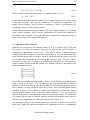
metal1_shape : in : in : 1.6 1.0
metal2_shape : ins : ins : 3.3 1.2
ins
1.0µ
1.2µ
in
3.3µ
1.6µ
At a transition area, where a conductor goes from one bottom and thickness specification
to another bottom and thickness specification, the slope of the conductor is determined by
the parameter default_step_slope (see Section 4.3).
NOTE:
To prevent the overlap of different transition areas of one conductor (which
currently results incorrect element meshes), the differences in bottom and
thickness specifications of one conductor may not be too large (otherwise: increase
the parameter default_step_slope).
3.2.3 The edge shape list
Syntax:
eshapes :
name : condition_list(s) : mask : dxb dxt
.
.
The edge shape list specifies for different conductors, the extension of each conductor in
the x direction relative to the position of the original conductor edge in the layout. The
first value (dxb) specifies the extension of the bottom of the conductor and the second
value (dxt) specifies the extension of the top of the conductor.
The Nelsis IC Design System
Space 3D Capacitance Extraction
6
Example:
eshapes :
metal1_eshape : in
: in
: 0.2 0.1
0.1µ
in
0.2µ
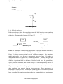
3.2.4 Diffused conductors
Diffused conductors (which for example implement the MOS transistor source and drain
regions) are described in a somewhat different way than the poly-silicon and the metal
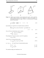
conductors. The approach is illustrated in Figure 3.1.
metal
metal
diff model
diff
locos
ground
field implant
(a)
(b)
Figure 3.1. Illustration of the heuristic approach to incorporate diffusion capacitances,
physical structure (a) and 3D capacitance model (b).
Figure 3.1.a shows a cross-sectional view of a diffused conductor. The capacitance
model employed by space for such a conductor is shown in Figure 3.1.b, where the
diffused interconnect is replaced by a thin sheet conductor. Therefore, the user must
specify in the element definition file a zero thickness for the conductor. The sheet
conductor is positioned half the thickness of the field oxide above the ground plane,
which is flat and continuous, and must be thought of as modeling the top side of the
diffused conductors.
The program computes the coupling capacitances between these sheet conductors and the
other conductors, and mutually between sheet conductors. These capacitances are
inserted in the extracted circuit. For the sheet conductors, the 3D capacitance extraction
method also yields the capacitances to the substrate. These capacitances are however
better represented by junction capacitances that are computed using an area/perimeter
The Nelsis IC Design System
Space 3D Capacitance Extraction
7
method. Therefore, the 3D capacitances between sheet diffused conductors and the
substrate are discarded by the program. The junction capacitances must be specified
separatedly by the user in the element definition file.
Although this approach is purely heuristic, its results are satisfactory when the width of
the diffusion paths is large enough compared to the height of the sheet conductors above
the ground plane.
A conductor is defined as a diffused conductor within space if, in the element definition
file of space, the type of the conductor is specified as ’n’ or ’p’.
3.2.5 Non-3D capacitances
When extracting 3D capacitances, non-3D capacitances that are specified in the element
definition file are not extracted, except for the ground capacitances of diffused
conductors.
The Nelsis IC Design System
Space 3D Capacitance Extraction
8
4. 3D Capacitance Computation
4.1 Introduction
Space uses a boundary-element method to compute 3D capacitances (see Appendix A).
Since there are several degrees of freedom with this method, there are also several
parameters that can be set with space during 3D capacitance extraction. A brief
description of these parameters is given below. For more background information on the
parameters, the reader is referred to Appendix A.
The parameters are set in the space parameter file (see also the Space User’s Manual).
All lengths and distances are specified in micron and all areas are specified in square
micron.
4.2 Dielectric
dielectric1 name permittivity bottom
dielectric2 name permittivity bottom
dielectric3 name permittivity bottom
Specifies the dielectric structure of the chip. Up to 3 dielectric layers can be specified.
For each layer, name is an arbitrary label that will be used for error messages etc,
permittivity is a real number giving the relative dielectric constant, and bottom specifies
(in microns) the bottom of the dielectric layer. Dielectric1 must specify the lowest
dielectric, dielectric2 the second lowest, etc. For dielectric1 bottom must be zero. The
top of a dielectric layers is at the bottom of the next dielectric. The top of the last
dielectric is at infinity. No dielectric layer means vacuum. If one or more dielectric
layers are specified, a ground plane at zero is present.
4.3 Mesh Construction
default_step_slope slope
(default: 0.5)
Specifies the tangent of the slope of conductors at steps in height above the substrate (e.g.
the transition of metal above polysilicon to metal not above polysilicon).
NOTE:
To prevent the overlap of different transition areas of one conductor (which
currently results incorrect element meshes), the value of default_step_slope may
not be too small.
max_be_area area
This parameter specifies (in square microns) the maximum area of the boundary
The Nelsis IC Design System
Space 3D Capacitance Extraction
9
elements. This parameter has no default and must therefore always be specified when
performing 3D extraction.
be_shape number (default: 1)
Enforces a particular shape of the boundary element faces. Value 1 means no
enforcement. Value 3 means triangular faces. Value 4 means quadrilateral faces (only
valid with constant shape functions; see below).
4.4 Shape and Weight Functions
be_mode mode
(default: 0c)
Specifies the type of shape functions and the type of weight functions that are used (see
Section A.2).
iiiiiiiiiiiiiiiiiiiiiiiiiiiiiiiiiiiiii
mode
shape function
weight method
iiiiiiiiiiiiiiiiiiiiiiiiiiiiiiiiiiiiii
0c
piecewise constant
collocation
1c
piecewise linear
collocation
0g
piecewise constant
Galerkin
1g
piecewise linear
Galerkin
iiiiiiiiiiiiiiiiiiiiiiiiiiiiiiiiiiiiii
An example of a piecewise constant shape functions is given in Figure A.1.b. An
example of a linear shape functions is given in Figure A.1.c. In general, it is
recommended not to use mode 1c due to its poor numerical behavior. Further, given a
certain accuracy, the Galerkin method, as compared to the collocation method, allows to
use larger elements.
collocation_green distance
Perform collocation instead of Galerkin computations for elements more then the
specified distance apart. The default is 0 if be_mode is equal to collocation, 0c or 1c. It
is infinity otherwise
point_green distance
(default: infinity)
Use point charges and perform collocation for elements more then the specified distance
apart.
4.5 Accuracy of Elastance Matrix
green_eps error (default: 0.001)
Positive real value specifying the relative accuracy for evaluating the entries in the
elastance matrix.
The Nelsis IC Design System
Space 3D Capacitance Extraction
10
4.6 Window Size
cap3d_window w
cap3d_window wx wy
Specifies the size (in micron) of the influence window. All influences between elements
that are within a distance w will be taken into account, and all influences between
elements that are more than a distance 2w apart will not be taken into account (see
Section A.3). If only one value is given, this value specifies the size of the window in the
x direction and the y direction. If two values are given, the first value specifies the size
of the window in the x direction and the second value specifies the size of the window in
the y direction.
The extraction time is proportional to O(Nw 4 ), where N is the number of elements. The
memory usage of the program is O(w 4 ). A reasonable value for cap3d_window is 1-3
times the maximum height of the circuit. No default.
4.7 Example Parameter File
An example of parameter settings for 3D capacitance extraction is as follows:
#
#
dielectric1
dielectric2
name
======
SiO2
air
max_be_area
cap3d_window
1.0
5.0
permit.
=======
3.9
1.0
bottom
=========
0.0
3.0
4.8 Run-time Versus Accuracy
The runtime of the program is largely dependent on the values of the parameters that are
used. For example, if max_be_area is decreased (smaller elements are used), the
accuracy will increase but also the number of elements will increase and the computation
time will become larger. The larger the size of the window, the more accurate results are
obtained but also longer extraction times will occur. The Galerkin method is more
accurate than the collocation method, but it also requires more computation time.
Also, 3D capacitance computation for configurations consisting of 2 or 3 dielectric layers
may require much more computation time than the same computation for configurations
consisting of 1 dielectric layer. This is because the computation of the Green’s functions
requires much more time. In this case, the computation time can be decreased (on the
penalty of some loss in accuracy) by increasing the value for the maximum error for the
evaluation of the entries in the elastance matrix (green_eps).
The Nelsis IC Design System
Space 3D Capacitance Extraction
11
5. Examples
5.1 5 Parallel Conductors
As a first example we show how space is used to compute 3D capacitances for a
configuration consisting of 5 parallel conductors. To run the example, first create a
project, e.g. with name "exam1", for an scmos_n process and with lambda is 0.1
% mkpr exam1
available processes:
process id
process name
3
scmos_n
23
dimes01
select process id (1 - 23): 3
enter lambda in microns (>= 0.001): 0.1
Next, go to the project directory and copy the example source files from the directory
˜cacd/demo/poly_5_10 (it is supposed that demo directory has been installed under
˜cacd).
% cd exam1
% cp ˜cacd/demo/poly_5_10/* .
The layout description is put into the database using the program cgi.
% cgi poly_5_10.gds
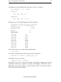
The layout of the configuration is shown below (e.g. use Xdali to inspect the layout). The
conductors have a length of 10 micron, a width of 1 micron, a height of 1 micron and
their separation is also 1 micron.
a
b
c
d
The Nelsis IC Design System
e
Space 3D Capacitance Extraction
12
An appropriate element definition file (with name "tech.s") is as follows:
unit vdimension
1e-6
# meter
conductors :
resP : cpg : cpg : 0.0
vdimensions :
dimP : cpg : cpg : 1.0 1.0
Furthermore, we use the following parameter file ("param.p"):
# Dielectric consists of 5 micron thick SiO2
# (epsilon = 3.9) on a conducting plane.
dielectric1 SiO2
3.9 0.0
dielectric2 air
1.0 5.0
be_mode
max_be_area
cap3d_window
0c
2
2
color_cpg
color_caa
color_cmf
color_cms
color_cca
color_ccp
color_cva
color_cwn
color_csn
color_cog
color_cx
red
green
blue
gold
black
black
black
glass
glass
glass
glass
Then, after having run tecc on the element definition file,
% tecc tech.s
we extract a circuit description for the layout of the cell as follows:
% space3d -C3 -E tech.t -P param.p poly_5_10
Alternatively Xspace can be used.
% Xspace -E tech.t -P param.p
Click button "poly_5_10" in the menu "database", click button "coupling cap" and "3D
capacitance" in the menu "options", click button "DrawSpider", "DrawGreen" and "3
dimensional" in the menu "display", and click button "extract" in the menu "Extract".
This will yield the following picture:
The Nelsis IC Design System
Space 3D Capacitance Extraction
13
The circuit that has been extracted can be inspected using the program xspice
% xspice -a poly_5_10
poly_5_10
* circuit poly_5_10 nbulk e d c b a
c1 a c 19.58371e-18
c2 a b 508.8933e-18
c3 a GND 1.211898f
c4 b d 18.84548e-18
c5 b c 502.5777e-18
c6 b GND 885.7932e-18
c7 e c 18.84548e-18
c8 e d 510.213e-18
c9 e GND 1.211244f
c10 c d 502.5814e-18
c11 c GND 872.8481e-18
c12 d GND 884.4351e-18
* end poly_5_10
Note that there are no capacitances between conductors that are more than a distance 2 *
cap3d_window apart (e.g. conductor a and conductor d or conductor a and conductor e).
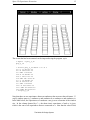
In the table below, the capacitances of conductor a are given as a function of the window
size. In the column denoted by Cs a , the short-circuit capacitance of node a is given,
which is the sum of all capacitances that are connected to a. Note that the value of this
The Nelsis IC Design System
Space 3D Capacitance Extraction
capacitance is almost independent on the size of the window.
i iiiiiiiiiiiiiiiiiiiiiiiiiiiiiiiiiiiiiiiiii
w
capacitances (10−18 F)
(µ)
Ca gnd
Ca b
Ca c
Ca d
Ca e
Cs a
i iiiiiiiiiiiiiiiiiiiiiiiiiiiiiiiiiiiiiiiiii
2 1211.9 508.9 19.58
1740.4
4 1166.3 521.8 36.12 13.94 3.68 1741.8
6 1157.0 523.4 36.83 13.73 7.00 1738.0
8 1153.0 524.3 37.35 14.01 7.20 1735.9
1152.4 524.4 37.43 14.06 7.24 1735.5
i10
iiiiiiiiiiiiiiiiiiiiiiiiiiiiiiiiiiiiiiiiii
The Nelsis IC Design System
14
Space 3D Capacitance Extraction
15
5.2 Cmos Static RAM Cell
The next example consists of a cmos static RAM cell in 1.0µ technology. To run the
example, first create a project, e.g. with name "exam2", for an scmos_n process and with
lambda is 0.5
% mkpr exam2
available processes:
process id
process name
3
scmos_n
23
dimes01
select process id (1 - 23): 3
enter lambda in microns (>= 0.001): 0.5
Next, go to the project directory and copy the example source files from the directory
˜cacd/demo/sram.
% cd exam2
% cp ˜cacd/demo/sram/* .
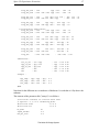
The layout of the ram cell is put into the database as follows
% cgi sram.gds
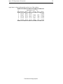
A picture of the layout is shown below.
t_vss
bit
c1
vdd
word
c2
notbit
b_vss
The following technology file ("sram.s") is used for extraction:
The Nelsis IC Design System
Space 3D Capacitance Extraction
#
#
#
#
#
#
#
#
#
#
16
space element definition file for scmos_n example process
masks:
cpg - polysilicon interconnect
caa - active area
cmf - metal interconnect
cms - metal2 interconnect
cca - contact metal to diffusion
ccp
cva
cwn
csn
cog
-
contact metal to poly
contact metal to metal2
n-well
n-channel implant
contact to bondpads
See also: maskdata
maxkeys 13
unit
unit
unit
unit
unit
unit
unit
resistance
c_resistance
a_capacitance
e_capacitance
capacitance
vdimension
shape
conductors :
# name
:
cond_mf :
cond_ms :
cond_pg :
cond_pa :
cond_na :
1
1e-12
1e-6
1e-12
1e-15
1e-6
1e-6
#
#
#
#
#
#
#
Ohm
Ohm per micro-meterˆ2
Farad per meterˆ2
Farad per meter
Farad
meter
meter
condition
cmf
cms
cpg
caa !cpg !csn
caa !cpg csn
:
:
:
:
:
:
mask
cmf
cms
cpg
caa
caa
:
:
:
:
:
:
fets :
# name : condition
: gate d/s
nenh : cpg caa csn : cpg caa
penh : cpg caa !csn : cpg caa
contacts :
# name
cont_s
cont_p
cont_a
:
:
:
:
condition
cva cms cmf
ccp cmf cpg
cca cmf caa !cpg
:
:
:
:
lay1
cms
cmf
cmf
resistivity
0.045
0.030
40
70
50
:
:
:
:
:
:
type
m
m
m
p
n
#
#
#
#
#
first metal
second metal
poly interconnect
p+ active area
n+ active area
# nenh MOS
# penh MOS
lay2
cmf
cpg
caa
: resistivity
:
1
# metal to metal2
: 100
# metal to poly
: 100
# metal to active area
capacitances :
# active area capacitances
# name
: condition
: mask
acap_na : caa !cpg
csn
: caa
ecap_na : !caa !-cpg -csn -caa : -caa
acap_pa : caa !cpg !csn
: caa
ecap_pa : !caa !-cpg !-csn -caa : -caa
:
:
:
:
:
capacitivity
200
# n+ bottom
300
# n+ sidewall
400
# p+ bottom
600
# p+ sidewall
# polysilicon capacitances
acap_cpg_sub : cpg
!caa : cpg : 49
ecap_cpg_sub : !cpg -cpg !cmf !cms !caa : -cpg : 52
# first metal capacitances
The Nelsis IC Design System
# bot to sub
# edge to sub
Space 3D Capacitance Extraction
17
acap_cmf_sub : cmf
!cpg !caa : cmf : 25
ecap_cmf_sub : !cmf -cmf !cms !cpg !caa : -cmf : 52
acap_cmf_caa : cmf
caa !cpg !cca !cca : cmf
ecap_cmf_caa : !cmf -cmf caa !cms !cpg
: -cmf
acap_cmf_cpg : cmf
cpg !ccp : cmf
ecap_cmf_cpg : !cmf -cmf cpg !cms : -cmf
caa : 49
caa : 59
cpg : 49
cpg : 59
# second metal capacitances
acap_cms_sub : cms
!cmf !cpg !caa : cms : 16
ecap_cms_sub : !cms -cms !cmf !cpg !caa : -cms : 51
acap_cms_caa : cms
caa !cmf !cpg : cms caa : 25
ecap_cms_caa : !cms -cms caa !cmf !cpg : -cms caa : 54
acap_cms_cpg : cms
cpg !cmf : cms cpg : 25
ecap_cms_cpg : !cms -cms cpg !cmf : -cms cpg : 54
acap_cms_cmf : cms
cmf !cva : cms cmf : 49
ecap_cms_cmf : !cms -cms cmf
: -cms cmf : 61
lcap_cms
: !cms -cms =cms
: -cms =cms : 0.07
vdimensions :
caa_on_all
cpg_of_caa
cpg_on_caa
cmf
cms
:
:
:
:
:
caa !cpg
cpg !caa
cpg caa
cmf
cms
:
:
:
:
:
caa
cpg
cpg
cmf
cms
:
:
:
:
:
0.30
0.60
0.35
1.70
2.90
0.00
0.50
0.50
0.80
1.00
eshapes :
cpg_edge : cpg !-cpg : cpg : 0 0
cmf_edge : cmf !-cmf : cmf : 0 0
cms_edge : cms !-cms : cms : 0 0
#EOF
Note that for the diffusion area a conductor of thickness 0 is used that is 0.30µ above the
substrate.
The contents of the parameter file ("sram.p") is as follows:
# Dielectric consists of 5 micron thick SiO2
# (epsilon = 3.9) on a conducting plane.
dielectric1 SiO2
3.9 0.0
dielectric2 air
1.0 5.0
be_mode
cap3d_window
max_be_area
0c
4.0
4.0
The Nelsis IC Design System
Space 3D Capacitance Extraction
color_cpg
color_caa
color_cmf
color_cms
color_cca
color_ccp
color_cva
color_cwn
color_csn
color_cog
color_cx
18
red
green
blue
gold
black
black
black
glass
glass
glass
glass
After running tecc on the element definition file,
% tecc sram.s
extraction in batch mode is done by using space3d.
% space3d -C3 -E sram.t -P sram.p sram
For interactive extraction, Xspace is used.
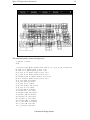
% Xspace -E sram.t -P sram.p
Click button "sram" in the menu "database", click button "coupling cap" and "3D
capacitance" in the menu "options", click button "DrawSpider", "DrawGreen" and "3
dimensional" in the menu "display", and click button "extract" in the menu "Extract".
This will yield the following picture:
The Nelsis IC Design System
Space 3D Capacitance Extraction
The extraction result is retrieved using xspice:
% xspice -a sram
sram
* circuit sram pbulk nbulk word vdd c2 c1 t_vss b_vss notbit bit
m1 vdd c1 c2 pbulk penh_0 w=1u l=1u
m2 vdd c2 c1 pbulk penh_0 w=1u l=1u
m3 b_vss c1 c2 nbulk nenh_0 w=1u l=1u
m4 t_vss c2 c1 nbulk nenh_0 w=1u l=1u
m5 notbit word c2 nbulk nenh_0 w=1u l=1u
m6 bit word c1 nbulk nenh_0 w=1u l=1u
c1 b_vss word 278.0014a
c2 b_vss vdd 198.4933a
c3 b_vss c2 31.93518a
c4 b_vss notbit 889.9239a
c5 b_vss c1 392.6898a
c6 b_vss GND 4.477872f
c7 notbit bit 111.9043a
c8 notbit word 245.2181a
c9 notbit vdd 30.89413a
c10 notbit c2 784.1868a
c11 notbit c1 216.9424a
c12 notbit GND 6.335045f
c13 t_vss word 277.0062a
c14 t_vss vdd 198.334a
c15 t_vss bit 888.854a
The Nelsis IC Design System
19
Space 3D Capacitance Extraction
20
c16 t_vss c2 392.4108a
c17 t_vss c1 32.07229a
c18 t_vss GND 4.478842f
c19 word bit 246.5017a
c20 word c2 167.2504a
c21 word c1 165.8421a
c22 word GND 1.632647f
c23 vdd bit 30.79601a
c24 vdd c2 134.1192a
c25 vdd c1 134.4992a
c26 vdd GND 36.8f
c27 bit c1 783.245a
c28 bit c2 217.3764a
c29 bit GND 6.334444f
c30 c2 c1 1.448497f
c31 c2 GND 13.46282f
c32 c1 GND 13.46465f
* end sram
.model penh_0 pmos(level=2 ld=0 tox=25n nsub=50e15 vto=-1.10 uo=200
+
uexp=100m ucrit=10k delta=200m xj=500n vmax=50k neff=1
+
rsh=0 nfs=0 js=10u cj=500u cjsw=600p mj=500m mjsw=300m
+
pb=800m cgdo=300p cgso=300p)
.model nenh_0 nmos(level=2 ld=0 tox=25n nsub=20e15 vto=700m uo=600
+
uexp=100m ucrit=10k delta=200m xj=500n vmax=50k neff=1
+
rsh=0 nfs=0 js=2u cj=100u cjsw=600p mj=500m mjsw=300m
+
pb=800m cgdo=300p cgso=300p)
vpbulk pbulk 0 5.000000V
rpbulk pbulk 0 100meg
vnbulk nbulk 0 0.000000V
rnbulk nbulk 0 100meg
The Nelsis IC Design System
Space 3D Capacitance Extraction
21
6. Solving Problems
6.1 Long Computation Times
Although space has been implemented with emphasis on efficient 3D capacitance
extraction methods, sometimes, long extraction times may occur. This can happen if too
much time is spend on computations of irrelevant details that do not significantly
increase the accuracy of the extraction results. This for example is the case if the size of
the elements is chosen too small, if the window size is unnecessary large or if linear
shape functions and the Galerkin method are used for too many elements. A good
strategy to circumvent this problem is to first try an extraction with a parameter set that
does not include many details. Next, a parameter set is used in which more details are
included, and the extraction results are evaluated to inspect the influence of the
parameters.
See also Section 4.8.
6.2 Numerical Problems
If the elastance matrix (see Section A.2) is badly conditioned, space may be unable to
invert this matrix and it may give error messages like "domain error(s) in sqrt". One
reason for a badly conditioned elastance matrix is that there is too much difference in
element sizes. A solution in this case is to split the large elements, either by decreasing
the maximum size of the elements or by adding irregularities to the layout using a
symbolic mask. If very thin conductors are used, the difference between the small
vertical elements and the large horizontal elements may also become too large. In this
case, it may for example be better to specify a zero thickness for the conductor in the
element definition file. In general, the creation of small elements that are close to large
elements, and the creation of long and narrow elements, should be avoided.
Also the use of the Galerkin method (mode 0g or 1g) instead of the collocation method
(mode 0c or 1c) might help in the above case. Mode 1g will even be more robust than
mode 0g.
The Nelsis IC Design System
Space 3D Capacitance Extraction
22
Appendix A: 3D Capacitance Model
A.1 Introduction
Space uses a boundary-element method to compute 3D capacitances. A brief description
of this method is given in Section A.2. For the solution of the boundary-element
equations, a large matrix needs to be inverted. The approximate matrix inversion
technique that is used for this is described in Section A.3.
A.2 The Boundary-Element Method
Consider a domain V that contains M conductors. Our purpose is to find the short-circuit
capacitance matrix Cs that gives the relation between the conductor charges
Q T = [Q 1 , Q 2 , . . . QM ] and the conductor potentials ΦT = [Φ1 , Φ2 , . . . ΦM ] as
Q = Cs Φ.
(A.1)
The potential φ(p) at a point p in V can be expressed as [1, 2]
φ(p) = ∫ G(p, q) ρ(q) dq,
(A.2)
V
where ρ(q) is the charge distribution in V and G(p, q) is the Green’s function for V. In
order to solve A.2, the boundary-element method subdivides the surfaces of the
conductors in elements S 1 , S 2 , . . . SN (the elements may partly be overlapping), and
approximates the charge distribution ρ(q) by
N
ρ(q) ∼
∼ ρ̃(q) =
Σ αi fi (q),
(A.3)
i =1
where α1 , α2 , . . . αN are unknown variables to be determined and f 1, f 2 , . . . fN are N
independent shape functions (also called basis functions). The fi ’s have the property that
∫
I
K
L
fi (q) dq =
Sj
1 if i = j
0 if i ≠ j
(A.4)
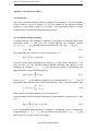
Some examples of shape functions are given in Figure A.1.
An approximation for the potential distribution is then obtained by insertion of A.3 into
A.2:
φ̃(p) =
N
Σ αi S∫ G(p, q) f j (q) dq.
i =1
(A.5)
i
Next, N independent linear equations are obtained by introducing a set of N independent
weight functions w 1 , w 2 , . . . wN that are defined on the sub-areas S 1 , S 2 , . . . SN and
that are used to "average out" the error in φ̃(p):
The Nelsis IC Design System
Space 3D Capacitance Extraction
23
fi (p)
fi (p)
fi (p)
...
. . . . . ....
.S
. ...
... i . . . . . . . . .
.
.
.
...
...
.....
Si
Si
..
...
(a)
(b)
(c)
Figure A.1. Different types of shape or basis functions that can be used to model the
surface charge density on the conductors (a) Dirac, (b) constant: f is
described by the top of the wedge, (c) linear: f is described by the 4 slanting
planes of the pyramid.
R
φ̃(p)
Q
∫ wi (p)
Si
− φ(p) HPdp = 0
(i = 1 . . . N).
(A.6)
By insertion of A.5, the above set of equation may be rewritten as
N
Σ α j S∫ S∫ G(p, q) f j (q) wi (p) dq dp
j =1
i
j
=
∫ wi (p) φ(p)
Si
Now, let F be an N×M incidence matrix in which
I1 if Si is on conductor j
Fij = K
0 otherwise.
L
dp
(i = 1 . . . N).
(A.7)
(A.8)
Then, Equation A.7 may be written as a set of N×N equations,
G α = W F Φ,
(A.9)
where G is an N×N matrix that has entries
Gij =
∫ ∫ G(p,
q) f j (q) wi (p) dq dp,
(A.10)
Si S j
αT = [α1 , α2 , ..., αN ], and W is an N×N matrix that has entries
Wij = 0,
Wii =
i≠j,
(A.11a)
∫ wi (p) dp.
(A.11b)
Si
The conductor charges are found from A.9 as
The Nelsis IC Design System
Space 3D Capacitance Extraction
Q = F T α = F T G −1 W F Φ.
24
(A.12)
Thus, the short-circuit capacitance matrix Cs is obtained from A.12 as
Cs = F T G −1 W F.
(A.13)
In the Galerkin boundary-element method [3] the weight functions wi are chosen equal
to the shape functions. This way, the evaluation of G requires the computation of a
double surface integral, but G becomes symmetrical, which is advantageous for
computing the inverse of the elastance matrix.
In the collocation boundary-element method [4], the weight functions wi are chosen
equal to Dirac functions. In this case the computation of G requires the evaluation of
only single surface integrals. G is artificially made symmetrical by using the average of
the two entries that are at a symmetrical position.
A.3 Approximate Matrix Inversion
Normally, the inversion of the elastance matrix G in A.13 requires O(N 3 ) time and
O(N 2 ) space. To allow fast extraction times, also for large circuits, space is capable of
computing an approximate inverse for G. Therefore, it utilizes a matrix inversion
technique that takes as input a matrix that is specified on a stair-case band around the
main diagonal and produces as output a matrix in which only non-zero entries occur for
the positions that correspond to positions in the stair-case band. The basic idea is
illustrated in Figure A.2. In Figure A.2, different approximations are computed for a
simple boundary-element mesh that consists of 4 elements and that is described by the
following elastance matrix:
R1.0
J
J0.4
J0.2
J0.1
Q
0.4
1.0
0.4
0.2
0.2
0.4
1.0
0.4
0.1 H
J
0.2 J
0.4 J
1.0 J
(A.14)
P
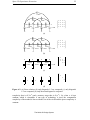
For practical layouts the method proceeds as follows. First, the layout is subdivided into
strips of width w (see Figure A.3). All influences between elements that are within a
distance w will be taken into account, and all influences between elements that are more
than a distance 2w apart will not be taken into account. Next, a banded approximation
according to Figure A.2 is computed - whereby only influences are taken into account
between elements that are in the y direction within a distance w - for (1) each pair of
adjacent strips and (2) each single strip except for the first and last strip. The results that
are obtained for the pairs of strips are added to the total result and the results that are
obtained for the single strips are subtracted from the total result [5, 6, 7].
By executing all steps of the extraction method as a scanline is swept over the layout
from left to right, the extraction method can be implemented to have a computation
The Nelsis IC Design System
Space 3D Capacitance Extraction
25
0.007
0.054
g
g
1
0.454
0.678
0.054
g
2
0.434
0.424
g
3
0.454
0.424
x
x
x
x
4
x
x
x
x
x
x
x
x
x
x
x
x
0.678
(a)
0.059
g
g
0.455
0.681
0.059
g
0.433
0.421
x x x
x x x x
x x x x
x x x
g
0.455
0.421
0.681
(b)
g
g
0.476
0.714
g
0.476
0.429
x x
x x x
x x x
x x
g
0.476
0.429
0.714
(c)
x
g
g
g
x
g
x
x
1
1
1
1
(d)
Figure A.2. (a) Exact solution, (b) only diagonals 1-3 are computed, (c) only diagonals
1-2 are computed, (d) only the main diagonal is computed.
complexity that is O(Nw 4 ) and a memory usage that is O(w 4 ). So, when w is kept
constant, which is reasonable if one type of technology is used, the computation
complexity of the method is linear with the size of the circuit and the space complexity is
constant.
The Nelsis IC Design System
Space 3D Capacitance Extraction
w
Figure A.3. A layout subdivided into strips of width w.
The Nelsis IC Design System
26
Space 3D Capacitance Extraction
27
References
1.
E. Weber, Electromagnetic Fields, Theory and Applications, John Wiley & Sons,
Inc., New York (1957).
2.
P. Dewilde and Z.Q. Ning, Models For Large Integrated Circuits, Kluwer
Academic Publishers (1990).
3.
Z.Q. Ning, P.M. Dewilde, and F.L. Neerhoff, ‘‘Capacitance Coefficients for VLSI
Multilevel Metallization Lines,’’ IEEE Trans. on Electron Devices ED-34(3) pp.
644-649 (March 1987).
4.
Z.Q. Ning and P. Dewilde, ‘‘SPIDER: Capacitance Modelling for VLSI
Interconnections,’’ IEEE Trans. on Computer-Aided Design 7(12) pp. 1221-1228
(December 1988).
5.
N.P. van der Meijs and A.J. van Genderen, ‘‘An Efficient Finite Element Method
for Submicron IC Capacitance Extraction,’’ Proc. 26th Design Automation
Conference, Las Vegas, pp. 678-681 (June 1989).
6.
A.J. van Genderen, ‘‘Reduced Models for the Behavior of VLSI Circuits,’’ Ph.D.
Thesis, Delft University of Technology, Network Theory Section, Delft, the
Netherlands (October 1991).
7.
N.P. van der Meijs, ‘‘Accurate and Efficient Layout Extraction,’’ Ph.D. Thesis,
Delft University of Technology, Network Theory Section, Delft, the Netherlands
(1992).
The Nelsis IC Design System
CONTENTS
1. Introduction
. . . . .
1.1 3D Capacitance Extraction
1.2 Space Characteristics .
1.3 Documentation . . .
1.4 On-line Examples . .
.
.
.
.
.
.
.
.
.
.
.
.
.
.
.
.
.
.
.
.
.
.
.
.
.
.
.
.
.
.
.
.
.
.
.
.
.
.
.
.
.
.
.
.
.
.
.
.
.
.
.
.
.
.
.
.
.
.
.
.
.
.
.
.
.
.
.
.
.
.
.
.
.
.
1
1
1
1
2
2. Program Usage
. . .
2.1 General . . . .
2.2 Batch Mode Extraction
2.3 Interactive Extraction
.
.
.
.
.
.
.
.
.
.
.
.
.
.
.
.
.
.
.
.
.
.
.
.
.
.
.
.
.
.
.
.
.
.
.
.
.
.
.
.
.
.
.
.
.
.
.
.
.
.
.
.
.
.
.
.
.
.
.
.
3
3
3
3
3. Technology Description . . . .
3.1 Introduction . . . . . .
3.2 Extensions for 3D Extraction .
.
.
.
.
.
.
.
.
.
.
.
.
.
.
.
.
.
.
.
.
.
.
.
.
.
.
.
.
.
.
.
.
.
.
.
.
.
.
.
4
4
4
4. 3D Capacitance Computation .
4.1 Introduction . . . . .
4.2 Dielectric . . . . . .
4.3 Mesh Construction . . .
4.4 Shape and Weight Functions
4.5 Accuracy of Elastance Matrix
4.6 Window Size . . . . .
4.7 Example Parameter File
.
4.8 Run-time Versus Accuracy
.
.
.
.
.
.
.
.
.
.
.
.
.
.
.
.
.
.
.
.
.
.
.
.
.
.
.
.
.
.
.
.
.
.
.
.
.
.
.
.
.
.
.
.
.
.
.
.
.
.
.
.
.
.
.
.
.
.
.
.
.
.
.
.
.
.
.
.
.
.
.
.
.
.
.
.
.
.
.
.
.
.
.
.
.
.
.
.
.
.
.
.
.
.
.
.
.
.
.
.
.
.
.
.
.
.
.
.
.
.
.
.
.
.
.
.
.
.
.
.
.
.
.
.
.
.
8
8
8
8
9
9
10
10
10
5. Examples . . . . . .
5.1 5 Parallel Conductors .
5.2 Cmos Static RAM Cell .
.
.
.
.
.
.
.
.
.
.
.
.
.
.
.
.
.
.
.
.
.
.
.
.
.
.
.
.
.
.
.
.
.
.
.
.
.
.
.
.
.
.
.
.
.
11
11
15
6. Solving Problems . . . . .
6.1 Long Computation Times .
6.2 Numerical Problems
. .
.
.
.
.
.
.
.
.
.
.
.
.
.
.
.
.
.
.
.
.
.
.
.
.
.
.
.
.
.
.
.
.
.
.
.
.
.
.
.
.
.
.
21
21
21
Appendix A: 3D Capacitance Model .
A.1 Introduction . . . . . .
A.2 The Boundary-Element Method
A.3 Approximate Matrix Inversion
.
.
.
.
.
.
.
.
.
.
.
.
.
.
.
.
.
.
.
.
.
.
.
.
.
.
.
.
.
.
.
.
.
.
.
.
.
.
.
.
.
.
.
.
.
.
.
.
.
.
.
.
22
22
22
24
References .
.
.
.
.
.
.
.
.
.
.
.
.
.
27
.
.
.
.
.
.
.
.
.
.
.
.
-i-
LIST OF FIGURES
Figure 3.1. Illustration of the heuristic approach to incorporate diffusion
capacitances, physical structure (a) and 3D capacitance model
(b). . . . . . . . . . . . . . . . . . .
.
6
Figure A.1. Different types of shape or basis functions that can be used to model
the surface charge density on the conductors (a) Dirac, (b) constant: f
is described by the top of the wedge, (c) linear: f is described by the 4
slanting planes of the pyramid. . . . . . . . . . . . .
23
Figure A.2. (a) Exact solution, (b) only diagonals 1-3 are computed, (c) only
diagonals 1-2 are computed, (d) only the main diagonal is
computed. . . . . . . . . . . . . . . . . .
.
25
Figure A.3. A layout subdivided into strips of width w.
.
26
- ii -
.
.
.
.
.
.
.
.